JP2005530170A - Optical assembly and manufacturing method thereof - Google Patents
Optical assembly and manufacturing method thereof Download PDFInfo
- Publication number
- JP2005530170A JP2005530170A JP2004514960A JP2004514960A JP2005530170A JP 2005530170 A JP2005530170 A JP 2005530170A JP 2004514960 A JP2004514960 A JP 2004514960A JP 2004514960 A JP2004514960 A JP 2004514960A JP 2005530170 A JP2005530170 A JP 2005530170A
- Authority
- JP
- Japan
- Prior art keywords
- optical assembly
- along
- optical
- rays
- sample
- Prior art date
- Legal status (The legal status is an assumption and is not a legal conclusion. Google has not performed a legal analysis and makes no representation as to the accuracy of the status listed.)
- Pending
Links
Images


Classifications
-
- G—PHYSICS
- G21—NUCLEAR PHYSICS; NUCLEAR ENGINEERING
- G21K—TECHNIQUES FOR HANDLING PARTICLES OR IONISING RADIATION NOT OTHERWISE PROVIDED FOR; IRRADIATION DEVICES; GAMMA RAY OR X-RAY MICROSCOPES
- G21K1/00—Arrangements for handling particles or ionising radiation, e.g. focusing or moderating
- G21K1/06—Arrangements for handling particles or ionising radiation, e.g. focusing or moderating using diffraction, refraction or reflection, e.g. monochromators
-
- B—PERFORMING OPERATIONS; TRANSPORTING
- B82—NANOTECHNOLOGY
- B82Y—SPECIFIC USES OR APPLICATIONS OF NANOSTRUCTURES; MEASUREMENT OR ANALYSIS OF NANOSTRUCTURES; MANUFACTURE OR TREATMENT OF NANOSTRUCTURES
- B82Y10/00—Nanotechnology for information processing, storage or transmission, e.g. quantum computing or single electron logic
-
- G—PHYSICS
- G21—NUCLEAR PHYSICS; NUCLEAR ENGINEERING
- G21K—TECHNIQUES FOR HANDLING PARTICLES OR IONISING RADIATION NOT OTHERWISE PROVIDED FOR; IRRADIATION DEVICES; GAMMA RAY OR X-RAY MICROSCOPES
- G21K2201/00—Arrangements for handling radiation or particles
- G21K2201/06—Arrangements for handling radiation or particles using diffractive, refractive or reflecting elements
- G21K2201/061—Arrangements for handling radiation or particles using diffractive, refractive or reflecting elements characterised by a multilayer structure
-
- G—PHYSICS
- G21—NUCLEAR PHYSICS; NUCLEAR ENGINEERING
- G21K—TECHNIQUES FOR HANDLING PARTICLES OR IONISING RADIATION NOT OTHERWISE PROVIDED FOR; IRRADIATION DEVICES; GAMMA RAY OR X-RAY MICROSCOPES
- G21K2201/00—Arrangements for handling radiation or particles
- G21K2201/06—Arrangements for handling radiation or particles using diffractive, refractive or reflecting elements
- G21K2201/062—Arrangements for handling radiation or particles using diffractive, refractive or reflecting elements the element being a crystal
-
- G—PHYSICS
- G21—NUCLEAR PHYSICS; NUCLEAR ENGINEERING
- G21K—TECHNIQUES FOR HANDLING PARTICLES OR IONISING RADIATION NOT OTHERWISE PROVIDED FOR; IRRADIATION DEVICES; GAMMA RAY OR X-RAY MICROSCOPES
- G21K2201/00—Arrangements for handling radiation or particles
- G21K2201/06—Arrangements for handling radiation or particles using diffractive, refractive or reflecting elements
- G21K2201/064—Arrangements for handling radiation or particles using diffractive, refractive or reflecting elements having a curved surface
Abstract
Description
本発明は、一般に、小さな入射角のX線を反射するための側方に勾配が付けられた反射多層体を有する光学アセンブリに関する。 The present invention generally relates to an optical assembly having a laterally graded reflective multilayer for reflecting small incident angle x-rays.
なお、「小さい入射角」とは、約10度の値を下回る入射角のことであることを明記しておく(入射角は、反射面に対して規定される)。 It should be noted that the “small incident angle” is an incident angle that is less than about 10 degrees (the incident angle is defined with respect to the reflecting surface).
より正確には、本発明は、小さい入射角の入射X線を反射させるための反射面を有する側方に勾配が付けられた反射多層体を備える一方で、2次元的な光学的効果を引き起こす光学アセンブリに関する。 More precisely, the present invention causes a two-dimensional optical effect while comprising a laterally graded reflective multilayer with a reflective surface for reflecting small incident angles of incident X-rays. The present invention relates to an optical assembly.
また、本発明は、そのような光学アセブリを製造するための方法に関する。 The invention also relates to a method for manufacturing such an optical assembly.
また、本発明は、角度分散X線反射計の用途におけるX線の発生および調整に関する。 The invention also relates to the generation and adjustment of X-rays in applications of angle dispersive X-ray reflectometers.
なお、「2次元的な光学的効果」とは、空間の2つの異なる方向を使用する光学的効果のことを意味している。 The “two-dimensional optical effect” means an optical effect that uses two different directions of space.
それは、例えば、(点状源からの)1点上での合焦、あるいは、その放射線が空間のいずれの方向とも平行ではないビーム(例えば、発散円錐ビーム)の視準であっても良い。 It may be, for example, focusing on a point (from a point source) or collimation of a beam whose radiation is not parallel to any direction in space (eg a diverging cone beam).
そのような2次元的な効果を引き起こすため、2つの1次元的な光学的効果を組み合わせることができる。 In order to cause such a two-dimensional effect, two one-dimensional optical effects can be combined.
例えば、結果として生じるビームを1つの像点上に実際に合焦させるために、点状源からくる発散ビームを第1の方向に沿って合焦する(すなわち、そのような発散ビームを1点の上ではなく合焦ライン上で合焦させる)とともに、第1の方向と垂直な第2の方向に沿ってビームを合焦することができる。 For example, in order to actually focus the resulting beam on one image point, the diverging beam coming from the point source is focused along a first direction (ie, one such diverging beam is And focusing on the focusing line instead of above), and the beam can be focused along a second direction perpendicular to the first direction.
前述したように、本発明は、角度分散X線反射計の適用においてX線の発生および調整に用途を見出す。 As mentioned above, the present invention finds application in the generation and adjustment of X-rays in the application of angular dispersive X-ray reflectometers.
本発明の他の用途(これらに限定されない)は、X線の発生、回折等のX線の解析的用途、結晶回折、蛋白質結晶学、組織解析、薄膜回折、応力測定、反射計、X線蛍光発光に関する。 Other uses of the present invention include (but are not limited to) X-ray generation, X-ray analytical uses such as diffraction, crystal diffraction, protein crystallography, tissue analysis, thin film diffraction, stress measurement, reflectometer, X-ray It relates to fluorescence emission.
「側方に勾配が付けられた」という定義がこの本文で与えられなければならないことは言うまでもない。 It goes without saying that the definition "laterally graded" must be given in this text.
前述したような光学アセンブリは既に知られている。 Optical assemblies such as those described above are already known.
一例として、米国特許第6,041,099号明細書は、いわゆるモンテルミラー型の多層光学アセンブリを開示している。 As an example, US Pat. No. 6,041,099 discloses a so-called Montel Miller type multilayer optical assembly.
− これらの多層光学アセンブリは、2次元的な光学的効果を形成することにより入射X線の光学的特性を変える場合に有用である。 -These multilayer optical assemblies are useful for changing the optical properties of incident X-rays by creating a two-dimensional optical effect.
この種の光学素子は、拘束されていない2つのミラーを位置合わせすることから成る従来のいわゆるKirkpatrick−Baez光学方式の変形である。2次元的な光学的効果を形成するために、ミラーは2つの垂直な方向に沿って湾曲される。 This type of optical element is a modification of the conventional so-called Kirkpatrick-Baez optical system, which consists of aligning two unconstrained mirrors. In order to create a two-dimensional optical effect, the mirror is curved along two perpendicular directions.
この構成を発展させた構成において、米国特許第6,041,099号明細書に開示された光学素子は、並行(side−by−side)構成(「並行Kirkpatrick−Baez装置」)で関連付けられており、多層コーティングを有している。 In a configuration developed from this configuration, the optical elements disclosed in US Pat. No. 6,041,099 are associated in a side-by-side configuration (“parallel Kirkpatrick-Baez device”). And has a multilayer coating.
図1aはそのような光学アセンブリ33を示している。この光学アセンブリ33は、並行に関連付けられた2つのミラー331,332を備えており、これらの2つのミラーの表面は、互いに垂直な2つの軸を中心とする曲率を有している。 FIG. 1 a shows such an optical assembly 33. The optical assembly 33 includes two mirrors 331 and 332 associated in parallel, and the surfaces of these two mirrors have curvatures about two axes perpendicular to each other.
この本文において、従来技術に関する図には「a」の添字が付されている。 In this text, the figures relating to the prior art are suffixed with “a”.
これらのKB並行型光学アセンブリ(頭文字KBは、用語Kirkpatrick−Baezに関連して使用されている)の限界は、正に、これらの光学アセンブリが並行に置かれた2つの別個の部材によって形成されているという事実から得られる(所望の2次元的な光学的効果を引き起こすために、2つの基本ミラーのそれぞれが1次元的な光学的効果を引き起こすことができる1つの表面を有している)。 The limits of these KB parallel optical assemblies (the acronym KB is used in conjunction with the term Kirkpatrick-Baez) are exactly formed by two separate members in which these optical assemblies are placed in parallel. Derived from the fact that each of the two basic mirrors has one surface that can cause a one-dimensional optical effect to cause the desired two-dimensional optical effect. ).
実際には、これらの基本ミラーをかなりの精度で組み立てることが必要であるが、これは精巧な作業である。 In practice, it is necessary to assemble these basic mirrors with considerable precision, but this is an elaborate task.
また、そのような光学アセンブリにおいては、2つの1次元的な光学的効果を引き起こすために、入射放射線が2つの反射を受ける−各基本ミラー上で反射させると、強度の損失を伴う。 Also, in such an optical assembly, incident radiation undergoes two reflections to cause two one-dimensional optical effects—with a loss of intensity when reflected on each elementary mirror.
本発明の目的は、この本文の序文で説明したような光学アセンブリであって、前述した欠点および限界を伴わない光学アセンブリに近づけることである。 It is an object of the present invention to approximate an optical assembly as described in the introductory part of this text, without the disadvantages and limitations described above.
また、本発明の一態様は、角度分散X線反射計の用途におけるそのような光学アセンブリの使用に関する。 One aspect of the invention also relates to the use of such an optical assembly in angular dispersive x-ray reflectometer applications.
そのような用途において、入射X線ビームは、対象となるサンプル上(結像領域の高さで)で入射X線の入射角θが数度程度の範囲を有するように、解析されるサンプル上で調整される。 In such applications, the incident X-ray beam is on the sample to be analyzed such that the incident angle θ of the incident X-ray has a range on the order of several degrees on the sample of interest (at the height of the imaging region). It is adjusted with.
入射角θに応じた反射X線の強度を解析することにより、サプル上に存在する材料の薄膜の厚さ、構造、密度または界面粗さ等の特性を決定することができる。 By analyzing the intensity of the reflected X-ray according to the incident angle θ, it is possible to determine characteristics such as the thickness, structure, density, or interface roughness of the thin film of the material existing on the sample.
したがって、R(θ)測定が行なわれる。ここで、Rは測定された反射率であり、θはサンプル上に達するX線の入射角である。 Therefore, R (θ) measurement is performed. Here, R is the measured reflectance, and θ is the incident angle of the X-ray that reaches the sample.
そのような用途は、特にマイクロエレクトロニクス産業における薄膜の解析に関する。 Such applications are particularly concerned with the analysis of thin films in the microelectronics industry.
実際には、X線反射計の技術は、例えば偏光解析法(この技術は、誘電体材料の厚さおよび構造を制御するために、半導体産業において広く知られている)等のいわゆる光学的技術と比べて、非常に薄い膜(一般に、50nm未満)の解析において特に有効である。 In practice, X-ray reflectometer techniques are, for example, so-called optical techniques such as ellipsometry (this technique is widely known in the semiconductor industry for controlling the thickness and structure of dielectric materials). Is particularly effective in analyzing very thin films (generally less than 50 nm).
様々なタイプの装置を使用することにより、また、様々な方法にしたがって、X線反射計の測定を行なうことは知られている。 It is known to perform X-ray reflectometer measurements by using various types of devices and according to various methods.
第1のタイプの周知の方法において、サンプル上に向かってくるビームの放射線の入射角の分散は、測定装置の可動部材を移動させることにより得られる。 In a known method of the first type, the dispersion of the incident angle of the radiation of the beam coming onto the sample is obtained by moving the movable member of the measuring device.
この第1のタイプの方法の第1の変形例において、R(θ)測定は、X線源およびプレーナー・モノクロメータを使用することによって行なわれる。この場合、角度分散は、サンプルの表面およびX線の伝搬方向に対して垂直な軸を中心にサンプルを回動させることによって得られる。 In a first variant of this first type of method, R (θ) measurements are made by using an X-ray source and a planar monochromator. In this case, the angular dispersion is obtained by rotating the sample about an axis perpendicular to the surface of the sample and the X-ray propagation direction.
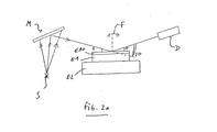
そのような周知の構成の一例が図2aに示されている。 An example of such a known configuration is shown in FIG. 2a.
この図は、そのX線束がモノクロメータMに向かって方向付けられたX線源Sを示している。 This figure shows an X-ray source S whose X-ray flux is directed towards the monochromator M.
サンプルE1はサンプル支持体E2によって支持されている。 Sample E1 is supported by sample support E2.
サンプルE1は、その表面上に、反射計によってその特徴が検査される薄膜E10を有している。 Sample E1 has on its surface a thin film E10 whose characteristics are inspected by a reflectometer.
モノクロメータ上での反射によって発せられた放射線は、サンプルに向かって方向付けられる。また、サンプル上での放射線の反射後、X線検出器Dが反射された放射線を受けてそれを解析することができる。 Radiation emitted by reflection on the monochromator is directed towards the sample. In addition, after reflection of the radiation on the sample, the X-ray detector D can receive the reflected radiation and analyze it.
矢印Fは、サンプル支持体およびそのサンプルの制御された移動を示している。 Arrow F shows the sample support and the controlled movement of the sample.
つまり、この周知の構成において、R(θ)の測定には、装置の機械的部材の移動を制御する必要がある。 That is, in this known configuration, it is necessary to control the movement of the mechanical member of the apparatus for measuring R (θ).
無論、これは、測定作業の持続時間に基づいて1つの結果を有する。例えばかなりの精度を要する移動も時間がかかる。 Of course, this has one result based on the duration of the measurement operation. For example, a movement that requires considerable accuracy takes time.
この第1のタイプの方法の第2の変形例においては、サンプルを不動状態に維持しかつサンプル上での放射線の反射後にその放射線を受ける検出器およびX線源の移動を制御することによりR(θ)測定を行なうことも知られている。この場合、X線源および検出器の移動は、サンプルに対して対称となるように制御される。 In a second variation of this first type of method, R is maintained by maintaining the sample stationary and controlling the movement of the detector and x-ray source receiving the radiation after reflection of the radiation on the sample. It is also known to perform (θ) measurement. In this case, the movement of the X-ray source and detector is controlled to be symmetric with respect to the sample.
そのような場合にも同様に、行なわれる移動が、測定値の取得時間にかなりの影響を与えることは言うまでもない。 In such a case as well, it goes without saying that the movements made have a considerable influence on the acquisition time of the measured values.
このように、R(θ)測定を行なうこれらの周知の方法は、比較的長い操作時間に関連付けられており、これこそが本質的な限界である(例えば、マイクロエレクトロニクス産業における薄膜解析等の用途において)。 Thus, these well-known methods of making R (θ) measurements are associated with relatively long operating times, which is an essential limitation (eg for applications such as thin film analysis in the microelectronics industry). In).
第2の周知のタイプのX線反射計方法において、サンプル上に達するビームの放射線の入射角分散は、1次元的または2次元的な光学的効果を引き起こすことができる光学アセンブリによって得られる。 In a second known type of X-ray reflectometer method, the incident angle dispersion of the radiation of the beam reaching the sample is obtained by an optical assembly that can cause a one-dimensional or two-dimensional optical effect.
この第2のタイプの方法は、角度分散X線反射計方法として知られている。 This second type of method is known as the angle dispersive X-ray reflectometer method.
そのような方法の原理が図3aに示されている。この図3aには、角度分散X線反射計測定を行なうことができる装置40の1次元的な図が示されている。
The principle of such a method is shown in FIG. In FIG. 3a, a one-dimensional view of an
この装置40は、
− X線を発生させて調整するための手段41(これらの手段は、X線源と、前記X線源から発せられるX線のビームを調整するための光学アセンブリとを備えており、光学アセンブリは所望の方法でサンプル42上へと方向付けられるX線ビームを調整することができる)と、
− X線検出器43と、
を備えている。
This
Means 41 for generating and adjusting X-rays (these means comprising an X-ray source and an optical assembly for adjusting the beam of X-rays emitted from said X-ray source; Can adjust the x-ray beam directed onto the sample 42 in any desired manner);
An X-ray detector 43;
It has.
手段41の光学アセンブリによって行なわれる調整は、サンプルに向かって方向付けられるX線ビームの制御された入射角分散に対応している。 The adjustment made by the optical assembly of means 41 corresponds to a controlled incidence angle dispersion of the X-ray beam directed towards the sample.
したがって、数度の角度分散をもってX線がサンプル上に到達することが求められる。 Therefore, it is required that X-rays reach the sample with an angular dispersion of several degrees.
本発明の好ましい用途においては、2度程度またはそれ以上の角度分散を得ることが求められる。 In a preferred application of the present invention, it is required to obtain an angular dispersion of about 2 degrees or more.
サンプルで反射されたビームは、その後、検出器43によって集められる。 The beam reflected by the sample is then collected by the detector 43.
手段41の光学アセンブリによって行なわれる光学的な調整が1次元的な効果(例えば、1つの寸法のみに沿う合焦)または2次元的な光学的効果に対応し得ることは言うまでもない。 It goes without saying that the optical adjustment performed by the optical assembly of the means 41 can correspond to a one-dimensional effect (for example focusing along only one dimension) or a two-dimensional optical effect.
一般に、検出器43は、PSD型(「位置敏感検出器」)であり、多数のピクセルを有するCCDまたはフォトダイオードタイプのセンサ430を備えている。
In general, the detector 43 is of the PSD type (“position sensitive detector”) and includes a CCD or
本発明の場合、また、一般に2次元光学素子の場合、検出器43は2次元検出器であっても良い。 In the case of the present invention, and generally in the case of a two-dimensional optical element, the detector 43 may be a two-dimensional detector.
2次元検出器は、入射角の同じ値に対応するピクセルを識別して再編することができる。 The two-dimensional detector can identify and reorganize pixels corresponding to the same value of incident angle.
また、この種の検出器は、異なる水平位置に配置されたピクセルが同じ入射角に対応し得るため(この場合、水平方向は図3aの平面に対して垂直な方向として規定される)、特に興味深い。 This type of detector also allows pixels located at different horizontal positions to correspond to the same angle of incidence (in this case, the horizontal direction is defined as the direction perpendicular to the plane of FIG. 3a), in particular. Interesting.
実際には、この第2の寸法(図の平面に対して垂直な寸法)に沿う特定の発散によって、サンプル上でのX線の入射角の弱い変化が引き起こされる。 In practice, a specific divergence along this second dimension (dimension perpendicular to the plane of the figure) causes a weak change in the angle of incidence of X-rays on the sample.
したがって、本発明が対象とする用途の場合、第2の寸法に沿う1度程度の発散は許容できる。 Accordingly, in the application targeted by the present invention, a divergence of about 1 degree along the second dimension is acceptable.
そのため、この種の2次元検出器は、2次元光学素子、特に本発明の光学アセンブリの場合のように重要な放射線束を2つの寸法に沿って集めることができる光学素子を有利に使用することができる。 Therefore, this type of two-dimensional detector advantageously uses two-dimensional optical elements, in particular optical elements that can collect important radiation bundles along two dimensions as in the case of the optical assembly of the present invention. Can do.
角度分散X線反射計測定においてビームの2次元調整を行なうため、第1の変形例においては、X線源から発せられるビームの光学アセンブリからの回折を利用することが知られている。この場合、光学アセンブリの表面は、2つの寸法に沿って湾曲された結晶である。 In order to perform a two-dimensional adjustment of the beam in an angular dispersive X-ray reflectometer measurement, it is known in the first variant to utilize diffraction from an optical assembly of a beam emitted from an X-ray source. In this case, the surface of the optical assembly is a crystal that is curved along two dimensions.
そのような結晶によれば、ブラッグの法則にしたがって行なわれるX線回折現象により、最初のビームを調整することができる。 According to such a crystal, the first beam can be adjusted by the X-ray diffraction phenomenon performed according to Bragg's law.
結晶におけるブラッグ条件がnλ=2dsinθBの形式を成していることを思い出されたい。ここで、nは反射の次数であり、λは回折が生じる入射放射線の波長であり、dは回折を伴う結晶の原子面同士の離間距離であり、θBは回折を発生させるために必要なこれらの同じ原子面上での入射角である。 Recall that the Bragg condition in the crystal is of the form nλ = 2 d sin θ B. Here, n is the order of reflection, λ is the wavelength of incident radiation at which diffraction occurs, d is the distance between the atomic planes of the crystal with diffraction, and θ B is necessary to generate diffraction. These are the incident angles on the same atomic plane.
X線入射ビームを考えると、結晶の特定の原子面群に対して良好に規定された入射角θBをもって結晶と衝突する波長がλの放射線は、先のブラッグ条件が満たされる場合、これらの同じ原子面上へ回折されなければならない。 Considering an X-ray incident beam, radiation with a wavelength of λ that collides with the crystal at a well-defined incident angle θ B for a particular group of atomic planes of the crystal, if the previous Bragg condition is satisfied, It must be diffracted onto the same atomic plane.
したがって、2つの寸法に沿って湾曲された結晶により、最初のビームに対して2次元的な効果を引き起こして、所望の調整を行なうことができる。 Thus, a crystal that is curved along two dimensions can cause a two-dimensional effect on the initial beam to achieve the desired adjustment.
つまり、この調整は、2つの異なる方向に沿う合焦に対応し得る。 That is, this adjustment can correspond to focusing along two different directions.
多層コーティングと比較した結晶の特徴は、そのような結晶に勾配を加えて結晶の有効領域を増大させることが難しいという点である。 A feature of crystals compared to multilayer coatings is that it is difficult to add a gradient to such crystals to increase the effective area of the crystals.
この点に関しては、Hildebrandtらによる文献「実際のX線光学素子へのアプローチ」(Rigakuジャーナル、第17刊、No.1/2000、特に18〜20頁)を参照することができる。 In this regard, reference can be made to the document “Approach to actual X-ray optical elements” by R. Hildebrandt et al. (Rigaku Journal, No. 17, No. 1/2000, especially pages 18-20).
これにより、結晶は、回折されるX線放射線束に関し、結晶上における入射放射線の入射角が大きく変化する結晶によって形成される光学アセンブリの方向に沿って制限される(勾配が存在しないため、集光面が限られる)。 This limits the crystal with respect to the diffracted X-ray radiation flux along the direction of the optical assembly formed by the crystal where the incident angle of incident radiation on the crystal varies greatly (since there is no gradient, The light surface is limited).
この方向は、結晶によって形成される光学アセンブリの経線方向に対応する。 This direction corresponds to the meridian direction of the optical assembly formed by the crystal.
2次元的な効果を引き起こす光学アセンブリによってビームの調整を行なうことから成る角度分散X線反射計の方法の第2の変形例においては、X線源からくる最初のビームの反射であって、米国特許第6,041,099号明細書に開示されているような「並行(side−by−side)」Kirkpatrick−Baez装置型の光学アセンブリ上での上記ビームの反射を使用することも知られている。 In a second variant of the method of angular dispersive X-ray reflectometry, comprising adjusting the beam by an optical assembly that causes a two-dimensional effect, the reflection of the first beam coming from the X-ray source, It is also known to use reflection of the beam on an optical assembly of the “side-by-side” Kirkpatrick-Baez apparatus type as disclosed in US Pat. No. 6,041,099. Yes.
KB装置の2つの各ミラーは、最初のビームX1をブラッグの法則にしたがって反射させることができる側方に勾配が付けられた多層コーティングを有していることが更に好ましい。 It is further preferred that each of the two mirrors of the KB device has a laterally graded multilayer coating that can reflect the initial beam X1 according to Bragg's law.
ここで、側方に勾配が付けられた多層体の定義に戻らなければならない。 Now we have to go back to the definition of a multi-layered body with lateral gradients.
これらの並行KB型の光学アセンブリによれば、最初のビームを調整することができる。 With these parallel KB type optical assemblies, the initial beam can be adjusted.
しかしながら、この本文で更に詳しく示されるように、そのような光学アセンブリを比較的重要な寸法に関連付けることができる。 However, as will be shown in greater detail in this text, such optical assemblies can be associated with relatively important dimensions.
無論、これにより、これらの周知の装置に制限が伴う。 Of course, this places limitations on these known devices.
したがって、角度分散X線反射計における用途においてR(θ)測定を行なうための周知の全ての解決策は、限界を伴う。 Thus, all known solutions for making R (θ) measurements in applications in angular dispersive x-ray reflectometers are limited.
これは、特に、150mmを超える合焦距離においてサンプル上での入射角における所望の分散が2度を超える場合であり、集められた放射線束が重要となるべき場合である(放射線の一般的な伝搬方向に対して垂直な方向に沿う約1度の角度分散)。 This is especially the case when the desired dispersion at the angle of incidence on the sample exceeds 2 degrees at a focal length of more than 150 mm, where the collected radiation bundle should be important (the generality of radiation An angular dispersion of about 1 degree along a direction perpendicular to the propagation direction).
本発明の他の目的は、これらの限界を解消できるようにすることである。 Another object of the invention is to be able to overcome these limitations.
前述した目的を達成するため、本発明は、第1の態様において、側方に勾配が付けられた反射多層体を有する光学アセンブリであって、上記反射多層体の反射面が、2次元的な光学的効果を引き起こしつつ、小さな入射角の入射X線を反射することができる光学アセンブリにおいて、上記反射面が1つの表面から成り、上記反射面は、2つの異なる方向に対応する2つの曲率にしたがって形成されていることを特徴とする光学アセンブリを提案する。 In order to achieve the above object, according to the first aspect of the present invention, there is provided an optical assembly having a reflective multilayer body having a lateral gradient, wherein the reflective surface of the reflective multilayer body is two-dimensional. In an optical assembly capable of reflecting incident X-rays with a small incident angle while causing an optical effect, the reflecting surface consists of one surface, and the reflecting surface has two curvatures corresponding to two different directions. Accordingly, an optical assembly characterized in that it is formed is proposed.
そのような光学的アセンブリの好ましい態様(しかしながら、これらに限定されない)は以下の通りである。 Preferred embodiments (but not limited to) of such optical assemblies are as follows.
− 上記側方勾配が入射X線の経線方向に沿って延びている、
− 上記反射面が滑らかである、
− 上記2次元的な光学的効果は、光学アセンブリ上での入射X線の単一の反射によって得られる、
− 上記異なる方向は、入射X線のサジタル方向および経線方向のそれぞれに対応している、
− 上記多層体が深さ勾配が付けられた多層体である、
− 上記反射面がCu−KαピークのX線を反射するようになっている、
− 上記反射面が略トロイダル状の幾何学的形状を成している、
− 上記反射面が略放物線状の幾何学的形状を成している、
− 上記反射面が略楕円状の幾何学的形状を成している、
− 上記反射面は、第1の方向に沿って略円形の幾何学的形状を成すとともに、第2の方向に沿って楕円または放物線状の幾何学的形状を成している、
− 上記反射面が20mm未満のサジタル曲率半径を有している、
− 光学アセンブリの入力および/または出力放射線束を制御するために、開口を有しかつX線を透過させない窓が光学アセンブリの入力および/または出力に関連付けられている、
− 上記窓が取り外し可能である、
− 上記窓の開口は、放射線の放射線束/発散間での妥協を実現するように寸法付けられている。
The lateral gradient extends along the meridian direction of the incident X-ray,
-The reflecting surface is smooth;
The two-dimensional optical effect is obtained by a single reflection of incident X-rays on the optical assembly;
The different directions correspond to the sagittal and meridian directions of the incident X-ray,
-The multilayer body is a multilayer body with a depth gradient;
The reflective surface is adapted to reflect Cu-Kα peak X-rays;
-The reflecting surface has a substantially toroidal geometric shape;
-The reflecting surface has a substantially parabolic geometric shape;
-The reflecting surface has a substantially elliptical geometric shape;
The reflective surface has a generally circular geometric shape along a first direction and an elliptical or parabolic geometric shape along a second direction;
The reflective surface has a sagittal radius of curvature of less than 20 mm;
A window having an aperture and not transmitting X-rays is associated with the input and / or output of the optical assembly to control the input and / or output radiation flux of the optical assembly;
-The window is removable;
The opening of the window is dimensioned to achieve a compromise between the flux / divergence of radiation.
また、第2の態様において、本発明は、前述した態様のうちの1つに係る光学アセンブリの製造方法であって、所定の曲率を既に有する基板のコーティングを含み、この基板の上記曲率が第2の異なる方向に沿っていることを特徴とする方法を提案する。 Also, in a second aspect, the present invention is a method of manufacturing an optical assembly according to one of the aforementioned aspects, comprising a coating of a substrate that already has a predetermined curvature, wherein the curvature of the substrate is We propose a method characterized by being along two different directions.
この製造方法の好ましい態様(しかしながら、これらに限定されない)は以下の通りである。 Preferred embodiments (but not limited to) of this production method are as follows.
− 基板が曲率を既に有している方向は、光学アセンブリのサジタル方向に対応している、
− 基板が湾曲される方向は、光学アセンブリの経線方向に対応している、
− 基板自体は、所定の曲率を既に有する管体、円錐体、または、擬似円錐体の形態を成す部材を原材料として構成され、上記曲率は、管体、円錐体、または、擬似円錐体の軸と垂直な方向に沿っている、
− 管体、円錐体、または、擬似円錐体の形態を成す上記部材は、10rmsよりも低い粗さを有するとともに、20mm未満のサジタル曲率半径を有している、
− 上記部材は、円形の横断面を有するガラス管である、
− 上記ガラスがデュラン型(登録商標)である、
− 基板の形成は、管体の長手方向に沿って管体をカットして、開かれた円筒体の形状を成す基板を得ることを含む、
− 管体の長手方向に沿ってカットした後、光学アセンブリの長さを寸法付けるようにカットする、
− 基板を湾曲する前に、多層体を構成するために上記コーティングが行なわれる、
− 多層体を構成するために基板をコーティングする前に、基板を湾曲させて基板を所望の幾何学的形状に合わせる、
− 入射X線を反射することが求められる所定の波長帯域の十分な伝送を確保しつつ望ましくないスペクトルバンドを減衰させるため、上記光学アセンブリがフィルタに接続される、
− 上記フィルタが10μmニッケルフィルタである、
− 上記フィルタは、
−− 光学アセンブリを収容する保護ハウジングの放射線入力窓および出力窓にそれぞれ位置されるとともに、その組み合わせた厚さが所望のフィルタ厚と一致する2つのフィルタを実現する技術、
−− 多層コーティング上に所定のコーティング厚をもってフィルタ材料から成る層を堆積させ、上記コーティング厚が、d=(e・sinθ)/2(ここで、eは必要とされるフィルタの「光学的な」厚さであり、θは光学素子上での入射角である)という関係によってほぼ与えられる技術、
のうちの一方によって実現される。
The direction in which the substrate already has a curvature corresponds to the sagittal direction of the optical assembly;
The direction in which the substrate is curved corresponds to the meridian direction of the optical assembly;
The substrate itself is composed of a material in the form of a tube, cone or pseudo-cone already having a predetermined curvature, the curvature being the axis of the tube, cone or pseudo-cone; Along the vertical direction,
The member in the form of a tube, cone or pseudo-cone has a roughness lower than 10 rms and a sagittal radius of curvature of less than 20 mm;
The member is a glass tube having a circular cross section;
The glass is a Duran type (registered trademark),
-Forming the substrate comprises cutting the tube along the length of the tube to obtain a substrate in the shape of an open cylinder;
-Cut along the length of the tube, then cut to dimension the length of the optical assembly;
-Before the substrate is bent, the coating is performed to form a multilayer body;
-Before coating the substrate to form a multilayer body, the substrate is bent to conform the substrate to the desired geometric shape;
The optical assembly is connected to a filter to attenuate undesired spectral bands while ensuring sufficient transmission of a predetermined wavelength band required to reflect incident X-rays;
The filter is a 10 μm nickel filter;
-The filter is
--- a technique for realizing two filters which are respectively located in the radiation input window and the output window of the protective housing containing the optical assembly and whose combined thickness matches the desired filter thickness;
-Deposit a layer of filter material on the multilayer coating with a predetermined coating thickness, where the coating thickness is d = (e · sin θ) / 2 (where e is the “optical” of the required filter ”Thickness, and θ is the angle of incidence on the optical element).
Realized by one of
また、第3の態様において、本発明は、X線を発生させて調整するための装置であって、X線源に接続された請求項1から15のいずれか一項に記載の光学アセンブリを有する角度分散X線反射計において適用できる装置において、上記X線源によって放射されたX線は、X線源によって放射されたビームをサンプルの目的に適合させるように2つの寸法に沿って調整され、X線は、対象のサンプル上に対して様々な入射角を有している装置を提案する。 Also, in a third aspect, the present invention provides an apparatus for generating and adjusting X-rays, the optical assembly according to any one of claims 1 to 15 connected to an X-ray source. In an apparatus applicable in an angular dispersive X-ray reflectometer, the X-rays emitted by the X-ray source are adjusted along two dimensions to adapt the beam emitted by the X-ray source to the purpose of the sample. , X-ray proposes a device with various incident angles on the sample of interest.
そのような装置の好ましい態様(しかしながら、これらに限定されない)は以下の通りである。 Preferred embodiments (but not limited to) of such devices are as follows.
− サンプル上における入射角の分散は、光学アセンブリによって反射されるビームのサジタル寸法に沿う角度分散と略一致している、
− 光学素子は、光学アセンブリの中心の法線がサンプルの表面と略平行になるようにサンプルに対して方向付けられる、
− サンプルの高さにおける取得角度は、光学アセンブリのサジタル寸法に対応する第1の寸法に沿って2度よりも大きく、光学アセンブリの経線寸法に対応する第2の寸法に沿って約1度であり、光学アセンブリは、サンプル上におけるX線の入射角の分散が2度よりも大きくなるように位置決めされ、サンプルは、光学アセンブリに対して15cmを超える距離をもって位置されている。
The dispersion of the incident angle on the sample is approximately coincident with the angular dispersion along the sagittal dimension of the beam reflected by the optical assembly;
The optical element is oriented relative to the sample such that the normal of the center of the optical assembly is substantially parallel to the surface of the sample;
The acquisition angle at the height of the sample is greater than 2 degrees along the first dimension corresponding to the sagittal dimension of the optical assembly and about 1 degree along the second dimension corresponding to the meridian dimension of the optical assembly; And the optical assembly is positioned such that the dispersion of the incident angle of X-rays on the sample is greater than 2 degrees, and the sample is positioned at a distance greater than 15 cm relative to the optical assembly.
本発明の他の態様、目的、利点は、前述した図1a,2a,3aに加えて本発明の好適な実施形態の以下の開示内容および添付図面を参照することにより明らかとなる。 Other aspects, objects and advantages of the present invention will become apparent by reference to the following disclosure of the preferred embodiment of the present invention and the accompanying drawings in addition to the above-described FIGS. 1a, 2a and 3a.
この開示の序文においては、図が本発明の原理を示そうとするものであり寸法および縮尺を実際の態様で必ずしも示していないことが明記されている。 In the introductory part of this disclosure, it is specified that the figures are intended to illustrate the principles of the invention and do not necessarily show the dimensions and scale in an actual manner.
このことは、X線の入射角(または反射角)において特に当てはまる。 This is particularly true at the incident angle (or reflection angle) of X-rays.
これらのX線は、実際には、10度未満の入射角をもって本発明に係る反射面上に達する。 These X-rays actually reach the reflecting surface according to the present invention with an incident angle of less than 10 degrees.
また、経線方向およびサジタル方向も、X線ビームの一般的な伝搬方向に対して規定される。 The meridian direction and the sagittal direction are also defined with respect to the general propagation direction of the X-ray beam.
− 経線方向は、このビームの平均伝搬方向に対応している(より正確には、対象の光学アセンブリ上でのビームの反射前のビームの平均伝搬方向と反射後のビームの平均伝搬方向との間の平均的な方向に対応している)、
− サジタル方向は、この経線方向に対して垂直な水平方向に対応している(ここで、垂直とは、X線の入射ビームを反射させるために使用される対象の光学アセンブリの反射面の部分に対する平均的な法線として規定される)。
The meridian direction corresponds to the average propagation direction of this beam (more precisely, the average propagation direction of the beam before and after reflection of the beam on the optical assembly of interest; Corresponding to the average direction between)
The sagittal direction corresponds to the horizontal direction perpendicular to this meridian direction (where vertical is the part of the reflective surface of the optical assembly of interest used to reflect the incident beam of X-rays) Defined as the average normal to).
本発明で考慮される光学アセンブリの開示
ここで、図1を参照すると、X線源Sからくる入射X線を反射するように形成された光学アセンブリ10が示されている。
Disclosure of Optical Assembly Considered by the Present Invention Referring now to FIG. 1, an optical assembly 10 is shown that is configured to reflect incident X-rays coming from an X-ray source S.
X線源Sは、特に、X線チューブや回転陽極から成っていても良く、あるいは、マイクロフォーカスX線源タイプのものであっても良い。 The X-ray source S may in particular consist of an X-ray tube or a rotating anode, or may be of the microfocus X-ray source type.
光学アセンブリ10は、基板(例えばガラス)上に形成されかつ入射X線のための反射面を形成する多層構造を有している。 The optical assembly 10 has a multilayer structure formed on a substrate (eg, glass) and forming a reflective surface for incident x-rays.
この光学アセンブリの反射面は、特有の幾何学的形状を成している。 The reflective surface of this optical assembly has a unique geometric shape.
より正確には、この反射面は、2つの異なる方向に対応する2つの曲率にしたがって形成されている。 More precisely, the reflecting surface is formed according to two curvatures corresponding to two different directions.
そのため、この反射面は、米国特許第6,041,099号明細書が対象とするような光学アセンブリで使用されるタイプの反射面と大きく異なっている。すなわち、
− 2つの異なる基本的なミラーが組み付けられた光学アセンブリにおける場合とは異なり、この反射面は1つの反射面であり、
− この反射面は滑らか(この表現は、本文においては、反射面が第2級の不連続性(頂部、角部−凸部または窪み−等)を全く有していないことを意味している)であり、
− また、大きな違いは、本発明の場合には、入射線だけが単一の反射を受けることにより、所望の2次元的な光学的効果を生じるのに対し、米国特許第6,041,099号明細書に開示された光学アセンブリの場合には、2つの反射が必要であるという点である。
As such, this reflective surface is very different from the type of reflective surface used in optical assemblies such as that described in US Pat. No. 6,041,099. That is,
-Unlike in an optical assembly with two different basic mirrors assembled, this reflective surface is a single reflective surface;
-This reflective surface is smooth (this expression means in the text that the reflective surface does not have any secondary discontinuities (tops, corners-projections or depressions, etc.). ) And
-Also, the major difference is that in the case of the present invention, only the incident line receives a single reflection resulting in the desired two-dimensional optical effect, whereas US Pat. No. 6,041,099. In the case of the optical assembly disclosed in the specification, two reflections are necessary.
更に正確には、本発明に係る光学アセンブリの反射面は、経線方向Xで曲率Rxを有するとともに、サジタル方向Yで曲率Ryを有している。 More precisely, the reflecting surface of the optical assembly according to the present invention has a curvature Rx in the meridian direction X and a curvature Ry in the sagittal direction Y.
図1はこれらの曲率半径を示している。各曲率半径Rx,Ryによって規定される曲線の外形を表わすために、2つの曲線Cx,Cyが示されている。 FIG. 1 shows these radii of curvature. Two curves Cx, Cy are shown to represent the contour of the curve defined by the respective radii of curvature Rx, Ry.
2つの曲率半径のそれぞれは、一定であっても良く、あるいは、その対応する曲線に沿って変化しても良い。 Each of the two radii of curvature may be constant or may vary along its corresponding curve.
すなわち、各曲線Cx,Cyは、円であっても良いが、楕円、放物線、あるいは、他の曲線(開いた曲線または閉じた曲線)であっても構わない。 That is, each of the curves Cx and Cy may be a circle, but may be an ellipse, a parabola, or another curve (open curve or closed curve).
いずれにせよ、光学アセンブリ10の反射面は、単純な球面形状を有していない(すなわち、半径Rx,Ryは等しくなく一定でもない)。 In any case, the reflective surface of the optical assembly 10 does not have a simple spherical shape (ie, the radii Rx, Ry are not equal or constant).
したがって、各曲線Cx,Cyは、空間内の異なる方向(ここで対象にしている例では、2つの直交する方向)に関連付けられている。 Accordingly, each curve Cx, Cy is associated with a different direction in space (in the example here, two orthogonal directions).
これらの曲線のそれぞれは、反射面で反射されるX線に対して1次元的な光学的効果を引き起こす。すなわち、
− 曲線Cxは、方向Xに沿って1次元的な光学的効果を引き起こし、
− 曲線Cyは、Y方向に沿って1次元的な光学的効果を引き起こす。
Each of these curves causes a one-dimensional optical effect on the X-rays reflected by the reflecting surface. That is,
The curve Cx causes a one-dimensional optical effect along the direction X;
The curve Cy causes a one-dimensional optical effect along the Y direction.
また、これらの各次元効果は、曲線に関連付けられた曲率によって決まるとともに、この曲線に沿う上記曲率の展開(曲率変化の態様)によって決まる。 Each of these dimensional effects is determined by the curvature associated with the curve, and is also determined by the development of the curvature along the curve (mode of curvature change).
したがって、曲線Cx,Cyは、対応する1次元的な光学的効果、例えば1次元的な視準(平行化)または1次元的な合焦を選択的に得るように設定されたパラメータを有していても良い。 Thus, the curves Cx, Cy have parameters set to selectively obtain corresponding one-dimensional optical effects, for example one-dimensional collimation (parallelization) or one-dimensional focusing. May be.
図1は、各曲線Cx,Cyが1次元的な合焦を引き起こしている場合を示している。 FIG. 1 shows a case where the curves Cx and Cy cause one-dimensional focusing.
この目的を達成するため、Rx,Ryは、互いに異なっているが、一定のままである(曲線Cx,Cyは円である)。 To achieve this goal, Rx and Ry are different from each other but remain constant (curves Cx and Cy are circles).
したがって、この好適な実施形態において、光学アセンブリの反射面はトロイダル形状を成している。 Thus, in this preferred embodiment, the reflective surface of the optical assembly has a toroidal shape.
これは、X線源Sからくる発散したX線を1つの像点Iに集束させる2次元合焦を引き起こしている。 This causes two-dimensional focusing in which divergent X-rays coming from the X-ray source S are focused on one image point I.
また、本発明の好ましい用途によれば、曲率半径Ry(サジタル方向の曲率半径)は、短い距離すなわち90cm未満の距離にわたる合焦のために必要な20mm未満の値を有している(この実施形態では、他の場合と同様)。以下、この態様について説明する。 Also, according to a preferred application of the present invention, the radius of curvature Ry (the radius of curvature in the sagittal direction) has a value less than 20 mm required for focusing over a short distance, i.e. less than 90 cm (this implementation). The form is the same as other cases). Hereinafter, this aspect will be described.
なお、本発明に係る光学アセンブリによれば、多層コーティング「モンテル」型のミラーに関してこの本文の序文で説明した欠点を解消することができる。 It should be noted that the optical assembly according to the present invention can eliminate the disadvantages described in the introduction of this text regarding the multilayer coating “Montell” type mirror.
特に、前述したように、この光学アセンブリは単一部品である(精巧な組立が不要である)。 In particular, as mentioned above, this optical assembly is a single piece (no elaborate assembly is required).
また、入射X線だけがその反射面上で単一の反射を受ける。 Also, only incident X-rays undergo a single reflection on the reflecting surface.
更に、反射面は1つでありかつ滑らかである。 Furthermore, there is one reflecting surface and it is smooth.
以上、光学アセンブリ10の反射面が多層体によって形成されている点について述べてきた。 As described above, the point that the reflection surface of the optical assembly 10 is formed of a multilayer body has been described.
この多層体は(この本文で対象とする全ての多層体と同様に)、最低でも1つの「側方勾配」を有している。 This multilayer (as with all multilayers covered in this text) has at least one “lateral slope”.
この特徴により、反射面に対して異なる局部入射角を有するX線を効果的に反射させることができる。 With this feature, X-rays having different local incident angles with respect to the reflecting surface can be effectively reflected.
実際には、反射面の異なる領域が入射X線を同じ局部入射角で受けることは言うまでもない(入射ビームの発散およびこの反射面の幾何学的形状に起因する)。 In practice, it goes without saying that different regions of the reflecting surface receive incident X-rays at the same local angle of incidence (due to the divergence of the incident beam and the geometry of this reflecting surface).
側方に勾配が付けられた多層体とは、ここでは、ミラーの有効領域の全ての点でブラッグの条件が尊重されるようにその層構造が適合されている多層体のことを意味している。 A laterally graded multilayer means here a multilayer whose structure is adapted so that the Bragg conditions are respected at all points in the effective area of the mirror. Yes.
ここで、ブラッグの条件がnλ=2d×sinθの式から成ることを思い出されたい。この場合、
n:反射の次数
λ:入射放射線の波長
d:多層体の周期
θ:多層体の表面上における入射角
である。
Recall that the Bragg condition consists of the equation nλ = 2d × sin θ. in this case,
n: Order of reflection λ: Wavelength of incident radiation d: Period of multilayer body θ: Angle of incidence on the surface of the multilayer body.
したがって、例えば銅kαラインを含む狭い波長帯域(波長のCu−kαピークが約0.154nm)に沿って入射X線を放射する場合、側方に勾配が付けられた多層ミラーは、ミラーの有効領域全体にわたってブラッグの条件を維持することができる。 Thus, for example, when emitting incident X-rays along a narrow wavelength band including the copper kα line (wavelength Cu-kα peak is about 0.154 nm), a laterally graded multilayer mirror is effective for the mirror. Bragg conditions can be maintained throughout the region.
これにより、入射線の局部入射角が変動するミラーの異なる領域で所定の波長帯域が反射される(銅kαピークを含む前述した例において)。 As a result, the predetermined wavelength band is reflected in different regions of the mirror where the local incident angle of the incident line varies (in the example described above including the copper kα peak).
したがって、有効に使用されるミラーの表面を増大させることができる。 Therefore, the surface of the mirror used effectively can be increased.
勾配は、適合された態様で多層体の周期を局部的に変えることにより得られる。 The gradient is obtained by locally changing the period of the multilayer body in an adapted manner.
すなわち、側方に勾配が付けられたこの種の多層構造により、光学アセンブリの立体集束角度(solid collection angle)を大きくすることができ、それにより、光学的な幾何学形状が同じ場合には、全反射によって作用する単層ミラーに対して高い反射放射線束が得られる。 That is, this type of multi-layered structure with lateral gradients can increase the solid collection angle of the optical assembly, so that if the optical geometry is the same, A high reflected radiation bundle is obtained for a single-layer mirror acting by total reflection.
また、側方勾配の存在により、特定の周知の構成、例えばX線源と光学素子との間の距離および光学素子とサンプルとの間の距離が等しくかつ小型の光学素子においては光学素子上における入射角の変化を僅かに留めることができるローランド円を使用する構成の限界に打ち勝つことができる。 Also, due to the presence of lateral gradients, certain well-known configurations such as the distance between the X-ray source and the optical element and the distance between the optical element and the sample are equal and small on the optical element. The limitations of the configuration using the Roland circle, which can keep the change in incident angle slightly, can be overcome.
実際には、ローランド円を使用する構成は、勾配が無い光学素子の使用を可能にするが、X線源に対する結像領域の拡大または縮小を行なうことができないという限界を有している(X線源と比較した結像領域の縮小は、スリットの使用によるものと考えることができるが、この方法は、あまり正確ではなく、集められた放射線束を制限する)。 In practice, the configuration using the Roland circle allows the use of optical elements without gradients, but has the limitation that the imaging region cannot be enlarged or reduced with respect to the X-ray source (X Although the reduction of the imaging area compared to the source can be attributed to the use of slits, this method is less accurate and limits the collected radiation flux).
この種の周知の構成の一例は、Sasanumaらによる文献「W/Si多層体の二重に湾曲したモノクロメータを使用する点収束小角X線散乱カメラ」(科学機器の評論、アメリカ物理学会、ニューヨーク、第67刊、No.3、1996年3月1日(688頁〜692頁))において見出すことができる。 An example of this type of well-known configuration is the document by Sasanuma et al., "Point-focusing small-angle X-ray scattering camera using a W / Si multilayer doubly curved monochromator" (Science Instrument Review, American Physical Society, New York 67, No. 3, March 1, 1996 (pp. 688 to 692)).
また、本発明の様々な実施形態の多層体が深さ勾配(多層体の厚さにおける勾配)を有していても良いことは言うまでもない。 It goes without saying that the multilayer body of various embodiments of the present invention may have a depth gradient (gradient in the thickness of the multilayer body).
そのような深さ勾配により、入射角が固定されかつ波長が変動する場合において、あるいは、その逆において、ブラッグ条件を満たすことができる。 Such a depth gradient can satisfy the Bragg condition when the incident angle is fixed and the wavelength varies, or vice versa.
したがって、例えば、光学アセンブリの多層体の波長における通過帯域の幅を大きくすることができるとともに、同じ所定の像平面の高さで様々な波長のX線を合焦しあるいは視準することができる(幾何学的構成が固定されている場合、すなわち、光学アセンブリおよび像平面の入射線の源に対する相対位置が固定されている構成)。 Thus, for example, it is possible to increase the width of the passband at the wavelength of the multilayer body of the optical assembly and to focus or collimate X-rays of various wavelengths at the same predetermined image plane height. (If the geometric configuration is fixed, i.e. the configuration relative to the optical assembly and the source of the incident line of the image plane is fixed).
このようにすると、波長が異なる複数のX線源を使用して、X線源および/または像平面を光学アセンブリに対して再び位置決めする必要なく、同じ光学アセンブリを用いて異なるX線源からくるX線を反射することができる。 In this way, multiple X-ray sources with different wavelengths can be used to come from different X-ray sources using the same optical assembly without having to reposition the X-ray source and / or image plane relative to the optical assembly. X-rays can be reflected.
この場合には、光学アセンブリの波長許容範囲(許容範囲Δλ)が使用される。 In this case, the wavelength tolerance (allowance Δλ) of the optical assembly is used.
同様に、この許容範囲Δλを許容範囲Δθに変換することもできる。 Similarly, the allowable range Δλ can be converted into the allowable range Δθ.
実際に、ブラッグ条件の枠内では、波長の許容範囲が入射角の許容範囲と一致しており、入射ビームの波長が一定の場合、同じ波長を有するその光線同士が異なる局部入射角を有する入射光束を集光して反射することができる。 Actually, within the Bragg condition frame, the allowable range of the wavelength coincides with the allowable range of the incident angle, and when the incident beam has a constant wavelength, the incident light beams having the same wavelength have different local incident angles. The light beam can be collected and reflected.
このようにすれば、特に、寸法が大きいX線源を使用することができる(角度許容範囲の増大)。 In this way, in particular, an X-ray source with a large dimension can be used (increase in angle tolerance).
ここで図2を参照すると、本発明の他の好適な実施形態が光学アセンブリ20として示されている。 Referring now to FIG. 2, another preferred embodiment of the present invention is shown as optical assembly 20.
この光学アセンブリの多層体の反射面は、それぞれが放物線および円である2つの曲線Cx,Cyに沿って各方向X,Yに形成されている。これらの各曲線は、その対応するX方向またはY方向に沿って視準を行なっている。 The reflecting surface of the multilayer body of this optical assembly is formed in each direction X, Y along two curves Cx, Cy, each of which is a parabola and a circle. Each of these curves collimates along the corresponding X or Y direction.
したがって、空間内の全ての方向に沿う平行視準ビームが発散入射ビームから形成される。 Thus, a collimated collimated beam along all directions in space is formed from the diverging incident beam.
すなわち、本発明によれば、多層ミラー(側方に勾配が付けられ、可能であれば更に深さ勾配を有する)から成る光学アセンブリであって、その反射面が任意の様々な複雑な非球面形状のうちのある1つの形状を成すことができる光学アセンブリを実現することができる。 That is, according to the present invention, an optical assembly consisting of a multi-layer mirror (graded on the side, possibly with a depth gradient if possible), the reflective surface of which can be any various complex aspherical surface. An optical assembly capable of forming one of the shapes can be realized.
したがって、特に、この反射面に対しては、以下の幾何学的形状のうちの1つを与えることができる。 Thus, in particular, this reflective surface can be given one of the following geometric shapes:
− 略トロイダル状の幾何学的形状
− 略放物線状の幾何学的形状
− 略楕円状の幾何学的形状
− 第1の方向(特にサジタル方向)に沿って略円形状を成しかつ第2の方向(特に経線方向)に沿って楕円または放物線状を成す幾何学的形状。
-A substantially toroidal geometric shape-a substantially parabolic geometric shape-a substantially elliptical geometric shape-a substantially circular shape along a first direction (especially the sagittal direction) and a second A geometric shape that is elliptical or parabolic along a direction (especially the meridian direction).
側方勾配は、特に、入射X線の経線方向に沿って延びていても良い。 In particular, the lateral gradient may extend along the meridian direction of the incident X-ray.
Cu−Kαピークの放射線を反射させるために、多層体の周期が合わせられても良い。 In order to reflect the radiation of the Cu—Kα peak, the period of the multilayer body may be adjusted.
ここで図3を参照すると、2つの端壁31,32が設けられた本発明に係る光学アセンブリ30が示されている。これらの端壁31,32はそれぞれ、この光学アセンブリによって反射されるべき放射線の入力断面および出力断面にそれぞれ位置されている。
Referring now to FIG. 3, there is shown an optical assembly 30 according to the present invention in which two
各端壁31,32は、X線放射が通過できる開口(それぞれ310,320)を有している。この場合、端壁自体はX線を透過させない。
Each
端壁は、例えば鉛によって形成されていても良い。 The end wall may be made of lead, for example.
また、(入力断面に位置する開口による)入射放射線束と(出力断面に位置する開口による)反射した放射線を制御するために、(他の開口とは無関係に)各開口の形状およびサイズを調整することができる。 Also, adjust the shape and size of each aperture (regardless of other apertures) to control the incident radiation bundle (due to the apertures located in the input cross section) and the reflected radiation (due to the apertures located in the output cross section) can do.
したがって、これらの開口は、(入力または出力の際に)放射線束の強度とその発散との間で妥協を見出すように寸法付けることができる。 These apertures can thus be dimensioned to find a compromise between the intensity of the radiation bundle and its divergence (on input or output).
端壁31,32を取り外し可能に形成できること、例えば図3に示されるように端壁31,32を光学アセンブリの水平な横方向端部に対して螺合するように形成できることは言うまでもない。
Needless to say, the
このようにすれば、必要に応じて所望の放射線束/発散間で妥協を見出すために、光学アセンブリを柔軟な態様で適合させることができる。 In this way, the optical assembly can be adapted in a flexible manner to find a compromise between the desired flux / divergence as needed.
また、入力壁または出力壁を単独で考慮することもできる。 Also, the input wall or the output wall can be considered alone.
したがって、その開口に対応する各端壁は、X線が通過できる「窓」を構成する。 Therefore, each end wall corresponding to the opening constitutes a “window” through which X-rays can pass.
好ましい製造方法の開示
ここで、先に開示されたタイプの光学アセンブリを得ることができる一方で以下の利点が得られる好ましい方法について説明する。
Disclosure of Preferred Manufacturing Method Now, a preferred method will be described in which an optical assembly of the type disclosed above can be obtained while the following advantages are obtained.
− 多層コーティングを行なうために使用される基板の表面状態を非常に良好に確保することができる(X線多層ミラーの基板における表面粗さ仕様は、通常、約10オングストロームrms(2乗平均平方根)の最大値を超えてはならない粗さ程度となっている)。 -The surface condition of the substrate used to perform the multi-layer coating can be ensured very well (the surface roughness specification on the substrate of the X-ray multi-layer mirror is usually about 10 angstrom rms (root mean square)) The roughness should not exceed the maximum value).
− また、一方で、例えば20mm未満の値を有する極端に減少したサジタル方向の曲率半径Ry(例えば90cm未満の線源−合焦点距離に沿って合焦を行なうことができる)に沿って表面を構成することもできる。 Also, on the other hand, the surface along an extremely reduced sagittal radius of curvature Ry having a value of eg less than 20 mm (eg a source of less than 90 cm—focusing can be performed along the focal length). It can also be configured.
実際には、以下の方法によってそのような曲率半径の値および表面状態を有する多層体をコーティングするための基板表面を得ることは難しい。 In practice, it is difficult to obtain a substrate surface for coating a multilayer body having such a value of curvature radius and surface state by the following method.
− そのような低いサジタル曲率を既に有している基板を研磨する。この場合、予め成形された基板の研磨は微細である。 Polishing a substrate that already has such a low sagittal curvature. In this case, the pre-shaped substrate is finely polished.
− あるいは、既に研磨された平坦な基板をサジタル曲率半径Ryに沿って曲げる。この場合、所望の低い曲率半径を得ることは難しい(一方、そのような曲率半径により、所望の光学的効果を短い距離にわたって引き起こすことができ、それにより、光学アセンブリの占有空間を減少させることができる)。 Alternatively, a flat substrate that has already been polished is bent along the sagittal radius of curvature Ry. In this case, it is difficult to obtain the desired low radius of curvature (while such radius of curvature can cause the desired optical effect over a short distance, thereby reducing the footprint of the optical assembly. it can).
本発明に係る製造方法の場合には、特別の処理を全く行なうことなく、曲率方向に沿って既に1つの曲率を有する基板を使用して光学アセンブリを形成することにより、所望の表面状態が得られる。 In the case of the manufacturing method according to the present invention, a desired surface state is obtained by forming an optical assembly using a substrate that already has one curvature along the direction of curvature without any special treatment. It is done.
光学アセンブリが製造されてX線源に対して位置決めされた際には、基板が既に曲率を有している方向が、光学アセンブリのサジタル方向と一致していることが更に好ましい(この方向は、前述したように、入射放射線に対して規定されているが、入射放射線に対して光学アセンブリが特定の方法で方向付けられる範囲で光学アセンブリ自体に対してもできる限り規定される)。 More preferably, when the optical assembly is manufactured and positioned relative to the x-ray source, the direction in which the substrate already has a curvature coincides with the sagittal direction of the optical assembly (this direction is As stated above, it is defined for incident radiation, but as much as possible for the optical assembly itself to the extent that the optical assembly is directed in a particular manner relative to incident radiation).
そのような基板は、反射面を支持する光学アセンブリの面に対応する面を有している。基板のこの面は、「光学面」と呼ばれる。 Such a substrate has a surface corresponding to the surface of the optical assembly that supports the reflective surface. This surface of the substrate is called the “optical surface”.
したがって、一般に、本発明においては、(更に好ましくは、光学アセンブリのサジタル方向と一致するように設定された方向に沿って)曲率を既に有している基板が使用され、また、この基板は、異なる第2の方向(更に好ましくは、光学アセンブリの経線方法に対応する方向)に沿って湾曲される。 Thus, in general, in the present invention, a substrate that already has a curvature (and more preferably along a direction set to coincide with the sagittal direction of the optical assembly) is used, and the substrate is Curved along a different second direction (more preferably a direction corresponding to the meridian method of the optical assembly).
多層体を有する基板の光学面のコーティングも行なわれる。このコーティングは、基板の湾曲前あるいは湾曲後に行なうことができる。 Coating of the optical surface of a substrate having a multilayer body is also performed. This coating can be performed before or after the substrate is curved.
いずれにせよ、光学アセンブリはこのようにして得られる。 In any case, the optical assembly is obtained in this way.
所望の曲率(形状において、また、曲率半径の値において)を有する基板を選択することにより、また、その基板を望み通りに湾曲することにより、所望の幾何学的形状を有する光学アセンブリを得ることができる。 By selecting a substrate having the desired curvature (in shape and in the value of the radius of curvature) and bending the substrate as desired, an optical assembly having the desired geometric shape is obtained. Can do.
また、管体、円錐体、あるいは、擬似円錐体(ここでは、その回転軸に対して傾きかつ空間内で回転軸をカットすることにより生じる直線を楕円等の曲線に沿って回転することによって形成される回転面として規定される)等の部材(特にガラスによって形成された部材)を特に使用することにより基板自体を構成することもできる。 In addition, a tube, a cone, or a pseudo-cone (here, formed by rotating a straight line generated by cutting the rotation axis in the space and along an ellipse or the like with respect to its rotation axis) The substrate itself can also be configured by using in particular a member (particularly a member made of glass) such as a rotating surface that is defined.
管体の形態を成す部材の場合、管体は、円形の横断面を有することができるが、楕円であっても良く、あるいは、任意の閉じられた曲線の横断面を有していても良い。 In the case of a member in the form of a tubular body, the tubular body may have a circular cross section, but it may be oval or have any closed curved cross section. .
また、そのような部材は、その準線が放物線の一部等の開かれた曲線である開かれた円筒体であっても良い。 Moreover, such a member may be an open cylinder whose quasi-line is an open curve such as a part of a parabola.
いずれにせよ、原材料となる部材は、更に好ましくは、製造が求められる光学アセンブリのサジタル方向に対応する方向に沿って1つの曲率を有している。 In any case, the member that is the raw material preferably has one curvature along a direction corresponding to the sagittal direction of the optical assembly that is desired to be manufactured.
この方向は、管体の軸、円錐体の軸、あるいは、擬似円錐体の軸と直交している。 This direction is orthogonal to the axis of the tube, the axis of the cone, or the axis of the pseudo cone.
好適な実施形態において、そのような基板は、特に、その横断面が円形を成すガラス管を使用して得ることができる。 In a preferred embodiment, such a substrate can be obtained in particular using a glass tube whose cross section is circular.
この好適な実施形態において、光学アセンブリの製造に必要でかつ1つの方向に沿って1つの曲率を有する基板は、特に、以下の方法によって得ることができる。 In this preferred embodiment, the substrate necessary for the manufacture of the optical assembly and having one curvature along one direction can be obtained in particular by the following method.
− 所望のサジタル曲率半径を有するガラス管、例えばSCHOTT社によって製造されるデュラン型(登録商標)のガラス管をカットし、
− このようにしてカットされた管をコーティング材料で連続的にコーティングして、管上に多層体を構成する。
-Cutting glass tubes with the desired sagittal radius of curvature, for example Duran® glass tubes manufactured by SCHOTT,
-The tube cut in this way is continuously coated with a coating material to form a multilayer body on the tube.
そのような基板は、その後、1つの方向(好ましくは経線方向)に沿って所望の曲率で湾曲され、これにより、光学アセンブリが得られる。 Such a substrate is then curved with a desired curvature along one direction (preferably the meridian direction), thereby obtaining an optical assembly.
また、他の場合と同様にこの実施形態においても、最初に部材(ここでは、カットされた管体)を湾曲し、その後にコーティングを行なうことができることは言うまでもない。 Further, as in the other cases, in this embodiment, it goes without saying that the member (here, the cut tube) can be bent first and then the coating can be performed.
本発明に係る方法を実施する全ての実施形態においては、このように形成された多層体が側方に勾配が付けられた多層体(できる限り、垂直勾配も有している)であることは言うまでもない。 In all embodiments of carrying out the method according to the invention, the multilayer body thus formed is a laterally sloped multilayer body (with vertical gradient as much as possible) Needless to say.
ガラス管の対称軸(半管を形成するためにこの対称軸を含んでいても良い)と平行な方向に沿って切断を行なうことにより、ガラス管の長手方向に沿ってガラス管のカットが行なわれ、これにより、開かれた円筒体の形態を成す基板が得られる。 The glass tube is cut along the longitudinal direction of the glass tube by cutting along a direction parallel to the axis of symmetry of the glass tube (which may be included to form a semi-tube) This gives a substrate in the form of an open cylinder.
したがって、この好適な実施形態において、この開かれた円筒体の準線は、円の一部、例えば半円の形状を成している。 Thus, in this preferred embodiment, the open cylindrical quasi-line is in the form of a part of a circle, for example a semicircle.
この長手方向のカット後にもう1つのカットが行なわれることにより、光学素子の長さ寸法が決定される。 By performing another cut after this longitudinal cut, the length dimension of the optical element is determined.
これらのカッティング作業後、このようにして構成された基板は、本発明に係る光学アセンブリの製造のために使用される。 After these cutting operations, the substrate thus configured is used for the production of the optical assembly according to the invention.
基板を多層体でコーティングした後、コーティングされた基板は、経線方向に対応する所望の第2の方向に沿って湾曲され、これにより、所望の幾何学的形状にしたがって多層体の表面を適合させる。 After coating the substrate with the multilayer body, the coated substrate is curved along a desired second direction corresponding to the meridian direction, thereby adapting the surface of the multilayer body according to the desired geometric shape. .
このように、本発明に係る光学アセンブリの製造方法のこの好適な実施形態においては、円形の一部の形状をほぼ成す準線を有する円筒状基板を形成することができ、その後、そのような基板のコーティングが行なわれ、上記基板の円筒の準線の面内に含まれない方向に沿って(特に、円筒体の母線の方向に沿って)基板が湾曲される。 Thus, in this preferred embodiment of the method of manufacturing an optical assembly according to the present invention, it is possible to form a cylindrical substrate having a quasi-line that is substantially part of a circular shape, and thereafter The substrate is coated and the substrate is curved along a direction that is not included in the plane of the cylindrical quasi-line of the substrate (especially along the direction of the generatrix of the cylinder).
したがって、本発明に係る光学アセンブリを製造することは、前述した技術(所望の幾何学的形状に既に完全に合わせられている基板に対してコーティングを施す技術、あるいは、平面的な多層体の2つの方向に沿って湾曲する技術)のうちの1つを使用するよりもかなり簡単であることに出願人は気付いた。 Therefore, the production of an optical assembly according to the present invention can be achieved by using the techniques described above (the technique of applying a coating to a substrate that is already perfectly matched to the desired geometric shape, or two-dimensional multilayer body). Applicants have found that it is much simpler than using one of the techniques of bending along one direction.
つまり、その後に多層体をコーティングするために使用される基板であって、非常に良好な表面状態(粗さが10オングストロームrmsを超えない)と低いサジタル曲率半径(20mm未満)とを有する基板を得ることができる。 That is, a substrate that is subsequently used to coat a multilayer body with a very good surface condition (roughness not exceeding 10 angstrom rms) and a low sagittal radius of curvature (less than 20 mm). Can be obtained.
そのため、短い距離にわたって光学的効果を得ることができる。 Therefore, an optical effect can be obtained over a short distance.
2つの1次元的な合焦の場合、トロイダルミラーに関しては、以下の式によって接線(経線)合焦の特徴とサジタル合焦の特徴とが与えられることを思い出されたい。 Recall that in the case of two one-dimensional focusing, for the toroidal mirror, the following formula gives the tangential (meridian) and sagittal focusing characteristics:
− 接線合焦:1/p+1/q=2/(Rxsinθ)
ここで、pはX線源とミラーとの間の距離、qはミラーと合焦面との間の距離、θは入射角である。
-Tangential focusing: 1 / p + 1 / q = 2 / (Rxsinθ)
Here, p is the distance between the X-ray source and the mirror, q is the distance between the mirror and the focal plane, and θ is the incident angle.
− サジタル合焦:1/p+1/q=2sinθ/Ry
(2つの寸法に沿う合焦の場合、pおよびqの距離は2つの式に関して同一である)
変形例として、その準線が開かれている円筒体を形成しかつコーティングと第2の方向での湾曲との順番を先に開示した順番と逆にするために、カットされた管体の同じ部分で始めることもできることは言うまでもない。
-Sagittal focus: 1 / p + 1 / q = 2 sin θ / Ry
(For focusing along two dimensions, the distance between p and q is the same for the two equations)
As a variant, the same of the cut tube is used to form a cylinder whose quasi-line is open and to reverse the order of coating and curvature in the second direction to the previously disclosed order. It goes without saying that you can start with a part.
この場合、最初に円筒基板が湾曲され、その後にコーティングが行なわれることにより、そのように形成された表面上に多層体が形成される。 In this case, the cylindrical substrate is first curved, and then the coating is performed, so that a multilayer body is formed on the surface thus formed.
いずれにせよ、コーティングは、X線を反射する多層体を形成できる任意のタイプの材料を用いて行なうことができる。 In any case, the coating can be performed using any type of material capable of forming a multilayer body that reflects X-rays.
また、この目的にため、このコーティングは、任意のタイプの周知の方法、例えばスパッタリング(可能であればプラズマを伴う)または真空中での他のタイプのコーティングを使用することができる。 Also for this purpose, the coating can use any type of well-known method, such as sputtering (with plasma if possible) or other types of coating in vacuum.
また、高度のスペクトル純度を要求する用途においては、入射X線を反射することが求められる所定の波長帯域の十分な伝送を確保しつつ望ましくないスペクトルバンドを減衰させるため、X線を反射するための光学アセンブリを、適当な材料および厚さを使用して製造されたフィルタに対して接続できることは言うまでもない。 In applications that require a high degree of spectral purity, in order to reflect X-rays in order to attenuate undesirable spectral bands while ensuring sufficient transmission in a predetermined wavelength band that is required to reflect incident X-rays. It will be appreciated that the optical assembly can be connected to a filter manufactured using a suitable material and thickness.
したがって、W/Si多層コーティングを用いて形成される光学素子においては、銅Kαピークを反射するために、10μmニッケルフィルタを使用して、Kαピーク(60%よりも大きい)のための十分な伝送を維持しつつ銅Kβピーク(0.139nm)を8のファクターだけ減衰させることができる。 Thus, in an optical element formed with a W / Si multilayer coating, a 10 μm nickel filter is used to reflect the copper Kα peak and sufficient transmission for the Kα peak (greater than 60%). The copper Kβ peak (0.139 nm) can be attenuated by a factor of 8 while maintaining
このフィルタリング機能は、多層体を使用して得られる「ナチュラルモノクロマタイザーション」に加えて行なわれるため、スペクトル純度が優先される用途においては、本発明において開示される多層光学素子の性能を高めることができる。 This filtering function is performed in addition to “natural monochromatization” obtained by using a multilayer body, and therefore enhances the performance of the multilayer optical element disclosed in the present invention in applications where spectral purity is prioritized. be able to.
この態様に関しては、フィルタの2つの他の実施形態を考慮しなければならない。すなわち、
− 光学アセンブリを収容する保護ハウジングの放射線入力窓および出力窓にそれぞれ位置されるとともに、その組み合わせた厚さが所望のフィルタ厚と一致する2つのフィルタ(例えば、所望の全厚の半分と等しい同じ厚さを有する2つのフィルタ)の実現、
− 多層コーティング上に対する材料層(フィルタ用に使用される材料から成る層)のコーティング。この場合、光学素子の表面は、反射多層コーティング(側方に勾配が付けられた)と、フィルタ機能を与えて反射された放射線のスペクトル純度を高める表面層とから成る。したがって、コーティングされた厚さは、d=(e・sinθ)/2(ここで、eは必要とされるフィルタの「光学的な」厚さであり、θは光学素子上での入射角である)という関係によってほぼ与えられる。
With respect to this aspect, two other embodiments of the filter must be considered. That is,
-Two filters (e.g., equal to half of the desired total thickness) that are located respectively in the radiation input window and output window of the protective housing containing the optical assembly and whose combined thickness matches the desired filter thickness Realization of two filters having a thickness),
-Coating of material layers (layers made of materials used for filters) on the multilayer coating. In this case, the surface of the optical element consists of a reflective multilayer coating (side-graded) and a surface layer that provides a filtering function to increase the spectral purity of the reflected radiation. Thus, the coated thickness is d = (e · sin θ) / 2 (where e is the “optical” thickness of the filter required and θ is the angle of incidence on the optical element. It is almost given by the relationship.
特定の適用形態の開示
ここで、特に角度分散X線反射計に関する本発明の一態様について開示する。
Disclosure of Specific Applications One aspect of the present invention is now disclosed , particularly with respect to angular dispersive x-ray reflectometers.
図4は、この種の用途において行なわれるR(θ)タイプの測定が可能な装置60を示している。
FIG. 4 shows an
より正確には、この図には、
− X線源Sと、
− X線源Sから発せられた最初のビームX1を調整するための光学アセンブリ61と、
− サンプル62と
が示されている。
More precisely, this figure shows
An X-ray source S;
An
-Sample 62 is shown.
明確にするため、一般にサンプル上での反射によって生じる放射線を検出するように形成されたX線検出器は、この図には示されていない。 For clarity, an x-ray detector that is typically configured to detect radiation caused by reflection on the sample is not shown in this figure.
図4に関しては、光学アセンブリ61上で反射されたビームX2の角度分散も描かれていない。
With respect to FIG. 4, the angular dispersion of the beam X2 reflected on the
実際に図4においては、経線方向に沿う角度分散(βM)がサジタル方向に沿う角度分散(βS)よりも大きく現れる。これは、本発明の有利な変形例にしたがう場合ではない。 In fact, in FIG. 4, the angular dispersion (β M ) along the meridian direction appears larger than the angular dispersion (β S ) along the sagittal direction. This is not the case according to an advantageous variant of the invention.
装置60は、最初のビームX1を放射するX線源Sを収容している。
The
X線源Sから発せられた最初のビームX1は光学アセンブリ61へと方向付けられる。光学アセンブリの反射面は、2つの異なる方向に対応する2つの曲率に沿って適合される。
The initial beam X 1 emitted from the X-ray source S is directed to the
したがって、この光学アセブリ61は、最初のビームX1に対して2次元的な光学的効果を引き起こすことにより、角度分散が制御されたビームX2を形成することができる。
Therefore, the
その後、ビームX2は、例えばR(θ)タイプの測定に関してこの本文の冒頭で説明した用途においては、反射率の特性が検査されるサンプル62へと方向付けられる。 The beam X2 is then directed to a sample 62 whose reflectivity characteristics are to be examined, for example in the application described at the beginning of this text for R (θ) type measurements.
サンプル上の所定の解析領域における全てのR(θ)測定のため、装置60の様々な部材が固定されている。
Various members of the
光学アセンブリ61は、2次元効果(一般的には、2次元合焦)にしたがって望み通りに調整されたビームX2を形成することができる。
The
より正確には、光学アセンブリ61は、ビームX2を調整することにより、サンプルの高さでかつ特に光学アセンブリ61のサジタル寸法(すなわち、図4の方向Y)に対応する寸法に沿って高い収束角を得る。
More precisely, the
更に正確には、本発明の有利な変形例において、
− サンプルの高さにおける取得角度(すなわち、光学素子の収束角)は、
− 所定の寸法(光学素子のサジタル寸法に対応する寸法)に沿って2度よりも大きく、
− 他の寸法(光学素子の経線寸法に対応する寸法)に沿って約1度であり、
− サンプル上でのビームX2放射線の入射角の分散は2度よりも大きく、サンプルは光学アセンブリに対して15cmを超える距離だけ離間して配置されている。
More precisely, in an advantageous variant of the invention,
The acquisition angle at the height of the sample (ie the convergence angle of the optical element) is
-Greater than 2 degrees along a predetermined dimension (a dimension corresponding to the sagittal dimension of the optical element);
-About 1 degree along another dimension (a dimension corresponding to the meridian dimension of the optical element);
The incident angle dispersion of the beam X2 radiation on the sample is greater than 2 degrees, and the sample is spaced a distance greater than 15 cm from the optical assembly.
これは、特に、
− 光学アセンブリ61の表面の幾何学的形状により、
− サンプル62に対するこの光学アセンブリの位置決めによって(この位置決めは、サンプル上に到達するX線の入射角の分散が2度よりも大きくなるように定められる)、
得られる。
This is especially true
The surface geometry of the
-By positioning the optical assembly with respect to the sample 62 (this positioning is determined such that the dispersion of the incident angle of the X-rays reaching the sample is greater than 2 degrees);
can get.
この装置60によれば、機械的な部材の移動を全く伴わないため、角度分散X線反射計の迅速な測定が可能になる。
According to this
実際には、光学アセンブリ61によれば、サンプルの高さにビームX2を合わせるようにビームX2を調整して、このサンプル上に到達するX線が対象となっている結像領域(サンプル上における光学アセンブリの焦点)の高さで異なる入射角を有するようにすることにより、ビームX2の角度分散を得ることができる。
Actually, according to the
このように、光学アセンブリ61は1つの反射面を有しており、この反射面は、サジタル方向に沿う第1の曲率および経線方向に沿う第2の曲率をもって2つの寸法に沿って湾曲されている。
Thus, the
図4は、この光学アセンブリの更に詳細な図を示している。 FIG. 4 shows a more detailed view of this optical assembly.
この場合、光学アセンブリは、
方向Yに沿う第1の曲率(円形の曲率CY)および方向Xに沿う第2の曲率(円形の曲率CX)をもって2つの寸法で合焦を行なうことができる。
In this case, the optical assembly is
Focusing can be performed with two dimensions, with a first curvature along the direction Y (circular curvature CY) and a second curvature along the direction X (circular curvature CX).
したがって、この厳密なケースにおいては、光学素子がトロイダル形状を成している。 Therefore, in this strict case, the optical element has a toroidal shape.
一般に、2次元合焦の場合、光学アセンブリ61はトロイダル形状または楕円形状を成すことができる。
Generally, in the case of two-dimensional focusing, the
また、2次元視準の場合、光学アセンブリ61は放物線形状を成すこともできる。
In the case of two-dimensional collimation, the
他の変形において、光学アセンブリ61は、1つの寸法に沿う円形の曲率、一例としてはサジタル方向に沿う円形の曲率と、他の寸法に沿う放物線の曲率、一例としては経線方向に沿う放物線の曲率とを有していても良い。
In other variations, the
光学アセンブリ61は、側方に勾配が付けられた(すなわち、図4の方向Xに対応する経線方向に沿って)多層コーティングを有している。
なお、光学アセンブリ61の上流側(X線源Sとこの光学アセンブリとの間)に例えばスリット等の更に別の部材を位置決めしてビームを調整することもできる。 It is also possible to adjust the beam by positioning another member such as a slit on the upstream side of the optical assembly 61 (between the X-ray source S and the optical assembly).
光学アセンブリ61は、特に光学素子のサジタル寸法に沿って高い収束角をサンプルの高さで得ることができる広い有効集光領域を有している。
The
一例として、光学アセンブリ61の有効集光領域は、約200mmの合焦距離において約1cmの寸法をサジタル方向に沿って有していても良い。上記寸法は、有効集光領域の2つの終点同士をサジタル方向に沿って接続することにより得られる直線の長さに対応している。
As an example, the effective collection area of the
したがって、約7mmの曲率半径を有する(また、40cmの場所に配置されたX線源を使用してビームを合焦する)光学アセンブリにおいて、有効集光領域は、サジタル寸法に沿う円の約1/4すなわち約1cmの部分に対応している。これは、約3度のサンプル高さでの取得角度に対応している。 Thus, in an optical assembly having a radius of curvature of about 7 mm (and focusing the beam using an x-ray source located at a location of 40 cm), the effective collection area is about 1 of a circle along the sagittal dimension. / 4, that is, corresponds to a portion of about 1 cm. This corresponds to an acquisition angle at a sample height of about 3 degrees.
本発明の有利な変形例において、光学アセンブリ61は、サンプルの高さで、
− 光学アセンブリ41の(そのサジタル方向、すなわち図4の方向Yに対応する)第1の寸法に沿う2度よりも大きい取得角度
− 光学アセンブリ61の(その経線方向、すなわち、図4の方向Xに対応する)第2の寸法に沿う約1度の取得角度
を得ることができる。
In an advantageous variant of the invention, the
An acquisition angle greater than 2 degrees along a first dimension of the optical assembly 41 (corresponding to its sagittal direction, ie direction Y in FIG. 4), and an optical assembly 61 (its meridian direction, ie direction X in FIG. 4) An acquisition angle of about 1 degree along the second dimension (corresponding to) can be obtained.
そのような構成において、サンプルは、150mmよりも長い合焦距離(光学アセンブリ61とサンプルとの間の距離)に位置決めされる。
In such a configuration, the sample is positioned at a focal length (distance between the
一例として、合焦距離は約300mm〜200mmであっても良い。 As an example, the focusing distance may be about 300 mm to 200 mm.
したがって、光学アセンブリ61の方向は、サンプル上におけるX線の入射角の分散が2度よりも大きくなるようにサンプルに対して合わせられる。
Therefore, the direction of the
光学アセンブリ61の方向は、この光学アセンブリのその光軸(経線方向と平行な軸)を中心とする所定の回転における角度位置として規定される。
The direction of the
装置の部材の好ましい位置決めは、サンプル上における入射角の分散が光学アセンブリの高さにおける反射ビームX2のサジタル寸法(図4の方向Y)に沿う角度分散にほぼ対応するように光学アセンブリを方向付けることから成る。 The preferred positioning of the device members directs the optical assembly so that the dispersion of the incident angle on the sample corresponds approximately to the angular dispersion along the sagittal dimension of the reflected beam X2 at the height of the optical assembly (direction Y in FIG. 4). Consists of.
したがって、好ましい位置決めは、光学アセンブリの有効領域に対する平均的な法線(または、光学素子の中心における法線)がサンプルの表面と略平行となるように光学アセンブリを方向付けることから成る。 Thus, preferred positioning consists of orienting the optical assembly such that the average normal to the effective area of the optical assembly (or the normal at the center of the optical element) is substantially parallel to the surface of the sample.
本発明の適用分野において、サンプル上における平均入射角は小さく、また、非常に小さい入射角(約1度の平均入射角)の場合、光学アセンブリ61の方向は、以下のようなものとして表わすことができる。
In the field of application of the present invention, the average incident angle on the sample is small, and for a very small incident angle (average incident angle of about 1 degree), the direction of the
− 光学アセンブリの平均法線がサンプル62の表面と略平行、
− 光学アセンブリ61のサジタル方向がサンプル62の表面と略垂直、
− 光学アセンブリ61の経線方向がサンプル62の表面と略平行である。
The average normal of the optical assembly is substantially parallel to the surface of the sample 62;
The sagittal direction of the
The meridian direction of the
このタイプの構成の一例が図6に示されている。 An example of this type of configuration is shown in FIG.
いずれにせよ、本発明の好ましい適用においては、小さい入射角を考慮する場合、光学アセンブリ61は、光学アセンブリ61の有効領域に対する平均法線がサンプル62の表面と略垂直になるように方向付けられるべきではない(この場合、サンプル62上における入射角の分散は、経線方向に沿うビームX2の角度分散にほぼ対応する)。
In any case, in the preferred application of the present invention, when considering a small angle of incidence, the
光学アセンブリによれば、光学アセンブリの第2の寸法すなわち経線方向に沿って重要な放射線束を集光することができ、また、好ましい適用において、反射されたビームX2の角度分散は、この経線方向(図4の方向X)に沿って約1度である。 According to the optical assembly, a significant radiation bundle can be collected along the second dimension or meridian direction of the optical assembly, and in a preferred application, the angular dispersion of the reflected beam X2 is the meridian direction. It is about 1 degree along (direction X in FIG. 4).
したがって、光学アセンブリ61によれば、サンプルの高さで最大の放射線束を調整しつつ、サンプルの高さで高い入射角分散を得ることができる。
Therefore, according to the
なお、並行KB型の光学アセンブリを2次元的な効果を引き起こす光学アセンブリとして使用する構成と比較して、本発明によれば、更にコンパクトな装置を実現することができる。 In addition, according to the present invention, a more compact device can be realized as compared with a configuration in which the parallel KB type optical assembly is used as an optical assembly that causes a two-dimensional effect.
実際に、光学アセンブリ61によれば、(経線方向に沿う)所定の長さにおいて、KB型の光学素子による調整を使用する構成を用いて得られるものよりも大きい集光表面をサジタル方向に沿って得ることができる。
In fact, according to the
したがって、本発明の場合、光学アセンブリの有効領域によって処理されるビームの角度分散はサジタル方向に沿って大きくなり、また、サンプル上で高い角度分散が得られる。 Thus, in the case of the present invention, the angular dispersion of the beam processed by the effective area of the optical assembly is increased along the sagittal direction and a high angular dispersion is obtained on the sample.
一例として、図5aおよび図6aを参照すると、KB型の光学アセンブリを用いて等しい角度分散を得るためには、方向Yに沿って光学アセンブリを延ばすことが必要である。 As an example, referring to FIGS. 5a and 6a, in order to obtain equal angular dispersion using a KB type optical assembly, it is necessary to extend the optical assembly along direction Y.
KB型の光学素子の場合、任意の入射放射線は、実際には、二重反射を受けるために光学アセンブリに対して特定の領域(図5aおよび図6aのミラーの斜線領域に対応する領域)で衝突しなければならない。 In the case of a KB-type optical element, any incident radiation is actually in a specific area relative to the optical assembly to receive double reflection (area corresponding to the shaded area of the mirrors in FIGS. 5a and 6a). You have to collide.
したがって、これにより、そのような周知のタイプの光学素子においては、集めることができる立体角が光学アセブリの長さによって制限される。 This therefore limits the solid angle that can be collected in such known types of optical elements by the length of the optical assembly.
また、このことは、水平な横方向および垂直な横方向(図5aおよび図6aの方向Zおよび方向Xのそれぞれ)においても当てはまる。 This is also true in the horizontal lateral direction and the vertical lateral direction (respectively in direction Z and direction X in FIGS. 5a and 6a).
したがって、本発明の場合、装置の長さを延ばすことなく、サジタル方向に沿って有効集光領域を増大させることができる。 Therefore, in the case of the present invention, the effective light collection area can be increased along the sagittal direction without increasing the length of the apparatus.
これは、特に本発明の適用分野における場合のように占有空間の大きさを制限することが望ましい場合すなわち光学素子のサイズを制限することが望ましい場合に、重要である。 This is particularly important when it is desirable to limit the size of the occupied space, as in the field of application of the invention, i.e. when it is desirable to limit the size of the optical element.
一例として、光学アセンブリ61の表面がトロイダル状の幾何学的形状を有している場合、サジタル寸法に沿うミラーの有効集光領域は、重要なサジタル寸法に沿うサンプルの高での取得角度に対応する四分円または半円等の部分を描くことができる。
As an example, if the surface of the
光学アセンブリ61がサジタル方向に沿って有効集光領域を増大できるのは、同じ点のX線源からくるX線の光学素子上における入射角がこの方向(図4の方向Y)に沿って殆ど変化しないからである。
The
Claims (33)
前記反射面が1つの表面から成り、前記反射面は、2つの異なる方向に対応する2つの曲率に沿って適合されている、光学アセンブリ。 An optical assembly (10, 20) having a reflective multilayer with a lateral gradient, wherein the reflective surface of the reflective multilayer causes a two-dimensional optical effect and has a small incident angle of incident X In an optical assembly capable of reflecting a line,
The optical assembly, wherein the reflective surface consists of one surface, the reflective surface being adapted along two curvatures corresponding to two different directions.
− 光学アセンブリを収容する保護ハウジングの放射線入力窓および出力窓にそれぞれ位置されるとともに、その組み合わせた厚さが所望のフィルタ厚と一致する2つのフィルタを実現する技術、
− 多層コーティング上に所定のコーティング厚をもってフィルタ材料から成る層を堆積させ、前記コーティング厚が、d=(e・sinθ)/2(ここで、eは必要とされるフィルタの「光学的な」厚さであり、θは光学素子上での入射角である)という関係によってほぼ与えられる技術、
のうちの一方によって実現される、請求項27または28に記載の方法。 The filter is
A technique for realizing two filters which are respectively located in the radiation input window and the output window of the protective housing containing the optical assembly and whose combined thickness matches the desired filter thickness;
Depositing a layer of filter material on the multilayer coating with a predetermined coating thickness, where the coating thickness is d = (e · sin θ) / 2 (where e is the “optical” of the required filter) The thickness of which is the angle of incidence on the optical element).
29. A method according to claim 27 or 28, realized by one of the following.
Applications Claiming Priority (3)
| Application Number | Priority Date | Filing Date | Title |
|---|---|---|---|
| FR0207546A FR2841371B1 (en) | 2002-06-19 | 2002-06-19 | OPTICAL ASSEMBLY AND ASSOCIATED METHOD |
| FR0300623A FR2850171B1 (en) | 2003-01-21 | 2003-01-21 | OPTICAL DEVICE FOR X-RAY APPLICATIONS |
| PCT/FR2003/001896 WO2004001770A1 (en) | 2002-06-19 | 2003-06-19 | Optical unit and associated method |
Publications (2)
| Publication Number | Publication Date |
|---|---|
| JP2005530170A true JP2005530170A (en) | 2005-10-06 |
| JP2005530170A5 JP2005530170A5 (en) | 2006-08-03 |
Family
ID=30001927
Family Applications (2)
| Application Number | Title | Priority Date | Filing Date |
|---|---|---|---|
| JP2004514950A Pending JP2005530168A (en) | 2002-06-19 | 2003-06-19 | X-ray optical device |
| JP2004514960A Pending JP2005530170A (en) | 2002-06-19 | 2003-06-19 | Optical assembly and manufacturing method thereof |
Family Applications Before (1)
| Application Number | Title | Priority Date | Filing Date |
|---|---|---|---|
| JP2004514950A Pending JP2005530168A (en) | 2002-06-19 | 2003-06-19 | X-ray optical device |
Country Status (8)
| Country | Link |
|---|---|
| US (2) | US7248670B2 (en) |
| EP (3) | EP1514279B1 (en) |
| JP (2) | JP2005530168A (en) |
| CN (2) | CN1324613C (en) |
| AT (2) | ATE341083T1 (en) |
| AU (2) | AU2003264670A1 (en) |
| DE (3) | DE20320792U1 (en) |
| WO (2) | WO2004001770A1 (en) |
Cited By (2)
| Publication number | Priority date | Publication date | Assignee | Title |
|---|---|---|---|---|
| WO2022153978A1 (en) * | 2021-01-12 | 2022-07-21 | 国立大学法人東京大学 | Mirror design method, and astigmatism control mirror having reflection surface on which design equation in said method is established |
| WO2022153979A1 (en) * | 2021-01-12 | 2022-07-21 | 国立大学法人東京大学 | Design method for mirror and astigmatism-control mirror having reflective surface that satisfies design formula in design method |
Families Citing this family (31)
| Publication number | Priority date | Publication date | Assignee | Title |
|---|---|---|---|---|
| US20030199425A1 (en) * | 1997-06-27 | 2003-10-23 | Desai Neil P. | Compositions and methods for treatment of hyperplasia |
| DE10254026C5 (en) * | 2002-11-20 | 2009-01-29 | Incoatec Gmbh | Reflector for X-radiation |
| US20060040091A1 (en) | 2004-08-23 | 2006-02-23 | Bletsos Ioannis V | Breathable low-emissivity metalized sheets |
| DE102005057700A1 (en) * | 2005-11-25 | 2007-06-06 | Axo Dresden Gmbh | X-ray optical element |
| JP4278108B2 (en) * | 2006-07-07 | 2009-06-10 | 株式会社リガク | Ultra-small angle X-ray scattering measurement device |
| FR2918501B1 (en) * | 2007-07-02 | 2009-11-06 | Xenocs Soc Par Actions Simplif | DEVICE FOR DELIVERING A HIGH ENERGY X-RAY BEAM |
| US7706503B2 (en) * | 2007-11-20 | 2010-04-27 | Rigaku Innovative Technologies, Inc. | X-ray optic with varying focal points |
| ATE545858T1 (en) * | 2007-12-31 | 2012-03-15 | Xenocs S A | X-RAY APPARATUS |
| JP2010014418A (en) * | 2008-07-01 | 2010-01-21 | Japan Atomic Energy Agency | Multilayer film grating spectroscope |
| US7741626B2 (en) * | 2008-09-12 | 2010-06-22 | Cymer, Inc. | Spectral purity filters and methods therefor |
| US8050380B2 (en) * | 2009-05-05 | 2011-11-01 | Media Lario, S.R.L. | Zone-optimized mirrors and optical systems using same |
| US8249220B2 (en) * | 2009-10-14 | 2012-08-21 | Rigaku Innovative Technologies, Inc. | Multiconfiguration X-ray optical system |
| US8208602B2 (en) * | 2010-02-22 | 2012-06-26 | General Electric Company | High flux photon beams using optic devices |
| US8311184B2 (en) | 2010-08-30 | 2012-11-13 | General Electric Company | Fan-shaped X-ray beam imaging systems employing graded multilayer optic devices |
| US8488740B2 (en) * | 2010-11-18 | 2013-07-16 | Panalytical B.V. | Diffractometer |
| FR2967887B1 (en) | 2010-11-26 | 2018-01-19 | General Electric Company | COMPACT MAMMOGRAPH, AND ASSOCIATED MAMMOGRAPHING METHOD |
| US8744048B2 (en) | 2010-12-28 | 2014-06-03 | General Electric Company | Integrated X-ray source having a multilayer total internal reflection optic device |
| KR101332502B1 (en) * | 2011-06-14 | 2013-11-26 | 전남대학교산학협력단 | An X-ray Needle Module for Local Radiation Therapy |
| US8761346B2 (en) | 2011-07-29 | 2014-06-24 | General Electric Company | Multilayer total internal reflection optic devices and methods of making and using the same |
| CN102903413B (en) * | 2012-10-30 | 2015-06-03 | 同济大学 | Four-channel KB microimaging system working under small-size backlight |
| US20140161233A1 (en) | 2012-12-06 | 2014-06-12 | Bruker Axs Gmbh | X-ray apparatus with deflectable electron beam |
| EP2762862B1 (en) | 2013-01-30 | 2017-03-08 | Bruker AXS GmbH | XRF measurement apparatus for detecting contaminations on the bevel of a wafer |
| EP2896960B1 (en) * | 2014-01-15 | 2017-07-26 | PANalytical B.V. | X-ray apparatus for SAXS and Bragg-Brentano measurements |
| JP6202684B2 (en) * | 2014-06-05 | 2017-09-27 | 株式会社リガク | X-ray diffractometer |
| JP6069609B2 (en) * | 2015-03-26 | 2017-02-01 | 株式会社リガク | Double-curved X-ray condensing element and its constituent, double-curved X-ray spectroscopic element and method for producing the constituent |
| CN105092618A (en) * | 2015-09-18 | 2015-11-25 | 北京师范大学 | X-ray diffractometer achieving microbeam energy dispersion and use method thereof |
| CN105873344A (en) * | 2016-03-22 | 2016-08-17 | 中国工程物理研究院流体物理研究所 | Transverse gradient multi-layer film reflective element based X-ray monoenergetic imaging method |
| US10677744B1 (en) * | 2016-06-03 | 2020-06-09 | U.S. Department Of Energy | Multi-cone x-ray imaging Bragg crystal spectrometer |
| FR3059434B1 (en) * | 2016-11-29 | 2019-05-17 | Centre National De La Recherche Scientifique - Cnrs | SPECTRAL SELECTION COMPONENT FOR XUV RADIATIONS |
| CN106706157B (en) * | 2017-01-11 | 2023-06-13 | 中国工程物理研究院激光聚变研究中心 | ICF hot spot electronic temperature detection equipment based on quasi-synoptic axis |
| JP7237210B2 (en) * | 2019-06-24 | 2023-03-10 | エス・エム・エス・グループ・ゲゼルシャフト・ミト・ベシュレンクテル・ハフツング | Method and Apparatus for Determining Material Properties of Polycrystalline Products |
Family Cites Families (18)
| Publication number | Priority date | Publication date | Assignee | Title |
|---|---|---|---|---|
| NL8300421A (en) * | 1983-02-04 | 1984-09-03 | Philips Nv | ROENTGEN RESEARCH DEVICE WITH DOUBLE FOCUSING CRYSTAL. |
| US4599741A (en) * | 1983-11-04 | 1986-07-08 | USC--Dept. of Materials Science | System for local X-ray excitation by monochromatic X-rays |
| US4562583A (en) * | 1984-01-17 | 1985-12-31 | The United States Of America As Represented By The Administrator Of The National Aeronautics And Space Administration | Spectral slicing X-ray telescope with variable magnification |
| DE68922306T2 (en) * | 1988-03-11 | 1995-11-02 | British Tech Group | OPTICAL DEVICES AND METHODS FOR THEIR PRODUCTION. |
| US5127028A (en) * | 1990-08-01 | 1992-06-30 | Wittry David B | Diffractord with doubly curved surface steps |
| US5142561A (en) * | 1991-05-28 | 1992-08-25 | Grumman Aerospace Corporation | X-ray lithography scanning mirror |
| US5373544A (en) * | 1992-08-12 | 1994-12-13 | Siemens Aktiengesellschaft | X-ray diffractometer |
| US5646976A (en) * | 1994-08-01 | 1997-07-08 | Osmic, Inc. | Optical element of multilayered thin film for X-rays and neutrons |
| US5619548A (en) * | 1995-08-11 | 1997-04-08 | Oryx Instruments And Materials Corp. | X-ray thickness gauge |
| DE19615366B4 (en) * | 1996-04-19 | 2006-02-09 | Carl Zeiss Jena Gmbh | Method and device for detecting physical, chemical, biological or biochemical reactions and interactions |
| US6041099A (en) * | 1998-02-19 | 2000-03-21 | Osmic, Inc. | Single corner kirkpatrick-baez beam conditioning optic assembly |
| DE19833524B4 (en) | 1998-07-25 | 2004-09-23 | Bruker Axs Gmbh | X-ray analyzer with gradient multilayer mirror |
| US6285506B1 (en) * | 1999-01-21 | 2001-09-04 | X-Ray Optical Systems, Inc. | Curved optical device and method of fabrication |
| US6278764B1 (en) * | 1999-07-22 | 2001-08-21 | The Regents Of The Unviersity Of California | High efficiency replicated x-ray optics and fabrication method |
| US6317483B1 (en) * | 1999-11-29 | 2001-11-13 | X-Ray Optical Systems, Inc. | Doubly curved optical device with graded atomic planes |
| US6829327B1 (en) * | 2000-09-22 | 2004-12-07 | X-Ray Optical Systems, Inc. | Total-reflection x-ray fluorescence apparatus and method using a doubly-curved optic |
| AU2002315331A1 (en) | 2001-06-19 | 2003-01-02 | X-Ray Optical Systems, Inc. | Wavelength dispersive xrf system using focusing optic for excitation and a focusing monochromator for collection |
| DE10254026C5 (en) * | 2002-11-20 | 2009-01-29 | Incoatec Gmbh | Reflector for X-radiation |
-
2003
- 2003-06-19 US US10/506,716 patent/US7248670B2/en not_active Expired - Lifetime
- 2003-06-19 EP EP03760747A patent/EP1514279B1/en not_active Expired - Lifetime
- 2003-06-19 CN CNB038195275A patent/CN1324613C/en not_active Expired - Lifetime
- 2003-06-19 AU AU2003264670A patent/AU2003264670A1/en not_active Abandoned
- 2003-06-19 AT AT03760756T patent/ATE341083T1/en active
- 2003-06-19 EP EP06120020A patent/EP1732087A3/en not_active Ceased
- 2003-06-19 US US10/518,284 patent/US7430277B2/en not_active Expired - Fee Related
- 2003-06-19 WO PCT/FR2003/001896 patent/WO2004001770A1/en active IP Right Grant
- 2003-06-19 AU AU2003260613A patent/AU2003260613A1/en not_active Abandoned
- 2003-06-19 WO PCT/FR2003/001879 patent/WO2004001769A1/en active Application Filing
- 2003-06-19 DE DE20320792U patent/DE20320792U1/en not_active Expired - Lifetime
- 2003-06-19 DE DE60308645T patent/DE60308645T2/en not_active Expired - Lifetime
- 2003-06-19 DE DE60325853T patent/DE60325853D1/en not_active Expired - Lifetime
- 2003-06-19 CN CNB038145081A patent/CN1332399C/en not_active Expired - Fee Related
- 2003-06-19 AT AT03760747T patent/ATE421152T1/en not_active IP Right Cessation
- 2003-06-19 JP JP2004514950A patent/JP2005530168A/en active Pending
- 2003-06-19 EP EP03760756A patent/EP1468428B1/en not_active Expired - Lifetime
- 2003-06-19 JP JP2004514960A patent/JP2005530170A/en active Pending
Cited By (2)
| Publication number | Priority date | Publication date | Assignee | Title |
|---|---|---|---|---|
| WO2022153978A1 (en) * | 2021-01-12 | 2022-07-21 | 国立大学法人東京大学 | Mirror design method, and astigmatism control mirror having reflection surface on which design equation in said method is established |
| WO2022153979A1 (en) * | 2021-01-12 | 2022-07-21 | 国立大学法人東京大学 | Design method for mirror and astigmatism-control mirror having reflective surface that satisfies design formula in design method |
Also Published As
| Publication number | Publication date |
|---|---|
| ATE341083T1 (en) | 2006-10-15 |
| EP1514279A1 (en) | 2005-03-16 |
| US20050117239A1 (en) | 2005-06-02 |
| CN1675720A (en) | 2005-09-28 |
| DE60325853D1 (en) | 2009-03-05 |
| DE20320792U1 (en) | 2005-05-04 |
| EP1732087A2 (en) | 2006-12-13 |
| WO2004001769A1 (en) | 2003-12-31 |
| CN1332399C (en) | 2007-08-15 |
| US7248670B2 (en) | 2007-07-24 |
| WO2004001769A8 (en) | 2005-01-06 |
| AU2003260613A1 (en) | 2004-01-06 |
| CN1324613C (en) | 2007-07-04 |
| EP1514279B1 (en) | 2009-01-14 |
| ATE421152T1 (en) | 2009-01-15 |
| CN1662999A (en) | 2005-08-31 |
| DE60308645T2 (en) | 2007-10-18 |
| US7430277B2 (en) | 2008-09-30 |
| WO2004001770A1 (en) | 2003-12-31 |
| EP1732087A3 (en) | 2007-03-28 |
| JP2005530168A (en) | 2005-10-06 |
| DE60308645D1 (en) | 2006-11-09 |
| EP1468428A1 (en) | 2004-10-20 |
| US20060018429A1 (en) | 2006-01-26 |
| EP1468428B1 (en) | 2006-09-27 |
| AU2003264670A1 (en) | 2004-01-06 |
Similar Documents
| Publication | Publication Date | Title |
|---|---|---|
| JP2005530170A (en) | Optical assembly and manufacturing method thereof | |
| EP0322408B1 (en) | Instrumentation for conditioning x-ray or neutron beams | |
| CA2380922C (en) | Multilayer optics with adjustable working wavelength | |
| EP0724150B9 (en) | Device for obtaining an image of an object using a stream of neutral or charged particles and a lens for converting the said stream of neutral or charged particles | |
| US7076024B2 (en) | X-ray apparatus with dual monochromators | |
| US7542548B2 (en) | X-ray optical system | |
| EP1090285B1 (en) | X-ray diffractometer with adjustable image distance | |
| JP2002505750A (en) | Angular dispersion X-ray spectrometer | |
| JPS6098399A (en) | Point source x-ray focusing device | |
| Franks | X-ray optics | |
| US7242746B2 (en) | Method for manufacturing a reflector for X-ray radiation | |
| JP2001099994A (en) | X-ray concentrating device and x-ray device | |
| WO2001075488A1 (en) | Optical assembly for increasing the intensity of a formed x-ray beam | |
| US20210247334A1 (en) | X-ray mirror optics with multiple hyperboloidal / hyperbolic surface profiles | |
| TWI329736B (en) | X-ray scattering with a polychromatic source | |
| JPH1114561A (en) | Apparatus and method for measurement of x-rays | |
| CN110786874A (en) | X-ray system and method for operating an X-ray system | |
| JP4160124B2 (en) | X-ray spectrometer having an analyzer crystal having a partially varying and partially constant radius of curvature | |
| JP2940757B2 (en) | X-ray diffraction analyzer | |
| JP2000155102A (en) | X-ray measuring apparatus and method therefor | |
| US6389107B1 (en) | Capillary polarimeter | |
| US6438209B1 (en) | Apparatus for guiding X-rays | |
| JP4657506B2 (en) | X-ray spectroscopy method and X-ray spectrometer | |
| JPS59153152A (en) | Double convergent roentgen-ray spectral crystal and roentgen-ray inspecting device with said crystal | |
| US6282259B1 (en) | X-ray mirror system providing enhanced signal concentration |
Legal Events
| Date | Code | Title | Description |
|---|---|---|---|
| A521 | Request for written amendment filed |
Free format text: JAPANESE INTERMEDIATE CODE: A523 Effective date: 20060614 |
|
| A621 | Written request for application examination |
Free format text: JAPANESE INTERMEDIATE CODE: A621 Effective date: 20060614 |
|
| A131 | Notification of reasons for refusal |
Free format text: JAPANESE INTERMEDIATE CODE: A131 Effective date: 20090331 |
|
| A02 | Decision of refusal |
Free format text: JAPANESE INTERMEDIATE CODE: A02 Effective date: 20090904 |