JP2005525604A - 可変光減衰器の方法及びデバイス - Google Patents
可変光減衰器の方法及びデバイス Download PDFInfo
- Publication number
- JP2005525604A JP2005525604A JP2004533890A JP2004533890A JP2005525604A JP 2005525604 A JP2005525604 A JP 2005525604A JP 2004533890 A JP2004533890 A JP 2004533890A JP 2004533890 A JP2004533890 A JP 2004533890A JP 2005525604 A JP2005525604 A JP 2005525604A
- Authority
- JP
- Japan
- Prior art keywords
- gel
- prism
- substrate
- light
- electrodes
- Prior art date
- Legal status (The legal status is an assumption and is not a legal conclusion. Google has not performed a legal analysis and makes no representation as to the accuracy of the status listed.)
- Pending
Links
Images


Classifications
-
- G—PHYSICS
- G02—OPTICS
- G02F—OPTICAL DEVICES OR ARRANGEMENTS FOR THE CONTROL OF LIGHT BY MODIFICATION OF THE OPTICAL PROPERTIES OF THE MEDIA OF THE ELEMENTS INVOLVED THEREIN; NON-LINEAR OPTICS; FREQUENCY-CHANGING OF LIGHT; OPTICAL LOGIC ELEMENTS; OPTICAL ANALOGUE/DIGITAL CONVERTERS
- G02F1/00—Devices or arrangements for the control of the intensity, colour, phase, polarisation or direction of light arriving from an independent light source, e.g. switching, gating or modulating; Non-linear optics
- G02F1/29—Devices or arrangements for the control of the intensity, colour, phase, polarisation or direction of light arriving from an independent light source, e.g. switching, gating or modulating; Non-linear optics for the control of the position or the direction of light beams, i.e. deflection
- G02F1/292—Devices or arrangements for the control of the intensity, colour, phase, polarisation or direction of light arriving from an independent light source, e.g. switching, gating or modulating; Non-linear optics for the control of the position or the direction of light beams, i.e. deflection by controlled diffraction or phased-array beam steering
-
- G—PHYSICS
- G02—OPTICS
- G02B—OPTICAL ELEMENTS, SYSTEMS OR APPARATUS
- G02B26/00—Optical devices or arrangements for the control of light using movable or deformable optical elements
- G02B26/004—Optical devices or arrangements for the control of light using movable or deformable optical elements based on a displacement or a deformation of a fluid
-
- G—PHYSICS
- G02—OPTICS
- G02B—OPTICAL ELEMENTS, SYSTEMS OR APPARATUS
- G02B26/00—Optical devices or arrangements for the control of light using movable or deformable optical elements
- G02B26/08—Optical devices or arrangements for the control of light using movable or deformable optical elements for controlling the direction of light
- G02B26/0808—Optical devices or arrangements for the control of light using movable or deformable optical elements for controlling the direction of light by means of one or more diffracting elements
-
- G—PHYSICS
- G02—OPTICS
- G02B—OPTICAL ELEMENTS, SYSTEMS OR APPARATUS
- G02B5/00—Optical elements other than lenses
- G02B5/18—Diffraction gratings
- G02B5/1828—Diffraction gratings having means for producing variable diffraction
-
- G—PHYSICS
- G02—OPTICS
- G02B—OPTICAL ELEMENTS, SYSTEMS OR APPARATUS
- G02B6/00—Light guides; Structural details of arrangements comprising light guides and other optical elements, e.g. couplings
- G02B6/24—Coupling light guides
- G02B6/26—Optical coupling means
- G02B6/264—Optical coupling means with optical elements between opposed fibre ends which perform a function other than beam splitting
- G02B6/266—Optical coupling means with optical elements between opposed fibre ends which perform a function other than beam splitting the optical element being an attenuator
-
- G—PHYSICS
- G02—OPTICS
- G02F—OPTICAL DEVICES OR ARRANGEMENTS FOR THE CONTROL OF LIGHT BY MODIFICATION OF THE OPTICAL PROPERTIES OF THE MEDIA OF THE ELEMENTS INVOLVED THEREIN; NON-LINEAR OPTICS; FREQUENCY-CHANGING OF LIGHT; OPTICAL LOGIC ELEMENTS; OPTICAL ANALOGUE/DIGITAL CONVERTERS
- G02F1/00—Devices or arrangements for the control of the intensity, colour, phase, polarisation or direction of light arriving from an independent light source, e.g. switching, gating or modulating; Non-linear optics
- G02F1/29—Devices or arrangements for the control of the intensity, colour, phase, polarisation or direction of light arriving from an independent light source, e.g. switching, gating or modulating; Non-linear optics for the control of the position or the direction of light beams, i.e. deflection
- G02F1/31—Digital deflection, i.e. optical switching
-
- G—PHYSICS
- G02—OPTICS
- G02B—OPTICAL ELEMENTS, SYSTEMS OR APPARATUS
- G02B6/00—Light guides; Structural details of arrangements comprising light guides and other optical elements, e.g. couplings
- G02B6/10—Light guides; Structural details of arrangements comprising light guides and other optical elements, e.g. couplings of the optical waveguide type
- G02B6/12—Light guides; Structural details of arrangements comprising light guides and other optical elements, e.g. couplings of the optical waveguide type of the integrated circuit kind
- G02B2006/12083—Constructional arrangements
- G02B2006/12107—Grating
-
- G—PHYSICS
- G02—OPTICS
- G02B—OPTICAL ELEMENTS, SYSTEMS OR APPARATUS
- G02B5/00—Optical elements other than lenses
- G02B5/18—Diffraction gratings
- G02B5/1814—Diffraction gratings structurally combined with one or more further optical elements, e.g. lenses, mirrors, prisms or other diffraction gratings
-
- G—PHYSICS
- G02—OPTICS
- G02B—OPTICAL ELEMENTS, SYSTEMS OR APPARATUS
- G02B6/00—Light guides; Structural details of arrangements comprising light guides and other optical elements, e.g. couplings
- G02B6/24—Coupling light guides
- G02B6/26—Optical coupling means
- G02B6/28—Optical coupling means having data bus means, i.e. plural waveguides interconnected and providing an inherently bidirectional system by mixing and splitting signals
- G02B6/293—Optical coupling means having data bus means, i.e. plural waveguides interconnected and providing an inherently bidirectional system by mixing and splitting signals with wavelength selective means
- G02B6/29304—Optical coupling means having data bus means, i.e. plural waveguides interconnected and providing an inherently bidirectional system by mixing and splitting signals with wavelength selective means operating by diffraction, e.g. grating
- G02B6/29305—Optical coupling means having data bus means, i.e. plural waveguides interconnected and providing an inherently bidirectional system by mixing and splitting signals with wavelength selective means operating by diffraction, e.g. grating as bulk element, i.e. free space arrangement external to a light guide
- G02B6/29313—Optical coupling means having data bus means, i.e. plural waveguides interconnected and providing an inherently bidirectional system by mixing and splitting signals with wavelength selective means operating by diffraction, e.g. grating as bulk element, i.e. free space arrangement external to a light guide characterised by means for controlling the position or direction of light incident to or leaving the diffractive element, e.g. for varying the wavelength response
- G02B6/29314—Optical coupling means having data bus means, i.e. plural waveguides interconnected and providing an inherently bidirectional system by mixing and splitting signals with wavelength selective means operating by diffraction, e.g. grating as bulk element, i.e. free space arrangement external to a light guide characterised by means for controlling the position or direction of light incident to or leaving the diffractive element, e.g. for varying the wavelength response by moving or modifying the diffractive element, e.g. deforming
-
- G—PHYSICS
- G02—OPTICS
- G02F—OPTICAL DEVICES OR ARRANGEMENTS FOR THE CONTROL OF LIGHT BY MODIFICATION OF THE OPTICAL PROPERTIES OF THE MEDIA OF THE ELEMENTS INVOLVED THEREIN; NON-LINEAR OPTICS; FREQUENCY-CHANGING OF LIGHT; OPTICAL LOGIC ELEMENTS; OPTICAL ANALOGUE/DIGITAL CONVERTERS
- G02F1/00—Devices or arrangements for the control of the intensity, colour, phase, polarisation or direction of light arriving from an independent light source, e.g. switching, gating or modulating; Non-linear optics
- G02F1/01—Devices or arrangements for the control of the intensity, colour, phase, polarisation or direction of light arriving from an independent light source, e.g. switching, gating or modulating; Non-linear optics for the control of the intensity, phase, polarisation or colour
- G02F1/21—Devices or arrangements for the control of the intensity, colour, phase, polarisation or direction of light arriving from an independent light source, e.g. switching, gating or modulating; Non-linear optics for the control of the intensity, phase, polarisation or colour by interference
-
- G—PHYSICS
- G02—OPTICS
- G02F—OPTICAL DEVICES OR ARRANGEMENTS FOR THE CONTROL OF LIGHT BY MODIFICATION OF THE OPTICAL PROPERTIES OF THE MEDIA OF THE ELEMENTS INVOLVED THEREIN; NON-LINEAR OPTICS; FREQUENCY-CHANGING OF LIGHT; OPTICAL LOGIC ELEMENTS; OPTICAL ANALOGUE/DIGITAL CONVERTERS
- G02F1/00—Devices or arrangements for the control of the intensity, colour, phase, polarisation or direction of light arriving from an independent light source, e.g. switching, gating or modulating; Non-linear optics
- G02F1/29—Devices or arrangements for the control of the intensity, colour, phase, polarisation or direction of light arriving from an independent light source, e.g. switching, gating or modulating; Non-linear optics for the control of the position or the direction of light beams, i.e. deflection
- G02F1/31—Digital deflection, i.e. optical switching
- G02F1/315—Digital deflection, i.e. optical switching based on the use of controlled internal reflection
-
- G—PHYSICS
- G02—OPTICS
- G02F—OPTICAL DEVICES OR ARRANGEMENTS FOR THE CONTROL OF LIGHT BY MODIFICATION OF THE OPTICAL PROPERTIES OF THE MEDIA OF THE ELEMENTS INVOLVED THEREIN; NON-LINEAR OPTICS; FREQUENCY-CHANGING OF LIGHT; OPTICAL LOGIC ELEMENTS; OPTICAL ANALOGUE/DIGITAL CONVERTERS
- G02F2201/00—Constructional arrangements not provided for in groups G02F1/00 - G02F7/00
- G02F2201/30—Constructional arrangements not provided for in groups G02F1/00 - G02F7/00 grating
- G02F2201/305—Constructional arrangements not provided for in groups G02F1/00 - G02F7/00 grating diffraction grating
-
- G—PHYSICS
- G02—OPTICS
- G02F—OPTICAL DEVICES OR ARRANGEMENTS FOR THE CONTROL OF LIGHT BY MODIFICATION OF THE OPTICAL PROPERTIES OF THE MEDIA OF THE ELEMENTS INVOLVED THEREIN; NON-LINEAR OPTICS; FREQUENCY-CHANGING OF LIGHT; OPTICAL LOGIC ELEMENTS; OPTICAL ANALOGUE/DIGITAL CONVERTERS
- G02F2201/00—Constructional arrangements not provided for in groups G02F1/00 - G02F7/00
- G02F2201/30—Constructional arrangements not provided for in groups G02F1/00 - G02F7/00 grating
- G02F2201/307—Reflective grating, i.e. Bragg grating
-
- G—PHYSICS
- G02—OPTICS
- G02F—OPTICAL DEVICES OR ARRANGEMENTS FOR THE CONTROL OF LIGHT BY MODIFICATION OF THE OPTICAL PROPERTIES OF THE MEDIA OF THE ELEMENTS INVOLVED THEREIN; NON-LINEAR OPTICS; FREQUENCY-CHANGING OF LIGHT; OPTICAL LOGIC ELEMENTS; OPTICAL ANALOGUE/DIGITAL CONVERTERS
- G02F2202/00—Materials and properties
- G02F2202/02—Materials and properties organic material
- G02F2202/022—Materials and properties organic material polymeric
-
- G—PHYSICS
- G02—OPTICS
- G02F—OPTICAL DEVICES OR ARRANGEMENTS FOR THE CONTROL OF LIGHT BY MODIFICATION OF THE OPTICAL PROPERTIES OF THE MEDIA OF THE ELEMENTS INVOLVED THEREIN; NON-LINEAR OPTICS; FREQUENCY-CHANGING OF LIGHT; OPTICAL LOGIC ELEMENTS; OPTICAL ANALOGUE/DIGITAL CONVERTERS
- G02F2203/00—Function characteristic
- G02F2203/48—Variable attenuator
Abstract
Description
本発明は、概しては、可変光減衰器(VOA)のデバイス及び方法並びにその使用に関し、とりわけ、光通信システムにおけるチューナブル動的格子の使用によって光ファイバにおける光の強度を制御するためのものに関する。
通信及び情報交換のための帯域幅の需要は指数的に増大している。この増大は、波長分割多重化(WDM)技術の導入によって特に加速されており、このWDM技術は、狭いバンドでの異なる波長の使用によって、最少量の散逸を伴って同一の光ファイバに沿って光学シグナルを多重化するために使用される。シグナルを生成、増幅、送信、およびろ過するために、受動(パッシブ)ファイバに加えて、能動(アクティブ)コンポーネントが必要である。このことによって、光ファイバにおいて光を操作するための広範囲の技術が開発され、このような光学コンポーネントとして、フィルター、スイッチ、増幅器、および減衰器が挙げられる。しかし、コンポーネントの高価格、特に、多数のサブパートを含むより進歩したコンポーネントの高価格は、光通信システムの配置の速度、および全ての光ネットワークの導入を阻害している。従って、必要な仕様を有するが、低費用の組立ておよび製造法が使用されるのを可能とする費用効果的なコンポーネントを開発することが必要である。光通信システムは、電気通信システム、地域ネットワーク、広域ネットワーク、テレビジョンネットワーク、計測ネットワークなど、および全ての他の型の通信システムにおいて使用され、これらでは、通信シンボル、メッセージ、シグナル、およびその類のものが、光学手段によって最良に提供される。
本発明は、D−MEMSの解決法の性能を有するが、LCD又はLCOS製造方法において見出されるのと同じ製造の容易さを有することを目的とする。本発明は、チューナブル表面回折格子に基づく。このような格子は、文献と特許に開示されている。例えば、我々の好適な実施態様は、ロシアのGuschoによって刊行された論文や書物(Guscho:Physics of reliefography, 1992 Nauka Moscow)及びYuri Guschoによる国際特許出願WO 01/48531に記載の配置に基づく。光学システムのこれらの例は主に、プロジェクター技術に関する適用である。しかし、本発明の実施態様はまた、Engle(米国5,867,301)によって記載されたように、表面被覆を有する変調器に基づき得る。これらの変調器の基本原理は周知であり、約50年前のEidophorプロジェクトの導入以来、投射適用のために使用されてきた。しかし、投射適用に関して、スクリーン上での光のコントラストは重要である。従って、これらの適用は、1次回折次数および2次回折次数における光の使用に頼っている。光ファイバコンポーネントにおける適用に関して、0次における光が代わりに用いられる。
入射読み取りビームは、内部全反射(TIR)が達成されるような、平面表面7に対する入射角を有する。TIRは、入射ビームとは反対側である反射面のサイドでのいわゆる減衰場の存在によって特徴付けられる。この場は、エネルギーのいかなる移動も示さないが、式e(−2π・z/λ)に比例し、式中、zは、反射面4への距離を示し、λは、気体媒質6中の光学波長である(Max Born及びEmil Wolf著の「Principles of Optics」,Cambridge University Press,7版50頁参照)。気体媒質6への侵入の有効深度は、光学波長未満であるλ/2πのオーダーである。
本発明は、相等しい光学的及び機能的特徴を有する薄いゲル層又は膜における、表面変調による光回折に基づく。基本的な変調器デザインおよび原理を図1に示す。変調器は、透明プリズムに取り付けられたゲルの薄層(又は膜)からなる。ゲル(膜)は、プリズムガラスとインデックスが整合しており、ゲル(膜)は、可視領域および赤外範囲の両方で低い光吸収(典型的システムについて、2%未満)を有する。典型的には、ゲル層は、厚さ15−30μmである。電極は、薄い空気ギャップ(厚さ5−10μm)によってゲル表面から分離した平滑基板層(図2)上に加工されている。空間は、当業者に公知の方法とは異なる様に配置できる。
0次と1次との間の距離は0.67mmである。
1次と2次次との間の距離は0.70mmである。
ゲルが配置された変調器は、プログラム可能な回折格子である。可変の振幅を有する正弦ゲルレリーフを有する格子が配置され得る。電極によって生じた電場は、ゲルの振幅を制御し、電極間の空間は、格子の周期を与える。変調器は、反射格子であり、入射角45°を有する(図4参照)。
プリズム頭頂部が電極ラインに垂直である場合、円錐回折が生じる。図5は、ゲルレリーフ振幅の関数として、異なる回折次数の強度を示す。格子の周期は8μmであり、これは、125ライン/mmに対応する。
−全ての光が格子によって反射され、光はゲルを通って伝搬されないであろう。
−この構成は、入射光の偏光にあまり依存しない。
−0次は、ゼロに非常に近くなるよう減少され得る。
プリズム頭頂部が電極ラインに並行である場合、斜めの平面内回折が生じる。図6は、ゲルレリーフ振幅の関数として、異なる回折次数の強度を示す。格子の周期は8ミクロンであり、これは、125ライン/mmに対応する。
−回折次数の配向は、直線上である。これにより、平面内回折の変調器をデザインし、組み立てるのが容易になる。
−正及び負の回折次数は非対称である。非対称挙動により、幾つかの次数においてより高い強度が生じ、これは、スイッチデバイスにとってより効率的である。
最も原始的なソーツースプロフィールは、式(1)−(3)および図18から生じるので、2つの調波の合計として得られ得る。

電極平面における電位分布のソーツースプロフィール(図18)は、図18においてプロットの下方に示す電極構造によって得られ得る。太いダッシュ線は、線状電極を表し、各ストローク上の値は、この電極に適用される電圧である。上方の線は項F1(x)に対応し、中央の線はF2(x)を表し、下部の線は合計FΣ(x)である。
本発明の実施態様の開示例を駆動する際に生じる問題は、メモリー効果である。ゲルは、長期間そこに留まるならば、その形状に固定される。メモリー効果を除くために、異なるアプローチが使用できる。
・交互モード
電極は、1つおきの電極が電圧を有しかつ1つおきの電極が接地されているように、構成される。正弦格子周期は、1つの接地電極と電圧を有する1つの電極とによって作り出される。構成を周期的様式で逆にすることによって、メモリー効果を除くことが可能である。しかし、スイッチング時間の間、変調器を通して送られた光は制御できず、この方法による配置は、当業者に公知のように、電気通信適用において所望でない光を阻害する経路にオン/オフ光学シャッターデバイスを提供しなければならない。
・ローリング交互モード
ローリング交互モードは、1度に数ヶ所で2つの異なる駆動電圧の間で切り換えを行うだけであろう。情報は、変調器を通して連続的に送られ得る。位相シフトに関する問題は、経路における次なるデバイスにおいて補償され得る。
・フィードバックを有する静的モード
静的駆動モードでは、メモリー効果は生じるであろう。しかし、フィードバック制御システムによって、駆動シグナルは、メモリー効果に関して補償され得る。
以下の機能が、本発明の実施態様のこの例において実施された:
−可変減衰
−可変カプラー/タッパー(スイッチ)
−スペクトル選択性/フィルター
−モニタリング(フィードバック)
33 l/mm基板は、製造するのがより簡単でより安価であり、従って、考慮されるべきでもある。このような場合、回折ビームの非常に小さい角度の分離により、4個のファイバカップルのアウトプットの実際的製造は非常に困難になる。従って、「33 l/mm」変調器を用いる本発明の実施態様の例は、2個のインプットチャネルと2個のアウトプットチャネルとに基づくものであり、より高い回折次数を無視する。デバイスは、以下を有する:
・2個のチャネル用のゲルレリーフを制御する可能性を有する変調器。
・フィードバックループによって両方のチャネルの減衰レベルを制御するためのプログラム可能な制御エレクトロニクスボード。
1.可変光減衰器
2つの主要な機能が必要である:
−使用者は、各チャネルに関して光学パワーのアウトプット値を規定し、インプット手段は、この値を制御エレクトロニクスに移し、該制御エレクトロニクスは、要求される光学パワーレベルが得られるまで、電圧レベルを最適化してシグナルを減衰させる。
例:Pin(チャネル1)=12mW、Pin(チャネル2)=10mW。
使用者設定:Pout(チャネル1)=6mW、Pout(チャネル2)=0.1mW。
−使用者は、各チャネルに関して減衰のアウトプット値を規定する。制御エレクトロニクスは、要求される光学パワーレベルが得られるまで、電圧レベルを最適化してシグナルを減衰させる。
例:Pin(チャネル1)=12mW、Pin(チャネル2)=10mW。
使用者設定:減衰(チャネル1)=3dB、減衰(チャネル1)=20dB。
偏光依存性損失(PLD)の測定値は、実施態様の記載した例のいくつかについては僅かに高い。結果として、幾つかの二重又は多重パス構成が、PDLを相殺するために使用され得る。
1×2スイッチ
簡単な1×2スイッチは、0次にて、および1次位置のうちの1つにて、コリメータを固定することによって実現化され得る。格子をオンおよびオフにスイッチングすることによって、光は、1つの位置から他の位置にスイッチされるであろう。(振幅を調整することによって、これはまた、可変タップとして役立ち得る)。可能な実施態様のスケッチを図15に示す。
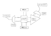
チャネルイコライザー、即ち、ゲイン平滑化デバイスは、自由空間デマックス(demux)とVOAアレイとの組合せとして製造できる。チャネルイコライザーは、回折格子や薄膜フィルターなどのデマックス素子との組合せでVOA素子を有し、これは、光学シグナルを分散させ、それによって、個々の波長が空間で分離される。一体化したVOA素子を有するDGE素子を示す例を図16に示す。
ゲル変調器の性質は自由空間なので、多重光学機能のハイブリッド統合化(マックス/デマックス(mux/demux)、スイッチアレイ及びVOAアレイ)を行ってR−OADMを構築することが可能である。
回折原理は、例えば、モニタリングアウトプットとして1次のうちの1つを使用することによって、適用をモニターするのに適しており、一方、変調器はまた、いくつかの他の光学機能を送達する。光学チャネルモニター(OCM)はまた、フィードバックシステムにおいてタップで較正した検出器を用いることによって実行し得る。
Claims (14)
- 光通信システムにおける光の変調を提供する方法であって、
当該方法は、
透明プリズムに隣接して取り付けられたゲル層又は膜を提供するステップを有し、該プリズムは、該光通信システムへ/該光通信システムから、光を送るおよび/または光を受け取るものであり、
1セットの個別にアドレス可能な電極を基板に提供するステップを有し、該電極は、該プリズムとは反対側を向いた該ゲル又は膜の表面から、適切な間隔を置いて配置されており、
各電極に励起電圧を加えるための手段を提供するステップを有し、これによって、波動パターンを該ゲル又は膜層の表面上に提供して、該ゲル又は膜層の初期状態に重畳させ、
励起電圧を除去して該ゲル又は膜層が該初期状態に戻るように、電極への励起電圧を制御するステップを有すること、
を特徴とする前記方法。 - プリズムに取り付けられた少なくとも1つの光ファイバが、光通信システムへ/光通信システムから光を提供することを特徴とする、請求項1に記載の方法。
- プリズム頭頂部の方向が基板上の電極ラインに垂直であるように、該プリズムが該基板に対して配向していることを特徴とする、請求項1に記載の方法。
- プリズム頭頂部の方向が基板上の電極ラインに並行であるように、該プリズムが該基板に対して配向していることを特徴とする、請求項1及び2に記載の方法。
- 光通信システムにおいて光を変調するためのデバイスであって、当該デバイスは、
ゲル又は膜層を有し、
光通信システムへ/光通信システムから、光を伝達するプリズムを有し、該ゲル又は膜層は、該プリズムの表面に隣接して取り付けられており、
複数の個別にアドレス可能な電極を有する基板を有し、該電極は、該プリズム表面とは反対側を向いた該ゲル又は膜層の表面からある距離を置いて位置しており、
該複数の電極の各々に制御された励起電圧を提供する駆動手段を有し、該駆動手段は波動パターンを該ゲル又は膜層の表面上に提供して、該ゲル又は膜層の初期状態に重畳させ、該駆動手段は、該励起電圧を除去した際に、該ゲル又は膜層を該初期状態に戻させる補償手段を有すること、
を特徴とする前記デバイス。 - 少なくとも1つの光ファイバが、光通信システムへ/光通信システムから、光を提供するプリズムに取り付けられていることを特徴とする、請求項5に記載のデバイス。
- プリズム頭頂部の方向が基板上の電極ラインに垂直であるように、該プリズムが該基板に対して配向していることを特徴とする、請求項5に記載のデバイス。
- プリズム頭頂部の方向が基板上の電極ラインに並行であるように、該プリズムが該基板に対して配向していることを特徴とする、請求項5に記載のデバイス。
- 駆動手段が複数の電極の各々に異なる電圧を提供することを特徴とする、請求項5に記載のデバイス。
- 駆動手段が複数の電極の各々に個別の電圧を提供することを特徴とする、請求項5に記載のデバイス。
- 電極が、等量のアドレス可能な電極を有する少なくとも3つの隣接する並行列に配置されており、それによって、ゲル層の表面上に同時に少なくとも3つの波動パターンを提供し、それによって、該ゲル層上の少なくともこれら3つの波動パターンからの反射光又は減衰光を一緒に光学的に加える手段を提供することを特徴とする、請求項5に記載のデバイス。
- 基板上の1つおきの電極が接地に接続されており、一方、他の電極が電圧を有しており、そして、該接地電極が電圧を有し、一方、他方が接地されているように配置を周期的に入れ換えることを特徴とする、請求項5に記載のデバイス。
- 駆動手段が光ダイオード又は光トランジスターを有しており、該光ダイオード又は光トランジスターが、補償手段に伝達される訂正シグナルを提供するプリズムからの光アウトプットのレベルを測定することを特徴とする、請求項5に記載のデバイス。
- 駆動手段が、複数の電極についての標的電圧のメモリーを有しており、該メモリーが、補償手段と連絡していることを特徴とする、請求項5に記載のデバイス。
Applications Claiming Priority (3)
| Application Number | Priority Date | Filing Date | Title |
|---|---|---|---|
| US40912602P | 2002-09-06 | 2002-09-06 | |
| NO20024265A NO318004B1 (no) | 2002-09-06 | 2002-09-06 | Fremgangsmate og innretning for en variabel optisk attenuator |
| PCT/NO2003/000304 WO2004023197A1 (en) | 2002-09-06 | 2003-08-29 | Method and device for variable optical attenuator |
Publications (1)
| Publication Number | Publication Date |
|---|---|
| JP2005525604A true JP2005525604A (ja) | 2005-08-25 |
Family
ID=31980710
Family Applications (1)
| Application Number | Title | Priority Date | Filing Date |
|---|---|---|---|
| JP2004533890A Pending JP2005525604A (ja) | 2002-09-06 | 2003-08-29 | 可変光減衰器の方法及びデバイス |
Country Status (6)
| Country | Link |
|---|---|
| US (1) | US6897995B2 (ja) |
| EP (1) | EP1535108A1 (ja) |
| JP (1) | JP2005525604A (ja) |
| CN (1) | CN100520485C (ja) |
| AU (1) | AU2003263690A1 (ja) |
| WO (1) | WO2004023197A1 (ja) |
Families Citing this family (13)
| Publication number | Priority date | Publication date | Assignee | Title |
|---|---|---|---|---|
| NO20033940D0 (no) * | 2003-09-05 | 2003-09-05 | Photonyx As | Fremgangsmåte og innretning for reduksjon av polariseringsavhengige effekter i en styrbar optisk komponent |
| US7133184B2 (en) * | 2004-06-03 | 2006-11-07 | Samsung Electro-Mechanics Co., Ltd. | Variable grating diffractive light modulator |
| NO326468B1 (no) * | 2005-12-06 | 2008-12-08 | Ignis Display As | Modulator med innstillbart diffraksjonsgitter (TDG) med total intern refleksjon (TIR), fremgangsmate for fremstilling av en elastomer for anvedelse deri samt anvendelse av elastomeren. |
| NO327026B1 (no) * | 2005-12-06 | 2009-04-06 | Ignis Display As | Fremgangsmate for a oke overflateledningsevnen av en polymer anvendt i en modulator med innstillbart diffraksjonsgitter (TDG) |
| NO20055796D0 (no) * | 2005-12-07 | 2005-12-07 | Ignis Photonyx As | Linjeskanningsprojeksjonsfremvisningssystem innbefattende en dobbel pixelradlysmodulator |
| WO2007081220A1 (en) * | 2006-01-13 | 2007-07-19 | Ignis Display As | Dynamic pixel structure |
| US8150267B1 (en) | 2007-04-18 | 2012-04-03 | Hewlett-Packard Development Company, L.P. | Optical interconnect |
| US8699141B2 (en) | 2009-03-13 | 2014-04-15 | Knowles Electronics, Llc | Lens assembly apparatus and method |
| US8659835B2 (en) | 2009-03-13 | 2014-02-25 | Optotune Ag | Lens systems and method |
| EP2296019A1 (en) | 2009-09-14 | 2011-03-16 | poLight AS | Optical power switch (OPS) |
| EP2322957A1 (en) | 2009-11-12 | 2011-05-18 | poLight AS | A method, device and system for reducing speckle contrast |
| JP2012156285A (ja) * | 2011-01-26 | 2012-08-16 | Fujitsu Ltd | 光増幅装置 |
| CN112933449B (zh) * | 2021-01-13 | 2022-01-21 | 安徽大学 | 一种生物压电式智能口罩及其智能控制方法 |
Family Cites Families (18)
| Publication number | Priority date | Publication date | Assignee | Title |
|---|---|---|---|---|
| CH454296A (de) * | 1967-03-17 | 1968-04-15 | Foerderung Forschung Gmbh | Einrichtung zur Verstärkung der Intensität eines optisch erzeugten Bildes |
| CH537129A (de) | 1971-10-27 | 1973-05-15 | Eidophor Ag | Projektionsvorrichtung, insbesondere für Fernsehbilder |
| US4529620A (en) | 1984-01-30 | 1985-07-16 | New York Institute Of Technology | Method of making deformable light modulator structure |
| US4635082A (en) * | 1984-05-17 | 1987-01-06 | Xerox Corporation | Thermo-optic light modulation array |
| US4900136A (en) | 1987-08-11 | 1990-02-13 | North American Philips Corporation | Method of metallizing silica-containing gel and solid state light modulator incorporating the metallized gel |
| US4857978A (en) | 1987-08-11 | 1989-08-15 | North American Philips Corporation | Solid state light modulator incorporating metallized gel and method of metallization |
| US4879602A (en) | 1987-09-04 | 1989-11-07 | New York Institute Of Technology | Electrode patterns for solid state light modulator |
| US5221747A (en) | 1989-01-19 | 1993-06-22 | Reilly Industries, Inc. | Improved process and catalyst for the preparation of 2,2' bipyridyls |
| US5116674A (en) | 1989-01-27 | 1992-05-26 | Ciba-Geigy Corporation | Composite structure |
| GB2265024B (en) * | 1992-03-14 | 1996-01-24 | British Aerospace | A spatial light modulator assembly |
| US5867301A (en) | 1996-04-22 | 1999-02-02 | Engle; Craig D. | Phase modulating device |
| WO1999009440A1 (en) | 1997-08-13 | 1999-02-25 | Foster-Miller, Inc. | Switchable optical components |
| KR100514710B1 (ko) * | 1998-01-20 | 2005-09-15 | 세이코 엡슨 가부시키가이샤 | 광 스위칭 소자, 화상 표시 장치 및 투사 장치 |
| US6369936B1 (en) * | 1999-03-12 | 2002-04-09 | Kodak Polychrome Graphics Llc | Pixel intensity control in electro-optic modulators |
| GB9930555D0 (en) | 1999-12-23 | 2000-02-16 | Opti Switch As | Optical systems |
| US6456419B1 (en) * | 2000-09-29 | 2002-09-24 | Innovative Technology Licensing, Llc | Frequency modulated liquid crystal beamsteering device |
| US6587288B2 (en) * | 2001-03-12 | 2003-07-01 | Optical Coating Laboratory, Inc. | Optical attenuation filter |
| JP2002365603A (ja) * | 2001-06-12 | 2002-12-18 | Minolta Co Ltd | 光シャッタ装置 |
-
2003
- 2003-08-29 AU AU2003263690A patent/AU2003263690A1/en not_active Abandoned
- 2003-08-29 WO PCT/NO2003/000304 patent/WO2004023197A1/en active Application Filing
- 2003-08-29 EP EP03794360A patent/EP1535108A1/en not_active Withdrawn
- 2003-08-29 JP JP2004533890A patent/JP2005525604A/ja active Pending
- 2003-09-05 US US10/656,009 patent/US6897995B2/en not_active Expired - Lifetime
- 2003-09-05 CN CNB031255574A patent/CN100520485C/zh not_active Expired - Fee Related
Also Published As
| Publication number | Publication date |
|---|---|
| EP1535108A1 (en) | 2005-06-01 |
| CN100520485C (zh) | 2009-07-29 |
| US6897995B2 (en) | 2005-05-24 |
| WO2004023197A1 (en) | 2004-03-18 |
| US20040130773A1 (en) | 2004-07-08 |
| AU2003263690A1 (en) | 2004-03-29 |
| CN1495454A (zh) | 2004-05-12 |
Similar Documents
| Publication | Publication Date | Title |
|---|---|---|
| US11243450B2 (en) | Saw modulator having optical power component for extended angular redirection of light | |
| US7085492B2 (en) | Wavelength division multiplexed device | |
| US7019883B2 (en) | Dynamic optical filter having a spatial light modulator | |
| US7352927B2 (en) | Optical add-drop multiplexer architecture with reduced effect of mirror edge diffraction | |
| EP1497682B1 (en) | Tunable optical filter | |
| US7346234B2 (en) | Reduction of MEMS mirror edge diffraction in a wavelength selective switch using servo-based multi-axes rotation | |
| CN104204916B (zh) | 光学设备与方法 | |
| EP1292857B1 (en) | Dynamically variable diffractive optical devices | |
| JP5692865B2 (ja) | 波長クロスコネクト装置 | |
| JP5730526B2 (ja) | 光スイッチ | |
| EP1400047A2 (en) | Wavelength division multiplexed device | |
| JP2005525604A (ja) | 可変光減衰器の方法及びデバイス | |
| KR20030064850A (ko) | 미세-전자기계로 재구성 가능한 광학격자 | |
| US20030206681A1 (en) | Integrating element for optical fiber communication systems based on photonic multi-bandgap quasi-crystals having optimized transfer functions | |
| JP2002267998A (ja) | 波長分散補償モジュール、光受信回路、及び光通信システム | |
| WO2001011419A9 (en) | Dynamic spectral shaping in optical fibre communication | |
| US20030206694A1 (en) | Photonic multi-bandgap lightwave device and methods for manufacturing thereof | |
| JPH03211529A (ja) | 高密度に集積化された光学的マルチプレクサ及びデマルチプレクサ | |
| WO2001086848A1 (en) | Optical wavelength division multiplexer and de-multiplexer | |
| CA2490768A1 (en) | Method and apparatus for detecting multiple optical wave lengths | |
| KR100637917B1 (ko) | 가변 광감쇄기를 위한 장치 및 방법 | |
| JP2005099800A (ja) | 光線用空間位相フィルタ、フィルタシステム及びフィルタ計算方法 | |
| KR100839335B1 (ko) | 반사형 마이크로 옵틱 간섭계형 필터 및 그 응용 장치 | |
| Yu | Optical signal processing with MEMS technology: Applications in optical communication systems | |
| TW202032931A (zh) | 分波多工雙向傳輸接取系統 |
Legal Events
| Date | Code | Title | Description |
|---|---|---|---|
| A977 | Report on retrieval |
Free format text: JAPANESE INTERMEDIATE CODE: A971007 Effective date: 20070615 |
|
| A131 | Notification of reasons for refusal |
Free format text: JAPANESE INTERMEDIATE CODE: A131 Effective date: 20071002 |
|
| A601 | Written request for extension of time |
Free format text: JAPANESE INTERMEDIATE CODE: A601 Effective date: 20071212 |
|
| A602 | Written permission of extension of time |
Free format text: JAPANESE INTERMEDIATE CODE: A602 Effective date: 20071219 |
|
| A02 | Decision of refusal |
Free format text: JAPANESE INTERMEDIATE CODE: A02 Effective date: 20080507 |