JP2005510081A - 低エネルギープラズマ強化化学蒸着法による高移動度のシリコンゲルマニウム構造体の製造方法 - Google Patents
低エネルギープラズマ強化化学蒸着法による高移動度のシリコンゲルマニウム構造体の製造方法 Download PDFInfo
- Publication number
- JP2005510081A JP2005510081A JP2003546385A JP2003546385A JP2005510081A JP 2005510081 A JP2005510081 A JP 2005510081A JP 2003546385 A JP2003546385 A JP 2003546385A JP 2003546385 A JP2003546385 A JP 2003546385A JP 2005510081 A JP2005510081 A JP 2005510081A
- Authority
- JP
- Japan
- Prior art keywords
- growth
- layer
- substrate
- substrate temperature
- lepecvd
- Prior art date
- Legal status (The legal status is an assumption and is not a legal conclusion. Google has not performed a legal analysis and makes no representation as to the accuracy of the status listed.)
- Pending
Links
- 238000000034 method Methods 0.000 title claims abstract description 44
- 238000004519 manufacturing process Methods 0.000 title claims abstract description 21
- 238000000623 plasma-assisted chemical vapour deposition Methods 0.000 title claims abstract description 15
- LEVVHYCKPQWKOP-UHFFFAOYSA-N [Si].[Ge] Chemical group [Si].[Ge] LEVVHYCKPQWKOP-UHFFFAOYSA-N 0.000 title description 5
- 239000000758 substrate Substances 0.000 claims abstract description 49
- 239000007789 gas Substances 0.000 claims abstract description 27
- 239000004065 semiconductor Substances 0.000 claims abstract description 15
- 239000002019 doping agent Substances 0.000 claims abstract description 10
- 239000012495 reaction gas Substances 0.000 claims abstract description 9
- 125000004435 hydrogen atom Chemical class [H]* 0.000 claims abstract description 8
- 239000001257 hydrogen Substances 0.000 claims abstract description 7
- 229910052739 hydrogen Inorganic materials 0.000 claims abstract description 7
- 239000000872 buffer Substances 0.000 claims description 24
- 229910052710 silicon Inorganic materials 0.000 claims description 9
- XUIMIQQOPSSXEZ-UHFFFAOYSA-N Silicon Chemical compound [Si] XUIMIQQOPSSXEZ-UHFFFAOYSA-N 0.000 claims description 8
- 239000010703 silicon Substances 0.000 claims description 8
- 230000015572 biosynthetic process Effects 0.000 claims description 7
- 239000004094 surface-active agent Substances 0.000 claims description 3
- 238000004886 process control Methods 0.000 claims description 2
- 229910000577 Silicon-germanium Inorganic materials 0.000 description 48
- 230000037230 mobility Effects 0.000 description 21
- 238000005253 cladding Methods 0.000 description 16
- 238000000038 ultrahigh vacuum chemical vapour deposition Methods 0.000 description 11
- 230000003746 surface roughness Effects 0.000 description 10
- 238000001451 molecular beam epitaxy Methods 0.000 description 9
- 229910052732 germanium Inorganic materials 0.000 description 6
- GNPVGFCGXDBREM-UHFFFAOYSA-N germanium atom Chemical compound [Ge] GNPVGFCGXDBREM-UHFFFAOYSA-N 0.000 description 5
- 238000010586 diagram Methods 0.000 description 4
- 238000004518 low pressure chemical vapour deposition Methods 0.000 description 4
- 239000000463 material Substances 0.000 description 4
- 125000004429 atom Chemical group 0.000 description 3
- 230000001419 dependent effect Effects 0.000 description 3
- 230000000694 effects Effects 0.000 description 3
- 238000010891 electric arc Methods 0.000 description 3
- 230000005525 hole transport Effects 0.000 description 3
- 239000000203 mixture Substances 0.000 description 3
- XKRFYHLGVUSROY-UHFFFAOYSA-N Argon Chemical compound [Ar] XKRFYHLGVUSROY-UHFFFAOYSA-N 0.000 description 2
- 239000013078 crystal Substances 0.000 description 2
- 230000007547 defect Effects 0.000 description 2
- 238000005516 engineering process Methods 0.000 description 2
- 238000000407 epitaxy Methods 0.000 description 2
- 238000005498 polishing Methods 0.000 description 2
- 229910008310 Si—Ge Inorganic materials 0.000 description 1
- 238000004458 analytical method Methods 0.000 description 1
- 229910052786 argon Inorganic materials 0.000 description 1
- 238000006243 chemical reaction Methods 0.000 description 1
- 230000007423 decrease Effects 0.000 description 1
- 230000001627 detrimental effect Effects 0.000 description 1
- 230000005669 field effect Effects 0.000 description 1
- 239000010408 film Substances 0.000 description 1
- 230000012447 hatching Effects 0.000 description 1
- 238000010438 heat treatment Methods 0.000 description 1
- 238000001534 heteroepitaxy Methods 0.000 description 1
- 150000002500 ions Chemical class 0.000 description 1
- 230000002045 lasting effect Effects 0.000 description 1
- 238000004377 microelectronic Methods 0.000 description 1
- 239000002243 precursor Substances 0.000 description 1
- 239000007787 solid Substances 0.000 description 1
- 238000004611 spectroscopical analysis Methods 0.000 description 1
- 239000000126 substance Substances 0.000 description 1
- 238000005979 thermal decomposition reaction Methods 0.000 description 1
- 239000010409 thin film Substances 0.000 description 1
- 230000005533 two-dimensional electron gas Effects 0.000 description 1
Images


Classifications
-
- H—ELECTRICITY
- H01—ELECTRIC ELEMENTS
- H01L—SEMICONDUCTOR DEVICES NOT COVERED BY CLASS H10
- H01L29/00—Semiconductor devices adapted for rectifying, amplifying, oscillating or switching, or capacitors or resistors with at least one potential-jump barrier or surface barrier, e.g. PN junction depletion layer or carrier concentration layer; Details of semiconductor bodies or of electrodes thereof ; Multistep manufacturing processes therefor
- H01L29/66—Types of semiconductor device ; Multistep manufacturing processes therefor
- H01L29/68—Types of semiconductor device ; Multistep manufacturing processes therefor controllable by only the electric current supplied, or only the electric potential applied, to an electrode which does not carry the current to be rectified, amplified or switched
- H01L29/76—Unipolar devices, e.g. field effect transistors
- H01L29/772—Field effect transistors
- H01L29/778—Field effect transistors with two-dimensional charge carrier gas channel, e.g. HEMT ; with two-dimensional charge-carrier layer formed at a heterojunction interface
- H01L29/7782—Field effect transistors with two-dimensional charge carrier gas channel, e.g. HEMT ; with two-dimensional charge-carrier layer formed at a heterojunction interface with confinement of carriers by at least two heterojunctions, e.g. DHHEMT, quantum well HEMT, DHMODFET
-
- H—ELECTRICITY
- H01—ELECTRIC ELEMENTS
- H01L—SEMICONDUCTOR DEVICES NOT COVERED BY CLASS H10
- H01L21/00—Processes or apparatus adapted for the manufacture or treatment of semiconductor or solid state devices or of parts thereof
- H01L21/02—Manufacture or treatment of semiconductor devices or of parts thereof
- H01L21/02104—Forming layers
- H01L21/02365—Forming inorganic semiconducting materials on a substrate
- H01L21/02367—Substrates
- H01L21/0237—Materials
- H01L21/02373—Group 14 semiconducting materials
- H01L21/02381—Silicon, silicon germanium, germanium
-
- H—ELECTRICITY
- H01—ELECTRIC ELEMENTS
- H01L—SEMICONDUCTOR DEVICES NOT COVERED BY CLASS H10
- H01L21/00—Processes or apparatus adapted for the manufacture or treatment of semiconductor or solid state devices or of parts thereof
- H01L21/02—Manufacture or treatment of semiconductor devices or of parts thereof
- H01L21/02104—Forming layers
- H01L21/02365—Forming inorganic semiconducting materials on a substrate
- H01L21/02436—Intermediate layers between substrates and deposited layers
- H01L21/02439—Materials
- H01L21/02441—Group 14 semiconducting materials
- H01L21/0245—Silicon, silicon germanium, germanium
-
- H—ELECTRICITY
- H01—ELECTRIC ELEMENTS
- H01L—SEMICONDUCTOR DEVICES NOT COVERED BY CLASS H10
- H01L21/00—Processes or apparatus adapted for the manufacture or treatment of semiconductor or solid state devices or of parts thereof
- H01L21/02—Manufacture or treatment of semiconductor devices or of parts thereof
- H01L21/02104—Forming layers
- H01L21/02365—Forming inorganic semiconducting materials on a substrate
- H01L21/02436—Intermediate layers between substrates and deposited layers
- H01L21/02494—Structure
- H01L21/02496—Layer structure
- H01L21/02502—Layer structure consisting of two layers
-
- H—ELECTRICITY
- H01—ELECTRIC ELEMENTS
- H01L—SEMICONDUCTOR DEVICES NOT COVERED BY CLASS H10
- H01L21/00—Processes or apparatus adapted for the manufacture or treatment of semiconductor or solid state devices or of parts thereof
- H01L21/02—Manufacture or treatment of semiconductor devices or of parts thereof
- H01L21/02104—Forming layers
- H01L21/02365—Forming inorganic semiconducting materials on a substrate
- H01L21/02436—Intermediate layers between substrates and deposited layers
- H01L21/02494—Structure
- H01L21/02496—Layer structure
- H01L21/0251—Graded layers
-
- H—ELECTRICITY
- H01—ELECTRIC ELEMENTS
- H01L—SEMICONDUCTOR DEVICES NOT COVERED BY CLASS H10
- H01L21/00—Processes or apparatus adapted for the manufacture or treatment of semiconductor or solid state devices or of parts thereof
- H01L21/02—Manufacture or treatment of semiconductor devices or of parts thereof
- H01L21/02104—Forming layers
- H01L21/02365—Forming inorganic semiconducting materials on a substrate
- H01L21/02518—Deposited layers
- H01L21/02521—Materials
- H01L21/02524—Group 14 semiconducting materials
- H01L21/02532—Silicon, silicon germanium, germanium
-
- H—ELECTRICITY
- H01—ELECTRIC ELEMENTS
- H01L—SEMICONDUCTOR DEVICES NOT COVERED BY CLASS H10
- H01L21/00—Processes or apparatus adapted for the manufacture or treatment of semiconductor or solid state devices or of parts thereof
- H01L21/02—Manufacture or treatment of semiconductor devices or of parts thereof
- H01L21/02104—Forming layers
- H01L21/02365—Forming inorganic semiconducting materials on a substrate
- H01L21/02612—Formation types
- H01L21/02617—Deposition types
- H01L21/0262—Reduction or decomposition of gaseous compounds, e.g. CVD
Abstract
上記仮想基板上に、Geチャンネル(55、65)と変調ドープ層(56、64、67)とを含む活性領域(14、58、68)を、低密度の低エネルギープラズマ強化化学蒸着法(LEPECVD)を用いて形成する工程で、この工程では、成長チャンバに水素(H2)を導入し、基板温度を400℃〜500℃に保持し、そして、変調ドープ層を形成するためにドーパントガスを成長チャンバにパルス状に導入する。
Description
新規の材料及び材料組成物は、例えばトランジスタのような半導体デバイスを改良するために、工業的に利用されている。これにより、集積回路(ICs)の生産スピード及びその性能を向上することができる。
B.S. Meyersonら、"Cooperative growth phenomena in Silicon/germanium low-temperature epitaxy"、Appl. Phys. Lett., Vol.53, p.2555, 1988 に報告されているように、純粋なSiは、基板温度550℃付近で、ほぼnm/minオーダーの低い成長速度である。
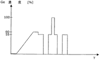
M. Arafaら、"Device and fabrication issues of high performance Si/SiGe Fets", Mat. Soc., Symp. Proc. Vol.533, p.83, 1998 に記載されているように、大きな表面粗さは、緩和現象により、いわゆるクロスハッチングの発生によって生じる。クロスハッチングの影響は、濃度勾配(傾斜率)が増加すると、さらに顕著になる。バッファ層表面のGe濃度がXf=0.3と比較的低かったとしても、丘部と溝部との高さの差は、通常は30nmである。表面粗さは、MODFET構造体の品質に有害な影響をもたらす。
P.M. Mooneyら、"SiGe technology: heteroepitaxy and high-speed microelectronics"、Annu. Rev. Mater. Sci., Vol.30, pp.335, 2000 に記載されているように、ホットウォール法は、特に高いGe濃度での制御が困難である。このように、ホットウォール法は、高移動度のホール輸送材料には適していない。従って、ホットウォール技術を利用して、純粋なGeチャンネルを含む高性能のp−MODFET構造体を形成することは不可能である。
本発明は、低エネルギープラズマ強化化学蒸着法(LEPECVD)に基づいている。
さらに、この方法は、仮想基板上に、Geチャンネルと少なくとも1つの変調ドープ層とを含む活性領域を、低密度の低エネルギープラズマ強化化学蒸着法(LEPECVD)を用いて形成する工程を含んでいる。この低密度LEPECVDは、成長チャンバに水素(H2)を導入し、基板温度は、400℃〜500℃に保持され、そして、変調ドープ層を製造するために成長チャンバにドーパントガスをパルス状に導入して行われる。
第1の処理工程のシステムパラメータは、基板温度が400℃〜850℃、ガス導入口での全反応ガス流量が5sccm〜200sccmであり、成長速度が2nm/s以上になるになるように調整される。
第2の処理工程のシステムパラメータは、基板温度を400℃〜500℃に保持するように調節されており、水素(H2)を成長チャンバに導入し、且つドーパントガスを成長チャンバ中にパルス状に導入して、少なくとも1つの層に変調ドーピングできるようにされている。
本発明は、異なった格子パラメータの材料の一方を他方の上側に成長させたときの、歪み層エキタピシーの本質的な利点をうまく利用している。例えば、ゲルマニウム(Ge)を小さい格子パラメータの基板上に析出したとき、Ge原子は、下側の原子と配列して、Geに圧縮歪みが加えられる。例えば、歪んだGeの内部では、ホールは、抵抗が低くなって、より速く移動できるようになる。この効果は、個々のデバイスの寸法を小さくすることなく、速いデバイスを実現するのに利用できる。
以下の条件の、高密度の低エネルギープラズマ強化化学蒸着法(LEPECVD)を用いて、Si基板上に仮想基板を形成する工程。仮想基板は、傾斜Si1−xGex層で0≦X≦Xfの層と、Ge濃度が一定のSi1−xGex層と、を含んでいる。この工程は、
i.成長速度が2nm/s以上
ii.基板温度が400℃〜850℃
iii.成長チャンバのガス導入口における全反応ガス流が5sccm〜200sccm
の条件で行われる。
以下の条件の、低密度の低エネルギープラズマ強化化学蒸着法(LEPECVD)を用いて、仮想基板上に活性領域を形成する工程。活性領域は、Geチャンネルと、少なくとも1つの変調ドープ層を含んでいる。この工程は、
i.成長チャンバ内に水素(H2)を導入して、界面活性剤として機能させる
ii.基板温度を400℃〜500℃に保持する
iii.成長チャンバ内にドーパントガスをパルス状に導入し、変調ドープ層を形成する
の条件を含んでいる。
Claims (19)
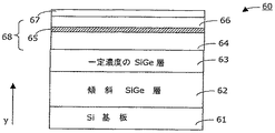
- 半導体ヘテロ構造体を、ガス導入口(26、30)を備えた成長チャンバ(23)中で製造する方法であって、上記製造方法が、
以下の条件による高密度の低エネルギープラズマ強化化学蒸着法(LEPECVD)を用いて、シリコン基板(11、51、61)上に、傾斜Si1−xGex層(12、52、62)とそれに続いてGe濃度一定のSi1−xGex層(13、53、63)とを含む仮想基板を形成する工程であって、高密度のLEPECVDの条件が、
i.成長速度が2nm/s以上、
ii.基板温度が400℃〜850℃、及び
iii.ガス導入口での全反応ガス流量が5sccm〜200sccm、の工程と、
以下の条件による低密度の低エネルギープラズマ強化化学蒸着法(LEPECVD)を用いて、上記仮想基板上に、Geチャンネル(55、65)と変調ドープ層(56、64、67)とを含む活性領域(14、58、68)を形成する工程であって、低密度のLEPECVDの条件が、
i.成長チャンバ(23)に水素(H2)を導入して、界面活性剤として機能させること、
ii.基板温度を400℃〜500℃に保持すること、及び
iii.成長チャンバ(23)にドーパントガスをパルス状に導入し、上記変調ドープ層(56、64、67)を形成すること、である工程と、
を含んでいる半導体ヘテロ構造体の製造方法。 - 上記仮想基板の形成中に、基板温度を、400℃〜800℃、好ましくは450℃〜750℃の範囲内で故意に変化させる請求項1に記載の製造方法。
- 上記活性領域(14、58、68)の形成中に、基板温度を約450℃に保持する請求項1又は2に記載の製造方法。
- ドーパントガスとしてジボランが用いられる請求項1乃至3のいずれかに記載の製造方法。
- 上記基板が約−12Vの電位を有しており、プラズマ電位がほぼ0Vである請求項1乃至4のいずれかに記載の製造方法。
- SiH4及びGeH4が、ガス導入口(26、30)から成長チャンバ(23)に導入される請求項1又は2に記載の製造方法。
- 成長速度が2nm/s〜10nm/sである請求項1又は2に記載の製造方法。
- 成長速度は、基板温度が400℃〜850℃の範囲内においては、当該基板温度にほぼ完全に依存しない請求項7に記載の製造方法。
- 成長速度は、全流量を一定にした場合には、成長チャンバ(23)内の反応ガス濃度にほぼ完全に依存しない請求項1乃至8のいずれかに記載の製造方法。
- 上記高密度の低エネルギープラズマの密度が、上記低密度の低エネルギープラズマの密度の10倍ほど大きい請求項1乃至9のいずれかに記載の製造方法。
- ヘテロ構造半導体デバイスであって、
シリコン基板(11、51、61)と、
傾斜Si1−xGex層(12、52、62)と、
Ge濃度一定のSi1−xGexバッファ層(13、53、63)と、
上記バッファ層(13、53、63)上に位置している活性領域(14、58、68)と、
4.2Kにおいて70000〜87000cm2/Vsのホール移動度を有するGeチャンネル(55、65)と、を含んでおり、
上記活性領域(14、58、68)が、少なくとも1つの変調ドープ層(56、64、67)を含む半導体デバイス。 - Si1−xGexバッファ層(13、53、63)及び/又は傾斜Si1−xGex層(12、52、62)は、RMS粗さが5nm以下である請求項11に記載の半導体デバイス。
- ガス導入口(26、30)を備えた成長チャンバ(23)を含む成長システム(80)であって、
成長システム(80)は、少なくとも2つの工程を含む低密度の低エネルギープラズマ強化化学蒸着法(LEPECVD)を行うために装備されており、これにより
第1の処理工程中のシステムパラメータが、基板温度を400℃〜850℃、ガス導入口での全反応ガス流量を5sccm〜200sccmにして、成長速度を2nm/s以上にするように調整され、
第2の処理工程中のシステムパラメータが、基板温度を400℃〜500℃に保持するように調整され、水素(H2)を成長チャンバ(23)に導入し、且つドーパントガスを成長チャンバ(23)にパルス状に導入して、少なくとも1つの層に変調ドーピングできる、成長システム。 - 上記成長システムが、処理制御ユニット(81)、好ましくは適当なソフトウェアモジュール(82、83)を備えたコンピュータを含んでおり、上記システムパラメータを適宜制御できる請求項13に記載の成長システム。
- 上記処理制御ユニット(81)は、第1の処理工程中に、基板温度を400℃〜800℃、好ましくは450℃〜750℃の範囲内で変化させることができる請求項13に記載の成長システム。
- 上記処理制御ユニット(81)は、第2の処理工程中に、基板温度を450℃に保持することができる請求項13に記載の成長システム。
- 上記処理制御ユニット(81)は、ドーパントガスであるジボランの導入を制御できる請求項13に記載の成長システム。
- 上記処理制御ユニット(81)は、電位約12ボルトの低エネルギーのプラズマと、ほぼ0Vのプラズマ電位とを維持するために、上記パラメータを制御することができる請求項13に記載の成長システム。
- 上記処理制御ユニット(81)は、SiH4及びGeH4の成長チャンバ(23)への導入を制御できる請求項13に記載の成長システム。
Applications Claiming Priority (2)
| Application Number | Priority Date | Filing Date | Title |
|---|---|---|---|
| EP01127834A EP1315199A1 (en) | 2001-11-22 | 2001-11-22 | Formation of high-mobility silicon-germanium structures by low-energy plasma enhanced chemical vapor deposition |
| PCT/EP2002/009922 WO2003044839A2 (en) | 2001-11-22 | 2002-09-05 | Formation of high-mobility silicon-germanium structures by low-energy plasma enhanced chemical vapor deposition |
Publications (2)
| Publication Number | Publication Date |
|---|---|
| JP2005510081A true JP2005510081A (ja) | 2005-04-14 |
| JP2005510081A5 JP2005510081A5 (ja) | 2006-01-05 |
Family
ID=8179316
Family Applications (1)
| Application Number | Title | Priority Date | Filing Date |
|---|---|---|---|
| JP2003546385A Pending JP2005510081A (ja) | 2001-11-22 | 2002-09-05 | 低エネルギープラズマ強化化学蒸着法による高移動度のシリコンゲルマニウム構造体の製造方法 |
Country Status (6)
| Country | Link |
|---|---|
| US (1) | US7115895B2 (ja) |
| EP (1) | EP1315199A1 (ja) |
| JP (1) | JP2005510081A (ja) |
| CN (1) | CN100345254C (ja) |
| AU (1) | AU2002335310A1 (ja) |
| WO (1) | WO2003044839A2 (ja) |
Cited By (2)
| Publication number | Priority date | Publication date | Assignee | Title |
|---|---|---|---|---|
| JP2010267969A (ja) * | 2009-05-13 | 2010-11-25 | Siltronic Ag | おもて面と裏面とを有するシリコン単結晶基板及び前記おもて面上に堆積されたSiGeの層を含んでなるウェーハを製造する方法 |
| KR20140147250A (ko) * | 2013-06-19 | 2014-12-30 | 엘지이노텍 주식회사 | 반도체 기판, 발광 소자 및 전자 소자 |
Families Citing this family (14)
| Publication number | Priority date | Publication date | Assignee | Title |
|---|---|---|---|---|
| US6855436B2 (en) * | 2003-05-30 | 2005-02-15 | International Business Machines Corporation | Formation of silicon-germanium-on-insulator (SGOI) by an integral high temperature SIMOX-Ge interdiffusion anneal |
| AU2003223991A1 (en) * | 2003-03-26 | 2004-10-18 | Eidgenoessische Technische Hochschule Zuerich | Formation of thin semiconductor layers by low-energy plasma enhanced chemical vapor deposition and semiconductor heterostructure devices |
| EP1513233B1 (en) * | 2003-09-05 | 2008-10-29 | Epispeed S.A. | InGaAs/GaAs lasers on Silicon produced by LEPECVD and MOCVD |
| EP1745165B1 (en) | 2004-04-30 | 2011-03-30 | Dichroic cell s.r.l. | Method for producing virtual ge substrates for iii/v-integration on si(001) |
| JP2007250903A (ja) * | 2006-03-16 | 2007-09-27 | Matsushita Electric Ind Co Ltd | ヘテロ接合バイポーラトランジスタおよびその製造方法 |
| EP2049939A1 (en) * | 2006-08-11 | 2009-04-22 | Paul Scherrer Institut | Light modulators comprising si-ge quantum well layers |
| JP5308336B2 (ja) | 2006-08-25 | 2013-10-09 | ブレイン アンド サイエンス エルエルシー | 被験者の特定認知感情状態を検出するシステム |
| FR2914783A1 (fr) * | 2007-04-03 | 2008-10-10 | St Microelectronics Sa | Procede de fabrication d'un dispositif a gradient de concentration et dispositif correspondant. |
| US20110017127A1 (en) * | 2007-08-17 | 2011-01-27 | Epispeed Sa | Apparatus and method for producing epitaxial layers |
| US8237126B2 (en) * | 2007-08-17 | 2012-08-07 | Csem Centre Suisse D'electronique Et De Mictrotechnique Sa | X-ray imaging device and method for the manufacturing thereof |
| TWI562195B (en) | 2010-04-27 | 2016-12-11 | Pilegrowth Tech S R L | Dislocation and stress management by mask-less processes using substrate patterning and methods for device fabrication |
| CN103165420B (zh) * | 2011-12-14 | 2015-11-18 | 中国科学院上海微系统与信息技术研究所 | 一种SiGe中嵌入超晶格制备应变Si的方法 |
| CN105632927B (zh) * | 2014-10-30 | 2018-09-07 | 中芯国际集成电路制造(上海)有限公司 | Pmos晶体管的形成方法 |
| KR102465536B1 (ko) * | 2016-06-08 | 2022-11-14 | 삼성전자주식회사 | 반도체 장치의 제조 방법 |
Family Cites Families (4)
| Publication number | Priority date | Publication date | Assignee | Title |
|---|---|---|---|---|
| EP0380077A3 (en) * | 1989-01-25 | 1990-09-12 | Hitachi, Ltd. | Transistor provided with strained germanium layer |
| US5241197A (en) * | 1989-01-25 | 1993-08-31 | Hitachi, Ltd. | Transistor provided with strained germanium layer |
| US5442205A (en) * | 1991-04-24 | 1995-08-15 | At&T Corp. | Semiconductor heterostructure devices with strained semiconductor layers |
| ATE394794T1 (de) * | 1999-03-12 | 2008-05-15 | Ibm | Ge kanal-heterostruktur mit hoher geschwindigkeit für feldeffektanordnungen |
-
2001
- 2001-11-22 EP EP01127834A patent/EP1315199A1/en not_active Withdrawn
-
2002
- 2002-09-05 JP JP2003546385A patent/JP2005510081A/ja active Pending
- 2002-09-05 CN CNB028273095A patent/CN100345254C/zh not_active Expired - Fee Related
- 2002-09-05 WO PCT/EP2002/009922 patent/WO2003044839A2/en active Application Filing
- 2002-09-05 AU AU2002335310A patent/AU2002335310A1/en not_active Abandoned
- 2002-09-05 US US10/496,245 patent/US7115895B2/en not_active Expired - Fee Related
Cited By (3)
| Publication number | Priority date | Publication date | Assignee | Title |
|---|---|---|---|---|
| JP2010267969A (ja) * | 2009-05-13 | 2010-11-25 | Siltronic Ag | おもて面と裏面とを有するシリコン単結晶基板及び前記おもて面上に堆積されたSiGeの層を含んでなるウェーハを製造する方法 |
| KR20140147250A (ko) * | 2013-06-19 | 2014-12-30 | 엘지이노텍 주식회사 | 반도체 기판, 발광 소자 및 전자 소자 |
| KR102142707B1 (ko) * | 2013-06-19 | 2020-08-07 | 엘지이노텍 주식회사 | 반도체 기판, 발광 소자 및 전자 소자 |
Also Published As
| Publication number | Publication date |
|---|---|
| AU2002335310A8 (en) | 2003-06-10 |
| WO2003044839A2 (en) | 2003-05-30 |
| AU2002335310A1 (en) | 2003-06-10 |
| WO2003044839A3 (en) | 2003-10-30 |
| EP1315199A1 (en) | 2003-05-28 |
| US7115895B2 (en) | 2006-10-03 |
| CN1615540A (zh) | 2005-05-11 |
| US20050116226A1 (en) | 2005-06-02 |
| CN100345254C (zh) | 2007-10-24 |
Similar Documents
| Publication | Publication Date | Title |
|---|---|---|
| US9934964B2 (en) | Semiconductor heterostructures having reduced dislocation pile-ups and related methods | |
| US6593625B2 (en) | Relaxed SiGe layers on Si or silicon-on-insulator substrates by ion implantation and thermal annealing | |
| US7060632B2 (en) | Methods for fabricating strained layers on semiconductor substrates | |
| TWI382456B (zh) | 鬆弛矽化鍺層的磊晶成長 | |
| US20040092085A1 (en) | Semiconductor crystal film and method for preparation thereof | |
| JP5065676B2 (ja) | 基板上に歪層を製造する方法及び層構造 | |
| JP2005510081A (ja) | 低エネルギープラズマ強化化学蒸着法による高移動度のシリコンゲルマニウム構造体の製造方法 | |
| Fitzgerald | GeSi/Si Nanostructures | |
| Seal et al. | Chemical vapor deposition growth and characterization of undoped and doped Ge and Ge 1− x C x quantum dots on Si | |
| US7678645B2 (en) | Formation of thin semiconductor layers by low-energy plasma enhanced chemical vapor deposition and semiconductor heterostructure devices | |
| Rosenblad et al. | Low Energy Plasma Enhanced Chemical Vapour Deposition-Plasma Enhanced Deposition of Epitaxial Si and Sige | |
| Rosenblad et al. | Virtual substrates for the n-and p-type Si-MODFET grown at very high rates | |
| Grimm et al. | Annealing experiments on supercritical Si1–xGex layers grown by RPCVD | |
| Hammond | The structural and electrical characterisation of SiGe heterostructures deposited on strain relaxed virtual substrates | |
| BLOWER | SPEC. GAS SOURCE FURNACE |
Legal Events
| Date | Code | Title | Description |
|---|---|---|---|
| A521 | Written amendment |
Free format text: JAPANESE INTERMEDIATE CODE: A523 Effective date: 20050816 |
|
| A621 | Written request for application examination |
Free format text: JAPANESE INTERMEDIATE CODE: A621 Effective date: 20050816 |
|
| RD03 | Notification of appointment of power of attorney |
Free format text: JAPANESE INTERMEDIATE CODE: A7423 Effective date: 20070730 |
|
| A521 | Written amendment |
Free format text: JAPANESE INTERMEDIATE CODE: A821 Effective date: 20070730 |
|
| A977 | Report on retrieval |
Free format text: JAPANESE INTERMEDIATE CODE: A971007 Effective date: 20081030 |
|
| A131 | Notification of reasons for refusal |
Free format text: JAPANESE INTERMEDIATE CODE: A131 Effective date: 20081111 |
|
| A521 | Written amendment |
Free format text: JAPANESE INTERMEDIATE CODE: A523 Effective date: 20090210 |
|
| A02 | Decision of refusal |
Free format text: JAPANESE INTERMEDIATE CODE: A02 Effective date: 20090602 |