JP2005347369A - 半導体装置およびその製造方法 - Google Patents
半導体装置およびその製造方法 Download PDFInfo
- Publication number
- JP2005347369A JP2005347369A JP2004162854A JP2004162854A JP2005347369A JP 2005347369 A JP2005347369 A JP 2005347369A JP 2004162854 A JP2004162854 A JP 2004162854A JP 2004162854 A JP2004162854 A JP 2004162854A JP 2005347369 A JP2005347369 A JP 2005347369A
- Authority
- JP
- Japan
- Prior art keywords
- chip
- leads
- semiconductor device
- semiconductor
- component
- Prior art date
- Legal status (The legal status is an assumption and is not a legal conclusion. Google has not performed a legal analysis and makes no representation as to the accuracy of the status listed.)
- Pending
Links
Images


Classifications
-
- H—ELECTRICITY
- H01—ELECTRIC ELEMENTS
- H01L—SEMICONDUCTOR DEVICES NOT COVERED BY CLASS H10
- H01L23/00—Details of semiconductor or other solid state devices
- H01L23/48—Arrangements for conducting electric current to or from the solid state body in operation, e.g. leads, terminal arrangements ; Selection of materials therefor
- H01L23/488—Arrangements for conducting electric current to or from the solid state body in operation, e.g. leads, terminal arrangements ; Selection of materials therefor consisting of soldered or bonded constructions
- H01L23/495—Lead-frames or other flat leads
- H01L23/49503—Lead-frames or other flat leads characterised by the die pad
- H01L23/4951—Chip-on-leads or leads-on-chip techniques, i.e. inner lead fingers being used as die pad
-
- H—ELECTRICITY
- H01—ELECTRIC ELEMENTS
- H01L—SEMICONDUCTOR DEVICES NOT COVERED BY CLASS H10
- H01L23/00—Details of semiconductor or other solid state devices
- H01L23/48—Arrangements for conducting electric current to or from the solid state body in operation, e.g. leads, terminal arrangements ; Selection of materials therefor
- H01L23/488—Arrangements for conducting electric current to or from the solid state body in operation, e.g. leads, terminal arrangements ; Selection of materials therefor consisting of soldered or bonded constructions
- H01L23/495—Lead-frames or other flat leads
- H01L23/49503—Lead-frames or other flat leads characterised by the die pad
- H01L23/49506—Lead-frames or other flat leads characterised by the die pad an insulative substrate being used as a diepad, e.g. ceramic, plastic
-
- H—ELECTRICITY
- H01—ELECTRIC ELEMENTS
- H01L—SEMICONDUCTOR DEVICES NOT COVERED BY CLASS H10
- H01L23/00—Details of semiconductor or other solid state devices
- H01L23/48—Arrangements for conducting electric current to or from the solid state body in operation, e.g. leads, terminal arrangements ; Selection of materials therefor
- H01L23/488—Arrangements for conducting electric current to or from the solid state body in operation, e.g. leads, terminal arrangements ; Selection of materials therefor consisting of soldered or bonded constructions
- H01L23/495—Lead-frames or other flat leads
- H01L23/49541—Geometry of the lead-frame
-
- H—ELECTRICITY
- H01—ELECTRIC ELEMENTS
- H01L—SEMICONDUCTOR DEVICES NOT COVERED BY CLASS H10
- H01L23/00—Details of semiconductor or other solid state devices
- H01L23/48—Arrangements for conducting electric current to or from the solid state body in operation, e.g. leads, terminal arrangements ; Selection of materials therefor
- H01L23/488—Arrangements for conducting electric current to or from the solid state body in operation, e.g. leads, terminal arrangements ; Selection of materials therefor consisting of soldered or bonded constructions
- H01L23/495—Lead-frames or other flat leads
- H01L23/49589—Capacitor integral with or on the leadframe
-
- H—ELECTRICITY
- H01—ELECTRIC ELEMENTS
- H01L—SEMICONDUCTOR DEVICES NOT COVERED BY CLASS H10
- H01L23/00—Details of semiconductor or other solid state devices
- H01L23/58—Structural electrical arrangements for semiconductor devices not otherwise provided for, e.g. in combination with batteries
- H01L23/60—Protection against electrostatic charges or discharges, e.g. Faraday shields
-
- H—ELECTRICITY
- H01—ELECTRIC ELEMENTS
- H01L—SEMICONDUCTOR DEVICES NOT COVERED BY CLASS H10
- H01L23/00—Details of semiconductor or other solid state devices
- H01L23/58—Structural electrical arrangements for semiconductor devices not otherwise provided for, e.g. in combination with batteries
- H01L23/64—Impedance arrangements
- H01L23/642—Capacitive arrangements
-
- H—ELECTRICITY
- H01—ELECTRIC ELEMENTS
- H01L—SEMICONDUCTOR DEVICES NOT COVERED BY CLASS H10
- H01L23/00—Details of semiconductor or other solid state devices
- H01L23/58—Structural electrical arrangements for semiconductor devices not otherwise provided for, e.g. in combination with batteries
- H01L23/64—Impedance arrangements
- H01L23/645—Inductive arrangements
-
- H—ELECTRICITY
- H01—ELECTRIC ELEMENTS
- H01L—SEMICONDUCTOR DEVICES NOT COVERED BY CLASS H10
- H01L24/00—Arrangements for connecting or disconnecting semiconductor or solid-state bodies; Methods or apparatus related thereto
- H01L24/01—Means for bonding being attached to, or being formed on, the surface to be connected, e.g. chip-to-package, die-attach, "first-level" interconnects; Manufacturing methods related thereto
- H01L24/42—Wire connectors; Manufacturing methods related thereto
- H01L24/47—Structure, shape, material or disposition of the wire connectors after the connecting process
- H01L24/49—Structure, shape, material or disposition of the wire connectors after the connecting process of a plurality of wire connectors
-
- H—ELECTRICITY
- H01—ELECTRIC ELEMENTS
- H01L—SEMICONDUCTOR DEVICES NOT COVERED BY CLASS H10
- H01L2224/00—Indexing scheme for arrangements for connecting or disconnecting semiconductor or solid-state bodies and methods related thereto as covered by H01L24/00
- H01L2224/01—Means for bonding being attached to, or being formed on, the surface to be connected, e.g. chip-to-package, die-attach, "first-level" interconnects; Manufacturing methods related thereto
- H01L2224/02—Bonding areas; Manufacturing methods related thereto
- H01L2224/04—Structure, shape, material or disposition of the bonding areas prior to the connecting process
- H01L2224/05—Structure, shape, material or disposition of the bonding areas prior to the connecting process of an individual bonding area
- H01L2224/0554—External layer
- H01L2224/0555—Shape
- H01L2224/05552—Shape in top view
- H01L2224/05554—Shape in top view being square
-
- H—ELECTRICITY
- H01—ELECTRIC ELEMENTS
- H01L—SEMICONDUCTOR DEVICES NOT COVERED BY CLASS H10
- H01L2224/00—Indexing scheme for arrangements for connecting or disconnecting semiconductor or solid-state bodies and methods related thereto as covered by H01L24/00
- H01L2224/01—Means for bonding being attached to, or being formed on, the surface to be connected, e.g. chip-to-package, die-attach, "first-level" interconnects; Manufacturing methods related thereto
- H01L2224/42—Wire connectors; Manufacturing methods related thereto
- H01L2224/44—Structure, shape, material or disposition of the wire connectors prior to the connecting process
- H01L2224/45—Structure, shape, material or disposition of the wire connectors prior to the connecting process of an individual wire connector
- H01L2224/45001—Core members of the connector
- H01L2224/45099—Material
- H01L2224/451—Material with a principal constituent of the material being a metal or a metalloid, e.g. boron (B), silicon (Si), germanium (Ge), arsenic (As), antimony (Sb), tellurium (Te) and polonium (Po), and alloys thereof
- H01L2224/45138—Material with a principal constituent of the material being a metal or a metalloid, e.g. boron (B), silicon (Si), germanium (Ge), arsenic (As), antimony (Sb), tellurium (Te) and polonium (Po), and alloys thereof the principal constituent melting at a temperature of greater than or equal to 950°C and less than 1550°C
- H01L2224/45144—Gold (Au) as principal constituent
-
- H—ELECTRICITY
- H01—ELECTRIC ELEMENTS
- H01L—SEMICONDUCTOR DEVICES NOT COVERED BY CLASS H10
- H01L2224/00—Indexing scheme for arrangements for connecting or disconnecting semiconductor or solid-state bodies and methods related thereto as covered by H01L24/00
- H01L2224/01—Means for bonding being attached to, or being formed on, the surface to be connected, e.g. chip-to-package, die-attach, "first-level" interconnects; Manufacturing methods related thereto
- H01L2224/42—Wire connectors; Manufacturing methods related thereto
- H01L2224/47—Structure, shape, material or disposition of the wire connectors after the connecting process
- H01L2224/48—Structure, shape, material or disposition of the wire connectors after the connecting process of an individual wire connector
- H01L2224/4805—Shape
- H01L2224/4809—Loop shape
- H01L2224/48091—Arched
-
- H—ELECTRICITY
- H01—ELECTRIC ELEMENTS
- H01L—SEMICONDUCTOR DEVICES NOT COVERED BY CLASS H10
- H01L2224/00—Indexing scheme for arrangements for connecting or disconnecting semiconductor or solid-state bodies and methods related thereto as covered by H01L24/00
- H01L2224/01—Means for bonding being attached to, or being formed on, the surface to be connected, e.g. chip-to-package, die-attach, "first-level" interconnects; Manufacturing methods related thereto
- H01L2224/42—Wire connectors; Manufacturing methods related thereto
- H01L2224/47—Structure, shape, material or disposition of the wire connectors after the connecting process
- H01L2224/48—Structure, shape, material or disposition of the wire connectors after the connecting process of an individual wire connector
- H01L2224/481—Disposition
- H01L2224/48151—Connecting between a semiconductor or solid-state body and an item not being a semiconductor or solid-state body, e.g. chip-to-substrate, chip-to-passive
- H01L2224/48153—Connecting between a semiconductor or solid-state body and an item not being a semiconductor or solid-state body, e.g. chip-to-substrate, chip-to-passive the body and the item being arranged next to each other, e.g. on a common substrate
- H01L2224/48195—Connecting between a semiconductor or solid-state body and an item not being a semiconductor or solid-state body, e.g. chip-to-substrate, chip-to-passive the body and the item being arranged next to each other, e.g. on a common substrate the item being a discrete passive component
-
- H—ELECTRICITY
- H01—ELECTRIC ELEMENTS
- H01L—SEMICONDUCTOR DEVICES NOT COVERED BY CLASS H10
- H01L2224/00—Indexing scheme for arrangements for connecting or disconnecting semiconductor or solid-state bodies and methods related thereto as covered by H01L24/00
- H01L2224/01—Means for bonding being attached to, or being formed on, the surface to be connected, e.g. chip-to-package, die-attach, "first-level" interconnects; Manufacturing methods related thereto
- H01L2224/42—Wire connectors; Manufacturing methods related thereto
- H01L2224/47—Structure, shape, material or disposition of the wire connectors after the connecting process
- H01L2224/48—Structure, shape, material or disposition of the wire connectors after the connecting process of an individual wire connector
- H01L2224/481—Disposition
- H01L2224/48151—Connecting between a semiconductor or solid-state body and an item not being a semiconductor or solid-state body, e.g. chip-to-substrate, chip-to-passive
- H01L2224/48221—Connecting between a semiconductor or solid-state body and an item not being a semiconductor or solid-state body, e.g. chip-to-substrate, chip-to-passive the body and the item being stacked
- H01L2224/48245—Connecting between a semiconductor or solid-state body and an item not being a semiconductor or solid-state body, e.g. chip-to-substrate, chip-to-passive the body and the item being stacked the item being metallic
- H01L2224/48247—Connecting between a semiconductor or solid-state body and an item not being a semiconductor or solid-state body, e.g. chip-to-substrate, chip-to-passive the body and the item being stacked the item being metallic connecting the wire to a bond pad of the item
-
- H—ELECTRICITY
- H01—ELECTRIC ELEMENTS
- H01L—SEMICONDUCTOR DEVICES NOT COVERED BY CLASS H10
- H01L2224/00—Indexing scheme for arrangements for connecting or disconnecting semiconductor or solid-state bodies and methods related thereto as covered by H01L24/00
- H01L2224/01—Means for bonding being attached to, or being formed on, the surface to be connected, e.g. chip-to-package, die-attach, "first-level" interconnects; Manufacturing methods related thereto
- H01L2224/42—Wire connectors; Manufacturing methods related thereto
- H01L2224/47—Structure, shape, material or disposition of the wire connectors after the connecting process
- H01L2224/48—Structure, shape, material or disposition of the wire connectors after the connecting process of an individual wire connector
- H01L2224/481—Disposition
- H01L2224/48151—Connecting between a semiconductor or solid-state body and an item not being a semiconductor or solid-state body, e.g. chip-to-substrate, chip-to-passive
- H01L2224/48221—Connecting between a semiconductor or solid-state body and an item not being a semiconductor or solid-state body, e.g. chip-to-substrate, chip-to-passive the body and the item being stacked
- H01L2224/48245—Connecting between a semiconductor or solid-state body and an item not being a semiconductor or solid-state body, e.g. chip-to-substrate, chip-to-passive the body and the item being stacked the item being metallic
- H01L2224/48253—Connecting between a semiconductor or solid-state body and an item not being a semiconductor or solid-state body, e.g. chip-to-substrate, chip-to-passive the body and the item being stacked the item being metallic connecting the wire to a potential ring of the item
-
- H—ELECTRICITY
- H01—ELECTRIC ELEMENTS
- H01L—SEMICONDUCTOR DEVICES NOT COVERED BY CLASS H10
- H01L2224/00—Indexing scheme for arrangements for connecting or disconnecting semiconductor or solid-state bodies and methods related thereto as covered by H01L24/00
- H01L2224/01—Means for bonding being attached to, or being formed on, the surface to be connected, e.g. chip-to-package, die-attach, "first-level" interconnects; Manufacturing methods related thereto
- H01L2224/42—Wire connectors; Manufacturing methods related thereto
- H01L2224/47—Structure, shape, material or disposition of the wire connectors after the connecting process
- H01L2224/49—Structure, shape, material or disposition of the wire connectors after the connecting process of a plurality of wire connectors
- H01L2224/491—Disposition
- H01L2224/4911—Disposition the connectors being bonded to at least one common bonding area, e.g. daisy chain
- H01L2224/49113—Disposition the connectors being bonded to at least one common bonding area, e.g. daisy chain the connectors connecting different bonding areas on the semiconductor or solid-state body to a common bonding area outside the body, e.g. converging wires
-
- H—ELECTRICITY
- H01—ELECTRIC ELEMENTS
- H01L—SEMICONDUCTOR DEVICES NOT COVERED BY CLASS H10
- H01L2224/00—Indexing scheme for arrangements for connecting or disconnecting semiconductor or solid-state bodies and methods related thereto as covered by H01L24/00
- H01L2224/01—Means for bonding being attached to, or being formed on, the surface to be connected, e.g. chip-to-package, die-attach, "first-level" interconnects; Manufacturing methods related thereto
- H01L2224/42—Wire connectors; Manufacturing methods related thereto
- H01L2224/47—Structure, shape, material or disposition of the wire connectors after the connecting process
- H01L2224/49—Structure, shape, material or disposition of the wire connectors after the connecting process of a plurality of wire connectors
- H01L2224/491—Disposition
- H01L2224/4912—Layout
- H01L2224/49171—Fan-out arrangements
-
- H—ELECTRICITY
- H01—ELECTRIC ELEMENTS
- H01L—SEMICONDUCTOR DEVICES NOT COVERED BY CLASS H10
- H01L2224/00—Indexing scheme for arrangements for connecting or disconnecting semiconductor or solid-state bodies and methods related thereto as covered by H01L24/00
- H01L2224/01—Means for bonding being attached to, or being formed on, the surface to be connected, e.g. chip-to-package, die-attach, "first-level" interconnects; Manufacturing methods related thereto
- H01L2224/42—Wire connectors; Manufacturing methods related thereto
- H01L2224/47—Structure, shape, material or disposition of the wire connectors after the connecting process
- H01L2224/49—Structure, shape, material or disposition of the wire connectors after the connecting process of a plurality of wire connectors
- H01L2224/491—Disposition
- H01L2224/4912—Layout
- H01L2224/49175—Parallel arrangements
-
- H—ELECTRICITY
- H01—ELECTRIC ELEMENTS
- H01L—SEMICONDUCTOR DEVICES NOT COVERED BY CLASS H10
- H01L2224/00—Indexing scheme for arrangements for connecting or disconnecting semiconductor or solid-state bodies and methods related thereto as covered by H01L24/00
- H01L2224/01—Means for bonding being attached to, or being formed on, the surface to be connected, e.g. chip-to-package, die-attach, "first-level" interconnects; Manufacturing methods related thereto
- H01L2224/42—Wire connectors; Manufacturing methods related thereto
- H01L2224/47—Structure, shape, material or disposition of the wire connectors after the connecting process
- H01L2224/49—Structure, shape, material or disposition of the wire connectors after the connecting process of a plurality of wire connectors
- H01L2224/494—Connecting portions
- H01L2224/4943—Connecting portions the connecting portions being staggered
-
- H—ELECTRICITY
- H01—ELECTRIC ELEMENTS
- H01L—SEMICONDUCTOR DEVICES NOT COVERED BY CLASS H10
- H01L2224/00—Indexing scheme for arrangements for connecting or disconnecting semiconductor or solid-state bodies and methods related thereto as covered by H01L24/00
- H01L2224/73—Means for bonding being of different types provided for in two or more of groups H01L2224/10, H01L2224/18, H01L2224/26, H01L2224/34, H01L2224/42, H01L2224/50, H01L2224/63, H01L2224/71
- H01L2224/732—Location after the connecting process
- H01L2224/73251—Location after the connecting process on different surfaces
- H01L2224/73265—Layer and wire connectors
-
- H—ELECTRICITY
- H01—ELECTRIC ELEMENTS
- H01L—SEMICONDUCTOR DEVICES NOT COVERED BY CLASS H10
- H01L2224/00—Indexing scheme for arrangements for connecting or disconnecting semiconductor or solid-state bodies and methods related thereto as covered by H01L24/00
- H01L2224/91—Methods for connecting semiconductor or solid state bodies including different methods provided for in two or more of groups H01L2224/80 - H01L2224/90
- H01L2224/92—Specific sequence of method steps
- H01L2224/922—Connecting different surfaces of the semiconductor or solid-state body with connectors of different types
- H01L2224/9222—Sequential connecting processes
- H01L2224/92242—Sequential connecting processes the first connecting process involving a layer connector
- H01L2224/92247—Sequential connecting processes the first connecting process involving a layer connector the second connecting process involving a wire connector
-
- H—ELECTRICITY
- H01—ELECTRIC ELEMENTS
- H01L—SEMICONDUCTOR DEVICES NOT COVERED BY CLASS H10
- H01L24/00—Arrangements for connecting or disconnecting semiconductor or solid-state bodies; Methods or apparatus related thereto
- H01L24/01—Means for bonding being attached to, or being formed on, the surface to be connected, e.g. chip-to-package, die-attach, "first-level" interconnects; Manufacturing methods related thereto
- H01L24/42—Wire connectors; Manufacturing methods related thereto
- H01L24/44—Structure, shape, material or disposition of the wire connectors prior to the connecting process
- H01L24/45—Structure, shape, material or disposition of the wire connectors prior to the connecting process of an individual wire connector
-
- H—ELECTRICITY
- H01—ELECTRIC ELEMENTS
- H01L—SEMICONDUCTOR DEVICES NOT COVERED BY CLASS H10
- H01L24/00—Arrangements for connecting or disconnecting semiconductor or solid-state bodies; Methods or apparatus related thereto
- H01L24/01—Means for bonding being attached to, or being formed on, the surface to be connected, e.g. chip-to-package, die-attach, "first-level" interconnects; Manufacturing methods related thereto
- H01L24/42—Wire connectors; Manufacturing methods related thereto
- H01L24/47—Structure, shape, material or disposition of the wire connectors after the connecting process
- H01L24/48—Structure, shape, material or disposition of the wire connectors after the connecting process of an individual wire connector
-
- H—ELECTRICITY
- H01—ELECTRIC ELEMENTS
- H01L—SEMICONDUCTOR DEVICES NOT COVERED BY CLASS H10
- H01L2924/00—Indexing scheme for arrangements or methods for connecting or disconnecting semiconductor or solid-state bodies as covered by H01L24/00
- H01L2924/01—Chemical elements
- H01L2924/01005—Boron [B]
-
- H—ELECTRICITY
- H01—ELECTRIC ELEMENTS
- H01L—SEMICONDUCTOR DEVICES NOT COVERED BY CLASS H10
- H01L2924/00—Indexing scheme for arrangements or methods for connecting or disconnecting semiconductor or solid-state bodies as covered by H01L24/00
- H01L2924/01—Chemical elements
- H01L2924/01006—Carbon [C]
-
- H—ELECTRICITY
- H01—ELECTRIC ELEMENTS
- H01L—SEMICONDUCTOR DEVICES NOT COVERED BY CLASS H10
- H01L2924/00—Indexing scheme for arrangements or methods for connecting or disconnecting semiconductor or solid-state bodies as covered by H01L24/00
- H01L2924/01—Chemical elements
- H01L2924/01014—Silicon [Si]
-
- H—ELECTRICITY
- H01—ELECTRIC ELEMENTS
- H01L—SEMICONDUCTOR DEVICES NOT COVERED BY CLASS H10
- H01L2924/00—Indexing scheme for arrangements or methods for connecting or disconnecting semiconductor or solid-state bodies as covered by H01L24/00
- H01L2924/01—Chemical elements
- H01L2924/01015—Phosphorus [P]
-
- H—ELECTRICITY
- H01—ELECTRIC ELEMENTS
- H01L—SEMICONDUCTOR DEVICES NOT COVERED BY CLASS H10
- H01L2924/00—Indexing scheme for arrangements or methods for connecting or disconnecting semiconductor or solid-state bodies as covered by H01L24/00
- H01L2924/01—Chemical elements
- H01L2924/01029—Copper [Cu]
-
- H—ELECTRICITY
- H01—ELECTRIC ELEMENTS
- H01L—SEMICONDUCTOR DEVICES NOT COVERED BY CLASS H10
- H01L2924/00—Indexing scheme for arrangements or methods for connecting or disconnecting semiconductor or solid-state bodies as covered by H01L24/00
- H01L2924/01—Chemical elements
- H01L2924/01033—Arsenic [As]
-
- H—ELECTRICITY
- H01—ELECTRIC ELEMENTS
- H01L—SEMICONDUCTOR DEVICES NOT COVERED BY CLASS H10
- H01L2924/00—Indexing scheme for arrangements or methods for connecting or disconnecting semiconductor or solid-state bodies as covered by H01L24/00
- H01L2924/01—Chemical elements
- H01L2924/01047—Silver [Ag]
-
- H—ELECTRICITY
- H01—ELECTRIC ELEMENTS
- H01L—SEMICONDUCTOR DEVICES NOT COVERED BY CLASS H10
- H01L2924/00—Indexing scheme for arrangements or methods for connecting or disconnecting semiconductor or solid-state bodies as covered by H01L24/00
- H01L2924/01—Chemical elements
- H01L2924/01078—Platinum [Pt]
-
- H—ELECTRICITY
- H01—ELECTRIC ELEMENTS
- H01L—SEMICONDUCTOR DEVICES NOT COVERED BY CLASS H10
- H01L2924/00—Indexing scheme for arrangements or methods for connecting or disconnecting semiconductor or solid-state bodies as covered by H01L24/00
- H01L2924/01—Chemical elements
- H01L2924/01079—Gold [Au]
-
- H—ELECTRICITY
- H01—ELECTRIC ELEMENTS
- H01L—SEMICONDUCTOR DEVICES NOT COVERED BY CLASS H10
- H01L2924/00—Indexing scheme for arrangements or methods for connecting or disconnecting semiconductor or solid-state bodies as covered by H01L24/00
- H01L2924/01—Chemical elements
- H01L2924/01082—Lead [Pb]
-
- H—ELECTRICITY
- H01—ELECTRIC ELEMENTS
- H01L—SEMICONDUCTOR DEVICES NOT COVERED BY CLASS H10
- H01L2924/00—Indexing scheme for arrangements or methods for connecting or disconnecting semiconductor or solid-state bodies as covered by H01L24/00
- H01L2924/013—Alloys
- H01L2924/014—Solder alloys
-
- H—ELECTRICITY
- H01—ELECTRIC ELEMENTS
- H01L—SEMICONDUCTOR DEVICES NOT COVERED BY CLASS H10
- H01L2924/00—Indexing scheme for arrangements or methods for connecting or disconnecting semiconductor or solid-state bodies as covered by H01L24/00
- H01L2924/06—Polymers
- H01L2924/078—Adhesive characteristics other than chemical
- H01L2924/07802—Adhesive characteristics other than chemical not being an ohmic electrical conductor
-
- H—ELECTRICITY
- H01—ELECTRIC ELEMENTS
- H01L—SEMICONDUCTOR DEVICES NOT COVERED BY CLASS H10
- H01L2924/00—Indexing scheme for arrangements or methods for connecting or disconnecting semiconductor or solid-state bodies as covered by H01L24/00
- H01L2924/095—Indexing scheme for arrangements or methods for connecting or disconnecting semiconductor or solid-state bodies as covered by H01L24/00 with a principal constituent of the material being a combination of two or more materials provided in the groups H01L2924/013 - H01L2924/0715
- H01L2924/097—Glass-ceramics, e.g. devitrified glass
- H01L2924/09701—Low temperature co-fired ceramic [LTCC]
-
- H—ELECTRICITY
- H01—ELECTRIC ELEMENTS
- H01L—SEMICONDUCTOR DEVICES NOT COVERED BY CLASS H10
- H01L2924/00—Indexing scheme for arrangements or methods for connecting or disconnecting semiconductor or solid-state bodies as covered by H01L24/00
- H01L2924/10—Details of semiconductor or other solid state devices to be connected
- H01L2924/11—Device type
- H01L2924/13—Discrete devices, e.g. 3 terminal devices
- H01L2924/1304—Transistor
- H01L2924/1306—Field-effect transistor [FET]
- H01L2924/13091—Metal-Oxide-Semiconductor Field-Effect Transistor [MOSFET]
-
- H—ELECTRICITY
- H01—ELECTRIC ELEMENTS
- H01L—SEMICONDUCTOR DEVICES NOT COVERED BY CLASS H10
- H01L2924/00—Indexing scheme for arrangements or methods for connecting or disconnecting semiconductor or solid-state bodies as covered by H01L24/00
- H01L2924/10—Details of semiconductor or other solid state devices to be connected
- H01L2924/11—Device type
- H01L2924/14—Integrated circuits
-
- H—ELECTRICITY
- H01—ELECTRIC ELEMENTS
- H01L—SEMICONDUCTOR DEVICES NOT COVERED BY CLASS H10
- H01L2924/00—Indexing scheme for arrangements or methods for connecting or disconnecting semiconductor or solid-state bodies as covered by H01L24/00
- H01L2924/15—Details of package parts other than the semiconductor or other solid state devices to be connected
- H01L2924/151—Die mounting substrate
- H01L2924/153—Connection portion
- H01L2924/1531—Connection portion the connection portion being formed only on the surface of the substrate opposite to the die mounting surface
- H01L2924/15311—Connection portion the connection portion being formed only on the surface of the substrate opposite to the die mounting surface being a ball array, e.g. BGA
-
- H—ELECTRICITY
- H01—ELECTRIC ELEMENTS
- H01L—SEMICONDUCTOR DEVICES NOT COVERED BY CLASS H10
- H01L2924/00—Indexing scheme for arrangements or methods for connecting or disconnecting semiconductor or solid-state bodies as covered by H01L24/00
- H01L2924/15—Details of package parts other than the semiconductor or other solid state devices to be connected
- H01L2924/181—Encapsulation
-
- H—ELECTRICITY
- H01—ELECTRIC ELEMENTS
- H01L—SEMICONDUCTOR DEVICES NOT COVERED BY CLASS H10
- H01L2924/00—Indexing scheme for arrangements or methods for connecting or disconnecting semiconductor or solid-state bodies as covered by H01L24/00
- H01L2924/19—Details of hybrid assemblies other than the semiconductor or other solid state devices to be connected
- H01L2924/1901—Structure
- H01L2924/1904—Component type
- H01L2924/19041—Component type being a capacitor
-
- H—ELECTRICITY
- H01—ELECTRIC ELEMENTS
- H01L—SEMICONDUCTOR DEVICES NOT COVERED BY CLASS H10
- H01L2924/00—Indexing scheme for arrangements or methods for connecting or disconnecting semiconductor or solid-state bodies as covered by H01L24/00
- H01L2924/19—Details of hybrid assemblies other than the semiconductor or other solid state devices to be connected
- H01L2924/1901—Structure
- H01L2924/1904—Component type
- H01L2924/19042—Component type being an inductor
-
- H—ELECTRICITY
- H01—ELECTRIC ELEMENTS
- H01L—SEMICONDUCTOR DEVICES NOT COVERED BY CLASS H10
- H01L2924/00—Indexing scheme for arrangements or methods for connecting or disconnecting semiconductor or solid-state bodies as covered by H01L24/00
- H01L2924/19—Details of hybrid assemblies other than the semiconductor or other solid state devices to be connected
- H01L2924/1901—Structure
- H01L2924/1904—Component type
- H01L2924/19043—Component type being a resistor
-
- H—ELECTRICITY
- H01—ELECTRIC ELEMENTS
- H01L—SEMICONDUCTOR DEVICES NOT COVERED BY CLASS H10
- H01L2924/00—Indexing scheme for arrangements or methods for connecting or disconnecting semiconductor or solid-state bodies as covered by H01L24/00
- H01L2924/19—Details of hybrid assemblies other than the semiconductor or other solid state devices to be connected
- H01L2924/191—Disposition
- H01L2924/19101—Disposition of discrete passive components
- H01L2924/19105—Disposition of discrete passive components in a side-by-side arrangement on a common die mounting substrate
-
- H—ELECTRICITY
- H01—ELECTRIC ELEMENTS
- H01L—SEMICONDUCTOR DEVICES NOT COVERED BY CLASS H10
- H01L2924/00—Indexing scheme for arrangements or methods for connecting or disconnecting semiconductor or solid-state bodies as covered by H01L24/00
- H01L2924/19—Details of hybrid assemblies other than the semiconductor or other solid state devices to be connected
- H01L2924/191—Disposition
- H01L2924/19101—Disposition of discrete passive components
- H01L2924/19107—Disposition of discrete passive components off-chip wires
-
- H—ELECTRICITY
- H01—ELECTRIC ELEMENTS
- H01L—SEMICONDUCTOR DEVICES NOT COVERED BY CLASS H10
- H01L2924/00—Indexing scheme for arrangements or methods for connecting or disconnecting semiconductor or solid-state bodies as covered by H01L24/00
- H01L2924/30—Technical effects
- H01L2924/301—Electrical effects
- H01L2924/30105—Capacitance
-
- H—ELECTRICITY
- H01—ELECTRIC ELEMENTS
- H01L—SEMICONDUCTOR DEVICES NOT COVERED BY CLASS H10
- H01L2924/00—Indexing scheme for arrangements or methods for connecting or disconnecting semiconductor or solid-state bodies as covered by H01L24/00
- H01L2924/30—Technical effects
- H01L2924/301—Electrical effects
- H01L2924/30107—Inductance
Abstract
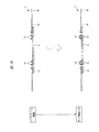
【解決手段】 半導体チップ3と、半導体チップ3の周囲に配置された複数のインナリード5aと、インナリード5aの端部と絶縁性の接着剤を介して接続し、かつ半導体チップ3と接着剤を介して接続するシート部材8と、それぞれインナリード5aに一体で繋がる複数のアウタリード5bと、半導体チップ3のパッド3cと複数のインナリード5aとをそれぞれ接続する複数のワイヤ6と、半導体チップ3と複数のインナリード5aとの間の領域において複数のインナリード5aのリード列に沿って配置されたバーリード5cとを有し、表面実装部品であるチップ部品が、半導体チップ3と複数のインナリード5aとの間の領域において、ワイヤ6の下部に配置されているとともに、バーリード5c上に搭載されており、チップ部品を有するQFP1の小型化を図ることができる。
【選択図】 図1
Description
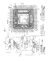
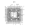
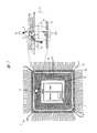
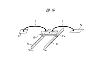
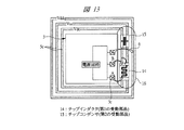
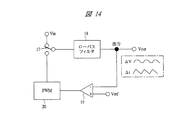
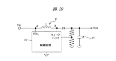
図1は本発明の実施の形態1の半導体装置の構造の一例を封止体を透過して示す平面図およびチップ部品の拡大接続図、図2は図1に示すZ部のチップ部品の構成図、図3は図1に示すZ部のチップ部品の変形例の構成図、図4は本発明の実施の形態1の変形例の半導体装置の構造を封止体を透過して示す平面図、図5は本発明の実施の形態1の変形例の半導体装置の構造を封止体を透過して示す平面図およびチップ部品の拡大接続図、図6は図5に示すチップ部品の接続状態を示す構成図、図7は本発明の実施の形態1の変形例の半導体装置の構造を封止体を透過して示す平面図およびチップ部品の拡大接続図、図8は本発明の実施の形態1の変形例の半導体装置の構造を封止体を透過して示す平面図およびチップ部品の拡大接続図、図9は本発明の実施の形態1の変形例の半導体装置の構造を封止体を透過して示す拡大部分平面図、図10は図9に示すチップ部品の接続状態を示す構成図、図11は図10に示すチップ部品の回路図および特性図、図12は図10に示す他のチップ部品の回路図、図13は本発明の実施の形態1の変形例の半導体装置におけるチップ部品の接続状態を示す平面図、図14は図13に示す半導体装置の回路構成を示す回路ブロック図、図15は図14に示す回路構成における降圧回路の一例を示す回路接続図、図16は図15に示す降圧回路の一例を用いた等価回路図、図17は図16に示す回路構成における回路接続図、図18は図15に示す降圧回路の変形例を用いた等価回路図、図19は図18に示す回路構成における回路接続図、図20は図14に示す回路構成における昇圧回路の一例を示す回路接続図、図21は図20に示す昇圧回路の一例を用いた等価回路図、図22は図21に示す回路構成における回路接続図、図23は図1に示す半導体装置の組み立てにおけるリードフレームの構造とチップ部品付け状態の一例を示す平面図、図24は図1に示す半導体装置の組み立てにおけるダイボンディング完了時の構造の一例を示す平面図、図25は図1に示す半導体装置の組み立てにおけるワイヤボンディング完了時と樹脂封止完了時の構造の一例を示す平面図、図26は図1に示す半導体装置の組み立てにおけるリードフレームの構造とチップ部品付け状態の一例を示す断面図、図27は図1に示す半導体装置の組み立てにおけるダイボンディング完了時の構造の一例を示す断面図、図28は図1に示す半導体装置の組み立てにおけるワイヤボンディング完了時と樹脂封止完了時の構造の一例を示す断面図である。
図29は本発明の実施の形態2の半導体装置の構造の一例を示す断面図、図30は図29に示す半導体装置においてチップ部品が搭載されていない箇所を切断した構造の一例を示す断面図、図31は本発明の実施の形態2の変形例の半導体装置の構造を示す断面図である。
2 チップコンデンサ(チップ部品)
2a 主面
2b 電極
3 半導体チップ
3a 主面
3b 裏面
3c パッド(電極)
4 銀ペースト
5 リードフレーム
5a インナリード(リード)
5b アウタリード(リード)
5c バーリード(共通リード)
6 ワイヤ
7 封止体
7a 裏面
8 シート部材
9 チップインダクタ(チップ部品)
10 チップ抵抗(チップ部品)
11 チップ抵抗(チップ部品)
11a 電極
11b 裏面
12 アンテナチップ(チップ部品)
12a アンテナ素子
12b 送受信回路
12c 充電制御系
13 チップダイオード(チップ部品)
13a ダイオード(ESD素子)
14 チップインダクタ(第1の受動部品)
15 チップコンデンサ(第2の受動部品)
16 LCフィルタ
17 SW
18 ローパスフィルタ
19 エラーアンプ
20 PWM
21 制御回路
22 トランジスタ
23 内部回路
24 フラッシュメモリ
25 絶縁性接着剤
26 QFN(半導体装置)
27 半田めっき部
28 絶縁性接着剤
Claims (19)
- 複数のリードと、
前記複数のリードそれぞれの端部と接続するシート部材と、
その主面に半導体素子および複数の電極を有しており、前記複数のリードの内側に配置され、さらに前記シート部材と接続する半導体チップと、
前記半導体チップの電極と前記複数のリードとをそれぞれ電気的に接続する導電性の複数のワイヤと、
前記半導体チップと前記複数のリードとの間の領域において前記ワイヤの下部に配置された表面実装部品であるチップ部品とを有することを特徴とする半導体装置。 - 請求項1記載の半導体装置において、前記半導体チップと前記複数のリードとの間の領域に1本または複数の共通リードが前記複数のリードのリード列に沿って配置され、前記共通リード上に前記チップ部品が搭載されていることを特徴とする半導体装置。
- 請求項2記載の半導体装置において、前記チップ部品は、前記共通リードと半田接続で電気的に接続されていることを特徴とする半導体装置。
- 請求項2記載の半導体装置において、前記チップ部品は、前記共通リードと絶縁性接着剤を介して接続されていることを特徴とする半導体装置。
- 請求項1記載の半導体装置において、前記半導体チップと前記複数のリードとの間の領域に複数の共通リードが前記複数のリードのリード列に沿って配置されており、さらに前記複数の共通リードのうち最も内側に配置された共通リードと前記半導体チップとの間の領域に前記チップ部品が配置されていることを特徴とする半導体装置。
- 請求項1記載の半導体装置において、前記チップ部品は、抵抗素子、インダクタ素子およびコンデンサ素子の何れかを有していることを特徴とする半導体装置。
- 請求項1記載の半導体装置において、前記チップ部品は、ESD保護素子を有していることを特徴とする半導体装置。
- 請求項1記載の半導体装置において、前記チップ部品は、EMC保護素子を有していることを特徴とする半導体装置。
- 請求項1記載の半導体装置において、前記チップ部品は、バイパスコンデンサ素子を有していることを特徴とする半導体装置。
- 請求項1記載の半導体装置において、前記チップ部品は、ダンピング抵抗素子を有していることを特徴とする半導体装置。
- 複数のリードと、
前記複数のリードそれぞれの端部と接続するシート部材と、
その主面に半導体素子および複数の電極を有しており、前記複数のリードの内側に配置され、さらに前記シート部材と接続する半導体チップと、
前記半導体チップの電極と前記複数のリードとをそれぞれ電気的に接続する導電性の複数のワイヤと、
前記半導体チップおよび前記複数のワイヤを封止する封止体と、
前記半導体チップの外部で、かつ前記封止体の内部に配置されており、インダクタ素子を備えた第1の受動部品とを有することを特徴とする半導体装置。 - 請求項11記載の半導体装置において、コンデンサ素子を有する第2の受動部品が前記半導体チップの外部で、かつ前記封止体の内部に配置されており、前記第1の受動部品と前記第2の受動部品とを含む降圧回路を有していることを特徴とする半導体装置。
- 請求項11記載の半導体装置において、コンデンサ素子を有する第2の受動部品が前記半導体チップの外部で、かつ前記封止体の内部に配置されており、前記第1の受動部品と前記第2の受動部品とを含む昇圧回路を有していることを特徴とする半導体装置。
- 請求項11記載の半導体装置において、コンデンサ素子を有する第2の受動部品が前記半導体チップの外部で、かつ前記封止体の内部に配置されており、前記半導体チップと前記複数のリードとの間の領域に1本または複数の共通リードが前記複数のリードのリード列に沿って配置され、前記共通リード上に前記第1および第2の受動部品が搭載されていることを特徴とする半導体装置。
- 請求項11記載の半導体装置において、コンデンサ素子を有する第2の受動部品が前記半導体チップの外部で、かつ前記封止体の内部に配置されており、前記半導体チップと前記複数のリードとの間の領域に複数の共通リードが前記複数のリードのリード列に沿って配置されており、さらに前記複数の共通リードのうち最も内側に配置された共通リードと前記半導体チップとの間の領域に前記第1および第2の受動部品が配置されていることを特徴とする半導体装置。
- 複数のリードと、前記複数のリードの端部に接合するシート部材とを有するリードフレームを用いて組み立てられる半導体装置の製造方法であって、
(a)前記シート部材と前記複数のリードの端部とが絶縁性接着剤を介して接合された前記リードフレームを準備する工程と、
(b)前記シート部材におけるチップ搭載部の外側で、かつ前記複数のリードより内側の領域に表面実装部品であるチップ部品を搭載する工程と、
(c)前記(b)工程の後、前記シート部材の前記チップ搭載部に半導体チップを搭載する工程と、
(d)前記半導体チップの主面の複数の電極と前記複数のリードそれぞれを導電性の複数のワイヤでそれぞれ電気的に接続する工程と、
(e)前記半導体チップおよび前記複数のリードを樹脂封止して封止体を形成する工程と、
(f)前記リードフレームから前記複数のリードを分離して個片化する工程とを有することを特徴とする半導体装置の製造方法。 - 請求項16記載の半導体装置の製造方法において、前記(a)工程で、前記シート部材の前記チップ搭載部の外側で、かつ前記複数のリードより内側の領域に、前記複数のリードのリード列に沿って1本または複数の共通リードが配置された前記リードフレームを準備した後、前記(b)工程で、前記共通リード上に前記チップ部品を搭載することを特徴とする半導体装置の製造方法。
- 請求項16記載の半導体装置の製造方法において、前記(b)工程で、銀ペーストを介して前記チップ部品を搭載し、前記搭載後、ベーク処理を行うことを特徴とする半導体装置の製造方法。
- 請求項16記載の半導体装置の製造方法において、前記(b)工程で、半田ペーストを介して前記チップ部品を搭載し、前記搭載後、リフロー処理を行うことを特徴とする半導体装置の製造方法。
Priority Applications (2)
| Application Number | Priority Date | Filing Date | Title |
|---|---|---|---|
| JP2004162854A JP2005347369A (ja) | 2004-06-01 | 2004-06-01 | 半導体装置およびその製造方法 |
| US11/140,394 US20050263863A1 (en) | 2004-06-01 | 2005-05-31 | Semiconductor device and a method of manufacturing the same |
Applications Claiming Priority (1)
| Application Number | Priority Date | Filing Date | Title |
|---|---|---|---|
| JP2004162854A JP2005347369A (ja) | 2004-06-01 | 2004-06-01 | 半導体装置およびその製造方法 |
Publications (2)
| Publication Number | Publication Date |
|---|---|
| JP2005347369A true JP2005347369A (ja) | 2005-12-15 |
| JP2005347369A5 JP2005347369A5 (ja) | 2007-07-12 |
Family
ID=35424258
Family Applications (1)
| Application Number | Title | Priority Date | Filing Date |
|---|---|---|---|
| JP2004162854A Pending JP2005347369A (ja) | 2004-06-01 | 2004-06-01 | 半導体装置およびその製造方法 |
Country Status (2)
| Country | Link |
|---|---|
| US (1) | US20050263863A1 (ja) |
| JP (1) | JP2005347369A (ja) |
Cited By (2)
| Publication number | Priority date | Publication date | Assignee | Title |
|---|---|---|---|---|
| JP2007173712A (ja) * | 2005-12-26 | 2007-07-05 | Hitachi Metals Ltd | Dc−dcコンバータ |
| JP2020113656A (ja) * | 2019-01-11 | 2020-07-27 | 株式会社デンソー | 電子装置およびその製造方法 |
Families Citing this family (11)
| Publication number | Priority date | Publication date | Assignee | Title |
|---|---|---|---|---|
| US20060220191A1 (en) * | 2005-04-01 | 2006-10-05 | Honeywell International Inc. | Electronic package with a stepped-pitch leadframe |
| MY145348A (en) * | 2007-03-15 | 2012-01-31 | Semiconductor Components Ind | Circuit component and method of manufacture |
| US8824165B2 (en) * | 2008-02-18 | 2014-09-02 | Cyntec Co. Ltd | Electronic package structure |
| KR100954981B1 (ko) * | 2008-03-31 | 2010-04-29 | 권구만 | 다양한 지형선택이 가능한 골프연습기구 |
| US7847391B2 (en) * | 2008-07-01 | 2010-12-07 | Texas Instruments Incorporated | Manufacturing method for integrating a shunt resistor into a semiconductor package |
| US8241965B2 (en) * | 2009-10-01 | 2012-08-14 | Stats Chippac Ltd. | Integrated circuit packaging system with pad connection and method of manufacture thereof |
| JP5341717B2 (ja) * | 2009-11-10 | 2013-11-13 | ルネサスエレクトロニクス株式会社 | 半導体パッケージ及びシステム |
| JP2013110314A (ja) * | 2011-11-22 | 2013-06-06 | Elpida Memory Inc | 半導体装置 |
| US11342260B2 (en) * | 2019-10-15 | 2022-05-24 | Win Semiconductors Corp. | Power flat no-lead package |
| US11380631B2 (en) * | 2019-11-27 | 2022-07-05 | Texas Instruments Incorporated | Lead frame for multi-chip modules with integrated surge protection |
| DE102022200892A1 (de) | 2022-01-27 | 2023-07-27 | Robert Bosch Gesellschaft mit beschränkter Haftung | Spannungswandler und Spannungswandlermodul |
Family Cites Families (13)
| Publication number | Priority date | Publication date | Assignee | Title |
|---|---|---|---|---|
| US4705917A (en) * | 1985-08-27 | 1987-11-10 | Hughes Aircraft Company | Microelectronic package |
| US5089878A (en) * | 1989-06-09 | 1992-02-18 | Lee Jaesup N | Low impedance packaging |
| JP3137749B2 (ja) * | 1992-06-30 | 2001-02-26 | 株式会社日立製作所 | 半導体集積回路装置 |
| US5457340A (en) * | 1992-12-07 | 1995-10-10 | Integrated Device Technology, Inc. | Leadframe with power and ground planes |
| JPH06283650A (ja) * | 1993-03-26 | 1994-10-07 | Ibiden Co Ltd | 半導体装置 |
| US5343074A (en) * | 1993-10-04 | 1994-08-30 | Motorola, Inc. | Semiconductor device having voltage distribution ring(s) and method for making the same |
| US6462404B1 (en) * | 1997-02-28 | 2002-10-08 | Micron Technology, Inc. | Multilevel leadframe for a packaged integrated circuit |
| US6476486B1 (en) * | 1997-10-30 | 2002-11-05 | Agilent Technologies, Inc. | Ball grid array package with supplemental electronic component |
| TW488054B (en) * | 2001-06-22 | 2002-05-21 | Advanced Semiconductor Eng | Semiconductor package for integrating surface mount devices |
| JP4010792B2 (ja) * | 2001-10-19 | 2007-11-21 | 株式会社ルネサステクノロジ | 半導体装置 |
| US7002249B2 (en) * | 2002-11-12 | 2006-02-21 | Primarion, Inc. | Microelectronic component with reduced parasitic inductance and method of fabricating |
| US6903448B1 (en) * | 2002-11-12 | 2005-06-07 | Marvell International Ltd. | High performance leadframe in electronic package |
| US7253506B2 (en) * | 2003-06-23 | 2007-08-07 | Power-One, Inc. | Micro lead frame package |
-
2004
- 2004-06-01 JP JP2004162854A patent/JP2005347369A/ja active Pending
-
2005
- 2005-05-31 US US11/140,394 patent/US20050263863A1/en not_active Abandoned
Cited By (3)
| Publication number | Priority date | Publication date | Assignee | Title |
|---|---|---|---|---|
| JP2007173712A (ja) * | 2005-12-26 | 2007-07-05 | Hitachi Metals Ltd | Dc−dcコンバータ |
| JP2020113656A (ja) * | 2019-01-11 | 2020-07-27 | 株式会社デンソー | 電子装置およびその製造方法 |
| JP7172617B2 (ja) | 2019-01-11 | 2022-11-16 | 株式会社デンソー | 電子装置およびその製造方法 |
Also Published As
| Publication number | Publication date |
|---|---|
| US20050263863A1 (en) | 2005-12-01 |
Similar Documents
| Publication | Publication Date | Title |
|---|---|---|
| US20050263863A1 (en) | Semiconductor device and a method of manufacturing the same | |
| KR101086751B1 (ko) | 반도체 장치 및 전원 시스템 | |
| US8153473B2 (en) | Module having a stacked passive element and method of forming the same | |
| TWI385778B (zh) | 具有堆疊分立電感器結構的半導體功率裝置 | |
| CN101990709B (zh) | 层叠的功率转换器结构和方法 | |
| US9054086B2 (en) | Module having a stacked passive element and method of forming the same | |
| USRE41869E1 (en) | Semiconductor device | |
| US7482699B2 (en) | Semiconductor device | |
| CN107403794B (zh) | 包括倒装地安装的ic和垂直集成的电感器的半导体封装体 | |
| US8362626B2 (en) | Semiconductor device with non-overlapped circuits | |
| US20080135991A1 (en) | Semiconductor device package featuring encapsulated leadframe with projecting bumps or balls | |
| JP2007500441A (ja) | ワイヤボンドボールグリッドアレイ用グランドアーチ | |
| US8063472B2 (en) | Semiconductor package with stacked dice for a buck converter | |
| US9029995B2 (en) | Semiconductor device and method of manufacturing the same | |
| JP4885635B2 (ja) | 半導体装置 | |
| US5907184A (en) | Integrated circuit package electrical enhancement | |
| US20200211760A1 (en) | Molded inductor with magnetic core having mold flow enhancing channels | |
| JP6414602B2 (ja) | 複合電子部品およびdcdcコンバータモジュール | |
| JP2010219244A (ja) | 半導体装置及び半導体装置製造方法 | |
| JP2008251901A (ja) | 複合半導体装置 | |
| US5763945A (en) | Integrated circuit package electrical enhancement with improved lead frame design | |
| CN107393881B (zh) | 具有集成的电感器的ic封装体 | |
| JP2010098256A (ja) | 半導体装置及び半導体装置製造方法 | |
| CN112397473A (zh) | 具有集成多抽头阻抗结构的封装体 | |
| CN113474860A (zh) | 具有用于降低的emi的集成屏蔽拓扑结构的隔离变压器 |
Legal Events
| Date | Code | Title | Description |
|---|---|---|---|
| A521 | Request for written amendment filed |
Free format text: JAPANESE INTERMEDIATE CODE: A523 Effective date: 20070525 |
|
| A621 | Written request for application examination |
Free format text: JAPANESE INTERMEDIATE CODE: A621 Effective date: 20070525 |
|
| A977 | Report on retrieval |
Free format text: JAPANESE INTERMEDIATE CODE: A971007 Effective date: 20090914 |
|
| A131 | Notification of reasons for refusal |
Free format text: JAPANESE INTERMEDIATE CODE: A131 Effective date: 20090924 |
|
| A02 | Decision of refusal |
Free format text: JAPANESE INTERMEDIATE CODE: A02 Effective date: 20100202 |