JP2005317912A - 配線基板及びこれを用いた入力装置とその製造方法 - Google Patents
配線基板及びこれを用いた入力装置とその製造方法 Download PDFInfo
- Publication number
- JP2005317912A JP2005317912A JP2004376047A JP2004376047A JP2005317912A JP 2005317912 A JP2005317912 A JP 2005317912A JP 2004376047 A JP2004376047 A JP 2004376047A JP 2004376047 A JP2004376047 A JP 2004376047A JP 2005317912 A JP2005317912 A JP 2005317912A
- Authority
- JP
- Japan
- Prior art keywords
- wiring board
- conductive layer
- substrate
- bent
- portions
- Prior art date
- Legal status (The legal status is an assumption and is not a legal conclusion. Google has not performed a legal analysis and makes no representation as to the accuracy of the status listed.)
- Pending
Links
Images


Abstract
【解決手段】複数の配線パターン22〜25及び接続部22A〜25Aが上面のみに形成されると共に可撓性を有する折曲部P−Pを有し、この折曲部P−Pで折曲げると、折曲げられる側の接続部24A、25Aが下面に配置されるようにして配線基板20を構成するものである。
【選択図】図3
Description
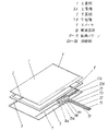
図1は本発明の一実施の形態によるタッチパネルの分解斜視図、図2は同上下基板の平面図、図3は同配線基板の平面図であり、同図において、1はポリエチレンテレフタレートやポリカーボネートフィルム等の光透過性の上基板で、この下面全面には、酸化インジウム錫や酸化錫等の光透過性の上導電層2が真空スパッタ等によって形成されている。
18A、18B 切り欠き
20 配線基板
22、23、24、25 配線パターン
22A、23A、24A、25A 接続部
26 切込み部
28 粘着部
P−P 折曲部
Claims (6)
- 複数の配線パターン及び接続部が上面のみに形成されると共に可撓性を有する折曲部を有し、この折曲部で折曲げると、一部の接続部が下面に配置される配線基板。
- 折曲後の接続部の位置を決める複数の穴を設けた請求項1記載の配線基板。
- 折曲げられず上面側に配置される接続部と、折曲げられ下面側に配置される接続部の各接続部を含む配線基板部を同等の厚さとした請求項1記載の配線基板。
- 複数の接続部の間に切込み部を設けた請求項1記載の配線基板。
- 請求項1記載の配線基板と、下面の全面又は所定の箇所に上導電層及びこの上導電層に接続された上電極が形成された上基板と、上面の全面又は所定の箇所に上記上導電層と所定の間隙を空けて対向する下導電層及びこの下導電層に接続された下電極が形成された下基板からなり、上記配線基板の複数の接続部が上記上電極及び下電極の所定の箇所に接続された入力装置。
- 配線基板を折曲部で折曲げた後、この配線基板の複数の接続部を対向配置した上下基板の上電極及び下電極の、所定の箇所に接続する請求項3記載の入力装置の製造方法。
Priority Applications (1)
| Application Number | Priority Date | Filing Date | Title |
|---|---|---|---|
| JP2004376047A JP2005317912A (ja) | 2004-02-26 | 2004-12-27 | 配線基板及びこれを用いた入力装置とその製造方法 |
Applications Claiming Priority (3)
| Application Number | Priority Date | Filing Date | Title |
|---|---|---|---|
| JP2004051085 | 2004-02-26 | ||
| JP2004109787 | 2004-04-02 | ||
| JP2004376047A JP2005317912A (ja) | 2004-02-26 | 2004-12-27 | 配線基板及びこれを用いた入力装置とその製造方法 |
Publications (2)
| Publication Number | Publication Date |
|---|---|
| JP2005317912A true JP2005317912A (ja) | 2005-11-10 |
| JP2005317912A5 JP2005317912A5 (ja) | 2007-10-18 |
Family
ID=35444973
Family Applications (1)
| Application Number | Title | Priority Date | Filing Date |
|---|---|---|---|
| JP2004376047A Pending JP2005317912A (ja) | 2004-02-26 | 2004-12-27 | 配線基板及びこれを用いた入力装置とその製造方法 |
Country Status (1)
| Country | Link |
|---|---|
| JP (1) | JP2005317912A (ja) |
Cited By (6)
| Publication number | Priority date | Publication date | Assignee | Title |
|---|---|---|---|---|
| JP2007287656A (ja) * | 2006-04-17 | 2007-11-01 | Jensin Internatl Technology Corp | 交換可能なアウトレットジョイントを備えた薄膜スイッチ |
| JP2009252896A (ja) * | 2008-04-03 | 2009-10-29 | Hitachi Chem Co Ltd | プリント配線板用硬化性樹脂組成物 |
| JP2010003749A (ja) * | 2008-06-18 | 2010-01-07 | Sony Corp | フレキシブルプリント配線板、タッチパネル、表示パネルおよび表示装置 |
| JP2011124332A (ja) * | 2009-12-09 | 2011-06-23 | Hosiden Corp | フレキシブル配線基板 |
| WO2011102152A1 (ja) * | 2010-02-17 | 2011-08-25 | シャープ株式会社 | 基板セット、電子機器、基板セットの製造方法 |
| JP2013033549A (ja) * | 2012-11-13 | 2013-02-14 | Japan Display East Co Ltd | 表示装置 |
Citations (4)
| Publication number | Priority date | Publication date | Assignee | Title |
|---|---|---|---|---|
| JPS4954747U (ja) * | 1972-08-24 | 1974-05-15 | ||
| JPS6422072U (ja) * | 1987-07-30 | 1989-02-03 | ||
| JP2000020226A (ja) * | 1998-07-06 | 2000-01-21 | Alps Electric Co Ltd | 座標入力装置 |
| JP2003207800A (ja) * | 2002-01-16 | 2003-07-25 | Alps Electric Co Ltd | Lcd電極端子の接続構造 |
-
2004
- 2004-12-27 JP JP2004376047A patent/JP2005317912A/ja active Pending
Patent Citations (4)
| Publication number | Priority date | Publication date | Assignee | Title |
|---|---|---|---|---|
| JPS4954747U (ja) * | 1972-08-24 | 1974-05-15 | ||
| JPS6422072U (ja) * | 1987-07-30 | 1989-02-03 | ||
| JP2000020226A (ja) * | 1998-07-06 | 2000-01-21 | Alps Electric Co Ltd | 座標入力装置 |
| JP2003207800A (ja) * | 2002-01-16 | 2003-07-25 | Alps Electric Co Ltd | Lcd電極端子の接続構造 |
Cited By (8)
| Publication number | Priority date | Publication date | Assignee | Title |
|---|---|---|---|---|
| JP2007287656A (ja) * | 2006-04-17 | 2007-11-01 | Jensin Internatl Technology Corp | 交換可能なアウトレットジョイントを備えた薄膜スイッチ |
| JP2009252896A (ja) * | 2008-04-03 | 2009-10-29 | Hitachi Chem Co Ltd | プリント配線板用硬化性樹脂組成物 |
| JP2010003749A (ja) * | 2008-06-18 | 2010-01-07 | Sony Corp | フレキシブルプリント配線板、タッチパネル、表示パネルおよび表示装置 |
| US8519271B2 (en) | 2008-06-18 | 2013-08-27 | Sony Corporation | Flexible printed circuit, touch panel, display panel and display |
| JP2011124332A (ja) * | 2009-12-09 | 2011-06-23 | Hosiden Corp | フレキシブル配線基板 |
| KR101760514B1 (ko) * | 2009-12-09 | 2017-07-21 | 호시덴 가부시기가이샤 | 플렉시블 배선기판 |
| WO2011102152A1 (ja) * | 2010-02-17 | 2011-08-25 | シャープ株式会社 | 基板セット、電子機器、基板セットの製造方法 |
| JP2013033549A (ja) * | 2012-11-13 | 2013-02-14 | Japan Display East Co Ltd | 表示装置 |
Similar Documents
| Publication | Publication Date | Title |
|---|---|---|
| JP4591157B2 (ja) | 配線基板及びこれを用いた入力装置とその製造方法 | |
| US7108515B2 (en) | Wiring board with bending section | |
| JP4779681B2 (ja) | タッチパネル | |
| TWI428796B (zh) | Touch panel and manufacturing method thereof | |
| US7538287B2 (en) | Touch panel and manufacturing method thereof | |
| JP4900206B2 (ja) | タッチパネル | |
| JP4860554B2 (ja) | 入力パネルおよび入力装置 | |
| JP6369616B1 (ja) | タッチパネル及びウェアラブル機器 | |
| JP4687561B2 (ja) | タッチパネル | |
| WO2003017081A1 (fr) | Ecran tactile transparent et procede de fabrication | |
| JP2008225969A (ja) | タッチパネル | |
| JP2011100326A (ja) | タッチパネル用マザー基板とその製造方法 | |
| US20200026374A1 (en) | Touch panel and method for making same | |
| CN102262480B (zh) | 触摸面板及其制造方法 | |
| JP4893082B2 (ja) | タッチパネル | |
| JP2005317912A (ja) | 配線基板及びこれを用いた入力装置とその製造方法 | |
| KR20040034536A (ko) | 적층 배선 기판, 터치 패널 및 이들의 제조 방법 | |
| JP5136086B2 (ja) | タッチパネル | |
| JP2008234470A (ja) | タッチパネル構造 | |
| JP2003108302A (ja) | 透明タッチパネル | |
| JP2003069164A (ja) | フラットパネルディスプレイ用フレキシブル配線回路基板 | |
| JP4487757B2 (ja) | タッチパネル | |
| JP2010191741A (ja) | タッチパネル | |
| JP2011134176A (ja) | タッチパネルおよびその製造方法 | |
| JP2009104372A (ja) | 配線基板及びこれを用いたタッチパネル |
Legal Events
| Date | Code | Title | Description |
|---|---|---|---|
| A521 | Request for written amendment filed |
Free format text: JAPANESE INTERMEDIATE CODE: A523 Effective date: 20070830 |
|
| A621 | Written request for application examination |
Free format text: JAPANESE INTERMEDIATE CODE: A621 Effective date: 20070830 |
|
| RD01 | Notification of change of attorney |
Free format text: JAPANESE INTERMEDIATE CODE: A7421 Effective date: 20070912 |
|
| RD01 | Notification of change of attorney |
Free format text: JAPANESE INTERMEDIATE CODE: A7421 Effective date: 20091120 |
|
| A977 | Report on retrieval |
Free format text: JAPANESE INTERMEDIATE CODE: A971007 Effective date: 20100218 |
|
| A131 | Notification of reasons for refusal |
Free format text: JAPANESE INTERMEDIATE CODE: A131 Effective date: 20100413 |
|
| A521 | Request for written amendment filed |
Free format text: JAPANESE INTERMEDIATE CODE: A523 Effective date: 20100607 |
|
| A02 | Decision of refusal |
Free format text: JAPANESE INTERMEDIATE CODE: A02 Effective date: 20100629 |