JP2005294677A - Semiconductor device - Google Patents
Semiconductor device Download PDFInfo
- Publication number
- JP2005294677A JP2005294677A JP2004109794A JP2004109794A JP2005294677A JP 2005294677 A JP2005294677 A JP 2005294677A JP 2004109794 A JP2004109794 A JP 2004109794A JP 2004109794 A JP2004109794 A JP 2004109794A JP 2005294677 A JP2005294677 A JP 2005294677A
- Authority
- JP
- Japan
- Prior art keywords
- interlayer insulating
- insulating film
- scribe line
- line region
- semiconductor
- Prior art date
- Legal status (The legal status is an assumption and is not a legal conclusion. Google has not performed a legal analysis and makes no representation as to the accuracy of the status listed.)
- Withdrawn
Links
Images
Landscapes
- Dicing (AREA)
Abstract
【課題】半導体組立プロセスのダイシング工程において、ダイシングの衝撃によるスクライブライン領域の保護膜及び各配線層の層間絶縁膜のチッピング或いは内部剥離、ダメージの防止を実現する半導体装置を提供することを目的とする。
【解決手段】従来、スクライブライン領域2にもチップ領域1と同様に固い層間絶縁膜7と柔らかい層間絶縁膜4とが交互に形成されているが、本発明の半導体装置では、スクライブライン領域2の固い層間絶縁膜7を形成せず、全て除去することによって、ダイシングの際に、固い層間絶縁膜7を切断することなく、柔らかい層間絶縁膜4のみを形成しており、層間絶縁膜4のみを切断するため、スクライブライン領域の保護膜及び各配線層の層間絶縁膜のチッピング或いは内部剥離、ダメージの防止を実現できる。
【選択図】図1An object of the present invention is to provide a semiconductor device capable of preventing chipping or internal peeling and damage of a protective film in a scribe line region and an interlayer insulating film of each wiring layer due to a dicing impact in a dicing process of a semiconductor assembly process. To do.
Conventionally, a hard interlayer insulating film 7 and a soft interlayer insulating film 4 are alternately formed in the scribe line region 2 similarly to the chip region 1, but in the semiconductor device of the present invention, the scribe line region 2 is formed. By removing all of the hard interlayer insulating film 7 without forming the hard interlayer insulating film 7, only the soft interlayer insulating film 4 is formed without cutting the hard interlayer insulating film 7 during dicing, and only the interlayer insulating film 4 is formed. Therefore, chipping or internal peeling and damage prevention of the protective film in the scribe line region and the interlayer insulating film of each wiring layer can be realized.
[Selection] Figure 1
Description
本発明は、半導体組立工程であるダイシングの衝撃によるスクライブライン領域の保護膜及び各配線層の層間絶縁膜のチッピング、内部剥離、あるいはダメージの防止を実現する半導体装置に関するものである。 The present invention relates to a semiconductor device that realizes chipping, internal peeling, or damage prevention of a protective film in a scribe line region and an interlayer insulating film of each wiring layer due to a dicing impact that is a semiconductor assembly process.
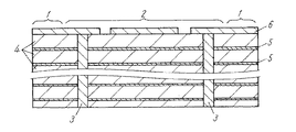
図3は、従来の半導体装置の断面図であり、半導体チップと半導体チップの間のスクライブライン領域を示している。二つの半導体チップ1の間には、スクライブライン領域2があり、半導体チップ1の周辺には、シールリング3が形成されている。半導体チップ1およびスクライブライン領域2には、層間絶縁膜4と、固い層間絶縁膜5がそれぞれ複数層積層され、最上層には保護膜6が形成されている。
FIG. 3 is a cross-sectional view of a conventional semiconductor device, and shows a scribe line region between semiconductor chips. There is a
従来、半導体ウェハーのダイシングにおいて、各配線層の層間絶縁膜4、5は固く、また層数も少なく単純なため、チッピングあるいは剥離等は小さく、問題にはならなかった。しかしながら、スクライブライン領域の縮小化や拡散プロセスの微細化技術の進展に伴い、プロセス・コントロール・モジュレーション(以下、PCMと略す)領域が複雑かつ増大し、スクライブライン領域の有効活用のためにPCMをスクライブライン領域に搭載することがおこなわれるようになり、スクライブライン領域のパターンが複雑になってきた。このことは、半導体の回路形成を担う拡散工程が完了した後の半導体素子のパッケージングを担う組立工程、特にダイシング工程で問題となってくる。具体的には、スクライブライン領域に余裕がなくなり、また、スクライブライン領域へPCM搭載によるパターンの複雑化により、半導体ウェハーをダイシングして、半導体チップ個片にする際に、保護膜あるいは層間絶縁膜にチッピングや剥離、ダメージが起こり、信頼性不良の原因となる。
Conventionally, in the dicing of a semiconductor wafer, since the
そこで、従来は各半導体チップ領域間のスクライブライン領域の最上層の保護膜に保護膜のない溝を形成することにより、半導体チップ領域へのチッピングを防止する半導体装置を形成している(例えば、特許文献1参照)。
しかしながら、さらなる拡散プロセスの微細化に伴い、拡散プロセスにおける平坦化技術が進み、平坦化するための機械的化学研磨により各配線層の層間絶縁膜の薄膜化が進み、これに伴い、工程数及び層間絶縁膜の各層数が増加し複雑になってきた。その上さらに、同じく拡散プロセスの微細化技術により、配線遅延の問題が顕著になってきており、その配線間遅延を小さくするため配線間に挟まれている絶縁膜に誘電率の低い絶縁膜(低誘電率膜)を採用しようとしている。しかし、この低誘電率膜は、従来から採用されていたシリコン酸化膜よりも機械的強度が大きく低下する。そのため、従来のスクライブライン構造では、もはや半導体組立工程であるダイシングの衝撃によるスクライブライン領域の保護膜及び各配線層のチッピングあるいは内部剥離、ダメージを防止することが困難になってきた。 However, along with further miniaturization of the diffusion process, the planarization technique in the diffusion process has progressed, and the thinning of the interlayer insulating film of each wiring layer has progressed by mechanical chemical polishing for planarization. The number of layers of the interlayer insulating film has increased and has become complicated. In addition, the problem of wiring delay has become remarkable due to the same miniaturization technique of the diffusion process. In order to reduce the delay between the wirings, an insulating film having a low dielectric constant ( A low dielectric constant film is being adopted. However, the mechanical strength of this low dielectric constant film is significantly lower than that of a silicon oxide film conventionally employed. Therefore, in the conventional scribe line structure, it has become difficult to prevent chipping or internal peeling and damage of the protective film and each wiring layer in the scribe line region due to the impact of dicing, which is a semiconductor assembly process.
本発明は上記従来の課題を解決するもので、スクライブライン領域の保護膜及び各配線層のチッピング或いは内部剥離、ダメージを防止する半導体装置を提供することを目的とする。 SUMMARY OF THE INVENTION The present invention solves the above-described conventional problems, and an object thereof is to provide a semiconductor device that prevents chipping or internal peeling and damage of a protective film in a scribe line region and each wiring layer.
この課題を解決するために本発明は、拡散プロセスの配線工程によって固い層間絶縁膜と柔らかい層間絶縁膜とが交互に形成され、その固い層間絶縁膜をスクライブライン領域において、すべて除去あるいは一部除去することを特徴とするものである。 In order to solve this problem, according to the present invention, a hard interlayer insulating film and a soft interlayer insulating film are alternately formed by a wiring process of a diffusion process, and the hard interlayer insulating film is completely or partially removed in the scribe line region. It is characterized by doing.
従来は、スクライブライン領域にもチップ側と同様に固い層間絶縁膜と柔らかい層間絶縁膜とが交互に形成されているが、本発明の半導体装置では、そのスクライブライン領域の固い層間絶縁膜を全て除去することによって、ダイシングの際に、固い層間絶縁膜を切断することなく、柔らかい層間絶縁膜のみを切断するため、スクライブライン領域の保護膜及び各配線層の層間絶縁膜のチッピングあるいは内部剥離、ダメージの防止を実現できる。また、スクライブライン領域において、PCM等固い層間絶縁膜が必要な部分は残して、シールリングのスクライブライン側に固い層間絶縁膜を溝のように1部除去する場合は、ダイシングの際に、固い層間絶縁膜を切断することになるが、固い層間絶縁膜がチップ側で除去されているため、ダイシング時の衝撃はチップ側へ影響しない。従って、スクライブライン領域の固い層間絶縁膜を全て除去した場合と同様の効果があり、スクライブライン領域の保護膜及び各配線層の層間絶縁膜のチッピングあるいは内部剥離、ダメージの防止を実現できる。 Conventionally, a hard interlayer insulating film and a soft interlayer insulating film are alternately formed in the scribe line region as well as on the chip side. However, in the semiconductor device of the present invention, all the hard interlayer insulating films in the scribe line region are formed. By removing, in order to cut only the soft interlayer insulating film without cutting the hard interlayer insulating film at the time of dicing, chipping or internal peeling of the protective film of the scribe line region and the interlayer insulating film of each wiring layer, Damage prevention can be realized. Also, in the scribe line region, when a part of the hard interlayer insulating film such as a groove is removed on the scribe line side of the seal ring while leaving a portion where a hard interlayer insulating film such as PCM is required, it is hard to dice during dicing. Although the interlayer insulating film is cut, since the hard interlayer insulating film is removed on the chip side, the impact during dicing does not affect the chip side. Therefore, the same effect as when all the hard interlayer insulating films in the scribe line region are removed can be achieved, and chipping or internal peeling and damage prevention of the protective film in the scribe line region and the interlayer insulating film in each wiring layer can be realized.
以上のように、スクライブライン領域において、固い層間絶縁膜をすべて除去あるいは1部除去することにより、半導体ウェハーのダイシング時の衝撃に対し、チッピング及び内部剥離、ダメージを防止することができる。その結果、半導体の信頼性を向上することが可能となる。 As described above, by removing all or one part of the hard interlayer insulating film in the scribe line region, it is possible to prevent chipping, internal peeling, and damage against the impact during dicing of the semiconductor wafer. As a result, it is possible to improve the reliability of the semiconductor.
以下、本発明の半導体装置の実施形態について図面に基づき詳細に説明する。 DESCRIPTION OF EMBODIMENTS Hereinafter, embodiments of a semiconductor device of the present invention will be described in detail with reference to the drawings.
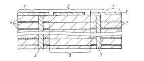
図1は、本発明の第1の実施形態における半導体装置の断面図であり、半導体チップと半導体チップの間のスクライブライン領域を示している。半導体ウェハー上に形成されたそれぞれの半導体チップ1の間には、スクライブライン領域2があり、半導体チップ1の周辺には、シールリング3が形成されている。半導体チップ1の領域では、柔らかい層間絶縁膜4と、固い層間絶縁膜7がそれぞれ複数層積層され、最上層には保護膜6が形成されている。シールリング3のスクライブ側、つまりスクライブライン領域2におけるチッピング及び内部剥離防止部8では、柔らかい層間絶縁膜4のみが複数層積層され、最上層には保護膜6が形成されている。各層間絶縁膜4の間には固い層間絶縁膜7を形成しない。
FIG. 1 is a cross-sectional view of a semiconductor device according to a first embodiment of the present invention, and shows a scribe line region between semiconductor chips. There is a
図1に示すように固い層間絶縁膜7の除去されている部分であるチッピング及び内部剥離防止部8でダイシングのブレードにより半導体ウェハーが切断され、各半導体チップに分離される。従って、固い層間絶縁膜を切断することなく、柔らかい層間絶縁膜4のみを切断することになり、チッピング及び切断面の内部剥離やダメージを防止することができる。固い層間絶縁膜7としては、SiN膜やSiC膜などがあげられる。
As shown in FIG. 1, a semiconductor wafer is cut by a dicing blade at a chipping and internal
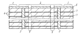
次に、図2は本発明の第2の実施形態における半導体装置の断面図であり、半導体チップと半導体チップの間のスクライブライン領域を示している。図1の第1の実施形態と異なる点は、シールリング3のスクライブ側、つまりスクライブライン領域2の一部にチッピング及び内部剥離防止部9を設け、チッピング及び内部剥離防止部9だけは、柔らかい層間絶縁膜4のみが複数層積層されており、各層間絶縁膜4の間には固い層間絶縁膜7を形成しない。それぞれのチッピング及び内部剥離防止部9を除く内側のスクライブライン領域2には、半導体チップ1の領域と同様に柔らかい層間絶縁膜4と、固い層間絶縁膜7がそれぞれ複数層積層され、最上層には保護膜6が形成されている。つまり、スクライブライン領域2においては、半導体チップ1側の一定距離以内の領域、シールリング3のスクライブ側の一部であるチッピング及び内部剥離防止部9の領域のみ、固い層間絶縁膜7が両側溝のように除去されている。
Next, FIG. 2 is a cross-sectional view of the semiconductor device according to the second embodiment of the present invention, and shows a scribe line region between the semiconductor chips. 1 differs from the first embodiment of FIG. 1 in that a chipping and internal peeling prevention portion 9 is provided on the scribe side of the
図2に示す半導体装置のダイシングでは、スクライブライン領域2の中間部でダイシングのブレードにより半導体ウェハーが切断され、各半導体チップに分離される。従って、固い層間絶縁膜7を切断することになるが、両側に柔らかい層間絶縁膜4のみの部分、つまりチッピング及び内部剥離防止部9があるために、応力が吸収され、チッピング及び切断面の内部剥離やダメージを防止することができる。
In the dicing of the semiconductor device shown in FIG. 2, the semiconductor wafer is cut by a dicing blade at an intermediate portion of the
本発明の半導体装置におけるスクライブライン領域の構成は、固い膜と柔らかい膜が積層されているものを細片化する際の切断に有効であり、Si半導体、化合物半導体や半導体以外の電子部品にも同様の構成の場合に利用可能である。 The structure of the scribe line region in the semiconductor device of the present invention is effective for cutting when a hard film and a soft film are laminated, and is also used for electronic parts other than Si semiconductors, compound semiconductors, and semiconductors. It can be used in the case of a similar configuration.
1 半導体チップ
2 スクライブライン領域
3 シールリング
4 層間絶縁膜
6 保護膜
7 層間絶縁膜
8 チッピング及び内部剥離防止部
DESCRIPTION OF SYMBOLS 1
Claims (3)
Priority Applications (1)
| Application Number | Priority Date | Filing Date | Title |
|---|---|---|---|
| JP2004109794A JP2005294677A (en) | 2004-04-02 | 2004-04-02 | Semiconductor device |
Applications Claiming Priority (1)
| Application Number | Priority Date | Filing Date | Title |
|---|---|---|---|
| JP2004109794A JP2005294677A (en) | 2004-04-02 | 2004-04-02 | Semiconductor device |
Publications (1)
| Publication Number | Publication Date |
|---|---|
| JP2005294677A true JP2005294677A (en) | 2005-10-20 |
Family
ID=35327245
Family Applications (1)
| Application Number | Title | Priority Date | Filing Date |
|---|---|---|---|
| JP2004109794A Withdrawn JP2005294677A (en) | 2004-04-02 | 2004-04-02 | Semiconductor device |
Country Status (1)
| Country | Link |
|---|---|
| JP (1) | JP2005294677A (en) |
Cited By (3)
| Publication number | Priority date | Publication date | Assignee | Title |
|---|---|---|---|---|
| JP2020031204A (en) * | 2018-08-17 | 2020-02-27 | キオクシア株式会社 | Semiconductor substrate and semiconductor device |
| US10930602B2 (en) | 2018-10-19 | 2021-02-23 | Samsung Electronics Co., Ltd. | Semiconductor device and method for fabricating the same |
| CN114446876A (en) * | 2022-04-12 | 2022-05-06 | 湖北三维半导体集成创新中心有限责任公司 | Wafer cutting method |
-
2004
- 2004-04-02 JP JP2004109794A patent/JP2005294677A/en not_active Withdrawn
Cited By (6)
| Publication number | Priority date | Publication date | Assignee | Title |
|---|---|---|---|---|
| JP2020031204A (en) * | 2018-08-17 | 2020-02-27 | キオクシア株式会社 | Semiconductor substrate and semiconductor device |
| JP7288300B2 (en) | 2018-08-17 | 2023-06-07 | キオクシア株式会社 | Semiconductor substrate and semiconductor device |
| US10930602B2 (en) | 2018-10-19 | 2021-02-23 | Samsung Electronics Co., Ltd. | Semiconductor device and method for fabricating the same |
| US11784137B2 (en) | 2018-10-19 | 2023-10-10 | Samsung Electronics Co., Ltd. | Semiconductor device and method for fabricating the same |
| CN114446876A (en) * | 2022-04-12 | 2022-05-06 | 湖北三维半导体集成创新中心有限责任公司 | Wafer cutting method |
| CN114446876B (en) * | 2022-04-12 | 2022-07-01 | 湖北三维半导体集成创新中心有限责任公司 | Wafer cutting method |
Similar Documents
| Publication | Publication Date | Title |
|---|---|---|
| JP5448304B2 (en) | Semiconductor device | |
| US7417304B2 (en) | Electronic device and method for fabricating the same | |
| CN100385627C (en) | Manufacturing method of semiconductor device, semiconductor wafer and semiconductor device | |
| JP5175066B2 (en) | Semiconductor device | |
| JP5235378B2 (en) | Semiconductor device | |
| CN102593076B (en) | Semiconductor device | |
| JP2010074106A (en) | Semiconductor chip, semiconductor wafer, and method of dicing the same | |
| US20050093169A1 (en) | Semiconductor device and method of manufacturing semiconductor device | |
| CN102842597B (en) | Semiconductor chip and semiconductor device | |
| JP2011139103A (en) | Semiconductor device | |
| JP4383274B2 (en) | Semiconductor device and semiconductor wafer manufacturing method | |
| US20090224387A1 (en) | Semiconductor chip and method for manufacturing the same and semiconductor device | |
| US7777304B2 (en) | Semiconductor device | |
| US9437556B2 (en) | Semiconductor device | |
| JP2009218504A (en) | Semiconductor device | |
| CN100463190C (en) | SOI substrate and its manufacturing method | |
| JP2005294677A (en) | Semiconductor device | |
| JP2012160547A (en) | Semiconductor device and manufacturing method of the same | |
| JP2009076782A (en) | Semiconductor substrate, manufacturing method thereof, and semiconductor chip | |
| JP5726989B2 (en) | Semiconductor device | |
| JP2008041804A (en) | Semiconductor device and manufacturing method thereof | |
| JP2006147626A (en) | Semiconductor device | |
| JP4814694B2 (en) | Semiconductor device | |
| JP2009218503A (en) | Semiconductor device and manufacturing method thereof | |
| JP2006269837A (en) | Semiconductor element assembly, semiconductor element manufacturing method, and semiconductor element |
Legal Events
| Date | Code | Title | Description |
|---|---|---|---|
| A621 | Written request for application examination |
Free format text: JAPANESE INTERMEDIATE CODE: A621 Effective date: 20070219 |
|
| RD01 | Notification of change of attorney |
Free format text: JAPANESE INTERMEDIATE CODE: A7421 Effective date: 20070313 |
|
| A761 | Written withdrawal of application |
Free format text: JAPANESE INTERMEDIATE CODE: A761 Effective date: 20070730 |