JP2005294484A - Semiconductor light emitting device and manufacturing method - Google Patents
Semiconductor light emitting device and manufacturing method Download PDFInfo
- Publication number
- JP2005294484A JP2005294484A JP2004106643A JP2004106643A JP2005294484A JP 2005294484 A JP2005294484 A JP 2005294484A JP 2004106643 A JP2004106643 A JP 2004106643A JP 2004106643 A JP2004106643 A JP 2004106643A JP 2005294484 A JP2005294484 A JP 2005294484A
- Authority
- JP
- Japan
- Prior art keywords
- light emitting
- cavity
- semiconductor light
- phosphor
- emitting element
- Prior art date
- Legal status (The legal status is an assumption and is not a legal conclusion. Google has not performed a legal analysis and makes no representation as to the accuracy of the status listed.)
- Granted
Links
Images


Classifications
-
- H—ELECTRICITY
- H10—SEMICONDUCTOR DEVICES; ELECTRIC SOLID-STATE DEVICES NOT OTHERWISE PROVIDED FOR
- H10H—INORGANIC LIGHT-EMITTING SEMICONDUCTOR DEVICES HAVING POTENTIAL BARRIERS
- H10H20/00—Individual inorganic light-emitting semiconductor devices having potential barriers, e.g. light-emitting diodes [LED]
- H10H20/80—Constructional details
- H10H20/85—Packages
- H10H20/851—Wavelength conversion means
- H10H20/8516—Wavelength conversion means having a non-uniform spatial arrangement or non-uniform concentration, e.g. patterned wavelength conversion layer or wavelength conversion layer with a concentration gradient
-
- H—ELECTRICITY
- H10—SEMICONDUCTOR DEVICES; ELECTRIC SOLID-STATE DEVICES NOT OTHERWISE PROVIDED FOR
- H10W—GENERIC PACKAGES, INTERCONNECTIONS, CONNECTORS OR OTHER CONSTRUCTIONAL DETAILS OF DEVICES COVERED BY CLASS H10
- H10W74/00—Encapsulations, e.g. protective coatings
Landscapes
- Led Device Packages (AREA)
- Led Devices (AREA)
Abstract
【課題】本発明は、色ムラ及び輝度バラツキが少なく、人間に対して有害となる可能性のある光を極力放出しない光源となるような半導体発光装置及び製造方法を提供する。
【解決手段】反射面2が形成された傾斜面を有する第一のキャビティ22の上方に略垂直な内周面を有する第二のキャビティ24を設けた。そして、底部に半導体発光素子4を搭載した第一のキャビティ22内及び第二のキャビティ24内に透光性樹脂に蛍光体を分散した蛍光体分散樹脂6を第二のキャビティ24の上面に対して凸形状に盛り上げて充填し、そのまま反転して蛍光体分散樹脂6を加熱硬化させるときに、透光性樹脂より比重が大きい蛍光体5が沈降して蛍光体分散樹脂6の表面付近に高密度蛍光体層8が形成される。
【選択図】 図3The present invention provides a semiconductor light emitting device and a manufacturing method that can be a light source that emits as little light as possible with less color unevenness and luminance variation and may be harmful to humans.
A second cavity having a substantially vertical inner peripheral surface is provided above a first cavity having an inclined surface on which a reflecting surface is formed. Then, the phosphor dispersion resin 6 in which the phosphor is dispersed in the translucent resin in the first cavity 22 and the second cavity 24 in which the semiconductor light emitting element 4 is mounted on the bottom is formed on the upper surface of the second cavity 24. When the phosphor-dispersed resin 6 is heated and cured by inversion, the phosphor 5 having a specific gravity larger than that of the translucent resin is settled and becomes high near the surface of the phosphor-dispersed resin 6. A density phosphor layer 8 is formed.
[Selection] Figure 3
Description
本発明は、半導体発光装置及び製造方法に関するものであり、詳しくは半導体発光素子から発せられた光と、半導体発光素子から発せられて蛍光体によって波長変換された光との組み合わせの加法混色によって任意の発光色の光を発する半導体発光装置及び製造方法に関する。 The present invention relates to a semiconductor light emitting device and a manufacturing method, and in particular, can be arbitrarily determined by additive color mixing of a combination of light emitted from a semiconductor light emitting element and light emitted from the semiconductor light emitting element and wavelength-converted by a phosphor. The present invention relates to a semiconductor light emitting device that emits light of the emission color and a manufacturing method thereof.
急峻なスペクトル分布を有した光を発する発光ダイオード(LED)チップを光源にして白色光を放出するLEDを実現するためには、LEDチップから発せられた光と、LEDチップから発せられた光によって励起された蛍光体が発する波長変換された光との加法混色によって可能になる。 In order to realize an LED that emits white light by using a light emitting diode (LED) chip that emits light having a steep spectral distribution as a light source, the light emitted from the LED chip and the light emitted from the LED chip are used. This is made possible by additive color mixing with the wavelength-converted light emitted by the excited phosphor.
例えば、LEDチップから発せられる光が青色光の場合は、青色光に励起されて青色の補色となる黄色の光に波長変換する蛍光体を使用することにより、LEDチップから発せられた青色光と、LEDチップから発せられた青色光によって励起された蛍光体が発する波長変換された黄色光との加法混色によって白色光を得ることができる。 For example, when the light emitted from the LED chip is blue light, by using a phosphor that converts the wavelength into yellow light that is excited by the blue light and becomes a complementary color of blue, the blue light emitted from the LED chip White light can be obtained by additive color mixture with wavelength-converted yellow light emitted from a phosphor excited by blue light emitted from an LED chip.
同様に、LEDチップから発せられる光が青色光の場合、青色光に励起されて夫々緑色光及び赤色光に波長変換する2種類の蛍光体を混合して使用することにより、LEDチップから発せられた青色光と、LEDチップから発せられた青色光によって励起された2種類の蛍光体が発する波長変換された緑色光及び赤色光との加法混色によって白色光を得ることができる。 Similarly, when the light emitted from the LED chip is blue light, it is emitted from the LED chip by using a mixture of two types of phosphors that are excited by blue light and wavelength-converted into green light and red light, respectively. White light can be obtained by additive color mixing of the blue light and the wavelength-converted green light and red light emitted by the two types of phosphors excited by the blue light emitted from the LED chip.
また、LEDチップから発せられる光が紫外線の場合、紫外線に励起されて夫々青色光、緑色光及び赤色光に波長変換する3種類の蛍光体を混合して使用することにより、LEDチップから発せられた紫外線によって励起された3種類の蛍光体が発する波長変換された青色光、緑色光及び赤色光との加法混色によって白色光を得ることができる。 In addition, when the light emitted from the LED chip is ultraviolet light, it is emitted from the LED chip by using a mixture of three kinds of phosphors that are excited by the ultraviolet light and convert the wavelengths into blue light, green light, and red light, respectively. White light can be obtained by additive color mixture of wavelength-converted blue light, green light, and red light emitted by three types of phosphors excited by ultraviolet light.
さらに、LEDチップから発せられる光の発光色と波長変換部材となる蛍光体とを適宜組み合わせることによって白色光以外の種々な色調の光を得ることができる。 Furthermore, light of various color tones other than white light can be obtained by appropriately combining the emission color of the light emitted from the LED chip and the phosphor as the wavelength conversion member.
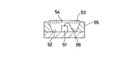
上記のように、光源から発せられた光で蛍光体を励起して波長変換し、光源から発せられた光とは異なる色調の光を放出するようなLEDには、例えば図4に示すようなものがある。これは、底部に発光素子51を配置してボンディングワイヤ56で電気的導通を図ったカップ52の中に波長変換部材となる蛍光体53を分散した樹脂54を充填し、これをケース55の天面に蓋をして上下を反転させた状態で樹脂54の加熱硬化を行うことにより樹脂よりも比重が大きい蛍光体53が沈んでカップ52の上部に溜まる。その結果、カップ52の下部よりも上部の方が蛍光体53の密度が高い分布のLEDを実現したものである(例えば、特許文献1参照。)。
As described above, for an LED that excites a phosphor with light emitted from a light source, converts the wavelength, and emits light having a color tone different from that of the light emitted from the light source, for example, as shown in FIG. There is something. In this case, a
また、図5に示すように、底部にLEDチップ61を配置してボンディングワイヤ62で電気的導通を図ったカップ63の中に第一の光透過性樹脂64をカップ容積の60%ないし70%程度充填して加熱硬化する。そして更にその上に光透過性樹脂に波長変換部材となる蛍光体65を分散した第二の光透過性樹脂66をカップ容積の50%ないし60%程度注入し、これを上下を反転させた状態で加熱硬化を行うことにより第二の光透過性樹脂66はカップ63の外縁に沿って凸状に膨らみ、第二の光透過性樹脂66に分散された蛍光体65が沈んで凸状に膨らんだ上部に溜まる。その結果、蛍光体65が凸レンズ状の表面付近に高密度に分布するようなLEDを実現したものである(例えば、特許文献2参照。)。
上述したような従来のLEDにおいて、前者は、ケースの天面に蓋をして上下を反転させた状態でカップ内に充填された樹脂の加熱硬化を行う際に、ケ−スの天面と蓋とは全面に亘って隙間なく密着していることが必要であり、少しでも隙間が存在すればその隙間を介してカップ内から樹脂が漏れ出して不良品を発生させることになる。 In the conventional LED as described above, when the former is covered with the top of the case and the resin filled in the cup is turned upside down, the top of the case is It is necessary that the lid is in close contact with the entire surface without any gap, and if any gap exists, the resin leaks from the cup through the gap and a defective product is generated.
特に、大型のケースに多数のカップを形成して一括大量生産を行う場合、カップ天面と蓋とが全面に亘って密着するような極めて高い面精度を確保することは非常に難しく、可能であるとしてもコストが高額なものになることは明らかである。その上、樹脂の加熱硬化時の熱によって密着面を形成するケース及び蓋の夫々に生じる膨張や反り等の変形が益々両部材の密着性を阻害することになり、製造歩留まりの悪化は避けられないものとなる。 In particular, when mass production is performed by forming a large number of cups in a large case, it is very difficult and possible to ensure extremely high surface accuracy such that the cup top surface and the lid are in close contact with each other. Obviously, the cost will be high if any. In addition, deformations such as expansion and warpage that occur in the case and lid that form the adhesion surface due to heat at the time of heat curing of the resin will further impede the adhesion between the two members, and deterioration in manufacturing yield can be avoided. It will not be.
更に、発光光量を増すために発光素子を大型化して大電流を流すことが行われるが、それに対してパッケージの大きさに実用上の限度がある。従って、発光素子を配置するカップの大きさも限定されることになり、カップの内容積に対して発光素子の占める割合が従来の同じタイプのLEDよりも大きくなる。言い換えると、カップの内容積に対してカップの内容積から発光素子の体積を差し引いたカップの空間容積の比率が減少することになる。 Furthermore, in order to increase the amount of emitted light, the light emitting element is enlarged and a large current is passed, but there is a practical limit on the size of the package. Therefore, the size of the cup in which the light emitting element is arranged is also limited, and the ratio of the light emitting element to the inner volume of the cup is larger than that of the conventional LED of the same type. In other words, the ratio of the space volume of the cup obtained by subtracting the volume of the light emitting element from the volume of the cup with respect to the volume of the cup decreases.
すると、発光素子の側面とカップの内周面との距離及び発光素子の上面とカップに充填された蛍光体が分散された樹脂の天面との距離が近接した状態になる。このとき、発光素子の上面と樹脂の天面との間に存在する樹脂の量よりも発光素子の側面とカップの内周面との間に存在する樹脂の量の方が多い。これは、樹脂の中に分散された蛍光体の量についても同様のことが言える。 Then, the distance between the side surface of the light emitting element and the inner peripheral surface of the cup and the distance between the upper surface of the light emitting element and the top surface of the resin in which the phosphor filled in the cup is dispersed are close to each other. At this time, the amount of the resin existing between the side surface of the light emitting element and the inner peripheral surface of the cup is larger than the amount of resin existing between the upper surface of the light emitting element and the top surface of the resin. The same can be said for the amount of phosphor dispersed in the resin.
このような状態のケースの天面に蓋をして上下反転させて樹脂の加熱硬化を行ことにより、樹脂よりも比重が大きい蛍光体が沈んでカップの上部に溜まり、カップの下部よりも上部の方が蛍光体の密度が高い分布のLEDを実現できる。但し、上記のように発光素子の上面と樹脂の天面との間に存在する樹脂中の蛍光体の量よりも発光素子の側面とカップの内周面との間に存在する樹脂中の蛍光体の量の方が多いために、上下反転して樹脂を加熱硬化するときには発光素子上部の蛍光体の沈殿量に対してその周囲の沈殿量が多くなり、蛍光体の層を均一に形成することが困難なものとなる。 By covering the top surface of the case in this state and turning it upside down and curing the resin by heating, the phosphor with a higher specific gravity than the resin sinks and accumulates at the top of the cup, and above the bottom of the cup. It is possible to realize LEDs having a distribution in which the phosphor density is higher. However, as described above, the fluorescence in the resin existing between the side surface of the light emitting element and the inner peripheral surface of the cup is larger than the amount of the phosphor in the resin existing between the upper surface of the light emitting element and the top surface of the resin. Since the amount of the body is larger, when the resin is turned upside down and the resin is heat-cured, the amount of the surrounding precipitate is larger than the amount of the phosphor deposited on the top of the light emitting element, and the phosphor layer is uniformly formed. It becomes difficult.
その結果、発光素子から発せられて高密度の蛍光体の層に至った光が場所によって蛍光体を励起する確立が異なるために、色ムラのある光源となる問題点を有している。特に、白色光を放出するLEDについては色ムラは実用上厳格に規定され、歩留まりが悪くなる可能性が極めて高くなる。 As a result, since the light emitted from the light-emitting element and reaching the high-density phosphor layer excites the phosphor depending on the location, there is a problem that the light source has uneven color. In particular, for an LED that emits white light, the color unevenness is strictly defined for practical use, and the possibility that the yield deteriorates becomes extremely high.
一方後者は、第一の光透過性樹脂が表面張力によってカップの外縁まで這い上がり、この状態で更にその上に蛍光体を分散した第二の光透過性樹脂で凸レンズ状を形成して凸レンズ状の膨らみ部分の表面付近に高密度の蛍光体の層を設けるものであるが、第二の光透過性樹脂の膨らみ部分に対して端部には蛍光体の量が少なく、同時に第一の光透過性樹脂の這い上がり部分には第二の透過性樹脂が行き届かず蛍光体層が形成されない可能性が生じる。 On the other hand, in the latter case, the first light-transmitting resin crawls up to the outer edge of the cup due to surface tension, and in this state, a convex lens shape is formed by forming the second light-transmitting resin on which the phosphor is further dispersed. A high-density phosphor layer is provided in the vicinity of the surface of the bulging portion of the second light-transmitting resin. There is a possibility that the second transparent resin does not reach the rising portion of the transparent resin and the phosphor layer is not formed.
本来、発光素子から発せられた光と、発光素子から発せられて蛍光体の層で波長変換された光との加法混色によって略全方向に亘って色ムラの少ない白色光を発するようにLEDが構成されるべきものであるが、発光素子から発せられて蛍光体の層を通らないで直接LEDから放出される光が一定の範囲内に存在すると、その部分では加法混色の光ではなく発光素子から発せられた光のみがそのまま放出されることになる。 Originally, an LED emits white light with little color unevenness in almost all directions by additive color mixing of light emitted from a light emitting element and light emitted from the light emitting element and converted in wavelength by a phosphor layer. Although light that is emitted from the light emitting element and directly emitted from the LED without passing through the phosphor layer is within a certain range, the light emitting element is not an additive color mixture light in that portion. Only the light emitted from is emitted as it is.
その場合、発光素子の発する光のピーク発光波長が約450nm〜470nmの青色光の場合、発光素子から発せられて蛍光体の層が形成された範囲内を導光されてLEDから放出される光は白色光(W)であり、発光素子から発せられて蛍光体の層が形成されていない部分を導光されて直接LEDから放出される光は青色光(B)であり、白色LEDとしては白色と青色の色ムラのある光を発することになり、良好な製品とはならない。 In that case, in the case of blue light having a peak emission wavelength of about 450 nm to 470 nm of light emitted from the light emitting element, light emitted from the LED after being guided from within the range where the phosphor layer is formed. Is white light (W), and the light emitted from the light emitting element and guided through the portion where the phosphor layer is not formed and directly emitted from the LED is blue light (B). It will emit light with white and blue color unevenness, and it will not be a good product.
また、発光素子の発する光のピーク発光波長が約400nm以下の短波長領域の場合、このような紫外線がLEDから直接放出されて直接人間の目に入ることになると何らかの悪影響を及ぼす恐れがあり、好ましいものではない。 Further, in the case of a short wavelength region where the peak emission wavelength of light emitted from the light emitting element is about 400 nm or less, there is a possibility that such ultraviolet rays may be directly emitted from the LED and directly enter the human eye, and have some adverse effects. It is not preferable.
そこで、本発明は上記問題に鑑みて創案なされたもので、色ムラ及び輝度バラツキが少なく、人間に対して有害となる可能性のある光を極力放出しない光源となるような半導体発光装置及び製造方法を提供する。 Accordingly, the present invention was devised in view of the above problems, and a semiconductor light emitting device and a manufacturing method that can be a light source that emits as little light as possible with little color unevenness and luminance variation and may be harmful to humans. Provide a method.
上記課題を解決するために、本発明の請求項1に記載された発明は、ケースに設けられた開口部を有する凹形状のキャビティの底部に少なくとも1つの半導体発光素子が搭載され、前記キャビティ内に該キャビティの表面に対して前記半導体発光素子の略放射方向に凸形状に盛り上げて充填された樹脂の表面付近全面に亘って高密度の波長変換部材の層が形成されていることを特徴とするものである。 In order to solve the above-described problems, according to a first aspect of the present invention, at least one semiconductor light emitting element is mounted on the bottom of a concave cavity having an opening provided in a case, Further, a high-density wavelength conversion member layer is formed over the entire surface near the surface of the resin that is raised and filled in a substantially radial direction of the semiconductor light emitting element with respect to the surface of the cavity. To do.
また、本発明の請求項2に記載された発明は、請求項1において、前記キャビティは、該キャビティの底部に搭載された前記半導体発光素子の光軸に対して前記半導体発光素子の略放射方向に向かって開いた直線を前記光軸を中心として回転した傾斜曲面を有し、該傾斜曲面が反射面であることを特徴とするものである。 According to a second aspect of the present invention, in the first aspect, the cavity has a substantially radial direction of the semiconductor light emitting element with respect to an optical axis of the semiconductor light emitting element mounted on the bottom of the cavity. And a slanted curved surface obtained by rotating a straight line opened toward the center about the optical axis, and the slanted curved surface is a reflecting surface.
また、本発明の請求項3に記載された発明は、請求項1において、前記キャビティは、底部に搭載された半導体発光素子の光軸に対して前記半導体発光素子の略放射方向に向かって開いた直線を前記光軸を中心として回転した傾斜曲面を有する第一のキャビティと、該第一のキャビティの上方にあって前記半導体発光素子の光軸に対して略平行な直線を前記光軸を中心として回転した垂直曲面を有する第二のキャビティとからなり、前記第一のキャビティの傾斜曲面と前記第二のキャビティの垂直曲面のうちの何れか一方または両方が反射面であることを特徴とするものである。 According to a third aspect of the present invention, in the first aspect, the cavity opens in a substantially radial direction of the semiconductor light emitting element with respect to the optical axis of the semiconductor light emitting element mounted on the bottom. A first cavity having an inclined curved surface rotated about the optical axis, and a straight line above the first cavity and substantially parallel to the optical axis of the semiconductor light emitting element. A second cavity having a vertical curved surface rotated as a center, and one or both of the inclined curved surface of the first cavity and the vertical curved surface of the second cavity are reflection surfaces, To do.
また、本発明の請求項4に記載された発明は、開口部を有する凹形状のキャビティが形成されたケースを準備する工程と、
前記キャビティの底部に少なくとも1つの半導体発光素子を搭載する工程と、
前記キャビティ内に波長変換部材を分散した透光性樹脂を充填する工程と、
前記キャビティ内に前記波長変換部材を分散した透光性樹脂が充填されたケースを反転して前記波長変換部材を分散した透光性樹脂を硬化する工程と、
を有することを特徴とするものである。
Moreover, the invention described in claim 4 of the present invention includes a step of preparing a case in which a concave cavity having an opening is formed,
Mounting at least one semiconductor light emitting device on the bottom of the cavity;
Filling a translucent resin in which a wavelength conversion member is dispersed in the cavity;
Reversing the case filled with the translucent resin in which the wavelength conversion member is dispersed in the cavity and curing the translucent resin in which the wavelength conversion member is dispersed;
It is characterized by having.
また、本発明の請求項5に記載された発明は、請求項4において、前記波長変換部材を分散した透光性樹脂を硬化する工程において、前記波長変換部材を分散した透光性樹脂は前記キャビティ内に前記キャビティの表面に対して前記半導体発光素子の放射方向に凸形状に盛り上げて充填されて表面付近全面に亘って高密度の波長変換部材の層が形成されることを特徴とするものである。
Further, in the invention described in
また、本発明の請求項6に記載された発明は、請求項4または5の何れか1項において、前記キャビティは、該キャビティの底部に搭載された前記半導体発光素子の光軸に対して前記半導体発光素子の略放射方向に向かって開いた直線を前記光軸を中心として回転した傾斜曲面を有し、該傾斜曲面が反射面であることを特徴とするものである。 According to a sixth aspect of the present invention, in any one of the fourth or fifth aspect, the cavity is arranged with respect to an optical axis of the semiconductor light emitting device mounted on the bottom of the cavity. The semiconductor light emitting device has an inclined curved surface obtained by rotating a straight line opened substantially in the radiation direction about the optical axis, and the inclined curved surface is a reflecting surface.
また、本発明の請求項7に記載された発明は、請求項4または5の何れか1項において、前記キャビティは、底部に搭載された半導体発光素子の光軸に対して前記半導体発光素子の略放射方向に向かって開いた直線を前記光軸を中心として回転した傾斜曲面を有する第一のキャビティと、該第一のキャビティの上方にあって前記半導体発光素子の光軸に対して略平行な直線を前記光軸を中心として回転した垂直曲面を有する第二のキャビティとからなり、前記第一のキャビティの傾斜曲面と前記第二のキャビティの垂直曲面のうちの何れか一方または両方が反射面であることを特徴とするものである。 According to a seventh aspect of the present invention, in any one of the fourth or fifth aspect, the cavity is formed on the semiconductor light emitting element with respect to the optical axis of the semiconductor light emitting element mounted on the bottom. A first cavity having an inclined curved surface rotated about the optical axis as a straight line opened substantially in the radial direction, and substantially parallel to the optical axis of the semiconductor light emitting element above the first cavity. And a second cavity having a vertical curved surface rotated about the optical axis, and one or both of the inclined curved surface of the first cavity and the vertical curved surface of the second cavity are reflected. It is a surface.
色ムラ及び輝度バラツキが少なく、人間に対して有害となる可能性のある光を極力放出しない半導体発光装置を実現する目的を、半導体発光素子を波長変換部材を分散した透光性樹脂で凸形状に盛り上げて封止し、表面付近全面に亘って高密度の波長変換部材の層を略均一な密度で且つ略均一な厚みに形成することによって実現した。 For the purpose of realizing a semiconductor light-emitting device that emits as little light as possible with little color unevenness and brightness variation and is harmful to humans, the semiconductor light-emitting element is convex with a translucent resin in which wavelength conversion members are dispersed This was realized by forming a layer of a high-density wavelength conversion member with a substantially uniform density and a substantially uniform thickness over the entire surface.
以下、この発明の好適な実施形態を図1から図3を参照しながら、詳細に説明する(同一部分については同じ符号を付す)。尚、以下に述べる実施形態は、本発明の好適な具体例であるから、技術的に好ましい種々の限定が付されているが、本発明の範囲は、以下の説明において特に本発明を限定する旨の記載がない限り、これらの実施形態に限られるものではない。 Hereinafter, preferred embodiments of the present invention will be described in detail with reference to FIG. 1 to FIG. 3 (the same parts are given the same reference numerals). The embodiments described below are preferable specific examples of the present invention, and thus various technically preferable limitations are given. However, the scope of the present invention particularly limits the present invention in the following description. Unless stated to the effect, the present invention is not limited to these embodiments.
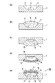
図1(a)〜(e)は本発明の半導体発光装置の製造方法の実施例1を示す工程図である。まず、(a)に示すように高反射率の非透光性樹脂からなるケース1に内周面を反射面2とする擂鉢形状のキャビティ3が設けられ、キャビティ3の底部に半導体発光素子4が配置されている。
1A to 1E are process diagrams showing Example 1 of a method for manufacturing a semiconductor light emitting device of the present invention. First, as shown in (a), a
なお、半導体発光素子4を発光させるためには、半導体発光素子4のアノード電極とカソード電極との間に順方向電圧を印加することが必要であり、そのために半導体発光素子4のアノード電極及びカソード電極の夫々と外部に導出されて電源に接続される端子電極との間に電気的導通を図るための接続手段が施されているが、本実施例を示す図1においてはこれを省略する。 In order to cause the semiconductor light emitting element 4 to emit light, it is necessary to apply a forward voltage between the anode electrode and the cathode electrode of the semiconductor light emitting element 4. For this purpose, the anode electrode and the cathode of the semiconductor light emitting element 4 are required. Connection means for providing electrical continuity is provided between each of the electrodes and a terminal electrode that is led to the outside and connected to the power supply, but this is omitted in FIG. 1 showing the present embodiment.
次に(b)に示すように、キャビティ3内にキャビティ3の上面に対して凸形状に盛り上がった状態になるまで透光性樹脂に波長変換部材となる蛍光体5を分散した蛍光体分散樹脂6を充填する。なお、蛍光体分散樹脂6をキャビティ3の上面に対して盛り上げる度合は、蛍光体分散樹脂6とキャビティ3の上面内縁部7との間の付着力及び蛍光体分散樹脂6の適度な粘性による表面張力によって蛍光体分散樹脂6がキャビティ3内から漏れ出さない範囲内で必要に応じて設定される。
Next, as shown in (b), a phosphor-dispersed resin in which a
次に(c)に示すように、ケース1を反転させてキャビティ3内に充填した蛍光体分散樹脂6を加熱硬化させる。なお、蛍光体分散樹脂6とキャビティ3の上面内縁部7との間の付着力及び蛍光体分散樹脂6の適度な粘性による表面張力がケース1を反転させたときに蛍光体分散樹脂6に作用する重力に対抗する作用となって蛍光体分散樹脂6がキャビティ3から漏れるのを阻止する。従って、蛍光体分散樹脂6の漏れ防止用の蓋は不要である。
Next, as shown in (c), the
ケース1を反転した状態でキャビティ3内に充填した蛍光体分散樹脂6が硬化する過程において(d)に示すように、蛍光体分散樹脂6を構成する透光性樹脂と蛍光体5との比重差によって透光性樹脂よりも比重が大きい蛍光体5が沈降して蛍光体分散樹脂6の表面付近に堆積し、透光性樹脂に分散された蛍光体5の密度が高い高密度蛍光体層8と蛍光体5の密度が低いか又は蛍光体5が殆んど存在しない低密度蛍光体層9とに分離される。
In the process of curing the
そして、(e)に示す半導体発光装置20が完成する。ここで本実施例の半導体発光装置20の光学系について説明する。半導体発光素子4から発せられて低密度蛍光体層9内を導光されて直接に高密度蛍光体層8に至った光のうち一部はそのまま高密度蛍光体層8の光出射面10から外部に放出され、一部は高密度蛍光体層8の蛍光体5で波長変換されて高密度蛍光体層8の光出射面10から外部に放出される。
Then, the semiconductor
また、半導体発光素子4から発せられてキャビティ3の反射面2に向かう光は低密度蛍光体層9内を導光されて反射面2に至り、反射面2で高密度蛍光体層8方向に反射されて更に低密度蛍光体層9内を導光されて高密度蛍光体層8に至る。そして高密度蛍光体層8に至った光は上記同様に、そのうちの一部はそのまま高密度蛍光体層8の光出射面10から外部に放出され、一部は高密度蛍光体層8の蛍光体5で波長変換されて高密度蛍光体層8の光出射面10から外部に放出される。
Further, light emitted from the semiconductor light emitting element 4 and directed toward the
このように、半導体発光素子4から発せられて外部に放出される光は二つの光路を辿るため、半導体発光素子4から放出される光の量は二つの光路を辿って放出された光の量を合算したものになり、よって、光取り出し効率の高い明るい光源が実現できる構造になっている。 Thus, since the light emitted from the semiconductor light emitting element 4 and emitted to the outside follows two optical paths, the amount of light emitted from the semiconductor light emitting element 4 is the amount of light emitted along the two optical paths. Therefore, a bright light source with high light extraction efficiency can be realized.
また、高密度蛍光体層8の光出射面10から放出される光は、半導体発光素子4から発せられた光と半導体発光素子4から発せられて蛍光体5によって波長変換された光の2種であり、視覚的にはこの2種の光の加法混色の色調として認識される。
The light emitted from the
また、蛍光体分散樹脂6の表面付近に形成される高密度蛍光体層8は蛍光体5がケース1を反転させたときの重力で自然に沈降することによって形成されたもので、高密度蛍光体層8の全面に亘ってほぼ均一な厚みで形成される。よって、高密度蛍光体層8内に入射した光は高密度蛍光体層8の光出射面10に至るまでの光路長が全面に亘ってほぼ同一になり、高密度蛍光体層8内に入射して蛍光体5によって波長変換される確率がほぼ等しくなるために、色ムラ、輝度バラツキが大幅に改善された光源を実現することができる。
The high-
また、外部に光を放出する光出射面10を構成する高密度蛍光体層8が凸形状に立体的に形成されているため、色調及び輝度が光の放射方向に殆んど依存しない光源となっている。
In addition, since the high-
更に、半導体発光素子4の光出射面11と界面を形成する低密度蛍光体層9は蛍光体5の密度が低いか又は蛍光体5が殆んど存在しない透光性樹脂であり、且つこの透光性樹脂は半導体発光素子4の光出射面11を構成する半導体材料に近い屈折率を有する部材を採用している。そして、半導体発光素子4内で発光した光のうち、半導体発光素子4の光出射面11で全反射して半導体発光素子4内に戻る光を極力少なくし、出来る限り多くの光を半導体発光素子4の光出射面11から界面を形成する低密度蛍光体層9内に出射させることによって半導体発光素子4からの光取り出し効率を高めたものである。
Further, the low-
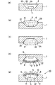
図2は上記工程に加熱硬化時の粘度の低下率が極めて高い蛍光体分散樹脂を投入せざるを得ないときの半導体発光素子の完成品の状態を示したものである。この場合、キャビティ3内にキャビティ3の上面に対して凸形状に盛り上がった状態になるまで蛍光体分散樹脂6を充填したケース1を反転すると、蛍光体分散樹脂6は下方に向かって凸形状に膨らんだ状態になる。
FIG. 2 shows the state of the finished product of the semiconductor light-emitting device when a phosphor-dispersed resin having a very high viscosity reduction rate during heat curing must be added to the above process. In this case, when the
この状態で蛍光体分散樹脂6が加熱されて低粘度になると、蛍光体分散樹脂6を構成する蛍光体5が蛍光体分散樹脂6の下方に向かって凸形状に膨らんだ最下部に向かって沈降するが、キャビティ3の内周面付近においては傾斜した反射面に沿って滑り落ちるように沈降する。その結果、蛍光体5が堆積した高密度蛍光体層8は中心部12に対して周辺部13が薄く形成され、色ムラ、輝度バラツキのある光源となることがある。
When the phosphor-dispersed
図3は加熱硬化時の粘度の低下率が極めて高い蛍光体分散樹脂を投入しても上記問題を生じないような構造の半導体発光装置を示したもので、以下に実施例2として説明する。 FIG. 3 shows a semiconductor light emitting device having a structure that does not cause the above problem even when a phosphor-dispersed resin having a very high viscosity reduction rate during heat curing is introduced.
図3(a)〜(e)は本発明の半導体発光装置の製造方法の実施例2を示す工程図である。実施例2はケースに形成されるキャビティが二つの部分で構成されている点が異なるだけで、製造工程は上記実施例1と同様である。 3A to 3E are process diagrams showing Example 2 of the method for manufacturing a semiconductor light emitting device of the present invention. The second embodiment differs from the first embodiment only in that the cavity formed in the case is composed of two parts.
以下に、上記実施例1で説明した内容と重複する部分が多々あるが、実施例2の製造工程について説明する。まず、(a)に示すように高反射率の非透光性樹脂からなるケース1に内周面を反射面2とする擂鉢形状の第一のキャビティ22と、第一のキャビティ22の上方にあって第一のキャビティ22と共有面23を有し、内周面を略垂直に立ち上げた第二のキャビティ24とが形成されている。
In the following, there are many portions that overlap the contents described in the first embodiment, but the manufacturing process of the second embodiment will be described. First, as shown in (a), a bowl-shaped
そして、第一のキャビティ22の底部には半導体発光素子4が搭載されている。なお、半導体発光素子4を発光させるためには、半導体発光素子4のアノード電極とカソード電極との間に順方向電圧を印加することが必要であり、そのために半導体発光素子4のアノード電極及びカソード電極の夫々と外部に導出されて電源と接続される端子電極との間に電気的導通を図るための接続手段が施されているが、本実施例を示す図3においてはこれを省略する。
The semiconductor light emitting element 4 is mounted on the bottom of the
次に(b)に示すように、第一のキャビティ22内及び第二のキャビティ24内に第二のキャビティ24の上面に対して凸形状に盛り上がった状態になるまで透光性樹脂に波長変換部材となる蛍光体5を分散した蛍光体分散樹脂6を充填する。なお、蛍光体分散樹脂6を第二のキャビティ24の上面に対して盛り上げる度合は、蛍光体分散樹脂6と第二のキャビティ24の上面内縁部25との間の付着力及び蛍光体分散樹脂6の適度な粘性による表面張力によって蛍光体分散樹脂6が第一のキャビティ22内及び第二のキャビティ24内から漏れ出さない範囲内で必要に応じて設定される。
Next, as shown in (b), the wavelength conversion into a translucent resin is performed in the
次に(c)に示すように、ケース1を反転させて第一のキャビティ22内及び第二のキャビティ24内に充填した蛍光体分散樹脂6を加熱硬化させる。なお、蛍光体分散樹脂6と第二のキャビティ24の上面内縁部25との間の付着力及び蛍光体分散樹脂6の適度な粘性による表面張力がケース1を反転させたときに蛍光体分散樹脂6に作用する重力に対抗する作用となって蛍光体分散樹脂6が第1のキャビティ22及び第二のキャビティ24にから漏れるのを阻止する。従って、蛍光体分散樹脂6の漏れ防止用の蓋は不要である。
Next, as shown in (c), the
ケース1を反転した状態で第1のキャビティ22内及び第二のキャビティ24内に充填した蛍光体分散樹脂6が硬化する過程において(d)に示すように、蛍光体分散樹脂6を構成する透光性樹脂と蛍光体5との比重差によって透光性樹脂よりも比重が大きい蛍光体5が沈降して蛍光体分散樹脂6の表面付近に堆積し、透光性樹脂に分散された蛍光体5の密度が高い高密度蛍光体層8と蛍光体5の密度が低いか又は蛍光体5が殆んど存在しない低密度蛍光体層9とに分離される。
In the process of curing the
このとき、蛍光体分散樹脂6が加熱されて極めて低粘度状態になると、蛍光体分散樹脂6内に分散された蛍光体5が蛍光体分散樹脂6の下方に向かって凸形状に膨らんだ最下部に向かって沈降するが、第二のキャビティ24が内周面を略垂直に立ち上げた状態に形成されているために高密度蛍光体層8の周辺部13は第二のキャビティ24の略垂直に立ち上げた内周面に沿って蛍光体が5堆積するので周辺部13であっても中心部12と略均一な厚みに高密度蛍光体層8が形成される。
At this time, when the
そして、(e)に示す半導体発光装置20が完成する。ここで本実施例の半導体発光装置20の光学系について説明する。半導体発光素子4から発せられて低密度蛍光体層9内を導光されて直接に高密度蛍光体層8に至った光のうち一部はそのまま高密度蛍光体層8の光出射面10から外部に放出され、一部は高密度蛍光体層8の蛍光体5で波長変換されて高密度蛍光体層8の光出射面10から外部に放出される。
Then, the semiconductor
また、半導体発光素子4から発せられて第一のキャビティ22の反射面2に向かう光は低密度蛍光体層9内を導光されて反射面2に至り、反射面2で高密度蛍光体層8方向に反射されて更に低密度蛍光体層9内を導光されて高密度蛍光体層8に至る。そして高密度蛍光体層8に至った光は上記同様に、そのうちの一部はそのまま高密度蛍光体層8の光出射面10から外部に放出され、一部は高密度蛍光体層8の蛍光体5で波長変換されて高密度蛍光体層8の光出射面10から外部に放出される。
Further, the light emitted from the semiconductor light emitting element 4 and directed to the
このように、半導体発光素子4から発せられて外部に放出される光は二つの光路を辿るため、半導体発光素子4から放出される光の量は二つの光路を辿って放出された光の量を合算したものになり、よって、光取り出し効率の高い明るい光源が実現できる構造になっている。 Thus, since the light emitted from the semiconductor light emitting element 4 and emitted to the outside follows two optical paths, the amount of light emitted from the semiconductor light emitting element 4 is the amount of light emitted along the two optical paths. Therefore, a bright light source with high light extraction efficiency can be realized.
また、高密度蛍光体層8の光出射面10から放出される光は、半導体発光素子4から発せられた光と半導体発光素子4から発せられて蛍光体5によって波長変換された光の2種であり、視覚的にはこの2種の光の加法混色の色調として認識される。
The light emitted from the
また、蛍光体分散樹脂6の表面付近に形成される高密度蛍光体層8は蛍光体5がケース1を反転させたときの重力で自然に沈降することによって形成され、且つ高密度蛍光体層8の周辺部13は第二のキャビティ24の略垂直に立ち上げた内周面に沿って蛍光体が5堆積するので周辺部13であっても中心部12と略均一な厚みに高密度蛍光体層8が形成されるために、高密度蛍光体層8の全面に亘ってほぼ均一な厚みで形成される。よって、高密度蛍光体層8内に入射した光は高密度蛍光体層8の光出射面10に至るまでの光路長が全面に亘ってほぼ同一になり、高密度蛍光体層8内に入射して蛍光体5によって波長変換される確率がほぼ等しくなるために、色ムラ、輝度バラツキが大幅に改善された光源を実現することができる。
The high-
また、外部に光を放出する光出射面10を構成する高密度蛍光体層8が凸形状に立体的に形成されているため、色調及び輝度が光の放射方向に殆んど依存しない光源となっている。
In addition, since the high-
更に、半導体発光素子4の光出射面11と界面を形成する低密度蛍光体層9は蛍光体5の密度が低いか又は蛍光体5が殆んど存在しない透光性樹脂であり、且つこの透光性樹脂は半導体発光素子4の光出射面11を構成する半導体材料に近い屈折率を有する部材を採用している。そして、半導体発光素子4内で発光した光のうち、半導体発光素子4の光出射面11で全反射して半導体発光素子4内に戻る光を極力少なくし、出来る限り多くの光を半導体発光素子4の光出射面11から界面を形成する低密度蛍光体層9内に出射させることによって半導体発光素子4からの光取り出し効率を高めたものである。
Further, the low-
ここで、実施例1及び実施例2に共通する事項を説明する。まず、半導体発光素子及び半導体発光素子のアノード電極及びカソード電極の夫々と外部に導出されて電源に接続される端子電極との間の電気的導通を図るための接続手段の1つであるボンディングワイヤ(図示せず)を透光性樹脂によって封止する目的は、半導体発光素子及びボンディングワイヤを振動、衝撃等の機械的応力や水分、ガス、塵埃などの外部環境から保護すると同時に、半導体発光素子の光出射面と界面を形成する部材に半導体発光素子の出射面を形成している半導体材料の屈折率に近いか或いはできればそれ以上の屈折率を有する材料を採用することによって、半導体発光素子内で発光した光のうち、半導体発光素子の光出射面で全反射して半導体発光素子内に戻る光を極力少なくし、出来る限り多くの光を半導体発光素子の光出射面から界面を形成する部材に出射させて半導体発光素子からの光取り出し効率を高めるためのものである。 Here, matters common to the first and second embodiments will be described. First, a bonding wire which is one of connection means for achieving electrical continuity between the semiconductor light emitting element and each of the anode electrode and the cathode electrode of the semiconductor light emitting element and a terminal electrode led to the outside and connected to a power source The purpose of sealing (not shown) with a translucent resin is to protect the semiconductor light emitting device and the bonding wire from mechanical environment such as vibration and impact, and external environment such as moisture, gas, dust and the like, and at the same time By adopting a material having a refractive index close to or higher than that of the semiconductor material forming the light emitting surface of the semiconductor light emitting element as a member that forms an interface with the light emitting surface of the semiconductor light emitting element, Among the light emitted from the semiconductor light emitting device, the light that is totally reflected by the light emitting surface of the semiconductor light emitting device and returns to the inside of the semiconductor light emitting device is minimized, and as much light as possible is transmitted to the semiconductor light emitting device. Of was emitted from the light emitting surface member forming the interface with in order to increase the light extraction efficiency from the semiconductor light emitting element.
また、高密度の蛍光体層を半導体発光装置が大気中に光を放出する面付近に形成する目的は、一つには、半導体発光装置から発せられて蛍光体で波長変換されて大気中に放出される光及び半導体発光装置から発せられてそのまま大気中に放出される光を出来る限り均一に散乱、屈折させて色ムラ、輝度バラツキの少ない光源を実現するためである。また一つには、蛍光体で波長変換された光の光取り出し効率を高めることにある。 The purpose of forming a high-density phosphor layer in the vicinity of the surface where the semiconductor light emitting device emits light into the atmosphere is, in part, the wavelength emitted from the semiconductor light emitting device and wavelength-converted by the phosphor. This is because the emitted light and the light emitted from the semiconductor light emitting device and emitted as it is into the atmosphere are scattered and refracted as uniformly as possible to realize a light source with less color unevenness and luminance variation. Another is to increase the light extraction efficiency of the light wavelength-converted by the phosphor.
つまり、半導体発光装置の外部に対する光出射面付近は高密度の蛍光体層が形成されており、光出射面は蛍光体によって凸凹模様の表面性状に形成されている。従って、半導体発光素子から発せられて蛍光体で波長変換された光及び半導体発光素子から発せられたそのままの光は凸凹模様の表面性状の光出射面で偏りが少なく、全方位に対して平均化された散乱、屈折が行われる。また、光出射面の凸部を形成する蛍光体で波長変換された光は大気中に放出されるまでに(蛍光体を覆う樹脂の被膜以外の)余計な介在物がなくそのまま大気中に放出されるために全反射及び屈折を受けることが少なく、光取り出し効率が良好な構造となっている。 That is, a high-density phosphor layer is formed in the vicinity of the light emission surface with respect to the outside of the semiconductor light emitting device, and the light emission surface is formed by the phosphor into a surface texture with a concavo-convex pattern. Therefore, the light emitted from the semiconductor light emitting element and wavelength-converted by the phosphor and the light as it is emitted from the semiconductor light emitting element have little unevenness on the light emitting surface having the surface texture of the uneven pattern, and are averaged over all directions. Scattering and refraction are performed. In addition, the light whose wavelength has been converted by the phosphor forming the convex portion of the light emitting surface is released into the atmosphere without any extra inclusions (other than the resin film covering the phosphor) before being emitted into the atmosphere. Therefore, it is less subject to total reflection and refraction, and has a structure with good light extraction efficiency.
ここで、本発明の半導体発光装置の効果について説明する。
(1)半導体発光素子及びボンディングワイヤを半導体発光素子の出射面を形成する半導体材料に近い屈折率を有する透光性樹脂で全面封止することで、半導体発光素子及びボンディングワイヤを振動、衝撃等の機械的応力や水分、ガス、塵埃などの外部環境から保護すると同時に、半導体発光素子内で発光した光のうち、半導体発光素子の光出射面で全反射して半導体発光素子内に戻る光を極力少なくし、出来る限り多くの光を半導体発光素子の光出射面から界面を形成する透光性樹脂に出射させることによって半導体発光素子からの光取り出し効率を高めた。
Here, the effect of the semiconductor light emitting device of the present invention will be described.
(1) The semiconductor light emitting element and the bonding wire are completely sealed with a translucent resin having a refractive index close to that of the semiconductor material forming the emission surface of the semiconductor light emitting element, so that the semiconductor light emitting element and the bonding wire are vibrated, shocked, etc. In addition to protecting from the external environment such as mechanical stress, moisture, gas, dust, etc., the light emitted from the semiconductor light emitting element is totally reflected by the light emitting surface of the semiconductor light emitting element and returns to the semiconductor light emitting element. The light extraction efficiency from the semiconductor light emitting element was increased by emitting as much light as possible from the light emitting surface of the semiconductor light emitting element to the translucent resin that forms the interface.
(2)キャビティ内にキャビティの最上面に対して凸形状に盛り上がった状態になるまで蛍光体分散樹脂を充填して反転硬化することにより、キャビティ内に充填された蛍光体分散樹脂の下方に向かって凸形状に膨らんだ表面付近に蛍光体が沈降して高密度の蛍光体層が形成される。その結果、高密度の蛍光体層の厚みも全面に亘って略均一に形成され、色ムラ、輝度バラツキの少ない光源となる。 (2) The phosphor dispersion resin is filled into the cavity until it rises in a convex shape with respect to the uppermost surface of the cavity, and is inverted and cured, so that the phosphor dispersion resin filled in the cavity faces downward. As a result, the phosphor settles near the surface bulging in a convex shape to form a high-density phosphor layer. As a result, the thickness of the high-density phosphor layer is substantially uniform over the entire surface, and the light source has less color unevenness and luminance variation.
(3)上記(2)の手法で蛍光体分散樹脂の表面付近に高密度蛍光体層が形成されることにより、外部に光を放出する光出射面を構成する高密度蛍光体層8がアーチ形状に立体的に形成されるため、色調及び輝度が光の放射方向に殆んど依存しない光源となる。
(3) When the high-density phosphor layer is formed in the vicinity of the surface of the phosphor-dispersed resin by the method of (2) above, the high-
(4)高密度の蛍光体層は光出射面付近に形成されており、蛍光体によって凸凹模様の表面性状に形成されている。従って、半導体発光素子から発せられて蛍光体で波長変換された光及び半導体発光素子から発せられたそのままの光は凸凹模様の表面性状の光出射面で偏りが少なく、全方位に対して平均化された散乱、屈折が行われる。また、光出射面の凸部を形成する蛍光体で波長変換された光は大気中に放出されるまでに(蛍光体を覆う樹脂の被膜以外の)余計な介在物がなくそのまま大気中に放出されるために全反射及び屈折を受けることが少なく、光取り出し効率が良好な構造になっている。 (4) The high-density phosphor layer is formed in the vicinity of the light exit surface, and is formed into a surface texture with an uneven pattern by the phosphor. Therefore, the light emitted from the semiconductor light emitting element and wavelength-converted by the phosphor and the light as it is emitted from the semiconductor light emitting element have little unevenness on the light emitting surface having the surface texture of the uneven pattern, and are averaged over all directions. Scattering and refraction are performed. In addition, the light whose wavelength has been converted by the phosphor forming the convex portion of the light emitting surface is released into the atmosphere without any extra inclusions (other than the resin film covering the phosphor) before being emitted into the atmosphere. Therefore, the structure is less subject to total reflection and refraction, and has a good light extraction efficiency.
(5)第一のキャビティの上方に設けられた第二のキャビティが内周面を略垂直に立ち上げた状態に形成されており、反転硬化時に高密度蛍光体層の周辺部は第二のキャビティの略垂直に立ち上げた内周面に沿って蛍光体が堆積するので周辺部であっても中心部と略均一な厚みに高密度蛍光体層が形成される。特に、加熱硬化時の粘度の低下率が極めて高い蛍光体分散樹脂を投入する場合に有効な構造である。 (5) The second cavity provided above the first cavity is formed in a state where the inner peripheral surface is raised substantially vertically, and the periphery of the high-density phosphor layer is the second portion during reverse curing. Since the phosphor is deposited along the inner peripheral surface raised substantially perpendicular to the cavity, the high-density phosphor layer is formed in a substantially uniform thickness with the central portion even in the peripheral portion. In particular, this structure is effective when a phosphor-dispersed resin having a very high viscosity reduction rate upon heat curing is used.
(6)キャビティ内への蛍光体分散樹脂の充填は1回で良く、また蛍光体分散樹脂の反転硬化時のキャビティからの樹脂漏れ防止のための蓋も必要ないために、余分な工数を増やす必要がなく、製造コストの増加を抑制することができる。 (6) Filling the cavity with the phosphor-dispersed resin may be performed only once, and a lid for preventing resin leakage from the cavity at the time of reversal curing of the phosphor-dispersed resin is not necessary, so that extra man-hours are increased. There is no need, and an increase in manufacturing cost can be suppressed.
(7)本発明の半導体発光装置の外部に対する光出射面付近は高密度蛍光体層が全面に亘って略均一に形成されており、半導体発光素子から発せられた光が一定の範囲内からまとまって外部に放出されることはない。従って、直接人間の目に入っても悪影響を及ぼす恐れは殆んどなく、人に優しい光源となっている。などの優れた効果を奏するものである。 (7) A high-density phosphor layer is formed substantially uniformly over the entire surface of the light emitting surface with respect to the outside of the semiconductor light emitting device of the present invention, and the light emitted from the semiconductor light emitting element is collected from a certain range. Are not released to the outside. Therefore, even if it directly enters human eyes, there is almost no risk of adverse effects, and it is a human-friendly light source. It has excellent effects such as.
1 ケース
2 反射面
3 キャビティ
4 半導体発光素子
5 蛍光体
6 蛍光体分散樹脂
7 上面内縁部
8 高密度蛍光体層
9 低密度蛍光体層
10 光出射面
11 光出射面
12 中心部
13 周辺部
20 半導体発光装置
22 第一のキャビティ
23 共有面
24 第二のキャビティ
25 上面内縁部
DESCRIPTION OF
Claims (7)
前記キャビティの底部に少なくとも1つの半導体発光素子を搭載する工程と、
前記キャビティ内に波長変換部材を分散した透光性樹脂を充填する工程と、
前記キャビティ内に前記波長変換部材を分散した透光性樹脂が充填されたケースを反転して前記波長変換部材を分散した透光性樹脂を硬化する工程と、
を有することを特徴とする半導体発光装置の製造方法。 Preparing a case in which a concave cavity having an opening is formed;
Mounting at least one semiconductor light emitting device on the bottom of the cavity;
Filling a translucent resin in which a wavelength conversion member is dispersed in the cavity;
Reversing the case filled with the translucent resin in which the wavelength conversion member is dispersed in the cavity and curing the translucent resin in which the wavelength conversion member is dispersed;
A method of manufacturing a semiconductor light emitting device, comprising:
Priority Applications (4)
| Application Number | Priority Date | Filing Date | Title |
|---|---|---|---|
| JP2004106643A JP4229447B2 (en) | 2004-03-31 | 2004-03-31 | Semiconductor light emitting device and manufacturing method |
| US11/093,039 US7635873B2 (en) | 2004-03-31 | 2005-03-30 | Semiconductor light emitting device and method of manufacturing the same |
| DE102005014472A DE102005014472A1 (en) | 2004-03-31 | 2005-03-30 | Semiconductor light emitting device and method for its production |
| US12/643,871 US7955878B2 (en) | 2004-03-31 | 2009-12-21 | Semiconductor light emitting device and method of manufacturing the same |
Applications Claiming Priority (1)
| Application Number | Priority Date | Filing Date | Title |
|---|---|---|---|
| JP2004106643A JP4229447B2 (en) | 2004-03-31 | 2004-03-31 | Semiconductor light emitting device and manufacturing method |
Publications (2)
| Publication Number | Publication Date |
|---|---|
| JP2005294484A true JP2005294484A (en) | 2005-10-20 |
| JP4229447B2 JP4229447B2 (en) | 2009-02-25 |
Family
ID=35059680
Family Applications (1)
| Application Number | Title | Priority Date | Filing Date |
|---|---|---|---|
| JP2004106643A Expired - Fee Related JP4229447B2 (en) | 2004-03-31 | 2004-03-31 | Semiconductor light emitting device and manufacturing method |
Country Status (3)
| Country | Link |
|---|---|
| US (2) | US7635873B2 (en) |
| JP (1) | JP4229447B2 (en) |
| DE (1) | DE102005014472A1 (en) |
Cited By (14)
| Publication number | Priority date | Publication date | Assignee | Title |
|---|---|---|---|---|
| WO2007077869A1 (en) * | 2006-01-04 | 2007-07-12 | Rohm Co., Ltd. | Thin-type light emitting diode lamp, and its manufacturing |
| JP2007184330A (en) * | 2006-01-04 | 2007-07-19 | Rohm Co Ltd | Light emitting device and manufacturing method thereof |
| JP2007184326A (en) * | 2006-01-04 | 2007-07-19 | Rohm Co Ltd | Thin light emitting diode lamp and manufacturing method thereof |
| JP2008034833A (en) * | 2006-06-27 | 2008-02-14 | Mitsubishi Chemicals Corp | Lighting device |
| WO2010021346A1 (en) * | 2008-08-20 | 2010-02-25 | 三菱化学株式会社 | Semiconductor light emitting device and method for manufacturing the same |
| JP2012503334A (en) * | 2008-09-16 | 2012-02-02 | オスラム・シルバニア・インコーポレイテッド | Optical disc for lighting module |
| JP2012238619A (en) * | 2006-08-25 | 2012-12-06 | Philips Lumileds Lightng Co Llc | Backlight using high-powered corner led |
| JP2013225597A (en) * | 2012-04-23 | 2013-10-31 | Mitsubishi Electric Corp | Method of manufacturing light-emitting device, and light-emitting device |
| US8710741B2 (en) | 2006-06-27 | 2014-04-29 | Mitsubishi Chemical Corporation | Illuminating device |
| US8766298B2 (en) | 2006-09-01 | 2014-07-01 | Cree, Inc. | Encapsulant profile for light emitting diodes |
| JP2014175362A (en) * | 2013-03-06 | 2014-09-22 | Toshiba Corp | Semiconductor light-emitting element and method of manufacturing the same |
| JP2017092258A (en) * | 2015-11-10 | 2017-05-25 | 株式会社カネカ | Remote phosphor type semiconductor light emitting device and method of manufacturing the same |
| JP2017117912A (en) * | 2015-12-24 | 2017-06-29 | 日亜化学工業株式会社 | Light emitting device using wavelength converting member, and wavelength converting member and method for manufacturing light emitting device |
| JP2017135427A (en) * | 2010-12-28 | 2017-08-03 | 日亜化学工業株式会社 | Light emitting device |
Families Citing this family (20)
| Publication number | Priority date | Publication date | Assignee | Title |
|---|---|---|---|---|
| DE102005046420B4 (en) * | 2004-10-04 | 2019-07-11 | Stanley Electric Co. Ltd. | A method of manufacturing a semiconductor light-emitting device |
| JP2007273562A (en) * | 2006-03-30 | 2007-10-18 | Toshiba Corp | Semiconductor light emitting device |
| US7889421B2 (en) | 2006-11-17 | 2011-02-15 | Rensselaer Polytechnic Institute | High-power white LEDs and manufacturing method thereof |
| US20080192458A1 (en) * | 2007-02-12 | 2008-08-14 | Intematix Corporation | Light emitting diode lighting system |
| TW201007091A (en) * | 2008-05-08 | 2010-02-16 | Lok F Gmbh | Lamp device |
| US8807799B2 (en) * | 2010-06-11 | 2014-08-19 | Intematix Corporation | LED-based lamps |
| CN101916806A (en) * | 2010-06-18 | 2010-12-15 | 深圳市瑞丰光电子股份有限公司 | LED packaging method and LED packaging structure packaged by the method |
| JP5437177B2 (en) * | 2010-06-25 | 2014-03-12 | パナソニック株式会社 | Light emitting device |
| CN101980385A (en) * | 2010-07-19 | 2011-02-23 | 宁波市瑞康光电有限公司 | Method for encapsulating light-emitting diode (LED), LED and LED illumination device |
| TW201218428A (en) * | 2010-10-25 | 2012-05-01 | Hon Hai Prec Ind Co Ltd | Light emitting diode package structure |
| US20120236529A1 (en) * | 2011-03-15 | 2012-09-20 | Avago Technologies Ecbu Ip(Singapore) Pte. Ltd. | Method And Apparatus For A Light Source |
| US9041046B2 (en) | 2011-03-15 | 2015-05-26 | Avago Technologies General Ip (Singapore) Pte. Ltd. | Method and apparatus for a light source |
| US8492746B2 (en) | 2011-09-12 | 2013-07-23 | SemiLEDs Optoelectronics Co., Ltd. | Light emitting diode (LED) dice having wavelength conversion layers |
| JP5856816B2 (en) * | 2011-11-14 | 2016-02-10 | 株式会社小糸製作所 | Light emitting device |
| CN102593320B (en) * | 2012-02-08 | 2014-08-13 | 杨罡 | Light emitting diode (LED) light source and packaging method thereof |
| US20140145584A1 (en) * | 2012-11-27 | 2014-05-29 | Avago Technologies General Ip (Singapore) Pte. Ltd. | Hemispherical remoter phosphor and methods of forming the same |
| CN104465936B (en) * | 2013-09-13 | 2017-05-24 | 展晶科技(深圳)有限公司 | Light emitting diode |
| DE102014108377A1 (en) * | 2014-06-13 | 2015-12-17 | Osram Opto Semiconductors Gmbh | Method for producing an optoelectronic component and optoelectronic component |
| JP6827404B2 (en) * | 2017-11-30 | 2021-02-10 | 三菱電機株式会社 | Semiconductor devices and power converters |
| KR102477355B1 (en) * | 2018-10-23 | 2022-12-15 | 삼성전자주식회사 | Carrier substrate and substrate processing apparatus using the same |
Citations (6)
| Publication number | Priority date | Publication date | Assignee | Title |
|---|---|---|---|---|
| JPH07111343A (en) * | 1993-10-13 | 1995-04-25 | Matsushita Electron Corp | Photoelectric device |
| JP3048368U (en) * | 1997-10-27 | 1998-05-06 | 興 陳 | Light emitting diode |
| JP2000228544A (en) * | 1999-02-05 | 2000-08-15 | Sharp Corp | Semiconductor light emitting device |
| JP2000315823A (en) * | 1999-04-30 | 2000-11-14 | Runaraito Kk | Light emitting diode and method of manufacturing the same |
| JP2003046133A (en) * | 2001-07-26 | 2003-02-14 | Matsushita Electric Works Ltd | Light emitting device and manufacturing method thereof |
| JP2003318448A (en) * | 2002-02-19 | 2003-11-07 | Nichia Chem Ind Ltd | Light emitting device and method for forming the same |
Family Cites Families (21)
| Publication number | Priority date | Publication date | Assignee | Title |
|---|---|---|---|---|
| DE29724847U1 (en) * | 1996-06-26 | 2004-09-30 | Osram Opto Semiconductors Gmbh | Light-emitting semiconductor component with luminescence conversion element |
| DE19638667C2 (en) * | 1996-09-20 | 2001-05-17 | Osram Opto Semiconductors Gmbh | Mixed-color light-emitting semiconductor component with luminescence conversion element |
| US6613247B1 (en) * | 1996-09-20 | 2003-09-02 | Osram Opto Semiconductors Gmbh | Wavelength-converting casting composition and white light-emitting semiconductor component |
| JP3065263B2 (en) | 1996-12-27 | 2000-07-17 | 日亜化学工業株式会社 | Light emitting device and LED display using the same |
| US6340824B1 (en) * | 1997-09-01 | 2002-01-22 | Kabushiki Kaisha Toshiba | Semiconductor light emitting device including a fluorescent material |
| US5959316A (en) * | 1998-09-01 | 1999-09-28 | Hewlett-Packard Company | Multiple encapsulation of phosphor-LED devices |
| WO2001008452A1 (en) * | 1999-07-23 | 2001-02-01 | Patent-Treuhand-Gesellschaft für elektrische Glühlampen mbH | Luminous substance for a light source and light source associated therewith |
| JP2001127346A (en) | 1999-10-22 | 2001-05-11 | Stanley Electric Co Ltd | Light emitting diode |
| JP3533438B2 (en) | 1999-11-29 | 2004-05-31 | 独立行政法人産業技術総合研究所 | Separation method of rare earth and zinc |
| JP2001196639A (en) | 2000-01-12 | 2001-07-19 | Sanyo Electric Co Ltd | LED light emitting device and method of manufacturing the same |
| JP2001210872A (en) | 2000-01-26 | 2001-08-03 | Sanyo Electric Co Ltd | Semiconductor light emitting device and method of manufacturing the same |
| JP2001345483A (en) | 2000-05-31 | 2001-12-14 | Toshiba Lighting & Technology Corp | Light emitting diode |
| JP3789747B2 (en) | 2000-11-15 | 2006-06-28 | 三洋電機株式会社 | Method for manufacturing light emitting device |
| JP3614776B2 (en) * | 2000-12-19 | 2005-01-26 | シャープ株式会社 | Chip component type LED and its manufacturing method |
| JP2003234511A (en) | 2002-02-06 | 2003-08-22 | Toshiba Corp | Semiconductor light emitting device and method of manufacturing the same |
| US6924514B2 (en) * | 2002-02-19 | 2005-08-02 | Nichia Corporation | Light-emitting device and process for producing thereof |
| US6791116B2 (en) * | 2002-04-30 | 2004-09-14 | Toyoda Gosei Co., Ltd. | Light emitting diode |
| JP3707688B2 (en) * | 2002-05-31 | 2005-10-19 | スタンレー電気株式会社 | Light emitting device and manufacturing method thereof |
| JP2004047748A (en) * | 2002-07-12 | 2004-02-12 | Stanley Electric Co Ltd | Light emitting diode |
| US7264378B2 (en) * | 2002-09-04 | 2007-09-04 | Cree, Inc. | Power surface mount light emitting die package |
| JP3717480B2 (en) * | 2003-01-27 | 2005-11-16 | ローム株式会社 | Semiconductor light emitting device |
-
2004
- 2004-03-31 JP JP2004106643A patent/JP4229447B2/en not_active Expired - Fee Related
-
2005
- 2005-03-30 DE DE102005014472A patent/DE102005014472A1/en not_active Ceased
- 2005-03-30 US US11/093,039 patent/US7635873B2/en not_active Expired - Fee Related
-
2009
- 2009-12-21 US US12/643,871 patent/US7955878B2/en not_active Expired - Fee Related
Patent Citations (6)
| Publication number | Priority date | Publication date | Assignee | Title |
|---|---|---|---|---|
| JPH07111343A (en) * | 1993-10-13 | 1995-04-25 | Matsushita Electron Corp | Photoelectric device |
| JP3048368U (en) * | 1997-10-27 | 1998-05-06 | 興 陳 | Light emitting diode |
| JP2000228544A (en) * | 1999-02-05 | 2000-08-15 | Sharp Corp | Semiconductor light emitting device |
| JP2000315823A (en) * | 1999-04-30 | 2000-11-14 | Runaraito Kk | Light emitting diode and method of manufacturing the same |
| JP2003046133A (en) * | 2001-07-26 | 2003-02-14 | Matsushita Electric Works Ltd | Light emitting device and manufacturing method thereof |
| JP2003318448A (en) * | 2002-02-19 | 2003-11-07 | Nichia Chem Ind Ltd | Light emitting device and method for forming the same |
Cited By (16)
| Publication number | Priority date | Publication date | Assignee | Title |
|---|---|---|---|---|
| JP2007184330A (en) * | 2006-01-04 | 2007-07-19 | Rohm Co Ltd | Light emitting device and manufacturing method thereof |
| JP2007184326A (en) * | 2006-01-04 | 2007-07-19 | Rohm Co Ltd | Thin light emitting diode lamp and manufacturing method thereof |
| WO2007077869A1 (en) * | 2006-01-04 | 2007-07-12 | Rohm Co., Ltd. | Thin-type light emitting diode lamp, and its manufacturing |
| US8004002B2 (en) | 2006-01-04 | 2011-08-23 | Rohm Co., Ltd. | Thin-light emitting diode lamp, and method of manufacturing the same |
| US8405112B2 (en) | 2006-01-04 | 2013-03-26 | Rohm Co., Ltd. | Thin-light emitting diode lamp, and method of manufacturing the same |
| US8710741B2 (en) | 2006-06-27 | 2014-04-29 | Mitsubishi Chemical Corporation | Illuminating device |
| JP2008034833A (en) * | 2006-06-27 | 2008-02-14 | Mitsubishi Chemicals Corp | Lighting device |
| JP2012238619A (en) * | 2006-08-25 | 2012-12-06 | Philips Lumileds Lightng Co Llc | Backlight using high-powered corner led |
| US8766298B2 (en) | 2006-09-01 | 2014-07-01 | Cree, Inc. | Encapsulant profile for light emitting diodes |
| WO2010021346A1 (en) * | 2008-08-20 | 2010-02-25 | 三菱化学株式会社 | Semiconductor light emitting device and method for manufacturing the same |
| JP2012503334A (en) * | 2008-09-16 | 2012-02-02 | オスラム・シルバニア・インコーポレイテッド | Optical disc for lighting module |
| JP2017135427A (en) * | 2010-12-28 | 2017-08-03 | 日亜化学工業株式会社 | Light emitting device |
| JP2013225597A (en) * | 2012-04-23 | 2013-10-31 | Mitsubishi Electric Corp | Method of manufacturing light-emitting device, and light-emitting device |
| JP2014175362A (en) * | 2013-03-06 | 2014-09-22 | Toshiba Corp | Semiconductor light-emitting element and method of manufacturing the same |
| JP2017092258A (en) * | 2015-11-10 | 2017-05-25 | 株式会社カネカ | Remote phosphor type semiconductor light emitting device and method of manufacturing the same |
| JP2017117912A (en) * | 2015-12-24 | 2017-06-29 | 日亜化学工業株式会社 | Light emitting device using wavelength converting member, and wavelength converting member and method for manufacturing light emitting device |
Also Published As
| Publication number | Publication date |
|---|---|
| JP4229447B2 (en) | 2009-02-25 |
| US20100099208A1 (en) | 2010-04-22 |
| DE102005014472A1 (en) | 2005-11-03 |
| US7955878B2 (en) | 2011-06-07 |
| US20050224818A1 (en) | 2005-10-13 |
| US7635873B2 (en) | 2009-12-22 |
Similar Documents
| Publication | Publication Date | Title |
|---|---|---|
| JP4229447B2 (en) | Semiconductor light emitting device and manufacturing method | |
| JP4504056B2 (en) | Manufacturing method of semiconductor light emitting device | |
| KR100631992B1 (en) | Side-emitting dual lens structure LED package | |
| US8039862B2 (en) | White light emitting diode package having enhanced white lighting efficiency and method of making the same | |
| US10305001B2 (en) | High-power white LEDs | |
| CN101800281B (en) | Semiconductor light emitting device | |
| CN100555681C (en) | Light emitting diode light source with lens | |
| JP2020072264A (en) | Lighting devices and lighting modules | |
| KR100998017B1 (en) | Lens for light emitting device package and light emitting device package having same | |
| TW200849499A (en) | Optoelectronic device with housing body | |
| CN101459163A (en) | Light emitting diode | |
| CN207338367U (en) | Light emitting diode and light emitting module | |
| US12546458B2 (en) | Backlight unit | |
| JP2013062393A (en) | Light emitting device | |
| JP6195760B2 (en) | LED light emitting device | |
| JP2004235337A (en) | Light emitting diode | |
| CN103730560A (en) | LED structure | |
| TWM456497U (en) | Light-emitting diode module | |
| US20190115718A1 (en) | Eye-safe light source and method for manufacturing same | |
| CN101252160A (en) | light emitting semiconductor device | |
| KR102432222B1 (en) | Optical plate, lighting device, and lighting module | |
| KR101334315B1 (en) | Light emitting diode lamp and method of fabricating the same | |
| KR101309758B1 (en) | Light emitting diode lamp and method of fabricating the same | |
| KR102531104B1 (en) | Optical plate, lighting device, and lighting module | |
| WO2014017261A1 (en) | Light emitting apparatus |
Legal Events
| Date | Code | Title | Description |
|---|---|---|---|
| A131 | Notification of reasons for refusal |
Free format text: JAPANESE INTERMEDIATE CODE: A131 Effective date: 20071127 |
|
| A521 | Request for written amendment filed |
Free format text: JAPANESE INTERMEDIATE CODE: A523 Effective date: 20080125 |
|
| A02 | Decision of refusal |
Free format text: JAPANESE INTERMEDIATE CODE: A02 Effective date: 20080812 |
|
| A521 | Request for written amendment filed |
Free format text: JAPANESE INTERMEDIATE CODE: A523 Effective date: 20080910 |
|
| A911 | Transfer to examiner for re-examination before appeal (zenchi) |
Free format text: JAPANESE INTERMEDIATE CODE: A911 Effective date: 20081016 |
|
| TRDD | Decision of grant or rejection written | ||
| A01 | Written decision to grant a patent or to grant a registration (utility model) |
Free format text: JAPANESE INTERMEDIATE CODE: A01 Effective date: 20081111 |
|
| A01 | Written decision to grant a patent or to grant a registration (utility model) |
Free format text: JAPANESE INTERMEDIATE CODE: A01 |
|
| A61 | First payment of annual fees (during grant procedure) |
Free format text: JAPANESE INTERMEDIATE CODE: A61 Effective date: 20081201 |
|
| R150 | Certificate of patent or registration of utility model |
Ref document number: 4229447 Country of ref document: JP Free format text: JAPANESE INTERMEDIATE CODE: R150 |
|
| FPAY | Renewal fee payment (event date is renewal date of database) |
Free format text: PAYMENT UNTIL: 20111212 Year of fee payment: 3 |
|
| FPAY | Renewal fee payment (event date is renewal date of database) |
Free format text: PAYMENT UNTIL: 20111212 Year of fee payment: 3 |
|
| FPAY | Renewal fee payment (event date is renewal date of database) |
Free format text: PAYMENT UNTIL: 20121212 Year of fee payment: 4 |
|
| R250 | Receipt of annual fees |
Free format text: JAPANESE INTERMEDIATE CODE: R250 |
|
| FPAY | Renewal fee payment (event date is renewal date of database) |
Free format text: PAYMENT UNTIL: 20121212 Year of fee payment: 4 |
|
| FPAY | Renewal fee payment (event date is renewal date of database) |
Free format text: PAYMENT UNTIL: 20131212 Year of fee payment: 5 |
|
| R250 | Receipt of annual fees |
Free format text: JAPANESE INTERMEDIATE CODE: R250 |
|
| R250 | Receipt of annual fees |
Free format text: JAPANESE INTERMEDIATE CODE: R250 |
|
| R250 | Receipt of annual fees |
Free format text: JAPANESE INTERMEDIATE CODE: R250 |
|
| R250 | Receipt of annual fees |
Free format text: JAPANESE INTERMEDIATE CODE: R250 |
|
| R250 | Receipt of annual fees |
Free format text: JAPANESE INTERMEDIATE CODE: R250 |
|
| R250 | Receipt of annual fees |
Free format text: JAPANESE INTERMEDIATE CODE: R250 |
|
| R250 | Receipt of annual fees |
Free format text: JAPANESE INTERMEDIATE CODE: R250 |
|
| R250 | Receipt of annual fees |
Free format text: JAPANESE INTERMEDIATE CODE: R250 |
|
| R250 | Receipt of annual fees |
Free format text: JAPANESE INTERMEDIATE CODE: R250 |
|
| R250 | Receipt of annual fees |
Free format text: JAPANESE INTERMEDIATE CODE: R250 |
|
| R250 | Receipt of annual fees |
Free format text: JAPANESE INTERMEDIATE CODE: R250 |
|
| LAPS | Cancellation because of no payment of annual fees |