JP2005294418A - Semiconductor device and manufacturing method thereof - Google Patents
Semiconductor device and manufacturing method thereof Download PDFInfo
- Publication number
- JP2005294418A JP2005294418A JP2004105182A JP2004105182A JP2005294418A JP 2005294418 A JP2005294418 A JP 2005294418A JP 2004105182 A JP2004105182 A JP 2004105182A JP 2004105182 A JP2004105182 A JP 2004105182A JP 2005294418 A JP2005294418 A JP 2005294418A
- Authority
- JP
- Japan
- Prior art keywords
- impurity
- region
- semiconductor device
- capacitor
- forming
- Prior art date
- Legal status (The legal status is an assumption and is not a legal conclusion. Google has not performed a legal analysis and makes no representation as to the accuracy of the status listed.)
- Pending
Links
Images

Landscapes
- Liquid Crystal (AREA)
- Semiconductor Integrated Circuits (AREA)
- Metal-Oxide And Bipolar Metal-Oxide Semiconductor Integrated Circuits (AREA)
- Thin Film Transistor (AREA)
Abstract
【課題】 製造工程を削減することができ、画素電極の電圧の低下を十分に抑止することができるGOLD構造の半導体装置およびその製造方法を提供する。
【解決手段】 本発明の半導体装置100は、n型TFT30とキャパシタ60とを備えた半導体装置であって、n型TFT30はソース領域30aおよびドレイン領域30bを有している。ソース領域30aおよびドレイン領域30bの各々は、n型TFT30のゲート電極12の真下に形成された第1不純物領域5b,5cと、第1不純物領域5b,5cの不純物濃度よりも高い不純物濃度を有する第2不純物領域5f,5gとを有している。第1不純物領域5b,5cの不純物濃度とキャパシタ60の一方電極8aの不純物濃度とが同じである。
【選択図】 図1PROBLEM TO BE SOLVED: To provide a semiconductor device having a GOLD structure capable of reducing a manufacturing process and sufficiently suppressing a decrease in voltage of a pixel electrode and a manufacturing method thereof.
A semiconductor device 100 of the present invention is a semiconductor device including an n-type TFT 30 and a capacitor 60, and the n-type TFT 30 has a source region 30a and a drain region 30b. Each of the source region 30a and the drain region 30b has an impurity concentration higher than the impurity concentration of the first impurity regions 5b and 5c formed immediately below the gate electrode 12 of the n-type TFT 30 and the first impurity regions 5b and 5c. Second impurity regions 5f and 5g are provided. The impurity concentration of first impurity regions 5b and 5c is the same as the impurity concentration of one electrode 8a of capacitor 60.
[Selection] Figure 1
Description
本発明は、半導体装置およびその製造方法に関し、より特定的には、トランジスタとキャパシタとを備えた半導体装置およびその製造方法に関する。 The present invention relates to a semiconductor device and a manufacturing method thereof, and more particularly to a semiconductor device including a transistor and a capacitor and a manufacturing method thereof.
近年、絶縁表面を有する基板上に形成された、厚さ数〜数百nm程度の半導体薄膜を用いて薄膜トランジスタ(TFT:Thin Film Transistor)を構成し、このTFTで形成した大面積集積回路を有する半導体装置の開発が進んでいる。アクティブマトリクス型液晶表示装置、EL表示装置、および密着型イメージセンサはその代表例として知られている。特に、ポリシリコン膜などの結晶質シリコン膜を活性層にしたTFTは電界効果移動度が高いことから、いろいろな機能回路を形成することも可能である。 In recent years, a thin film transistor (TFT) is formed using a semiconductor thin film with a thickness of about several to several hundreds of nanometers formed on a substrate having an insulating surface, and a large-area integrated circuit formed using this TFT is provided. Development of semiconductor devices is progressing. Active matrix liquid crystal display devices, EL display devices, and contact image sensors are known as representative examples. In particular, since a TFT using a crystalline silicon film such as a polysilicon film as an active layer has high field effect mobility, various functional circuits can be formed.
たとえば、アクティブマトリクス型液晶表示装置は、機能ブロックごとに画像表示を行なう画素回路と、CMOS(Complementary Metal Oxide Semiconductor)回路を基本としたシフトレジスタ回路、レベルシフタ回路、バッファ回路、サンプリング回路などの画素回路を制御するための駆動回路とが一枚の基板上に形成される。 For example, an active matrix liquid crystal display device includes a pixel circuit that displays an image for each functional block, and a pixel circuit such as a shift register circuit, a level shifter circuit, a buffer circuit, and a sampling circuit based on a complementary metal oxide semiconductor (CMOS) circuit. And a drive circuit for controlling the above are formed on a single substrate.
アクティブマトリクス型液晶表示装置の画素回路が設けられた基板には、数十から数百万個の画素の各々に画素TFTの各々が配置され、その画素TFTの各々に画素が設けられている。液晶を挟んで対向するもう一方の基板には対向電極が設けられており、液晶を誘電体とした一種のコンデンサを形成している。そして、画素の各々に印加する電圧をTFTのスイッチング機能により制御して、このコンデンサへの電荷の供給が制御される。これにより、液晶を駆動し、透過光量を制御して画像が表示される。 On the substrate on which the pixel circuit of the active matrix liquid crystal display device is provided, each pixel TFT is disposed in each of several tens to millions of pixels, and each pixel TFT is provided with a pixel. The other substrate facing the liquid crystal is provided with a counter electrode to form a kind of capacitor using the liquid crystal as a dielectric. Then, the voltage applied to each pixel is controlled by the switching function of the TFT, and the supply of electric charge to this capacitor is controlled. As a result, the liquid crystal is driven and the amount of transmitted light is controlled to display an image.
画素TFTはnチャネル型TFTからなり、スイッチング素子として液晶に電圧を印加して駆動させるものである。液晶は交流で駆動させるので、フレーム反転駆動と呼ばれる方式が多く採用されている。この方式では画面を書き換えるまでの1フレームの間、液晶に印加された電圧を保持する必要がある。画素TFTのオフ電流(TFTがオフ動作時に流れるドレイン電流)が大きいと、液晶に印加された電圧が時間とともに減少し、表示品質を劣化させることになる。このため、画素TFTのオフ電流値を低減することが求められている。 The pixel TFT is composed of an n-channel TFT, and is driven by applying a voltage to the liquid crystal as a switching element. Since the liquid crystal is driven by alternating current, a method called frame inversion driving is often employed. In this method, it is necessary to hold the voltage applied to the liquid crystal for one frame until the screen is rewritten. If the off-current of the pixel TFT (drain current flowing when the TFT is turned off) is large, the voltage applied to the liquid crystal decreases with time, and the display quality is deteriorated. For this reason, it is required to reduce the off-current value of the pixel TFT.
オフ電流値を低減することのできるTFTの構造として、LDD(Lightly Doped Drain)構造が知られている。LDD構造のTFTは、ソース領域およびドレイン領域の各々からチャネル形成領域側へ伸びた低濃度の不純物領域(LDD領域)の各々を有している。LDD構造のTFTによれば、ドレイン領域とチャネル形成領域との界面付近の電界を緩和することができるので、オフ電流値を低減することができる。また、LDD構造のTFTでは、ソース/ドレイン間の電界をLDD領域で緩和することでソース/ドレイン間の耐圧をある程度向上できるが、ソース/ドレイン間の耐圧はそれでもなお不十分であった。 An LDD (Lightly Doped Drain) structure is known as a TFT structure that can reduce the off-current value. The TFT having an LDD structure has low-concentration impurity regions (LDD regions) extending from the source region and the drain region to the channel formation region side. According to the LDD structure TFT, the electric field in the vicinity of the interface between the drain region and the channel formation region can be relaxed, so that the off-current value can be reduced. Further, in the TFT having the LDD structure, the source / drain breakdown voltage can be improved to some extent by relaxing the source / drain electric field in the LDD region, but the source / drain breakdown voltage is still insufficient.
そこで、ソース/ドレイン間の耐圧を一層向上することのできるTFTの構造として、GOLD(Gate Overlapped Lightly Doped Drain)構造が知られている。GOLD構造のTFTは、ソース領域およびドレイン領域から伸びた低濃度の不純物領域(GOLD領域)をゲート電極の真下のチャネル形成領域に有している。GOLD構造のTFTによれば、不純物の注入によりGOLD領域の閾値電圧が低下するので、ドレイン領域側の空乏層の形成が抑制される。したがって、ソース/ドレイン間の耐圧を向上することができる。 Therefore, a GOLD (Gate Overlapped Lightly Doped Drain) structure is known as a TFT structure that can further improve the breakdown voltage between the source and the drain. A TFT having a GOLD structure has a low-concentration impurity region (GOLD region) extending from a source region and a drain region in a channel formation region directly below a gate electrode. According to the TFT having the GOLD structure, the threshold voltage of the GOLD region is lowered by the impurity implantation, so that the formation of the depletion layer on the drain region side is suppressed. Therefore, the breakdown voltage between the source / drain can be improved.
また、GOLD構造のTFTによれば、TFTのオン動作時にソース/ドレイン間に流れる電流(オン電流)の低下を防ぐことができる。すなわち、通常のTFTでは、ゲートに比べてドレインに高電圧を印加すると、ドレイン側の接合部に大きな電界ができる。そして、この電界により加速された電子がインパクトイオン化現象を起こし、電子・正孔対を発生する。電子・正孔対のうち、電子は、ゲート酸化膜と半導体膜との間のエネルギー障壁を超えて、ゲート酸化膜中に注入される。そして、酸化膜中に入った電子は負の固定電荷となり、TFTの閾値電圧を正側へシフトさせる。その結果、TFTのオン電流の低下を招く。これに対し、GOLD構造のTFTによれば、ゲートに比べてドレインに高電圧を印加しても、ドレイン側の接合部に大きな電界が形成されない。このため、インパクトイオン化現象が起こりにくくなるので、TFTのオン電流の低下を抑止することができる。 Further, according to the GOLD structure TFT, it is possible to prevent the current flowing between the source and the drain (ON current) from being lowered during the ON operation of the TFT. That is, in a normal TFT, when a higher voltage is applied to the drain than to the gate, a large electric field is generated at the junction on the drain side. Electrons accelerated by this electric field cause an impact ionization phenomenon, generating electron / hole pairs. Of the electron / hole pairs, electrons are injected into the gate oxide film over the energy barrier between the gate oxide film and the semiconductor film. Then, electrons entering the oxide film become negative fixed charges, and the threshold voltage of the TFT is shifted to the positive side. As a result, the on-current of the TFT is reduced. On the other hand, with the GOLD structure TFT, even when a higher voltage is applied to the drain than the gate, a large electric field is not formed at the junction on the drain side. For this reason, the impact ionization phenomenon is less likely to occur, so that a decrease in the on-current of the TFT can be suppressed.
しかしながら、GOLD構造のTFTでは、ゲート電極下のチャネル形成領域にまで低濃度の不純物領域が形成されているので、チャネルが形成されやすくなり、GOLD領域の閾値電圧がチャネル部分に比べて低くなる。このため、オフ電流が流れやすくなり、オフ電流値が増加するという問題があった。このような問題は、GOLD構造とLDD構造とを有するTFTにも共通する問題であった。ここで、GOLD構造とLDD構造とを有するTFTとは、ソース領域およびドレイン領域よりも低濃度の不純物領域であるLDD領域を、ソース領域およびドレイン領域とチャネル形成領域との間に有しており、かつLDD領域よりもさらに低濃度のGOLD領域を、LDD領域とチャネル形成領域との間に有しているTFTである。 However, in the GOLD structure TFT, since a low-concentration impurity region is formed even in the channel formation region under the gate electrode, a channel is easily formed, and the threshold voltage of the GOLD region is lower than that of the channel portion. For this reason, there is a problem that an off-current easily flows and an off-current value increases. Such a problem is common to TFTs having a GOLD structure and an LDD structure. Here, a TFT having a GOLD structure and an LDD structure has an LDD region, which is an impurity region having a lower concentration than the source region and the drain region, between the source region and the drain region and the channel formation region. The TFT has a GOLD region having a lower concentration than the LDD region between the LDD region and the channel formation region.
オフ電流値が増加するというGOLD構造のTFTの問題を解決する方法として、画素の各々に印加する電圧を保持するためのキャパシタをさらに形成する方法がある。画素の各々に印加する電圧の低下量はオフ電流の量に比例し、キャパシタの容量に反比例する。したがって、この方法によれば、TFTのオン電流の低下を抑止しつつ、TFTのオフ電流による画素電極の電圧の低下をキャパシタに蓄積した電荷によって抑制することができる。 As a method of solving the problem of the GOLD structure TFT in which the off-current value increases, there is a method of further forming a capacitor for holding a voltage applied to each pixel. The amount of decrease in voltage applied to each pixel is proportional to the amount of off-current and inversely proportional to the capacitance of the capacitor. Therefore, according to this method, it is possible to suppress the decrease in the voltage of the pixel electrode due to the off current of the TFT by the charge accumulated in the capacitor while suppressing the decrease in the on current of the TFT.
なお、ソース領域およびドレイン領域が高濃度の不純物領域と低濃度の不純物領域とを有するTFTとの製造方法が、たとえば特開2001−345448号公報(特許文献1)に開示されている。また、MOS(Metal Oxide Semiconductor)キャパシタとGOLD構造のTFTとの製造方法が、たとえば特開2002−76351号公報(特許文献2)に開示されている。
キャパシタと、GOLD構造のTFTとを1つの基板上に形成しようとすると、その製造工程が複雑なものになり、工程数が増加してしまうという問題があった。 If the capacitor and the GOLD structure TFT are formed on one substrate, the manufacturing process becomes complicated, resulting in an increase in the number of processes.
ここで、特許文献2に開示された技術では、GOLD構造のTFTとMOSキャパシタとがほぼ同一の工程によって製造されている。MOSキャパシタとは、MOSトランジスタとほぼ同様の構成を有するキャパシタである。MOSキャパシタにおいては、MOSトランジスタのゲート電極となる部分がキャパシタの上部電極となり、MOSトランジスタのソース領域となる部分と、ドレイン領域となる部分と、チャネル形成領域となる部分とがキャパシタの下部電極となる。MOSキャパシタにおいては、キャパシタの上部電極に印加される電圧によってキャパシタの容量が大きく変化する。このため、安定してキャパシタに電荷を蓄積することができず、TFTのオフ電流による画素電極の電圧の低下を十分に抑止することができないという問題があった。
Here, in the technique disclosed in
したがって、本発明の目的は、製造工程を削減することができ、画素電極の電圧の低下を十分に抑止することができるGOLD構造の半導体装置およびその製造方法を提供することである。 Accordingly, an object of the present invention is to provide a semiconductor device having a GOLD structure that can reduce the number of manufacturing steps and sufficiently suppress a decrease in voltage of a pixel electrode, and a method for manufacturing the same.
本発明の半導体装置は、トランジスタとキャパシタとを備えた半導体装置であって、トランジスタはソース領域およびドレイン領域を有している。ソース領域およびドレイン領域の各々は、トランジスタのゲート電極の真下に形成された第1不純物領域と、第1不純物領域の不純物濃度よりも高い不純物濃度を有する第2不純物領域とを有している。第1不純物領域の不純物濃度とキャパシタの一方電極の不純物濃度とが同じである。 The semiconductor device of the present invention is a semiconductor device including a transistor and a capacitor, and the transistor has a source region and a drain region. Each of the source region and the drain region has a first impurity region formed immediately below the gate electrode of the transistor and a second impurity region having an impurity concentration higher than that of the first impurity region. The impurity concentration of the first impurity region is the same as the impurity concentration of one electrode of the capacitor.
本発明の半導体装置およびその製造方法によれば、1対の第1不純物領域を形成する工程と同一の工程により、第1不純物濃度を有するキャパシタの一方電極を形成することができる。したがって、半導体装置の製造工程を削減することができる。また、キャパシタの一方電極が1つの不純物領域で形成されるので、キャパシタの容量がキャパシタに印加される電圧によって変化しにくい。したがって、安定してキャパシタに電荷を蓄積することができ、画素電極の電圧の低下を十分に抑止することができる。 According to the semiconductor device and the manufacturing method thereof of the present invention, the one electrode of the capacitor having the first impurity concentration can be formed by the same process as the process of forming the pair of first impurity regions. Therefore, the manufacturing process of the semiconductor device can be reduced. In addition, since one electrode of the capacitor is formed of one impurity region, the capacitance of the capacitor hardly changes depending on the voltage applied to the capacitor. Accordingly, charges can be stably accumulated in the capacitor, and a decrease in the voltage of the pixel electrode can be sufficiently suppressed.
以下、本発明の実施の形態について、図に基づいて説明する。 Hereinafter, embodiments of the present invention will be described with reference to the drawings.
(実施の形態1)
図1は、本発明の実施の形態1における半導体装置の構成を示す断面図である。
(Embodiment 1)
FIG. 1 is a cross-sectional view showing the configuration of the semiconductor device according to the first embodiment of the present invention.
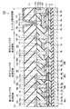
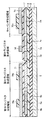
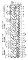
図1に示すように、本実施の形態の半導体装置100は、第1トランジスタ形成領域に形成されたGOLD構造とLDD構造とを有するn型TFT30と、第2トランジスタ形成領域に形成されたLDD構造のn型TFT40と、第3トランジスタ形成領域に形成されたp型TFT50と、キャパシタ形成領域に形成されたキャパシタ60とを備えている。
As shown in FIG. 1, a
基板1の上にSiN(窒化シリコン)膜2および下地膜3が積層して形成されている。n型TFT30は、ソース領域30aと、ドレイン領域30bと、チャネル形成領域5aとを第1トランジスタ形成領域の下地膜3の上に有している。ソース領域30aは、GOLD領域である第1不純物領域5bと、LDD領域である第3不純物領域5dと、第2不純物領域5fとを有している。ドレイン領域30bは、GOLD領域である第1不純物領域5cと、LDD領域である第3不純物領域5eと、第2不純物領域5gとを有している。第3の不純物領域5d,5eの各々は、第2の不純物領域5f,5gの各々からチャネル形成領域5aの方へ伸びるように形成されている。第1不純物領域5b,5cの各々は、第3の不純物領域5d,5eの各々からチャネル形成領域5aの方へ伸びるように形成されている。チャネル形成領域5aのチャネル長(図1中横方向の長さ)は、たとえば1
μmである。第3の不純物領域5d,5eの各々の不純物濃度は第1不純物領域5b,5cの各々の不純物濃度よりも高く、第2の不純物領域5g,5fの各々の不純物濃度は第3不純物領域5d,5eの各々の不純物濃度よりも高い。第1不純物領域5b,5cの各々はゲート電極12の真下に形成されている。すなわち、チャネル形成領域5aと、第1不純物領域5b,5cの各々とをゲート絶縁膜となるSiO2膜11を介して覆うように、n型TFT30のゲート電極12が形成されている。なお、第1不純物領域5b,5cの不純物濃度は1017原子/cm3以上1019原子/cm3以下であることが好ましい。
A SiN (silicon nitride)
μm. The impurity concentration of each of the
キャパシタ60は、下部電極8aと上部電極15とをキャパシタ形成領域の下地膜3上に有している。下部電極8aと上部電極15とは、誘電体となるSiO2膜11を挟んで互いに対向している。本実施の形態の半導体装置においては、キャパシタ60の下部電極8aの不純物濃度と、n型TFT30の第1不純物領域5b,5cの不純物濃度とが同じである。なお、下部電極8aの両側には中濃度不純物領域8b,8cの各々が形成されており、中濃度領域8b,8cの各々の両側には高濃度不純物領域8d,8eの各々が形成されている。
The
n型TFT40は、ソース領域40aと、ドレイン領域40bと、チャネル形成領域6aとを第2トランジスタ形成領域の下地膜3の上に有している。ソース領域40aは、LDD領域である第5不純物領域6bと、第4不純物領域6dとを有している。ドレイン領域30bは、LDD領域である第5不純物領域6cと、第4不純物領域6eとを有している。第5の不純物領域6b,6cの各々は、第4の不純物領域6d,6eの各々からチャネル形成領域5aの方へ伸びるように形成されている。第4の不純物領域6d,6eの各々の不純物濃度は第5不純物領域6b,6cの各々の不純物濃度よりも高い。チャネル形成領域6aをゲート絶縁膜となるSiO2膜11を介して覆うように、n型TFT40のゲート電極13が形成されている。
The n-
p型TFT50は、ソース領域7bと、ドレイン領域7cと、チャネル形成領域7aとを第3トランジスタ形成領域の下地膜3の上に有している。チャネル形成領域7aをゲート絶縁膜となるSiO2膜11を介して覆うように、p型TFT50のゲート電極14が形成されている。
The p-
ゲート電極12〜14と上部電極15とを覆うように、SiO2膜11上に層間絶縁膜16が形成されている。SiO2膜11および層間絶縁膜16には孔16a〜16hの各々が形成されており、孔16a〜16hの各々にはコンタクト17a〜17hの各々が形成されている。コンタクト17aとn型TFT30の第1不純物領域5fとは電気的に接続されており、コンタクト17bとn型TFT30の第1不純物領域5gとは電気的に接続されている。コンタクト17cとn型TFT40の第4不純物領域6dとは電気的に接続されており、コンタクト17dとn型TFT40の第4不純物領域6eとは電気的に接続されている。コンタクト17eとp型TFT50のソース領域7bとは電気的に接続されており、コンタクト17fとp型TFT50のドレイン領域7cとは電気的に接続されている。コンタクト17gとキャパシタ60の上部電極15とは電気的に接続されており、コンタクト17hとキャパシタ形成領域の高濃度不純物領域8eとは電気的に接続されている。
An interlayer insulating
コンタクト17a,17bの各々と電気的に接続するように、n型TFT30のソース電極19aおよびドレイン電極19bの各々が層間絶縁膜16上に形成されている。コンタクト17c,17dの各々と電気的に接続するように、n型TFT40のソース電極19cおよびドレイン電極19dの各々が層間絶縁膜16上に形成されている。コンタクト17e,17fの各々と電気的に接続するように、p型TFT50のソース電極19eおよびドレイン電極19fの各々が層間絶縁膜16上に形成されている。コンタクト17g,17hの各々と電気的に接続するように、配線19g,19hの各々が層間絶縁膜16上に形成されている。
Each of the
ソース電極19a,19c,19e、ドレイン電極19b,19d,19fおよび配線19g,19hの各々を覆うように、層間絶縁膜16上に層間絶縁膜21が形成されている。層間絶縁膜21には溝21aが形成されており、溝21aの内壁に沿うように画素電極22が形成されている。画素電極22と配線19gとは電気的に接続されている。配線19hには、配線19gよりも配線19hが低い電位となるような電圧が常に印加される。また、画素電極22は画素用トランジスタのドレイン領域と(図示なし)電気的に接続されている。
An interlayer insulating
本実施の形態の半導体装置100では、GOLD構造とLDD構造とを有するn型TFT30と、LDD構造のn型TFT40と、p型TFT50とが、各々の特性に応じて適切に配置される。具体的には、画素用トランジスタのように高電圧で駆動され、低いオフ電流が要求される部分にはGOLD構造とLDD構造とを有するn型TFT30が配置される。また、CMOS駆動回路のように多数のトランジスタを集積する部分には占有面積の小さいLDD構造のn型TFT40およびp型TFT50が配置される。
In the
なお、n型TFT30のゲート絶縁膜と、n型TFT40のゲート絶縁膜と、p型TFT50のゲート絶縁膜と、キャパシタ60の誘電体膜とは、連続したSiO2膜11で形成されている場合について示したが、本発明はこのような場合の他、ゲート絶縁膜とキャパシタの誘電体膜とが互いに分離していてもよい。また、n型TFT30のソース領域30aおよびドレイン領域30bおよびチャネル形成領域5a(以下、半導体膜)と、n型TFT40の半導体膜と、p型TFT50の半導体膜と、キャパシタ60の下部電極8aとが互いに分離している場合について示したが、本発明はこのような場合の他、これらの半導体膜とキャパシタの下部電極とが互いに連続していてもよい。
When the gate insulating film of the n-
続いて、本実施の形態の半導体装置の製造方法について説明する。 Subsequently, a method for manufacturing the semiconductor device of the present embodiment will be described.
図2〜図10は、本発明の実施の形態1における半導体装置の製造方法を工程順に説明する図である。 2 to 10 are views for explaining the semiconductor device manufacturing method according to the first embodiment of the present invention in the order of steps.
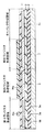
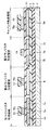
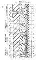
図2に示すように、たとえば1737ガラス(コーニング社製)よりなる基板1を準備する。そして、たとえば100nmの膜厚のSiN膜2と、たとえば100nmの膜厚のSiO2よりなる下地膜3とをプラズマCVD(Chemical Vapor Deposition)により基板1上に積層して形成する。ここで、SiN膜2は、基板1からの不純物が半導体膜へ拡散するのを防ぐために形成されるものである。SiNの代わりにSiON,SiC,AlN,Al2O3などを用いてもよい。また、SiN膜2と下地膜3とを省略してもよく、基板1上に他の下地膜をさらに積層してもよい。次に、アモルファスシリコン膜をプラズマCVDにより下地膜3上に形成し、アモルファスシリコン膜を真空中で熱処理する。この熱処理によってアモルファスシリコン中の不要な水素が除去される。次に、アモルファスシリコン膜にたとえばXeClレーザを照射することにより、アモルファスシリコン膜を多結晶シリコン膜に変える。多結晶シリコン膜中のシリコンの結晶粒径は約0.5μmとなる。なお、XeClレーザを照射する代わりに、たとえばYAG(Yttrium Aluminum Garnet)レーザやCW(Continuous Wave)レーザを照射してもよく、たとえばNi(ニッケル)などの触媒を用いて熱アニールを行なってもよい。次に、多結晶シリコン膜上にレジストをパターニングし、このレジストをマスクとして多結晶シリコン膜をドライエッチングする。これにより、半導体膜としての多結晶シリコン膜5〜8がアイランド状に形成される。その後、アッシングと薬液処理によりレジストを除去する。
As shown in FIG. 2, a
続いて、図3に示すように、多結晶シリコン膜5〜8を覆うようにたとえば100nmの膜厚のSiO2膜をプラズマCVDにより形成する。プラズマCVDの原料としてはたとえばTEOS(Tetra Ethyl Ortho Silicate)とO2とを用いる。次に、第1トランジスタ形成領域のSiO2膜11の一部と、第2および第3トランジスタ形成領域のSiO2膜11とを覆うようにレジスト70aを形成する。次に、レジスト70aをマスクとして、多結晶シリコン膜5と多結晶シリコン膜8とにたとえば1.3×10⁻¹⁷Jの加速エネルギで5×10¹²原子/cm2の注入量のP(リン)を注入する。これにより、多結晶シリコン膜5に第1不純物領域5b,5cが形成され、それと同時に、多結晶シリコン膜8にキャパシタ60の下部電極8aが形成される。なお、多結晶シリコン膜5における第1不純物領域5bと第1不純物領域5cとの間の領域は、チャネル形成領域5aとなる。
その後、アッシングと薬液処理によりレジスト70aを除去する。
Subsequently, as shown in FIG. 3, a SiO 2 film having a thickness of, for example, 100 nm is formed by plasma CVD so as to cover the
Thereafter, the resist 70a is removed by ashing and chemical treatment.
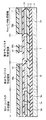
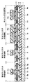
続いて、図4に示すように、たとえば200nmの膜厚のCr(クロム)よりなる導電膜71をスパッタ法により形成する。これにより、第1不純物領域5b,5cおよびチャネル形成領域6aの第1トランジスタ形成領域上にSiO2膜11を介して導電膜71が形成される。次に、第1および第2トランジスタ形成領域の導電膜71と、第3トランジスタ形成領域の導電膜71の一部と、キャパシタ形成領域の導電膜71とを覆うようにレジスト70bを形成する。次に、レジスト70bをマスクとして導電膜71をウエットエッチングする。これにより、p型TFT50のゲート電極14が形成される。その後、アッシングと薬液処理によりレジスト70bを除去する。
Subsequently, as shown in FIG. 4, a
続いて、図5に示すように、導電膜71をマスクとして、第3トランジスタ形成領域の多結晶シリコン膜7にたとえばB(ボロン)を注入する。これにより、多結晶シリコン膜7にソース領域7bおよびドレイン領域7cが形成される。多結晶シリコン膜7のソース領域7bとドレイン領域7cとの間の領域は、チャネル形成領域7aとなる。
Subsequently, as shown in FIG. 5, for example, B (boron) is implanted into the
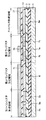
続いて、図6に示すように、チャネル形成領域5aと、第1不純物領域5b,5cの各々の一部とを覆うように、レジスト70cを導電膜71上に形成する。また、第2トランジスタ形成領域の一部と、キャパシタ形成領域の一部とを覆うように、レジスト70cを導電膜71上にも形成する。
Subsequently, as shown in FIG. 6, a resist 70c is formed on the
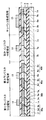
続いて、図7に示すように、レジスト70cをマスクとして、レジスト70cよりも線幅が細くなるように導電膜71をウエットエッチングする。ここで、「線幅」とは、チャネル長(図7中横方向)方向の長さである。これにより、チャネル形成領域5aと、第1不純物領域5b,5cの各々の一部とをSiO2膜11を介して覆うように、第1トランジスタのゲート電極12が形成される。ゲート電極12の形成と同時に、n型TFT40のゲート電極13が形成され、キャパシタ60の上部電極15が形成される。
Subsequently, as shown in FIG. 7, the
続いて、図8に示すように、レジスト70dを第3トランジスタ形成領域に形成する。そして、レジスト70c,70dをマスクとして、たとえば1.3×10⁻¹⁷Jの加速エネルギで1×10¹⁴原子/cm2の注入量のPを注入する。これにより、n型TFT30の第2不純物領域5f,5gが第1不純物領域5b,5c内に形成され、それと同時に、第4不純物領域6d,6eが多結晶シリコン膜6に形成される。さらに、下部電極8aの両端に高濃度不純物領域8d,8eも形成される。
Subsequently, as shown in FIG. 8, a resist 70d is formed in the third transistor formation region. Then, using the resists 70c and 70d as a mask, P having an implantation amount of 1 × 10 14 atoms / cm 2 is implanted with an acceleration energy of 1.3 × 10 −17 J, for example. Thereby, the
続いて、図9に示すように、アッシングと薬液処理によりレジスト70c,70dを除去する。そして、ゲート電極12〜14および上部電極15をマスクとして、たとえば1.3×10⁻¹⁷Jの加速エネルギで1×10¹³原子/cm2の注入量のPを注入する。このとき、ゲート電極12,13および上部電極15はレジスト70cよりも線幅が細くなっているので、ゲート電極12,13および上部電極15をマスクとして不純物を注入することにより、レジスト70cをマスクとしたときには不純物が注入されなかった領域にも不純物を注入することができる。これにより、第3不純物領域5d,5eが第1不純物領域5b,5c内に形成され、それと同時に、第5不純物領域6b,6cが多結晶シリコン膜6に形成される。なお、多結晶シリコン膜6の第5不純物領域6bと第5不純物領域6cとの間の領域は、チャネル形成領域6aとなる。さらに、下部電極8aの両端に中濃度不純物領域8b,8cも形成される。
Subsequently, as shown in FIG. 9, the resists 70c and 70d are removed by ashing and chemical treatment. Then, using the
続いて、図10に示すように、ゲート電極12〜14および上部電極15を覆うようにSiO2膜11上に層間絶縁膜16を形成する。次に、ソース領域30a,40a,7bの各々と、ドレイン領域30b,40b、7cの各々と、上部電極15の一部と、高濃度不純物領域8eとを露出するように、層間絶縁膜16に孔16a〜16hの各々を形成する。次に、孔16a〜16hの各々の内部にたとえばCrよりなるコンタクト17a〜17hの各々を形成する。ここで、高濃度不純物領域8eとコンタクト17hとを電気的に接続することにより、コンタクト17hのコンタクト抵抗を低減することができる。次に、ソース電極19a,19c,19e、ドレイン電極19b,19d,19fおよび配線19g,19hの各々をコンタクト17a〜17hの各々と電気的に接続するように層間絶縁膜16上に形成する。ソース電極19a,19c,19e、ドレイン電極19b,19d,19fおよび配線19g,19hは、たとえばAl(アルミニウム)により形成される。
Subsequently, as shown in FIG. 10, an
次に、図1に示すように、ソース電極19a,19c,19e、ドレイン電極19b,19d,19fおよび配線19g,19hの各々を覆うように、層間絶縁膜16上に層間絶縁膜21を形成する。次に、配線19gの一部を露出するように、層間絶縁膜21に溝21aを形成する。次に、溝21aの内壁面に沿って画素電極22を形成する。以上の工程により本実施の形態の半導体装置100が完成する。
Next, as shown in FIG. 1, an
本実施の形態の半導体装置100およびその製造方法によれば、GOLD領域である第1不純物領域5b,5cを形成する工程と同一の工程により、第1不純物領域5b,5cと同じ不純物濃度を有するキャパシタ60の下部電極8aを形成することができる。したがって、半導体装置の製造工程を削減することができる。また、キャパシタ60の下部電極8aが1つの不純物領域8aで形成されるので、キャパシタの容量がキャパシタに印加される電圧によって変化しにくい。したがって、安定してキャパシタに電荷を蓄積することができ、画素電極22の電圧の低下を十分に抑止することができる。
According to the
本実施の形態の半導体装置100においては、ソース領域30aおよびドレイン領域30bは第3不純物領域5d,5eを有している。第3の不純物領域5d,5eは第1不純物領域5b,5cと第2不純物領域5f,5gとの間に形成されており、第3不純物領域5d,5eの不純物濃度は、第1不純物領域5b,5cの不純物濃度よりも高く、第2の不純物領域5f,5gの不純物濃度よりも低い。
In
本実施の形態の半導体装置100の製造方法においては、第1不純物領域5b,5cよりも不純物濃度が高く、第2不純物領域5f,5gよりも不純物濃度が低い第3不純物領域5d,5eを第1不純物領域5b,5cと第2不純物領域5f,5gとの間に形成する。
In the method of manufacturing the
これにより、ソース領域30aおよびドレイン領域30bの各々がGOLD領域とLDD領域とを有するので、ドレイン領域30bとチャネル形成領域5aとの界面付近の電界を一層緩和することができる。その結果、n型TFT30のオフ電流値を一層低減することができる。
Thereby, since each of the
本実施の形態の半導体装置100においては、キャパシタ60の下部電極8aの電位よりもキャパシタ60の上部電極15の電位の方が常に高い。
In the
キャパシタの一方電極が不純物領域で形成される場合には、キャパシタの容量がキャパシタに印加される電圧により変化する。言い換えれば、キャパシタがC(容量)−V(電圧)特性を有する。キャパシタは、電圧が一定値以下の場合に電圧により容量が変化し、電圧が一定値以上になると容量が一定になるようなC−V特性を有している。容量が一定となる電圧をフラットバンド電圧という。特許文献2に開示された技術におけるキャパシタはMOSキャパシタであったので、フラットバンド電圧が正の大きな値となる。すなわち、下部電極の電位に対して上部電極の電位を高くしたとしても依然としてキャパシタの容量は電圧により変化する。一方、本実施の形態のキャパシタ60の下部電極は1つの不純物領域により形成されているので、フラットバンド電圧がマイナスの値となる。このため、下部電極8aの電位よりも上部電極15の電位を高く保つことにより、キャパシタ60の容量は電圧に関わらず一定となる。
When one electrode of the capacitor is formed of an impurity region, the capacitance of the capacitor changes depending on the voltage applied to the capacitor. In other words, the capacitor has C (capacitance) -V (voltage) characteristics. The capacitor has a CV characteristic such that when the voltage is below a certain value, the capacitance changes depending on the voltage, and when the voltage becomes above a certain value, the capacitance becomes constant. A voltage with a constant capacitance is called a flat band voltage. Since the capacitor in the technique disclosed in
本実施の形態の半導体装置100においては、キャパシタ60の上部電極15と画素電極20とが電気的に接続されている。
In the
これにより、画素電極20に印加する電圧の低下をキャパシタ60に蓄積した電荷によって抑制することができる。
As a result, a decrease in the voltage applied to the pixel electrode 20 can be suppressed by the charge accumulated in the
本実施の形態の半導体装置100において、第1不純物領域5b,5cの不純物濃度は1017原子/cm3以上1019原子/cm3以下である。
In the
これにより、n型TFT30の耐圧を向上することができる。また、第1不純物領域5b,5cの不純物濃度は1017原子/cm3以上とすることにより、キャパシタ60のフラットバンド電圧が正の値になる。すなわち、下部電極8aの電位よりも上部電極15の電位の方を高くすることによりキャパシタ60の容量を一定に保つことができる。
Thereby, the breakdown voltage of the n-
本実施の形態の半導体装置100の製造方法において、ゲート電極12は、多結晶シリコン膜5上にSiO2膜11を介して導電膜71を形成し、チャネル形成領域5aと、第1不純物領域5b,5cの各々の一部とを覆うように、レジスト70cを導電膜71上に形成し、レジスト70cをマスクとして、レジスト70cよりも線幅が細くなるように導電膜71をエッチングすることにより形成される。また、レジスト70cをマスクとして不純物を注入することにより第2不純物領域5f,5gが第1不純物領域5b,5c内に形成され、ゲート電極12をマスクとして不純物を注入することにより第3不純物領域5d,5eが形成される。
In the method of manufacturing the
これにより、簡易な方法によりゲート電極12と第2の不純物領域5f,5gと、第3の不純物領域5d,5eとが形成される。
Thereby, the
本実施の形態の半導体装置100の製造方法は、p型TFT40が以下の方法により形成される。導電膜71を形成すると同時に、半導体膜6上にSiO2膜11を介して導電膜71を形成する。レジスト70cを形成すると同時に、レジスト70cを第2トランジスタ形成領域の導電膜71上に形成する。導電膜71をエッチングすると同時に、レジスト70cをマスクとして、レジスト70cよりも線幅が細くなるように第2トランジスタ形成領域の導電膜71をエッチングする。第2不純物領域5f,5gを形成すると同時に、レジスト70cをマスクとして不純物を注入することにより第4不純物領域6d,6eを半導体層6に形成する。第3不純物領域5d,5eを形成すると同時に、ゲート電極13をマスクとして不純物を注入することにより第5不純物領域6b,6cを形成する。
In the manufacturing method of the
これにより、GOLD構造とLDD構造とを有するn型TFT30を形成すると同時に、LDD構造のn型TFT40を形成することができる。
Thereby, the n-
本実施の形態の半導体装置100においては、ゲート電極12を形成すると同時に、キャパシタ60の上部電極15を形成する。
In the
これにより、ゲート電極12と上部電極15とを別々の工程で形成する場合に比べて製造方法を簡略化できる。
Thereby, a manufacturing method can be simplified compared with the case where the
なお、本実施の形態においては、GOLD構造のTFTがn型TFT30である場合について示したが、本発明はこのような場合に限定されるものではなく、GOLD構造のTFTがpチャネル型トランジスタであってもよい。また、nチャネル型トランジスタであることが好ましい。
Note that although the case where the GOLD structure TFT is the n-
(実施の形態2)
図11は、本発明の実施の形態2における半導体装置の構成を示す断面図である。
(Embodiment 2)
FIG. 11 is a cross-sectional view showing the configuration of the semiconductor device according to the second embodiment of the present invention.
図11に示すように、本実施の形態の半導体装置101においては、第1トランジスタ形成領域にGOLD構造のn型TFT31が形成され、第2トランジスタ形成領域にn型TFT41が形成されている。n型TFT31は、ソース領域31aと、ドレイン領域31bと、チャネル形成領域5aとを第1トランジスタ形成領域の下地膜3の上に有している。ソース領域31aは、GOLD領域である第1不純物領域5bと、第2不純物領域5fとを有している。ドレイン領域31bは、GOLD領域である第1不純物領域5cと、第2不純物領域5gとを有している。第1不純物領域5b,5cの各々は、第2の不純物領域5f,5gの各々からチャネル形成領域5aの方へ伸びるようにゲート電極12の真下に形成されている。第2の不純物領域5f,5gの各々の不純物濃度は第1不純物領域5b,5cの各々の不純物濃度よりも高い。チャネル形成領域5aをゲート絶縁膜となるSiO2膜11を介して覆うように、n型TFT31のゲート電極12が形成されている。
As shown in FIG. 11, in the
n型TFT41は、ソース領域としての第4不純物領域6dと、ドレイン領域としての第4不純物領域6eと、チャネル形成領域6aとを第2トランジスタ形成領域の下地膜3の上に有している。チャネル形成領域6aをゲート絶縁膜となるSiO2膜11を介して覆うように、n型TFT41のゲート電極13が形成されている。
The n-
なお、これ以外の半導体装置101の構成は、図1に示す実施の形態1の半導体装置100の構成とほぼ同様であるので、同一の部材には同一の符号を付し、その説明を省略する。
Since the other configuration of the
続いて、本実施の形態の半導体装置の製造方法について説明する。 Subsequently, a method for manufacturing the semiconductor device of the present embodiment will be described.
本実施の形態の半導体装置101の製造方法は、まず図2〜図7に示す実施の形態1の製造工程とほぼ同様の製造工程を経る。次に、図8に示すようなレジスト70dをマスクとしたPの注入を行なわずにレジスト70dが除去される。その後、図9および図10に示す実施の形態1の製造工程とほぼ同様の製造工程を経て、本実施の形態の半導体装置101が完成する。
The manufacturing method of the
本実施の形態のように、GOLD構造のn型TFT31とn型TFT41とキャパシタ60とを備えた半導体装置101についても、本発明を適用することによって実施の形態1と同様の効果を得ることができる。
As in the present embodiment, the
以下本発明の実施例について説明する。 Examples of the present invention will be described below.
(実施例1)
本実施例においては、まず、図1に示す実施の形態1の半導体装置100を製造した。半導体装置100におけるn型TFT30のチャネル幅を10μmとし、チャネル長は5μmとした。また、第1不純物領域5b,5cのチャネル長方向の長さを1μmとし、第3不純物領域5d,5eのチャネル長方向の長さを0.5μmとした。また、ゲート電極12のチャネル長方向の長さを7μmとした。
(Example 1)
In this example, first, the
なお、本実施例では第1不純物領域5b,5cのチャネル長方向の長さを1μmとしたが、これは設計値である、実際の第1不純物領域5b,5cのチャネル長方向の長さは、ゲート電極12をマスクするレジスト70cのアライメント精度の影響を受ける。現状のステッパでは、第1不純物領域5b,5cのチャネル長方向の長さを1μmで設計すると、実際にはチャネル長方向の長さが1μm±0.3μmの第1不純物領域5b,5cの長さとなる。すなわち、第1不純物領域5b,5cのチャネル長方向の長さを0.7μm確保するためには、本実施例のように第1不純物領域5b,5cのチャネル長方向の長さを1μmで設計する必要がある。以上のように、第1不純物領域5b,5cのチャネル長方向の長さを設計する際には、ゲート電極12をマスクするレジスト70cのアライメント精度の影響を考慮する必要がある。
In this embodiment, the length of the
次に、第1不純物領域5b,5cおよび下部電極8aの不純物濃度と、第3不純物領域5d,5eの不純物濃度をSIMS(Secondary Ion Mass Spectrometer)によって測定した。その結果、第1不純物領域5b,5cおよび下部電極8aの不純物濃度は5×10¹⁷原子/cm3であり、第3不純物領域5d,5eの不純物濃度は1.5×1018原子/cm3であった。
Next, the impurity concentrations of the
続いて、GOLD構造とLDD構造とを有するn型TFT30の耐圧およびオン電流を測定した。耐圧の測定については、ゲート電極12およびソース電極19aを接地して0Vとした状態でソース/ドレイン間に電圧を印加し、ソース/ドレイン間に流れるドレイン電流を測定した。そして、ドレイン電流が0.1μAとなるときのソース/ドレイン間の電圧(ソース電極19aに対するドレイン電極19bの電位)をn型TFT30の耐圧とした。また、比較のために、従来のLDD構造のTFTの耐圧およびオン電流も測定した。なお、従来のLDD構造のTFTのチャネル幅を10μmとし、チャネル長は5μmとした。また、LDD領域のチャネル長方向の長さを0.5μmとした。本発明のn型TFT30の耐圧およびオン電流と、LDD構造のTFTの耐圧およびオン電流との測定結果を表1に示す。
Subsequently, the breakdown voltage and on-current of the n-
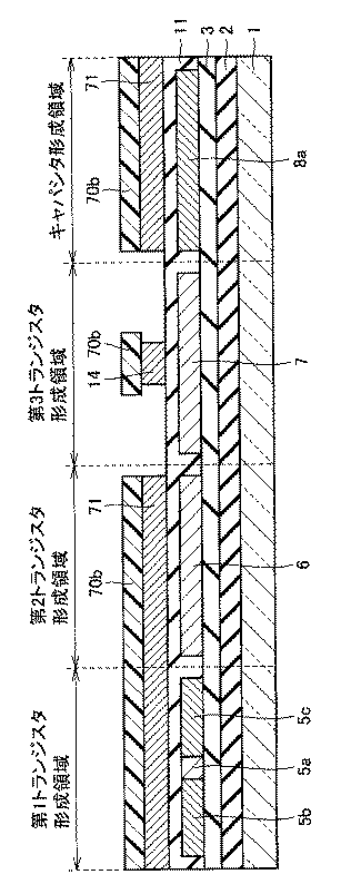
表1に示すように、LDD構造のTFTの耐圧が12.9Vであるのに対し、本発明のn型TFT30の耐圧は22.8Vとなっている。このことから、本発明のn型TFT30の耐圧はLDD構造のTFTの耐圧よりも高いことが分かる。また、LDD構造のTFTのオン電流が2.1×10⁻⁴Aであるのに対し、本発明のn型TFT30のオン電流は
2.2×10⁻⁴Aとなっている。このことから、本発明のn型TFT30のオン電流はLDD構造のTFTのオン電流とほぼ同様の値となっていることが分かる。
As shown in Table 1, the breakdown voltage of the LDD structure TFT is 12.9V, whereas the breakdown voltage of the n-
(実施例2)
本実施例においては、第1不純物領域5b,5cおよび下部電極8aの不純物濃度をそれぞれ5×10¹⁷原子/cm3,1×1018原子/cm3,2×1018原子/cm3と変化させて図1に示す実施の形態1の半導体装置100を製造した。そして、それぞれの半導体装置100についてキャパシタ60のフラットバンド電圧を測定した。この結果を表2に示す。なお、表2のフラットバンド電圧は、下部電極8aの電位に対する上部電極15の電位で示されている。
(Example 2)
In this embodiment, the impurity concentrations of the
表2に示すように、不純物濃度が5×10¹⁷原子/cm3である場合にはフラットバンド電圧は−2Vとなっており、不純物濃度が1×1017原子/cm3である場合にはフラットバンド電圧は−5Vとなっており、不純物濃度が2×1018原子/cm3である場合にはフラットバンド電圧は−10Vとなっている。ここで、フラットバンド電圧が−10Vである場合には、下部電極8aの電位を上部電極15の電位よりも−10V以上高くすることでキャパシタ60の容量が一定になる。表2の結果によれば、第1不純物領域5b,5cおよび下部電極8aの不純物濃度がいずれの場合にもフラットバンド電圧はマイナスとなっている。上述のように、フラットバンド電圧がマイナスであれば、下部電極8aの電位よりも上部電極15の電位を高く保つことによりキャパシタ60の容量は電圧に関わらず一定となる。したがって、本発明の半導体装置によれば、安定してキャパシタに電荷を蓄積することができ、画素電極の電圧の低下を十分に抑止できることがわかる。
As shown in Table 2, when the impurity concentration is 5 × 10 17 atoms / cm 3 , the flat band voltage is −2 V, and when the impurity concentration is 1 × 10 17 atoms / cm 3 The flat band voltage is −5V, and when the impurity concentration is 2 × 10 18 atoms / cm 3 , the flat band voltage is −10V. Here, when the flat band voltage is −10V, the capacitance of the
(実施例3)
本実施例においては、第1不純物領域5b,5cおよび下部電極8aの不純物濃度をそれぞれ5×10¹⁶原子/cm3、1×1017原子/cm3、5×1017原子/cm3と変化させて図1に示す実施の形態1の半導体装置100を製造した。そして、それぞれの半導体装置100のn型TFT30について、実施例1と同様の方法により耐圧を測定した。この結果を表3に示す。
(Example 3)
In this embodiment, the impurity concentrations of the
表3に示すように、不純物濃度が5×10¹⁶原子/cm3である場合にはn型TFT30の耐圧は14.2Vとなっており、不純物濃度が1×1017原子/cm3である場合にはn型TFT30の耐圧は23.5Vとなっており、不純物濃度が5×1017原子/cm3である場合にはn型TFT30の耐圧は22.8Vとなっている。実施例3と実施例2との結果から、不純物濃度を1×1017原子/cm3以上とすることにより、キャパシタ60のフラットバンド電圧がマイナスの値となり、かつn型TFT30の耐圧が一層向上することが分かる。
As shown in Table 3, when the impurity concentration is 5 × 10 16 atoms / cm 3 , the breakdown voltage of the n-
以上に開示された実施の形態および実施例はすべての点で例示であって制限的なものではないと考慮されるべきである。本発明の範囲は、以上の実施の形態および実施例ではなく、特許請求の範囲によって示され、特許請求の範囲と均等の意味および範囲内でのすべての修正や変形を含むものと意図される。 The embodiments and examples disclosed above are to be considered in all respects as illustrative and not restrictive. The scope of the present invention is shown not by the above embodiments and examples but by the scope of claims, and is intended to include all modifications and variations within the meaning and scope equivalent to the scope of claims. .
1 基板、2 SiN膜、3 下地膜、5〜8 多結晶シリコン膜、5a,6a,7a チャネル形成領域、5b〜5g,6b〜6e,8b〜8e 不純物領域、7b,30a,31a,40a ソース領域、7c,30b,31b,40b ドレイン領域、8a 下部電極、11 SiO2膜、12〜14 ゲート電極、15 上部電極、16,21 層間絶縁膜、16a〜16h 孔、17a〜17h コンタクト、19a,19c,19e ソース電極、19b,19d,19f ドレイン電極、19g,19h 配線、21a 溝、22 画素電極、30,31,40,41 n型TFT、50 p型TFT、60 キャパシタ、70a〜70d レジスト、71 導電膜、100,101 半導体装置。
1 substrate, 2 SiN film, 3 base film, 5-8 polycrystalline silicon film, 5a, 6a, 7a channel formation region, 5b-5g, 6b-6e, 8b-8e impurity region, 7b, 30a, 31a, 40a source Region, 7c, 30b, 31b, 40b drain region, 8a lower electrode, 11 SiO 2 film, 12-14 gate electrode, 15 upper electrode, 16, 21 interlayer insulating film, 16a-16h hole, 17a-17h contact, 19a, 19c, 19e source electrode, 19b, 19d, 19f drain electrode, 19g, 19h wiring, 21a groove, 22 pixel electrode, 30, 31, 40, 41 n-type TFT, 50 p-type TFT, 60 capacitor, 70a-70d resist, 71 Conductive film, 100, 101 Semiconductor device.
Claims (11)
前記トランジスタはソース領域およびドレイン領域を有し、
前記ソース領域および前記ドレイン領域の各々は、前記トランジスタのゲート電極の真下に形成された前記第1不純物領域と、前記第1不純物領域の不純物濃度よりも高い不純物濃度を有する第2不純物領域とを有し、
前記第1不純物領域の不純物濃度と前記キャパシタの一方電極の不純物濃度とが同じであることを特徴とする、半導体装置。 A semiconductor device comprising a transistor and a capacitor,
The transistor has a source region and a drain region;
Each of the source region and the drain region includes the first impurity region formed immediately below the gate electrode of the transistor and a second impurity region having an impurity concentration higher than that of the first impurity region. Have
The semiconductor device according to claim 1, wherein the impurity concentration of the first impurity region is the same as the impurity concentration of one electrode of the capacitor.
前記第3の不純物領域は前記第1不純物領域と前記第2不純物領域との間に形成されており、
前記第3不純物領域の不純物濃度は、前記第1不純物領域の不純物濃度よりも高く、前記第2の不純物領域の不純物濃度よりも低いことを特徴とする、請求項1に記載の半導体装置。 The transistor further includes a third impurity region,
The third impurity region is formed between the first impurity region and the second impurity region;
2. The semiconductor device according to claim 1, wherein an impurity concentration of the third impurity region is higher than an impurity concentration of the first impurity region and lower than an impurity concentration of the second impurity region.
第1トランジスタ形成領域とキャパシタ形成領域とを有する半導体膜を基板上に形成する工程と、
第1不純物濃度を有する1対の第1不純物領域を前記半導体膜の前記第1トランジスタ形成領域に形成する工程と、
前記1対の第1不純物領域の間に挟まれるチャネル形成領域と、前記1対の第1不純物領域の各々の一部とを第1絶縁膜を介して覆うように、前記第1トランジスタの第1ゲート電極を前記半導体膜上に形成する工程と、
前記第1不純物領域よりも不純物濃度の高い第2不純物濃度を有する1対の第2不純物領域を前記第1ゲート電極の真下を除く第1不純物領域内に形成する工程とを備え、
前記1対の第1不純物領域を形成する工程と同一の工程により、前記第1不純物濃度を有する前記キャパシタの一方電極が前記半導体膜に形成されることを特徴とする、半導体装置の製造方法。 A method of manufacturing a semiconductor device including a first transistor and a capacitor,
Forming a semiconductor film having a first transistor formation region and a capacitor formation region on a substrate;
Forming a pair of first impurity regions having a first impurity concentration in the first transistor formation region of the semiconductor film;
The first transistor includes a channel forming region sandwiched between the pair of first impurity regions and a part of each of the pair of first impurity regions via a first insulating film. Forming a gate electrode on the semiconductor film;
Forming a pair of second impurity regions having a second impurity concentration higher in impurity concentration than the first impurity region in the first impurity region except immediately below the first gate electrode;
A method of manufacturing a semiconductor device, wherein one electrode of the capacitor having the first impurity concentration is formed on the semiconductor film by the same step as the step of forming the pair of first impurity regions.
前記半導体膜の前記第1トランジスタ形成領域上に前記第1絶縁膜を介して第1導電膜を形成する工程と、
前記チャネル形成領域と、前記1対の第1不純物領域の各々の一部とを覆うように、第1レジストを前記第1導電膜上に形成する工程と、
前記第1レジストをマスクとして、前記第1レジストよりも線幅が細くなるように前記第1導電膜をエッチングする工程とを含み、
前記第1レジストをマスクとして不純物を注入することにより前記第2不純物濃度を有する前記1対の第2不純物領域が前記第1不純物領域内に形成され、
前記第1のゲート電極をマスクとして不純物を注入することにより前記1対の第3不純物領域が形成されることを特徴とする、請求項8に記載の半導体装置の製造方法。 The step of forming the first gate electrode includes:
Forming a first conductive film on the first transistor formation region of the semiconductor film via the first insulating film;
Forming a first resist on the first conductive film so as to cover the channel formation region and a part of each of the pair of first impurity regions;
Etching the first conductive film so that the line width is narrower than that of the first resist, using the first resist as a mask,
The pair of second impurity regions having the second impurity concentration are formed in the first impurity regions by implanting impurities using the first resist as a mask,
9. The method of manufacturing a semiconductor device according to claim 8, wherein the pair of third impurity regions are formed by implanting impurities using the first gate electrode as a mask.
前記第2トランジスタを形成する工程は、
前記第1導電膜を形成する工程と同一の工程により、前記第2トランジスタ形成領域をさらに有する前記半導体膜の前記第2トランジスタ形成領域上に第2絶縁膜を介して第2導電膜を形成する工程と、
第1レジストを形成する工程と同一の工程により、第2レジストを前記第2導電膜上に形成する工程と、
前記第1導電膜をエッチングする工程と同一の工程により、前記第2レジストをマスクとして、前記第2レジストよりも線幅が細くなるように前記第2導電膜をエッチングする工程と、
前記1対の第2不純物領域を形成する工程と同一の工程により、前記第2レジストをマスクとして不純物を注入することにより第4不純物濃度を有する1対の第4不純物領域を前記半導体層の前記第2トランジスタ形成領域に形成する工程と、
前記1対の第3不純物領域を形成する工程と同一の工程により、前記第2導電層をマスクとして不純物を注入することにより第5の不純物濃度を有する1対の第5不純物領域を形成する工程とを含むことを特徴とする、請求項9に記載の半導体装置の製造方法。 A step of forming a second transistor;
The step of forming the second transistor includes:
A second conductive film is formed on the second transistor formation region of the semiconductor film further having the second transistor formation region through a second insulating film by the same step as the step of forming the first conductive film. Process,
A step of forming a second resist on the second conductive film by the same step as the step of forming the first resist;
Etching the second conductive film so that the line width is narrower than that of the second resist by using the second resist as a mask in the same step as the step of etching the first conductive film;
In the same step as the step of forming the pair of second impurity regions, a pair of fourth impurity regions having a fourth impurity concentration is implanted into the semiconductor layer by implanting impurities using the second resist as a mask. Forming in the second transistor formation region;
A step of forming a pair of fifth impurity regions having a fifth impurity concentration by implanting impurities using the second conductive layer as a mask in the same step as the step of forming the pair of third impurity regions. The method for manufacturing a semiconductor device according to claim 9, comprising:
11. The method of manufacturing a semiconductor device according to claim 7, wherein the other electrode of the capacitor is formed by the same step as the step of forming the first gate electrode.
Priority Applications (1)
| Application Number | Priority Date | Filing Date | Title |
|---|---|---|---|
| JP2004105182A JP2005294418A (en) | 2004-03-31 | 2004-03-31 | Semiconductor device and manufacturing method thereof |
Applications Claiming Priority (1)
| Application Number | Priority Date | Filing Date | Title |
|---|---|---|---|
| JP2004105182A JP2005294418A (en) | 2004-03-31 | 2004-03-31 | Semiconductor device and manufacturing method thereof |
Publications (1)
| Publication Number | Publication Date |
|---|---|
| JP2005294418A true JP2005294418A (en) | 2005-10-20 |
Family
ID=35327036
Family Applications (1)
| Application Number | Title | Priority Date | Filing Date |
|---|---|---|---|
| JP2004105182A Pending JP2005294418A (en) | 2004-03-31 | 2004-03-31 | Semiconductor device and manufacturing method thereof |
Country Status (1)
| Country | Link |
|---|---|
| JP (1) | JP2005294418A (en) |
Cited By (1)
| Publication number | Priority date | Publication date | Assignee | Title |
|---|---|---|---|---|
| JP2008015454A (en) * | 2006-06-30 | 2008-01-24 | Lg Phillips Lcd Co Ltd | Liquid crystal display device and manufacturing method thereof |
Citations (3)
| Publication number | Priority date | Publication date | Assignee | Title |
|---|---|---|---|---|
| JP2001024196A (en) * | 1999-07-05 | 2001-01-26 | Semiconductor Energy Lab Co Ltd | Manufacturing method of electro-optical device |
| JP2002006340A (en) * | 2000-06-26 | 2002-01-09 | Seiko Epson Corp | Liquid crystal device, method of manufacturing the same, and electronic equipment |
| JP2003149675A (en) * | 2001-11-15 | 2003-05-21 | Hitachi Ltd | Liquid crystal display |
-
2004
- 2004-03-31 JP JP2004105182A patent/JP2005294418A/en active Pending
Patent Citations (3)
| Publication number | Priority date | Publication date | Assignee | Title |
|---|---|---|---|---|
| JP2001024196A (en) * | 1999-07-05 | 2001-01-26 | Semiconductor Energy Lab Co Ltd | Manufacturing method of electro-optical device |
| JP2002006340A (en) * | 2000-06-26 | 2002-01-09 | Seiko Epson Corp | Liquid crystal device, method of manufacturing the same, and electronic equipment |
| JP2003149675A (en) * | 2001-11-15 | 2003-05-21 | Hitachi Ltd | Liquid crystal display |
Cited By (4)
| Publication number | Priority date | Publication date | Assignee | Title |
|---|---|---|---|---|
| JP2008015454A (en) * | 2006-06-30 | 2008-01-24 | Lg Phillips Lcd Co Ltd | Liquid crystal display device and manufacturing method thereof |
| US8269907B2 (en) | 2006-06-30 | 2012-09-18 | Lg Display Co., Ltd. | Liquid crystal display device and method for fabricating the same |
| KR101250789B1 (en) * | 2006-06-30 | 2013-04-08 | 엘지디스플레이 주식회사 | Method of fabricating liquid crystal display device |
| US8665386B2 (en) | 2006-06-30 | 2014-03-04 | Lg Display Co., Ltd. | Liquid crystal display device and method for fabricating the same |
Similar Documents
| Publication | Publication Date | Title |
|---|---|---|
| JP2666103B2 (en) | Thin film semiconductor device | |
| US10468533B2 (en) | Semiconductor device and method for manufacturing same | |
| CN101924111B (en) | Semiconductor device and method of manufacturing the same | |
| US7700995B2 (en) | Semiconductor device and display device | |
| JP2009290211A (en) | Semiconductor device and method of manufacturing the same | |
| CN1909249B (en) | Semiconductor device with thin film transistor and manufacturing method thereof | |
| CN100495730C (en) | Semiconductor device and image display apparatus | |
| JP3296975B2 (en) | Thin film transistor and method of manufacturing the same | |
| JPH10256554A (en) | Thin film transistor and method of manufacturing the same | |
| JP2005228819A (en) | Semiconductor device | |
| US8513766B2 (en) | Semiconductor device having a drain-gate isolation portion | |
| JP2004040108A (en) | Thin film transistor having LDD structure and method of manufacturing the same | |
| JP2005311037A (en) | Semiconductor device and manufacturing method thereof | |
| JP2005333107A (en) | Semiconductor device, image display device, and method of manufacturing semiconductor device | |
| JPH098314A (en) | Thin film transistor | |
| JPH05275701A (en) | Thin film transistor | |
| US20100207120A1 (en) | Production method of semiconductor device and semiconductor device | |
| CN100505310C (en) | Semiconductor device and image display device | |
| JP2005294418A (en) | Semiconductor device and manufacturing method thereof | |
| TW200417035A (en) | TFT structure with LDD region and manufacturing process of the same | |
| JP5414712B2 (en) | Semiconductor device | |
| JP3398665B2 (en) | Method for manufacturing thin film transistor | |
| JP4342191B2 (en) | Device having thin film transistor and method for manufacturing the same | |
| US8124979B2 (en) | Thin film transistor and method of manufacturing the same | |
| KR101385471B1 (en) | Thin film transistor and method for fabricating the same, liquid crystal display device and organic light emitting diode display device using the same |
Legal Events
| Date | Code | Title | Description |
|---|---|---|---|
| A621 | Written request for application examination |
Free format text: JAPANESE INTERMEDIATE CODE: A621 Effective date: 20061005 |
|
| A977 | Report on retrieval |
Free format text: JAPANESE INTERMEDIATE CODE: A971007 Effective date: 20090903 |
|
| A131 | Notification of reasons for refusal |
Free format text: JAPANESE INTERMEDIATE CODE: A131 Effective date: 20090908 |
|
| A521 | Written amendment |
Free format text: JAPANESE INTERMEDIATE CODE: A523 Effective date: 20091106 |
|
| A02 | Decision of refusal |
Free format text: JAPANESE INTERMEDIATE CODE: A02 Effective date: 20100330 |