JP2005294250A - Light emitting element - Google Patents
Light emitting element Download PDFInfo
- Publication number
- JP2005294250A JP2005294250A JP2005021268A JP2005021268A JP2005294250A JP 2005294250 A JP2005294250 A JP 2005294250A JP 2005021268 A JP2005021268 A JP 2005021268A JP 2005021268 A JP2005021268 A JP 2005021268A JP 2005294250 A JP2005294250 A JP 2005294250A
- Authority
- JP
- Japan
- Prior art keywords
- light emitting
- light
- layer
- organic compound
- emitting element
- Prior art date
- Legal status (The legal status is an assumption and is not a legal conclusion. Google has not performed a legal analysis and makes no representation as to the accuracy of the status listed.)
- Granted
Links
- 0 *c(cc1)ccc1-c1ccc(C(c(cc2)ccc2-c2ccc(*)cc2)(c(cc2)ccc2-c2ccc(*)cc2)c(cc2)ccc2-c2ccc(*)cc2)cc1 Chemical compound *c(cc1)ccc1-c1ccc(C(c(cc2)ccc2-c2ccc(*)cc2)(c(cc2)ccc2-c2ccc(*)cc2)c(cc2)ccc2-c2ccc(*)cc2)cc1 0.000 description 2
Classifications
-
- H—ELECTRICITY
- H10—SEMICONDUCTOR DEVICES; ELECTRIC SOLID-STATE DEVICES NOT OTHERWISE PROVIDED FOR
- H10K—ORGANIC ELECTRIC SOLID-STATE DEVICES
- H10K50/00—Organic light-emitting devices
- H10K50/10—OLEDs or polymer light-emitting diodes [PLED]
- H10K50/11—OLEDs or polymer light-emitting diodes [PLED] characterised by the electroluminescent [EL] layers
- H10K50/12—OLEDs or polymer light-emitting diodes [PLED] characterised by the electroluminescent [EL] layers comprising dopants
-
- H—ELECTRICITY
- H10—SEMICONDUCTOR DEVICES; ELECTRIC SOLID-STATE DEVICES NOT OTHERWISE PROVIDED FOR
- H10K—ORGANIC ELECTRIC SOLID-STATE DEVICES
- H10K50/00—Organic light-emitting devices
- H10K50/10—OLEDs or polymer light-emitting diodes [PLED]
- H10K50/11—OLEDs or polymer light-emitting diodes [PLED] characterised by the electroluminescent [EL] layers
-
- H—ELECTRICITY
- H10—SEMICONDUCTOR DEVICES; ELECTRIC SOLID-STATE DEVICES NOT OTHERWISE PROVIDED FOR
- H10K—ORGANIC ELECTRIC SOLID-STATE DEVICES
- H10K2101/00—Properties of the organic materials covered by group H10K85/00
- H10K2101/10—Triplet emission
-
- H—ELECTRICITY
- H10—SEMICONDUCTOR DEVICES; ELECTRIC SOLID-STATE DEVICES NOT OTHERWISE PROVIDED FOR
- H10K—ORGANIC ELECTRIC SOLID-STATE DEVICES
- H10K85/00—Organic materials used in the body or electrodes of devices covered by this subclass
- H10K85/30—Coordination compounds
- H10K85/321—Metal complexes comprising a group IIIA element, e.g. Tris (8-hydroxyquinoline) gallium [Gaq3]
- H10K85/324—Metal complexes comprising a group IIIA element, e.g. Tris (8-hydroxyquinoline) gallium [Gaq3] comprising aluminium, e.g. Alq3
-
- H—ELECTRICITY
- H10—SEMICONDUCTOR DEVICES; ELECTRIC SOLID-STATE DEVICES NOT OTHERWISE PROVIDED FOR
- H10K—ORGANIC ELECTRIC SOLID-STATE DEVICES
- H10K85/00—Organic materials used in the body or electrodes of devices covered by this subclass
- H10K85/30—Coordination compounds
- H10K85/341—Transition metal complexes, e.g. Ru(II)polypyridine complexes
- H10K85/342—Transition metal complexes, e.g. Ru(II)polypyridine complexes comprising iridium
-
- Y—GENERAL TAGGING OF NEW TECHNOLOGICAL DEVELOPMENTS; GENERAL TAGGING OF CROSS-SECTIONAL TECHNOLOGIES SPANNING OVER SEVERAL SECTIONS OF THE IPC; TECHNICAL SUBJECTS COVERED BY FORMER USPC CROSS-REFERENCE ART COLLECTIONS [XRACs] AND DIGESTS
- Y10—TECHNICAL SUBJECTS COVERED BY FORMER USPC
- Y10S—TECHNICAL SUBJECTS COVERED BY FORMER USPC CROSS-REFERENCE ART COLLECTIONS [XRACs] AND DIGESTS
- Y10S428/00—Stock material or miscellaneous articles
- Y10S428/917—Electroluminescent
Abstract
Description
本発明は、耐久性が極めて優れ、かつ発光輝度、発光効率が極めて高い発光素子に関し、特に有機電界発光素子として好適な発光素子に関する。 The present invention relates to a light-emitting element that is extremely excellent in durability and has extremely high light emission luminance and light emission efficiency, and particularly relates to a light-emitting element suitable as an organic electroluminescent element.
有機物質を使用した有機発光素子は、固体発光型の安価な大面積フルカラー表示素子や書き込み光源アレイとしての用途が有望視され、多くの開発が行われている。一般に有機発光素子は、発光層及び該層を挟んだ一対の対向電極から構成されている。両電極間に電界が印加されると、陰極から電子が注入され、陽極から正孔が注入される。発光は、この電子と正孔が発光層において再結合し、エネルギー準位が伝導帯から価電子帯に戻る際にエネルギーを光として放出する現象である。 Organic light-emitting devices using organic substances are promising for use as solid light-emitting, inexpensive large-area full-color display devices and writing light source arrays, and many developments have been made. In general, an organic light emitting device is composed of a light emitting layer and a pair of counter electrodes sandwiching the layer. When an electric field is applied between both electrodes, electrons are injected from the cathode and holes are injected from the anode. Light emission is a phenomenon in which energy is released as light when the electrons and holes recombine in the light emitting layer and the energy level returns from the conduction band to the valence band.
しかしながら、このような有機発光素子の場合、無機LED素子や、蛍光管に比べ非常に発光効率が低いという大きな問題がある。
現在提案されている有機発光素子の殆どは、有機発光材料の一重項励起子から得られる蛍光発光を利用したものである。単純な量子化学のメカニズムにおいては、励起子状態において、蛍光発光が得られる一重項励起子と、燐光発光が得られる三重項励起子との比は、1対3であり、蛍光発光を利用している限りは励起子の25%しか有効活用できず発光効率は低いものとなる。
それに対して三重項励起子から得られる燐光を利用できるようになれば、発光効率を向上でき、実際に、近年、イリジウムのフェニルピリジン錯体を用いた燐光利用の有機発光素子が報告され、従来の蛍光利用の有機発光素子に対して、2〜3倍の発光効率を示す旨が報告されている(例えば、特許文献1、非特許文献1、非特許文献2参照)。
However, in the case of such an organic light emitting device, there is a big problem that the light emission efficiency is very low as compared with inorganic LED devices and fluorescent tubes.
Most of the organic light-emitting devices that are currently proposed utilize fluorescence emitted from singlet excitons of organic light-emitting materials. In the mechanism of simple quantum chemistry, in the exciton state, the ratio of singlet excitons that give fluorescence emission to triplet excitons that give phosphorescence emission is 1 to 3, and it uses fluorescence emission. As long as it is, only 25% of the excitons can be effectively used, and the luminous efficiency is low.
On the other hand, if the phosphorescence obtained from triplet excitons can be used, the luminous efficiency can be improved. In recent years, phosphorescent organic light emitting devices using iridium phenylpyridine complexes have been reported, It has been reported that the fluorescent light-emitting organic light-emitting element exhibits a light emission efficiency of 2 to 3 times (see, for example, Patent Document 1, Non-Patent Document 1, and Non-Patent Document 2).
燐光利用の有機発光素子の多くは、陽極/正孔輸送層/発光層/ブロック層/電子輸送層/陰極の素子構成を有する。発光層には、主として、発光材料に三重項励起子エネルギーをエネルギー移動させるホスト材料と燐光発光材料とが用いられており、ホスト材料としては一般にCBP(4,4'−N,N''−ジカルバゾールビフェニル)等のカルバゾール化合物がよく用いられる。
ホスト材料から燐光発光材料へ三重項励起子エネルギーを効率よく移動させるためには、ホスト材料の三重項最低励起準位T1が発光材料のそれよりも大きくする必要がある。
緑発光材料や、赤発光材料では、CBPをホスト材料に用いても、発光材料よりCBPの方がT1は十分に大きくなるので、高い発光効率が得られる。
しかしながら、青発光材料の場合、発光材料のT1がホスト材料であるCBPのT1より大きくなるため、三重項励起子エネルギーを効率よく移動させることが困難となり発光効率が大幅に低下することが大きな問題となっている。
Many of the organic light emitting devices utilizing phosphorescence have an element configuration of anode / hole transport layer / light emitting layer / block layer / electron transport layer / cathode. In the light emitting layer, a host material and a phosphorescent material that transfer triplet exciton energy to the light emitting material are mainly used. As the host material, CBP (4,4′-N, N ″ − is generally used. Carbazole compounds such as dicarbazole biphenyl) are often used.
In order to efficiently transfer the triplet exciton energy from the host material to the phosphorescent material, it is necessary to make the triplet lowest excited level T1 of the host material larger than that of the light emitting material.
In the green light emitting material and the red light emitting material, even if CBP is used as the host material, CBP is sufficiently larger than the light emitting material, so that high luminous efficiency can be obtained.
However, in the case of a blue light emitting material, since T1 of the light emitting material is larger than T1 of CBP as the host material, it is difficult to efficiently move triplet exciton energy, and the luminous efficiency is greatly reduced. It has become.
青発光材料用のT1の大きなホスト材料として、CBPのビフェニルにメチル基を入れたCDBP(4,4'−ビス(9−カルバゾリル)−2,2'−ジメチル−ビフェニル)が報告されている(例えば、非特許文献3参照)。しかしながら、その発光効率はまだまだ低く、また耐久性にも問題があるものである CDBP (4,4′-bis (9-carbazolyl) -2,2′-dimethyl-biphenyl) in which a methyl group is added to biphenyl of CBP has been reported as a host material having a large T1 for a blue light emitting material ( For example, refer nonpatent literature 3). However, its luminous efficiency is still low and there is a problem with durability.
一方、発光層において、ホスト材料を含まず、発光材料のみで発光させることも可能であるが、発光材料同士の相互作用により消光し、発光輝度および発光効率が共に低くなるという問題がある。
それを解決する目的で、発光層中に電気的に不活性な無機誘電体と発光材料を共存させる方法が提案されている(例えば、特許文献2参照)。しかしながら、乾式製膜法で無機誘電体と発光材料である有機化合物とを共製膜して発光層を形成するためには、用いることのできる発光材料が制約される。
また、発光層に電気的に不活性なポリマーバインダーを用いる方法も開示されている(例えば、特許文献3参照)。しかしながら、ポリマーを用いるために発光素子の製法が湿式製膜法に限られる(特許文献3参照)。
In order to solve this problem, a method has been proposed in which an electrically inactive inorganic dielectric and a light emitting material coexist in the light emitting layer (see, for example, Patent Document 2). However, in order to form a light emitting layer by co-depositing an inorganic dielectric and an organic compound as a light emitting material by a dry film forming method, the light emitting material that can be used is limited.
Further, a method using an electrically inactive polymer binder for the light emitting layer is also disclosed (for example, see Patent Document 3). However, since a polymer is used, a method for manufacturing a light-emitting element is limited to a wet film forming method (see Patent Document 3).
発光素子においては発光効率や発光輝度が高いことが要求され、以上のとおり、燐光発光を利用する発光素子においては、青発光、緑発光、赤発光のいずれにおいても発光効率や発光輝度が高く、しかも耐久性が優れた素子が強く望まれているのが現状である。
本発明は、このような事情に鑑み、耐久性に優れ、発光効率および発光輝度の高い発光素子を提供することを目的とする。
The light emitting element is required to have high luminous efficiency and luminance, and as described above, in the light emitting element utilizing phosphorescence, the luminous efficiency and luminance are high in any of blue light emission, green light emission, and red light emission, In addition, there is a strong demand for devices with excellent durability.
In view of such circumstances, an object of the present invention is to provide a light-emitting element that has excellent durability and high light emission efficiency and light emission luminance.
本発明よれば、下記の発光素子が提供され、本発明の上記目的が達成される。
<1>一対の電極間に、少なくとも一層の発光層を含む有機化合物層を有する発光素子であって、
該発光層が、発光材料と、乾式製膜可能で、最高占有軌道と最低非占有軌道とのエネルギー差Egが4.0eV以上である電気的に不活性な有機化合物とを含むことを特徴とする発光素子。
<2>発光材料として燐光発光材料を含むことを特徴とする上記<1>に記載の発光素子。
<3>前記電気的に不活性な有機化合物の三重項最低励起準位T1が、2.7eV以上であることを特徴とする上記<1>または<2>に記載の発光素子。
<4>前記電気的に不活性な有機化合物のイオン化ポテンシャルIpが、6.1eV以上であることを特徴とする上記<1>〜<3>のいずれかに記載の発光素子。
<5>前記電気的に不活性な有機化合物が、芳香族炭化水素化合物であることを特徴とする上記<1>〜<4>のいずれかに記載の発光素子。
<6>前記電気的に不活性な有機化合物が、下記一般式(1)で示される化合物であることを特徴とする上記<1>〜<5>のいずれかに記載の発光素子。
According to the present invention, the following light emitting device is provided, and the above object of the present invention is achieved.
<1> A light emitting device having an organic compound layer including at least one light emitting layer between a pair of electrodes,
The light-emitting layer includes a light-emitting material and an electrically inactive organic compound that can be formed into a dry film and has an energy difference Eg of 4.0 eV or more between the highest occupied orbital and the lowest unoccupied orbital. Light emitting element.
<2> The light-emitting element according to <1>, wherein the light-emitting material includes a phosphorescent material.
<3> The light-emitting element according to <1> or <2>, wherein the triplet lowest excitation level T1 of the electrically inactive organic compound is 2.7 eV or more.
<4> The light-emitting element according to any one of <1> to <3>, wherein an ionization potential Ip of the electrically inactive organic compound is 6.1 eV or more.
<5> The light emitting device according to any one of <1> to <4>, wherein the electrically inactive organic compound is an aromatic hydrocarbon compound.
<6> The light emitting device according to any one of <1> to <5>, wherein the electrically inactive organic compound is a compound represented by the following general formula (1).
一般式(1) L−(Ar)m General formula (1) L- (Ar) m
一般式(1)中、Arは下記一般式(2)で表される基、Lは3価以上のベンゼン骨格を表し、mは3以上の整数を表す。 In general formula (1), Ar represents a group represented by the following general formula (2), L represents a trivalent or higher benzene skeleton, and m represents an integer of 3 or higher.
一般式(2)中、R1は置換基を表し、R1が複数存在する場合、互いに同じでも異なっていてもよい。n1は0〜9の整数を表す。 In general formula (2), R 1 represents a substituent, and when a plurality of R 1 are present, they may be the same as or different from each other. n1 represents an integer of 0 to 9.
<7>前記電気的に不活性な有機化合物が、下記一般式(3)で示される化合物であることを特徴とする上記<1>〜<5>のいずれかに記載の発光素子。 <7> The light-emitting element according to any one of <1> to <5>, wherein the electrically inactive organic compound is a compound represented by the following general formula (3).
一般式(3)中、R2は置換基を表し、R2が複数存在する場合、互いに同じでも異なっていてもよい。n2は0〜20の整数を表す。 In General Formula (3), R 2 represents a substituent, and when a plurality of R 2 are present, they may be the same as or different from each other. n2 represents an integer of 0-20.
本発明の発光素子は、以上の構成のように、発光層に発光材料と、最高占有軌道と最低非占有軌道とのエネルギー差Egが4.0eV以上の電気的に不活性な有機化合物とを用いることにより、ホスト材料を使うことなく高輝度、高効率で燐光発光させることができる。その結果、本発明の発光素子は、発光輝度、発光効率が高く、耐久性にも優れる。
本発明の発光素子は、フルカラーディスプレイ、バックライト等の面光源やプリンター等の光源アレイなどに有効に利用できる。
In the light emitting device of the present invention, as described above, the light emitting layer includes a light emitting material and an electrically inactive organic compound having an energy difference Eg of 4.0 eV or more between the highest occupied orbital and the lowest unoccupied orbital. By using it, phosphorescence can be emitted with high luminance and high efficiency without using a host material. As a result, the light-emitting element of the present invention has high light emission luminance and light emission efficiency, and is excellent in durability.
The light emitting device of the present invention can be effectively used for a surface light source such as a full color display and a backlight, a light source array such as a printer, and the like.
本発明の発光素子は、一対の電極間に、少なくとも一層の発光層を含む有機化合物層を有する発光素子であり、該発光層に、発光材料と、乾式製膜可能で、最高占有軌道と最低非占有軌道とのエネルギー差Egが4.0eV以上である電気的に不活性な有機化合物とを含む発光素子である。
このように、発光層に発光材料と、最高占有軌道と最低非占有軌道とのエネルギー差Egが4.0eV以上の電気的に不活性な有機化合物とを用いることにより、発光層にホスト材料を含まなくとも発光材料に直接励起子を生成することが可能となる。また、発光材料が前記電気的に不活性な有機化合物間に分子分散されることになるため、発光材料間の相互作用もなく消光することもない。その結果、ホスト材料を使うことなく高効率で燐光発光させることができ、非常に発光効率の高い発光素子を得ることができる。
The light-emitting element of the present invention is a light-emitting element having an organic compound layer including at least one light-emitting layer between a pair of electrodes, and a light-emitting material and a dry film can be formed on the light-emitting layer. It is a light emitting element including an electrically inactive organic compound having an energy difference Eg with respect to an unoccupied orbital of 4.0 eV or more.
Thus, by using a light emitting material for the light emitting layer and an electrically inactive organic compound having an energy difference Eg between the highest occupied orbital and the lowest unoccupied orbit of 4.0 eV or more, the host material is added to the light emitting layer. Even if it is not included, excitons can be directly generated in the light emitting material. Further, since the light emitting material is molecularly dispersed between the electrically inactive organic compounds, there is no interaction between the light emitting materials and no quenching occurs. As a result, phosphorescence can be emitted with high efficiency without using a host material, and a light-emitting element with extremely high emission efficiency can be obtained.
本発明では、前記電気的に不活性な有機化合物は、発光層内で乾式製膜可能な良好なバインダー材料として作用している。
最高占有軌道と最低非占有軌道とのエネルギー差Egが4.0eV以上、すなわち電気的に不活性なので、発光材料の希釈効果を大きくすることができ、発光効率や耐久性が改良される。
乾式製膜可能な材料とは、蒸着法等の乾式製膜法により分解することなく製膜できる材料のことであり、分子量は300以上2000以下が好ましい。
In the present invention, the electrically inactive organic compound acts as a good binder material capable of dry film formation in the light emitting layer.
Since the energy difference Eg between the highest occupied track and the lowest unoccupied track is 4.0 eV or more, that is, electrically inactive, the dilution effect of the light emitting material can be increased, and the light emission efficiency and durability are improved.
The dry film forming material is a material that can be formed without being decomposed by a dry film forming method such as an evaporation method, and the molecular weight is preferably 300 or more and 2000 or less.
本発明においては、発光効率の点から、発光層に燐光発光材料を用いることが好ましい。
また、前記電気的に不活性な有機化合物の三重項最低励起準位T1は2.7eV以上であることが好ましい。このようにすると、該電気的に不活性な有機化合物への発光材料からの励起子拡散が抑制され、発光効率を一層向上させることができる点で好ましい。さらにT1は2.8eV以上がより好ましい。特に、発光材料が燐光青発光材料の場合、そのT1は2.6eV前後であり、これからの三重項励起子拡散抑制のためには、電気的に不活性な有機化合物のT1はそれ以上、すなわち2.7eV以上であることが好ましく、このようにすることにより燐光青発光素子においても、発光効率を一層向上させることができる。
In the present invention, it is preferable to use a phosphorescent material for the light emitting layer from the viewpoint of luminous efficiency.
The triplet lowest excitation level T1 of the electrically inactive organic compound is preferably 2.7 eV or more. This is preferable in that the exciton diffusion from the light emitting material to the electrically inactive organic compound is suppressed and the light emission efficiency can be further improved. Furthermore, T1 is more preferably 2.8 eV or more. In particular, when the light-emitting material is a phosphorescent blue light-emitting material, its T1 is around 2.6 eV, and in order to suppress triplet exciton diffusion from now on, T1 of an electrically inactive organic compound is more than that, that is, It is preferable that it is 2.7 eV or more, and by doing so, the luminous efficiency can be further improved in the phosphorescent blue light emitting device.
さらに本発明においては、電気的に不活性な有機化合物のイオン化ポテンシャルIpは6.1eV以上であることが好ましい。このようにすると、該電気的に不活性な有機化合物への発光材料からの正孔の移動が抑制され、発光材料に正孔が留まり、励起子の生成確率を向上させることができ、その結果、発光効率を一層向上させることができる点で好ましい。さらにIpは6.2eV以上がより好ましく、6.3eV以上が特に好ましい。特に、発光材料が燐光青発光材料の場合、そのイオン化ポテンシャルは5.8〜5.9eVであり、この燐光青発光材料から電気的に不活性な有機化合物へ正孔を移動させないためには、電気的に不活性な有機化合物のイオン化ポテンシャルはそれ以上、すなわち6.0eV以上であることが好ましく、このようにすることにより、燐光青発光素子においても、発光効率を一層向上させることができる。 Furthermore, in the present invention, the ionization potential Ip of the electrically inactive organic compound is preferably 6.1 eV or more. In this way, the movement of holes from the luminescent material to the electrically inactive organic compound is suppressed, holes can remain in the luminescent material, and the exciton generation probability can be improved. This is preferable in that the luminous efficiency can be further improved. Further, Ip is more preferably 6.2 eV or more, and particularly preferably 6.3 eV or more. In particular, when the light emitting material is a phosphorescent blue light emitting material, its ionization potential is 5.8 to 5.9 eV, and in order not to move holes from this phosphorescent blue light emitting material to an electrically inactive organic compound, The ionization potential of the electrically inactive organic compound is preferably more than that, that is, 6.0 eV or more. By doing so, the luminous efficiency can be further improved in the phosphorescent blue light-emitting device.
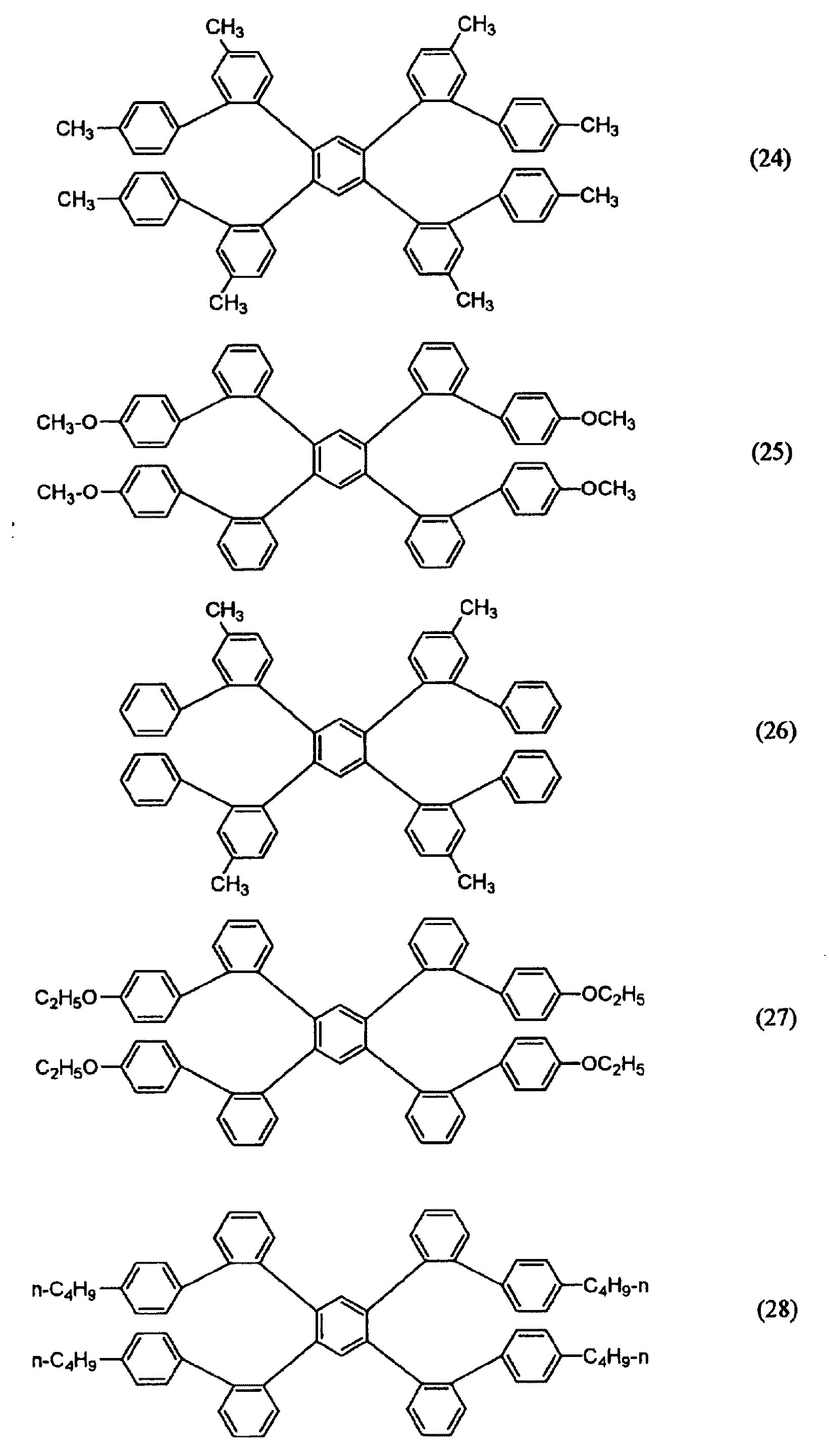
本発明においては、電気的に不活性な有機化合物は上記条件を満足する化合物であれば特に限定されることはないが、安定性の観点から、芳香族炭化水素が好ましく、下記一般式(1)または一般式(3)で表される化合物がより好ましい。 In the present invention, the electrically inactive organic compound is not particularly limited as long as it satisfies the above conditions, but from the viewpoint of stability, an aromatic hydrocarbon is preferable, and the following general formula (1) ) Or a compound represented by the general formula (3) is more preferable.
一般式(1) L−(Ar)m General formula (1) L- (Ar) m
一般式(1)中、Arは下記一般式(2)で表される基、Lは3価以上のベンゼン骨格を表し、mは3以上の整数を表す。 In general formula (1), Ar represents a group represented by the following general formula (2), L represents a trivalent or higher benzene skeleton, and m represents an integer of 3 or higher.
一般式(2)中、R1は置換基を表し、R1が複数存在する場合、互いに同じでも異なっていてもよい。n1は0〜9の整数を表す。 In general formula (2), R 1 represents a substituent, and when a plurality of R 1 are present, they may be the same as or different from each other. n1 represents an integer of 0 to 9.
一般式(3)中、R2は置換基を表し、R2が複数存在する場合、互いに同じでも異なっていてもよい。n2は0〜20の整数を表す。 In General Formula (3), R 2 represents a substituent, and when a plurality of R 2 are present, they may be the same as or different from each other. n2 represents an integer of 0-20.
まず、一般式(1)について詳細に説明する。
一般式(1)に含まれるLは3価以上のベンゼン骨格を表す。Arは一般式(2)で表される基を表し、mは3以上の整数を表す。mは好ましくは3以上6以下であり、さらに好ましくは3または4である。
First, the general formula (1) will be described in detail.
L contained in the general formula (1) represents a trivalent or higher benzene skeleton. Ar represents a group represented by the general formula (2), and m represents an integer of 3 or more. m is preferably 3 or more and 6 or less, and more preferably 3 or 4.
次に、一般式(2)で表される基について説明する。
一般式(2)に含まれるR1は置換基を表す。ここで置換基としては、例えば、アルキル基(好ましくは炭素数1〜30、より好ましくは炭素数1〜20、特に好ましくは炭素数1〜10であり、例えばメチル、エチル、iso−プロピル、tert−ブチル、n−オクチル、n−デシル、n−ヘキサデシル、シクロプロピル、シクロペンチル、シクロヘキシルなどが挙げられる)、アルケニル基(好ましくは炭素数2〜30、より好ましくは炭素数2〜20、特に好ましくは炭素数2〜10であり、例えばビニル、アリル、2−ブテニル、3−ペンテニルなどが挙げられる)、アルキニル基(好ましくは炭素数2〜30、より好ましくは炭素数2〜20、特に好ましくは炭素数2〜10であり、例えばプロパルギル、3−ペンチニルなどが挙げられる)、アリール基(好ましくは炭素数6〜30、より好ましくは炭素数6〜20、特に好ましくは炭素数6〜12であり、例えばフェニル、p−メチルフェニル、ナフチル、アントラニルなどが挙げられる)、
Next, the group represented by the general formula (2) will be described.
R 1 contained in the general formula (2) represents a substituent. Here, examples of the substituent include an alkyl group (preferably having 1 to 30 carbon atoms, more preferably 1 to 20 carbon atoms, and particularly preferably 1 to 10 carbon atoms such as methyl, ethyl, iso-propyl, tert. -Butyl, n-octyl, n-decyl, n-hexadecyl, cyclopropyl, cyclopentyl, cyclohexyl, etc.), an alkenyl group (preferably having 2 to 30 carbon atoms, more preferably 2 to 20 carbon atoms, particularly preferably 2 to 10 carbon atoms such as vinyl, allyl, 2-butenyl, 3-pentenyl, etc.), alkynyl groups (preferably having 2 to 30 carbon atoms, more preferably 2 to 20 carbon atoms, particularly preferably carbon atoms). 2 to 10, for example, propargyl, 3-pentynyl, etc.), aryl group (preferably carbon number) 30, more preferably 6 to 20 carbon atoms, particularly preferably 6 to 12 carbon atoms, such as phenyl, p- methylphenyl, naphthyl, anthranyl),
アミノ基(好ましくは炭素数0〜30、より好ましくは炭素数0〜20、特に好ましくは炭素数0〜10であり、例えばアミノ、メチルアミノ、ジメチルアミノ、ジエチルアミノ、ジベンジルアミノ、ジフェニルアミノ、ジトリルアミノなどが挙げられる)、アルコキシ基(好ましくは炭素数1〜30、より好ましくは炭素数1〜20、特に好ましくは炭素数1〜10であり、例えばメトキシ、エトキシ、ブトキシ、2−エチルヘキシロキシなどが挙げられる)、アリールオキシ基(好ましくは炭素数6〜30、より好ましくは炭素数6〜20、特に好ましくは炭素数6〜12であり、例えばフェニルオキシ、1−ナフチルオキシ、2−ナフチルオキシなどが挙げられる)、ヘテロアリールオキシ基(好ましくは炭素数1〜30、より好ましくは炭素数1〜20、特に好ましくは炭素数1〜12であり、例えばピリジルオキシ、ピラジルオキシ、ピリミジルオキシ、キノリルオキシなどが挙げられる)、アシル基(好ましくは炭素数1〜30、より好ましくは炭素数1〜20、特に好ましくは炭素数1〜12であり、例えばアセチル、ベンゾイル、ホルミル、ピバロイルなどが挙げられる)、アルコキシカルボニル基(好ましくは炭素数2〜30、より好ましくは炭素数2〜20、特に好ましくは炭素数2〜12であり、例えばメトキシカルボニル、エトキシカルボニルなどが挙げられる)、アリールオキシカルボニル基(好ましくは炭素数7〜30、より好ましくは炭素数7〜20、特に好ましくは炭素数7〜12であり、例えばフェニルオキシカルボニルなどが挙げられる)、 An amino group (preferably having 0 to 30 carbon atoms, more preferably 0 to 20 carbon atoms, particularly preferably 0 to 10 carbon atoms, such as amino, methylamino, dimethylamino, diethylamino, dibenzylamino, diphenylamino, ditolylamino; Etc.), an alkoxy group (preferably having 1 to 30 carbon atoms, more preferably 1 to 20 carbon atoms, particularly preferably 1 to 10 carbon atoms, such as methoxy, ethoxy, butoxy, 2-ethylhexyloxy, etc. An aryloxy group (preferably having 6 to 30 carbon atoms, more preferably 6 to 20 carbon atoms, particularly preferably 6 to 12 carbon atoms, such as phenyloxy, 1-naphthyloxy, 2-naphthyloxy). Etc.), heteroaryloxy groups (preferably having 1 to 30 carbon atoms, more preferred) Has 1 to 20 carbon atoms, particularly preferably 1 to 12 carbon atoms, and examples thereof include pyridyloxy, pyrazyloxy, pyrimidyloxy, quinolyloxy, and the like, acyl groups (preferably 1 to 30 carbon atoms, more preferably 1 carbon atoms). To 20, particularly preferably 1 to 12 carbon atoms, such as acetyl, benzoyl, formyl, pivaloyl, etc., alkoxycarbonyl groups (preferably 2 to 30 carbon atoms, more preferably 2 to 20 carbon atoms, especially Preferably it is C2-C12, for example, a methoxycarbonyl, ethoxycarbonyl etc. are mentioned, Aryloxycarbonyl group (Preferably C7-30, More preferably C7-20, Especially preferably C7 To 12 and examples thereof include phenyloxycarbonyl).
アシルオキシ基(好ましくは炭素数2〜30、より好ましくは炭素数2〜20、特に好ましくは炭素数2〜10であり、例えばアセトキシ、ベンゾイルオキシなどが挙げられる)、アシルアミノ基(好ましくは炭素数2〜30、より好ましくは炭素数2〜20、特に好ましくは炭素数2〜10であり、例えばアセチルアミノ、ベンゾイルアミノなどが挙げられる)、アルコキシカルボニルアミノ基(好ましくは炭素数2〜30、より好ましくは炭素数2〜20、特に好ましくは炭素数2〜12であり、例えばメトキシカルボニルアミノなどが挙げられる)、アリールオキシカルボニルアミノ基(好ましくは炭素数7〜30、より好ましくは炭素数7〜20、特に好ましくは炭素数7〜12であり、例えばフェニルオキシカルボニルアミノなどが挙げられる)、 An acyloxy group (preferably having 2 to 30 carbon atoms, more preferably 2 to 20 carbon atoms, particularly preferably 2 to 10 carbon atoms, such as acetoxy and benzoyloxy), an acylamino group (preferably having 2 carbon atoms) To 30, more preferably 2 to 20 carbon atoms, particularly preferably 2 to 10 carbon atoms, and examples thereof include acetylamino and benzoylamino, and alkoxycarbonylamino groups (preferably 2 to 30 carbon atoms, more preferably Has 2 to 20 carbon atoms, particularly preferably 2 to 12 carbon atoms, and examples thereof include methoxycarbonylamino and the like, and aryloxycarbonylamino group (preferably 7 to 30 carbon atoms, more preferably 7 to 20 carbon atoms). Particularly preferably, it has 7 to 12 carbon atoms, such as phenyloxycarbonylamino Mentioned are),
スルホニルアミノ基(好ましくは炭素数1〜30、より好ましくは炭素数1〜20、特に好ましくは炭素数1〜12であり、例えばメタンスルホニルアミノ、ベンゼンスルホニルアミノなどが挙げられる)、スルファモイル基(好ましくは炭素数0〜30、より好ましくは炭素数0〜20、特に好ましくは炭素数0〜12であり、例えばスルファモイル、メチルスルファモイル、ジメチルスルファモイル、フェニルスルファモイルなどが挙げられる)、カルバモイル基(好ましくは炭素数1〜30、より好ましくは炭素数1〜20、特に好ましくは炭素数1〜12であり、例えばカルバモイル、メチルカルバモイル、ジエチルカルバモイル、フェニルカルバモイルなどが挙げられる)、アルキルチオ基(好ましくは炭素数1〜30、より好ましくは炭素数1〜20、特に好ましくは炭素数1〜12であり、例えばメチルチオ、エチルチオなどが挙げられる)、アリールチオ基(好ましくは炭素数6〜30、より好ましくは炭素数6〜20、特に好ましくは炭素数6〜12であり、例えばフェニルチオなどが挙げられる)、ヘテロアリールチオ基(好ましくは炭素数1〜30、より好ましくは炭素数1〜20、特に好ましくは炭素数1〜12であり、例えばピリジルチオ、2−ベンズイミゾリルチオ、2−ベンズオキサゾリルチオ、2−ベンズチアゾリルチオなどが挙げられる)、 A sulfonylamino group (preferably having 1 to 30 carbon atoms, more preferably 1 to 20 carbon atoms, particularly preferably 1 to 12 carbon atoms, such as methanesulfonylamino and benzenesulfonylamino), a sulfamoyl group (preferably Is a carbon number of 0-30, more preferably a carbon number of 0-20, particularly preferably a carbon number of 0-12, for example, sulfamoyl, methylsulfamoyl, dimethylsulfamoyl, phenylsulfamoyl, etc.). A carbamoyl group (preferably having 1 to 30 carbon atoms, more preferably 1 to 20 carbon atoms, particularly preferably 1 to 12 carbon atoms, such as carbamoyl, methylcarbamoyl, diethylcarbamoyl, phenylcarbamoyl, etc.), an alkylthio group (Preferably 1-30 carbon atoms, more preferred Or having 1 to 20 carbon atoms, particularly preferably 1 to 12 carbon atoms, such as methylthio and ethylthio, and arylthio groups (preferably having 6 to 30 carbon atoms, more preferably having 6 to 20 carbon atoms, particularly Preferably it is C6-C12, for example, phenylthio etc. are mentioned, for example, Preferably it is C1-C30, More preferably, it is C1-C20, Most preferably, it is C1-C12. For example, pyridylthio, 2-benzimidazolylthio, 2-benzoxazolylthio, 2-benzthiazolylthio and the like),
スルホニル基(好ましくは炭素数1〜30、より好ましくは炭素数1〜20、特に好ましくは炭素数1〜12であり、例えばメシル、トシルなどが挙げられる)、スルフィニル基(好ましくは炭素数1〜30、より好ましくは炭素数1〜20、特に好ましくは炭素数1〜12であり、例えばメタンスルフィニル、ベンゼンスルフィニルなどが挙げられる)、ウレイド基(好ましくは炭素数1〜30、より好ましくは炭素数1〜20、特に好ましくは炭素数1〜12であり、例えばウレイド、メチルウレイド、フェニルウレイドなどが挙げられる)、リン酸アミド基(好ましくは炭素数1〜30、より好ましくは炭素数1〜20、特に好ましくは炭素数1〜12であり、例えばジエチルリン酸アミド、フェニルリン酸アミドなどが挙げられる)、 A sulfonyl group (preferably having 1 to 30 carbon atoms, more preferably 1 to 20 carbon atoms, particularly preferably 1 to 12 carbon atoms such as mesyl and tosyl), a sulfinyl group (preferably having 1 to 1 carbon atoms). 30, more preferably 1 to 20 carbon atoms, particularly preferably 1 to 12 carbon atoms, such as methanesulfinyl, benzenesulfinyl and the like, ureido group (preferably 1 to 30 carbon atoms, more preferably carbon numbers) 1 to 20, particularly preferably 1 to 12 carbon atoms, such as ureido, methylureido, phenylureido and the like, phosphoric acid amide group (preferably 1 to 30 carbon atoms, more preferably 1 to 20 carbon atoms) Particularly preferably, it has 1 to 12 carbon atoms, and examples thereof include diethyl phosphoric acid amide and phenyl phosphoric acid amide)
ヒドロキシ基、メルカプト基、ハロゲン原子(例えばフッ素原子、塩素原子、臭素原子、ヨウ素原子)、シアノ基、スルホ基、カルボキシル基、ニトロ基、ヒドロキサム酸基、スルフィノ基、ヒドラジノ基、イミノ基、ヘテロ環基(好ましくは炭素数1〜30、より好ましくは炭素数1〜12であり、ヘテロ原子として、例えば窒素原子、酸素原子、硫黄原子などを有し、具体的には例えばイミダゾリル、ピリジル、キノリル、フリル、チエニル、ピペリジル、モルホリノ、ベンズオキサゾリル、ベンズイミダゾリル、ベンズチアゾリル、カルバゾリル基、アゼピニル基などが挙げられる)、シリル基(好ましくは炭素数3〜40、より好ましくは炭素数3〜30、特に好ましくは炭素数3〜24であり、例えばトリメチルシリル、トリフェニルシリルなどが挙げられる)などが挙げられる。 Hydroxy group, mercapto group, halogen atom (eg fluorine atom, chlorine atom, bromine atom, iodine atom), cyano group, sulfo group, carboxyl group, nitro group, hydroxamic acid group, sulfino group, hydrazino group, imino group, heterocyclic ring Group (preferably having 1 to 30 carbon atoms, more preferably 1 to 12 carbon atoms, and having a hetero atom such as a nitrogen atom, an oxygen atom, a sulfur atom, etc., specifically, for example, imidazolyl, pyridyl, quinolyl, Furyl, thienyl, piperidyl, morpholino, benzoxazolyl, benzimidazolyl, benzthiazolyl, carbazolyl group, azepinyl group and the like), silyl group (preferably having 3 to 40 carbon atoms, more preferably 3 to 30 carbon atoms, especially Preferably it has 3 to 24 carbon atoms, such as trimethylsilyl, Rushiriru and the like, and the like).
R1は、複数存在する場合、互いに同じでも異なっていてもよく、これらは互いに結合して環を形成してもよい。また、R1は更に置換されてもよい。 When a plurality of R 1 are present, they may be the same as or different from each other, and these may be bonded to each other to form a ring. R 1 may be further substituted.
n1は0から9の整数を表す。n1として好ましくは0から6の整数であり、さらに好ましくは0から3である。 n1 represents an integer of 0 to 9. n1 is preferably an integer of 0 to 6, and more preferably 0 to 3.
続いて、一般式(3)について説明する。
一般式(3)におけるR2は置換基を表す。置換基R2は、前記置換基R1と好ましい態様を含んで同義である。
n2は0から20の整数を表す。n2の好ましい範囲は0から10であり、さらに好ましくは0から5である。
Next, general formula (3) will be described.
R 2 in the general formula (3) represents a substituent. The substituent R 2 is synonymous with the substituent R 1 including preferred embodiments.
n2 represents an integer of 0 to 20. The preferred range of n2 is 0 to 10, more preferably 0 to 5.
以下に、一般式(1)または一般式(3)の化合物例を示すが、本発明はこれらに限定されない。 Although the example of a compound of General formula (1) or General formula (3) is shown below, this invention is not limited to these.
以下、本発明の発光素子の構成などについて詳細に説明する。
−有機化合物層−
−−有機化合物層の構成−−
有機化合物層の発光素子における形成位置としては、特に制限はなく、発光素子の用途、目的に応じて適宜選択することができるが、透明電極(好ましくは陽極)上に又は背面電極(好ましくは陰極)上に形成されるのが好ましい。この場合、該有機化合物層は、透明電極又は背面電極上の全面又は一部に形成される。
有機化合物層の形状、大きさ、厚み等については、特に制限はなく、目的に応じて適宜選択することができる。
Hereinafter, the structure of the light emitting element of the present invention will be described in detail.
-Organic compound layer-
-Composition of organic compound layer-
There is no restriction | limiting in particular as a formation position in the light emitting element of an organic compound layer, Although it can select suitably according to the use and purpose of a light emitting element, it is on a transparent electrode (preferably anode) or a back electrode (preferably cathode). ). In this case, the organic compound layer is formed on the entire surface or a part of the transparent electrode or the back electrode.
There is no restriction | limiting in particular about the shape of a organic compound layer, a magnitude | size, thickness, etc., According to the objective, it can select suitably.
有機化合物層を含め本発明の発光素子の具体的な層構成としては、陽極/正孔輸送層/発光層/電子輸送層/陰極、
陽極/正孔輸送層/発光層/ブロック層/電子輸送層/陰極、
陽極/正孔輸送層/発光層/ブロック層/電子輸送層/電子注入層/陰極、
陽極/正孔注入層/正孔輸送層/発光層/ブロック層/電子輸送層/陰極、
陽極/正孔注入層/正孔輸送層/発光層/ブロック層/電子輸送層/電子注入層/陰極等が挙げられるがこれらに限定されるものではない。
As a specific layer structure of the light emitting device of the present invention including the organic compound layer, anode / hole transport layer / light emitting layer / electron transport layer / cathode,
Anode / hole transport layer / light emitting layer / block layer / electron transport layer / cathode,
Anode / hole transport layer / light emitting layer / block layer / electron transport layer / electron injection layer / cathode,
Anode / hole injection layer / hole transport layer / light emitting layer / block layer / electron transport layer / cathode,
Examples include, but are not limited to, anode / hole injection layer / hole transport layer / light emitting layer / block layer / electron transport layer / electron injection layer / cathode.
−−正孔輸送層−−
本発明において、正孔輸送層は正孔輸送材を含む。正孔輸送材としては正孔を輸送する機能、陰極から注入された電子を障壁する機能のいずれかを有しているもので有れば制限されることはなく、低分子正孔輸送材、高分子正孔輸送材いずれも用いることができ、例えば以下の材料を挙げることができる。
--- Hole transport layer--
In the present invention, the hole transport layer contains a hole transport material. The hole transport material is not limited as long as it has either a function of transporting holes or a function of blocking electrons injected from the cathode, a low molecular hole transport material, Any of the polymer hole transport materials can be used, and examples thereof include the following materials.
カルバゾール誘導体、トリアゾール誘導体、オキサゾール誘導体、オキサジアゾール誘導体、イミダゾール誘導体、ポリアリールアルカン誘導体、ピラゾリン誘導体、ピラゾロン誘導体、フェニレンジアミン誘導体、アリールアミン誘導体、アミノ置換カルコン誘導体、スチリルアントラセン誘導体、フルオレノン誘導体、ヒドラゾン誘導体、スチルベン誘導体、シラザン誘導体、芳香族第三アミン化合物、スチリルアミン化合物、芳香族ジメチリデン系化合物、ポルフィリン系化合物、ポリシラン系化合物、ポリ(N−ビニルカルバゾール)誘導体、アニリン系共重合体、チオフェンオリゴマー、ポリチオフェン等の導電性高分子オリゴマー、ポリチオフェン誘導体、ポリフェニレン誘導体、ポリフェニレンビニレン誘導体、ポリフルオレン誘導体等の高分子化合物等が挙げられる。
これらは、1種単独で使用してもよいし、2種以上を併用してもよい。
Carbazole derivatives, triazole derivatives, oxazole derivatives, oxadiazole derivatives, imidazole derivatives, polyarylalkane derivatives, pyrazoline derivatives, pyrazolone derivatives, phenylenediamine derivatives, arylamine derivatives, amino-substituted chalcone derivatives, styrylanthracene derivatives, fluorenone derivatives, hydrazone derivatives , Stilbene derivatives, silazane derivatives, aromatic tertiary amine compounds, styrylamine compounds, aromatic dimethylidene compounds, porphyrin compounds, polysilane compounds, poly (N-vinylcarbazole) derivatives, aniline copolymers, thiophene oligomers, Conductive polymer oligomer such as polythiophene, polythiophene derivative, polyphenylene derivative, polyphenylene vinylene derivative, polyfluorene Polymeric compounds such as derivatives.
These may be used individually by 1 type and may use 2 or more types together.
正孔輸送層の厚みとしては、10〜200nmが好ましく、20〜80nmがより好ましい。厚みが上記範囲であれば、駆動電圧が適切な範囲に維持され、かつ発光素子が短絡することもない。 As thickness of a positive hole transport layer, 10-200 nm is preferable and 20-80 nm is more preferable. When the thickness is in the above range, the driving voltage is maintained in an appropriate range, and the light emitting element is not short-circuited.
本発明おいては、正孔輸送層と陽極の間に正孔注入層を設けることができる。
正孔注入層とは、陽極から正孔輸送層に正孔を注入しやすくする層であり、具体的には前記正孔輸送材の中でイオン化ポテンシャルの小さな材料が好適に用いられる。例えばフタロシアニン化合物、ポルフィリン化合物、スターバースト型トリアリールアミン化合物等を挙げることができ、好適に用いることができる。
正孔注入層の膜厚は1〜30nmが好ましい。
In the present invention, a hole injection layer can be provided between the hole transport layer and the anode.
The hole injection layer is a layer that facilitates injection of holes from the anode into the hole transport layer, and specifically, a material having a small ionization potential is preferably used in the hole transport material. For example, a phthalocyanine compound, a porphyrin compound, a starburst type triarylamine compound, etc. can be mentioned, It can use suitably.
The film thickness of the hole injection layer is preferably 1 to 30 nm.
−−発光層−−
本発明においては、前述のとおり、発光層は少なくとも一種の発光材料と前記電気的に不活性な有機化合物とを有する。
本発明に用いられる発光材料としては、特に限定されることはなく、蛍光発光材料または燐光発光材料のいずれも用いることができる。発光効率の点から燐光発光材料が好ましい。
--- Light emitting layer--
In the present invention, as described above, the light emitting layer has at least one light emitting material and the electrically inactive organic compound.
The light emitting material used in the present invention is not particularly limited, and either a fluorescent light emitting material or a phosphorescent light emitting material can be used. A phosphorescent material is preferred from the viewpoint of luminous efficiency.
蛍光発光材料としては、例えばベンゾオキサゾール誘導体、ベンゾイミダゾール誘導体、ベンゾチアゾール誘導体、スチリルベンゼン誘導体、ポリフェニル誘導体、ジフェニルブタジエン誘導体、テトラフェニルブタジエン誘導体、ナフタルイミド誘導体、クマリン誘導体、ペリレン誘導体、ペリノン誘導体、オキサジアゾール誘導体、アルダジン誘導体、ピラリジン誘導体、シクロペンタジエン誘導体、ビススチリルアントラセン誘導体、キナクリドン誘導体、ピロロピリジン誘導体、チアジアゾロピリジン誘導体、スチリルアミン誘導体、芳香族ジメチリデン化合物、8−キノリノール誘導体の金属錯体や希土類錯体に代表される各種金属錯体、ポリチオフェン誘導体、ポリフェニレン誘導体、ポリフェニレンビニレン誘導体、ポリフルオレン誘導体等の高分子化合物等が挙げられる。これらは1種または2種以上を混合して用いることができる。 Examples of fluorescent light-emitting materials include benzoxazole derivatives, benzimidazole derivatives, benzothiazole derivatives, styrylbenzene derivatives, polyphenyl derivatives, diphenylbutadiene derivatives, tetraphenylbutadiene derivatives, naphthalimide derivatives, coumarin derivatives, perylene derivatives, perinone derivatives, oxalates. Diazole derivatives, aldazine derivatives, pyralidine derivatives, cyclopentadiene derivatives, bisstyrylanthracene derivatives, quinacridone derivatives, pyrrolopyridine derivatives, thiadiazolopyridine derivatives, styrylamine derivatives, aromatic dimethylidene compounds, 8-quinolinol derivative metal complexes and rare earths Various metal complexes represented by complexes, polythiophene derivatives, polyphenylene derivatives, polyphenylene vinylene derivatives, polyfluor Polymeric compounds such as polyalkylene derivatives. These can be used alone or in combination of two or more.
燐光発光材料としては特に限定されることはないが、オルトメタル化金属錯体、又はポルフィリン金属錯体が好ましい。 Although it does not specifically limit as a phosphorescence-emitting material, An ortho metalated metal complex or a porphyrin metal complex is preferable.
上記オルトメタル化金属錯体とは、例えば山本明夫著「有機金属化学−基礎と応用−」150頁、232頁、裳華房社(1982年発行)やH.Yersin著「Photochemistry and Photophisics of Coodination Compounds」71〜77頁、135〜146頁、Springer-Verlag社(1987年発行)等に記載されている化合物群の総称である。該オルトメタル化金属錯体を発光材料として発光層に用いることは、高輝度で発光効率に優れる点で有利である。 Examples of the above-mentioned orthometalated metal complexes include, for example, Akio Yamamoto, “Organic Metal Chemistry: Fundamentals and Applications”, pages 150 and 232, “Hana Yabo” (published in 1982), “Photochemistry and Photophisics of Coodination Compounds ”Pages 71-77, pages 135-146, a general term for a group of compounds described in Springer-Verlag (published in 1987) and the like. The use of the orthometalated metal complex as a light emitting material in the light emitting layer is advantageous in terms of high luminance and excellent light emission efficiency.
上記オルトメタル化金属錯体を形成する配位子としては、種々のものがあり、上記文献にも記載されているが、その中でも好ましい配位子としては、2−フェニルピリジン誘導体、7,8−ベンゾキノリン誘導体、2−(2−チエニル)ピリジン誘導体、2−(1−ナフチル)ピリジン誘導体、2−フェニルキノリン誘導体等が挙げられる。これらの誘導体は必要に応じて置換基を有してもよい。また、上記オルトメタル化金属錯体は、上記配位子のほかに、他の配位子を有していてもよい。 There are various ligands that form the ortho-metalated metal complex, which are also described in the above documents. Among them, preferred ligands include 2-phenylpyridine derivatives, 7,8- Examples include benzoquinoline derivatives, 2- (2-thienyl) pyridine derivatives, 2- (1-naphthyl) pyridine derivatives, and 2-phenylquinoline derivatives. These derivatives may have a substituent if necessary. The orthometalated metal complex may have other ligands in addition to the above ligands.
本発明で用いるオルトメタル化金属錯体は、Inorg Chem., 1991年, 30号, 1685頁、同 1988年, 27号, 3464頁.、同 1994年, 33号, 545頁、Inorg.Chim.Acta, 1991年, 181号, 245頁、J.Organomet.Chem., 1987年, 335号, 293頁、J.Am.Chem.Soc. 1985年, 107号, 1431頁 等、種々の公知の手法で合成することができる。
上記オルトメタル化錯体の中でも、三重項励起子から発光する化合物が本発明においては発光効率向上の観点から好適に使用することができる。
Ortho metalated metal complexes used in the present invention are described in Inorg Chem., 1991, 30, 1685, 1988, 27, 3464, 1994, 33, 545, Inorg.Chim. 1991, 181, 245, J. Organomet. Chem., 1987, 335, 293, J. Am. Chem. Soc. 1985, 107, 1431, etc. Can be synthesized.
Among the ortho-metalated complexes, compounds that emit light from triplet excitons can be suitably used in the present invention from the viewpoint of improving luminous efficiency.
また、ポルフィリン金属錯体の中ではポルフィリン白金錯体が好ましい。
燐光発光材料は1種単独で使用してもよいし、2種以上を併用してもよい。また、蛍光発光材料と燐光発光材料を同時に用いてもよい。
Of the porphyrin metal complexes, a porphyrin platinum complex is preferred.
A phosphorescent material may be used alone or in combination of two or more. Further, a fluorescent material and a phosphorescent material may be used at the same time.
電気的に不活性な有機化合物は、1種単独で使用してもよいし、2種以上を併用してもよい。
電気的に不活性な有機化合物の発光層における含有量としては、5〜98質量%が好ましく、さらに好ましくは10〜95質量%である。
The electrically inactive organic compound may be used alone or in combination of two or more.
The content of the electrically inactive organic compound in the light emitting layer is preferably 5 to 98% by mass, and more preferably 10 to 95% by mass.
−−ブロック層−−
本発明においては、発光層と電子輸送層との間にブロック層を設けることができる。ブロック層とは発光層で生成した励起子の拡散を抑制する層であり、また正孔が陰極側に突き抜けることを抑制する層である。
--Block layer--
In the present invention, a block layer can be provided between the light emitting layer and the electron transport layer. The block layer is a layer that suppresses diffusion of excitons generated in the light emitting layer, and also a layer that suppresses holes from penetrating to the cathode side.
ブロック層に用いられる材料は、電子輸送層より電子を受け取り、発光層にわたすことのできる材料であれば特に限定されることはなく、一般的な電子輸送材を用いることができる。例えば以下の材料を挙げることができる。
すなわち、トリアゾール誘導体、オキサゾール誘導体、オキサジアゾール誘導体、フルオレノン誘導体、アントラキノジメタン誘導体、アントロン誘導体、ジフェニルキノン誘導体、チオピランジオキシド誘導体、カルボジイミド誘導体、フルオレニリデンメタン誘導体、ジスチリルピラジン誘導体、ナフタレンペリレン等の複素環テトラカルボン酸無水物、フタロシアニン誘導体、8−キノリノール誘導体の金属錯体やメタルフタロシアニン、ベンゾオキサゾールやベンゾチアゾールを配位子とする金属錯体に代表される各種金属錯体、アニリン系共重合体、チオフェンオリゴマー、ポリチオフェン等の導電性高分子オリゴマー、ポリチオフェン誘導体、ポリフェニレン誘導体、ポリフェニレンビニレン誘導体、ポリフルオレン誘導体等の高分子化合物を挙げることができる。これらは、1種単独で使用してもよいし、2種以上を併用してもよい。
ブロック層の膜厚は5〜30nmが好ましい。
The material used for the block layer is not particularly limited as long as it is a material that can receive electrons from the electron transport layer and pass the electrons to the light emitting layer, and a general electron transport material can be used. For example, the following materials can be mentioned.
That is, triazole derivatives, oxazole derivatives, oxadiazole derivatives, fluorenone derivatives, anthraquinodimethane derivatives, anthrone derivatives, diphenylquinone derivatives, thiopyrandioxide derivatives, carbodiimide derivatives, fluorenylidenemethane derivatives, distyrylpyrazine derivatives, naphthalene Heterocyclic tetracarboxylic anhydrides such as perylene, metal complexes of phthalocyanine derivatives, 8-quinolinol derivatives, metal phthalocyanines, various metal complexes represented by metal complexes having benzoxazole or benzothiazole as ligands, aniline-based copolymers Conductive polymer oligomer such as coalescence, thiophene oligomer, polythiophene, polythiophene derivative, polyphenylene derivative, polyphenylene vinylene derivative, polyfluorene derivative, etc. It can be mentioned molecular compound. These may be used individually by 1 type and may use 2 or more types together.
The thickness of the block layer is preferably 5 to 30 nm.
−−電子輸送層−−
本発明においては、電子輸送材を含む電子輸送層を設けることができる。
電子輸送材としては電子を輸送する機能、陽極から注入された正孔を障壁する機能のいずれかを有しているものであれば制限されることはなく上記ブロック層の説明時に挙げた電子輸送材を好適に用いることができる。
電子輸送層の厚みとしては、駆動電圧を適切な範囲に維持すること及び発光素子の短絡を起こさない観点から、10〜200nmが好ましく、20〜80nmがより好ましい。
--Electron transport layer--
In the present invention, an electron transport layer containing an electron transport material can be provided.
The electron transport material is not limited as long as it has either a function of transporting electrons or a function of blocking holes injected from the anode, and the electron transport mentioned in the description of the block layer. A material can be used suitably.
The thickness of the electron transport layer is preferably 10 to 200 nm, more preferably 20 to 80 nm, from the viewpoint of maintaining the driving voltage in an appropriate range and preventing a short circuit of the light emitting element.
本発明おいては、電子輸送層と陰極の間に電子注入層を設けることができる。
電子注入層は、陰極から電子輸送層に電子を注入しやすくする層であり、具体的にはフッ化リチウム、塩化リチウム、臭化リチウム等のリチウム塩、フッ化ナトリウム、塩化ナトリウム、フッ化セシウム等のアルカリ金属塩、酸化リチウム、酸化アルミニウム、酸化インジウム、酸化マグネシウム等の絶縁性金属酸化物等を好適に用いることができる。
電子注入層の膜厚は0.1〜5nmが好ましい。
In the present invention, an electron injection layer can be provided between the electron transport layer and the cathode.
The electron injection layer is a layer that facilitates injection of electrons from the cathode into the electron transport layer. Specifically, lithium salts such as lithium fluoride, lithium chloride, and lithium bromide, sodium fluoride, sodium chloride, cesium fluoride Insulating metal oxides such as alkali metal salts such as lithium oxide, aluminum oxide, indium oxide, and magnesium oxide can be suitably used.
The thickness of the electron injection layer is preferably 0.1 to 5 nm.
−−有機化合物層の形成−−
有機化合物層は、蒸着法やスパッタ法等の乾式製膜法、ディッピング、スピンコート法、ディップコート法、キャスト法、ダイコート法、ロールコート法、バーコート法、グラビアコート法等の湿式製膜法いずれによっても好適に製膜することができる。
発光効率、耐久性の点から乾式製膜法が好ましい。
--Formation of organic compound layer--
The organic compound layer is formed by a dry film formation method such as a vapor deposition method or a sputtering method, a dipping method, a spin coating method, a dip coating method, a casting method, a die coating method, a roll coating method, a bar coating method or a gravure coating method. In any case, the film can be suitably formed.
From the viewpoint of luminous efficiency and durability, a dry film forming method is preferred.
−基材−
本発明の発光素子の基材材料としては、水分を透過させない材料又は水分透過率の極めて低い材料が好ましく、また、有機化合物層から発せられる光の散乱や減衰等を生じさせることのない材料が好ましく、例えばYSZ(イットリウム安定化ジルコニア)、ガラス等の無機材料、ポリエチレンテレフタレート、ポリブチレンテレフタレート、ポリエチレンナフタレート等のポリエステル、ポリスチレン、ポリカーボネート、ポリエーテルスルホン、ポリアリレート、アリルジグリコールカーボネート、ポリイミド、ポリシクロオレフィン、ノルボルネン樹脂、ポリ(クロロトリフルオロエチレン)等の合成樹脂等の有機材料などが挙げられる。これらの有機材料の場合、耐熱性、寸法安定性、耐溶剤性、電気絶縁性、加工性、低通気性、低吸湿性等に優れていることが好ましい。これらの中でも、透明電極の材料が該透明電極の材料として好適に使用される酸化錫インジウム(ITO)である場合には、該酸化錫インジウム(ITO)との格子定数の差が小さい材料が好ましい。これらの材料は、1種単独で使用してもよいし、2種以上を併用してもよい。
-Base material-
As the base material of the light emitting device of the present invention, a material that does not transmit moisture or a material with extremely low moisture permeability is preferable, and a material that does not cause scattering or attenuation of light emitted from the organic compound layer is used. Preferably, for example, YSZ (yttrium stabilized zirconia), inorganic materials such as glass, polyesters such as polyethylene terephthalate, polybutylene terephthalate, polyethylene naphthalate, polystyrene, polycarbonate, polyethersulfone, polyarylate, allyl diglycol carbonate, polyimide, poly Examples thereof include organic materials such as synthetic resins such as cycloolefin, norbornene resin, and poly (chlorotrifluoroethylene). In the case of these organic materials, it is preferable that they are excellent in heat resistance, dimensional stability, solvent resistance, electrical insulation, workability, low air permeability, low moisture absorption, and the like. Among these, when the material of the transparent electrode is indium tin oxide (ITO) that is suitably used as the material of the transparent electrode, a material having a small difference in lattice constant from the indium tin oxide (ITO) is preferable. . These materials may be used alone or in combination of two or more.
基材の形状、構造、大きさ等については、特に制限はなく、発光素子の用途、目的等に応じて適宜選択することができる。一般的には、形状は板状である。構造は、単層構造であってもよいし、積層構造であってもよく、また、単一部材で形成されていてもよいし、2以上の部材で形成されていてもよい。 There is no restriction | limiting in particular about the shape of a base material, a structure, a magnitude | size, It can select suitably according to the use, the objective, etc. of a light emitting element. In general, the shape is plate-like. The structure may be a single layer structure, a laminated structure, may be formed of a single member, or may be formed of two or more members.
基材は、無色透明であってもよいし、有色透明であってもよいが、発光層から発せられる光の散乱あるいは減衰等を生じさせることがない点で、無色透明であるのが好ましい。 The substrate may be colorless and transparent, or may be colored and transparent, but is preferably colorless and transparent in that it does not cause scattering or attenuation of light emitted from the light emitting layer.
基材には、その表面または裏面(透明電極側)に透湿防止層(ガスバリア層)を設けるのが好ましい。
上記透湿防止層(ガスバリア層)の材料としては、窒化珪素、酸化珪素などの無機物が好適に用いられる。該透湿防止層(ガスバリア層)は、例えば、高周波スパッタリング法などにより形成することができる。
基材には、さらに必要に応じて、ハードコート層、アンダーコート層などを設けてもよい。
The substrate is preferably provided with a moisture permeation preventing layer (gas barrier layer) on the front surface or back surface (transparent electrode side).
As a material for the moisture permeation preventive layer (gas barrier layer), inorganic materials such as silicon nitride and silicon oxide are preferably used. The moisture permeation preventing layer (gas barrier layer) can be formed by, for example, a high frequency sputtering method.
The base material may be further provided with a hard coat layer, an undercoat layer or the like, if necessary.
−陽極−
陽極は、通常、有機化合物層に正孔を供給する機能を有していればよく、その形状、構造、大きさ等については特に制限はなく、発光素子の用途、目的に応じて、公知の電極の中から適宜選択することができる。
-Anode-
The anode usually only needs to have a function of supplying holes to the organic compound layer, and there is no particular limitation on the shape, structure, size, etc., depending on the use and purpose of the light-emitting element. It can be appropriately selected from the electrodes.
陽極の材料としては、例えば、金属、合金、金属酸化物、有機導電性化合物、またはこれらの混合物を好適に挙げられ、仕事関数が4.0eV以上の材料が好ましい。具体例としては、アンチモンやフッ素等をドープした酸化錫(ATO、FTO)、酸化錫、酸化亜鉛、酸化インジウム、酸化インジウム錫(ITO)、酸化亜鉛インジウム(IZO)等の半導性金属酸化物、金、銀、クロム、ニッケル等の金属、さらにこれらの金属と導電性金属酸化物との混合物または積層物、ヨウ化銅、硫化銅などの無機導電性物質、ポリアニリン、ポリチオフェン、ポリピロールなどの有機導電性材料、およびこれらとITOとの積層物などが挙げられる。 As a material for the anode, for example, a metal, an alloy, a metal oxide, an organic conductive compound, or a mixture thereof can be preferably cited. A material having a work function of 4.0 eV or more is preferable. Specific examples include semiconducting metal oxides such as tin oxide (ATO, FTO) doped with antimony or fluorine, tin oxide, zinc oxide, indium oxide, indium tin oxide (ITO), indium zinc oxide (IZO), etc. Metals such as gold, silver, chromium and nickel, and mixtures or laminates of these metals and conductive metal oxides, inorganic conductive materials such as copper iodide and copper sulfide, organics such as polyaniline, polythiophene and polypyrrole Examples thereof include conductive materials and laminates of these with ITO.
陽極は例えば、印刷方式、コーティング方式等の湿式方式、真空蒸着法、スパッタリング法、イオンプレーティング法等の物理的方式、CVD、プラズマCVD法等の化学的方式、などの中から上記材料との適性を考慮して適宜選択した方法に従って基板上に形成することができる。例えば、陽極の材料として、ITOを選択する場合には、陽極の形成は、直流あるいは高周波スパッタ法、真空蒸着法、イオンプレーティング法等に従って行うことができる。また、陽極の材料として有機導電性化合物を選択する場合には湿式製膜法に従って行うことができる。 The anode may be, for example, a printing method, a wet method such as a coating method, a physical method such as a vacuum deposition method, a sputtering method, or an ion plating method, a chemical method such as a CVD method or a plasma CVD method, or the like. It can be formed on the substrate according to a method appropriately selected in consideration of suitability. For example, when ITO is selected as the anode material, the anode can be formed according to a direct current or high frequency sputtering method, a vacuum deposition method, an ion plating method, or the like. Moreover, when selecting an organic electroconductive compound as a material of an anode, it can carry out according to the wet film forming method.
本発明の発光素子では、陽極の形成位置は、特に制限はなく、発光素子の用途、目的に応じて適宜選択することができるが、基板上に形成されるのが好ましい。この場合、陽極は、基板の一方の表面の全部に形成されていてもよく、その一部に形成されていてもよい。 In the light emitting device of the present invention, the position where the anode is formed is not particularly limited and can be appropriately selected according to the use and purpose of the light emitting device, but is preferably formed on a substrate. In this case, the anode may be formed on the entire one surface of the substrate, or may be formed on a part thereof.
なお、陽極のパターニングは、フォトリソグラフィーなどによる化学的エッチングにより行ってもよいし、レーザーなどによる物理的エッチングにより行ってもよく、また、マスクを重ねて真空蒸着やスパッタ等により行ってもよいし、リフトオフ法や印刷法により行ってもよい。 The patterning of the anode may be performed by chemical etching such as photolithography, may be performed by physical etching using a laser, or may be performed by vacuum deposition or sputtering with a mask overlapped. Alternatively, the lift-off method or the printing method may be used.
陽極の厚みとしては、材料により適宜選択することができ、一概に規定することはできないが、通常10nm〜50μmであり、50nm〜20μmが好ましい。
陽極の抵抗値としては、103Ω/□以下が好ましく、102Ω/□以下がより好ましい。
陽極は、該陽極側から発光を取り出すためには透明であることが好ましく、その透過率としては、60%以上が好ましく、70%以上がより好ましい。この透過率は、分光光度計を用いた公知の方法に従って測定することができる。また、この場合、陽極は無色透明であっても、有色透明であってもよい。
The thickness of the anode can be appropriately selected depending on the material and cannot be generally defined, but is usually 10 nm to 50 μm, and preferably 50 nm to 20 μm.
The resistance value of the anode is preferably 10 3 Ω / □ or less, and more preferably 10 2 Ω / □ or less.
The anode is preferably transparent in order to extract light emitted from the anode side, and the transmittance is preferably 60% or more, and more preferably 70% or more. This transmittance can be measured according to a known method using a spectrophotometer. In this case, the anode may be colorless and transparent or colored and transparent.
なお、陽極については、沢田豊監修「透明電極膜の新展開」シーエムシー刊(1999)に詳述があり、これらを本発明に適用することができる。耐熱性の低いプラスティック基材を用いる場合は、ITOまたはIZOを使用し、150℃以下の低温で製膜した陽極が好ましい。 The anode is described in detail in “New Development of Transparent Electrode Film”, published by CMC (1999), supervised by Yutaka Sawada, and these can be applied to the present invention. When using a plastic substrate having low heat resistance, an anode formed using ITO or IZO at a low temperature of 150 ° C. or lower is preferable.
−陰極−
陰極としては、通常、有機化合物層に電子を注入する陰極としての機能を有していればよく、その形状、構造、大きさ等については特に制限はなく、発光素子の用途、目的に応じて、公知の電極の中から適宜選択することができる。
-Cathode-
The cathode usually has a function as a cathode for injecting electrons into the organic compound layer, and there is no particular limitation on the shape, structure, size, etc., depending on the use and purpose of the light-emitting element. , Can be appropriately selected from known electrodes.
陰極の材料としては、例えば、金属、合金、金属酸化物、電気伝導性化合物、これらの混合物などが挙げられ、仕事関数が4.5eV以下のものが好ましい。具体例としてはアルカリ金属(たとえば、Li、Na、K、Cs等)、アルカリ土類金属(たとえばMg、Ca等)、金、銀、鉛、アルミニウム、ナトリウム−カリウム合金、リチウム−アルミニウム合金、マグネシウム−銀合金、インジウム、イッテルビウム等の希土類金属、などが挙げられる。これらは、1種単独で使用してもよいが、安定性と電子注入性とを両立させる観点からは、2種以上を併用することが好適で好ましい。 Examples of the material for the cathode include metals, alloys, metal oxides, electrically conductive compounds, and mixtures thereof, and those having a work function of 4.5 eV or less are preferable. Specific examples include alkali metals (eg, Li, Na, K, Cs, etc.), alkaline earth metals (eg, Mg, Ca, etc.), gold, silver, lead, aluminum, sodium-potassium alloys, lithium-aluminum alloys, magnesium. -Rare earth metals such as silver alloys, indium, ytterbium, and the like. These may be used singly or in combination of two or more from the viewpoint of achieving both stability and electron injection.
これらの中でも、電子注入性の点で、アルカリ金属やアルカリ度類金属が好ましく、保存安定性に優れる点で、アルミニウムを主体とする材料が好ましい。
上記アルミニウムを主体とする材料とは、アルミニウム単独、又はアルミニウムと0.01〜10質量%のアルカリ金属若しくはアルカリ土類金属との合金若しくは混合物(例えば、リチウム−アルミニウム合金、マグネシウム−アルミニウム合金など)をいう。
Among these, alkali metals and alkalinity metals are preferable from the viewpoint of electron injection properties, and materials mainly composed of aluminum are preferable from the viewpoint of excellent storage stability.
The material mainly composed of aluminum is aluminum alone, or an alloy or mixture of aluminum and 0.01 to 10% by mass of alkali metal or alkaline earth metal (for example, lithium-aluminum alloy, magnesium-aluminum alloy). Say.
なお、陰極の材料については、特開平2−15595号公報、特開平5−121172号公報に詳述されている。 The cathode material is described in detail in JP-A-2-15595 and JP-A-5-121172.
陰極の形成法は、特に制限はなく、公知の方法に従って行うことができる。例えば、印刷方式、コーティング方式等の湿式方式、真空蒸着法、スパッタリング法、イオンプレーティング法等の物理的方式、CVD、プラズマCVD法等の化学的方式、などの中から陰極材料との適性を考慮して適宜選択した方法に従って基板上に形成することができる。例えば、陰極の材料として、金属等を選択する場合には、その1種又は2種以上を同時又は順次にスパッタ法等に従って基板上に陰極を形成することができる。 There is no restriction | limiting in particular in the formation method of a cathode, It can carry out according to a well-known method. For example, suitability with cathode materials among wet methods such as printing methods, coating methods, physical methods such as vacuum deposition methods, sputtering methods, ion plating methods, chemical methods such as CVD and plasma CVD methods, etc. It can be formed on the substrate according to a method appropriately selected in consideration. For example, when a metal or the like is selected as the cathode material, the cathode can be formed on the substrate according to a sputtering method or the like, either simultaneously or sequentially.
なお、陰極のパターニングは、フォトリソグラフィーなどによる化学的エッチングにより行ってもよいし、レーザーなどによる物理的エッチングにより行ってもよく、また、マスクを重ねて真空蒸着やスパッタ等をして行ってもよいし、リフトオフ法や印刷法により行ってもよい。 The cathode patterning may be performed by chemical etching such as photolithography, physical etching by a laser, or the like, or by vacuum deposition or sputtering with a mask overlapped. It may be performed by a lift-off method or a printing method.
陰極の発光素子における形成位置としては、特に制限はなく、発光素子の用途、目的に応じて適宜選択することができるが、有機化合物層上に形成されるのが好ましい。この場合、陰極は、有機化合物層上の全部に形成されていてもよく、その一部に形成されていてもよい。
また、陰極と有機化合物層との間にアルカリ金属又はアルカリ土類金属のフッ化物等による誘電体層を0.1〜5nmの厚みで挿入してもよい。なお、該誘電体層は、例えば、真空蒸着法、スパッタリング法、イオンプレーティング法等により形成することができる。
There is no restriction | limiting in particular as a formation position in the light emitting element of a cathode, Although it can select suitably according to the use and the objective of a light emitting element, It is preferable to form on an organic compound layer. In this case, the cathode may be formed on the entire organic compound layer or a part thereof.
Further, a dielectric layer made of an alkali metal or alkaline earth metal fluoride or the like may be inserted between the cathode and the organic compound layer with a thickness of 0.1 to 5 nm. The dielectric layer can be formed by, for example, a vacuum deposition method, a sputtering method, an ion plating method, or the like.
陰極の厚みは、用いる材料により適宜選択することができ、一概に規定することはできないが、通常10nm〜5μmであり、50nm〜1μmが好ましい。
陰極は、透明であってもよいし、不透明であってもよい。なお、透明な陰極は、陰極の材料を1〜10nmの厚みに薄く製膜し、更に前記ITOやIZO等の透明な導電性材料を積層することにより形成することができる。
The thickness of the cathode can be appropriately selected depending on the material to be used and cannot be generally defined, but is usually 10 nm to 5 μm, and preferably 50 nm to 1 μm.
The cathode may be transparent or opaque. The transparent cathode can be formed by thinly forming the cathode material to a thickness of 1 to 10 nm and further laminating the transparent conductive material such as ITO or IZO.
−その他の層−
本発明の発光素子には、上記以外のその他の層を設けてもよい。その他の層としては特に制限はなく、目的に応じて適宜選択することができ、例えば、保護層などが挙げられる。
保護層としては、例えば、特開平7−85974号公報、同7−192866号公報、同8−22891号公報、同10−275682号公報、同10−106746号公報等に記載のものが好適に挙げられる。
保護層は、電極および有機化合物層からなる発光積層体において、その最表面に、例えば基材、陽極、有機化合物層および陰極がこの順に積層されている場合には陰極上に形成され、基材、陰極、有機化合物層および陽極がこの順に積層される場合には、陽極上に形成される。
-Other layers-
Other layers other than the above may be provided in the light emitting device of the present invention. There is no restriction | limiting in particular as another layer, According to the objective, it can select suitably, For example, a protective layer etc. are mentioned.
As the protective layer, for example, those described in JP-A-7-85974, JP-A-7-192866, JP-A-8-22891, JP-A-10-275682, JP-A-10-106746 are suitable. Can be mentioned.
The protective layer is formed on the cathode in the case where a substrate, an anode, an organic compound layer and a cathode are laminated in this order on the outermost surface of the light emitting laminate comprising an electrode and an organic compound layer. When the cathode, the organic compound layer, and the anode are laminated in this order, they are formed on the anode.
保護層の形状、大きさ、厚み等については、適宜選択することができる。その材料としては、水分や酸素等の発光素子を劣化させ得るものを該発光素子内に侵入乃至透過させるのを抑制する機能を有していれば特に制限はなく、例えば、酸化珪素、二酸化珪素、酸化ゲルマニウム、二酸化ゲルマニウム等が挙げられる。 About the shape of a protective layer, a magnitude | size, thickness, etc., it can select suitably. The material is not particularly limited as long as it has a function of suppressing intrusion or transmission of a substance capable of deteriorating the light emitting element such as moisture and oxygen into the light emitting element. For example, silicon oxide, silicon dioxide , Germanium oxide, germanium dioxide and the like.
保護層の形成方法としては、特に限定はなく、例えば、真空蒸着法、スパッタリング法、反応性スパッタリング法、分子センエピタキシ法、クラスターイオンビーム法、イオンプレーティング法、プラズマ重合法、プラズマCVD法、レーザーCVD法、熱CVD法、コーティング法等が挙げられる。 The method for forming the protective layer is not particularly limited. For example, the vacuum deposition method, the sputtering method, the reactive sputtering method, the molecular send epitaxy method, the cluster ion beam method, the ion plating method, the plasma polymerization method, the plasma CVD method, Laser CVD method, thermal CVD method, coating method and the like can be mentioned.
更に、本発明においては、発光素子の各層への水分や酸素の侵入を防止する目的で、封止層を設けるのも好ましい。
上記封止層の材料としては、例えばテトラフルオロエチレンと少なくとも1種のコモノマーとの共重合体;主鎖に環状構造を有する含フッ素共重合体;ポリエチレン、ポリプロピレン、ポリメチルメタクリレート、ポリイミド、ポリユリア、ポリテトラフルオロエチレン、ポリクロロトリフルオロエチレン、ポリジクロロジフルオロエチレン、ポリクロロトリフルオロエチレンおよびポリジクロロジフルオロエチレンを構成する繰り返し単位群から選択される2種以上の繰り返し単位からなる共重合体;吸水率1%以上の吸水性物質;吸水率0.1%以下の防湿性物質;In、Sn、Pb、Au、Cu、Ag、Al、Tl、Ni等の金属;MgO、SiO、SiO2、Al2O3、GeO、NiO、CaO、BaO、Fe2O3、Y2O3、TiO2等の金属酸化物;MgF2、LiF、AlF3、CaF2等の金属フッ化物;パーフルオロアルカン、パーフルオロアミン、パーフルオロエーテル等の液状フッ素化炭素;液状フッ素化炭素に水分や酸素を吸着する吸着剤を分散させたもの、などが挙げられる。
Furthermore, in the present invention, it is also preferable to provide a sealing layer for the purpose of preventing moisture and oxygen from entering each layer of the light emitting element.
Examples of the material for the sealing layer include a copolymer of tetrafluoroethylene and at least one comonomer; a fluorinated copolymer having a cyclic structure in the main chain; polyethylene, polypropylene, polymethyl methacrylate, polyimide, polyurea, A copolymer comprising two or more kinds of repeating units selected from repeating unit groups constituting polytetrafluoroethylene, polychlorotrifluoroethylene, polydichlorodifluoroethylene, polychlorotrifluoroethylene, and polydichlorodifluoroethylene; 1% or more water-absorbing material; moisture-proof material having a water absorption rate of 0.1% or less; metals such as In, Sn, Pb, Au, Cu, Ag, Al, Tl, Ni; MgO, SiO, SiO 2 , Al 2 O 3, GeO, NiO, CaO , BaO, Fe 2 O 3, Y 2 O 3, metal oxides iO 2 and the like; MgF 2, LiF, AlF 3, metal fluorides such as CaF 2, water and oxygen in the liquid fluorinated carbon; perfluoroalkane, perfluoro amines, liquid fluorinated carbon perfluoro ether And the like, in which an adsorbent that adsorbs is dispersed.
本発明の発光素子は、陽極と陰極との間に直流電圧(通常2ボルト〜40ボルト、必要に応じて交流成分を含んでもよい)、又は直流電流を印加することにより、発光を得ることができる。 The light-emitting element of the present invention can obtain light emission by applying a direct-current voltage (usually 2 to 40 volts, optionally including an alternating current component) or a direct current between the anode and the cathode. it can.
本発明の発光素子の駆動については、特開平2−148687号、同6−301355号、同5−29080号、同7−134558号、同8−234685号、同241047号の各公報、米国特許5828429号、同6023308号、日本特許第2784615号の各明細書等に記載の方法を利用することができる。 Regarding the driving of the light emitting device of the present invention, JP-A-2-148687, JP-A-6-301355, JP-A-5-290080, JP-A-7-134558, JP-A-8-234485, JP-A-241047, US Patent The methods described in the specifications of Japanese Patent Nos. 5828429, 6023308, and Japanese Patent No. 2784615 can be used.
以下に、本発明の発光素子を実施例に基づいて具体的に説明するが、本発明はこれら実施例により何ら限定されるものではない。 Hereinafter, the light-emitting device of the present invention will be specifically described based on examples, but the present invention is not limited to these examples.
(実施例1)
基材として厚みが0.5mmで2.5cm角のガラス板を用い、この基材を真空チャンバー内に導入し、SnO2含有率が10質量%であるITOターゲット(インジウム:錫=95:5(モル比))を用いて、DCマグネトロンスパッタ(条件:基材温度250℃、酸素圧1×10⁻³Pa)により、透明電極としてITO薄膜(厚み0.2μm)を基材上に形成した。ITO薄膜の表面抵抗は10Ω/□であった。
次に、透明電極を形成した基板を洗浄容器に入れ、IPA洗浄した後、これにUV−オゾン処理を30分行った。
(Example 1)
An ITO target (indium: tin = 95: 5) having a SnO 2 content of 10% by mass was introduced into a vacuum chamber using a glass plate of 0.5 mm thickness and 2.5 cm square as the substrate. (Molar ratio)) was used to form an ITO thin film (thickness 0.2 μm) on the substrate as a transparent electrode by DC magnetron sputtering (conditions: substrate temperature 250 ° C., oxygen pressure 1 × 10 −3 Pa). . The surface resistance of the ITO thin film was 10Ω / □.
Next, the substrate on which the transparent electrode was formed was put into a cleaning container and subjected to IPA cleaning, and then UV-ozone treatment was performed for 30 minutes.
この透明電極上に正孔注入層として銅フタロシアニンを真空蒸着法にて1nm/秒の速度で蒸着して0.01μm設けた。その上に正孔輸送層として、N,N'−ジナフチル−N,N'−ジフェニルベンジジンを真空蒸着法にて1nm/秒の速度で蒸着して0.03μm設けた。 On this transparent electrode, copper phthalocyanine was deposited as a hole injection layer by a vacuum deposition method at a rate of 1 nm / second to provide 0.01 μm. On top of that, N, N′-dinaphthyl-N, N′-diphenylbenzidine was deposited at a rate of 1 nm / second by a vacuum deposition method as a hole transporting layer to provide 0.03 μm.
この上に青色燐光発光材料であるイリジウム(III)ビス[(4,6−ジ−フルオロフェニル)−ピリジナート−N,C]ピコリナート(FIrpic)、および電気的に不活性な有機化合物として前記化合物(1)を共蒸着比30/70(モル比)で真空蒸着法にて共蒸着し0.03μmの発光層を設けた。 On top of this, iridium (III) bis [(4,6-di-fluorophenyl) -pyridinate-N, C] picolinate (FIrpic), which is a blue phosphorescent material, and the compound ( 1) was co-evaporated by a vacuum deposition method at a co-evaporation ratio of 30/70 (molar ratio) to provide a 0.03 μm light emitting layer.
その上にブロック層を設けた。ブロック層に用いる電子輸送材としてはアルミニウム(III)ビス(2−メチル−8−キノリナート)4−フェニルフェノレート(Balq2)を用い、真空蒸着法にて1nm/秒の速度で蒸着して0.01μmのブロック層を設けた。
さらにその上に、電子輸送材としてトリス(8−ヒドロキシキノリナト)アルミニウム(Alq3)を用い、真空蒸着法にて1nm/秒の速度で蒸着して0.04μmの電子輸送層を設けた。
A block layer was provided thereon. As the electron transport material used for the block layer, aluminum (III) bis (2-methyl-8-quinolinato) 4-phenylphenolate (Balq 2 ) is used, and is deposited by vacuum deposition at a rate of 1 nm / second. A .01 μm block layer was provided.
Further thereon, tris (8-hydroxyquinolinato) aluminum (Alq 3 ) was used as an electron transport material, and a 0.04 μm electron transport layer was provided by vacuum deposition at a rate of 1 nm / second.
さらにこの上に電子注入層としてLiFを1nm/秒の速度で蒸着して0.002μmの電子注入層を設けた。
さらにこの電子注入層上にパターニングしたマスク(発光面積が5mm×5mmとなるマスク)を設置し、蒸着装置内でアルミニウムを0.25μm蒸着し、背面電極を形成した。
上記透明電極(陽極として機能する)及び上記背面電極より、それぞれアルミニウムのリード線を結線し、発光積層体を形成した。
Furthermore, LiF was vapor-deposited as an electron injection layer at a rate of 1 nm / second to provide a 0.002 μm electron injection layer.
Further, a patterned mask (a mask having a light emission area of 5 mm × 5 mm) was placed on the electron injection layer, and aluminum was deposited by 0.25 μm in a deposition apparatus to form a back electrode.
Aluminum lead wires were respectively connected from the transparent electrode (functioning as an anode) and the back electrode to form a light emitting laminate.
ここで得られた発光積層体を、窒素ガスで置換したグローブボックス内に入れた。内側に凹部を設けたステンレス製の封止カバーに、前記グローブボックス中で水分吸着剤としての酸化カルシウム粉末を10mg入れ、粘着テープで固着した。この封止カバーと、接着剤として紫外線硬化型接着剤(長瀬チバ製、XNR5516HV)を用いて封止した。
以上のようにして、実施例1の発光素子を作成した。
The light emitting laminate obtained here was placed in a glove box substituted with nitrogen gas. In a glove box, 10 mg of calcium oxide powder as a moisture adsorbent was placed in a stainless steel sealing cover provided with a recess on the inside, and fixed with an adhesive tape. Sealing was performed using this sealing cover and an ultraviolet curable adhesive (XNR5516HV, manufactured by Chiba Nagase) as an adhesive.
As described above, the light-emitting element of Example 1 was produced.
この発光素子を用いて、以下の方法で評価した。
東洋テクニカ製ソースメジャーユニット2400型を用いて、直流電圧を発光素子に印加し発光させて、初期の発光性能を測定した。その時の最高輝度をLmaxとし、Lmaxが得られた時の電圧をVmaxとした。さらに1000Cd/m2時の発光効率を外部量子効率(η1000)とした。得られた結果は表1に示す。
また、駆動耐久性試験として、初期輝度1000Cd/m2から連続駆動させ、輝度が半分になった時間を半減時間(T1/2)を求めた。結果を表1に示す。
Using this light emitting element, evaluation was performed by the following method.
Using a source measure unit type 2400 manufactured by Toyo Technica, direct voltage was applied to the light emitting element to emit light, and the initial light emitting performance was measured. The maximum luminance at that time was L max, and the voltage when L max was obtained was V max . Furthermore, the luminous efficiency at 1000 Cd / m 2 was defined as the external quantum efficiency (η 1000 ). The results obtained are shown in Table 1.
Further, as a driving durability test, continuous driving was performed from an initial luminance of 1000 Cd / m 2 , and the half-time (T 1/2 ) was determined as the time when the luminance was halved. The results are shown in Table 1.
また、電気的に不活性な有機化合物のEg、T1、Ipは、下記の方法により確認した。それぞれの値を表2に示す。
Egは、化合物(1)単独の蒸着膜の吸収スペクトルの吸収端より求めた。
T1は、化合物(1)のサンプルを液体窒素温度下に冷却し、燐光測定して、その立ち上がり波長から求めた。
Ipは、化合物(1)のサンプルを大気中におき、紫外線光電子分析装置AC−1(理研計器(株)製により測定した。
Moreover, Eg, T1, and Ip of the electrically inactive organic compound were confirmed by the following method. The respective values are shown in Table 2.
Eg was determined from the absorption edge of the absorption spectrum of the vapor deposition film of compound (1) alone.
T1 was obtained from the rising wavelength by cooling the sample of compound (1) at a liquid nitrogen temperature, measuring phosphorescence.
Ip was measured by placing a sample of the compound (1) in the air and using an ultraviolet photoelectron analyzer AC-1 (manufactured by Riken Keiki Co., Ltd.).
(実施例2)
実施例1において、発光層に用いる電気的に不活性な有機化合物として化合物(1)の替わりに、化合物(4)を用いる以外は実施例1と同じ方法で素子を作成し、評価した。
その結果を表1および表2に示した。
(Example 2)
In Example 1, a device was prepared and evaluated in the same manner as in Example 1 except that compound (4) was used instead of compound (1) as the electrically inactive organic compound used in the light emitting layer.
The results are shown in Tables 1 and 2.
(実施例3)
実施例1において、発光層に用いる電気的に不活性な有機化合物として化合物(1)の替わりに、化合物(11)を用いる以外は実施例1と同じ方法で素子作成し、評価した。
その結果を表1および表2に示した。
(Example 3)
In Example 1, an element was prepared and evaluated in the same manner as in Example 1 except that Compound (11) was used instead of Compound (1) as the electrically inactive organic compound used in the light emitting layer.
The results are shown in Tables 1 and 2.
(実施例4)
実施例1において、発光層に用いる電気的に不活性な有機化合物として化合物(1)の替わりに、化合物(20)を用いる以外は実施例1と同じ方法で素子作成し、評価した。
その結果を表1および表2に示した。
Example 4
In Example 1, an element was prepared and evaluated in the same manner as in Example 1 except that the compound (20) was used instead of the compound (1) as the electrically inactive organic compound used in the light emitting layer.
The results are shown in Tables 1 and 2.
(実施例5)
実施例1において発光層に用いる電気的に不活性な有機化合物として化合物(1)の替わりに、化合物(35)を用いる以外は実施例1と同じ方法で素子作成し、評価した。その結果を表1および表2に示した。
(Example 5)
In Example 1, an element was prepared and evaluated in the same manner as in Example 1 except that Compound (35) was used instead of Compound (1) as the electrically inactive organic compound used in the light emitting layer. The results are shown in Tables 1 and 2.
(実施例6)
発光層に用いる電気的に不活性な有機化合物として化合物(1)の替わりに、化合物(44)を用いる以外は実施例1と同じ方法で素子作成し、評価した。その結果を表1および表2に示した。
(Example 6)
An element was prepared and evaluated in the same manner as in Example 1 except that compound (44) was used instead of compound (1) as the electrically inactive organic compound used in the light emitting layer. The results are shown in Tables 1 and 2.
(比較例1)
実施例1において、発光層に電気的に不活性な有機化合物である化合物(1)は用いず、ホスト材料としてCBPを用い、青色燐光発光材料であるFIrpicとCBPの比率を5/100(モル比)として、真空蒸着法で共蒸着し0.03μmの発光層を設けた。
これ以外は実施例1と同じ方法で素子作成し、評価した。その結果を表1および表2に示した。
(Comparative Example 1)
In Example 1, compound (1) which is an electrically inactive organic compound is not used in the light emitting layer, CBP is used as a host material, and the ratio of FIrpic and CBP which is a blue phosphorescent material is 5/100 (moles). Ratio) was co-evaporated by a vacuum deposition method to provide a 0.03 μm light emitting layer.
Other than this, an element was prepared and evaluated in the same manner as in Example 1. The results are shown in Tables 1 and 2.
(実施例7)
実施例1において、発光層に用いるFIrpicの代わりに緑燐光発光材であるトリス(2−フェニルピリジル)イリジウム錯体(Ir(ppy)3)を用いる以外は、実施例1と同じ方法で素子作成し、評価した。尚、1000Cd/m2時の発光効率を外部量子効率(η1000)として表3に示した。
また、初期輝度1000Cd/m2で駆動耐久性試験を実施し、輝度が半分になった時間を半減時間(T1/2)として、試験結果を表3に示した。
(Example 7)
In Example 1, an element was prepared by the same method as in Example 1 except that tris (2-phenylpyridyl) iridium complex (Ir (ppy) 3 ), which is a green phosphorescent material, was used instead of FIrpic used for the light emitting layer. ,evaluated. The luminous efficiency at 1000 Cd / m 2 is shown in Table 3 as the external quantum efficiency (η 1000 ).
In addition, a driving durability test was performed at an initial luminance of 1000 Cd / m 2 , and the test results are shown in Table 3 with the time when the luminance was halved as half time (T 1/2 ).
(比較例2)
実施例7において、発光層に用いる電気的に不活性な有機化合物(1)は用いず、ホスト材料としてCBPを用い、緑色燐光発光材であるIr(ppy)3とCBPの比率を5/100で共蒸着し0.03μmの発光層を設けた。これ以外は実施例7と同じ方法で素子作成し、評価した。その結果を表3に示した。
(Comparative Example 2)
In Example 7, the electrically inactive organic compound (1) used for the light emitting layer is not used, CBP is used as the host material, and the ratio of Ir (ppy) 3 and CBP, which is the green phosphorescent material, is 5/100. Was co-evaporated to provide a light emitting layer of 0.03 μm. Other than this, an element was prepared and evaluated in the same manner as in Example 7. The results are shown in Table 3.
(実施例8)
実施例1において、発光層に用いるFIrpicの替わりに赤燐光発光材である化合物A−1を用いる以外は、実施例1と同じ方法で素子作成し、実施例1と同じ方法で評価した。尚、300Cd/m2時の発光効率を外部量子効率(η300)として表4に示した。
また、初期輝度300Cd/m2で駆動耐久性試験を実施し、輝度が半分になった時間を半減時間(T1/2)として、試験結果を表4に示した。
(Example 8)
In Example 1, an element was prepared in the same manner as in Example 1 except that Compound A-1 which is a red phosphorescent material was used instead of FIrpic used in the light emitting layer, and evaluation was performed in the same manner as in Example 1. The luminous efficiency at 300 Cd / m 2 is shown in Table 4 as the external quantum efficiency (η 300 ).
In addition, a driving durability test was performed at an initial luminance of 300 Cd / m 2 , and the test results are shown in Table 4 with the time when the luminance was reduced to half as the half time (T 1/2 ).
(比較例3)
実施例8において、発光層に用いる電気的に不活性な有機化合物(1)は用いず、ホスト材料としてCBPを用い、赤色燐光発光材である化合物(A−1)とCBPの比率を5/100で共蒸着し0.03μmの発光層を設けた。これ以外は実施例8と同じ方法で素子作成し、評価した。その結果を表4に示した。
(Comparative Example 3)
In Example 8, the electrically inactive organic compound (1) used for the light emitting layer is not used, CBP is used as the host material, and the ratio of the compound (A-1) which is a red phosphorescent material and CBP is 5 / 100 was co-evaporated to provide a 0.03 μm light emitting layer. Except for this, an element was prepared and evaluated in the same manner as in Example 8. The results are shown in Table 4.
(実施例9)
実施例1において、発光層に用いるFIrpicの替わりに燐光発光材である化合物A−2を用いる以外は、実施例1と同じ方法で素子作成し、実施例1と同じ方法で評価した。尚、1000Cd/m2時の発光効率を外部量子効率(η1000)として表5に示した。
また、初期輝度1000Cd/m2で駆動耐久性試験を実施し、輝度が半分になった時間を半減時間(T1/2)として、試験結果を表5に示した。
Example 9
In Example 1, an element was prepared in the same manner as in Example 1 except that Compound A-2, which is a phosphorescent material, was used instead of FIrpic used in the light emitting layer, and evaluation was performed in the same manner as in Example 1. The luminous efficiency at 1000 Cd / m 2 is shown in Table 5 as the external quantum efficiency (η 1000 ).
In addition, a driving durability test was performed at an initial luminance of 1000 Cd / m 2 , and the test results are shown in Table 5 with the time when the luminance was halved as the half time (T 1/2 ).
(比較例4)
実施例9において、発光層に用いる電気的に不活性な有機化合物(1)は用いず、ホスト材料としてCBPを用い、燐光発光材である化合物(A−2)とCBPの比率を5/100で共蒸着し0.03μmの発光層を設けた。これ以外は実施例9と同じ方法で素子作成し、評価した。その結果を表5に示した。
(Comparative Example 4)
In Example 9, the electrically inactive organic compound (1) used for the light emitting layer is not used, CBP is used as the host material, and the ratio of the phosphorescent light emitting compound (A-2) to CBP is 5/100. Was co-evaporated to provide a light emitting layer of 0.03 μm. Other than this, an element was prepared and evaluated in the same manner as in Example 9. The results are shown in Table 5.
これらの結果より、発光層にEgが4.0eV以上である電気的に不活性な有機化合物を含む本発明の発光素子は、この電気的に不活性な有機化合物を含まない比較例の発光素子に比べ、発光輝度、発光効率、耐久性において著しく優れていることが分かる。 From these results, the light-emitting element of the present invention containing an electrically inactive organic compound having an Eg of 4.0 eV or more in the light-emitting layer is a comparative light-emitting element not containing this electrically inactive organic compound. It can be seen that the light emission brightness, the light emission efficiency, and the durability are remarkably superior to those of FIG.
Claims (7)
該発光層が、発光材料と、乾式製膜可能で、最高占有軌道と最低非占有軌道とのエネルギー差Egが4.0eV以上である電気的に不活性な有機化合物とを含むことを特徴とする発光素子。 A light-emitting element having an organic compound layer including at least one light-emitting layer between a pair of electrodes,
The light-emitting layer includes a light-emitting material and an electrically inactive organic compound that can be formed into a dry film and has an energy difference Eg of 4.0 eV or more between the highest occupied orbital and the lowest unoccupied orbital. Light emitting element.
一般式(1) L−(Ar)m
一般式(1)中、Arは下記一般式(2)で表される基、Lは3価以上のベンゼン骨格を表し、mは3以上の整数を表す。
General formula (1) L- (Ar) m
In general formula (1), Ar represents a group represented by the following general formula (2), L represents a trivalent or higher benzene skeleton, and m represents an integer of 3 or higher.
Priority Applications (2)
| Application Number | Priority Date | Filing Date | Title |
|---|---|---|---|
| JP2005021268A JP4352008B2 (en) | 2004-03-10 | 2005-01-28 | Light emitting element |
| US11/066,195 US7422800B2 (en) | 2004-03-10 | 2005-02-25 | Light emitting device |
Applications Claiming Priority (2)
| Application Number | Priority Date | Filing Date | Title |
|---|---|---|---|
| JP2004066781 | 2004-03-10 | ||
| JP2005021268A JP4352008B2 (en) | 2004-03-10 | 2005-01-28 | Light emitting element |
Publications (2)
| Publication Number | Publication Date |
|---|---|
| JP2005294250A true JP2005294250A (en) | 2005-10-20 |
| JP4352008B2 JP4352008B2 (en) | 2009-10-28 |
Family
ID=34921754
Family Applications (1)
| Application Number | Title | Priority Date | Filing Date |
|---|---|---|---|
| JP2005021268A Expired - Fee Related JP4352008B2 (en) | 2004-03-10 | 2005-01-28 | Light emitting element |
Country Status (2)
| Country | Link |
|---|---|
| US (1) | US7422800B2 (en) |
| JP (1) | JP4352008B2 (en) |
Cited By (9)
| Publication number | Priority date | Publication date | Assignee | Title |
|---|---|---|---|---|
| JP2007059903A (en) * | 2005-08-25 | 2007-03-08 | Internatl Business Mach Corp <Ibm> | Electroluminescence device (enhancement in stability of optoelectronic device) |
| JP2007254312A (en) * | 2006-03-22 | 2007-10-04 | Toyota Central Res & Dev Lab Inc | Organic compound and organic electroluminescent element using the same |
| JP2008218972A (en) * | 2007-02-07 | 2008-09-18 | Fujifilm Corp | Organic electroluminescence device |
| WO2008123178A1 (en) * | 2007-03-23 | 2008-10-16 | Idemitsu Kosan Co., Ltd. | Organic el device |
| JP2009032976A (en) * | 2007-07-27 | 2009-02-12 | Fujifilm Corp | Organic electroluminescent element |
| US7651789B2 (en) | 2004-03-10 | 2010-01-26 | Fujifilm Corporation | Organic electroluminescent device |
| WO2010058787A1 (en) | 2008-11-21 | 2010-05-27 | 富士フイルム株式会社 | Organic electroluminescent element |
| JP2010161356A (en) * | 2008-12-10 | 2010-07-22 | Fujifilm Corp | Organic electroluminescence element and light-emitting device |
| EP2320490A2 (en) | 2009-11-09 | 2011-05-11 | FUJIFILM Corporation | Organic electroluminescent device |
Families Citing this family (14)
| Publication number | Priority date | Publication date | Assignee | Title |
|---|---|---|---|---|
| JP4531342B2 (en) * | 2003-03-17 | 2010-08-25 | 株式会社半導体エネルギー研究所 | White organic light emitting device and light emitting device |
| TWI363574B (en) * | 2003-04-07 | 2012-05-01 | Semiconductor Energy Lab | Electronic apparatus |
| US7862906B2 (en) | 2003-04-09 | 2011-01-04 | Semiconductor Energy Laboratory Co., Ltd. | Electroluminescent element and light-emitting device |
| TWI391027B (en) * | 2005-04-25 | 2013-03-21 | Fujifilm Corp | Organic electroluminescent device |
| US20070057254A1 (en) * | 2005-09-14 | 2007-03-15 | Fuji Photo Film Co., Ltd. | Organic semiconductor film, organic semiconductor element and organic electroluminescence element |
| EP1793264A1 (en) * | 2005-12-05 | 2007-06-06 | Semiconductor Energy Laboratory Co., Ltd. | Liquid crystal display device |
| WO2007072766A1 (en) | 2005-12-22 | 2007-06-28 | Semiconductor Energy Laboratory Co., Ltd. | Display device |
| EP1804114B1 (en) | 2005-12-28 | 2014-03-05 | Semiconductor Energy Laboratory Co., Ltd. | Display device |
| EP1832915B1 (en) | 2006-01-31 | 2012-04-18 | Semiconductor Energy Laboratory Co., Ltd. | Display device with improved contrast |
| EP1816508A1 (en) | 2006-02-02 | 2007-08-08 | Semiconductor Energy Laboratory Co., Ltd. | Display device |
| EP1826606B1 (en) | 2006-02-24 | 2012-12-26 | Semiconductor Energy Laboratory Co., Ltd. | Display device |
| EP1826605A1 (en) * | 2006-02-24 | 2007-08-29 | Semiconductor Energy Laboratory Co., Ltd. | Display device |
| US20080187748A1 (en) * | 2007-02-07 | 2008-08-07 | Masayuki Mishima | Organic electroluminescence device |
| JP5243972B2 (en) * | 2008-02-28 | 2013-07-24 | ユー・ディー・シー アイルランド リミテッド | Organic electroluminescence device |
Citations (13)
| Publication number | Priority date | Publication date | Assignee | Title |
|---|---|---|---|---|
| JP2000119644A (en) * | 1998-10-12 | 2000-04-25 | Fuji Photo Film Co Ltd | Organic luminescent element material and organic luminescent element using it |
| JP2000344691A (en) * | 1999-06-03 | 2000-12-12 | Tdk Corp | Compound for organic electroluminescent element and organic electroluminescent element |
| JP2002083685A (en) * | 2000-06-28 | 2002-03-22 | Matsushita Electric Ind Co Ltd | Organic electroluminescent device |
| JP2002100476A (en) * | 2000-07-17 | 2002-04-05 | Fuji Photo Film Co Ltd | Light-emitting element and azole compound |
| JP2002237387A (en) * | 2000-12-12 | 2002-08-23 | Lg Electronics Inc | Organic electroluminescent element |
| JP2003138251A (en) * | 2001-10-30 | 2003-05-14 | Canon Inc | Organic luminescent device |
| JP2003206278A (en) * | 2001-10-10 | 2003-07-22 | Toray Ind Inc | Tetraphenylmethane derivative and light-emitting element containing the same |
| JP2004059556A (en) * | 2002-07-31 | 2004-02-26 | Matsushita Electric Ind Co Ltd | Tetraarylmethane derivative and method for producing the same |
| JP2005126431A (en) * | 2003-10-03 | 2005-05-19 | Semiconductor Energy Lab Co Ltd | Pyrene derivative, light-emitting element, light-emitting device, and electric appliance |
| JP2005220080A (en) * | 2004-02-05 | 2005-08-18 | Toyota Central Res & Dev Lab Inc | Adamantane derivative and organic electroluminescent element using the same |
| JP2005259412A (en) * | 2004-03-10 | 2005-09-22 | Fuji Photo Film Co Ltd | Organic electroluminescent element |
| JP2005294249A (en) * | 2004-03-10 | 2005-10-20 | Fuji Photo Film Co Ltd | Light emitting element |
| JP2005294248A (en) * | 2004-03-10 | 2005-10-20 | Fuji Photo Film Co Ltd | Light emitting element |
Family Cites Families (9)
| Publication number | Priority date | Publication date | Assignee | Title |
|---|---|---|---|---|
| US6303238B1 (en) * | 1997-12-01 | 2001-10-16 | The Trustees Of Princeton University | OLEDs doped with phosphorescent compounds |
| US6444333B1 (en) * | 1998-10-12 | 2002-09-03 | Fuji Photo Film Co., Ltd. | Organic luminescent device material, organic luminescent device using the same, and tetraarylmethane compound |
| JP2001196178A (en) | 2000-01-11 | 2001-07-19 | Fuji Photo Film Co Ltd | Luminous element |
| KR20080041754A (en) * | 2000-11-24 | 2008-05-13 | 도레이 가부시끼가이샤 | Luminescent element material and luminescent element comprising the same |
| US7052783B2 (en) * | 2000-11-28 | 2006-05-30 | Academia Sinica | Oxadiazole tetramers |
| JP2002180040A (en) | 2000-12-08 | 2002-06-26 | Fuji Photo Film Co Ltd | Luminescent device |
| JP4003824B2 (en) * | 2001-07-11 | 2007-11-07 | 富士フイルム株式会社 | Light emitting element |
| EP2192632B1 (en) * | 2002-04-12 | 2014-09-03 | Konica Corporation | Organic Electroluminescence Element |
| US7018723B2 (en) * | 2003-07-25 | 2006-03-28 | The University Of Southern California | Materials and structures for enhancing the performance of organic light emitting devices |
-
2005
- 2005-01-28 JP JP2005021268A patent/JP4352008B2/en not_active Expired - Fee Related
- 2005-02-25 US US11/066,195 patent/US7422800B2/en not_active Expired - Fee Related
Patent Citations (13)
| Publication number | Priority date | Publication date | Assignee | Title |
|---|---|---|---|---|
| JP2000119644A (en) * | 1998-10-12 | 2000-04-25 | Fuji Photo Film Co Ltd | Organic luminescent element material and organic luminescent element using it |
| JP2000344691A (en) * | 1999-06-03 | 2000-12-12 | Tdk Corp | Compound for organic electroluminescent element and organic electroluminescent element |
| JP2002083685A (en) * | 2000-06-28 | 2002-03-22 | Matsushita Electric Ind Co Ltd | Organic electroluminescent device |
| JP2002100476A (en) * | 2000-07-17 | 2002-04-05 | Fuji Photo Film Co Ltd | Light-emitting element and azole compound |
| JP2002237387A (en) * | 2000-12-12 | 2002-08-23 | Lg Electronics Inc | Organic electroluminescent element |
| JP2003206278A (en) * | 2001-10-10 | 2003-07-22 | Toray Ind Inc | Tetraphenylmethane derivative and light-emitting element containing the same |
| JP2003138251A (en) * | 2001-10-30 | 2003-05-14 | Canon Inc | Organic luminescent device |
| JP2004059556A (en) * | 2002-07-31 | 2004-02-26 | Matsushita Electric Ind Co Ltd | Tetraarylmethane derivative and method for producing the same |
| JP2005126431A (en) * | 2003-10-03 | 2005-05-19 | Semiconductor Energy Lab Co Ltd | Pyrene derivative, light-emitting element, light-emitting device, and electric appliance |
| JP2005220080A (en) * | 2004-02-05 | 2005-08-18 | Toyota Central Res & Dev Lab Inc | Adamantane derivative and organic electroluminescent element using the same |
| JP2005259412A (en) * | 2004-03-10 | 2005-09-22 | Fuji Photo Film Co Ltd | Organic electroluminescent element |
| JP2005294249A (en) * | 2004-03-10 | 2005-10-20 | Fuji Photo Film Co Ltd | Light emitting element |
| JP2005294248A (en) * | 2004-03-10 | 2005-10-20 | Fuji Photo Film Co Ltd | Light emitting element |
Cited By (12)
| Publication number | Priority date | Publication date | Assignee | Title |
|---|---|---|---|---|
| US7651789B2 (en) | 2004-03-10 | 2010-01-26 | Fujifilm Corporation | Organic electroluminescent device |
| JP2007059903A (en) * | 2005-08-25 | 2007-03-08 | Internatl Business Mach Corp <Ibm> | Electroluminescence device (enhancement in stability of optoelectronic device) |
| JP2007254312A (en) * | 2006-03-22 | 2007-10-04 | Toyota Central Res & Dev Lab Inc | Organic compound and organic electroluminescent element using the same |
| JP2008218972A (en) * | 2007-02-07 | 2008-09-18 | Fujifilm Corp | Organic electroluminescence device |
| WO2008123178A1 (en) * | 2007-03-23 | 2008-10-16 | Idemitsu Kosan Co., Ltd. | Organic el device |
| JPWO2008123178A1 (en) * | 2007-03-23 | 2010-07-15 | 出光興産株式会社 | Organic EL device |
| US8207526B2 (en) | 2007-03-23 | 2012-06-26 | Idemitsu Kosan Co., Ltd. | Organic EL device |
| JP2009032976A (en) * | 2007-07-27 | 2009-02-12 | Fujifilm Corp | Organic electroluminescent element |
| US8362691B2 (en) | 2007-07-27 | 2013-01-29 | Udc Ireland Limited | Organic electroluminescent device |
| WO2010058787A1 (en) | 2008-11-21 | 2010-05-27 | 富士フイルム株式会社 | Organic electroluminescent element |
| JP2010161356A (en) * | 2008-12-10 | 2010-07-22 | Fujifilm Corp | Organic electroluminescence element and light-emitting device |
| EP2320490A2 (en) | 2009-11-09 | 2011-05-11 | FUJIFILM Corporation | Organic electroluminescent device |
Also Published As
| Publication number | Publication date |
|---|---|
| US20050202278A1 (en) | 2005-09-15 |
| JP4352008B2 (en) | 2009-10-28 |
| US7422800B2 (en) | 2008-09-09 |
Similar Documents
| Publication | Publication Date | Title |
|---|---|---|
| JP4352008B2 (en) | Light emitting element | |
| JP4789475B2 (en) | Light emitting element | |
| JP5782000B2 (en) | Organic electroluminescence device | |
| US7501190B2 (en) | Organic electroluminescent device | |
| JP4789474B2 (en) | Light emitting element | |
| JP4145280B2 (en) | Light emitting element | |
| JP4850521B2 (en) | Organic electroluminescence device | |
| JP2008270737A (en) | Organic electroluminescent element | |
| JP2006203172A (en) | Organic electroluminescent element | |
| JP2004221063A (en) | Organic electroluminescent element | |
| JP2007227658A (en) | Organic electroluminescence element | |
| JP2008244012A (en) | Organic electroluminescent element | |
| JP4215145B2 (en) | Light emitting device material and light emitting device | |
| JP2005123164A (en) | Light emitting device | |
| JP2005268022A (en) | Organic electroluminescent element | |
| JP2006228936A (en) | Organic electroluminescence element | |
| JP4741920B2 (en) | Organic electroluminescence device | |
| JP2007110094A (en) | Organic semiconductor thin film, organic semiconductor element and organic electroluminescence element | |
| JP2007194506A (en) | Organic electroluminescence element | |
| JP2007194505A (en) | Organic electroluminescence element | |
| JP4909695B2 (en) | Organic electroluminescence device | |
| JP2006310778A (en) | Organic electroluminescece element | |
| JP2007221113A (en) | Organic electroluminescent element | |
| JP4846437B2 (en) | Organic electroluminescence device | |
| JP2005108665A (en) | Light-emitting device |
Legal Events
| Date | Code | Title | Description |
|---|---|---|---|
| RD04 | Notification of resignation of power of attorney |
Free format text: JAPANESE INTERMEDIATE CODE: A7424 Effective date: 20060327 |
|
| A711 | Notification of change in applicant |
Free format text: JAPANESE INTERMEDIATE CODE: A712 Effective date: 20061124 |
|
| A621 | Written request for application examination |
Free format text: JAPANESE INTERMEDIATE CODE: A621 Effective date: 20070621 |
|
| RD04 | Notification of resignation of power of attorney |
Free format text: JAPANESE INTERMEDIATE CODE: A7424 Effective date: 20071108 |
|
| RD04 | Notification of resignation of power of attorney |
Free format text: JAPANESE INTERMEDIATE CODE: A7424 Effective date: 20071115 |
|
| RD04 | Notification of resignation of power of attorney |
Free format text: JAPANESE INTERMEDIATE CODE: A7424 Effective date: 20071122 |
|
| A131 | Notification of reasons for refusal |
Free format text: JAPANESE INTERMEDIATE CODE: A131 Effective date: 20090415 |
|
| A521 | Request for written amendment filed |
Free format text: JAPANESE INTERMEDIATE CODE: A523 Effective date: 20090611 |
|
| TRDD | Decision of grant or rejection written | ||
| A01 | Written decision to grant a patent or to grant a registration (utility model) |
Free format text: JAPANESE INTERMEDIATE CODE: A01 Effective date: 20090708 |
|
| A01 | Written decision to grant a patent or to grant a registration (utility model) |
Free format text: JAPANESE INTERMEDIATE CODE: A01 |
|
| A61 | First payment of annual fees (during grant procedure) |
Free format text: JAPANESE INTERMEDIATE CODE: A61 Effective date: 20090727 |
|
| FPAY | Renewal fee payment (event date is renewal date of database) |
Free format text: PAYMENT UNTIL: 20120731 Year of fee payment: 3 |
|
| R150 | Certificate of patent or registration of utility model |
Ref document number: 4352008 Country of ref document: JP Free format text: JAPANESE INTERMEDIATE CODE: R150 Free format text: JAPANESE INTERMEDIATE CODE: R150 |
|
| FPAY | Renewal fee payment (event date is renewal date of database) |
Free format text: PAYMENT UNTIL: 20120731 Year of fee payment: 3 |
|
| FPAY | Renewal fee payment (event date is renewal date of database) |
Free format text: PAYMENT UNTIL: 20130731 Year of fee payment: 4 |
|
| R250 | Receipt of annual fees |
Free format text: JAPANESE INTERMEDIATE CODE: R250 |
|
| FPAY | Renewal fee payment (event date is renewal date of database) |
Free format text: PAYMENT UNTIL: 20130731 Year of fee payment: 4 |
|
| S111 | Request for change of ownership or part of ownership |
Free format text: JAPANESE INTERMEDIATE CODE: R313113 |
|
| R350 | Written notification of registration of transfer |
Free format text: JAPANESE INTERMEDIATE CODE: R350 |
|
| R250 | Receipt of annual fees |
Free format text: JAPANESE INTERMEDIATE CODE: R250 |
|
| R250 | Receipt of annual fees |
Free format text: JAPANESE INTERMEDIATE CODE: R250 |
|
| R250 | Receipt of annual fees |
Free format text: JAPANESE INTERMEDIATE CODE: R250 |
|
| R250 | Receipt of annual fees |
Free format text: JAPANESE INTERMEDIATE CODE: R250 |
|
| R250 | Receipt of annual fees |
Free format text: JAPANESE INTERMEDIATE CODE: R250 |
|
| R250 | Receipt of annual fees |
Free format text: JAPANESE INTERMEDIATE CODE: R250 |
|
| R250 | Receipt of annual fees |
Free format text: JAPANESE INTERMEDIATE CODE: R250 |
|
| LAPS | Cancellation because of no payment of annual fees |