JP2005126431A - Pyrene derivative, light-emitting element, light-emitting device, and electric appliance - Google Patents
Pyrene derivative, light-emitting element, light-emitting device, and electric appliance Download PDFInfo
- Publication number
- JP2005126431A JP2005126431A JP2004289684A JP2004289684A JP2005126431A JP 2005126431 A JP2005126431 A JP 2005126431A JP 2004289684 A JP2004289684 A JP 2004289684A JP 2004289684 A JP2004289684 A JP 2004289684A JP 2005126431 A JP2005126431 A JP 2005126431A
- Authority
- JP
- Japan
- Prior art keywords
- light
- layer
- emitting
- emitting element
- group
- Prior art date
- Legal status (The legal status is an assumption and is not a legal conclusion. Google has not performed a legal analysis and makes no representation as to the accuracy of the status listed.)
- Withdrawn
Links
- 150000003220 pyrenes Chemical class 0.000 title claims abstract description 52
- 125000000217 alkyl group Chemical group 0.000 claims description 10
- 125000003118 aryl group Chemical group 0.000 claims description 10
- 125000001424 substituent group Chemical group 0.000 claims description 9
- 125000004432 carbon atom Chemical group C* 0.000 claims description 8
- 125000003545 alkoxy group Chemical group 0.000 claims description 5
- 125000004986 diarylamino group Chemical group 0.000 claims description 5
- 125000003808 silyl group Chemical group [H][Si]([H])([H])[*] 0.000 claims description 5
- 150000001875 compounds Chemical class 0.000 abstract description 7
- 239000010410 layer Substances 0.000 description 146
- 239000000463 material Substances 0.000 description 76
- 239000010408 film Substances 0.000 description 41
- 238000002347 injection Methods 0.000 description 33
- 239000007924 injection Substances 0.000 description 33
- 239000000126 substance Substances 0.000 description 28
- 239000000758 substrate Substances 0.000 description 24
- 230000005525 hole transport Effects 0.000 description 19
- 230000000903 blocking effect Effects 0.000 description 18
- 238000000034 method Methods 0.000 description 14
- 229910052751 metal Inorganic materials 0.000 description 9
- 239000002184 metal Substances 0.000 description 9
- 229910052782 aluminium Inorganic materials 0.000 description 8
- UHOVQNZJYSORNB-UHFFFAOYSA-N Benzene Chemical group C1=CC=CC=C1 UHOVQNZJYSORNB-UHFFFAOYSA-N 0.000 description 7
- XLOMVQKBTHCTTD-UHFFFAOYSA-N Zinc monoxide Chemical compound [Zn]=O XLOMVQKBTHCTTD-UHFFFAOYSA-N 0.000 description 7
- -1 methoxy, isopropoxy Chemical group 0.000 description 7
- WYURNTSHIVDZCO-UHFFFAOYSA-N Tetrahydrofuran Chemical compound C1CCOC1 WYURNTSHIVDZCO-UHFFFAOYSA-N 0.000 description 6
- XAGFODPZIPBFFR-UHFFFAOYSA-N aluminium Chemical compound [Al] XAGFODPZIPBFFR-UHFFFAOYSA-N 0.000 description 6
- 238000001704 evaporation Methods 0.000 description 6
- VLKZOEOYAKHREP-UHFFFAOYSA-N n-Hexane Chemical compound CCCCCC VLKZOEOYAKHREP-UHFFFAOYSA-N 0.000 description 6
- 150000002894 organic compounds Chemical class 0.000 description 6
- 238000002425 crystallisation Methods 0.000 description 5
- 230000008025 crystallization Effects 0.000 description 5
- 239000012212 insulator Substances 0.000 description 5
- 239000010409 thin film Substances 0.000 description 5
- NRTOMJZYCJJWKI-UHFFFAOYSA-N Titanium nitride Chemical compound [Ti]#N NRTOMJZYCJJWKI-UHFFFAOYSA-N 0.000 description 4
- 239000007983 Tris buffer Substances 0.000 description 4
- 239000011521 glass Substances 0.000 description 4
- 229910010272 inorganic material Inorganic materials 0.000 description 4
- IBHBKWKFFTZAHE-UHFFFAOYSA-N n-[4-[4-(n-naphthalen-1-ylanilino)phenyl]phenyl]-n-phenylnaphthalen-1-amine Chemical group C1=CC=CC=C1N(C=1C2=CC=CC=C2C=CC=1)C1=CC=C(C=2C=CC(=CC=2)N(C=2C=CC=CC=2)C=2C3=CC=CC=C3C=CC=2)C=C1 IBHBKWKFFTZAHE-UHFFFAOYSA-N 0.000 description 4
- 229920003023 plastic Polymers 0.000 description 4
- BASFCYQUMIYNBI-UHFFFAOYSA-N platinum Chemical compound [Pt] BASFCYQUMIYNBI-UHFFFAOYSA-N 0.000 description 4
- 239000010453 quartz Substances 0.000 description 4
- 239000000565 sealant Substances 0.000 description 4
- 238000007789 sealing Methods 0.000 description 4
- VYPSYNLAJGMNEJ-UHFFFAOYSA-N silicon dioxide Inorganic materials O=[Si]=O VYPSYNLAJGMNEJ-UHFFFAOYSA-N 0.000 description 4
- 238000007740 vapor deposition Methods 0.000 description 4
- ZVFQEOPUXVPSLB-UHFFFAOYSA-N 3-(4-tert-butylphenyl)-4-phenyl-5-(4-phenylphenyl)-1,2,4-triazole Chemical compound C1=CC(C(C)(C)C)=CC=C1C(N1C=2C=CC=CC=2)=NN=C1C1=CC=C(C=2C=CC=CC=2)C=C1 ZVFQEOPUXVPSLB-UHFFFAOYSA-N 0.000 description 3
- DHDHJYNTEFLIHY-UHFFFAOYSA-N 4,7-diphenyl-1,10-phenanthroline Chemical compound C1=CC=CC=C1C1=CC=NC2=C1C=CC1=C(C=3C=CC=CC=3)C=CN=C21 DHDHJYNTEFLIHY-UHFFFAOYSA-N 0.000 description 3
- PXHVJJICTQNCMI-UHFFFAOYSA-N Nickel Chemical compound [Ni] PXHVJJICTQNCMI-UHFFFAOYSA-N 0.000 description 3
- KDLHZDBZIXYQEI-UHFFFAOYSA-N Palladium Chemical compound [Pd] KDLHZDBZIXYQEI-UHFFFAOYSA-N 0.000 description 3
- 238000000862 absorption spectrum Methods 0.000 description 3
- 229910045601 alloy Inorganic materials 0.000 description 3
- 239000000956 alloy Substances 0.000 description 3
- 239000010405 anode material Substances 0.000 description 3
- UFVXQDWNSAGPHN-UHFFFAOYSA-K bis[(2-methylquinolin-8-yl)oxy]-(4-phenylphenoxy)alumane Chemical compound [Al+3].C1=CC=C([O-])C2=NC(C)=CC=C21.C1=CC=C([O-])C2=NC(C)=CC=C21.C1=CC([O-])=CC=C1C1=CC=CC=C1 UFVXQDWNSAGPHN-UHFFFAOYSA-K 0.000 description 3
- 239000010406 cathode material Substances 0.000 description 3
- 238000006243 chemical reaction Methods 0.000 description 3
- 239000011651 chromium Substances 0.000 description 3
- 230000000052 comparative effect Effects 0.000 description 3
- 239000010949 copper Substances 0.000 description 3
- 230000005284 excitation Effects 0.000 description 3
- 238000002189 fluorescence spectrum Methods 0.000 description 3
- 239000010931 gold Substances 0.000 description 3
- RAXXELZNTBOGNW-UHFFFAOYSA-N imidazole Natural products C1=CNC=N1 RAXXELZNTBOGNW-UHFFFAOYSA-N 0.000 description 3
- 229910003437 indium oxide Inorganic materials 0.000 description 3
- PJXISJQVUVHSOJ-UHFFFAOYSA-N indium(iii) oxide Chemical compound [O-2].[O-2].[O-2].[In+3].[In+3] PJXISJQVUVHSOJ-UHFFFAOYSA-N 0.000 description 3
- 150000002484 inorganic compounds Chemical class 0.000 description 3
- 239000000203 mixture Substances 0.000 description 3
- IJGRMHOSHXDMSA-UHFFFAOYSA-N nitrogen Substances N#N IJGRMHOSHXDMSA-UHFFFAOYSA-N 0.000 description 3
- 125000001997 phenyl group Chemical group [H]C1=C([H])C([H])=C(*)C([H])=C1[H] 0.000 description 3
- 239000004065 semiconductor Substances 0.000 description 3
- 239000002356 single layer Substances 0.000 description 3
- 239000000243 solution Substances 0.000 description 3
- 238000004544 sputter deposition Methods 0.000 description 3
- 238000001771 vacuum deposition Methods 0.000 description 3
- 239000011787 zinc oxide Substances 0.000 description 3
- IYZMXHQDXZKNCY-UHFFFAOYSA-N 1-n,1-n-diphenyl-4-n,4-n-bis[4-(n-phenylanilino)phenyl]benzene-1,4-diamine Chemical compound C1=CC=CC=C1N(C=1C=CC(=CC=1)N(C=1C=CC(=CC=1)N(C=1C=CC=CC=1)C=1C=CC=CC=1)C=1C=CC(=CC=1)N(C=1C=CC=CC=1)C=1C=CC=CC=1)C1=CC=CC=C1 IYZMXHQDXZKNCY-UHFFFAOYSA-N 0.000 description 2
- XNCMQRWVMWLODV-UHFFFAOYSA-N 1-phenylbenzimidazole Chemical compound C1=NC2=CC=CC=C2N1C1=CC=CC=C1 XNCMQRWVMWLODV-UHFFFAOYSA-N 0.000 description 2
- FQJQNLKWTRGIEB-UHFFFAOYSA-N 2-(4-tert-butylphenyl)-5-[3-[5-(4-tert-butylphenyl)-1,3,4-oxadiazol-2-yl]phenyl]-1,3,4-oxadiazole Chemical compound C1=CC(C(C)(C)C)=CC=C1C1=NN=C(C=2C=C(C=CC=2)C=2OC(=NN=2)C=2C=CC(=CC=2)C(C)(C)C)O1 FQJQNLKWTRGIEB-UHFFFAOYSA-N 0.000 description 2
- AWXGSYPUMWKTBR-UHFFFAOYSA-N 4-carbazol-9-yl-n,n-bis(4-carbazol-9-ylphenyl)aniline Chemical compound C12=CC=CC=C2C2=CC=CC=C2N1C1=CC=C(N(C=2C=CC(=CC=2)N2C3=CC=CC=C3C3=CC=CC=C32)C=2C=CC(=CC=2)N2C3=CC=CC=C3C3=CC=CC=C32)C=C1 AWXGSYPUMWKTBR-UHFFFAOYSA-N 0.000 description 2
- XKRFYHLGVUSROY-UHFFFAOYSA-N Argon Chemical compound [Ar] XKRFYHLGVUSROY-UHFFFAOYSA-N 0.000 description 2
- 229910004261 CaF 2 Inorganic materials 0.000 description 2
- VYZAMTAEIAYCRO-UHFFFAOYSA-N Chromium Chemical compound [Cr] VYZAMTAEIAYCRO-UHFFFAOYSA-N 0.000 description 2
- RYGMFSIKBFXOCR-UHFFFAOYSA-N Copper Chemical compound [Cu] RYGMFSIKBFXOCR-UHFFFAOYSA-N 0.000 description 2
- LFQSCWFLJHTTHZ-UHFFFAOYSA-N Ethanol Chemical compound CCO LFQSCWFLJHTTHZ-UHFFFAOYSA-N 0.000 description 2
- 101000837344 Homo sapiens T-cell leukemia translocation-altered gene protein Proteins 0.000 description 2
- VEXZGXHMUGYJMC-UHFFFAOYSA-N Hydrochloric acid Chemical compound Cl VEXZGXHMUGYJMC-UHFFFAOYSA-N 0.000 description 2
- MZRVEZGGRBJDDB-UHFFFAOYSA-N N-Butyllithium Chemical compound [Li]CCCC MZRVEZGGRBJDDB-UHFFFAOYSA-N 0.000 description 2
- 229920001609 Poly(3,4-ethylenedioxythiophene) Polymers 0.000 description 2
- 102100028692 T-cell leukemia translocation-altered gene protein Human genes 0.000 description 2
- 238000010521 absorption reaction Methods 0.000 description 2
- NIXOWILDQLNWCW-UHFFFAOYSA-N acrylic acid group Chemical group C(C=C)(=O)O NIXOWILDQLNWCW-UHFFFAOYSA-N 0.000 description 2
- 230000015572 biosynthetic process Effects 0.000 description 2
- 229910052791 calcium Inorganic materials 0.000 description 2
- 239000011575 calcium Substances 0.000 description 2
- 229910052804 chromium Inorganic materials 0.000 description 2
- 238000010549 co-Evaporation Methods 0.000 description 2
- 229910052802 copper Inorganic materials 0.000 description 2
- 230000005684 electric field Effects 0.000 description 2
- 230000008020 evaporation Effects 0.000 description 2
- 230000005281 excited state Effects 0.000 description 2
- 239000011152 fibreglass Substances 0.000 description 2
- 230000009477 glass transition Effects 0.000 description 2
- PCHJSUWPFVWCPO-UHFFFAOYSA-N gold Chemical compound [Au] PCHJSUWPFVWCPO-UHFFFAOYSA-N 0.000 description 2
- 229910052737 gold Inorganic materials 0.000 description 2
- 238000004770 highest occupied molecular orbital Methods 0.000 description 2
- UEEXRMUCXBPYOV-UHFFFAOYSA-N iridium;2-phenylpyridine Chemical compound [Ir].C1=CC=CC=C1C1=CC=CC=N1.C1=CC=CC=C1C1=CC=CC=N1.C1=CC=CC=C1C1=CC=CC=N1 UEEXRMUCXBPYOV-UHFFFAOYSA-N 0.000 description 2
- 239000003446 ligand Substances 0.000 description 2
- 229910052744 lithium Inorganic materials 0.000 description 2
- 239000000395 magnesium oxide Substances 0.000 description 2
- CPLXHLVBOLITMK-UHFFFAOYSA-N magnesium oxide Inorganic materials [Mg]=O CPLXHLVBOLITMK-UHFFFAOYSA-N 0.000 description 2
- AXZKOIWUVFPNLO-UHFFFAOYSA-N magnesium;oxygen(2-) Chemical compound [O-2].[Mg+2] AXZKOIWUVFPNLO-UHFFFAOYSA-N 0.000 description 2
- 238000005259 measurement Methods 0.000 description 2
- 230000008018 melting Effects 0.000 description 2
- 238000002844 melting Methods 0.000 description 2
- 229910001507 metal halide Inorganic materials 0.000 description 2
- 150000005309 metal halides Chemical class 0.000 description 2
- 229910044991 metal oxide Inorganic materials 0.000 description 2
- 150000004706 metal oxides Chemical class 0.000 description 2
- 150000002739 metals Chemical class 0.000 description 2
- 229910052757 nitrogen Inorganic materials 0.000 description 2
- 239000012299 nitrogen atmosphere Substances 0.000 description 2
- 239000011368 organic material Substances 0.000 description 2
- IEQIEDJGQAUEQZ-UHFFFAOYSA-N phthalocyanine Chemical compound N1C(N=C2C3=CC=CC=C3C(N=C3C4=CC=CC=C4C(=N4)N3)=N2)=C(C=CC=C2)C2=C1N=C1C2=CC=CC=C2C4=N1 IEQIEDJGQAUEQZ-UHFFFAOYSA-N 0.000 description 2
- 229920002620 polyvinyl fluoride Polymers 0.000 description 2
- 238000010992 reflux Methods 0.000 description 2
- 239000003566 sealing material Substances 0.000 description 2
- 229910052709 silver Inorganic materials 0.000 description 2
- 238000003756 stirring Methods 0.000 description 2
- 238000003786 synthesis reaction Methods 0.000 description 2
- WFKWXMTUELFFGS-UHFFFAOYSA-N tungsten Chemical compound [W] WFKWXMTUELFFGS-UHFFFAOYSA-N 0.000 description 2
- 229910052721 tungsten Inorganic materials 0.000 description 2
- 239000010937 tungsten Substances 0.000 description 2
- 239000011701 zinc Substances 0.000 description 2
- JIAARYAFYJHUJI-UHFFFAOYSA-L zinc dichloride Chemical compound [Cl-].[Cl-].[Zn+2] JIAARYAFYJHUJI-UHFFFAOYSA-L 0.000 description 2
- DTZWGKCFKSJGPK-VOTSOKGWSA-N (e)-2-(2-methyl-6-(2-(1,1,7,7-tetramethyl-1,2,3,5,6,7-hexahydropyrido[3,2,1-ij]quinolin-9-yl)vinyl)-4h-pyran-4-ylidene)malononitrile Chemical compound O1C(C)=CC(=C(C#N)C#N)C=C1\C=C\C1=CC(C(CCN2CCC3(C)C)(C)C)=C2C3=C1 DTZWGKCFKSJGPK-VOTSOKGWSA-N 0.000 description 1
- ZKBKRTZIYOKNRG-UHFFFAOYSA-N 1,3,6,8-tetrabromopyrene Chemical compound C1=C2C(Br)=CC(Br)=C(C=C3)C2=C2C3=C(Br)C=C(Br)C2=C1 ZKBKRTZIYOKNRG-UHFFFAOYSA-N 0.000 description 1
- OBFKQKZVECXPKF-UHFFFAOYSA-N 1,3,6,8-tetrakis(4-phenylphenyl)pyrene Chemical compound C1=CC=CC=C1C1=CC=C(C=2C3=CC=C4C(C=5C=CC(=CC=5)C=5C=CC=CC=5)=CC(=C5C=CC(C3=C54)=C(C=3C=CC(=CC=3)C=3C=CC=CC=3)C=2)C=2C=CC(=CC=2)C=2C=CC=CC=2)C=C1 OBFKQKZVECXPKF-UHFFFAOYSA-N 0.000 description 1
- SIJHJHYRYHIWFW-UHFFFAOYSA-N 1,3,6,8-tetraphenylpyrene Chemical compound C1=CC=CC=C1C(C1=CC=C23)=CC(C=4C=CC=CC=4)=C(C=C4)C1=C2C4=C(C=1C=CC=CC=1)C=C3C1=CC=CC=C1 SIJHJHYRYHIWFW-UHFFFAOYSA-N 0.000 description 1
- IERDDDBDINUYCD-UHFFFAOYSA-N 1-[4-[4-(9h-carbazol-1-yl)phenyl]phenyl]-9h-carbazole Chemical group C12=CC=CC=C2NC2=C1C=CC=C2C(C=C1)=CC=C1C(C=C1)=CC=C1C1=C2NC3=CC=CC=C3C2=CC=C1 IERDDDBDINUYCD-UHFFFAOYSA-N 0.000 description 1
- KTADSLDAUJLZGL-UHFFFAOYSA-N 1-bromo-2-phenylbenzene Chemical group BrC1=CC=CC=C1C1=CC=CC=C1 KTADSLDAUJLZGL-UHFFFAOYSA-N 0.000 description 1
- VFMUXPQZKOKPOF-UHFFFAOYSA-N 2,3,7,8,12,13,17,18-octaethyl-21,23-dihydroporphyrin platinum Chemical compound [Pt].CCc1c(CC)c2cc3[nH]c(cc4nc(cc5[nH]c(cc1n2)c(CC)c5CC)c(CC)c4CC)c(CC)c3CC VFMUXPQZKOKPOF-UHFFFAOYSA-N 0.000 description 1
- STTGYIUESPWXOW-UHFFFAOYSA-N 2,9-dimethyl-4,7-diphenyl-1,10-phenanthroline Chemical compound C=12C=CC3=C(C=4C=CC=CC=4)C=C(C)N=C3C2=NC(C)=CC=1C1=CC=CC=C1 STTGYIUESPWXOW-UHFFFAOYSA-N 0.000 description 1
- UOCMXZLNHQBBOS-UHFFFAOYSA-N 2-(1,3-benzoxazol-2-yl)phenol zinc Chemical compound [Zn].Oc1ccccc1-c1nc2ccccc2o1.Oc1ccccc1-c1nc2ccccc2o1 UOCMXZLNHQBBOS-UHFFFAOYSA-N 0.000 description 1
- ZDQVPVZVTIVSER-UHFFFAOYSA-N 2-(3-phenyl-1,2-dihydrobenzimidazol-2-yl)phenol Chemical compound C1=CC=C(C=C1)N2C(NC3=CC=CC=C32)C4=CC=CC=C4O ZDQVPVZVTIVSER-UHFFFAOYSA-N 0.000 description 1
- GEQBRULPNIVQPP-UHFFFAOYSA-N 2-[3,5-bis(1-phenylbenzimidazol-2-yl)phenyl]-1-phenylbenzimidazole Chemical compound C1=CC=CC=C1N1C2=CC=CC=C2N=C1C1=CC(C=2N(C3=CC=CC=C3N=2)C=2C=CC=CC=2)=CC(C=2N(C3=CC=CC=C3N=2)C=2C=CC=CC=2)=C1 GEQBRULPNIVQPP-UHFFFAOYSA-N 0.000 description 1
- HONWGFNQCPRRFM-UHFFFAOYSA-N 2-n-(3-methylphenyl)-1-n,1-n,2-n-triphenylbenzene-1,2-diamine Chemical compound CC1=CC=CC(N(C=2C=CC=CC=2)C=2C(=CC=CC=2)N(C=2C=CC=CC=2)C=2C=CC=CC=2)=C1 HONWGFNQCPRRFM-UHFFFAOYSA-N 0.000 description 1
- OGGKVJMNFFSDEV-UHFFFAOYSA-N 3-methyl-n-[4-[4-(n-(3-methylphenyl)anilino)phenyl]phenyl]-n-phenylaniline Chemical compound CC1=CC=CC(N(C=2C=CC=CC=2)C=2C=CC(=CC=2)C=2C=CC(=CC=2)N(C=2C=CC=CC=2)C=2C=C(C)C=CC=2)=C1 OGGKVJMNFFSDEV-UHFFFAOYSA-N 0.000 description 1
- FZYKBLSPMPIYKD-UHFFFAOYSA-N 5-(4-phenylphenyl)-1h-1,2,4-triazole Chemical compound C1=NNC(C=2C=CC(=CC=2)C=2C=CC=CC=2)=N1 FZYKBLSPMPIYKD-UHFFFAOYSA-N 0.000 description 1
- 239000004925 Acrylic resin Substances 0.000 description 1
- 229920000178 Acrylic resin Polymers 0.000 description 1
- 229910001316 Ag alloy Inorganic materials 0.000 description 1
- 229910018072 Al 2 O 3 Inorganic materials 0.000 description 1
- 229910001148 Al-Li alloy Inorganic materials 0.000 description 1
- 229910017073 AlLi Inorganic materials 0.000 description 1
- 229920002799 BoPET Polymers 0.000 description 1
- RXIOWEOEQRQRIX-UHFFFAOYSA-N C(C)(C)(C)C1=CC=C(C=C1)N1N=NC=C1C1=CC=C(C=C1)CC Chemical class C(C)(C)(C)C1=CC=C(C=C1)N1N=NC=C1C1=CC=C(C=C1)CC RXIOWEOEQRQRIX-UHFFFAOYSA-N 0.000 description 1
- YMWUJEATGCHHMB-UHFFFAOYSA-N Dichloromethane Chemical compound ClCCl YMWUJEATGCHHMB-UHFFFAOYSA-N 0.000 description 1
- 239000004593 Epoxy Substances 0.000 description 1
- XEEYBQQBJWHFJM-UHFFFAOYSA-N Iron Chemical compound [Fe] XEEYBQQBJWHFJM-UHFFFAOYSA-N 0.000 description 1
- 229910017911 MgIn Inorganic materials 0.000 description 1
- ZOKXTWBITQBERF-UHFFFAOYSA-N Molybdenum Chemical compound [Mo] ZOKXTWBITQBERF-UHFFFAOYSA-N 0.000 description 1
- 239000005041 Mylar™ Substances 0.000 description 1
- ZCQWOFVYLHDMMC-UHFFFAOYSA-N Oxazole Chemical compound C1=COC=N1 ZCQWOFVYLHDMMC-UHFFFAOYSA-N 0.000 description 1
- NRCMAYZCPIVABH-UHFFFAOYSA-N Quinacridone Chemical compound N1C2=CC=CC=C2C(=O)C2=C1C=C1C(=O)C3=CC=CC=C3NC1=C2 NRCMAYZCPIVABH-UHFFFAOYSA-N 0.000 description 1
- FZWLAAWBMGSTSO-UHFFFAOYSA-N Thiazole Chemical compound C1=CSC=N1 FZWLAAWBMGSTSO-UHFFFAOYSA-N 0.000 description 1
- ATJFFYVFTNAWJD-UHFFFAOYSA-N Tin Chemical compound [Sn] ATJFFYVFTNAWJD-UHFFFAOYSA-N 0.000 description 1
- HCHKCACWOHOZIP-UHFFFAOYSA-N Zinc Chemical compound [Zn] HCHKCACWOHOZIP-UHFFFAOYSA-N 0.000 description 1
- JFBZPFYRPYOZCQ-UHFFFAOYSA-N [Li].[Al] Chemical compound [Li].[Al] JFBZPFYRPYOZCQ-UHFFFAOYSA-N 0.000 description 1
- 229910052783 alkali metal Inorganic materials 0.000 description 1
- 150000001340 alkali metals Chemical class 0.000 description 1
- 229910052784 alkaline earth metal Inorganic materials 0.000 description 1
- 150000001342 alkaline earth metals Chemical class 0.000 description 1
- 125000003277 amino group Chemical group 0.000 description 1
- 125000005428 anthryl group Chemical group [H]C1=C([H])C([H])=C2C([H])=C3C(*)=C([H])C([H])=C([H])C3=C([H])C2=C1[H] 0.000 description 1
- BBEAQIROQSPTKN-UHFFFAOYSA-N antipyrene Natural products C1=CC=C2C=CC3=CC=CC4=CC=C1C2=C43 BBEAQIROQSPTKN-UHFFFAOYSA-N 0.000 description 1
- 229910052786 argon Inorganic materials 0.000 description 1
- 150000004982 aromatic amines Chemical class 0.000 description 1
- QVGXLLKOCUKJST-UHFFFAOYSA-N atomic oxygen Chemical compound [O] QVGXLLKOCUKJST-UHFFFAOYSA-N 0.000 description 1
- 239000002585 base Substances 0.000 description 1
- 150000001556 benzimidazoles Chemical class 0.000 description 1
- WZJYKHNJTSNBHV-UHFFFAOYSA-N benzo[h]quinoline Chemical group C1=CN=C2C3=CC=CC=C3C=CC2=C1 WZJYKHNJTSNBHV-UHFFFAOYSA-N 0.000 description 1
- GQVWHWAWLPCBHB-UHFFFAOYSA-L beryllium;benzo[h]quinolin-10-olate Chemical compound [Be+2].C1=CC=NC2=C3C([O-])=CC=CC3=CC=C21.C1=CC=NC2=C3C([O-])=CC=CC3=CC=C21 GQVWHWAWLPCBHB-UHFFFAOYSA-L 0.000 description 1
- 235000010290 biphenyl Nutrition 0.000 description 1
- 239000004305 biphenyl Substances 0.000 description 1
- 125000006267 biphenyl group Chemical group 0.000 description 1
- XZCJVWCMJYNSQO-UHFFFAOYSA-N butyl pbd Chemical compound C1=CC(C(C)(C)C)=CC=C1C1=NN=C(C=2C=CC(=CC=2)C=2C=CC=CC=2)O1 XZCJVWCMJYNSQO-UHFFFAOYSA-N 0.000 description 1
- 229910052792 caesium Inorganic materials 0.000 description 1
- WUKWITHWXAAZEY-UHFFFAOYSA-L calcium difluoride Chemical compound [F-].[F-].[Ca+2] WUKWITHWXAAZEY-UHFFFAOYSA-L 0.000 description 1
- 229910001634 calcium fluoride Inorganic materials 0.000 description 1
- 125000000609 carbazolyl group Chemical group C1(=CC=CC=2C3=CC=CC=C3NC12)* 0.000 description 1
- 239000000969 carrier Substances 0.000 description 1
- 229910017052 cobalt Inorganic materials 0.000 description 1
- 239000010941 cobalt Substances 0.000 description 1
- GUTLYIVDDKVIGB-UHFFFAOYSA-N cobalt atom Chemical compound [Co] GUTLYIVDDKVIGB-UHFFFAOYSA-N 0.000 description 1
- 239000003086 colorant Substances 0.000 description 1
- 229920001940 conductive polymer Polymers 0.000 description 1
- 125000000113 cyclohexyl group Chemical group [H]C1([H])C([H])([H])C([H])([H])C([H])(*)C([H])([H])C1([H])[H] 0.000 description 1
- 238000000354 decomposition reaction Methods 0.000 description 1
- 239000000412 dendrimer Substances 0.000 description 1
- 229920000736 dendritic polymer Polymers 0.000 description 1
- 238000000151 deposition Methods 0.000 description 1
- XUCJHNOBJLKZNU-UHFFFAOYSA-M dilithium;hydroxide Chemical compound [Li+].[Li+].[OH-] XUCJHNOBJLKZNU-UHFFFAOYSA-M 0.000 description 1
- BOOQTIHIKDDPRW-UHFFFAOYSA-N dipropyltryptamine Chemical compound C1=CC=C2C(CCN(CCC)CCC)=CNC2=C1 BOOQTIHIKDDPRW-UHFFFAOYSA-N 0.000 description 1
- 125000001495 ethyl group Chemical group [H]C([H])([H])C([H])([H])* 0.000 description 1
- GVEPBJHOBDJJJI-UHFFFAOYSA-N fluoranthrene Natural products C1=CC(C2=CC=CC=C22)=C3C2=CC=CC3=C1 GVEPBJHOBDJJJI-UHFFFAOYSA-N 0.000 description 1
- 230000005283 ground state Effects 0.000 description 1
- 238000010438 heat treatment Methods 0.000 description 1
- RBTKNAXYKSUFRK-UHFFFAOYSA-N heliogen blue Chemical compound [Cu].[N-]1C2=C(C=CC=C3)C3=C1N=C([N-]1)C3=CC=CC=C3C1=NC([N-]1)=C(C=CC=C3)C3=C1N=C([N-]1)C3=CC=CC=C3C1=N2 RBTKNAXYKSUFRK-UHFFFAOYSA-N 0.000 description 1
- 125000003707 hexyloxy group Chemical group [H]C([H])([H])C([H])([H])C([H])([H])C([H])([H])C([H])([H])C([H])([H])O* 0.000 description 1
- AMGQUBHHOARCQH-UHFFFAOYSA-N indium;oxotin Chemical compound [In].[Sn]=O AMGQUBHHOARCQH-UHFFFAOYSA-N 0.000 description 1
- 239000011261 inert gas Substances 0.000 description 1
- 125000001449 isopropyl group Chemical group [H]C([H])([H])C([H])(*)C([H])([H])[H] 0.000 description 1
- 239000011133 lead Substances 0.000 description 1
- 230000031700 light absorption Effects 0.000 description 1
- 239000001989 lithium alloy Substances 0.000 description 1
- PQXKHYXIUOZZFA-UHFFFAOYSA-M lithium fluoride Chemical compound [Li+].[F-] PQXKHYXIUOZZFA-UHFFFAOYSA-M 0.000 description 1
- 238000004768 lowest unoccupied molecular orbital Methods 0.000 description 1
- 229910052749 magnesium Inorganic materials 0.000 description 1
- 239000011777 magnesium Substances 0.000 description 1
- ORUIBWPALBXDOA-UHFFFAOYSA-L magnesium fluoride Chemical compound [F-].[F-].[Mg+2] ORUIBWPALBXDOA-UHFFFAOYSA-L 0.000 description 1
- SJCKRGFTWFGHGZ-UHFFFAOYSA-N magnesium silver Chemical compound [Mg].[Ag] SJCKRGFTWFGHGZ-UHFFFAOYSA-N 0.000 description 1
- 238000004519 manufacturing process Methods 0.000 description 1
- 239000011159 matrix material Substances 0.000 description 1
- 125000002496 methyl group Chemical group [H]C([H])([H])* 0.000 description 1
- 229910052750 molybdenum Inorganic materials 0.000 description 1
- 239000011733 molybdenum Substances 0.000 description 1
- 125000001624 naphthyl group Chemical group 0.000 description 1
- 229910052759 nickel Inorganic materials 0.000 description 1
- 150000004767 nitrides Chemical class 0.000 description 1
- 230000003287 optical effect Effects 0.000 description 1
- 239000012044 organic layer Substances 0.000 description 1
- AHLBNYSZXLDEJQ-FWEHEUNISA-N orlistat Chemical compound CCCCCCCCCCC[C@H](OC(=O)[C@H](CC(C)C)NC=O)C[C@@H]1OC(=O)[C@H]1CCCCCC AHLBNYSZXLDEJQ-FWEHEUNISA-N 0.000 description 1
- 150000004866 oxadiazoles Chemical class 0.000 description 1
- TWNQGVIAIRXVLR-UHFFFAOYSA-N oxo(oxoalumanyloxy)alumane Chemical compound O=[Al]O[Al]=O TWNQGVIAIRXVLR-UHFFFAOYSA-N 0.000 description 1
- 239000001301 oxygen Substances 0.000 description 1
- 229910052760 oxygen Inorganic materials 0.000 description 1
- 229910052763 palladium Inorganic materials 0.000 description 1
- NFHFRUOZVGFOOS-UHFFFAOYSA-N palladium;triphenylphosphane Chemical compound [Pd].C1=CC=CC=C1P(C=1C=CC=CC=1)C1=CC=CC=C1.C1=CC=CC=C1P(C=1C=CC=CC=1)C1=CC=CC=C1.C1=CC=CC=C1P(C=1C=CC=CC=1)C1=CC=CC=C1.C1=CC=CC=C1P(C=1C=CC=CC=1)C1=CC=CC=C1 NFHFRUOZVGFOOS-UHFFFAOYSA-N 0.000 description 1
- 125000002080 perylenyl group Chemical group C1(=CC=C2C=CC=C3C4=CC=CC5=CC=CC(C1=C23)=C45)* 0.000 description 1
- CSHWQDPOILHKBI-UHFFFAOYSA-N peryrene Natural products C1=CC(C2=CC=CC=3C2=C2C=CC=3)=C3C2=CC=CC3=C1 CSHWQDPOILHKBI-UHFFFAOYSA-N 0.000 description 1
- 150000005041 phenanthrolines Chemical class 0.000 description 1
- ZUOUZKKEUPVFJK-UHFFFAOYSA-N phenylbenzene Natural products C1=CC=CC=C1C1=CC=CC=C1 ZUOUZKKEUPVFJK-UHFFFAOYSA-N 0.000 description 1
- 239000004033 plastic Substances 0.000 description 1
- 229910052697 platinum Inorganic materials 0.000 description 1
- 229920003195 poly(n-butyl isocyanate) Polymers 0.000 description 1
- 229920000172 poly(styrenesulfonic acid) Polymers 0.000 description 1
- 229920000728 polyester Polymers 0.000 description 1
- 229940005642 polystyrene sulfonic acid Drugs 0.000 description 1
- 150000004032 porphyrins Chemical class 0.000 description 1
- 229910052700 potassium Inorganic materials 0.000 description 1
- 125000005581 pyrene group Chemical group 0.000 description 1
- 125000002943 quinolinyl group Chemical group N1=C(C=CC2=CC=CC=C12)* 0.000 description 1
- 238000005215 recombination Methods 0.000 description 1
- 230000006798 recombination Effects 0.000 description 1
- 239000011347 resin Substances 0.000 description 1
- 229920005989 resin Polymers 0.000 description 1
- YYMBJDOZVAITBP-UHFFFAOYSA-N rubrene Chemical compound C1=CC=CC=C1C(C1=C(C=2C=CC=CC=2)C2=CC=CC=C2C(C=2C=CC=CC=2)=C11)=C(C=CC=C2)C2=C1C1=CC=CC=C1 YYMBJDOZVAITBP-UHFFFAOYSA-N 0.000 description 1
- 239000004332 silver Substances 0.000 description 1
- 229910052708 sodium Inorganic materials 0.000 description 1
- 239000007787 solid Substances 0.000 description 1
- FVRNDBHWWSPNOM-UHFFFAOYSA-L strontium fluoride Chemical compound [F-].[F-].[Sr+2] FVRNDBHWWSPNOM-UHFFFAOYSA-L 0.000 description 1
- 229910001637 strontium fluoride Inorganic materials 0.000 description 1
- 239000000725 suspension Substances 0.000 description 1
- 238000001308 synthesis method Methods 0.000 description 1
- 230000002194 synthesizing effect Effects 0.000 description 1
- YLQBMQCUIZJEEH-UHFFFAOYSA-N tetrahydrofuran Natural products C=1C=COC=1 YLQBMQCUIZJEEH-UHFFFAOYSA-N 0.000 description 1
- 238000005979 thermal decomposition reaction Methods 0.000 description 1
- TVIVIEFSHFOWTE-UHFFFAOYSA-K tri(quinolin-8-yloxy)alumane Chemical compound [Al+3].C1=CN=C2C([O-])=CC=CC2=C1.C1=CN=C2C([O-])=CC=CC2=C1.C1=CN=C2C([O-])=CC=CC2=C1 TVIVIEFSHFOWTE-UHFFFAOYSA-K 0.000 description 1
- XLYOFNOQVPJJNP-UHFFFAOYSA-N water Substances O XLYOFNOQVPJJNP-UHFFFAOYSA-N 0.000 description 1
- 235000005074 zinc chloride Nutrition 0.000 description 1
- 239000011592 zinc chloride Substances 0.000 description 1
- GWDUZCIBPDVBJM-UHFFFAOYSA-L zinc;2-(2-hydroxyphenyl)-3h-1,3-benzothiazole-2-carboxylate Chemical compound [Zn+2].OC1=CC=CC=C1C1(C([O-])=O)SC2=CC=CC=C2N1.OC1=CC=CC=C1C1(C([O-])=O)SC2=CC=CC=C2N1 GWDUZCIBPDVBJM-UHFFFAOYSA-L 0.000 description 1
- QEPMORHSGFRDLW-UHFFFAOYSA-L zinc;2-(2-hydroxyphenyl)-3h-1,3-benzoxazole-2-carboxylate Chemical compound [Zn+2].OC1=CC=CC=C1C1(C([O-])=O)OC2=CC=CC=C2N1.OC1=CC=CC=C1C1(C([O-])=O)OC2=CC=CC=C2N1 QEPMORHSGFRDLW-UHFFFAOYSA-L 0.000 description 1
Images


Abstract
Description
本発明は、効率よく発光し、耐熱性に優れ、均質な膜を形成し、膜質が安定なピレン誘導体に関する。また、陽極と、陰極と、電界を加えることで発光が得られる有機化合物を含む層(以下、「発光物質を含む層」と記す)と、を有する発光素子、および発光装置、並びに電気器具に関する。 The present invention relates to a pyrene derivative that emits light efficiently, has excellent heat resistance, forms a homogeneous film, and has a stable film quality. In addition, the present invention relates to a light-emitting element, a light-emitting device, and an appliance including an anode, a cathode, and a layer containing an organic compound that can emit light by applying an electric field (hereinafter referred to as a “layer containing a light-emitting substance”). .
有機化合物は無機化合物に比べて、材料が多種多様であり、適した分子設計により様々な機能を有する材料を合成できる可能性がある。また、膜等の形成物が柔軟性に富み、さらには高分子化させることにより加工性にも優れるという特長もある。これらの利点から、近年、機能性有機材料を用いたフォトニクスやエレクトロニクスに注目が集まっている。 Organic compounds have a wider variety of materials than inorganic compounds, and materials having various functions may be synthesized by suitable molecular design. In addition, there is a feature that a formed product such as a film is rich in flexibility and is excellent in workability by being polymerized. Because of these advantages, photonics and electronics using functional organic materials have recently attracted attention.
例えば、有機半導体材料を機能性有機材料として用いたフォトエレクトロニクスデバイスの例として、太陽電池や発光素子(有機エレクトロルミネッセント素子ともいう)が挙げられる。これらは有機半導体材料の電気物性(キャリア輸送性)および光物性(光吸収あるいは発光)を活かしたデバイスであり、中でも特に、発光素子はめざましい発展を見せている。 For example, a solar cell or a light-emitting element (also referred to as an organic electroluminescent element) can be given as an example of a photoelectronic device using an organic semiconductor material as a functional organic material. These are devices that take advantage of the electrical properties (carrier transport properties) and optical properties (light absorption or light emission) of organic semiconductor materials. In particular, light-emitting elements are making remarkable progress.
発光素子は、一対の電極(陽極と陰極)間に発光物質を含む層を挟んでなり、その発光機構は、両電極間に電圧を印加した際に陽極から注入される正孔(ホール)と、陰極から注入される電子が、発光物質を含む層中の発光中心で再結合して分子励起子を形成し、その分子励起子が基底状態に戻る際にエネルギーを放出して発光するといわれている。なお、励起状態には一重項励起と三重項励起が知られ、発光はどちらの励起状態を経ても可能であると考えられている。 A light-emitting element includes a layer containing a light-emitting substance between a pair of electrodes (an anode and a cathode), and the light-emitting mechanism includes holes injected from the anode when a voltage is applied between the electrodes. Electrons injected from the cathode are said to recombine at the emission center in the layer containing the luminescent material to form molecular excitons that emit energy and emit light when the molecular excitons return to the ground state. Yes. Note that singlet excitation and triplet excitation are known as excited states, and light emission is considered to be possible through either excited state.
発光素子を用いてフルカラーディスプレイを作製するには、青、緑、赤の三原色の発光をする画素をパネル上に配列する必要がある。その方式としては、様々な手法が取られるが、どの手法においても青色発光は必須であり、輝度、効率、色純度が高い青色発光素子の提供が望まれている。 In order to produce a full color display using a light emitting element, it is necessary to arrange pixels emitting light of three primary colors of blue, green, and red on a panel. Various methods can be used as the method, and blue light emission is indispensable in any method, and it is desired to provide a blue light-emitting element with high luminance, efficiency, and color purity.
ところで、これまで青色発光素子として、1、3、6、8―テトラフェニルピレン及びその誘導体を発光材料として用いた発光素子が知られている(例えば、特許文献1、及び非特許文献1参考)。しかしながら、該発光材料の薄膜は結晶化しやすいために、均質な膜質を保つことが困難であり、長時間にわたって安定な発光が得られ難いという問題があった。また、発光効率も不十分であった。
そこで本発明では、均質な膜を形成し、また結晶化が起こりにくく、膜質が安定なピレン誘導体を提供することを課題とする。また、長時間にわたって安定な発光が得られる発光素子、および発光素子を用いた発光装置、電気器具の提供を課題とする。 Therefore, an object of the present invention is to provide a pyrene derivative that forms a homogeneous film, is less likely to cause crystallization, and has a stable film quality. It is another object of the present invention to provide a light-emitting element that can stably emit light for a long time, a light-emitting device using the light-emitting element, and an electric appliance.
本発明者は、鋭意検討を重ねた結果、下記一般式(1)に示すピレン誘導体が、効率よく発光し、なおかつ結晶化し難いことを見出した。したがって本発明では、下記一般式(1)で表されるピレン誘導体を特徴とする。 As a result of extensive studies, the present inventor has found that the pyrene derivative represented by the following general formula (1) emits light efficiently and is difficult to crystallize. Therefore, the present invention is characterized by a pyrene derivative represented by the following general formula (1).

また、上述したピレン誘導体を用いることにより、高効率かつ長時間にわたって安定な発光が得られる発光素子を作製することが可能である。したがって本発明の発光素子は、上述したピレン誘導体を含むことを特徴とする。特に、本発明のピレン誘導体は高効率の発光を示すため、上述したピレン誘導体を発光層に含むことが好ましい。 In addition, by using the above-described pyrene derivative, a light-emitting element that can stably emit light with high efficiency for a long time can be manufactured. Therefore, the light-emitting element of the present invention includes the above-described pyrene derivative. In particular, since the pyrene derivative of the present invention exhibits highly efficient light emission, it is preferable to include the above-described pyrene derivative in the light emitting layer.
本発明のピレン誘導体は、均質な膜を形成し、結晶化が起こりにくく、膜質が安定である。そのため、本発明のピレン誘導体を発光素子に用いることにより、長時間にわたって、安定な発光を得ることができる。また、本発明の発光素子を用いることにより、長時間にわたって、安定な発光をする発光装置を得ることが可能となる。 The pyrene derivative of the present invention forms a homogeneous film, hardly causes crystallization, and has a stable film quality. Therefore, stable light emission can be obtained for a long time by using the pyrene derivative of the present invention for a light-emitting element. In addition, by using the light-emitting element of the present invention, a light-emitting device that emits light stably for a long time can be obtained.
本発明の実施の形態について図面を用いて詳細に説明する。ただし、本発明は以下の説明に限定されず、本発明の趣旨及びその範囲から逸脱することなくその形態及び詳細を様々に変更し得ることは当業者であれば容易に理解される。従って、本発明は以下に示す実施の形態の記述内容に限定して解釈されるものではない。 Embodiments of the present invention will be described in detail with reference to the drawings. However, the present invention is not limited to the following description, and it is easily understood by those skilled in the art that modes and details can be variously changed without departing from the spirit and scope of the present invention. Therefore, the present invention should not be construed as being limited to the description of the embodiments below.
(実施の形態1)
本発明におけるピレン誘導体は、上述した一般式(1)で示される構造を有するものである。R1〜R4は、具体的には、メチル、エチル、イソプロピル、シクロヘキシル、などのアルキル基、メトキシ、イソプロポキシ、ヘキシルオキシなどのアルコキシ基、またはフェニル、ナフチル、アントリルなどのアリール基、あるいはジフェニルアミノ基やカルバゾリル基などのジアリールアミノ基、さらにはアルキル基あるいはアリール基を置換基として一つ以上有するシリル基などが挙げられる。
(Embodiment 1)
The pyrene derivative in the present invention has a structure represented by the general formula (1) described above. R 1 to R 4 are specifically alkyl groups such as methyl, ethyl, isopropyl and cyclohexyl, alkoxy groups such as methoxy, isopropoxy and hexyloxy, aryl groups such as phenyl, naphthyl and anthryl, or diphenyl Examples thereof include diarylamino groups such as amino groups and carbazolyl groups, and further silyl groups having one or more alkyl groups or aryl groups as substituents.
また、一般式(1)におけるR1〜R4の構造を適宜変えることにより、例えば、下記構造式(2)〜(12)に示すピレン誘導体を形成することができる。ただし、本発明はこれらに限定されることはない。 Further, by appropriately changing the structure of R 1 to R 4 in the general formula (1), for example, pyrene derivatives represented by the following structural formulas (2) to (12) can be formed. However, the present invention is not limited to these.
なお、本発明のピレン誘導体は、ピレンの1,3,6,8位に結合したフェニル基のオルト位にフェニル基が結合されることで、分子量が大きく、なおかつ立体的な構造を形成する。従って、優れた耐熱性を有するだけでなく、均質な膜を形成するという特徴や、結晶化し難い、つまり、膜質が安定であるという特徴を有している。 The pyrene derivative of the present invention has a large molecular weight and forms a three-dimensional structure when the phenyl group is bonded to the ortho position of the phenyl group bonded to the 1, 3, 6, 8 positions of pyrene. Therefore, it has not only excellent heat resistance but also a characteristic of forming a homogeneous film and a characteristic that it is difficult to crystallize, that is, the film quality is stable.
また、本発明のピレン誘導体は効率よく発光するという特徴を有している。 Further, the pyrene derivative of the present invention has a feature that it emits light efficiently.
本発明のピレン誘導体の合成法としては、種々の反応の適用が可能である。例えば、上記構造式(2)で表されるピレン誘導体の合成スキームとしては、下記に示す方法がある。ただし、本発明のピレン誘導体の合成法は、これに限定されることはない。 As a method for synthesizing the pyrene derivative of the present invention, various reactions can be applied. For example, as a synthesis scheme of the pyrene derivative represented by the structural formula (2), there is a method shown below. However, the synthesis method of the pyrene derivative of the present invention is not limited to this.
(実施の形態2)
本実施の形態では、実施の形態1に示したピレン誘導体を用いた発光素子について説明する。
(Embodiment 2)
In this embodiment, a light-emitting element using the pyrene derivative described in
なお、本発明における発光素子の素子構造は、特に制限はなく、目的に応じて適宜選択することができる。基本的には、一対の電極(陽極及び陰極)間に発光物質を含む層を有する構成である。例えば(正孔注入層、正孔輸送層、発光層、正孔阻止層(ホールブロッキング層)、電子輸送層、電子注入層等を適宜組み合わせて構成される)を挟持した構成であり、例えば、陽極/正孔注入層/発光層/電子輸送層/陰極、陽極/正孔注入層/正孔輸送層/発光層/電子輸送層/陰極、陽極/正孔注入層/正孔輸送層/発光層/電子輸送層/電子注入層/陰極、陽極/正孔注入層/正孔輸送層/発光層/正孔阻止層/電子輸送層/陰極、陽極/正孔注入層/正孔輸送層/発光層/正孔阻止層/電子輸送層/電子注入層/陰極等の構成を有する発光素子が挙げられる。本発明の発光素子は、本発明のピレン誘導体を含んでいるが、発光層、正孔輸送層、正孔注入層、電子輸送層、または電子注入層のいずれに本発明のピレン誘導体を含んでいてもよい。なお、陽極、および陰極のどちらから積層してもよい。 Note that the element structure of the light-emitting element in the present invention is not particularly limited and can be appropriately selected depending on the purpose. Basically, the light-emitting substance is included between a pair of electrodes (anode and cathode). For example, a structure in which a hole injection layer, a hole transport layer, a light emitting layer, a hole blocking layer (hole blocking layer), an electron transport layer, an electron injection layer, etc. are appropriately combined) is sandwiched, for example, Anode / hole injection layer / light emitting layer / electron transport layer / cathode, anode / hole injection layer / hole transport layer / light emitting layer / electron transport layer / cathode, anode / hole injection layer / hole transport layer / light emission Layer / electron transport layer / electron injection layer / cathode, anode / hole injection layer / hole transport layer / light emitting layer / hole blocking layer / electron transport layer / cathode, anode / hole injection layer / hole transport layer / Examples include a light emitting device having a configuration of a light emitting layer / hole blocking layer / electron transport layer / electron injection layer / cathode. The light-emitting element of the present invention contains the pyrene derivative of the present invention, and includes the pyrene derivative of the present invention in any of the light-emitting layer, the hole transport layer, the hole injection layer, the electron transport layer, and the electron injection layer. May be. In addition, you may laminate | stack from any of an anode and a cathode.
また、本発明の発光素子は基板に支持されていることが好ましい。基板について特に制限はなく、従来の発光素子に用いられているもの、例えば、ガラス、石英、透明プラスチックなどからなるものを用いることができる。 The light emitting device of the present invention is preferably supported on a substrate. There is no restriction | limiting in particular about a board | substrate, What was used for the conventional light emitting element, for example, what consists of glass, quartz, a transparent plastic, etc. can be used.
また、本発明の発光素子の陽極材料としては、仕事関数の大きい(仕事関数4.0eV以上)金属、合金、電気伝導性化合物、およびこれらの混合物などを用いることが好ましい。なお、陽極材料の具体例としては、インジウム錫酸化物(以下、ITOと示す)、2〜20%の酸化亜鉛を含む酸化インジウムの他、金(Au)、白金(Pt)、ニッケル(Ni)、タングステン(W)、クロム(Cr)、モリブデン(Mo)、鉄(Fe)、コバルト(Co)、銅(Cu)、パラジウム(Pd)、または金属材料の窒化物(TiN)等を用いることができる。 In addition, as the anode material of the light-emitting element of the present invention, it is preferable to use a metal, an alloy, an electrically conductive compound, a mixture thereof, or the like having a high work function (work function of 4.0 eV or more). Specific examples of the anode material include indium tin oxide (hereinafter referred to as ITO), indium oxide containing 2 to 20% zinc oxide, gold (Au), platinum (Pt), nickel (Ni). Tungsten (W), chromium (Cr), molybdenum (Mo), iron (Fe), cobalt (Co), copper (Cu), palladium (Pd), or a nitride of metal (TiN) may be used. it can.
一方、陰極材料としては、仕事関数が小さい(仕事関数3.8eV以下)金属、合金、電気伝導性化合物、およびこれらの混合物などを用いることが好ましい。なお、陰極材料の具体例としては、アルカリ金属(例えばLi、Na、K、Csなど)、アルカリ土類金属(例えばMg、Caなど)、金、銀、鉛、アルミニウム、アルミニウム―リチウム合金又はそれらの混合金属、マグネシウム―銀合金又はそれらの混合金属等を用いることができる。また、陰極と有機層間に電子注入層として、金属酸化物、または金属ハロゲン化物を用いてもよい。なお、電子注入層の具体例としては、金属酸化物として、酸化リチウム(Li2O)、酸化マグネシウム(MgO)、酸化アルミニウム(Al2O3)、金属ハロゲン化物として、フッ化リチウム(LiF)、フッ化マグネシウム(MgF2)、フッ化ストロンチウム(SrF2)等を用いることができる。 On the other hand, as the cathode material, it is preferable to use a metal, an alloy, an electrically conductive compound, a mixture thereof, or the like having a low work function (work function of 3.8 eV or less). Specific examples of the cathode material include alkali metals (eg, Li, Na, K, Cs, etc.), alkaline earth metals (eg, Mg, Ca, etc.), gold, silver, lead, aluminum, aluminum-lithium alloys, or the like These mixed metals, magnesium-silver alloys, or mixed metals thereof can be used. Moreover, you may use a metal oxide or a metal halide as an electron injection layer between a cathode and an organic layer. Specific examples of the electron injection layer include lithium oxide (Li 2 O), magnesium oxide (MgO), aluminum oxide (Al 2 O 3 ) as a metal oxide, and lithium fluoride (LiF) as a metal halide. Magnesium fluoride (MgF 2 ), strontium fluoride (SrF 2 ), or the like can be used.
なお、上述した陽極材料及び陰極材料は、蒸着法、スパッタリング法等により薄膜を形成することにより、それぞれ陽極及び陰極を形成する。膜厚は、10〜500nmとするのが好ましい。 In addition, the anode material and cathode material which were mentioned above form an anode and a cathode, respectively, by forming a thin film by a vapor deposition method, sputtering method, etc. The film thickness is preferably 10 to 500 nm.
また、本発明の発光素子において、発光物質を含む層におけるキャリアの再結合により生じる光は、陽極または陰極の一方、または両方から外部に出射される構成となる。すなわち、陽極から光を出射させる場合には、陽極を透光性の材料で形成し、陰極側から光を出射させる場合には、陰極を透光性の材料で形成する。 In the light-emitting element of the present invention, light generated by recombination of carriers in the layer containing a light-emitting substance is emitted from one or both of the anode and the cathode. That is, when light is emitted from the anode, the anode is formed of a light transmissive material, and when light is emitted from the cathode side, the cathode is formed of a light transmissive material.
また、発光物質を含む層には公知の材料を用いることができ、低分子系材料および高分子系材料のいずれを用いることもできる。また、発光物質を含む層は、本発明のピレン誘導体を含んでいる。なお、発光物質を含む層を形成する材料には、有機化合物材料のみから成るものだけでなく、無機化合物を一部に含む構成も含めるものとする。 In addition, a known material can be used for the layer containing a light-emitting substance, and either a low molecular material or a high molecular material can be used. Further, the layer containing a light emitting substance contains the pyrene derivative of the present invention. Note that the material for forming a layer containing a light-emitting substance includes not only an organic compound material but also a structure including an inorganic compound in part.
また、、発光物質を含む層は、正孔注入性材料からなる正孔注入層、正孔輸送性材料からなる正孔輸送層、発光性材料からなる発光層、ホールブロッキング性材料からなる正孔阻止層(ホールブロッキング層)、電子輸送性材料からなる電子輸送層、電子注入性材料からなる電子注入層などを適宜組み合わせて構成されるが、単層で構成してもよいし、複数の層を積層させた構成としてもよい。 In addition, the layer containing a light emitting substance includes a hole injection layer made of a hole injecting material, a hole transport layer made of a hole transporting material, a light emitting layer made of a light emitting material, and a hole made of a hole blocking material. A blocking layer (hole blocking layer), an electron transporting layer made of an electron transporting material, an electron injection layer made of an electron injecting material, etc. are appropriately combined, but may be composed of a single layer or a plurality of layers It is good also as a structure which laminated | stacked.
本発明において、ピレン誘導体を発光層に用いる場合には、発光層以外の層を適宜組み合わせて発光物質を含む層を形成することができる。つまり、発光物質を含む層は、発光層の他に正孔注入層、正孔輸送層、正孔阻止層、電子輸送層、または、電子注入層等を必要に応じて組み合わせて積層した構成とすることができる。この場合に用いる具体的な材料を以下に示す。 In the present invention, when a pyrene derivative is used for the light-emitting layer, a layer containing a light-emitting substance can be formed by appropriately combining layers other than the light-emitting layer. That is, the layer containing a light-emitting substance has a structure in which a hole injection layer, a hole transport layer, a hole blocking layer, an electron transport layer, an electron injection layer, or the like is combined as necessary in addition to the light emitting layer. can do. Specific materials used in this case are shown below.
正孔注入性材料としては、有機化合物であればポルフィリン系の化合物が有効であり、フタロシアニン(以下、H2−Pcと示す)、銅フタロシアニン(以下、Cu−Pcと示す)等を用いることができる。また、導電性高分子化合物に化学ドーピングを施した材料もあり、ポリスチレンスルホン酸(以下、PSSと示す)をドープしたポリエチレンジオキシチオフェン(以下、PEDOTと示す)などを用いることもできる。 As the hole injecting material, a porphyrin-based compound is effective as long as it is an organic compound, and phthalocyanine (hereinafter referred to as H 2 -Pc), copper phthalocyanine (hereinafter referred to as Cu-Pc), or the like is used. it can. In addition, there is a material in which a conductive polymer compound is chemically doped, and polyethylenedioxythiophene (hereinafter referred to as PEDOT) doped with polystyrene sulfonic acid (hereinafter referred to as PSS) can also be used.
また、正孔輸送性材料としては、芳香族アミン系(すなわち、ベンゼン環−窒素の結合を有するもの)の化合物が好適である。広く用いられている材料として、例えば、N,N’−ビス(3−メチルフェニル)−N,N’−ジフェニル−[1,1’−ビフェニル]−4,4’−ジアミン(以下、TPDと示す)の他、その誘導体である4,4’−ビス[N−(1−ナフチル)−N−フェニル−アミノ]−ビフェニル(以下、α−NPDと示す)や、4,4’,4’’−トリス(N−カルバゾリル)−トリフェニルアミン(以下、TCTAと示す)、4,4’,4’’−トリス(N,N−ジフェニル−アミノ)−トリフェニルアミン(以下、TDATAと示す)、4,4’,4’’−トリス[N−(3−メチルフェニル)−N−フェニル−アミノ]−トリフェニルアミン(以下、MTDATAと示す)などのスターバースト型芳香族アミン化合物が挙げられる。 As the hole transporting material, an aromatic amine-based compound (that is, a compound having a benzene ring-nitrogen bond) is suitable. Examples of widely used materials include N, N′-bis (3-methylphenyl) -N, N′-diphenyl- [1,1′-biphenyl] -4,4′-diamine (hereinafter referred to as TPD). 4,4′-bis [N- (1-naphthyl) -N-phenyl-amino] -biphenyl (hereinafter referred to as α-NPD) or 4,4′-4 ′, 4 ′ '-Tris (N-carbazolyl) -triphenylamine (hereinafter referred to as TCTA), 4,4', 4 ''-tris (N, N-diphenyl-amino) -triphenylamine (hereinafter referred to as TDATA) , 4,4 ′, 4 ″ -tris [N- (3-methylphenyl) -N-phenyl-amino] -triphenylamine (hereinafter referred to as MTDATA) and the like. .
電子輸送性材料としては、トリス(8−キノリノラト)アルミニウム(以下、Alq3と示す)、トリス(4−メチル−8−キノリノラト)アルミニウム(以下、Almq3と示す)、ビス(10−ヒドロキシベンゾ[h]−キノリナト)ベリリウム(以下、BeBq2と示す)などのキノリン骨格またはベンゾキノリン骨格を有する金属錯体や、混合配位子錯体であるビス(2−メチル−8−キノリノラト)−(4−ヒドロキシ−ビフェニリル)−アルミニウム(以下、BAlqと示す)などが好適である。また、ビス[2−(2−ヒドロキシフェニル)−ベンゾオキサゾラト]亜鉛(以下、Zn(BOX)2と示す)、ビス[2−(2−ヒドロキシフェニル)−ベンゾチアゾラト]亜鉛(以下、Zn(BTZ)2と示す)、トリス−(2−(2’ハイドロキシフェニル)−1−フェニル−1H−ベンズイミダゾレート)アルミニウム(以下、Al(PBI)3と示す)などのオキサゾール系、チアゾール系、ベンズイミダゾール配位子を有する金属錯体もある。 Examples of the electron transporting material include tris (8-quinolinolato) aluminum (hereinafter referred to as Alq 3 ), tris (4-methyl-8-quinolinolato) aluminum (hereinafter referred to as Almq 3 ), bis (10-hydroxybenzo [ h] -quinolinato) beryllium (hereinafter referred to as BeBq 2 ) and other metal complexes having a quinoline skeleton or benzoquinoline skeleton, and mixed ligand complexes of bis (2-methyl-8-quinolinolato)-(4-hydroxy -Biphenylyl) -aluminum (hereinafter referred to as BAlq) is preferred. Further, bis [2- (2-hydroxyphenyl) -benzoxazolate] zinc (hereinafter referred to as Zn (BOX) 2 ), bis [2- (2-hydroxyphenyl) -benzothiazolate] zinc (hereinafter referred to as Zn ( BTZ) 2 ), tris- (2- (2′hydroxyphenyl) -1-phenyl-1H-benzimidazolate) aluminum (hereinafter referred to as Al (PBI) 3 ), oxazole, thiazole, benz Some metal complexes have an imidazole ligand.
さらに、金属錯体以外にも、2−(4−ビフェニリル)−5−(4−tert−ブチルフェニル)−1,3,4−オキサジアゾール(以下、PBDと示す)、1,3−ビス[5−(p−tert−ブチルフェニル)−1,3,4−オキサジアゾール−2−イル]ベンゼン(以下、OXD−7と示す)などのオキサジアゾール誘導体、3−(4−tert−ブチルフェニル)−4−フェニル−5−(4−ビフェニリル)−1,2,4−トリアゾール(以下、TAZと示す)、3−(4−tert−ブチルフェニル)−4−(4−エチルフェニル)−5−(4−ビフェニリル)−1,2,4−トリアゾール(以下、p−EtTAZと示す)などのトリアゾール誘導体、バソフェナントロリン(以下、BPhenと示す)、バソキュプロイン(以下、BCPと示す)などのフェナントロリン誘導体、2,2’,2’’−(1,3,5−ベンゼントリイル)−トリス(1−フェニル−1H−ベンズイミダゾール(以下、TPBIと示す)、1,3,5−トリス(4,4’,4’’(1−フェニル−1H−ベンズイミダゾリル)−ベンゾリル)−ベンゼン(以下、TPBIBBと示す)、N−フェニル−2,4,5,7−テトラキス(1−フェニル−1H−ベンズイミダゾール(以下、PBICと示す)等のベンズイミダゾール誘導体を用いることができる。 In addition to metal complexes, 2- (4-biphenylyl) -5- (4-tert-butylphenyl) -1,3,4-oxadiazole (hereinafter referred to as PBD), 1,3-bis [ Oxadiazole derivatives such as 5- (p-tert-butylphenyl) -1,3,4-oxadiazol-2-yl] benzene (hereinafter referred to as OXD-7), 3- (4-tert-butyl Phenyl) -4-phenyl-5- (4-biphenylyl) -1,2,4-triazole (hereinafter referred to as TAZ), 3- (4-tert-butylphenyl) -4- (4-ethylphenyl)- Triazole derivatives such as 5- (4-biphenylyl) -1,2,4-triazole (hereinafter referred to as p-EtTAZ), bathophenanthroline (hereinafter referred to as BPhen), bathocuproin (hereinafter referred to as “p-EtTAZ”) Phenanthroline derivatives such as BCP), 2,2 ′, 2 ″-(1,3,5-benzenetriyl) -tris (1-phenyl-1H-benzimidazole (hereinafter referred to as TPBI), 1, 3,5-tris (4,4 ′, 4 ″ (1-phenyl-1H-benzimidazolyl) -benzolyl) -benzene (hereinafter referred to as TPBIBB), N-phenyl-2,4,5,7-tetrakis A benzimidazole derivative such as (1-phenyl-1H-benzimidazole (hereinafter referred to as PBIC) can be used.
また、ホールブロッキング性材料としては、上で述べたBAlq、OXD−7、TAZ、p−EtTAZ、BPhen、BCP等を用いることができる。 As the hole blocking material, BAlq, OXD-7, TAZ, p-EtTAZ, BPhen, BCP and the like described above can be used.
なお、本発明のピレン誘導体は発光層のホスト材料、またはゲスト材料として用いることができる。 Note that the pyrene derivative of the present invention can be used as a host material or a guest material of the light emitting layer.
ピレン誘導体を発光層のホスト材料とした場合のゲスト材料としては、キナクリドン、ジエチルキナクリドン(DEQ)、ルブレン、ペリレン、DPT、Co−6、PMDFB、BTX、ABTX、DCM、DCJTの他、トリス(2−フェニルピリジン)イリジウム(以下、Ir(ppy)3と示す)、2,3,7,8,12,13,17,18−オクタエチル−21H,23H−ポルフィリン−白金(以下、PtOEPと示す)等の三重項発光材料(燐光材料)を用いることができる。 Guest materials in the case where a pyrene derivative is used as the host material of the light emitting layer include quinacridone, diethylquinacridone (DEQ), rubrene, perylene, DPT, Co-6, PMDFB, BTX, ABTX, DCM, DCJT, and tris (2 -Phenylpyridine) iridium (hereinafter referred to as Ir (ppy) 3 ), 2,3,7,8,12,13,17,18-octaethyl-21H, 23H-porphyrin-platinum (hereinafter referred to as PtOEP), etc. A triplet light-emitting material (phosphorescent material) can be used.
また、ピレン誘導体を発光層のゲスト材料とした場合のホスト材料としては、TPD、α−NPD、4,4’―ビス(カルバゾリル)―ビフェニル(以下、CBPと示す)、TCTA、PBD、OXD−7、BCP等を用いることができる。 Further, as a host material when a pyrene derivative is used as a guest material of the light emitting layer, TPD, α-NPD, 4,4′-bis (carbazolyl) -biphenyl (hereinafter referred to as CBP), TCTA, PBD, OXD- 7, BCP, etc. can be used.
以上のように、効率良く発光し、耐熱性に優れ、均質な膜を形成し、結晶化が起こりにくく膜質が安定であるという材料特性を有する本発明のピレン誘導体を用いて発光素子を形成することにより、高効率かつ長時間にわたって安定な発光が得られる発光素子を作製することができる。 As described above, a light-emitting element is formed using the pyrene derivative of the present invention, which has material characteristics that emit light efficiently, has excellent heat resistance, forms a homogeneous film, and does not easily crystallize and has stable film quality. Thus, a light-emitting element that can emit light efficiently and stably for a long time can be manufactured.
(実施の形態3)
本実施の形態においては、本発明の発光装置について説明する。
(Embodiment 3)
In this embodiment mode, a light-emitting device of the present invention will be described.
本実施の形態では、実施の形態2で示した本発明のピレン誘導体を用いた発光素子をガラス、石英、透明プラスチックなどからなる基板に作製する。一基板上にこのような発光素子を複数作製することで、パッシブ型の発光装置を作製することができる。 In this embodiment mode, a light-emitting element using the pyrene derivative of the present invention described in Embodiment Mode 2 is manufactured over a substrate formed of glass, quartz, transparent plastic, or the like. A passive light-emitting device can be manufactured by manufacturing a plurality of such light-emitting elements over one substrate.
また、ガラス、石英、透明プラスチックなどからなる基板以外に、例えば図5に示すように、薄膜トランジスタ(TFT)アレイと接する発光素子を作製してもよい。これにより、TFTによって発光素子の駆動を制御するアクティブマトリクス型の発光装置を作製できる。図5において、基板10上にTFT11およびTFT12が形成されており、発光素子13が接続されている。具体的には、TFT11から配線17を介して第1の電極14に電流を流すことにより、第1の電極14と第2の電極16との間に電界が加えられ発光物質を含む層15が発光する。なお、図5ではスタガ型のTFTのゲイトを示したが、TFTの構造は、特に限定されない。例えば、スタガ型でもよいし、逆スタガ型でもよい。またTFTを構成している半導体層の結晶性についても特に限定されず、結晶質のものでもよいし非晶質のものでもよい。
In addition to a substrate made of glass, quartz, transparent plastic, or the like, a light emitting element in contact with a thin film transistor (TFT) array may be manufactured, for example, as shown in FIG. Thus, an active matrix light-emitting device in which driving of the light-emitting element is controlled by the TFT can be manufactured. In FIG. 5, TFT 11 and
本実施例1では、上記構造式(2)で示した本発明のピレン誘導体の合成例を具体的に例示する。 In Example 1, a synthesis example of the pyrene derivative of the present invention represented by the structural formula (2) is specifically illustrated.
まず、上記反応スキーム(A−1)に従って、窒素雰囲気下、蒸留した2―ブロモビフェニル10.4g(44.8mmol)を乾燥テトラヒドロフラン(以下、THFと示す)溶液に加え、さらに1.56Nのn―ブチルリチウムのヘキサン溶液(31ml、48mmol)を―78℃で滴下した。滴下終了後―78℃にて1時間攪拌した。攪拌終了後、上記懸濁液を乾燥した塩化亜鉛に窒素雰囲気下で加え、室温にて1時間攪拌する。攪拌終了後、1,3,6,8―テトラブロモピレンを4.64g(9.0mmol)加え、さらにテトラキストリフェニルホスフィンパラジウムを517mg(0.45mmol)加える。その後、24時間還流する。還流終了後、反応溶液を濃縮し、析出する固体を3%塩酸、水、エタノールで洗浄し、さらにヘキサンで洗浄する。最後に少量のTHFで洗浄し、うぐいす色の粉末である1,3,6,8―テトラ―2―(フェニル)フェニル―ピレン(上記構造式(2);以下、TBiPyと記す)が得られた。このときの収率は48%であった。 First, according to the above reaction scheme (A-1), 10.4 g (44.8 mmol) of 2-bromobiphenyl distilled under a nitrogen atmosphere was added to a dry tetrahydrofuran (hereinafter referred to as THF) solution, and then 1.56 N -A hexane solution of butyllithium (31 ml, 48 mmol) was added dropwise at -78 ° C. After completion of dropping, the mixture was stirred at -78 ° C for 1 hour. After completion of the stirring, the above suspension is added to the dried zinc chloride under a nitrogen atmosphere and stirred at room temperature for 1 hour. After completion of the stirring, 4.64 g (9.0 mmol) of 1,3,6,8-tetrabromopyrene is added, and 517 mg (0.45 mmol) of tetrakistriphenylphosphine palladium is further added. Then reflux for 24 hours. After completion of the reflux, the reaction solution is concentrated, and the precipitated solid is washed with 3% hydrochloric acid, water and ethanol, and further washed with hexane. Finally, it was washed with a small amount of THF to obtain a light blue powder, 1,3,6,8-tetra-2- (phenyl) phenyl-pyrene (the above structural formula (2); hereinafter referred to as TBiPy). . The yield at this time was 48%.
なお、得られたTBiPyの熱分解温度は、TG−DTA測定から414℃であることがわかった。また、DSC測定の結果を図2に示す。図2から、ガラス転移点Tgは148℃、結晶化温度Tcは260℃、融点Tmは304℃であることがわかる。以上のように、本発明のピレン誘導体は、ガラス転移点、融点、分解温度が高く、耐熱性に優れていることがわかった。また、図2において、結晶化温度を示すピークが不明瞭であり、結晶化しにくい材料であることも示唆される。実際に、真空蒸着法を用いて成膜したところ、均質な膜の形成が可能であった。 The thermal decomposition temperature of the obtained TBiPy was found to be 414 ° C. from TG-DTA measurement. The results of DSC measurement are shown in FIG. 2 that the glass transition point T g is 148 ° C., the crystallization temperature T c is 260 ° C., and the melting point T m is 304 ° C. As described above, it was found that the pyrene derivative of the present invention has a high glass transition point, a melting point, and a decomposition temperature, and is excellent in heat resistance. Further, in FIG. 2, the peak indicating the crystallization temperature is unclear, suggesting that the material is difficult to crystallize. Actually, when a film was formed by using a vacuum deposition method, a homogeneous film could be formed.
なお、TBiPyの薄膜について蛍光スペクトルの測定を行ったところ、励起波長(355nm)に対して、457nmに最大ピークを有する蛍光スペクトルが得られた(図3)。
また、TBiPyの薄膜について紫外・可視領域吸収スペクトルの測定を行ったところ、389nmに最大吸収波長が得られた(図4)。
When the fluorescence spectrum of the TBiPy thin film was measured, a fluorescence spectrum having a maximum peak at 457 nm with respect to the excitation wavelength (355 nm) was obtained (FIG. 3).
Further, when the ultraviolet / visible region absorption spectrum of the TBiPy thin film was measured, the maximum absorption wavelength was obtained at 389 nm (FIG. 4).
さらに、光電子分光装置AC−2(理研計器社製)を用いて測定したHOMO準位の値は、−5.77eVであった。また、吸収スペクトル(図4)の吸収端をエネルギーギャップとして、その値をHOMO準位の値に加算することにより見積もったLUMO準位の値は、−2.79eVであった。 Furthermore, the value of the HOMO level measured using the photoelectron spectrometer AC-2 (manufactured by Riken Keiki Co., Ltd.) was −5.77 eV. The value of the LUMO level estimated by adding the value to the value of the HOMO level using the absorption edge of the absorption spectrum (FIG. 4) as the energy gap was −2.79 eV.
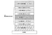
本実施例では、本発明のピレン誘導体を、発光物質を含む層の一部に用いて発光素子を作製する場合であって、具体的には、本発明のピレン誘導体を発光層として用いる場合の素子構造について図1を用いて説明する。 In this embodiment, a light-emitting element is manufactured using the pyrene derivative of the present invention as part of a layer containing a light-emitting substance. Specifically, the case of using the pyrene derivative of the present invention as a light-emitting layer is described. The element structure will be described with reference to FIG.
まず、基板100上に発光素子の第1の電極101が形成される。なお、本実施例では、第1の電極101は陽極として機能する。材料として透明導電膜であるITOを用い、スパッタリング法により110nmの膜厚で形成する。
First, the first electrode 101 of the light emitting element is formed over the
次に、第1の電極(陽極)101上に発光物質を含む層102が形成される。なお、本実施例における発光物質を含む層102は、正孔注入層111、正孔輸送層112、発光層113、正孔阻止層(ホールブロッキング層)114、電子輸送層115、電子注入層116からなる積層構造を有している。
Next, a
第1の電極101が形成された基板を市販の真空蒸着装置の基板ホルダーに第1の電極101が形成された面を下方にして固定し、真空蒸着装置の内部に備えられた蒸発源に銅フタロシアニン(以下、Cu−Pcと示す)を入れ、抵抗加熱法を用いた蒸着法により20nmの膜厚で正孔注入層111を形成する。なお、正孔注入層111を形成する材料としては、公知の正孔注入性材料を用いることができる。
The substrate on which the first electrode 101 is formed is fixed to a substrate holder of a commercially available vacuum deposition apparatus with the surface on which the first electrode 101 is formed facing downward, and copper is attached to the evaporation source provided in the vacuum deposition apparatus. Phthalocyanine (hereinafter referred to as Cu-Pc) is added, and the
次に正孔輸送性に優れた材料により正孔輸送層112を形成する。正孔輸送層112を形成する材料としては、公知の正孔輸送性材料を用いることができるが、本実施例では、α−NPDを用いて、40nmの膜厚で形成する。 Next, the hole transport layer 112 is formed using a material having excellent hole transportability. As a material for forming the hole transport layer 112, a known hole transport material can be used. In this embodiment, α-NPD is used to form a film with a thickness of 40 nm.
次に発光層113を形成する。なお、発光層113において正孔と電子が再結合し、発光を生じる。本実施例では、発光層113を形成する材料に本発明のピレン誘導体として、TBiPyを用い、30nmの膜厚で蒸着法により形成する。
Next, the
次に、正孔阻止層114を形成する。正孔阻止層114を形成する材料としては、公知の電子輸送性材料を用いることができるが、本実施例では、BAlqを用い、10nmの膜厚で蒸着法により形成する。 Next, the hole blocking layer 114 is formed. As a material for forming the hole blocking layer 114, a known electron transporting material can be used. In this embodiment, BAlq is used and a film thickness of 10 nm is formed by an evaporation method.
次に、電子輸送層115を形成する。電子輸送層115を形成する材料としては、公知の電子輸送性材料を用いることができるが、本実施例では、Alq3を用い、20nmの膜厚で蒸着法により形成する。 Next, the electron transport layer 115 is formed. As a material for forming the electron transport layer 115, a known electron transport material can be used. In this embodiment, Alq 3 is used and a film thickness of 20 nm is formed by a vapor deposition method.
次に、電子注入層116を形成する。電子注入層116を形成する材料としては、公知の電子注入性材料を用いることが出来るが、本実施例では、弗化カルシウム(以下、CaF2と示す)を用い、2nmの膜厚で蒸着法により形成する。 Next, the electron injection layer 116 is formed. As a material for forming the electron injection layer 116, a known electron injection material can be used. In this embodiment, calcium fluoride (hereinafter referred to as CaF 2 ) is used, and a deposition method is performed with a film thickness of 2 nm. To form.
このようにして、正孔注入層111、正孔輸送層112、発光層113、正孔阻止層114、電子輸送層115、および電子注入層116を積層して形成される発光物質を含む層102を形成した後、陰極として機能する第2の電極103をスパッタリング法または蒸着法により形成する。なお、本実施例では、発光物質を含む層102上にアルミニウム(150nm)を蒸着法により形成することにより第2の電極103を得る。
In this manner, the
以上により、本発明のピレン誘導体を用いた発光素子が形成される。 Thus, a light-emitting element using the pyrene derivative of the present invention is formed.
また、形成された発光素子に電圧を印加すると、該発光素子においては、電圧5V以上で青色発光が観測され、印加電圧10Vにおいて発光輝度2098cd/m2の青色発光(発光のCIE色座標:x=0.169、y=0.162)が観測された。その時の発光効率は1.03cd/Aであった。 When a voltage is applied to the formed light-emitting element, blue light emission is observed at a voltage of 5 V or more at the light-emitting element, and blue light emission with an emission luminance of 2098 cd / m 2 at the applied voltage of 10 V (light emission CIE color coordinate: x = 0.169, y = 0.162) were observed. The luminous efficiency at that time was 1.03 cd / A.
本実施例では、発光層のゲスト材料として本発明のピレン誘導体を用いる場合について、図6を用いて説明する。本実施例では、第1の電極、第2の電極、正孔注入層、正孔輸送層、正孔阻止層、電子輸送層、電子注入層の構成については、実施例1と同様であるので説明は省略する。 In this example, the case of using the pyrene derivative of the present invention as the guest material of the light-emitting layer will be described with reference to FIGS. In this example, the configurations of the first electrode, the second electrode, the hole injection layer, the hole transport layer, the hole blocking layer, the electron transport layer, and the electron injection layer are the same as in Example 1. Description is omitted.
図6に示すように、第1の電極201上に形成される発光物質を含む層202のうち、正孔輸送層212と接して形成される発光層213は、ホスト材料と本発明のピレン誘導体であるゲスト材料を用いることにより形成する。
As shown in FIG. 6, the light emitting layer 213 formed in contact with the hole transport layer 212 in the
具体的には、ホスト材料としてCBPを、ゲスト材料としてTBiPyを用い、30nmの膜厚で共蒸着法により形成する。ゲスト材料の割合は5wt%とした。 Specifically, CBP is used as a host material, TBiPy is used as a guest material, and a film thickness of 30 nm is formed by a co-evaporation method. The ratio of the guest material was 5 wt%.
このようにして、正孔注入層211、正孔輸送層212、発光層213、正孔阻止層214、電子輸送層215、および電子注入層216を積層して形成される発光物質を含む層202上に第2の電極203を形成することにより、基板200上に、本発明のピレン誘導体を用いた発光素子が形成される。
In this manner, the
形成された発光素子に電圧を印加すると、該発光素子においては、電圧7V以上で青色発光が観測され、印加電圧10Vにおいて発光輝度74cd/m2の青色発光(発光のCIE色座標:x=0.170、y=0.159)が観測された。この時の発光効率は1.43cd/Aであった。 When a voltage is applied to the formed light emitting element, blue light emission is observed at a voltage of 7 V or more at the light emitting element, and blue light emission (light emission CIE color coordinate: x = 0) at an emission voltage of 74 cd / m 2 is applied. 170, y = 0.159) was observed. The luminous efficiency at this time was 1.43 cd / A.
本発明のピレン誘導体は効率の良い発光性を有することから、本実施例に示すように発光物質を含む層の発光層におけるゲスト材料として用いることができる。また、本発明のピレン誘導体は、優れた耐熱性を有し、かつ成膜した際に結晶化しにくいことから、発光素子の長寿命化を図ることができる。 Since the pyrene derivative of the present invention has an efficient light-emitting property, it can be used as a guest material in a light-emitting layer including a light-emitting substance as shown in this embodiment. In addition, since the pyrene derivative of the present invention has excellent heat resistance and is difficult to crystallize when formed, the lifetime of the light-emitting element can be increased.
(比較例1)
本比較例では、発光層のゲスト材料として1、3、6、8―テトラ(4−ビフェニリル)ピレン(以下、t(bp)pyと示す)を用いる場合であって、他の構成は実施例3と同様とした素子について図7を用いて説明する。
(Comparative Example 1)
In this comparative example, 1, 3, 6, 8-tetra (4-biphenylyl) pyrene (hereinafter referred to as t (bp) py) is used as the guest material of the light emitting layer, and the other configuration is the example. An element similar to 3 is described with reference to FIG.
図7に示すように、第1の電極301上に形成される発光物質を含む層302のうち、正孔輸送層312と接して形成される発光層313は、ホスト材料と本比較例のt(bp)pyであるゲスト材料を用いることにより形成する。
As shown in FIG. 7, the light-emitting
具体的には、ホスト材料としてCBPを、ゲスト材料としてt(bp)pyを用い、30nmの膜厚で共蒸着法により形成する。ゲスト材料の割合は、実施例3と同様に5wt%とした。 Specifically, CBP is used as a host material, t (bp) py is used as a guest material, and a film thickness of 30 nm is formed by a co-evaporation method. The ratio of the guest material was 5 wt% as in Example 3.
このようにして、正孔注入層311、正孔輸送層312、発光層313、正孔阻止層314、電子輸送層315、および電子注入層316を積層して形成される発光物質を含む層302上に第2の電極303を形成することにより、基板300上に、t(bp)pyを用いた発光素子が形成される。
In this manner, the
形成された発光素子に電圧を印加すると、該発光素子においては、電圧6V以上で青色発光が観測され、印加電圧10Vにおいて発光輝度296cd/m2の青色発光(発光のCIE色座標:x=0.154、y=0.140)が観測された。この時の発光効率は1.03cd/Aであり、同様の素子構成である実施例3に比べてやや劣っていた。さらにこの発光素子は、実施例2〜3の場合に比べて膜質が劣化していた。 When a voltage is applied to the formed light-emitting element, blue light emission is observed at a voltage of 6 V or more in the light-emitting element, and blue light emission (light emission CIE color coordinate: x = 0) at an emission voltage of 296 cd / m 2 is applied. .154, y = 0.140). The luminous efficiency at this time was 1.03 cd / A, which was slightly inferior to that of Example 3 having the same element configuration. Furthermore, the film quality of this light emitting device was deteriorated as compared with the cases of Examples 2-3.
本実施例では、画素部に本発明の発光素子を有する発光装置について図8を用いて説明する。なお、図8(A)は、発光装置を示す上面図、図8(B)は図8(A)をA−A’で切断した断面図である。点線で示された601は駆動回路部(ソース側駆動回路)、602は画素部、603は駆動回路部(ゲート側駆動回路)である。また、604は封止基板、605はシール材であり、シール材605で囲まれた内側は、空間607になっている。
In this embodiment, a light-emitting device having the light-emitting element of the present invention in a pixel portion will be described with reference to FIG. 8A is a top view illustrating the light-emitting device, and FIG. 8B is a cross-sectional view taken along line A-A ′ in FIG. 8A. Reference numeral 601 indicated by a dotted line denotes a driving circuit portion (source side driving circuit), 602 denotes a pixel portion, and 603 denotes a driving circuit portion (gate side driving circuit). Reference numeral 604 denotes a sealing substrate,
なお、引き回し配線608はソース側駆動回路601及びゲート側駆動回路603に入力される信号を伝送するための配線であり、外部入力端子となるFPC(フレキシブルプリントサーキット)609からビデオ信号、クロック信号、スタート信号、リセット信号等を受け取る。なお、ここではFPCしか図示されていないが、このFPCにはプリント配線基盤(PWB)が取り付けられていても良い。本明細書における発光装置には、発光装置本体だけでなく、それにFPCもしくはPWBが取り付けられた状態をも含むものとする。 Note that the routing wiring 608 is a wiring for transmitting a signal input to the source side driving circuit 601 and the gate side driving circuit 603, and a video signal, a clock signal, an FPC (flexible printed circuit) 609 serving as an external input terminal, Receives start signal, reset signal, etc. Although only the FPC is shown here, a printed wiring board (PWB) may be attached to the FPC. The light-emitting device in this specification includes not only a light-emitting device body but also a state in which an FPC or a PWB is attached thereto.
次に、断面構造について図8(B)を用いて説明する。素子基板610上には駆動回路部及び画素部が形成されているが、ここでは、駆動回路部であるソース側駆動回路601と、画素部602が示されている。
Next, a cross-sectional structure is described with reference to FIG. A driver circuit portion and a pixel portion are formed over the
なお、ソース側駆動回路601はnチャネル型TFT623とpチャネル型TFT624とを組み合わせたCMOS回路が形成される。また、駆動回路を形成するTFTは、公知のCMOS回路、PMOS回路もしくはNMOS回路で形成しても良い。また、本実施例では、基板上に駆動回路を形成したドライバー一体型を示すが、必ずしもその必要はなく、基板上ではなく外部に形成することもできる。
Note that the source side driver circuit 601 is a CMOS circuit in which an n-
また、画素部602はスイッチング用TFT611と、電流制御用TFT612とそのドレインに電気的に接続された第1の電極613とを含む複数の画素により形成される。なお、第1の電極613の端部を覆って絶縁物614が形成されている。ここでは、ポジ型の感光性アクリル樹脂膜を用いることにより形成する。
The pixel portion 602 is formed by a plurality of pixels including a switching
また、成膜性を良好なものとするため、絶縁物614の上端部または下端部に曲率を有する曲面が形成されるようにする。例えば、絶縁物614の材料としてポジ型の感光性アクリルを用いた場合、絶縁物614の上端部のみに曲率半径(0.2μm〜3μm)を有する曲面を持たせることが好ましい。また、絶縁物614として、感光性の光によってエッチャントに不溶解性となるネガ型、或いは光によってエッチャントに溶解性となるポジ型のいずれも使用することができる。 In order to improve the film forming property, a curved surface having a curvature is formed at the upper end portion or the lower end portion of the insulator 614. For example, when positive photosensitive acrylic is used as a material for the insulator 614, it is preferable that only the upper end portion of the insulator 614 has a curved surface with a curvature radius (0.2 μm to 3 μm). As the insulator 614, either a negative type that becomes insoluble in an etchant by photosensitive light or a positive type that becomes soluble in an etchant by light can be used.
第1の電極613上には、発光物質を含む層616、および第2の電極617がそれぞれ形成されている。ここで、陽極として機能する第1の電極613に用いる材料としては、仕事関数の大きい材料を用いることが望ましい。例えば、ITO膜、2〜20%の酸化亜鉛を含む酸化インジウム膜、窒化チタン膜、クロム膜、タングステン膜、Zn膜、Pt膜などの単層膜の他、窒化チタン膜とアルミニウムを主成分とする膜との積層、窒化チタン膜とアルミニウムを主成分とする膜と窒化チタン膜との3層構造等を用いることができる。なお、積層構造とすると、配線としての抵抗も低く、良好なオーミックコンタクトがとれ、さらに陽極として機能させることができる。 Over the first electrode 613, a layer 616 containing a light-emitting substance and a second electrode 617 are formed. Here, as a material used for the first electrode 613 functioning as an anode, a material having a high work function is preferably used. For example, in addition to a single layer film such as an ITO film, an indium oxide film containing 2 to 20% zinc oxide, a titanium nitride film, a chromium film, a tungsten film, a Zn film, or a Pt film, a titanium nitride film and aluminum are the main components. For example, a three-layer structure including a titanium nitride film, a film containing aluminum as its main component, and a titanium nitride film can be used. Note that with a stacked structure, resistance as a wiring is low, good ohmic contact can be obtained, and a function as an anode can be obtained.
また、発光物質を含む層616は、蒸着マスクを用いた蒸着法、またはインクジェット法によって形成される。発光物質を含む層616には、本発明のピレン誘導体が含まれる。また、これらのピレン誘導体に組み合わせて用いる材料としては、低分子系材料、中分子材料(オリゴマー、デンドリマーを含む)、または高分子系材料であっても良い。また、発光物質を含む層に用いる材料としては、通常、有機化合物を単層もしくは積層で用いる場合が多いが、本発明においては、有機化合物からなる膜の一部に無機化合物を用いる構成も含めることとする。 The layer 616 containing a light-emitting substance is formed by an evaporation method using an evaporation mask or an inkjet method. The layer 616 containing a light-emitting substance contains the pyrene derivative of the present invention. The material used in combination with these pyrene derivatives may be a low molecular material, a medium molecular material (including oligomers and dendrimers), or a high molecular material. In addition, as a material used for a layer including a light-emitting substance, an organic compound is usually used in a single layer or a stacked layer. However, in the present invention, a structure in which an inorganic compound is used for part of a film formed of an organic compound is also included. I will do it.
さらに、発光物質を含む層616上に形成される第2の電極(陰極)617に用いる材料としては、仕事関数の小さい材料(Al、Ag、Li、Ca、またはこれらの合金MgAg、MgIn、AlLi、CaF2、またはCaN)を用いればよい。なお、発光物質を含む層616で生じた光が第2の電極617を透過させる場合には、第2の電極(陰極)617として、膜厚を薄くした金属薄膜と、透明導電膜(ITO、2〜20%の酸化亜鉛を含む酸化インジウム、酸化亜鉛(ZnO)等)との積層を用いるのが良い。 Furthermore, as a material used for the second electrode (cathode) 617 formed over the layer 616 containing a light-emitting substance, a material having a low work function (Al, Ag, Li, Ca, or alloys thereof MgAg, MgIn, AlLi , CaF 2 , or CaN) may be used. Note that in the case where light generated in the layer 616 containing a light-emitting substance passes through the second electrode 617, a thin metal film and a transparent conductive film (ITO, A stack with indium oxide containing 2 to 20% zinc oxide, zinc oxide (ZnO), or the like is preferably used.
さらにシール材605で封止基板604を素子基板610と貼り合わせることにより、素子基板610、封止基板604、およびシール材605で囲まれた空間607に発光素子618が備えられた構造になっている。なお、空間607には、不活性気体(窒素やアルゴン等)が充填される場合の他、シール材605で充填される構成も含むものとする。
Further, the sealing substrate 604 is bonded to the
なお、シール材605にはエポキシ系樹脂を用いるのが好ましい。また、これらの材料はできるだけ水分や酸素を透過しない材料であることが望ましい。また、封止基板604に用いる材料としてガラス基板や石英基板の他、FRP(Fiberglass−Reinforced Plastics)、PVF(ポリビニルフロライド)、マイラー、ポリエステルまたはアクリル等からなるプラスチック基板を用いることができる。
Note that an epoxy-based resin is preferably used for the
以上のようにして、本発明の発光素子を有する発光装置を得ることができる。このような本発明を用いた発光装置は、発光素子における結晶化が抑制されているため、長時間に渡って安定な発光を得ることができる。 As described above, a light-emitting device having the light-emitting element of the present invention can be obtained. In such a light-emitting device using the present invention, since crystallization in the light-emitting element is suppressed, stable light emission can be obtained for a long time.
なお、本実施例に示す発光装置は、実施例1〜実施例3に示した発光素子の構成を自由に組み合わせて実施することが可能である。
Note that the light-emitting device described in this embodiment can be implemented by freely combining the structures of the light-emitting elements described in
本実施例では、本発明で発光素子を有する発光装置を用いて完成させた様々な電気器具について説明する。 In this embodiment, various electric appliances completed using a light-emitting device having a light-emitting element according to the present invention will be described.
本発明を用いて形成される発光装置を実装した電気器具として、ビデオカメラ、デジタルカメラ、ゴーグル型ディスプレイ、ナビゲーションシステム、音響再生装置(カーオーディオ、オーディオコンポ等)、パーソナルコンピュータ、ゲーム機器、携帯情報端末(モバイルコンピュータ、携帯電話、携帯型ゲーム機または電子書籍等)、記録媒体を備えた画像再生装置(具体的にはデジタルビデオディスク(DVD)等の記録媒体を再生し、その画像を表示しうる表示装置を備えた装置)などが挙げられる。図9にこれらの電子機器のうち一部のものについて例示し、説明する。 As an electric appliance in which a light emitting device formed using the present invention is mounted, a video camera, a digital camera, a goggle type display, a navigation system, a sound reproduction device (car audio, audio component, etc.), a personal computer, a game machine, portable information A terminal (mobile computer, mobile phone, portable game machine, electronic book, etc.), an image playback device equipped with a recording medium (specifically, a recording medium such as a digital video disc (DVD)) is played back, and the image is displayed. And a display device). FIG. 9 illustrates and describes some of these electronic devices.
図9(A)は表示装置であり、筐体2001、支持台2002、表示部2003、スピーカー部2004、ビデオ入力端子2005等を含む。本発明を用いて形成される発光装置をその表示部2003に用いることにより作製される。なお、表示装置は、コンピュータ用、TV放送受信用、広告表示用などの全ての情報表示用装置が含まれる。
FIG. 9A illustrates a display device, which includes a
ここで、図9(B)は携帯電話であり、本体2701、筐体2702、表示部2703、音声入力部2704、音声出力部2705、操作キー2706、外部接続ポート2707、アンテナ2708等を含む。本発明の発光素子を有する発光装置をその表示部2703に用いることにより作製される。
Here, FIG. 9B shows a mobile phone, which includes a
以上の様に、本発明の発光素子を有する発光装置の適用範囲は極めて広く、また発光装置に用いる発光素子は、本発明のピレン誘導体を用いて形成されるため、駆動電圧が低く、長寿命であるという特徴を有している。従って、この発光装置をあらゆる分野の電気器具に適用することにより、低消費電力化、長寿命化(つまり長期間良好な表示画像を得ることができる)を実現することができる。 As described above, the applicable range of the light-emitting device having the light-emitting element of the present invention is extremely wide, and the light-emitting element used for the light-emitting device is formed using the pyrene derivative of the present invention, and thus has a low driving voltage and a long lifetime. It has the feature of being. Therefore, by applying this light-emitting device to electric appliances in various fields, low power consumption and long life (that is, a good display image can be obtained for a long time) can be realized.
100 基板
101 第1の電極
102 発光物質を含む層
103 第2の電極
111 正孔注入層
112 正孔輸送層
113 発光層
114 正孔阻止層
115 電子輸送層
116 電子注入層
DESCRIPTION OF
Claims (5)
An electric appliance having the light emitting device according to any one of claims 1 to 4, wherein the video camera, a digital camera, a goggle type display, a navigation system, a sound reproducing device, a personal computer, a game machine, and portable information An electric appliance selected from an image reproducing device provided with a terminal and a recording medium.
Priority Applications (1)
| Application Number | Priority Date | Filing Date | Title |
|---|---|---|---|
| JP2004289684A JP2005126431A (en) | 2003-10-03 | 2004-10-01 | Pyrene derivative, light-emitting element, light-emitting device, and electric appliance |
Applications Claiming Priority (2)
| Application Number | Priority Date | Filing Date | Title |
|---|---|---|---|
| JP2003345195 | 2003-10-03 | ||
| JP2004289684A JP2005126431A (en) | 2003-10-03 | 2004-10-01 | Pyrene derivative, light-emitting element, light-emitting device, and electric appliance |
Publications (2)
| Publication Number | Publication Date |
|---|---|
| JP2005126431A true JP2005126431A (en) | 2005-05-19 |
| JP2005126431A5 JP2005126431A5 (en) | 2007-10-18 |
Family
ID=34655846
Family Applications (1)
| Application Number | Title | Priority Date | Filing Date |
|---|---|---|---|
| JP2004289684A Withdrawn JP2005126431A (en) | 2003-10-03 | 2004-10-01 | Pyrene derivative, light-emitting element, light-emitting device, and electric appliance |
Country Status (1)
| Country | Link |
|---|---|
| JP (1) | JP2005126431A (en) |
Cited By (11)
| Publication number | Priority date | Publication date | Assignee | Title |
|---|---|---|---|---|
| JP2005294250A (en) * | 2004-03-10 | 2005-10-20 | Fuji Photo Film Co Ltd | Light emitting element |
| WO2006057326A1 (en) * | 2004-11-25 | 2006-06-01 | Pioneer Corporation | Pyrene compound and light emitting transistor device utilizing the same |
| WO2006057325A1 (en) * | 2004-11-25 | 2006-06-01 | Pioneer Corporation | Pyrene compound and, utilizing the same, light emitting transistor device and electroluminescence device |
| WO2007004799A1 (en) * | 2005-06-30 | 2007-01-11 | Lg Chem. Ltd. | Pyrene derivatives and organic electronic device using pyrene derivatives |
| KR100747313B1 (en) | 2005-07-15 | 2007-08-07 | 엘지전자 주식회사 | Electron Transport Chemical and Organic Light Emitting Device comprising the same |
| JPWO2007029798A1 (en) * | 2005-09-08 | 2009-03-19 | 東レ株式会社 | Light emitting device material and light emitting device |
| US7651789B2 (en) | 2004-03-10 | 2010-01-26 | Fujifilm Corporation | Organic electroluminescent device |
| WO2011077689A1 (en) | 2009-12-21 | 2011-06-30 | 出光興産株式会社 | Pyrene derivative and organic electroluminescent element using the same |
| WO2011077690A1 (en) | 2009-12-21 | 2011-06-30 | 出光興産株式会社 | Pyrene derivative and organic electroluminescent element using the same |
| US9353027B2 (en) | 2009-12-21 | 2016-05-31 | Idemitsu Kosan Co., Ltd. | Organic electroluminescent element using pyrene derivative |
| WO2020039708A1 (en) | 2018-08-23 | 2020-02-27 | 国立大学法人九州大学 | Organic electroluminescence element |
-
2004
- 2004-10-01 JP JP2004289684A patent/JP2005126431A/en not_active Withdrawn
Cited By (17)
| Publication number | Priority date | Publication date | Assignee | Title |
|---|---|---|---|---|
| US7651789B2 (en) | 2004-03-10 | 2010-01-26 | Fujifilm Corporation | Organic electroluminescent device |
| JP2005294250A (en) * | 2004-03-10 | 2005-10-20 | Fuji Photo Film Co Ltd | Light emitting element |
| WO2006057326A1 (en) * | 2004-11-25 | 2006-06-01 | Pioneer Corporation | Pyrene compound and light emitting transistor device utilizing the same |
| WO2006057325A1 (en) * | 2004-11-25 | 2006-06-01 | Pioneer Corporation | Pyrene compound and, utilizing the same, light emitting transistor device and electroluminescence device |
| JP2006176491A (en) * | 2004-11-25 | 2006-07-06 | Kyoto Univ | Pyrene based compound and light emitting transistor device utilizing the same |
| US7745819B2 (en) | 2005-06-30 | 2010-06-29 | Lg Chem. Ltd. | Pyrene derivatives and organic electronic device using pyrene derivatives |
| WO2007004799A1 (en) * | 2005-06-30 | 2007-01-11 | Lg Chem. Ltd. | Pyrene derivatives and organic electronic device using pyrene derivatives |
| USRE44824E1 (en) | 2005-06-30 | 2014-04-08 | Lg Chem, Ltd. | Pyrene derivatives and organic electronic device using pyrene derivatives |
| CN101080478B (en) * | 2005-06-30 | 2014-07-30 | Lg化学株式会社 | Pyrene derivatives and organic electronic device using pyrene derivatives |
| KR100747313B1 (en) | 2005-07-15 | 2007-08-07 | 엘지전자 주식회사 | Electron Transport Chemical and Organic Light Emitting Device comprising the same |
| JPWO2007029798A1 (en) * | 2005-09-08 | 2009-03-19 | 東レ株式会社 | Light emitting device material and light emitting device |
| JP5029013B2 (en) * | 2005-09-08 | 2012-09-19 | 東レ株式会社 | Light emitting device material and light emitting device |
| WO2011077689A1 (en) | 2009-12-21 | 2011-06-30 | 出光興産株式会社 | Pyrene derivative and organic electroluminescent element using the same |
| WO2011077690A1 (en) | 2009-12-21 | 2011-06-30 | 出光興産株式会社 | Pyrene derivative and organic electroluminescent element using the same |
| US9169274B2 (en) | 2009-12-21 | 2015-10-27 | Idemitsu Kosan Co., Ltd. | Pyrene derivative and organic electroluminescent element using the same |
| US9353027B2 (en) | 2009-12-21 | 2016-05-31 | Idemitsu Kosan Co., Ltd. | Organic electroluminescent element using pyrene derivative |
| WO2020039708A1 (en) | 2018-08-23 | 2020-02-27 | 国立大学法人九州大学 | Organic electroluminescence element |
Similar Documents
| Publication | Publication Date | Title |
|---|---|---|
| US7232619B2 (en) | Pyrene derivative, light emitting element, and light emitting device | |
| JP4558510B2 (en) | Carbazole derivatives, light emitting devices and electronic devices | |
| US8084145B2 (en) | Organometallic complex, light emitting element using the complex, light emitting device using the element, and electric apparatus using the device | |
| JP6010150B2 (en) | Light emitting element | |
| EP1690866B1 (en) | Organic metal complex and light-emitting device using same | |
| JP4366332B2 (en) | Organometallic complex, light emitting element and light emitting device using the organometallic complex | |
| US7939821B2 (en) | Organometallic complex, and light emitting element and electronic appliance using the same | |
| KR101326286B1 (en) | Light emitting element and light emitting device | |
| JP2005026221A (en) | Electron injection composition for light emitting element, light emitting element, and light emitting device | |
| JP4401665B2 (en) | Electroluminescent device | |
| JP4391421B2 (en) | Electroluminescent device and light emitting device | |
| JP2005154421A (en) | Carbazole derivative, light-emitting element, and light-emitting device | |
| JP2005126431A (en) | Pyrene derivative, light-emitting element, light-emitting device, and electric appliance | |
| JP4954623B2 (en) | Light emitting device | |
| WO2005040117A1 (en) | Carbazole derivative, light emitting element, and light emitting device | |
| JP4312678B2 (en) | Organometallic complex, and light emitting device and electronic device using the same | |
| JP4637510B2 (en) | LIGHT EMITTING ELEMENT AND LIGHT EMITTING DEVICE | |
| JP4912780B2 (en) | Organometallic complex, light-emitting element, light-emitting device, and electronic device | |
| JP4869690B2 (en) | LIGHT EMITTING ELEMENT, LIGHT EMITTING DEVICE AND COMPOSITE MATERIAL | |
| JP5171734B2 (en) | Electroluminescent device and light emitting device |
Legal Events
| Date | Code | Title | Description |
|---|---|---|---|
| A521 | Request for written amendment filed |
Free format text: JAPANESE INTERMEDIATE CODE: A523 Effective date: 20070903 |
|
| A621 | Written request for application examination |
Free format text: JAPANESE INTERMEDIATE CODE: A621 Effective date: 20070903 |
|
| A131 | Notification of reasons for refusal |
Free format text: JAPANESE INTERMEDIATE CODE: A131 Effective date: 20090526 |
|
| A761 | Written withdrawal of application |
Free format text: JAPANESE INTERMEDIATE CODE: A761 Effective date: 20090624 |