JP2005294017A - Socket for electric component - Google Patents
Socket for electric component Download PDFInfo
- Publication number
- JP2005294017A JP2005294017A JP2004107045A JP2004107045A JP2005294017A JP 2005294017 A JP2005294017 A JP 2005294017A JP 2004107045 A JP2004107045 A JP 2004107045A JP 2004107045 A JP2004107045 A JP 2004107045A JP 2005294017 A JP2005294017 A JP 2005294017A
- Authority
- JP
- Japan
- Prior art keywords
- socket
- floating plate
- electrical component
- package
- pressing
- Prior art date
- Legal status (The legal status is an assumption and is not a legal conclusion. Google has not performed a legal analysis and makes no representation as to the accuracy of the status listed.)
- Granted
Links
- 230000000149 penetrating effect Effects 0.000 claims description 3
- 238000000605 extraction Methods 0.000 abstract 1
- 230000000452 restraining effect Effects 0.000 abstract 1
- 229910000679 solder Inorganic materials 0.000 description 5
- 238000007689 inspection Methods 0.000 description 4
- 238000004804 winding Methods 0.000 description 3
- 238000003780 insertion Methods 0.000 description 2
- 230000037431 insertion Effects 0.000 description 2
- 238000004519 manufacturing process Methods 0.000 description 2
- 239000000463 material Substances 0.000 description 2
- 229920001721 polyimide Polymers 0.000 description 2
- 229920002379 silicone rubber Polymers 0.000 description 2
- 239000004945 silicone rubber Substances 0.000 description 2
- 238000010586 diagram Methods 0.000 description 1
- 239000011159 matrix material Substances 0.000 description 1
- 239000002184 metal Substances 0.000 description 1
- 230000002093 peripheral effect Effects 0.000 description 1
- 239000009719 polyimide resin Substances 0.000 description 1
Images

Landscapes
- Connecting Device With Holders (AREA)
Abstract
Description
本発明は、電気部品を検査する電気部品用ソケットに関し、詳しくは、押圧手段による押圧動作完了直前まで電気部品へ負荷が掛からないようにして押圧動作時の電気部品に対するダメージを抑制し、同時に電気部品の取り出しを容易にしようとする電気部品用ソケットに係るものである。 The present invention relates to an electrical component socket for inspecting electrical components. More specifically, the present invention relates to an electrical component socket that suppresses damage to an electrical component during the pressing operation so that no load is applied to the electrical component until immediately before the pressing operation by the pressing means is completed. The present invention relates to an electrical component socket that is intended to facilitate the removal of the component.
従来の電気部品用ソケットは、例えば図10に示すように、コンタクトピン1が配設されたベースプレート2と、このベースプレート2上に配設され、電気部品(以下、ICパッケージ3と記載)の端子とコンタクトピン1とを電気的に接続するタブフィルム4と、このタブフィルム4上にベースプレート2に対して着脱可能に配設され、一側端部に回動可能にソケットカバー5を設けた中間部材6と、この中間部材6に設けた開口部6aに着脱可能に係合され、中央部に開口部7aが形成されたアライメントプレート7とを有しており、ソケットカバー5を倒伏して閉じることによって、ソケットカバー5に設けたパッド8でアライメントプレート7の開口部7aに収容されたICパッケージ3を押圧して、タブフィルム4を介してICパッケージ3の端子とコンタクトピン1とを電気的に接続させるようになっている(例えば、特許文献1参照)。
For example, as shown in FIG. 10, a conventional socket for electric parts is provided with a
なお、図10において、符号9は、タブフィルム4を下から弾性的に支持してタブフィルム4の電極パターン(以下、接点電極4aと記載)とICパッケージ3の端子との確実な電気的接続を確保するために設けたシリコーンゴム等からなる弾性シートを示している。また、符号10は、ICパッケージ3の端子が所定以上潰れないように設けたストッパを示している。さらに、符号11は、中間部材6に押圧されてタブフィルム4の接続電極4bとコンタクトピン1との確実な電気的接続を維持するために設けた他の弾性シートを示している。また、符号12は、中間部材の側面6bに係止してソケットカバーの閉状態を維持するようにした係止手段を示している。そして、上記各要素は、ボルト13とナット14とを締結して電気部品用ソケットに組立てられる。
しかし、このような従来の電気部品用ソケットにおいては、ICパッケージ3を押圧してICパッケージ3の端子である半田ボールとタブフィルム4の接点電極4aとの電気的接続を確保するようにしたものであるため、例えば高温で行うバーンインテスト等の際に半田ボールが軟化して接点電極4aに貼りつくことがあった。この場合、テスト終了後、ICパッケージ3を電気部品用ソケットから取り外す際に、容易に取り出せないことがあった。
However, in such a conventional socket for electrical parts, the
このような問題に対処するためには、図11に示すように、前述のアライメントプレート7に替えて、弦巻ばね15で上方に付勢されて弾性的に支持され、上下動可能にされたフローティングプレート16をベースプレート2上方に配設し、このフローティングプレート16のICパッケージ3を収容する開口部16aの壁部16bにICパッケージ3の底面に係止する支持部17を開口部16a内側に突出させる構成とすることが考えられる。このように構成すれば、ソケットカバー5を閉じるときに、開口部16aに収容されたICパッケージ3の上面をパッド8で弦巻ばね15の同図中矢印A方向の付勢力に抗して同図中矢印B方向に押圧してフローティングプレート16と一緒に押し下げ、ICパッケージ3の端子3aとタブフィルム4の接点電極4aとを接続させることができる。また、テスト終了後は、ソケットカバー5を開く動作に伴って、パッド8によるICパッケージ3への押圧力が解除され、弦巻ばね15の付勢力(矢印A方向)によりフローティングプレート16が押し上げられる。これにより、フローティングプレート16の開口部16aに設けた支持部17がICパッケージ3の底面に係止して、タブフィルム4の接点電極4aに貼りついたICパッケージ3の端子3aを弦巻ばね15の付勢力によって引き剥がすことができる。
In order to cope with such a problem, as shown in FIG. 11, instead of the
しかし、このような電気部品用ソケットにおいては、貼りついたICパッケージ3を容易に引き剥がすためには、弦巻ばね15の付勢力を強くする必要がある。この場合、ICパッケージ3をフローティングプレート16の開口部16aに収容してソケットカバー5を閉じる際に、ICパッケージ3には、矢印A方向の弦巻ばね15の付勢力がそのまま作用することになり、ICパッケージ3の底面部に大きなダメージを与え、ICパッケージ3を破損させたり傷付けたりする虞がある。
However, in such an electrical component socket, it is necessary to increase the urging force of the
そこで、本発明は、このような問題点に対処し、押圧手段による押圧動作時の電気部品に対するダメージを抑制し、同時に電気部品の取り出しを容易にしようとする電気部品用ソケットを提供することを目的とする。 Accordingly, the present invention provides an electrical component socket that addresses such problems, suppresses damage to the electrical component during the pressing operation by the pressing means, and at the same time facilitates the removal of the electrical component. Objective.
上記目的を達成するために、本発明による電気部品用ソケットは、ソケット本体部の上面に形成され、電気部品を収容し、該電気部品の端子と接触可能なコンタクト手段を配設した収容部と、前記収容部に対して上下動可能に配設され、前記電気部品の底面に係止してこれを支持するフローティングプレートと、前記ソケット本体部に備えられ、前記フローティングプレートを上方に付勢する付勢手段と、前記収容部に収容される電気部品に対して、その上面を押圧して電気部品の端子と前記コンタクト手段とを電気的に接続させるように上方から押圧する押圧手段と、を備えて成る電気部品用ソケットであって、前記押圧手段が前記電気部品を押圧する際、該電気部品の上面に前記押圧手段が当接して押圧する前に、前記フローティングプレートを下降させる手段を備えたものである。 In order to achieve the above object, an electrical component socket according to the present invention is formed on an upper surface of a socket main body portion, accommodates an electrical component, and includes an accommodating portion provided with contact means capable of contacting the terminal of the electrical component. A floating plate that is arranged to be movable up and down with respect to the housing part, and that is engaged with and supports the bottom surface of the electrical component, and is provided in the socket body part, and biases the floating plate upward. Urging means and pressing means for pressing from above the electrical component housed in the housing portion so as to press the upper surface thereof to electrically connect the terminal of the electrical component and the contact means. When the pressing means presses the electrical component, the floating part is provided before the pressing means contacts and presses the upper surface of the electrical component. Those having means for lowering the over bets.
このような構成により、付勢手段で付勢されて収容部に対して上下動可能に配設されたフローティングプレートで電気部品の底面に係止してこれを支持し、押圧手段が電気部品を押圧する際、電気部品の上面に押圧手段が当接して押圧する前に、フローティングプレートを下降させる手段でフローティングプレートを下降させる。 With such a configuration, the floating plate that is urged by the urging means and is arranged so as to be movable up and down with respect to the accommodating portion is locked to and supported by the bottom surface of the electric component, and the pressing means holds the electric component. When pressing, the floating plate is lowered by the means for lowering the floating plate before the pressing means comes into contact with the upper surface of the electrical component and presses it.
また、前記フローティングプレートを下降させる手段は、前記フローティングプレートの前記付勢手段に対応する部位に上下方向に貫通した貫通孔に挿入されて前記付勢手段の付勢を解除する解除部材であり、前記電気部品の上面に押圧手段が当接して押圧する前に、該押圧手段によって押圧されて付勢手段の付勢を解除するようにしたものである。これにより、押圧手段でフローティングプレートに設けた上下方向の貫通孔に挿入された解除部材を電気部品が押圧される前に押圧し、解除部材でフローティングプレートを上方に付勢する付勢手段の付勢を解除する。 Further, the means for lowering the floating plate is a release member that is inserted into a through-hole penetrating in a vertical direction in a portion corresponding to the biasing means of the floating plate and releases the bias of the biasing means, Before the pressing means comes into contact with and presses on the upper surface of the electrical component, the pressing means presses the biasing means to release the biasing means. Thus, the pressing member presses the release member inserted into the vertical through-hole provided in the floating plate before the electric component is pressed, and the release member biases the floating plate upward. Release the force.
さらに、前記押圧手段は、前記ソケット本体の一側端部に回動可能に設けたソケットカバーの前記収容部に対向する側の面に弾性部材で弾性的に支持されたプッシャーと、該プッシャーに保持されて前記電気部品を押圧するパッドとを備え、前記ソケットカバーが倒伏する閉動作に伴って、前記パッドの縁部を前記解除部材に当接させて押圧するようにしたものである。これにより、ソケットカバーが倒伏する閉動作に伴って、ソケットカバーの収容部に対向する側の面にプッシャーと共に弾性的に支持されたパッドの縁部で解除部材を押圧する。 Further, the pressing means includes a pusher elastically supported by an elastic member on a surface of the socket cover that is rotatably provided at one end of the socket body and facing the accommodating portion, and the pusher A pad that is held and presses the electrical component, and the edge of the pad is pressed against the release member when the socket cover is closed. As a result, the release member is pressed by the edge portion of the pad elastically supported together with the pusher on the surface of the socket cover facing the housing portion in accordance with the closing operation in which the socket cover falls.
さらにまた、前記解除部材は、前記フローティングプレートの貫通孔に係止するブロック状に形成したものである。これにより、フローティングプレートの貫通孔に係止するブロック状の解除部材でフローティングプレートを付勢する付勢手段の付勢を解除する。 Furthermore, the release member is formed in a block shape that is engaged with the through hole of the floating plate. Thereby, the urging | biasing of the urging means which urges | biases a floating plate with the block-shaped releasing member latched in the through-hole of a floating plate is cancelled | released.
又は、前記解除部材は、前記付勢手段の上端部に一体的に形成した密巻き部である。これにより、付勢手段の上端部に一体的に形成した密巻き部でフローティングプレートを付勢する付勢手段の付勢を解除する。 Alternatively, the release member is a tightly wound portion formed integrally with the upper end portion of the urging means. Thereby, the urging | biasing of the urging | biasing means which urges | biases a floating plate by the closely wound part integrally formed in the upper end part of the urging | biasing means is cancelled | released.
また、前記パッドは、前記電気部品の押圧状態にてパッドの前記縁部と前記フローティングプレートの貫通孔上端面との間に隙間が生じるように形成したものである。これにより、電気部品の押圧状態にてパッドの縁部とフローティングプレートの貫通孔上端面との間に隙間を生じさせる。 The pad is formed such that a gap is formed between the edge portion of the pad and the upper end surface of the through hole of the floating plate when the electric component is pressed. Thus, a gap is generated between the edge of the pad and the upper end surface of the through hole of the floating plate in the pressed state of the electrical component.
そして、前記フローティングプレートは、前記収容部に対応して前記電気部品を挿入可能な開口部を備え、該開口部の壁部に電気部品の底面に係止する支持部を開口部内側に突出させたものである。これにより、開口部の壁部に開口部内側に突出させて備えた支持部で開口部に挿入された電気部品の底面に係止してこれを支持する。 The floating plate includes an opening into which the electric component can be inserted corresponding to the housing portion, and a support portion that locks the bottom surface of the electric component is protruded inside the opening portion on the wall portion of the opening. It is a thing. Thus, the support portion provided on the wall portion of the opening portion so as to protrude inside the opening portion is engaged with and supported by the bottom surface of the electric component inserted into the opening portion.
請求項1に係る発明によれば、電気部品を支持し、付勢手段で上方に付勢されたフローティングプレートを電気部品が押圧される前に下降させるようにしたことにより、フローティングプレートが最下点の位置まで下降した後、押圧手段が電気部品の上面に当接して押圧するまでは、押圧手段の負荷が電気部品へ掛からないようにすることができる。したがって、押圧手段による押圧動作時には、電気部品に対して付勢手段の付勢力が作用せず、電気部品に対するダメージを抑制することができる。 According to the first aspect of the present invention, the floating plate is supported at the bottom, and the floating plate urged upward by the urging means is lowered before the electric component is pressed. It is possible to prevent the load of the pressing means from being applied to the electric component until the pressing means comes into contact with and presses the upper surface of the electrical component after descending to the point position. Therefore, during the pressing operation by the pressing means, the urging force of the urging means does not act on the electrical component, and damage to the electrical component can be suppressed.
また、請求項2に係る発明によれば、電気部品を押圧する押圧手段でフローティングプレートに設けた上下方向の貫通孔に挿入された解除部材を電気部品が押圧される前に押圧し、解除部材でフローティングプレートを付勢する付勢手段の付勢を解除するようにしたことにより、フローティングプレートを下降させる機構を簡単な構造とすることができる。
According to the invention of
さらに、請求項3に係る発明によれば、ソケットカバーが倒伏する閉動作に伴って、ソケットカバーの収容部に対向する側の面にプッシャーと共に弾性的に支持されたパッドの縁部で解除部材を押圧するようにしたことにより、クラムシェルタイプの電気部品用ソケットに容易に適用することができる。
Further, according to the invention according to
また、請求項4に係る発明によれば、解除部材をフローティングプレートの貫通孔に係止するブロック状に形成したことにより、解除部材は、貫通孔から抜け落ちることがない。したがって、解除部材の取り扱いが容易になる。
According to the invention of
さらに、請求項5に係る発明によれば、解除部材を付勢手段の上端部に一体的に形成した密巻き部としたことにより、製造が容易である。
Furthermore, according to the invention which concerns on
また、請求項6に係る発明によれば、パッドによる電気部品の押圧状態にて該パッドの縁部と、フローティングプレートの貫通孔上端面との間に隙間が生じるようにしたことにより、電気部品の厚みのバラツキを吸収してパッドによる押圧力を確実に電気部品に伝えることができる。 According to the sixth aspect of the present invention, there is provided a gap between the edge of the pad and the upper end surface of the through hole of the floating plate when the electric component is pressed by the pad. It is possible to absorb the variation in thickness of the pad and reliably transmit the pressing force by the pad to the electrical component.
そして、請求項7に係る発明によれば、開口部の壁部に開口部内側に突出させて備えた支持部で開口部に挿入された電気部品をその底面に係止して支持するようにしたことにより、ソケットカバーの開動作時に、フローティングプレートを上方に付勢する付勢手段の弾性復元力を支持部で電気部品の底部に作用させることができる。したがって、高温テスト等により電気部品の端子部がコンタクト手段に貼りついた場合にも、容易に引き剥がすことができる。 According to the seventh aspect of the present invention, the electric part inserted into the opening is supported by the bottom of the supporting part provided on the wall of the opening so as to protrude inside the opening. Thus, when the socket cover is opened, the elastic restoring force of the urging means that urges the floating plate upward can be applied to the bottom portion of the electrical component by the support portion. Therefore, even when the terminal portion of the electrical component is stuck to the contact means by a high temperature test or the like, it can be easily peeled off.
以下、本発明の実施の形態を添付図面に基づいて詳細に説明する。
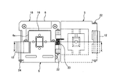
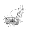
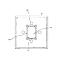
図1は本発明による電気部品用ソケットの実施の形態を示す平面図であり、図2は、図1のX−X線断面図である。この電気部品用ソケットは、ICパッケージのバーンインテスト等の製品検査に使用されるクラムシェルタイプの電気部品用ソケットであり、ソケット本体部18と、コンタクト手段19と、フローティングプレート16と、ソケットカバー5とを備えている。
Hereinafter, embodiments of the present invention will be described in detail with reference to the accompanying drawings.
FIG. 1 is a plan view showing an embodiment of an electrical component socket according to the present invention, and FIG. 2 is a sectional view taken along line XX of FIG. This socket for electrical parts is a clamshell type electrical part socket used for product inspection such as burn-in test of an IC package, and includes a
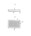
ここで、ICパッケージ3は、図3に示すように、例えば四角形状のパッケージ本体の底面3bに多数の略球形状の半田ボールから成る端子3aが縦列と横列にマトリックス状に配列されたBGA(Ball Grid Array)タイプのものである。
Here, as shown in FIG. 3, the
ソケット本体部18は、図2に示すように、中央部に形成した収容部20にICパッケージ3を収容して保持するものであり、収容部20に対応して四角形の溝部2aを形成し、この溝部2aにシリコーンゴム等の弾性シート9を備えた外形四角形状のベースプレート2と、収容部20に対応して開口部6aを有して略同一の外形形状に形成された中間部材6とを備えて構成する。
As shown in FIG. 2, the
ベースプレート2には、コンタクト手段19が設けられている。このコンタクト手段19は、収容部20に収容されるICパッケージ3の端子3aとベースプレート2の下方に配設される電気回路基板とを電気的に接続するものであり、図2に示すようにコンタクトピン1と、タブフィルム4とで構成する。
Contact means 19 is provided on the
ここで、コンタクトピン1は、導電性を有する金属製板材を例えばプレス加工して形成され、ベースプレート2の周縁部の4辺に沿って多数植設(図2では4列)され、上端部をベースプレート2の上面側に突出してタブフィルム4の接続電極4b(図10参照)と接触する接触部1aとして形成し、下端部をベースプレート2下面側に突出するリード部1bとして形成し、図示省略の電気回路基板のスルーホールにリード部1bを挿入して電気的に接続するようになっている。
Here, the contact pins 1 are formed by, for example, pressing a conductive metal plate material, and a large number of the contact pins 1 are implanted along the four sides of the peripheral portion of the base plate 2 (four rows in FIG. 2). It is formed as a
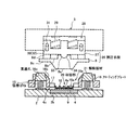
また、タブフィルム4は、例えばポリイミドフィルムに中央部から周縁部に向かってファンアウトする配線を形成した四角形状のフレキシブルプリント基板であり、周縁部の裏面側にはコンタクトピン1の接触部1aと接触する複数の接続電極4b(図10参照)を形成し、中央部の表面には、図4に示すように収容部20に収容されるICパッケージ3の端子3aに接触する複数の接点電極4aを形成し、稠密配列されたICパッケージ3の端子3aとコンタクトピン1との電気的接続を可能にしている。このタブフィルム4は、ベースプレート2中央部に配設された弾性シート9の上に配置され、弾性シート9の弾性力によって、ICパッケージ3の端子3aとタブフィルム4に形成した接点電極4aとの電気的接続を確実に行えるようになっている。また、タブフィルム4には、収容部20の四隅角部に対応して挿入孔4cを形成し、後述のフローティングプレート16の支持部17がフローティングプレート16の下降に伴ってこの挿入孔4cに挿入されるようになっている。
The
さらに、タブフィルム4の上面には、ストッパ10が配設されている。このストッパ10は、ICパッケージ3の端子3aとタブフィルム4の接点電極4aとの位置決めをすると共に、ICパッケージ3の端子3aが高温のバーンインテスト等で変形するのを最小限に抑えるためのものであり、耐熱性、絶縁性及び所定の硬度を有する例えばポリイミド樹脂によって四角形状に形成され、中央部にはICパッケージ3の端子3aを導入する多数の導入孔10aを形成している。そして、ストッパ10の高さは、ICパッケージ3の端子3aの高さよりも僅かに低く形成され、高温テストで端子3aの半田ボールが軟化して変形してもICパッケージ3の底面3bがストッパ10に当接することにより、所定以上に変形が進まないようになっている。
Further, a
また、ベースプレート2の上方部位にて中間部材6の開口部6aには、図1に示すように、フローティングプレート16が収容されている。このフローティングプレート16は、ICパッケージ3を収容部20に案内すると共に、テスト終了後、タブフィルム4の接点電極4aに端子3aが貼りついたICパッケージ3を引き剥がす機能を有するものであり、図5に示すように、収容部20に対応して開口部16aを形成し、この開口部16aの壁面16bを斜面状に形成して(図4参照)ICパッケージ3を収容部20に案内するガイド部とし、この壁面16b下部にて開口部16aの例えば四隅角部には、開口部16aの内側に突出させてICパッケージ3の底面3bに係止する支持部17を形成している。なお、支持部17の高さは、タブフィルム4の厚みとストッパ10の高さとを加算した値に略一致するように形成される。
Further, as shown in FIG. 1, a floating
さらに、開口部16aの各辺の側方中央部には、上下方向に貫通する円錐状の貫通孔16cが形成され、この貫通孔16cには解除部材21が挿入されている。この解除部材21は、後述のパッド8に押圧されて押し下げられフローティングプレート16を上方に付勢する後述の弦巻ばね15の付勢を解除するものであり、貫通孔16cと略等しい円錐台形状を有し、その上端部をフローティングプレート16の上面に突出させている。
Further, a conical through
さらにまた、貫通孔16cに対応したベースプレート2上の部位には、付勢手段としての弦巻ばね15が設けられている。この弦巻ばね15は、フローティングプレート16を弾性的に支持するものであり、一端部をベースプレート2に固定し、他端部を解除部材21の底面に当接して解除部材21を介してフローティングプレート16を付勢するようになっている。
In addition, a
そして、ソケット本体部18の中間部材6の一側端部には、図1又は図2に示すように、ソケットカバー5が回動可能に設けられている。このソケットカバー5は、一側端部を中間部材6の一側端部に回動軸22で回動可能に軸支され、この回動軸22に巻き付けられ、一端部を中間部材6の上面に係止し、他端部をソケットカバー5の内側面に係止させた弦巻ばね23で常時起立方向(開方向)に付勢されている。このソケットカバー5の他端部には、係止手段12が回動軸24により回動可能に軸支されている。この係止手段12は、ソケットカバー5が倒伏して閉じられた際に中間部材6の側面6bに係止してソケットカバー5の閉状態を維持するようにするものであり、回動軸24に巻き付けられ、一端部をソケットカバー5の上面に係止し、他端部を係止手段12の上端内側面に係止させた弦巻ばね25でソケットカバー5の内側に向けて常時付勢されている。そして、ソケットカバー5の収容部20に対向する側の中央部には、押圧手段26が設けられており、ソケットカバー5が閉状態において、この押圧手段26で収容部20に収容されたICパッケージ3の上面を押圧してICパッケージ3の端子3aとコンタクト手段19との電気的接続を確実なものとすることができるようなっている。
As shown in FIG. 1 or 2, the
この押圧手段26は、図4に示すように、プッシャー27とパッド8とで構成されている。プッシャー27は、ソケットカバー5の収容部20に対向する側の面の中央部に形成した凹陥部28に内蔵された弾性部材としての弦巻ばね29で弾性的に支持されて凹陥部28に収容されており、両側端部に縦方向に長い長孔30を形成し、この長孔30に凹陥部28の内側面に支持された2本のシャフト31をそれぞれ挿通して上下動可能にされている。
As shown in FIG. 4, the pressing means 26 includes a
一方、パッド8は、図4において下面8aが上面8bよりも狭い縦断面略逆台形形状に形成され、下面8aでICパッケージ3の上面を押圧するようにしている。また、上面8b側には両側方に突き出した鍔部8cが設けられており、ソケットカバー5の閉動作に伴ってこの鍔部8cが解除部材21に当接して押圧し、解除部材21でフローティングプレート16を付勢する付勢手段15の付勢を解除するようになっている。さらに、パッド8は、その上面8bの両側端部に上方に突出して突出部8dを形成し、この突出部8dにプッシャー27の長孔30に対応して縦方向に長い長孔32を形成し、凹陥部28に設けた2本のシャフト31でプッシャー27と共に上下動可能に保持されている。そして、パッド8は、その上面にプッシャー27の下面中央に形成した半球状の突起33と嵌合する凹部34を設けてプッシャー27に対して揺動可能に保持され、プッシャー27の押圧力をICパッケージ3の上面に均一に作用させることができるようになっている。
On the other hand, the
なお、パッド8は、ソケットカバー5が閉じられて、収容部20に収容されたICパッケージ3が押圧された状態において、フローティングプレート16の貫通孔16c上端面とパッド8の鍔部8cとの間に僅かな隙間が生じるように形成されている(図8参照)。これにより、ICパッケージ3の厚みのバラツキを吸収して弾性手段15の押圧力を確実にICパッケージ3に伝えることができる。
The
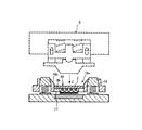
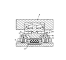
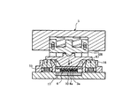
次に、本発明の電気部品用ソケットの動作を、図6〜8を参照して説明する。
先ず、電気部品用ソケットが図示省略の電気回路基板上に配設される。次に、図6に示すように、ソケットカバー5が開状態において、フローティングプレート16の開口部16aに対して矢印C方向にICパッケージ3が落とし込まれる。このICパッケージ3は、開口部16aの壁面16bを斜面状に形成したガイド部によって、開口部16a中央にてベースプレート2中央部の収容部20まで導かれる。このとき、ICパッケージ3は、開口部16aの壁面16b下部の四隅角部に開口部16aの内側に突出させて設けた支持部17にその底面3bを係止されて支持される。
Next, the operation of the electrical component socket of the present invention will be described with reference to FIGS.
First, an electrical component socket is disposed on an electrical circuit board (not shown). Next, as shown in FIG. 6, the
次に、ソケットカバー5を図2において矢印D方向に倒伏させて閉じる。このソケットカバー5の閉動作時には、先ず、図7に示すように、押圧手段26のパッド8の鍔部8cがフローティングプレート16の開口部16aの各辺側方中央部に設けた貫通孔16cに挿入した解除部材21の上端部に当接し、ソケットカバー5の閉動作に伴って、この解除部材21を矢印E方向に押圧し、解除部材21の下面部に配設された弦巻ばね15を押し下げる。これにより、解除部材21の貫通孔16cに対する係止が解除され、フローティングプレート16を上方に付勢する弦巻ばね15の付勢が解除される。したがって、フローティングプレート16は、自重で下降する。また同時にフローティングプレート16の開口部16aに支持部17で支持されたICパッケージ3も下降する。このとき、まだ、パッド8は、ICパッケージ3の上面には当接していない。
Next, the
さらに、ソケットカバー5の閉動作が進んで、図8に示すように、弦巻ばね15が圧縮されてフローティングプレート16が最下点まで下降し、ベースプレート2に接触すると、パッド8がICパッケージ3の上面に当接し、押圧手段26の押圧力FがICパッケージ3に作用する。これにより、ICパッケージ3の端子3aがストッパ10に案内されてタブフィルム4の接点電極4aと接触して電気的接続が確保される。
Further, the closing operation of the
この状態において、ソケットカバー5の係止手段12を中間部材6の側面6bに係止させて(図2参照)ソケットカバー5の閉動作が完了する。そして、ICパッケージ3を収容した電気部品用ソケットは、例えばバーンインテスト等の製品検査に供される。
In this state, the locking means 12 of the
このバーンインテストは、高温の下で実施されるため、ICパッケージ3の端子3aの半田ボールが軟化してタブフィルム4の接点電極4aに貼りつく場合がある。このように貼りついたICパッケージ3は、以下に説明するソケットカバー5の開動作時に容易に引き剥がされる。
Since this burn-in test is performed under a high temperature, the solder ball of the terminal 3 a of the
次に、ソケットカバー5の開動作を説明する。
先ず、ICパッケージ3の製品検査が終了すると、係止手段12による中間部材6の側面6bに対する係止が解除される(図2参照)。これにより、ソケットカバー5は、その側端部に設けた弦巻ばね23の弾性復元力により回動軸22を中心に回動して図2中矢印G方向の開動作を開始する。この開動作により、押圧手段26によるICパッケージ3への押圧力が解除され、図8に示すようにフローティングプレート16が弦巻ばね15の付勢力fにより上方に押し上げられる。同時に、弦巻ばね15の付勢力fは、フローティングプレート16の支持部17を介してICパッケージ3の底面3bに対して上方への引き剥がし力として作用する。この場合、弦巻ばね15の付勢力fがICパッケージ3の貼りつき力よりも十分に大きく設定されていれば、タブフィルム4の接点電極4aに貼りついたICパッケージ3は、この弦巻ばね15の付勢力fにより容易に引き剥がされる。これにより、製品検査後、ICパッケージ3の電気部品用ソケットからの取り出しが容易になる。
Next, the opening operation of the
First, when the product inspection of the
このように、本発明の電気部品用ソケットによれば、ソケットカバー5を閉じる際、ICパッケージ3を押圧する前にフローティングプレート16を弾性的に支持する弦巻ばね15の付勢力を解除するようにしたことにより、ソケットカバー5の閉動作時には、弦巻ばね15の付勢力fがICパッケージ3に作用せず、ICパッケージ3のダメージを抑制することができる。
Thus, according to the electrical component socket of the present invention, when closing the
また、フローティングプレート16に設けた開口部16aの壁部16bに開口部16aの内側に突出させて支持部17を形成し、この支持部17にICパッケージ3を支持するようにしたことにより、ソケットカバー5の開動作時に、フローティングプレート16を支持する弦巻ばね15の付勢力fをICパッケージ3の底面3bに作用させることができる。したがって、バーンインテスト等の高温テストにおいて軟化してタブフィルム4の接点電極4aに貼りついた端子3aを容易に引き剥がすことができる。これにより、テスト後、電気部品用ソケットからICパッケージ3を容易に取り出すことができる。
Further, a
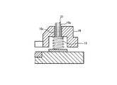
なお、解除部材21は、上述した略円錐台形状のものに限られず、フローティングプレート16の貫通孔16cに係止するブロック状に形成したものであれば如何なる形状であってもよい。また、例えば図9に示すように、弦巻ばね15の上端部に一体的に形成した密巻き部15aを解除部材21とし、この密巻き部15aをフローティングプレート16の貫通孔16cに挿入するようにしてもよい。この場合は、製造が容易になる。
The
さらに、フローティングプレート16を下降させる手段は、フローティングプレート16を上方に付勢する弦巻ばね15の付勢を解除する解除部材21に限られず、押圧手段26によりICパッケージ3が押圧される前にフローティングプレート16を下降させることができれば如何なるものであってもよい。例えば、パッド8の鍔部8c又はソケットカバー5の収容部に対向する側の面にプランジャー等を設け、このプランジャー等でフローティングプレート16を直接押し下げてもよい。
Further, the means for lowering the floating
そして、本発明の電気部品用ソケットは、クラムシェルタイプに限られず、オープントップタイプに適用してもよい。この場合、ソケット本体部18に上下動自在に配設された押圧カバーに連動し、ICパッケージ3を押圧する押圧手段としてのラッチ部材が、ICパッケージ3の上面に当接して押圧する前にフローティングプレート16が下降される構成とするとよい。
And the socket for electrical components of this invention is not restricted to a clamshell type, You may apply to an open top type. In this case, the latch member as a pressing means for pressing the
3…電気部品
3a…端子
5…ソケットカバー
8…パッド
15…弦巻ばね(付勢手段)
16…フローティングプレート
16a…開口部
16b…壁部
16c…貫通孔
17…支持部
18…ソケット本体部
19…コンタクト手段
20…収容部
21…解除部材
26…押圧手段
27…プッシャー
29…弦巻ばね(押圧部材)
3 ...
DESCRIPTION OF
Claims (7)
前記収容部に対して上下動可能に配設され、前記電気部品の底面に係止してこれを支持するフローティングプレートと、
前記ソケット本体部に備えられ、前記フローティングプレートを上方に付勢する付勢手段と、
前記収容部に収容される電気部品に対して、その上面を押圧して電気部品の端子と前記コンタクト手段とを電気的に接続させるように上方から押圧する押圧手段と、
を備えて成る電気部品用ソケットであって、
前記押圧手段が前記電気部品を押圧する際、該電気部品の上面に前記押圧手段が当接して押圧する前に、前記フローティングプレートを下降させる手段を備えたことを特徴とする電気部品用ソケット。 A housing portion formed on the upper surface of the socket body portion, housing electrical components, and provided with contact means capable of contacting the terminals of the electrical components;
A floating plate that is arranged so as to be movable up and down with respect to the housing portion, and that supports and supports the bottom surface of the electrical component;
An urging means provided in the socket main body for urging the floating plate upward;
Press means for pressing from above the electrical component housed in the housing portion so as to press the upper surface thereof to electrically connect the terminal of the electrical component and the contact means;
A socket for electrical parts comprising:
An electrical component socket, comprising: means for lowering the floating plate before the pressing means abuts against and presses the upper surface of the electrical component when the pressing device presses the electrical component.
Priority Applications (1)
| Application Number | Priority Date | Filing Date | Title |
|---|---|---|---|
| JP2004107045A JP4372600B2 (en) | 2004-03-31 | 2004-03-31 | Socket for electrical parts |
Applications Claiming Priority (1)
| Application Number | Priority Date | Filing Date | Title |
|---|---|---|---|
| JP2004107045A JP4372600B2 (en) | 2004-03-31 | 2004-03-31 | Socket for electrical parts |
Publications (2)
| Publication Number | Publication Date |
|---|---|
| JP2005294017A true JP2005294017A (en) | 2005-10-20 |
| JP4372600B2 JP4372600B2 (en) | 2009-11-25 |
Family
ID=35326724
Family Applications (1)
| Application Number | Title | Priority Date | Filing Date |
|---|---|---|---|
| JP2004107045A Expired - Fee Related JP4372600B2 (en) | 2004-03-31 | 2004-03-31 | Socket for electrical parts |
Country Status (1)
| Country | Link |
|---|---|
| JP (1) | JP4372600B2 (en) |
Cited By (9)
| Publication number | Priority date | Publication date | Assignee | Title |
|---|---|---|---|---|
| JP2007109545A (en) * | 2005-10-14 | 2007-04-26 | Japan Aviation Electronics Industry Ltd | socket |
| JP2009158362A (en) * | 2007-12-27 | 2009-07-16 | Enplas Corp | Socket for electric component |
| CN101944701A (en) * | 2010-08-31 | 2011-01-12 | 友达光电(厦门)有限公司 | Connector connection method and connector connection device |
| CN101968499A (en) * | 2009-07-28 | 2011-02-09 | 友达光电(厦门)有限公司 | Connecting method of connector in circuit board test and connecting mechanism thereof |
| JP2015126049A (en) * | 2013-12-26 | 2015-07-06 | 株式会社エンプラス | Heat sink mounting structure and socket for electrical parts |
| WO2016125678A1 (en) * | 2015-02-06 | 2016-08-11 | 株式会社エンプラス | Electric component socket |
| CN114946089A (en) * | 2020-01-21 | 2022-08-26 | 恩普乐股份有限公司 | Socket with improved structure |
| JP2023119925A (en) * | 2022-02-17 | 2023-08-29 | 株式会社エンプラス | Electrical component connection device and inspection device |
| KR20240018201A (en) * | 2022-08-02 | 2024-02-13 | 주식회사 오킨스전자 | Test apparatus for IC |
-
2004
- 2004-03-31 JP JP2004107045A patent/JP4372600B2/en not_active Expired - Fee Related
Cited By (15)
| Publication number | Priority date | Publication date | Assignee | Title |
|---|---|---|---|---|
| JP2007109545A (en) * | 2005-10-14 | 2007-04-26 | Japan Aviation Electronics Industry Ltd | socket |
| JP2009158362A (en) * | 2007-12-27 | 2009-07-16 | Enplas Corp | Socket for electric component |
| CN101968499A (en) * | 2009-07-28 | 2011-02-09 | 友达光电(厦门)有限公司 | Connecting method of connector in circuit board test and connecting mechanism thereof |
| CN101944701A (en) * | 2010-08-31 | 2011-01-12 | 友达光电(厦门)有限公司 | Connector connection method and connector connection device |
| JP2015126049A (en) * | 2013-12-26 | 2015-07-06 | 株式会社エンプラス | Heat sink mounting structure and socket for electrical parts |
| JP2016145710A (en) * | 2015-02-06 | 2016-08-12 | 株式会社エンプラス | Socket for electrical parts |
| WO2016125678A1 (en) * | 2015-02-06 | 2016-08-11 | 株式会社エンプラス | Electric component socket |
| CN107889560A (en) * | 2015-02-06 | 2018-04-06 | 恩普乐股份有限公司 | Socket for electronic component |
| US10274535B2 (en) | 2015-02-06 | 2019-04-30 | Enplas Corporation | Electric component socket |
| CN107889560B (en) * | 2015-02-06 | 2020-03-10 | 恩普乐股份有限公司 | Sockets for electronic components |
| CN114946089A (en) * | 2020-01-21 | 2022-08-26 | 恩普乐股份有限公司 | Socket with improved structure |
| JP2023119925A (en) * | 2022-02-17 | 2023-08-29 | 株式会社エンプラス | Electrical component connection device and inspection device |
| JP7766515B2 (en) | 2022-02-17 | 2025-11-10 | 株式会社エンプラス | Electrical component connection device and inspection device |
| KR20240018201A (en) * | 2022-08-02 | 2024-02-13 | 주식회사 오킨스전자 | Test apparatus for IC |
| KR102788961B1 (en) | 2022-08-02 | 2025-04-01 | 주식회사 오킨스전자 | Test apparatus for IC |
Also Published As
| Publication number | Publication date |
|---|---|
| JP4372600B2 (en) | 2009-11-25 |
Similar Documents
| Publication | Publication Date | Title |
|---|---|---|
| JP4133141B2 (en) | Socket for electrical parts | |
| JP6411546B2 (en) | Socket device for semiconductor device test | |
| JP5196327B2 (en) | Socket for semiconductor device | |
| US7393232B2 (en) | Socket for electrical parts | |
| KR102520051B1 (en) | Test socket and Method for testing semiconductor package | |
| JP2012089389A (en) | Socket for electrical component | |
| JPH07240263A (en) | Burn-in receptacle | |
| JP4372600B2 (en) | Socket for electrical parts | |
| US7097488B2 (en) | Socket for electrical parts | |
| JPH09289068A (en) | Ic socket | |
| JPH0850975A (en) | Ball grid array device mounting device | |
| KR101245838B1 (en) | Socket device for testing a thin film ic package having an anti-warpage means | |
| JP2006127936A (en) | Socket for electric component | |
| JP2004079227A (en) | IC socket | |
| JP2005294018A (en) | Socket for electric component | |
| JP2000183483A (en) | Inspection board for electronic component, method for manufacturing the same, and method for inspecting electronic component | |
| US6544044B2 (en) | Socket for BGA package | |
| JP4187281B2 (en) | IC socket for testing | |
| US7407401B2 (en) | Socket for electrical parts | |
| JP4550642B2 (en) | Socket for electrical parts | |
| JP2005134373A (en) | Connection device using spiral contactor | |
| JP2003297512A (en) | Socket for electric component | |
| JP2005174670A (en) | Open top IC socket | |
| JP4786414B2 (en) | Socket for electrical parts | |
| JP4169841B2 (en) | Socket for electrical parts |
Legal Events
| Date | Code | Title | Description |
|---|---|---|---|
| A621 | Written request for application examination |
Effective date: 20070314 Free format text: JAPANESE INTERMEDIATE CODE: A621 |
|
| A977 | Report on retrieval |
Free format text: JAPANESE INTERMEDIATE CODE: A971007 Effective date: 20090522 |
|
| A131 | Notification of reasons for refusal |
Free format text: JAPANESE INTERMEDIATE CODE: A131 Effective date: 20090602 |
|
| A521 | Written amendment |
Effective date: 20090731 Free format text: JAPANESE INTERMEDIATE CODE: A523 |
|
| TRDD | Decision of grant or rejection written | ||
| A01 | Written decision to grant a patent or to grant a registration (utility model) |
Free format text: JAPANESE INTERMEDIATE CODE: A01 Effective date: 20090901 |
|
| A01 | Written decision to grant a patent or to grant a registration (utility model) |
Free format text: JAPANESE INTERMEDIATE CODE: A01 |
|
| A61 | First payment of annual fees (during grant procedure) |
Free format text: JAPANESE INTERMEDIATE CODE: A61 Effective date: 20090902 |
|
| FPAY | Renewal fee payment (prs date is renewal date of database) |
Year of fee payment: 3 Free format text: PAYMENT UNTIL: 20120911 |
|
| R150 | Certificate of patent (=grant) or registration of utility model |
Free format text: JAPANESE INTERMEDIATE CODE: R150 |
|
| FPAY | Renewal fee payment (prs date is renewal date of database) |
Free format text: PAYMENT UNTIL: 20120911 Year of fee payment: 3 |
|
| FPAY | Renewal fee payment (prs date is renewal date of database) |
Free format text: PAYMENT UNTIL: 20120911 Year of fee payment: 3 |
|
| FPAY | Renewal fee payment (prs date is renewal date of database) |
Year of fee payment: 3 Free format text: PAYMENT UNTIL: 20120911 |
|
| FPAY | Renewal fee payment (prs date is renewal date of database) |
Year of fee payment: 4 Free format text: PAYMENT UNTIL: 20130911 |
|
| LAPS | Cancellation because of no payment of annual fees |