JP2005293975A - 接続端子 - Google Patents
接続端子 Download PDFInfo
- Publication number
- JP2005293975A JP2005293975A JP2004105998A JP2004105998A JP2005293975A JP 2005293975 A JP2005293975 A JP 2005293975A JP 2004105998 A JP2004105998 A JP 2004105998A JP 2004105998 A JP2004105998 A JP 2004105998A JP 2005293975 A JP2005293975 A JP 2005293975A
- Authority
- JP
- Japan
- Prior art keywords
- terminal
- connection
- circuit
- foil
- circuit board
- Prior art date
- Legal status (The legal status is an assumption and is not a legal conclusion. Google has not performed a legal analysis and makes no representation as to the accuracy of the status listed.)
- Granted
Links
Images


Landscapes
- Multi-Conductor Connections (AREA)
- Coupling Device And Connection With Printed Circuit (AREA)
- Connection Or Junction Boxes (AREA)
Abstract
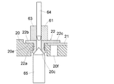
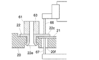
【解決手段】 受端子22は例えば肉厚0.2mmの黄銅板から成り、フォーミングプレスにより形成され、短円筒状に形成した筒状接続部22aの上部にフランジ部22bが形成され、更にフランジ部22bの一部にタブ22cが付設されている。筒状接続部22aとフランジ部22bとの境界部は、挿入端子を受け入れるためのテーパ状の案内部22dとされている。
【選択図】図6
Description
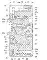
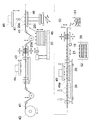
図1は本発明に係る接続端子である受端子を使用するジョイントボックスの分解斜視図であり、上ケース11、回路ユニット12、下ケース13を相互に組み付けることにより、ボックス形状のジョイントボックスが得られる。つまり、上ケース11、下ケース13間に回路ユニット12が収納され、ケース11、13同士が接合されると、回路ユニット12を収容した状態で上ケース11、下ケース13に設けられたロック部14a、14bによりロックされる。
12 回路ユニット
13 下ケース
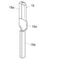
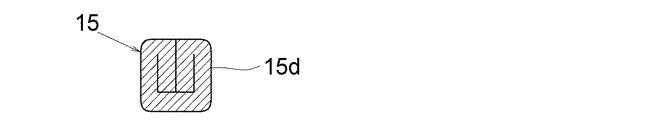
15 挿入端子
15d 挿入端
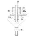
16 ブロック体
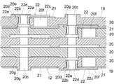
19 回路基板
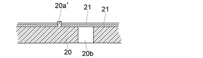
20 樹脂プレート
20c 端子挿通孔
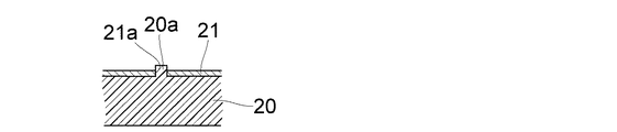
21 箔回路
22 受端子
Claims (6)
- 1枚の金属板を打ち抜き折曲して形成しピン状端子の挿入端を受け入れる受型の接続端子であって、前記挿入端を受け入れる短円筒状の筒状接続部と、該筒状接続部の上部周囲に設けたフランジ部と、該フランジ部の一部から延出した導体接続部とを備えたことを特徴とする接続端子。
- 前記筒状接続部とフランジ部との境界部はテーパ状とし、前記挿入端の案内部としたことを特徴とする請求項1に記載の接続端子。
- 前記導体接続部はタブとし、該タブを導体と溶着又は半田付けすることを特徴とする請求項1に記載の接続端子。
- 前記導体接続部は圧着端子としたことを特徴とする請求項1に記載の接続端子。
- 前記筒状接続部を支持用絶縁部材の孔部に挿入し、前記筒状接続部の下部を拡開して前記絶縁部材にかしめ止めしたことを特徴とする請求項1に記載の接続端子。
- 前記拡開した筒状接続部の下部は、下方からの前記挿入端の案内部としたことを特徴とする請求項5に記載の接続端子。
Priority Applications (1)
| Application Number | Priority Date | Filing Date | Title |
|---|---|---|---|
| JP2004105998A JP4578843B2 (ja) | 2004-03-31 | 2004-03-31 | 回路基板用接続端子 |
Applications Claiming Priority (1)
| Application Number | Priority Date | Filing Date | Title |
|---|---|---|---|
| JP2004105998A JP4578843B2 (ja) | 2004-03-31 | 2004-03-31 | 回路基板用接続端子 |
Related Child Applications (1)
| Application Number | Title | Priority Date | Filing Date |
|---|---|---|---|
| JP2010155846A Division JP4939634B2 (ja) | 2010-07-08 | 2010-07-08 | 回路基板用接続端子 |
Publications (2)
| Publication Number | Publication Date |
|---|---|
| JP2005293975A true JP2005293975A (ja) | 2005-10-20 |
| JP4578843B2 JP4578843B2 (ja) | 2010-11-10 |
Family
ID=35326691
Family Applications (1)
| Application Number | Title | Priority Date | Filing Date |
|---|---|---|---|
| JP2004105998A Expired - Fee Related JP4578843B2 (ja) | 2004-03-31 | 2004-03-31 | 回路基板用接続端子 |
Country Status (1)
| Country | Link |
|---|---|
| JP (1) | JP4578843B2 (ja) |
Cited By (1)
| Publication number | Priority date | Publication date | Assignee | Title |
|---|---|---|---|---|
| JP2010219072A (ja) * | 2010-07-08 | 2010-09-30 | Mitsubishi Cable Ind Ltd | 回路基板用接続端子 |
Citations (4)
| Publication number | Priority date | Publication date | Assignee | Title |
|---|---|---|---|---|
| JPS5246291U (ja) * | 1975-09-29 | 1977-04-01 | ||
| JPS5350465U (ja) * | 1976-10-01 | 1978-04-28 | ||
| JPH08222825A (ja) * | 1995-02-13 | 1996-08-30 | Nec Corp | プリント基板の接続構造 |
| JPH08306418A (ja) * | 1995-03-08 | 1996-11-22 | Alps Electric Co Ltd | コネクタのピンコンタクトおよびその製造方法 |
-
2004
- 2004-03-31 JP JP2004105998A patent/JP4578843B2/ja not_active Expired - Fee Related
Patent Citations (4)
| Publication number | Priority date | Publication date | Assignee | Title |
|---|---|---|---|---|
| JPS5246291U (ja) * | 1975-09-29 | 1977-04-01 | ||
| JPS5350465U (ja) * | 1976-10-01 | 1978-04-28 | ||
| JPH08222825A (ja) * | 1995-02-13 | 1996-08-30 | Nec Corp | プリント基板の接続構造 |
| JPH08306418A (ja) * | 1995-03-08 | 1996-11-22 | Alps Electric Co Ltd | コネクタのピンコンタクトおよびその製造方法 |
Cited By (1)
| Publication number | Priority date | Publication date | Assignee | Title |
|---|---|---|---|---|
| JP2010219072A (ja) * | 2010-07-08 | 2010-09-30 | Mitsubishi Cable Ind Ltd | 回路基板用接続端子 |
Also Published As
| Publication number | Publication date |
|---|---|
| JP4578843B2 (ja) | 2010-11-10 |
Similar Documents
| Publication | Publication Date | Title |
|---|---|---|
| JP4719759B2 (ja) | 回路基板の製造方法 | |
| JP6966046B2 (ja) | バッテリーモジュール用fpcb組立体、その製造方法及びそれを含むバッテリーモジュール | |
| US5434749A (en) | Hybrid printed circuit board | |
| CN102640355A (zh) | 具有焊料构件的电触头以及将焊料构件安装到电触头的方法 | |
| EP2679080B1 (en) | A connection pin for mounting in a component carrier, a method for producing an electronic assembly comprising a motherboard with stackable modules comprising a component carrier, and such an electronic assembly | |
| US20100186997A1 (en) | Crimped solder on a flexible circuit board | |
| JP4939634B2 (ja) | 回路基板用接続端子 | |
| JP4578843B2 (ja) | 回路基板用接続端子 | |
| JPH0634446B2 (ja) | 回路基板のはんだ付方法 | |
| EP0312607A1 (en) | Power circuit board and manufacturing method | |
| US20110266043A1 (en) | Substrate | |
| US6725537B2 (en) | Method of connecting circuit element | |
| JP5601828B2 (ja) | プリント配線基板積層体およびその製造方法 | |
| JP3303801B2 (ja) | 回路板、該回路板を備えた電気接続箱および回路板の製造方法 | |
| KR20110033932A (ko) | 회로 구조체, 조인트박스 및 회로 구조체의 제조방법 | |
| JPH0550708U (ja) | シートコイル装置 | |
| JP2009267050A (ja) | 接続ピン、機能モジュール、および機能モジュールのマウント方法 | |
| JPH07249528A (ja) | プレーナ型磁性部品 | |
| US20090239419A1 (en) | Connector header with wire wrap pins | |
| JP2007166743A (ja) | 電気接続箱 | |
| JP2004159432A (ja) | 電子部品内蔵の電気接続箱 | |
| JP2006134920A (ja) | 積層部品及び積層部品の実装構造 |
Legal Events
| Date | Code | Title | Description |
|---|---|---|---|
| A711 | Notification of change in applicant |
Free format text: JAPANESE INTERMEDIATE CODE: A712 Effective date: 20060317 |
|
| A621 | Written request for application examination |
Free format text: JAPANESE INTERMEDIATE CODE: A621 Effective date: 20070221 |
|
| A977 | Report on retrieval |
Free format text: JAPANESE INTERMEDIATE CODE: A971007 Effective date: 20090416 |
|
| A131 | Notification of reasons for refusal |
Free format text: JAPANESE INTERMEDIATE CODE: A131 Effective date: 20090428 |
|
| A521 | Written amendment |
Free format text: JAPANESE INTERMEDIATE CODE: A523 Effective date: 20090622 |
|
| A02 | Decision of refusal |
Free format text: JAPANESE INTERMEDIATE CODE: A02 Effective date: 20091215 |
|
| A521 | Written amendment |
Free format text: JAPANESE INTERMEDIATE CODE: A523 Effective date: 20100308 |
|
| A911 | Transfer of reconsideration by examiner before appeal (zenchi) |
Free format text: JAPANESE INTERMEDIATE CODE: A911 Effective date: 20100323 |
|
| A131 | Notification of reasons for refusal |
Free format text: JAPANESE INTERMEDIATE CODE: A131 Effective date: 20100622 |
|
| A521 | Written amendment |
Free format text: JAPANESE INTERMEDIATE CODE: A523 Effective date: 20100708 |
|
| TRDD | Decision of grant or rejection written | ||
| A01 | Written decision to grant a patent or to grant a registration (utility model) |
Free format text: JAPANESE INTERMEDIATE CODE: A01 Effective date: 20100803 |
|
| A01 | Written decision to grant a patent or to grant a registration (utility model) |
Free format text: JAPANESE INTERMEDIATE CODE: A01 |
|
| A61 | First payment of annual fees (during grant procedure) |
Free format text: JAPANESE INTERMEDIATE CODE: A61 Effective date: 20100825 |
|
| FPAY | Renewal fee payment (event date is renewal date of database) |
Free format text: PAYMENT UNTIL: 20130903 Year of fee payment: 3 |
|
| R150 | Certificate of patent or registration of utility model |
Free format text: JAPANESE INTERMEDIATE CODE: R150 |
|
| FPAY | Renewal fee payment (event date is renewal date of database) |
Free format text: PAYMENT UNTIL: 20130903 Year of fee payment: 3 |
|
| S111 | Request for change of ownership or part of ownership |
Free format text: JAPANESE INTERMEDIATE CODE: R313113 |
|
| FPAY | Renewal fee payment (event date is renewal date of database) |
Free format text: PAYMENT UNTIL: 20130903 Year of fee payment: 3 |
|
| R350 | Written notification of registration of transfer |
Free format text: JAPANESE INTERMEDIATE CODE: R350 |
|
| R250 | Receipt of annual fees |
Free format text: JAPANESE INTERMEDIATE CODE: R250 |
|
| LAPS | Cancellation because of no payment of annual fees |