JP2005293751A - Semiconductor memory - Google Patents
Semiconductor memory Download PDFInfo
- Publication number
- JP2005293751A JP2005293751A JP2004109059A JP2004109059A JP2005293751A JP 2005293751 A JP2005293751 A JP 2005293751A JP 2004109059 A JP2004109059 A JP 2004109059A JP 2004109059 A JP2004109059 A JP 2004109059A JP 2005293751 A JP2005293751 A JP 2005293751A
- Authority
- JP
- Japan
- Prior art keywords
- pair
- power supply
- semiconductor memory
- pseudo
- memory cell
- Prior art date
- Legal status (The legal status is an assumption and is not a legal conclusion. Google has not performed a legal analysis and makes no representation as to the accuracy of the status listed.)
- Pending
Links
Images
Landscapes
- Static Random-Access Memory (AREA)
Abstract
Description
本発明は、極微細LSI製造プロセスを用いた半導体メモリに関するものであり、特に高速なスタティツク形ランダムアクセスメモリ(Static Random Access Memory;SRAM)に適用して有効な低消費電力化技術に関する。 The present invention relates to a semiconductor memory using an ultrafine LSI manufacturing process, and particularly to a low power consumption technique effective when applied to a high-speed static random access memory (SRAM).
上記の技術分野に属する従来の半導体メモリとして、例えば、特許文献1に記載のものがある。図10はその特許文献1に記載された半導体メモリの回路図である。以下の説明において、特に断らない限り、High状態とはVDDもしくはVDD近傍の高レベルのことであり、Low状態とはGNDもしくはGND近傍の低レベルのことを示す。
As a conventional semiconductor memory belonging to the above technical field, for example, there is one described in
メモリセル10は、フリップフロップ回路を構成する一対の負荷用pMOSFETQ1,Q2と一対の駆動用nMOSFETQ3,Q4に、セル選択用のnMOSトランスファゲートQ5,Q6を組み合わせて構成される。フリップフロップ回路の一対の回路節点N1,N2は何れか一方がHighレベル状態、他方がLowレベル状態となり、その状態の違いによってメモリセル10は1ビットのデータを記憶する。WLはワード線、BL,/BLは対となるビット線、VG,/VGは対となる擬似GND線である。
The
ワード線WLはメモリセル10の選択信号を伝送する線路であり、非選択状態でGNDレベル、選択状態でVDDレベルに制御される。一対のビット線BL,/BLは、書込み時に入力データに対応した電圧信号を差動信号の形態で当該メモリセル10まで伝送する線路である。このビット線BL,/BLは、非書込み期間中は共にVDDもしくはVDD近傍の高レベルに制御されており、メモリセル10にデータを書き込む時のみ、入力データに応じて何れか一方のビット線だけがGNDもしくはGND近傍の低レベルに制御される。一対の擬似GND線VG,/VGは、読出し時にメモリセル10の記憶内容に応じた電流信号を差動信号の形態で電流センス回路5まで伝送する線路である。擬似GND線VG,/VGのレベルは、GNDもしくはGND近傍の低レベルである。
The word line WL is a line for transmitting a selection signal of the
なお、通常は複数のワード線と複数のビット線ペア(および擬似GND線ペア)を用意し、それらの交点にメモリセル10を配置してメモリセルアレイが構成される。図10では説明図の煩雑さを避ける意味で、着目しているワード線、ビット線ペア、擬似GND線ペア、そしてメモリセルだけを図示し、その他のワード線、ビット線ペア、擬似GND線ペア、メモリセルについては省略している。
Usually, a plurality of word lines and a plurality of bit line pairs (and pseudo GND line pairs) are prepared, and
図10において、DI、Y、WE、SAEは入力端子、DOは出力端子である。入力端子DIには入力データDI、入力端子Yには当該ビット線ペアに対応したコラム選択信号Y、入力端子WEには書込要求信号WE、入力端子SAEには当該擬似GND線ペアに対応した電流センス回路活性化信号SAEを入力する。出力端子DOからは読出しデータDOが出力される。これらの入力信号又は出力信号は、何れも2値の電圧信号(VDD又はGNDレベル)である。その他、図10では省略しているが、半導体メモリの入力信号のひとつにチップ選択信号CSがある。チップ選択信号CSは半導体メモリをスタンバイ状態もしくは動作状態に切り替える特別な制御信号である。データの読出し又は書込みを行う際は、当該半導体メモリを事前に動作状態に制御する必要があるが、以下で述べる読出し動作もしくは書込み動作に直接関与しないので、記述を省略する。 In FIG. 10, DI, Y, WE, and SAE are input terminals, and DO is an output terminal. The input terminal DI corresponds to the input data DI, the input terminal Y corresponds to the column selection signal Y corresponding to the bit line pair, the input terminal WE corresponds to the write request signal WE, and the input terminal SAE corresponds to the pseudo GND line pair. Current sense circuit activation signal SAE is input. Read data DO is output from the output terminal DO. These input signals or output signals are all binary voltage signals (VDD or GND level). In addition, although omitted in FIG. 10, a chip selection signal CS is one of input signals of the semiconductor memory. The chip selection signal CS is a special control signal for switching the semiconductor memory to a standby state or an operating state. When reading or writing data, it is necessary to control the semiconductor memory in an operating state in advance, but the description is omitted because it is not directly related to the reading or writing operation described below.
図10の構成要素の内、1’は入力データDIの書込み動作を制御する書込制御回路、2’はビット線BL,/BLをドライブする反転形の一対の書込みバッファであり、これらで書込み回路を構成している。データの非書込み時は、書込みバッファ2’はビット線BL,/BLをVDDもしくはVDD近傍のHighレベルにプルアップする。3’は固定電源であり、メモリセル10に電圧VDDを供給する。4は擬似的に定電流源として機能する高抵抗、5は電流センス回路であり、これらで読出し回路を構成している。電流センス回路5は、入力端子から流出する電流(IS1,IS2)の大小比較を行い、その結果を2値の電圧信号(VDD又はGNDレベル)の形態で出力端子DOに出力する。
10, 1 'is a write control circuit for controlling the write operation of the input data DI, and 2' is a pair of inverted write buffers for driving the bit lines BL and / BL. The circuit is configured. When data is not written, the write buffer 2 'pulls up the bit lines BL and / BL to VDD or a high level near VDD.
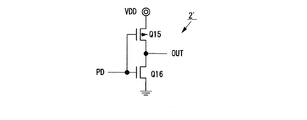
図11は図10における反転型の書込みバッファ2’の回路図である。この書込みバッファ2’はpMOSFETQ15とnMOSFETQ16より構成されるインバータからなり、入力端子PDがHigh状態(VDDレベル)のとき出力端子OUTはGNDレベルである。逆に、入力端子PDがLow状態(GNDレベル)のとき出力端子OUTはVDDレベルである。 FIG. 11 is a circuit diagram of the inverting write buffer 2 'in FIG. The write buffer 2 'is composed of an inverter composed of a pMOSFET Q15 and an nMOSFET Q16. When the input terminal PD is in a high state (VDD level), the output terminal OUT is at the GND level. Conversely, when the input terminal PD is in the low state (GND level), the output terminal OUT is at the VDD level.
半導体メモリに対して、データを書き込む又は読み出す操作を以下に概説する。図10のメモリセル10にはデータ“1”が記憶されており、回路節点N1はHighレベル状態、N2はLowレベル状態にあるとする。
An operation for writing or reading data to or from a semiconductor memory will be outlined below. It is assumed that data “1” is stored in the
<読み出し動作>
図10の従来例において、メモリセル10に記憶されたデータ“1”を出力端子DOに読み出す動作は以下の通りである。読出し動作を通じて、書込要求信号WEは非書込み状態(GNDレベル)である。
<Read operation>
In the conventional example of FIG. 10, the operation of reading the data “1” stored in the
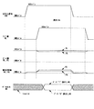
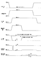
図12は図10の半導体メモリの主要な回路節点の動作波形である。一連の読出し動作の初期状態として、活性化信号SAEは非活性状態(GNDレベル)とする。ワード線WLは非選択状態(GNDレベル)、ビット線BL,/BLはVDDレベル、擬似GND線VG,/VGはGNDレベルである。メモリセル10内のMOSFETに関しては、Q1,Q4は導通状態、Q2,Q3,Q5,Q6は非導通状態である。
FIG. 12 shows operation waveforms at main circuit nodes of the semiconductor memory of FIG. As an initial state of a series of read operations, the activation signal SAE is in an inactive state (GND level). The word line WL is in a non-selected state (GND level), the bit lines BL and / BL are at VDD level, and the pseudo GND lines VG and / VG are at GND level. Regarding the MOSFET in the
読出し動作は、当該コラムの活性化信号SAEをVDDレベルに制御して、電流センス回路5を活性状態にすることから始まる。その際、電流センス回路5から擬似GND線VG,/VGに定常的に流出する電流によって高抵抗4の両端に逆起電力が発生し、擬似GND線VG,/VGのレベルがGNDからGND近傍の低レベルまで上昇する。しかる後、ワード線WLを選択状態(VDDレベル)に制御する。このとき、記憶内容を反映してMOSFETQ6が導通し、ビット線/BLから擬似GND線VGへの電流経路が形成される。MOSFETQ5については非導通状態を維持するので、対となるビット線BLから擬似GND線/VGへの電流経路は形成されない。メモリセル10から擬似GND線へ流出した読出し電流は、定電流源として機能する高抵抗4で折り返されて、電流センス回路5に入力される。議論を簡単にする為に、高抵抗4を理想定電流源と見なすと、メモリセル10から擬似GND線/VG,VGへ流出する読出し電流IR1,IR2と電流センス回路5から流出する電流IS1,IS2には、以下の関係がある。
IR1+IS1=IR2+IS2
上述の例では、「IR2>0かつIR1=0」であるので、電流センス回路5の入力信号には「IS1>IS2>0」の関係がある。これを電流センス回路5は検出して、データ“1”に相当するVDDレベルの信号を出力端子DOから出力する。
The read operation starts by controlling the activation signal SAE for the column to the VDD level to activate the
IR1 + IS1 = IR2 + IS2
In the above example, since “IR2> 0 and IR1 = 0”, the input signal of the
一方、メモリセル10にデータ“0”が記憶されている場合は、回路節点N1がLow状態、N2がHigh状態になるので、電流センス回路5はデータ“0”に相当するGNDレベルの信号を出力端子DOから出力する。
On the other hand, when data “0” is stored in the
図10では省略されているが、ビット線ペアが複数ある場合は、出力端子DOからの読出しデータDOを多重化して外部へ出力する為のマルチプレクサが電流センス回路5の後段に設けられる。その際、非選択コラムについては、電流センス回路5が活性化されないので、ワード線WLが選択されてもデータは読み出されない。
Although omitted in FIG. 10, when there are a plurality of bit line pairs, a multiplexer for multiplexing the read data DO from the output terminal DO and outputting it to the outside is provided at the subsequent stage of the
<書込み動作>
データ“1”が記憶された図10のメモリセル10に、入力端子DIから入力された逆データ“0”を書き込む動作について以下に述べる。書込み動作を通じて、活性化信号SAEは非活性状態(GNDレベル)である。
<Write operation>
The operation of writing the reverse data “0” input from the input terminal DI into the
図13は図10の半導体メモリの主要な回路節点の動作波形である。一連の書込み動作の初期状態として、コラム選択信号Yは非選択状態(Lowレベル)、ワード線WLは非選択状態(GNDレベル)、書込要求信号WEは非書込み状態(GNDレベル)とする。ビット線BL側の書込みバッファ2’の入力とビット線/BL側の書込みバッファ2’の入力は共にLowレベルであり、ビット線BL,/BLは共にVDDレベルに設定されている。擬似GND線VG,/VGはGNDレベルである。メモリセル10内のMOSFETに関しては、Q1,Q4は導通状態、Q2,Q3,Q5,Q6は非導通状態である。
FIG. 13 shows operation waveforms at main circuit nodes of the semiconductor memory of FIG. As an initial state of a series of write operations, the column selection signal Y is in a non-selection state (Low level), the word line WL is in a non-selection state (GND level), and the write request signal WE is in a non-write state (GND level). Both the input of the
入力端子DIに入力されたデータ“0”の書込み動作は、入力端子Yの当該コラム選択信号Yを選択状態(VDDレベル)にして、ビット線ペアを特定することから始まる。しかる後、ワード線WLを選択状態(VDDレベル)、書込要求信号WEを書込み状態(VDDレベル)に制御する。その際、書込制御回路1’の動作により、ビット線BL側の書込みバッファ2’の入力がHighレベル状態に制御されるので、ビット線BLはGNDレベルにドライブされる。ビット線/BL側の書込みバッファ2’については、その入力はLowレベル状態から変化しないので、ビット線/BLはVDDレベルを維持する。ビット線BLの電位の低下と共に、MOSFETQ5のゲート・ソース(ビット線BL側のMOSFET節点)間にはMOSFETの閾値電圧を超える十分大きな電圧が印加されることになり、MOSFETQ5は導通状態になる。その結果、回路節点N1の電位は低下し、MOSFETQ2,Q4で構成されるインバータの論埋閾値を下回ると、フリップフロップ回路の状態は反転し、回路節点N1がLowレベル状態、回路節点N2がHighレベル状態に変化して、メモリセル10は更新データを保持可能になる。しかる後、書込要求信号WEを非書込み状態(GNDレベル)に制御し、それに続いてワード線WLを非選択状態(GNDレベル)に復帰させる。書込要求信号WEを非書込み状態に制御することにより、書込制御回路1’はビット線BL側および/BL側の書込みバッファ2’の入力を共にLowレベルに制御するので、書込みバッファ2’の動作により、ビット線BLは初期のVDDレベルまで回復する。書込要求信号WEを非書込み状態(Lowレベル)に制御するタイミングは、メモリセル10内のフリップフロップ回路の状態が反転した後であれば、特に制約はない。入力データDI、コラム選択信号Y、ワード線WLに関しては、ビット線BLが初期のレベルに回復した後であれは、状態を変化させるタイミングに特に制約はない。
The write operation of the data “0” input to the input terminal DI starts by setting the column selection signal Y of the input terminal Y to the selected state (VDD level) and specifying the bit line pair. Thereafter, the word line WL is controlled to the selected state (VDD level), and the write request signal WE is controlled to the write state (VDD level). At this time, the input of the
なお、非選択コラムのビット線については、書込み動作を通じて、ビット線BL側も/BL側も書込みバッファ2’によってVDD又はその近傍の高レベルにプルアップされている。
Note that the bit lines of the non-selected columns are pulled up to VDD or a high level in the vicinity thereof by the
ところで、半導体メモリの動作速度と消費電力、そして使用するMOSFETのゲート長には密接な関係がある。ゲート長の短いMOSFETを利用可能な極微細LSI製造プロセスを適用することは、半導体メモリの動作速度を改善する有効な手段ではあるが、同時にMOSFETのサブスレッショルドリーク電流の増大を招く。サブスレッショルドリーク電流とは、オフ状態のMOSFETに流れるゲート・ソース間のリーク電流のことであり、スタンバイ状態/動作状態の別なく、半導体メモリの消費電力増の原因になる。その為、大規模な半導体メモリでは、高速化手段としての極微細LSIプロセスの適用が制限されてしまうという問題があった。 By the way, there is a close relationship between the operation speed and power consumption of the semiconductor memory and the gate length of the MOSFET to be used. Applying a very fine LSI manufacturing process that can use a MOSFET having a short gate length is an effective means for improving the operation speed of the semiconductor memory, but at the same time, increases the subthreshold leakage current of the MOSFET. The subthreshold leakage current is a leakage current between the gate and the source that flows through the MOSFET in the off state, and causes an increase in power consumption of the semiconductor memory regardless of whether it is in the standby state / operating state. For this reason, there has been a problem that the application of the ultra fine LSI process as a speed-up means is limited in a large-scale semiconductor memory.
また、サブスレッショルドリーク電流にはゲート長の他に、ソース・ドレイン間に印加される電圧にも依存する性質があるので、電源電圧を下げることである程度低減可能である。しかし、電源電圧を下げると、オン状態のMOSFETのゲート・ソース間に印加される電圧が低下する為に、MOSFETのオン電流(ドレイン電流)が減少し、ディジタル回路、アナログ回路を問わず遅延時間は増大する。これは、半導体メモリの動作速度の低下に繋がるので、動作電圧の低電圧化だけでは解決できないという問題があった。 Further, since the subthreshold leakage current has a property that depends on the voltage applied between the source and drain in addition to the gate length, it can be reduced to some extent by lowering the power supply voltage. However, when the power supply voltage is lowered, the voltage applied between the gate and source of the MOSFET in the on state is lowered, so that the on-current (drain current) of the MOSFET is reduced and the delay time regardless of whether it is a digital circuit or an analog circuit. Will increase. This leads to a decrease in the operating speed of the semiconductor memory, and there is a problem that it cannot be solved only by reducing the operating voltage.
本発明の目的は、上述の問題点を解決するべく、極微細LSI製造プロセスを適用して有効な、動作速度の低下のない、低消費電力な半導体メモリを提供することにある。 SUMMARY OF THE INVENTION An object of the present invention is to provide a low-power-consumption semiconductor memory that is effective by applying an ultrafine LSI manufacturing process and does not decrease the operation speed in order to solve the above-mentioned problems.
請求項1にかかる発明は、一対の負荷用MOSFETおよび一対の駆動用MOSFETからなるフリップフロップ回路並びに該フリップフロップ回路の一方と他方の入出力側にそれぞれ接続した一対のセル選択用MOSFETからなるメモリセルと、前記一対のセル選択用MOSFETの前記フリップフロップ回路に接続される側と反対のドレイン又はソースにそれぞれ接続した一対のビット線と、前記一対の負荷用MOSFETのソースに共通接続した擬似電源線と、前記一対の駆動用MOSFETのソースにそれぞれ接続した一対の擬似GND線と、前記一対のビット線にそれぞれ接続した一対の書込みバッファと、前記一対の擬似GND線に共通接続した電流センス回路とを有する半導体メモリにおいて、出力電圧が異なる第1および第2の電源と、前記各書込みバッファのHigh出力レベルを前記第1又は第2の電源の電圧に対応する電圧に個々に切り替える手段と、前記擬似電源線のレベルを前記第1又は第2電源の電圧に対応する電圧に切り替える手段を設けたことを特徴とする。 According to the first aspect of the present invention, there is provided a flip-flop circuit comprising a pair of load MOSFETs and a pair of drive MOSFETs, and a memory comprising a pair of cell selection MOSFETs respectively connected to one input / output side of the flip-flop circuit. A pseudo power supply commonly connected to a cell, a pair of bit lines connected to the drain or source opposite to the side connected to the flip-flop circuit of the pair of cell selection MOSFETs, and a source of the pair of load MOSFETs A pair of pseudo GND lines connected to the sources of the pair of driving MOSFETs, a pair of write buffers connected to the pair of bit lines, and a current sensing circuit commonly connected to the pair of pseudo GND lines, respectively. In the semiconductor memory having the first and the different output voltages Two power supplies, means for individually switching the High output level of each write buffer to a voltage corresponding to the voltage of the first or second power supply, and the level of the pseudo power supply line of the first or second power supply Means for switching to a voltage corresponding to the voltage is provided.
請求項2にかかる発明は、請求項1に記載の半導体メモリにおいて、前記擬似電源線を開放状態にする手段を設けたことを特徴とする。 According to a second aspect of the present invention, in the semiconductor memory according to the first aspect of the present invention, means for opening the pseudo power supply line is provided.
請求項3にかかる発明は、請求項1又は2に記載の半導体メモリにおいて、スタンバイ状態時に、前記擬似電源線と前記一対のビット線を、前記第1および第2の電源のうちの低い電圧の電源に対応する第1のHighレベルに制御する手段を設けたことを特徴とする。 According to a third aspect of the present invention, in the semiconductor memory according to the first or second aspect, in the standby state, the pseudo power supply line and the pair of bit lines are connected to a low voltage of the first power supply and the second power supply. Means for controlling to the first high level corresponding to the power supply is provided.
請求項4にかかる発明は、請求項1又は2に記載の半導体メモリにおいて、メモリセルからのデータの読み出しの際に、当該メモリセルの擬似電源線と一対のビット線を、前記第1および第2の電源のうちの高い電圧の電源に対応する第2のHighレベルに制御し、非選択状態のメモリセルの擬似電源線と一対のビット線を、前記第1および第2の電源のうちの低い電圧の電源に対応する第1のHighレベルに制御する手段を設けたことを特徴とする。 According to a fourth aspect of the present invention, in the semiconductor memory according to the first or second aspect, when reading data from the memory cell, the pseudo power supply line and the pair of bit lines of the memory cell are connected to the first and second bit lines. The second power supply is controlled to a second high level corresponding to the high voltage power supply of the two power supplies, and the pseudo power supply line and the pair of bit lines of the memory cell in the non-selected state are connected to one of the first and second power supplies. Means for controlling to a first high level corresponding to a low voltage power supply is provided.
請求項5にかかる発明は、請求項1に記載の半導体メモリにおいて、メモリセルへのデータの書き込みの際に、当該メモリセルの擬似電源線と一対のビット線のうちのHigh側ビット線を、前記第1および第2の電源のうちの低い電圧の電源に対応する第1のHighレベルに制御する手段を設けたことを特徴とする。 According to a fifth aspect of the present invention, in the semiconductor memory according to the first aspect, when writing data to the memory cell, the pseudo-power line of the memory cell and the high-side bit line of the pair of bit lines are Means is provided for controlling to a first High level corresponding to a low voltage power source of the first and second power sources.
請求項6にかかる発明は、請求項1に記載の半導体メモリにおいて、前記擬似電源線を開放状態にする手段を設け、メモリセルへのデータの書込みの際に、当該メモリセルの擬似電源線を開放状態に制御し、かつ当該メモリセルの一対のビット線のうちのHigh側ビット線を、前記第1および第2の電源のうちの低い電圧の電源に対応する第1のHighレベルに制御する手段を設けたことを特徴とする。 According to a sixth aspect of the present invention, in the semiconductor memory according to the first aspect, a means for opening the pseudo power supply line is provided, and when the data is written to the memory cell, the pseudo power supply line of the memory cell is connected. The high-side bit line of the pair of bit lines of the memory cell is controlled to the first high level corresponding to the low-voltage power source of the first and second power sources. Means is provided.
請求項7にかかる発明は、請求項3乃至6のいずれか1つに記載の半導体メモリにおいて、前記第1のHighレベルに制御する手段に前記第1の電源を使用し、前記第2のHighレベルに制御する手段に前記第2の電源を使用することを特徴とする。 According to a seventh aspect of the present invention, in the semiconductor memory according to any one of the third to sixth aspects, the first power source is used as means for controlling the first high level, and the second high level is used. The second power source is used as means for controlling the level.
本発明によれば、出力電圧の異なる第1および第2の電源を使用するので、動作速度を低下させることなく、サブスレッショルドリーク電流によるメモリセルアレイの消費電力と、書込み時のビット線の充放電による消費電力を下げることができる利点がある。その為、大規模で高速なメモリを必用とする際に本発明の半導体メモリを適用すれば、ゲート長の短いMOSFETを利用可能な極微細LSI製造プロセスを適用しても消費電力の増大を極力抑えることができ効果大である。 According to the present invention, since the first and second power supplies having different output voltages are used, the power consumption of the memory cell array due to the subthreshold leakage current and the charging / discharging of the bit line at the time of writing are performed without reducing the operation speed. There is an advantage that power consumption can be reduced. Therefore, if the semiconductor memory of the present invention is applied when a large-scale and high-speed memory is required, the power consumption can be increased as much as possible even when a very fine LSI manufacturing process capable of using a MOSFET with a short gate length is applied. It can be suppressed and the effect is great.
本発明では、出力電圧が異なる第1および第2の電源を使用することにより、非選択状態のメモリセルに印加される電圧を下げられるので、サブスレッショルドリーク電流による無駄な消費電力を低減できること、また書込み時のビット線の振幅を下げられるので、ビット線の寄生容量の充放電による消費電力を低減できることが、従来技術と異なる。 In the present invention, by using the first and second power supplies having different output voltages, the voltage applied to the memory cell in the non-selected state can be lowered, so that useless power consumption due to the subthreshold leakage current can be reduced. Further, since the amplitude of the bit line at the time of writing can be reduced, the power consumption due to charging / discharging of the parasitic capacitance of the bit line can be reduced.
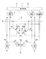
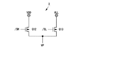
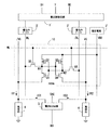
図1は、出力電圧が異なる第1および第2の高電位電源VDD,VLL(VDD>VLL)を使用した本発明の実施例1の半導体メモリの構成を示す図である。以下の説明において、特に断らない限り、High状態とはVDDもしくはVDD近傍の高レベルのことであり、Low状態とはGNDもしくはGND近傍の低レベルのことを示す。 FIG. 1 is a diagram showing a configuration of a semiconductor memory according to a first embodiment of the present invention using first and second high potential power supplies VDD and VLL (VDD> VLL) having different output voltages. In the following description, unless otherwise specified, the High state refers to VDD or a high level near VDD, and the Low state refers to GND or a low level near GND.
図1において、6トランジスタ構成(Q1〜Q6)のメモリセル10を使用すること、入力データDIの書込みを制御する書込制御回路1と一対のビット線BL,/BLをドライブする一対の書込みバッファ2で書込み回路を構成すること、擬似的な定電流源として機能する高抵抗4と電流センス回路5で読出し回路を構成することは、基本的に図10の従来例と同じである。但し、書込制御回路1と書込みバッファ2の機能は従来例よりも拡張されており、書込制御回路1の制御によって、書込みバッファ2の出力はVDDとGNDレベルの他に、第3の状態としてVLLレベル(VDDとGNDの中間レベル)をとれることが異なる。さらに、メモリセル10の高電位側電源端子を擬似電源線VPに接続すること、擬似電源線VPに接続された擬似電源線ドライバ3の出力電圧(VDDもしくはVLL)を書込制御回路1によって制御できることことが異なる。
In FIG. 1, a
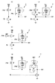
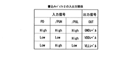
図2(a)は書込みバッファ2の回路図、図3(a)〜(f)は図2(a)中の低電圧プルアップ回路6の構成例である。図3(a)のpMOSFETQ10を使う構成、図3(d)のnMOSFETQ10’を使う構成の何れも適用可能である。また、図3(b),(c),(e),(f)のように、MOSFETQ10又はQ10’のオン電流を制限する手段として、MOSFETのソース又はドレインに直列に抵抗8を設けた構成も適用可能である。抵抗8は、抵抗素子の他、MOSFETのチャネル抵抗でも代用できる。図2(a)に示す書込みバッファ2の3個の制御入力(PD、/PUH、/PUL)は、High状態でVDDレベル、Low状態でGNDレベルをとる。これらの入力信号PD、/PUH、/PULと出力信号OUTの関係は、図14に示す通りである。
2A is a circuit diagram of the
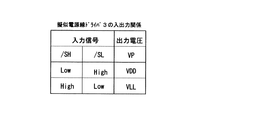
図5は擬似電源線ドライバ3の構成例である。2個の制御入力(/SH、/SL)は、High状態でVDDレベル、Low状態でGNDレベルをとる。これらの入力信号/SH、/SLと出力電圧VPの関係は、図15に示す通りである。
FIG. 5 is a configuration example of the pseudo power
上記の半導体メモリに対して、データを書き込む又は読み出す動作を以下に概説する。図1のメモリセル10にはデータ“1”が記憶されており、回路節点N1はHighレベル状態、回路節点N2はLowレベル状態にあるとする。
An operation of writing or reading data to or from the semiconductor memory will be outlined below. It is assumed that data “1” is stored in the
<スタンバイ状態>
図1の実施例1において、スタンバイ状態すなわちメモリセルアレイに対してデータの読出しも書込みも行わない状態における各部の電位関係について、以下に説明する。書込要求信号WEは非書込み状態(GNDレベル)、活性化信号SAEは非活性状態(GNDレベル)、凝似電源線VPはVLLレベルである。ワード線WLは非選択状態(GNDレベル)、ビット線BL,/BLはVLLレベル、擬似GND線VG,/VGはGNDレベルである。メモリセル10内のMOSFETに関しては、Q1,Q4は導通状態、Q2,Q3,Q5,Q6は非導通状態である。
<Standby state>
In the first embodiment of FIG. 1, the potential relationship of each part in the standby state, that is, the state where neither reading nor writing data to the memory cell array is described below. Write request signal WE is in a non-write state (GND level), activation signal SAE is in an inactive state (GND level), and similar power supply line VP is at a VLL level. The word line WL is in a non-selected state (GND level), the bit lines BL and / BL are at the VLL level, and the pseudo GND lines VG and / VG are at the GND level. Regarding the MOSFET in the
スタンバイ状態では、ビット線ペアBL,/BLと擬似電源線VPが共にVLLレベルに制御される。それ故、VDDが印加される従来例に比べると、MOSFETのサブスレッショルドリーク電流による無駄な消費電力は減少する。 In the standby state, both the bit line pair BL, / BL and the pseudo power supply line VP are controlled to the VLL level. Therefore, useless power consumption due to the subthreshold leakage current of the MOSFET is reduced as compared with the conventional example to which VDD is applied.
<読出し動作>
図1の実施例1において、メモリセル10に記憶されたデータ“1”を出力端子DOに読み出す動作は以下の通りである。読出し動作を通じて、書込要求信号WEは非書込み状態(GNDレベル)である。
<Read operation>
In the first embodiment of FIG. 1, the operation of reading the data “1” stored in the
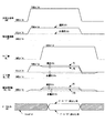
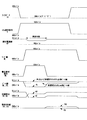
図6は図1の半導体メモリの主要な回路節点の動作波形である。一連の読出し動作の初期状態として、活性化信号SAEは非活性状態(GNDレベル)、凝似電源線VPはVLLレベルとする。ワード線WLは非選択状態(GNDレベル)、ビット線BL,/BLは共にVLLレベル、擬似GND線VG,/VGはGNDレベルである。メモリセル10内のMOSFETに関しては、Q1,Q4は導通状態、Q2,Q3,Q5,Q6は非導通状態である。
FIG. 6 shows operation waveforms at main circuit nodes of the semiconductor memory of FIG. As an initial state of a series of read operations, the activation signal SAE is in an inactive state (GND level), and the similar power supply line VP is at a VLL level. The word line WL is in a non-selected state (GND level), the bit lines BL and / BL are both at the VLL level, and the pseudo GND lines VG and / VG are at the GND level. Regarding the MOSFET in the
読出し動作は、当該コラムの活性化信号SAEをVDDレベルに制御して、電流センス回路5を活性状態にすると共に、擬似電源線ドライバ3を用いて当該コラムの擬似電源線VPの電位をVLLからVDDに昇圧することから始まる。その際、電流センス回路5から擬似GND線に定常的に流出する電流によって高抵抗4の両端に逆起電力が発生し、擬似GND線のレベルがGNDからGND近傍の低レベルまで上昇する。しかる後、ワード線WLを選択状態(VDDレベル)に制御する。以降の動作は、図12の従来例の説明と同じであり、重複を避ける為に説明を省略する。読出し対象のメモリセル10の擬似電源線VPには、従来例と同じくVDDなる電圧が印加されるので、本実施例によって動作速度は低下しない。
In the read operation, the activation signal SAE of the column is controlled to the VDD level to activate the
図1の半導体メモリでは省略されているが、ビット線ペアが複数ある場合は、出力端子DOの読出しデータDOを多重化して外部へ出力する為のマルチプレクサが電流センス回路5の後段に設けられる。その際、非選択コラムについては、電流センス回路が活性化されないので、ワード線が選択されてもデータは読み出されない。また、非選択コラムの擬似電源線VPは、VDDに昇圧されることはなく、VLLレベルを維持する。
Although omitted in the semiconductor memory of FIG. 1, when there are a plurality of bit line pairs, a multiplexer for multiplexing the read data DO of the output terminal DO and outputting it to the outside is provided at the subsequent stage of the
<書込み動作>
データ“1”が記憶された図1のメモリセル10に、入力端子DIから入力された逆データ“0”を書き込む動作について以下に述べる。書込み動作を通じて、活性化信号SAEは非活性状態(GNDレベル)、擬似電源線VPはVLLレベルである。
<Write operation>
An operation of writing the reverse data “0” input from the input terminal DI into the
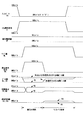
図7は図1の半導体メモリの主要な回路節点の動作波形である。一連の書込み動作の初期状態として、コラム選択信号Yは非選択状態(Lowレベル)、ワード線WLは非選択状態(GNDレベル)、書込要求信号WEは非書込み状態(GNDレベル)とする。ビット線BL側の書込みバッファ2の入力とビット線/BL側の書込みバッファ2の入力は共にLowレベルであり、ビット線BL,/BLは共にVLLレベルに設定されている。凝似GND線VG,/VGはGNDレベルである。メモリセル10内のMOSFETに関しては、Q1,Q4は導通状態、Q2,Q3,Q5,Q6は非導通状態である。
FIG. 7 shows operation waveforms at main circuit nodes of the semiconductor memory of FIG. As an initial state of a series of write operations, the column selection signal Y is in a non-selection state (Low level), the word line WL is in a non-selection state (GND level), and the write request signal WE is in a non-write state (GND level). Both the input of the
入力端子DIに入力されたデータ“0”の書込み動作は、コラム選択信号Yを選択状態(VDDレベル)にして、ビット線ペアを特定することから始まる。しかる後、ワード線WLを選択状態(VDDレベル)、書込要求信号WEを書込み状態(VDDレベル)に制御する。その際、書込制御回路1の動作により、ビット線BL側の書込みバッファ2の入力がHighレベル状態に制御されるので、ビット線BLはGNDレベルにドライブされる。ビット線/BL側の書込みバッファ2については、その入力はLowレベル状態から変化しないので、ビット線/BLはVLLレベルを維持する。ビット線BLの電位の低下と共に、MOSFETQ5のゲート・ソース(ビット線BL側のMOSFET節点)間にはMOSFETの閾値電圧を超える十分大きな電圧が印加されることになり、MOSFETQ5は導通状態になる。その結果、回路節点N1の電位は低下し、Q2,Q4で構成されるインバータの論理閾値を下回ると、フリップフロップ回路の状態は反転し、回路節点N1がLowレベル状態、回路節点N2がHighレベル状態に変化して、メモリセル10は更新データを保持可能になる。上記の動作は、電源電圧が異なるだけで、書込み動作そのものは図13の従来例と同じある。重複を避ける為に、以降の動作説明を省略する。
The write operation of the data “0” input to the input terminal DI starts by setting the column selection signal Y to the selected state (VDD level) and specifying the bit line pair. Thereafter, the word line WL is controlled to the selected state (VDD level), and the write request signal WE is controlled to the write state (VDD level). At this time, the operation of the
書込み期間に続くリカバリ期間(図7参照)において、擬似電源線VPとビット線(BL,/BL)をVLLもしくはVLL近傍のレベルに制御できるのは、例えばOE信号とWE信号間で論理をとることで、リカバリ動作と読出し動作を区別できることによる。ここで、OE信号とは、入出力ピンを共通化したデータI/Oバッファに関して、データ入力モードとデータ出力モードを切り替える信号である。書込み期間とリカバリ期間は共にでデータ入力モード、読出し期間はデータ出力モードに制御する。 In the recovery period (see FIG. 7) following the writing period, the pseudo power supply line VP and the bit lines (BL, / BL) can be controlled to VLL or a level near VLL, for example, by taking logic between the OE signal and the WE signal. This is because the recovery operation and the read operation can be distinguished. Here, the OE signal is a signal for switching a data input mode and a data output mode with respect to a data I / O buffer having a common input / output pin. The data input mode is controlled in both the writing period and the recovery period, and the data output mode is controlled in the reading period.
ビット線BL,/BLには大きな寄生容量があり、その充放電電流が書き込み時の消費電力の大半を占める。従って、実施例1のように、書込み時のビット線BL,/BLの振幅をVDD(従来例)からVLLに低減することで、書込み時の消費電力を(VLL/VDD)2に低減できる。 The bit lines BL and / BL have a large parasitic capacitance, and the charge / discharge current occupies most of the power consumption during writing. Therefore, the power consumption at the time of writing can be reduced to (VLL / VDD) 2 by reducing the amplitude of the bit lines BL and / BL at the time of writing from VDD (conventional example) to VLL as in the first embodiment.
なお、非選択コラムのビット線については、書込み動作を通じて、BL側も/BL側も書込みバッファ2によってVLL又はその近傍の中間レベルにプルアップされている。
Note that the bit lines of the non-selected columns are pulled up to VLL or an intermediate level in the vicinity thereof by the
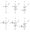
本発明の実施例1の変形例として、書込みバッファ2の別構成を図2(b)〜(d)に示す。これらの変形例は、選択状態のワード線WLの電位がVDDの場合、ビット線BL,/BLのレベルを「VDD−Vthn」以上に昇圧してもデータ読出し時の動作速度の改善に寄与しないという理論限界に着目して低電力化を図ったものである。書込みバッファ2の出力のHighレベルをVDDから「VDD−Vthn」に低減することで、データ読出し時のビット線の充放電による消費電力を
(VDD−Vthn)/VDD
に低減できる。ここで、VthnはnMOSFETの閾値電圧である。
As a modification of the first embodiment of the present invention, another configuration of the
Can be reduced. Here, Vthn is the threshold voltage of the nMOSFET.
書込みバッファ2の出力のHighレベルを「VDD−Vthn」に抑える手段として、図2(b)はダイオード接続されたnMOSFETQ9をMOSFETQ7に直列に接続している。また、図2(c)は、MOSFETQ7をpMOSからnMOSFETQ7’に置き換えている。構成は異なるが、図2(b)と(c)は同等の効果がある。さらに、図2(d)は、図2(b)のMOSFETQ9の挿入位置を変えた変形例であり、MOSFETQ7だけではなく低電圧プルアップ回路6に対しても直列になる位置にMOSFETQ9’を配置していることに特徴がある。データ読出し時に出力OUTのHighレベルを「VDD−Vthn」に抑えることは、図2(b)又は(c)の構成と同じである。差異はデータ書込み時の出力OUTのHighレベルにあり、図2(b)および(c)の構成がVLLであるのに対して、図2(d)の構成は「VLL−Vthn」となる。その結果、書込み時の消費電力を、図2(b)又は(c)の構成に比べて
(VLL−Vthn)/VLL
に低減できる。
As a means for suppressing the high level of the output of the
Can be reduced.
また、図2(d)の第2の特徴として、ダイオード接続されたMOSFETQ9’の両端に、書込制御回路1からのリセット信号/RSTで制御されるリセット回路7を具備することが挙げられる。VDD近傍に昇圧された擬似電源線VPのレベルをVLLもしくはVLL近傍に復帰させる際に、リセット信号/RSTをGNDレベルに制御してMOSFETQ9’のソースとドレインを短絡させる。
A second feature of FIG. 2D is that a
図4(a)と(b)はリセット回路7の具体例であり、pMOSFETQ11、nMOSFETQ11’の何れも適用可能である。その他、図4(c)、(d)のようにダイオード接続されたnMOSFETQ11”又はpMOSFETQ11’”も利用可能である。復帰される電圧は、ダイオード接続されたnMOS用いる場合は「VLL+Vthn」、ダイオード接続されたpMOSを用いる場合は「VLL+|Vthp|」になる。ここで、VthpはpMOSFETの閾値電圧(負値)である。
4 (a) and 4 (b) are specific examples of the
本発明の実施例2として、特に低消費電力化を追求する場合の構成について以下に述べる。サブスレッショルドリーク電流によるメモリセルアレイの消費電力を低減するには、VLLの値をできる限り低く設定することが有効である。VLLの理論上の下限は、
VLL>max(Vthn,|Vthp|)
で与えられる。このような低動作電圧条件では、書込みバッファ2の駆動力が低下する為に、ビット線BL,/BLをLowレベルに制御してもメモリセル10内のフリップフロップ回路を反転できないという現象が発生する。実施例2は、上記の問題に対処するものである。
As a second embodiment of the present invention, a configuration in particular when pursuing low power consumption will be described below. In order to reduce the power consumption of the memory cell array due to the subthreshold leakage current, it is effective to set the value of VLL as low as possible. The theoretical lower limit of VLL is
VLL> max (Vthn, | Vthp |)
Given in. Under such a low operating voltage condition, since the driving power of the
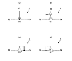
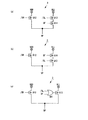
半導体メモリの構成は、図1に示す実施例1と同じである。実施例1とは、書込制御回路1および凝似電源線ドライバ3の機能が拡張されていることが異なり、データ書込み時の擬似電源線VPを開放状態(フローティング状態)に制御可能である。図8(a)〜(c)は、機能拡張された擬似電源線ドライバ3の回路図である。図8(a)はMOSFETQ13のドレイン側、図8(b)はMOSFETQ13のソース側にpMOSFETQ14を付加している。当該コラムの読出し時を除いて、/SH節点はVDDレベルに制御されているので、データを書き込む際は、SF入力をVDDレベルに制御することで出力VPをハイインピーダンス状態に設定できる。その結果、擬似電源線VPは開放状態になる。図8(c)は、論理ゲートOR1を使用した別構成であり、機能上は図8(a)又は(b)と同じである。
The configuration of the semiconductor memory is the same as that of the first embodiment shown in FIG. Unlike the first embodiment, the functions of the
図9は、機能拡張された擬似電源線ドライバ3を使用した際の半導体メモリの書込み動作波形である。データ書込み期間中、凝似電源線VPを開放状態に制御して電源からの電荷の供給を遮断することで、メモリセル10内のフリップフロップ回路の回路節点N1の電位をGNDレベルまで低下させられる。図7に示した実施例1の書込み動作波形との違いは、擬似電源線VPとメモリセル10内の回路節点N2の波形である。擬似電源線VPが開放状態の期間は、メモリセル10内のフリップフロップ回路のHigh側節点の電位は(VLL−Vth)であり、擬似電源線VPの開放状態が解除された時点で、VLLまで上昇する。このように機能拡張された擬似電源線ドライバ3を用いることで、書込みバッファ2の駆動力が低下する低電圧動作条件においても、データの確実な書込みを保証できる。
FIG. 9 shows a write operation waveform of the semiconductor memory when the function-expanded pseudo power
1,1’:書込み制御回路
2,2’:書込みバッファ
3:擬似電源線ドライバ
3’:固定電源
4:高抵抗
5:電流センス回路
6:低電圧プルアップ回路
7:リセット回路
8:電流制限抵抗
10:メモリセル
WL:ワード線
BL,/BL:ビット線ペア
VG,/VG:擬似GND線ペア
VP:擬似電源線
Q1,Q2,Q7,Q10,Q11,Q12,Q13,Q14,Q15:pMOSFET
Q3,Q4,Q5,Q6,Q7’,Q8,Q9,Q9’,Q10’,Q11’,Q11”,Q11”’,Q16:nMOSFET
INV1,INV2,INV3:インバータ
OR1:オアゲート
Y:コラム選択信号、入力端子、
SAE:活性化信号、入力端子
WE:書込要求信号、入力端子
DI:データの入力端子
DO:出力データ、出力端子
/PUH:ビット線のHighレベルプルアップ信号
/PUL:ビット線のLowレベルプルアップ信号
PD:ビット線のプルダウン信号
/RST:リセット信号
/SH:擬似電源線のHighレベル制御信号
/SL:擬似電源線のLowレベル制御信号
SF:擬似電源線の開放(フローティング)制御信号
N1,N2,G1,G2,T1,T2,T3,T4:回路節点
1, 1 ': Write
Q3, Q4, Q5, Q6, Q7 ', Q8, Q9, Q9', Q10 ', Q11', Q11 ", Q11"', Q16: nMOSFET
INV1, INV2, INV3: Inverter OR1: OR gate Y: Column selection signal, input terminal,
SAE: activation signal, input terminal WE: write request signal, input terminal DI: data input terminal DO: output data, output terminal / PUH: bit line high level pull-up signal / PUL: bit line low level pull Up signal PD: Bit line pull-down signal / RST: Reset signal / SH: Pseudo power supply line high level control signal / SL: Pseudo power supply line low level control signal SF: Pseudo power supply line open (floating) control signal N1, N2, G1, G2, T1, T2, T3, T4: circuit nodes
Claims (7)
出力電圧が異なる第1および第2の電源と、前記各書込みバッファのHigh出力レベルを前記第1又は第2の電源の電圧に対応する電圧に個々に切り替える手段と、前記擬似電源線のレベルを前記第1又は第2電源の電圧に対応する電圧に切り替える手段を設けたことを特徴とする半導体メモリ。 A flip-flop circuit comprising a pair of load MOSFETs and a pair of drive MOSFETs, a memory cell comprising a pair of cell selection MOSFETs connected to one and the other input / output sides of the flip-flop circuit, and the pair of cell selections A pair of bit lines connected to drains or sources opposite to the side connected to the flip-flop circuit of the power MOSFET, a pseudo power supply line commonly connected to the sources of the pair of load MOSFETs, and the pair of driving In a semiconductor memory having a pair of pseudo GND lines respectively connected to the sources of MOSFETs, a pair of write buffers connected to the pair of bit lines, and a current sense circuit commonly connected to the pair of pseudo GND lines,
First and second power supplies having different output voltages, means for individually switching the High output level of each write buffer to a voltage corresponding to the voltage of the first or second power supply, and the level of the pseudo power supply line A semiconductor memory comprising means for switching to a voltage corresponding to the voltage of the first or second power source.
前記擬似電源線を開放状態にする手段を設けたことを特徴とする半導体メモリ。 The semiconductor memory according to claim 1,
A semiconductor memory comprising means for opening the pseudo power supply line.
スタンバイ状態時に、前記擬似電源線と前記一対のビット線を、前記第1および第2の電源のうちの低い電圧の電源に対応する第1のHighレベルに制御する手段を設けたことを特徴とする半導体メモリ。 The semiconductor memory according to claim 1 or 2,
Means is provided for controlling the pseudo power supply line and the pair of bit lines to a first high level corresponding to a low-voltage power supply of the first and second power supplies in a standby state. Semiconductor memory.
メモリセルからのデータの読み出しの際に、当該メモリセルの擬似電源線と一対のビット線を、前記第1および第2の電源のうちの高い電圧の電源に対応する第2のHighレベルに制御し、非選択状態のメモリセルの擬似電源線と一対のビット線を、前記第1および第2の電源のうちの低い電圧の電源に対応する第1のHighレベルに制御する手段を設けたことを特徴とする半導体メモリ。 The semiconductor memory according to claim 1 or 2,
When reading data from the memory cell, the pseudo power supply line and the pair of bit lines of the memory cell are controlled to the second high level corresponding to the high voltage power supply of the first and second power supplies. And a means for controlling the pseudo power supply line and the pair of bit lines of the memory cell in the non-selected state to a first high level corresponding to a low voltage power supply of the first and second power supplies. A semiconductor memory characterized by the above.
メモリセルへのデータの書き込みの際に、当該メモリセルの擬似電源線と一対のビット線のうちのHigh側ビット線を、前記第1および第2の電源のうちの低い電圧の電源に対応する第1のHighレベルに制御する手段を設けたことを特徴とする半導体メモリ。 The semiconductor memory according to claim 1,
When writing data to the memory cell, the pseudo power line of the memory cell and the high-side bit line of the pair of bit lines correspond to the low voltage power source of the first and second power sources. A semiconductor memory comprising means for controlling to a first high level.
前記擬似電源線を開放状態にする手段を設け、
メモリセルへのデータの書込みの際に、当該メモリセルの擬似電源線を開放状態に制御し、かつ当該メモリセルの一対のビット線のうちのHigh側ビット線を、前記第1および第2の電源のうちの低い電圧の電源に対応する第1のHighレベルに制御する手段を設けたことを特徴とする半導体メモリ。 The semiconductor memory according to claim 1,
Means for opening the pseudo power supply line;
When writing data to the memory cell, the pseudo power supply line of the memory cell is controlled to be in an open state, and the high-side bit line of the pair of bit lines of the memory cell is set to the first and second A semiconductor memory comprising means for controlling to a first high level corresponding to a low-voltage power supply among power supplies.
前記第1のHighレベルに制御する手段に前記第1の電源を使用し、前記第2のHighレベルに制御する手段に前記第2の電源を使用することを特徴とする半導体メモリ。 The semiconductor memory according to any one of claims 3 to 6,
A semiconductor memory characterized in that the first power source is used for the means for controlling to the first High level, and the second power source is used for the means for controlling to the second High level.
Priority Applications (1)
| Application Number | Priority Date | Filing Date | Title |
|---|---|---|---|
| JP2004109059A JP2005293751A (en) | 2004-04-01 | 2004-04-01 | Semiconductor memory |
Applications Claiming Priority (1)
| Application Number | Priority Date | Filing Date | Title |
|---|---|---|---|
| JP2004109059A JP2005293751A (en) | 2004-04-01 | 2004-04-01 | Semiconductor memory |
Publications (1)
| Publication Number | Publication Date |
|---|---|
| JP2005293751A true JP2005293751A (en) | 2005-10-20 |
Family
ID=35326512
Family Applications (1)
| Application Number | Title | Priority Date | Filing Date |
|---|---|---|---|
| JP2004109059A Pending JP2005293751A (en) | 2004-04-01 | 2004-04-01 | Semiconductor memory |
Country Status (1)
| Country | Link |
|---|---|
| JP (1) | JP2005293751A (en) |
Cited By (2)
| Publication number | Priority date | Publication date | Assignee | Title |
|---|---|---|---|---|
| US7826298B2 (en) | 2007-05-24 | 2010-11-02 | Renesas Electronics Corporation | Semiconductor memory device with low standby current |
| JP2013254531A (en) * | 2012-06-05 | 2013-12-19 | Fujitsu Semiconductor Ltd | Semiconductor memory and system |
Citations (7)
| Publication number | Priority date | Publication date | Assignee | Title |
|---|---|---|---|---|
| JPS58122693A (en) * | 1982-01-14 | 1983-07-21 | Nippon Telegr & Teleph Corp <Ntt> | Memory circuit |
| JPH07141883A (en) * | 1993-11-18 | 1995-06-02 | Fujitsu Ltd | Static RAM |
| JPH1031888A (en) * | 1996-07-15 | 1998-02-03 | Ricoh Co Ltd | Semiconductor memory circuit |
| JPH11260055A (en) * | 1998-12-25 | 1999-09-24 | Hitachi Ltd | Semiconductor device |
| JP2000057778A (en) * | 1998-08-18 | 2000-02-25 | Nippon Telegr & Teleph Corp <Ntt> | Semiconductor memory |
| JP2003016786A (en) * | 2001-06-28 | 2003-01-17 | Mitsubishi Electric Corp | Semiconductor storage device |
| JP2003123479A (en) * | 2001-10-12 | 2003-04-25 | Matsushita Electric Ind Co Ltd | Semiconductor storage device |
-
2004
- 2004-04-01 JP JP2004109059A patent/JP2005293751A/en active Pending
Patent Citations (7)
| Publication number | Priority date | Publication date | Assignee | Title |
|---|---|---|---|---|
| JPS58122693A (en) * | 1982-01-14 | 1983-07-21 | Nippon Telegr & Teleph Corp <Ntt> | Memory circuit |
| JPH07141883A (en) * | 1993-11-18 | 1995-06-02 | Fujitsu Ltd | Static RAM |
| JPH1031888A (en) * | 1996-07-15 | 1998-02-03 | Ricoh Co Ltd | Semiconductor memory circuit |
| JP2000057778A (en) * | 1998-08-18 | 2000-02-25 | Nippon Telegr & Teleph Corp <Ntt> | Semiconductor memory |
| JPH11260055A (en) * | 1998-12-25 | 1999-09-24 | Hitachi Ltd | Semiconductor device |
| JP2003016786A (en) * | 2001-06-28 | 2003-01-17 | Mitsubishi Electric Corp | Semiconductor storage device |
| JP2003123479A (en) * | 2001-10-12 | 2003-04-25 | Matsushita Electric Ind Co Ltd | Semiconductor storage device |
Cited By (2)
| Publication number | Priority date | Publication date | Assignee | Title |
|---|---|---|---|---|
| US7826298B2 (en) | 2007-05-24 | 2010-11-02 | Renesas Electronics Corporation | Semiconductor memory device with low standby current |
| JP2013254531A (en) * | 2012-06-05 | 2013-12-19 | Fujitsu Semiconductor Ltd | Semiconductor memory and system |
Similar Documents
| Publication | Publication Date | Title |
|---|---|---|
| US10325650B2 (en) | Semiconductor storage device | |
| KR100718429B1 (en) | Semiconductor memory devices, semiconductor integrated circuit devices and portable devices | |
| JP6830681B2 (en) | Electronic circuit | |
| JP5122449B2 (en) | Integrated circuit having different power supply voltage for memory different from logic circuit power supply voltage | |
| US7986571B2 (en) | Low power, single-ended sensing in a multi-port SRAM using pre-discharged bit lines | |
| US8164971B2 (en) | Dual power rail word line driver and dual power rail word line driver array | |
| US6373745B2 (en) | Semiconductor memory cell and semiconductor memory device | |
| US5187686A (en) | Control circuit having outputs with differing rise and fall times | |
| US20040243758A1 (en) | Data storage circuit | |
| JP2003258624A (en) | Input buffer circuit and semiconductor memory | |
| JPH09231767A (en) | Static semiconductor memory device | |
| JP6578413B2 (en) | Semiconductor device | |
| JP4562515B2 (en) | Logic circuit and word driver circuit | |
| JP2005293751A (en) | Semiconductor memory | |
| Nautiyal et al. | Charge recycled low power SRAM with integrated write and read assist, for wearable electronics, designed in 7nm FinFET | |
| JP2014164777A (en) | SRAM | |
| JP4342467B2 (en) | Semiconductor memory | |
| JPH0330234B2 (en) | ||
| KR100278981B1 (en) | Variable voltage data recording device of semiconductor memory | |
| JPH1139865A (en) | Word line drive circuit | |
| JP2003257182A (en) | Static ram | |
| JPH0524594B2 (en) | ||
| JP2014123932A (en) | Semiconductor device | |
| JP2009043302A (en) | Data writing circuit and semiconductor memory device using the same |
Legal Events
| Date | Code | Title | Description |
|---|---|---|---|
| A621 | Written request for application examination |
Free format text: JAPANESE INTERMEDIATE CODE: A621 Effective date: 20060912 |
|
| A977 | Report on retrieval |
Free format text: JAPANESE INTERMEDIATE CODE: A971007 Effective date: 20090525 |
|
| A131 | Notification of reasons for refusal |
Free format text: JAPANESE INTERMEDIATE CODE: A131 Effective date: 20090603 |
|
| A521 | Written amendment |
Free format text: JAPANESE INTERMEDIATE CODE: A523 Effective date: 20090730 |
|
| A131 | Notification of reasons for refusal |
Free format text: JAPANESE INTERMEDIATE CODE: A131 Effective date: 20100316 |
|
| A02 | Decision of refusal |
Free format text: JAPANESE INTERMEDIATE CODE: A02 Effective date: 20100713 |