JP2005293489A - Random number generator - Google Patents
Random number generator Download PDFInfo
- Publication number
- JP2005293489A JP2005293489A JP2004111230A JP2004111230A JP2005293489A JP 2005293489 A JP2005293489 A JP 2005293489A JP 2004111230 A JP2004111230 A JP 2004111230A JP 2004111230 A JP2004111230 A JP 2004111230A JP 2005293489 A JP2005293489 A JP 2005293489A
- Authority
- JP
- Japan
- Prior art keywords
- random number
- number generation
- negative differential
- differential resistance
- generation circuit
- Prior art date
- Legal status (The legal status is an assumption and is not a legal conclusion. Google has not performed a legal analysis and makes no representation as to the accuracy of the status listed.)
- Granted
Links
Images

Abstract
【課題】高速で、回路規模が小さく、かつ消費電力の少ない乱数発生回路として複数の負性微分抵抗素子を用いる回路構成が知られている。従来この構成では、負性微分素子の極大電流値が等しいことが要求され、回路設計上の難点となっていた。本発明においては、極大電流値のばらつきの影響が少なく、かつ高速で、低消費電力の乱数発生回路の実現を目的とした。
【解決手段】直列に接続した2つの負性微分抵抗素子の接続点に電源電圧の1/2の電圧を印加することにより、これら負性微分抵抗素子回路の不安定点に一致させて初期状態とする。次に駆動用トランジスタをOFF状態としてこの電圧を取り除くと、出力点が上記不安定点から論理1または0のどちらかの安定点に遷移することを利用して乱数を発生させる構成とした。
【選択図】図1
A circuit configuration using a plurality of negative differential resistance elements is known as a random number generation circuit which is high speed, has a small circuit scale, and consumes less power. Conventionally, in this configuration, the negative differential elements are required to have the same maximum current value, which has been a difficulty in circuit design. An object of the present invention is to realize a random number generation circuit that is less affected by variations in the maximum current value, is high speed, and has low power consumption.
By applying a voltage half the power supply voltage to the connection point of two negative differential resistance elements connected in series, the initial state is matched with the unstable point of these negative differential resistance element circuits. To do. Next, when the driving transistor is turned off and this voltage is removed, the output point changes from the unstable point to the stable point of either logic 1 or 0 to generate a random number.
[Selection] Figure 1
Description
本発明は、自然乱数の高速発生が可能で、低消費電力であり、かつ占有面積を小さくし得る小回路規模な乱数発生回路に関する。 The present invention relates to a small-scale random number generation circuit capable of generating natural random numbers at high speed, having low power consumption, and capable of reducing an occupied area.
乱数を得る方法としては、予め定められたプログラムによって乱数を発生する擬似乱数発生法と、自然界で生じる確率的事象を利用した自然乱数発生法との2つが挙げられる。ともに、暗号化通信における鍵の生成などに利用されるが、前者はアルゴリズムが知られてしまうと、生成される乱数が予測できるが、後者は文宇通り、自然界で確率的に生じる事象を利用するため、予測不可能な真の乱数が得られる。このため、後者の自然界における確率事象を利用する方法による乱数発生を用いることが通信における情報の暗号化には最適とされている。 There are two methods for obtaining a random number: a pseudo-random number generation method that generates a random number using a predetermined program, and a natural random number generation method that uses a probabilistic event that occurs in nature. Both are used for key generation in encrypted communication, etc., but the former can predict the generated random numbers once the algorithm is known, but the latter uses events that occur probabilistically in the natural world as we Therefore, a true random number that cannot be predicted is obtained. For this reason, the use of random number generation by the latter method of utilizing a probability event in the natural world is considered optimal for information encryption in communication.
従来の自然乱数を得る方法として、抵抗体を用意し、熱雑音によって生じる抵抗値の揺らぎを電圧変換し、さらに増幅器によって雑音信号を増幅し、得られる雑音信号に対して、予め定めた閾値と比較することで、論理値“0”または“1”の判定を行い、乱数を得るという方法がある。 As a conventional method for obtaining a natural random number, a resistor is prepared, a resistance value fluctuation caused by thermal noise is converted into a voltage, a noise signal is amplified by an amplifier, and a predetermined threshold is set for the obtained noise signal. There is a method of determining a logical value “0” or “1” by comparison and obtaining a random number.
あるいは、下記(特許文献1)で開示されている負性微分抵抗素子を用いた、高速かつ低電力消費を満たしながら乱数を得る方法もある。これは二つの極大電流値の等しい負性微分抵抗素子を直列に接続した回路を振動型の電圧で駆動し、その際、雑音によって2つの素子の極大電流値の均衡を崩し、論理値“0”または“1”のどちらかに出力を決定する方法である。 Alternatively, there is a method of obtaining a random number while satisfying high speed and low power consumption using a negative differential resistance element disclosed in the following (Patent Document 1). In this method, a circuit in which two negative differential resistance elements having the same maximum current value are connected in series is driven by a vibration-type voltage. At this time, the balance between the maximum current values of the two elements is disturbed by noise, and a logical value “0” is obtained. This is a method of determining the output as either “1” or “1”.
上記の抵抗体の熱雑音によって生じる抵抗値の揺らぎは非常に微小であるため、信号増幅のため利得の大きな増幅器を用意する必要があり、結果として、乱数発生回路の大規模化およびそれに伴う消費電力の増大を引き起こす。据え置き型の端末であれば、このような乱数発生器を利用しても大きな問題は生じないが、携帯端末やスマートカード等、端末の物理的サイズが小さく、あらゆる回路部品の低消費電力化が望まれる場合にこれを利用することは不可能である。また、乱数の発生速度も240Mbit/s程度であり、最近の高速・大容量化するネットワークに対応するためには、より高速な乱数発生回路が要求される。 Since the resistance value fluctuation caused by the thermal noise of the resistor is very small, it is necessary to prepare an amplifier with a large gain for signal amplification. Causes an increase in power. If it is a stationary terminal, there will be no major problem even if such a random number generator is used, but the physical size of the terminal, such as a portable terminal or smart card, is small, and power consumption of all circuit components is reduced. It is impossible to use this if desired. Also, the random number generation speed is about 240 Mbit / s, and a higher-speed random number generation circuit is required to cope with the recent high-speed and large-capacity network.
このため、本発明においては、以上の問題点を解決した、高速、小回路規模(小占有面積)、かつ低消費電力の乱数発生回路を実現するため負性微分抵抗素子を利用する構成とした。しかし、従来技術では、熱雑音のような微小な揺らぎを検出するためには、回路中で使用する複数の負性微分抵抗素子の極大電流値をあらかじめ等しく揃えておく必要があった。 Therefore, in the present invention, a negative differential resistance element is used in order to realize a high-speed, small circuit scale (small occupied area) and low power consumption random number generation circuit that solves the above problems. . However, in the prior art, in order to detect minute fluctuations such as thermal noise, it is necessary to equalize the maximum current values of a plurality of negative differential resistance elements used in the circuit in advance.
しかし、実際上は、結晶構造の不均一性や素子作製工程上で生ずる素子面積の微小な揺らぎ(ばらつき)等により、上記の極大電流値を等しく揃えることは極めて困難であり、乱数を発生させるためには、極大電流値を等しく揃えるための回路上の工夫が不可欠となり、回路設計が困難になる、という問題があった。本発明では、上記課題を克服するために、素子特性のばらつきに対して影響が小さく、極大電流値に多少の大小があっても、極めて簡単な回路構成で高速かつ、低電力消費を満たしながら安定で実用性の高い自然乱数を得る回路を提供することを目的とした。 However, in practice, it is extremely difficult to equalize the above maximum current values due to non-uniformity in the crystal structure and minute fluctuations (variations) in the element area that occur in the element manufacturing process, and thus random numbers are generated. In order to achieve this, there is a problem in that it is indispensable to devise a circuit for equalizing the maximum current values, which makes circuit design difficult. In the present invention, in order to overcome the above-described problems, the influence on the variation in element characteristics is small, and even if the maximum current value is somewhat large and small, while satisfying high speed and low power consumption with a very simple circuit configuration. An object of the present invention is to provide a stable and practical circuit for obtaining natural random numbers.
上記目的を達成するために、本発明の請求項1においては、二つの負性微分抵抗素子を直列に接続して得られる回路の両端に直流電圧Vddを第一の電圧として印加し、前記回路の一方の端子には前記直流電圧Vddの高電位側を接続し、他方の端子には前記直流電圧Vddの低電位側、例えば接地電位を接続し、前記二つの負性微分抵抗素子の接続点に電界効果型トランジスタの第一の電極としてのソース電極を接続し、前記電界効果型トランジスタの第二の電極としてのドレイン電極に前記直流電圧Vddの2分の1の電圧すなわちVdd/2を第二の電圧として印加し、前記接続点を出力電圧Voutの出力点とし、前記電界効果型トランジスタの第三の電極としてのゲート電極に、振動電圧を印加することで、前記電界効果型トランジスタのON/OFFを制御し、前記電界効果型トランジスタがONの時に前記接続点に前記第2の電圧を印加し、前記電界効果型トランジスタがOFFの時に、前記接続点に印加されている第二の電圧を遮断し、この際、不可避的に加わる負性微分抵抗素子特性の熱揺らぎ、すなわち熱雑音、によって決定される出力を前記出力点から出力し、それを自然乱数として用いる構成について規定した。
In order to achieve the above object, in
請求項2においては、請求項1に記載の乱数発生回路において、電界効果型トランジスタの代わりにバイポーラトランジスタを用い、電界効果型トランジスタのゲート、ドレイン、ソースの各電極を、それぞれバイポーラトランジスタのべース、コレクタ、エミッタの各電極と置き換えた構成について規定した。 According to a second aspect of the present invention, in the random number generation circuit according to the first aspect, a bipolar transistor is used in place of the field effect transistor, and the gate, drain, and source electrodes of the field effect transistor are respectively connected to the base of the bipolar transistor. The configuration was replaced with each electrode of the collector, collector, and emitter.
請求項3においては、請求項1または請求項2に記載の乱数発生回路おいて、前記負性微分抵抗素子の少なくとも一方について、抵抗体を前記負性微分抵抗素子に並列に接続して得られる回路を複合負性微分抵抗素子として置き換えた構成について規定した。 According to a third aspect of the present invention, in the random number generation circuit according to the first or second aspect, at least one of the negative differential resistance elements is obtained by connecting a resistor in parallel to the negative differential resistance element. A configuration in which the circuit is replaced with a composite negative differential resistance element is defined.
請求項4においては、請求項1または請求項2に記載の乱数発生回路において、前記負性微分抵抗素子の少なくとも一方について、トランジスタを前記負性微分抵抗素子に並列に接続して得られる回路を複合負性微分抵抗素子として置き換えた構成について規定した。 According to a fourth aspect of the present invention, in the random number generation circuit according to the first or second aspect, a circuit obtained by connecting a transistor in parallel to the negative differential resistance element is provided for at least one of the negative differential resistance elements. The configuration replaced as a composite negative differential resistance element was defined.
請求項5においては、請求項1または請求項2に記載の乱数発生回路において、前記負性微分抵抗素子の少なくとも一方について、抵抗体とトランジスタとを前記負性微分抵抗素子に並列に接続して得られる回路を複合負性微分抵抗素子として置き換えた構成について規定した。 According to a fifth aspect of the present invention, in the random number generation circuit according to the first or second aspect, for at least one of the negative differential resistance elements, a resistor and a transistor are connected in parallel to the negative differential resistance element. A configuration in which the obtained circuit was replaced as a composite negative differential resistance element was defined.
請求項6においては、請求項1乃至請求項5の何れかに記載の乱数発生回路において、前記負性微分抵抗素子として共鳴トンネルダイオードを用いる構成について規定した。
In
請求項7においては、請求項1乃至請求項5の何れかに記載の乱数発生回路において、前記負性微分抵抗素子としてエサキダイオードを用いた構成について規定した。
In
請求項8においては、請求項1乃至請求項5の何れかに記載の乱数発生回路において、前記負性微分抵抗素子としてトランジスタで構成される負性微分抵抗特性を有する回路を用いた構成について規定した。 According to an eighth aspect of the present invention, in the random number generation circuit according to any one of the first to fifth aspects, a configuration using a circuit having a negative differential resistance characteristic formed of a transistor as the negative differential resistance element is defined. did.
請求項9においては、請求項1乃至請求項8の何れかに記載の乱数発生回路を複数個使用し、前記複数の乱数発生回路を並列に設置し、並列データ構成の乱数出力を得る構成について規定した。 In a ninth aspect of the present invention, a plurality of the random number generation circuits according to any one of the first to eighth aspects are used, and the plurality of random number generation circuits are installed in parallel to obtain a random number output having a parallel data configuration. Stipulated.
請求項10においては、請求項1乃至請求項8の何れかに記載の乱数発生回路を用い、単一の乱数発生回路を複数回サンプリングすることにより直列データ出力を得る構成について規定した。 The tenth aspect defines a configuration in which serial data output is obtained by sampling a single random number generation circuit a plurality of times using the random number generation circuit according to any one of the first to eighth aspects.
請求項11においては、請求項1乃至請求項10の何れかに記載の乱数発生回路において、前記電界効果型トランジスタまたは前記バイポーラトランジスタの前記第2の電極に前記第二の電圧Vdd/2を印加する方法として、前記二つの負性微分抵抗素子の直列接続回路への前記第一の電圧Vddと接地との間に同じ大きさの2本の抵抗体を直列に接続し、該2本の抵抗体の接続点から、前記第二の電圧Vdd/2を得、該第二の電圧Vdd/2を前記電界効果型トランジスタまたは前記バイポーラトランジスタの前記第二の電極に供給する構成について規定している。
11. The random number generation circuit according to
請求項12においては、請求項11に記載の乱数発生回路において、前記抵抗体の代わりに2個の直列接続したキャパシタを用い、該キャパシタの接続点から前記第二の電圧Vdd/2に相当する電圧を発生せしめる構成について規定している。 According to a twelfth aspect of the present invention, in the random number generation circuit according to the eleventh aspect, two series-connected capacitors are used instead of the resistor, and the second voltage Vdd / 2 corresponds to the connection point of the capacitors. It defines the configuration that generates voltage.
本発明によれば、2つの負性微分抵抗素子および1つの駆動用トランジスタの僅か3つの素子を用いるだけで高速で安定な乱数を発生させることができ、かつ2つの負性微分抵抗素子に要求される電気特性の均一性も緩和されるようになる。このため、本発明は高速、低消費電力を特長とする自然乱数発生回路の作製を容易にし、ならびに設計自由度の向上にも資するものである。 According to the present invention, it is possible to generate a high-speed and stable random number by using only three negative differential resistance elements and one driving transistor, and two negative differential resistance elements are required. The uniformity of the electrical characteristics is also eased. Therefore, the present invention facilitates the production of a natural random number generation circuit characterized by high speed and low power consumption, and contributes to improvement in design flexibility.
本発明は、負性微分抵抗素子を直列に接続した回路に直流電圧を印加し、2つの負性微分抵抗素子の接続点に接続されたトランジスタをON/OFFすることにより乱数発生回路動作の制御を行うことで、乱数発生動作を制御するものである。すなわち、駆動用トランジスタをON状態とすることで、負性微分抵抗素子を直列に接続した回路の出力電位を、2つの負性微分抵抗素子から得られる負荷曲線上の不安定点に一致させ、これを初期状態とし、そこから、駆動用トランジスタをOFF状態とすることで、負性微分抵抗素子に生じる雑音によって、出力電位が負荷曲線上の不安定点から、(0,1)どちらかの安定点に遷移することを利用して、乱数出力を得る。本回路では、2つの負性微分抵抗素子の極大電流値に多少の大小関係があっても、それが、負荷曲線上の不安定点における不安定性や、安定点へ遷移に大きな影響を与えることがないため、出来上がりの素子の電流−電圧特性に多少のばらつきがあっても、乱数を得る上で致命的な問題は生じない。わずかにでも雑音が生じさえすれば、安定点への遷移、すなわち(0,1)の出力分岐を得ること(熱雑音のような微小な揺らぎを検出すること)が充分可能となるのである。 The present invention controls the operation of a random number generation circuit by applying a DC voltage to a circuit in which negative differential resistance elements are connected in series, and turning on / off a transistor connected to the connection point of the two negative differential resistance elements. By controlling, random number generation operation is controlled. That is, by turning on the driving transistor, the output potential of the circuit in which the negative differential resistance elements are connected in series is matched with the unstable point on the load curve obtained from the two negative differential resistance elements. From the unstable point on the load curve due to the noise generated in the negative differential resistance element, by turning the drive transistor OFF from there, the stable point of either (0, 1) A random number output is obtained using the transition to. In this circuit, even if there is a slight magnitude relationship between the maximum current values of the two negative differential resistance elements, it may have a significant effect on the instability at the unstable point on the load curve and the transition to the stable point. Therefore, even if there are some variations in the current-voltage characteristics of the completed elements, no fatal problem arises in obtaining random numbers. If even a slight noise is generated, it is possible to obtain a transition to a stable point, that is, to obtain an output branch of (0, 1) (detection of minute fluctuations such as thermal noise).
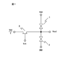
以下、本発明の実施の形態を図により説明する。図1はその回路図である。
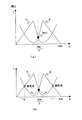
共鳴トンネルダイオード1および2を直列に接続し、この直列接続した回路の両端に直流電圧Vddを印加し、その一端にこの直流電圧の高電位側を接続し、他の一端にはを同じ直流電圧の低電位側、例えば接地電位(GND)を接続し、駆動用トランジスタ3のドレインにはVdd/2の直流電圧を印加し、ゲートには駆動用のクロック(Vck)を印加する。図2(a)および(b)は、この回路の動作原理を示すための直列接続した負性微分抵抗素子の電流(I)−電圧(V)特性である。図2(a)および(b)における負荷曲線4は共鳴トンネルダイオード1に、負荷曲線5は共鳴トンネルダイオード2に対応している。
Hereinafter, embodiments of the present invention will be described with reference to the drawings. FIG. 1 is a circuit diagram thereof.
クロックVckが高電位にある場合、トランジスタ3はON状態となり、図2(a)に示す様に、回路の出力電位Voutは、負荷曲線上の不安定点電圧Vdd/2に一致し、これに固定される。しかし、クロックVckが低電位(例えば接地電位)となると、トランジスタ3はOFF状態となり、2つの共鳴トンネルダイオード1および2の接続点に印加されていた電位Vdd/2が取り除かれるので出力点の電位Voutは不安定状態となる。
When the clock Vck is at a high potential, the
従ってこの場合は、図2(b)に示す様に、出力点の電位Voutは、必ず高電位側(“1”)か、低電位側(“0”)の何れか一方の安定点に遷移することになる。どちらの安定点に遷移するかは、少なくとも一方の共鳴トンネルダイオード1または2の電流(I)−電圧(V)特性に熱雑音由来の揺らぎが生じることによる負荷曲線の変化の様子によって決定される。
Therefore, in this case, as shown in FIG. 2B, the potential Vout at the output point always transits to either the high potential side (“1”) or the low potential side (“0”). Will do. The transition to which stable point is determined is determined by the state of change in the load curve due to fluctuations caused by thermal noise in the current (I) -voltage (V) characteristics of at least one
図3(a)のような負荷曲線(I−V特性)の熱雑音由来の揺らぎによる変化が生じた場合、すなわち例えば負荷曲線5が高電位側にシフトした場合(図3/a−1)、2つの共鳴トンネルダイオード1および2の接続点の電位、すなわち出力点の電位Vout、は低電位側の安定点に遷移し、出力点の論理レベル“0”が得られる。また、負荷曲線4が高電位側にシフトした場合(図3/a−2)においても出力点の電位は低電位側の安定点に遷移し、出力として論理レベル“0”が得られる。一方、図3(b)のような負荷曲線の変化が生じた場合、すなわち負荷曲線5が低電位側にシフトした場合(図3/b−1)、高電位側の安定点へ遷移し、出力点の論理レベル“1”が得られる。また、負荷曲線4が低電位側にシフトした場合(図3/b−2)、出力点の電位は高電位側の安定点に遷移し、出力点の電位“1”が得られる。図4は共鳴トンネルダイオードの電流−電圧特性に適当な揺らぎを与えた場合の出力変化の様子をシミュレーションで示したもので、下側の波形図は駆動用のトランジスタ3のゲートに印加したクロックVckの電圧波形で、上側の波形図は出力点Voutにおける電圧波形を示している。この場合の乱数発生速度(シミュレーションでは恣意的な揺らぎを与えているため、正確には乱数ではないことに注意)は1Gbit/sであり、出力振幅として0.7V程度が得られている。また、共鳴トンネルダイオードの電流−電圧特性における電流の絶対値が5%ほど揺らいだとしても、同様な出力波形を得ることができ、従来技術に比べ、2つの負性微分抵抗素子の電流−電圧特性に多少の違いがあっても、自然乱数が極めて簡単に得られることがわかる。
When the load curve (IV characteristic) changes due to fluctuations due to thermal noise as shown in FIG. 3A, that is, for example, when the
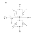
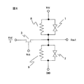
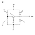
また、熱雑音による揺らぎの効果を大きくするために、図5に示すように、共鳴トンネルダイオード1および2にそれぞれ並列にダイオード接続したトランジスタ6および7を接続する回路構成、あるいは図6に示すように共鳴トンネルダイオード1および2にそれぞれ並列に抵抗体8および9を接続する構成も可能である。このような構成をとることによって、熱雑音による効果が拡大されるため周辺回路や環境に起因する外部雑音の影響を減らすことができ、回路作成上、外部雑音の遮蔽に関する要求条件が緩和される、という利点がある。しかしながら、共鳴トンネルダイオードのみで回路を構成した場合とくらべ、消費電力は大きくなってしまう。また、さらなる熱揺らぎの効果を得るために共鳴トンネルダイオードに並列にトランジスタと抵抗体の両者を接続する構成もあるが、この場合も、外部雑音の遮蔽に関する要求条件が緩和される。しかしながら、これら2方法においては、共鳴トンネルダイオードのみで回路を構成した場合と比べ、消費電力が大きくなることは避けられない。
Further, in order to increase the effect of fluctuation due to thermal noise, as shown in FIG. 5, a circuit configuration in which
さらにまた、これらの実施例における負性抵抗素子として、共鳴トンネルダイオードの代わりにエサキダイオードや、トランジスタを複数組み合わせて得られる負性微分抵抗特性を有する回路を用いても同様の発明の効果が得られる。しかしながら、エサキダイオードやトランジスタ回路に比べ、共鳴トンネルダイオードのスイッチング速度は速いため、高速乱数発生という観点では共鳴トンネルダイオードを用いた方がよい。さらに、共鳴トンネルダイオードの代わりにトランジスタで負性微分抵抗特性を有する回路を使用しても同様の結果を得ることが出来る。
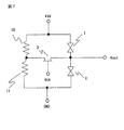
なお、駆動用トランジスタヘの印加電圧Vdd/2を確保するためには、図7に示すように、抵抗体10および11を直列接続し、その接続点から電圧Vdd/2を得る抵抗分割回路、あるいは図8に示すようにキャパシタ12および13を直列接続し、その接続点からVdd/2に相当する電圧を得る容量分割回路を用いてもよい。
Furthermore, the same effect of the invention can be obtained by using an Esaki diode instead of the resonant tunneling diode or a circuit having a negative differential resistance characteristic obtained by combining a plurality of transistors as the negative resistance element in these embodiments. It is done. However, since the switching speed of the resonant tunneling diode is faster than that of the Esaki diode or the transistor circuit, it is better to use the resonant tunneling diode from the viewpoint of high-speed random number generation. Further, similar results can be obtained even if a circuit having a negative differential resistance characteristic is used instead of the resonant tunneling diode.
In order to secure the applied voltage Vdd / 2 to the driving transistor, as shown in FIG. 7, a resistor dividing circuit that connects
以上の説明においては駆動用トランジスタとして電界効果型トランジスタを使用した場合について説明したが、電界効果型トランジスタのソース、ドレイン、ゲートの代わりにバイポーラトランジスタのエミッタ、コレクタ、ベースを使用しても同様の結果を得ることが出来る。
さらに、図1に示す回路を複数個並列に用意し、所望のbit数の並列データ出力としての乱数を得ることも可能である。また、例えば負性微分抵抗素子として共鳴トンネルダイオードを用いれば、回路の高速性を活かすことで、一つの回路で複数回のサンプリングを行い、所望のbit数の直列データ出力としての乱数を得ることも可能である。
In the above description, the case where a field effect transistor is used as the driving transistor has been described, but the same thing can be said even if the emitter, collector and base of a bipolar transistor are used instead of the source, drain and gate of the field effect transistor. The result can be obtained.
Further, it is possible to prepare a plurality of circuits shown in FIG. 1 in parallel and obtain a random number as a parallel data output of a desired number of bits. For example, if a resonant tunneling diode is used as a negative differential resistance element, sampling can be performed multiple times in one circuit by utilizing the high speed of the circuit, and a random number can be obtained as a serial data output of a desired number of bits. Is also possible.
1、2:共鳴トンネルダイオード
3:駆動用トランジスタ
4、5:負荷曲線(I−V特性)
6、7:トランジスタ
8、9、10、11:抵抗体
12、13:キャパシタ
1, 2: Resonant tunnel diode 3: Drive
6, 7:
Claims (12)
前記回路の一方の端子には前記直流電圧Vddの高電位側を接続し、
他方の端子には前記直流電圧Vddの低電位側を接続し、
前記二つの負性微分抵抗素子の接続点に電界効果型トランジスタの第一の電極としてのソース電極を接続し、
前記電界効果型トランジスタの第二の電極としてのドレイン電極に前記直流電圧Vddの2分の1の電圧すなわちVdd/2を第二の電圧として印加し、
前記接続点を出力電圧Voutの出力点とし、
前記電界効果型トランジスタの第三の電極としてのゲート電極に、振動電圧を印加することで、前記電界効果型トランジスタのON/OFFを制御し、
前記電界効果型トランジスタがONの時に前記接続点に前記第2の電圧を印加し、
前記電界効果型トランジスタがOFFの時に、前記接続点に印加されている第二の電圧を遮断し、この際、不可避的に加わる負性微分抵抗素子特性の熱揺らぎによって決定される出力を前記出力点から出力し、それを自然乱数として用いることを特徴とする乱数発生回路。 A DC voltage Vdd is applied as a first voltage across a circuit obtained by connecting two negative differential resistance elements in series,
One terminal of the circuit is connected to the high potential side of the DC voltage Vdd,
The other terminal is connected to the low potential side of the DC voltage Vdd,
A source electrode as a first electrode of a field effect transistor is connected to a connection point between the two negative differential resistance elements,
Applying a half voltage of the DC voltage Vdd, that is, Vdd / 2 as the second voltage to the drain electrode as the second electrode of the field effect transistor,
The connection point is an output point of the output voltage Vout,
By applying an oscillating voltage to the gate electrode as the third electrode of the field effect transistor, the ON / OFF of the field effect transistor is controlled,
Applying the second voltage to the connection point when the field effect transistor is ON;
When the field effect transistor is OFF, the second voltage applied to the connection point is cut off. At this time, the output determined by the thermal fluctuation of the negative differential resistance element characteristic unavoidably applied is output as the output. A random number generating circuit that outputs from a point and uses it as a natural random number.
電界効果型トランジスタの代わりにバイポーラトランジスタを用い、電界効果型トランジスタのゲート、ドレイン、ソースの各電極を、それぞれバイポーラトランジスタのべース、コレクタ、エミッタの各電極と置き換えることを特徴とする乱数発生回路。 The random number generation circuit according to claim 1,
Random number generation characterized by using bipolar transistors instead of field-effect transistors and replacing the gate, drain, and source electrodes of the field-effect transistor with the base, collector, and emitter electrodes of the bipolar transistor, respectively. circuit.
前記負性微分抵抗素子の少なくとも一方について、抵抗体を前記負性微分抵抗素子に並列に接続して得られる回路を複合負性微分抵抗素子として置き換えたことを特徴とする乱数発生回路。 In the random number generation circuit according to claim 1 or 2,
A random number generation circuit, wherein a circuit obtained by connecting a resistor in parallel to the negative differential resistance element is replaced with a composite negative differential resistance element for at least one of the negative differential resistance elements.
前記負性微分抵抗素子の少なくとも一方について、トランジスタを前記負性微分抵抗素子に並列に接続して得られる回路を複合負性微分抵抗素子として置き換えたことを特徴とする乱数発生回路。 In the random number generation circuit according to claim 1 or 2,
A random number generation circuit, wherein a circuit obtained by connecting a transistor in parallel with the negative differential resistance element is replaced with a composite negative differential resistance element for at least one of the negative differential resistance elements.
前記負性微分抵抗素子の少なくとも一方について、抵抗体とトランジスタとを前記負性微分抵抗素子に並列に接続して得られる複合負性微分抵抗素子に置き換えたことを特徴とする乱数発生回路。 In the random number generation circuit according to claim 1 or 2,
A random number generation circuit, wherein at least one of the negative differential resistance elements is replaced with a composite negative differential resistance element obtained by connecting a resistor and a transistor in parallel with the negative differential resistance element.
前記負性微分抵抗素子として共鳴トンネルダイオードを用いることを特徴とする乱数発生回路。 The random number generation circuit according to any one of claims 1 to 5,
A random number generation circuit using a resonant tunneling diode as the negative differential resistance element.
前記負性微分抵抗素子としてエサキダイオードを用いることを特徴とする乱数発生回路。 The random number generation circuit according to any one of claims 1 to 5,
A random number generation circuit using an Esaki diode as the negative differential resistance element.
前記負性微分抵抗素子としてトランジスタで構成される負性微分抵抗特性を有する回路を用いることを特徴とする乱数発生回路。 The random number generation circuit according to any one of claims 1 to 5,
A random number generation circuit using a circuit having a negative differential resistance characteristic composed of a transistor as the negative differential resistance element.
前記複数の乱数発生回路を並列に設置し、
並列データ構成の乱数出力を得ることを特徴とする乱数発生回路。 A plurality of random number generation circuits according to any one of claims 1 to 8 are used,
Installing the plurality of random number generation circuits in parallel;
A random number generation circuit characterized by obtaining a random number output of a parallel data configuration.
単一の乱数発生回路を複数回サンプリングすることにより直列データ出力を得ることを特徴とする乱数発生回路。 Using the random number generation circuit according to any one of claims 1 to 8,
A random number generation circuit characterized by obtaining a serial data output by sampling a single random number generation circuit a plurality of times.
前記電界効果型トランジスタまたは前記バイポーラトランジスタの前記第2の電極に前記第二の電圧Vdd/2を印加する方法として、
前記二つの負性微分抵抗素子の直列接続回路への前記第一の電圧Vddと接地との間に同じ大きさの2本の抵抗体を直列に接続し、該2本の抵抗体の接続点から、前記第二の電圧Vdd/2を得、該第二の電圧Vdd/2を前記電界効果型トランジスタまたは前記バイポーラトランジスタの前記第二の電極に供給することを特徴とする乱数発生回路。 The random number generation circuit according to any one of claims 1 to 8,
As a method of applying the second voltage Vdd / 2 to the second electrode of the field effect transistor or the bipolar transistor,
Two resistors of the same size are connected in series between the first voltage Vdd to the series connection circuit of the two negative differential resistance elements and the ground, and a connection point of the two resistors To obtain the second voltage Vdd / 2, and supply the second voltage Vdd / 2 to the second electrode of the field effect transistor or the bipolar transistor.
前記抵抗体の代わりに2個の直列接続したキャパシタを用い、該キャパシタの接続点から前記第二の電圧Vdd/2に相当する電圧を発生せしめることを特徴とする乱数発生回路。
The random number generation circuit according to claim 11,
A random number generation circuit using two capacitors connected in series instead of the resistor and generating a voltage corresponding to the second voltage Vdd / 2 from a connection point of the capacitors.
Priority Applications (1)
| Application Number | Priority Date | Filing Date | Title |
|---|---|---|---|
| JP2004111230A JP4252924B2 (en) | 2004-04-05 | 2004-04-05 | Random number generator |
Applications Claiming Priority (1)
| Application Number | Priority Date | Filing Date | Title |
|---|---|---|---|
| JP2004111230A JP4252924B2 (en) | 2004-04-05 | 2004-04-05 | Random number generator |
Publications (2)
| Publication Number | Publication Date |
|---|---|
| JP2005293489A true JP2005293489A (en) | 2005-10-20 |
| JP4252924B2 JP4252924B2 (en) | 2009-04-08 |
Family
ID=35326314
Family Applications (1)
| Application Number | Title | Priority Date | Filing Date |
|---|---|---|---|
| JP2004111230A Expired - Fee Related JP4252924B2 (en) | 2004-04-05 | 2004-04-05 | Random number generator |
Country Status (1)
| Country | Link |
|---|---|
| JP (1) | JP4252924B2 (en) |
Cited By (3)
| Publication number | Priority date | Publication date | Assignee | Title |
|---|---|---|---|---|
| GB2543125A (en) * | 2016-07-27 | 2017-04-12 | Quantum Base Ltd | Generating a unique response to a challenge |
| GB2543126A (en) * | 2016-07-27 | 2017-04-12 | Quantum Base Ltd | Generating a nondeterministic response to a challenge |
| GB2548428A (en) * | 2016-08-08 | 2017-09-20 | Quantum Base Ltd | Nondeterministic response to a challenge |
-
2004
- 2004-04-05 JP JP2004111230A patent/JP4252924B2/en not_active Expired - Fee Related
Cited By (10)
| Publication number | Priority date | Publication date | Assignee | Title |
|---|---|---|---|---|
| GB2543125A (en) * | 2016-07-27 | 2017-04-12 | Quantum Base Ltd | Generating a unique response to a challenge |
| GB2543126A (en) * | 2016-07-27 | 2017-04-12 | Quantum Base Ltd | Generating a nondeterministic response to a challenge |
| GB2543125B (en) * | 2016-07-27 | 2017-10-18 | Quantum Base Ltd | Generating a unique response to a challenge |
| GB2543126B (en) * | 2016-07-27 | 2017-10-25 | Quantum Base Ltd | Generating a nondeterministic response to a challenge |
| US11295003B2 (en) * | 2016-07-27 | 2022-04-05 | Quantum Base Limited | Generating a unique response to a challenge |
| GB2548428A (en) * | 2016-08-08 | 2017-09-20 | Quantum Base Ltd | Nondeterministic response to a challenge |
| WO2018029440A1 (en) * | 2016-08-08 | 2018-02-15 | Quantum Base Limited | Nondeterministic response to a challenge |
| GB2548428B (en) * | 2016-08-08 | 2018-05-16 | Quantum Base Ltd | Nondeterministic response to a challenge |
| US11061647B2 (en) | 2016-08-08 | 2021-07-13 | Quantum Base Limited | Nondeterministic response to a challenge |
| AU2017310491B2 (en) * | 2016-08-08 | 2021-09-09 | Quantum Base Limited | Nondeterministic response to a challenge |
Also Published As
| Publication number | Publication date |
|---|---|
| JP4252924B2 (en) | 2009-04-08 |
Similar Documents
| Publication | Publication Date | Title |
|---|---|---|
| JP5171908B2 (en) | Power circuit | |
| JP4921106B2 (en) | Buffer circuit | |
| US20030132872A1 (en) | Tail current node equalization for a variable offset amplifier | |
| JP2012048452A (en) | Semiconductor chip | |
| JP2009198476A (en) | Voltage detecting circuit | |
| US20170323669A1 (en) | Device and method for data-writing | |
| JP2010232959A (en) | Electronic circuit | |
| CN101465157A (en) | Circuit for generating dynamic self-adapting referrence of 1T1C ferro-electric memory | |
| JP4252924B2 (en) | Random number generator | |
| EP2599218A1 (en) | Low phase noise buffer for crystal oscillator | |
| US20110210794A1 (en) | Voltage sensing circuit capable of controlling a pump voltage stably generated in a low voltage environment | |
| JP4118754B2 (en) | Random number generator | |
| Uddin et al. | A practical sense amplifier design for memristive crossbar circuits (PUF) | |
| KR20050041592A (en) | Internal voltage generation device capable of temperature compensation | |
| JP2009015972A (en) | Semiconductor memory device | |
| KR20220170243A (en) | Ternary logic circuit | |
| CN115440277A (en) | Memristor-based XOR logic circuit | |
| JP2006189946A (en) | Random number generation circuit and semiconductor integrated circuit | |
| WO2008039624A2 (en) | Sense amplifier circuit for low voltage applications | |
| JP2006067497A (en) | Signal control circuit and device equipped with the same | |
| US20080238517A1 (en) | Oscillator Circuit and Semiconductor Device | |
| JP2013222474A (en) | Nonvolatile memory circuit, semiconductor device, and read method | |
| CN102201806A (en) | Circuit with current control mechanism and current control method | |
| JP2014154189A (en) | Resistance change type memory counter basis read-out circuit | |
| JP2008004153A (en) | Semiconductor memory device |
Legal Events
| Date | Code | Title | Description |
|---|---|---|---|
| A621 | Written request for application examination |
Free format text: JAPANESE INTERMEDIATE CODE: A621 Effective date: 20060714 |
|
| A977 | Report on retrieval |
Free format text: JAPANESE INTERMEDIATE CODE: A971007 Effective date: 20090115 |
|
| TRDD | Decision of grant or rejection written | ||
| A01 | Written decision to grant a patent or to grant a registration (utility model) |
Free format text: JAPANESE INTERMEDIATE CODE: A01 Effective date: 20090120 |
|
| A01 | Written decision to grant a patent or to grant a registration (utility model) |
Free format text: JAPANESE INTERMEDIATE CODE: A01 |
|
| A61 | First payment of annual fees (during grant procedure) |
Free format text: JAPANESE INTERMEDIATE CODE: A61 Effective date: 20090122 |
|
| R150 | Certificate of patent or registration of utility model |
Free format text: JAPANESE INTERMEDIATE CODE: R150 |
|
| FPAY | Renewal fee payment (event date is renewal date of database) |
Free format text: PAYMENT UNTIL: 20120130 Year of fee payment: 3 |
|
| FPAY | Renewal fee payment (event date is renewal date of database) |
Free format text: PAYMENT UNTIL: 20130130 Year of fee payment: 4 |
|
| LAPS | Cancellation because of no payment of annual fees |