JP2005293477A - Memory controller - Google Patents
Memory controller Download PDFInfo
- Publication number
- JP2005293477A JP2005293477A JP2004111091A JP2004111091A JP2005293477A JP 2005293477 A JP2005293477 A JP 2005293477A JP 2004111091 A JP2004111091 A JP 2004111091A JP 2004111091 A JP2004111091 A JP 2004111091A JP 2005293477 A JP2005293477 A JP 2005293477A
- Authority
- JP
- Japan
- Prior art keywords
- data
- state machine
- selector
- signal
- address
- Prior art date
- Legal status (The legal status is an assumption and is not a legal conclusion. Google has not performed a legal analysis and makes no representation as to the accuracy of the status listed.)
- Pending
Links
Images

Classifications
-
- G—PHYSICS
- G06—COMPUTING OR CALCULATING; COUNTING
- G06F—ELECTRIC DIGITAL DATA PROCESSING
- G06F13/00—Interconnection of, or transfer of information or other signals between, memories, input/output devices or central processing units
- G06F13/14—Handling requests for interconnection or transfer
- G06F13/16—Handling requests for interconnection or transfer for access to memory bus
- G06F13/1668—Details of memory controller
- G06F13/1689—Synchronisation and timing concerns
Landscapes
- Engineering & Computer Science (AREA)
- Theoretical Computer Science (AREA)
- Physics & Mathematics (AREA)
- General Engineering & Computer Science (AREA)
- General Physics & Mathematics (AREA)
- Microcomputers (AREA)
- Memory System (AREA)
Abstract
Description
本発明は、中央処理装置(CPU:Central Processing Unit)とSRAM(Static Random Access Memory)やROM(Read Only Memory)等の記憶装置の間で、読み書き動作のタイミング制御を行う汎用のメモリコントローラ、特にそのアクセスパラメータの設定に関するものである。 The present invention relates to a general-purpose memory controller that controls the timing of read / write operations between a central processing unit (CPU) and a storage device such as an SRAM (Static Random Access Memory) and a ROM (Read Only Memory), It relates to the setting of the access parameter.
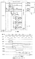
図2(a),(b)は、従来のメモリコントローラの説明図である。
図2(a)に示すように、メモリコントローラ10は、動作タイミングが異なるCPU1とSRAM2等のメモリの間で読み書き動作のタイミング制御を行うもので、主要構成要素であるステートマシン11に加えて、デコーダ12、レジスタ13、及びセレクタ14〜16を備えている。
2A and 2B are explanatory diagrams of a conventional memory controller.
As shown in FIG. 2A, the
ステートマシン11は、現在保持している状態(ステート)と与えられる信号(イベント)に対応して、予め定められている次の状態へ遷移する論理回路である。ステートマシン11には、CPU1側から、読み書き制御信号RWとアドレス信号ADの内の下位アドレスADLに加えて、上位アドレスADUをデコーダ12で解読して得られたチップ選択信号CS1が与えられるようになっている。ステートマシン11からSRAM2には、このSRAM2の特性に応じてタイミングが制御された読み書き制御信号MRW、チップ選択信号MCS、及びアドレス信号MADを出力するようになっている。また、CPU1に入出力されるデータ信号DTは、このステートマシン11によってタイミングが制御され、データ信号MDTとしてSRAM2に入出力されるようになっている。このステートマシン11は、CPU1と共通のクロック信号CKによって、動作タイミングが制御されるようになっている。
The state machine 11 is a logic circuit that makes a transition to a predetermined next state in accordance with a currently held state (state) and a given signal (event). In addition to the lower address ADL of the read / write control signal RW and the address signal AD, the state machine 11 is given a chip selection signal CS1 obtained by decoding the upper address ADU with the
デコーダ12は、上位アドレスADUを解読してSRAM2に対応するチップ選択信号CS1を出力するほか、このメモリコントローラ10中のレジスタ13に対応するチップ選択信号CS2を出力するようになっている。レジスタ13は、チップ選択信号CS2で選択されて読み書き制御信号RWで書き込みが指定されたときに、クロック信号CKのタイミングに従って、CPU1から出力されるデータ信号DTを記憶するものである。レジスタ13の記憶内容は、選択信号SLとしてセレクタ14〜16へ与えられるようになっている。
The
セレクタ14〜16は、それぞれ4つの入力データの内から、選択信号SLで指定されたデータを選択してステートマシン11に与えるものである。例えば、セレクタ14は、選択信号SLが“0”と“1”のときにはデータ“1”をアドレスセットアップ値ASUとしてステートマシン11に与え、選択信号SLが“2”と“3”のときにはデータ“2”をアドレスセットアップ値ASUとして与える。セレクタ15は、選択信号SLの“0”,“1”,“2”,“3”に対応して、それぞれデータ“1”,“2”,“3”,“5”を、アサートパルス幅APWとしてステートマシン11に与える。更に、セレクタ16は、選択信号SLの“0”,“1”,“2”,“3”に対応して、それぞれデータ“1”,“2”,“3”,“3”を、データオフ値DOFとしてステートマシン11に与えるようになっている。
Each of the
次に動作を説明する。
電源投入時の初期設定により、CPU1によってSRAM2の種別等が読み出され、このSRAM2に応じたアドレスセットアップ値ASU、アサートパルス幅APW、及びデータオフ値DOFの組み合わせを選択するための選択情報が、このCPU1からレジスタ13に書き込まれる。ここでは、レジスタ13に“1”が書き込まれたとする。これにより、セレクタ14で入力データ“1”が選択され、アドレスセットアップ値ASUとしてステートマシン11に与えられる。セレクタ15では、入力データ“2”が選択され、アサートパルス幅APWとしてステートマシン11に与えられる。更に、セレクタ16では、入力データ“2”が選択され、データオフ値DOFとしてステートマシン11に与えられる。
Next, the operation will be described.
By the initial setting at power-on, the
次に、CPU1からSRAM2に対するアクセスが開始され、これらのアドレスセットアップ値ASU、アサートパルス幅APW、及びデータオフ値DOFに基づいてタイミング制御が行われ、SRAM2に対する読み書きのアクセスが実行される。
Next, access from the
図2(b)の時刻T1におけるクロック信号CKの立ち上がりで、このSRAM2を指定するアドレス信号ADと、読み書き制御信号RWが出力される。アドレス信号ADの上位アドレスADUはデコーダ12で解読され、チップ選択信号CS1がステートマシン11に与えられる。下位アドレスADLと読み書き制御信号RWは、そのままステートマシン11に与えられる。
At the rise of the clock signal CK at time T1 in FIG. 2B, the address signal AD designating the
時刻T2における次のクロック信号CKの立ち上がりで、ステートマシン11からSRAM2に対するチップ選択信号MCSが出力される。また、CPU1からデータ信号DTの出力が開始され、このCPU1から出力されていたアドレス信号ADと読み書き制御信号RWは、この時点で停止される。
At the rise of the next clock signal CK at time T2, the chip selection signal MCS for the
時刻T2から、アドレスセットアップ値ASUで指定された1クロック期間が経過すると、時刻T3におけるクロック信号CKの立ち上がりで、ステートマシン11からSRAM2に対するアドレス信号MADが出力される。
When one clock period designated by the address setup value ASU elapses from time T2, the address signal MAD for the
時刻T4における次のクロック信号CKの立ち上がりで、ステートマシン11からSRAM2に対するデータ信号MDTが出力され、CPU1とSRAM2間のデータ転送が開始される。
At the rise of the next clock signal CK at time T4, the data signal MDT for the
時刻T3から、アサートパルス幅APWで指定された2クロック期間が経過すると、時刻T5におけるクロック信号CKの立ち上がりで、ステートマシン11から出力されていたチップ選択信号MCSと読み書き制御信号MRWが停止する。 When two clock periods specified by the assert pulse width APW elapse from time T3, the chip selection signal MCS and the read / write control signal MRW output from the state machine 11 are stopped at the rising edge of the clock signal CK at time T5.
更に、時刻T5から、データオフ値DOFで指定された2クロック期間が経過すると、時刻T6におけるクロック信号CKの立ち上がりで、ステートマシン11から出力されていたデータ信号MDTが停止する。これにより、SRAM2のアドレスMADへのアクセスは完了する。 Furthermore, when two clock periods specified by the data off value DOF have elapsed from time T5, the data signal MDT output from the state machine 11 stops at the rising edge of the clock signal CK at time T6. Thereby, the access to the address MAD of the SRAM 2 is completed.
しかしながら、前記メモリコントローラ10は、設定可能なアドレスセットアップ値ASU、アサートパルス幅APW、及びデータオフ値DOFの組み合わせが限定されていた。即ち、選択信号SL=0のとき(ASU=1,APW=1,DOF=1)、選択信号SL=1のとき(ASU=1,APW=2,DOF=2)、選択信号SL=2のとき(ASU=2,APW=3,DOF=3)、選択信号SL=3のとき(ASU=2,APW=5,DOF=3)の4種類しか選択することができず、かつ、パラメータの組み合わせが固定化されている。また、選択範囲を広げるためには、セレクタ14〜16の入力データ数を大幅に増加させる必要があり、回路規模が大きくなるという課題があった。
However, the
本発明は、回路規模の増加を抑制しつつ、自由なパラメータ設定が可能なメモリコントローラを提供することを目的としている。 An object of the present invention is to provide a memory controller capable of freely setting parameters while suppressing an increase in circuit scale.
本発明のメモリコントローラは、CPUと記憶装置の間で転送される制御信号、アドレス信号及びデータ信号のタイミングを与えられたパラメータに従って制御するステートマシンと、前記CPUから与えられた選択情報と加算情報を保持するレジスタと、前記選択情報に従って複数のデータの中から該当するデータを選択するセレクタと、前記セレクタで選択されたデータに前記加算情報を加算してその加算結果を前記パラメータとして前記ステートマシンに与える加算器とを備えたことを特徴としている。 The memory controller of the present invention includes a state machine that controls the timing of a control signal, an address signal, and a data signal transferred between a CPU and a storage device in accordance with given parameters, and selection information and addition information given from the CPU. A selector for selecting corresponding data from a plurality of data according to the selection information, and adding the addition information to the data selected by the selector and using the addition result as the parameter for the state machine And an adder to be provided.
本発明では、セレクタによって選択情報に従って複数のデータの中から該当するデータを選択し、このセレクタで選択されたデータに加算情報を加算してその加算結果をパラメータとしてステートマシンに与えるようにしている。これにより、回路規模を大幅に増加させることなく、ステートマシンに与えるパラメータの設定範囲を拡大することができるという効果がある。 In the present invention, the selector selects corresponding data from a plurality of data according to the selection information, adds the addition information to the data selected by the selector, and gives the addition result to the state machine as a parameter. . As a result, there is an effect that the parameter setting range given to the state machine can be expanded without greatly increasing the circuit scale.
CPUと記憶装置の間で転送される制御信号、アドレス信号及びデータ信号のタイミングを、アドレスセットアップ値、アサートパルス幅、及びデータオフ値の3つのパラメータに従って制御するステートマシンに対して、各パラメータに対応して設けられた3つのセレクタで、第1の選択情報に基づいてそれぞれ複数のデータの中から該当するデータを選択する。そして、3つのセレクタの内で第2の選択情報に該当するセレクタで選択されたデータには、加算情報を加算してパラメータとしてステートマシンへ与え、この第2の選択情報に該当しないセレクタで選択されたデータはそのままパラメータとしてステートマシンへ与える。 For each state machine that controls the timing of the control signal, address signal, and data signal transferred between the CPU and the storage device according to the three parameters of the address setup value, assert pulse width, and data off value, Corresponding data is selected from a plurality of data based on the first selection information by three selectors provided correspondingly. Of the three selectors, the data selected by the selector corresponding to the second selection information is added with the addition information and given to the state machine as a parameter, and selected by the selector not corresponding to the second selection information. The processed data is directly given to the state machine as a parameter.
この発明の前記並びにその他の目的と新規な特徴は、次の好ましい実施例の説明を添付図面と照らし合わせて読むと、より完全に明らかになるであろう。但し、図面は、もっぱら解説のためのものであって、この発明の範囲を限定するものではない。 The above and other objects and novel features of the present invention will become more fully apparent when the following description of the preferred embodiment is read in conjunction with the accompanying drawings. However, the drawings are for explanation only, and do not limit the scope of the present invention.
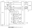
図1は、本発明の実施例1を示すメモリコントローラの構成図であり、図2中の要素と共通の要素には共通の符号が付されている。 FIG. 1 is a configuration diagram of a memory controller showing a first embodiment of the present invention. Elements common to those in FIG. 2 are denoted by common reference numerals.
このメモリコントローラ10Aは、動作タイミングが異なるCPU1とSRAM2やROM等の記憶装置の間で読み書き動作のタイミング制御を行うもので、主要構成要素であるステートマシン11に加えて、デコーダ12、レジスタ13A、セレクタ14〜16、及び加算器17〜19を備えている。
This
ステートマシン11は、現在保持している状態と与えられる信号に対応して、与えられたパラメータに従って、予め定められている次の状態へ遷移する論理回路である。ステートマシン11には、CPU1側から、読み書き制御信号RW等の制御信号及びアドレス信号ADの内の下位アドレスADLに加えて、上位アドレスADUをデコーダ12で解読して得られたチップ選択信号CS1が与えられるようになっている。
The state machine 11 is a logic circuit that transitions to a predetermined next state according to a given parameter in accordance with a currently held state and a given signal. In the state machine 11, in addition to the control signal such as the read / write control signal RW and the lower address ADL of the address signal AD, the chip selection signal CS1 obtained by decoding the upper address ADU with the
ステートマシン11からSRAM2には、このSRAM2の特性に応じてタイミングが制御された読み書き制御信号MRW、チップ選択信号MCS、及びアドレス信号MADを出力するようになっている。また、CPU1に入出力されるデータ信号DTは、このステートマシン11によってタイミングが制御され、データ信号MDTとしてSRAM2に入出力されるようになっている。なお、ステートマシン11は、CPU1と共通のクロック信号CKによって、動作タイミングが制御されるようになっている。
The state machine 11 outputs a read / write control signal MRW, a chip selection signal MCS, and an address signal MAD, the timing of which is controlled according to the characteristics of the
デコーダ12は、上位アドレスADUを解読してSRAM2に対応するチップ選択信号CS1を出力するほか、このメモリコントローラ10中のレジスタ13Aに対応するチップ選択信号CS2を出力するようになっている。
The
レジスタ13Aは、チップ選択信号CS2で選択されて読み書き制御信号RWで書き込みが指定されたときに、クロック信号CKのタイミングに従ってCPU1から出力されるデータ信号DTを記憶するものである。このレジスタ13Aでは、CPU1からデータ信号DTとして与えられた、例えば2ビットの選択情報と2ビットの加算情報を記憶するようになっている。レジスタ13Aに記憶された選択情報は選択信号SLとしてセレクタ14〜16へ与えられ、加算情報は加算値VAとして加算器17〜19へ与えられるようになっている。
The
セレクタ14〜16は、それぞれ4つの入力データの内から、選択信号SLで指定されたデータを選択して、それぞれ加算器17〜19に与えるものである。例えば、セレクタ14は、選択信号SLが“0”と“1”のときにはデータ“1”を選択し、選択信号SLが“2”と“3”のときにはデータ“2”を選択して加算器17に与える。セレクタ15は、選択信号SLの“0”,“1”,“2”,“3”に対応して、それぞれデータ“1”,“2”,“3”,“5”を選択して加算器18に与える。更に、セレクタ16は、選択信号SLの“0”,“1”,“2”,“3”に対応して、それぞれデータ“1”,“2”,“3”,“3”を選択して加算器19に与えるようになっている。
Each of the
加算器17〜19は、それぞれセレクタ14〜16から与えられるデータと、レジスタ13Aから共通に与えられる加算値VAを加算し、その加算結果をそれぞれアドレスセットアップ値ASU、アサートパルス幅APW、及びデータオフ値DOFのパラメータとして、ステートマシン11に与えるものである。
The
なお、アドレスセットアップ値ASUは、SRAM2に対するチップ選択信号MCSが出力されてから、このSRAM2の記憶領域を指定するアドレス信号MADが確定して出力されるまでのクロック数を設定するパラメータである。アサートパルス幅APWは、アドレス信号MADが出力されている期間のクロック数を設定するパラメータである。データオフ値DOFは、アドレス信号MADの出力の停止から、SRAM2に対するデータバス上のデータ信号MDTが停止されるまでのクロック数を設定するパラメータである。
The address setup value ASU is a parameter for setting the number of clocks from when the chip selection signal MCS for the
次に動作を説明する。
電源投入時の初期設定により、CPU1によってSRAM2の種別等が読み出され、このSRAM2に応じたアドレスセットアップ値ASU、アサートパルス幅APW、及びデータオフ値DOFのパラメータを設定するためのデータが、このCPU1からレジスタ13に書き込まれる。ここでは、レジスタ13Aに選択情報として“1”が書き込まれ、加算情報として“2”が書き込まれたとする。これにより、レジスタ13Aから出力される選択信号SLによって、セレクタ14で入力データ“1”が選択され、加算値VAに従って加算器17で“2”が加算され、アドレスセットアップ値ASUとして“3”がステートマシン11に与えられる。セレクタ15では、入力データ“2”が選択され、加算器18で“2”が加算され、アサートパルス幅APWとして“4”がステートマシン11に与えられる。更に、セレクタ16では、入力データ“2”が選択され、加算器19で“2”が加算され、データオフ値DOFとして“4”がステートマシン11に与えられる。
Next, the operation will be described.
By the initial setting at the time of power-on, the
次に、CPU1からSRAM2に対するアクセスが開始され、これらのアドレスセットアップ値ASU、アサートパルス幅APW、及びデータオフ値DOFに基づいてタイミング制御が行われ、SRAM2に対する読み書きのアクセスが実行される。なお、ステートマシン11は、図2中のものと同一であるので、その動作は設定されるアドレスセットアップ値ASU、アサートパルス幅APW、及びデータオフ値DOFのパラメータが異なること以外は、前述の通りである。
Next, access from the
以上のように、この実施例1のメモリコントローラは、セレクタ14〜16で選択された値に共通の加算値VAを加算して、アドレスセットアップ値ASU、アサートパルス幅APW、及びデータオフ値DOFを生成する加算器17〜19を有している。これにより、簡単な回路構成でパラメータの範囲を拡大することができるという利点がある。
As described above, the memory controller according to the first embodiment adds the common addition value VA to the value selected by the
図3は、本発明の実施例2を示すメモリコントローラの構成図であり、図1中の要素と共通の要素には共通の符号が付されている。 FIG. 3 is a configuration diagram of a memory controller showing a second embodiment of the present invention. Elements common to those in FIG. 1 are denoted by common reference numerals.
このメモリコントローラ10Bは、主要構成要素であるステートマシン11に加えて、デコーダ12、レジスタ13B、セレクタ14〜16,20,22〜24、加算器21、及び判定部25〜27を備えている。このうち、ステートマシン11、デコーダ12、及びセレクタ14〜17は、図1と同一である。
The
レジスタ13Bは、チップ選択信号CS2で選択されて読み書き制御信号RWで書き込みが指定されたときに、クロック信号CKのタイミングに従ってデータ信号DTを記憶するものである。レジスタ13Bは、CPU1からデータ信号DTとして与えられた、例えば、それぞれ2ビットの第1及び第2の選択情報と、3ビットの加算情報を保持するようになっている。レジスタ13Bに保持された第1の選択情報は選択信号SLとしてセレクタ14〜16へ与えられ、第2の選択情報は選択信号SLBとしてセレクタ20へ与えられ、加算情報は加算値VAとして加算器21へ与えられるようになっている。
The register 13B stores the data signal DT in accordance with the timing of the clock signal CK when selected by the chip selection signal CS2 and writing is designated by the read / write control signal RW. The register 13B holds, for example, 2-bit first and second selection information and 3-bit addition information, which are given from the
セレクタ14〜16の出力側は、セレクタ20,22〜24、加算器21、及び判定部25〜27で構成されるパラメータ変更手段に接続されている。パラメータ変更手段は、セレクタ14〜16の内で選択信号SLBに該当するセレクタで選択されたデータにはレジスタ13Bに保持された加算情報を加算してその加算結果をパラメータとしてステートマシン11へ与え、この選択信号SLBに該当しないセレクタで選択されたデータはそのままパラメータとしてこのステートマシン11へ与えるものである。
The output sides of the
具体的には、セレクタ14の出力側は、セレクタ20の第1入力端子とセレクタ22の第1入力端子に接続されている。セレクタ15の出力側は、セレクタ20の第2入力端子とセレクタ23の第1入力端子に接続されている。セレクタ16の出力側は、セレクタ20の第3入力端子とセレクタ24の第1入力端子に接続されている。セレクタ20は、レジスタ13Bから与えられる選択信号SLBの値“1”,“2”,“3”に従って、それぞれ第1〜第3入力端子を選択して出力するものである。セレクタ20の出力信号は、加算器21に与えられるようになっている。
Specifically, the output side of the
加算器21は、セレクタ20から与えられるデータと、レジスタ13Bから与えられる加算値VAを加算し、その加算結果をセレクタ22〜24の第2入力端子に共通に与えるものである。判定部25は選択信号SLBの値が“1”の時に、判定部26は選択信号SLBの値が“2”の時に、判定部27は選択信号SLBの値が“3”の時に、それぞれ判定信号をセレクタ22〜24に与えるものである。セレクタ22〜24は、判定信号が与えられていないときには第1入力端子を選択し、この判定信号が与えられたときには第2入力端子を選択するものである。セレクタ22〜24からは、それぞれアドレスセットアップ値ASU、アサートパルス幅APW、及びデータオフ値DOFのパラメータが出力され、ステートマシン11に与えられるようになっている。
The
次に動作を説明する。
電源投入時の初期設定により、CPU1によってSRAM2の種別等が読み出され、このSRAM2に応じたアドレスセットアップ値ASU、アサートパルス幅APW、及びデータオフ値DOFの組み合わせを選択するための第1及び第2の選択情報と遅延情報が、このCPU1からレジスタ13に書き込まれる。ここでは、レジスタ13Bに第1の選択情報、即ち選択信号SLとして“1”が書き込まれ、加算情報、即ち加算値VAとして“2”が書き込まれ、第2の選択情報、即ち選択信号SLBとして“3”が書き込まれたとする。
Next, the operation will be described.
By the initial setting at the time of power-on, the
選択信号SLは“1”であるので、セレクタ14で入力データ“1”が選択され、セレクタ15では入力データ“2”が選択され、セレクタ16では、入力データ“2”が選択される。
Since the selection signal SL is “1”, the input data “1” is selected by the
一方、選択信号SLBは“3”であるので、セレクタ20によってセレクタ16の出力信号が選択されて加算器21に与えられる。加算器21では、セレクタ16から出力されるデータ“2”に、レジスタ13Bから出力される加算値VA(=“3”)が加算され、加算結果のデータ“5”がセレクタ22〜24の第2入力端子に与えられる。
On the other hand, since the selection signal SLB is “3”, the output signal of the
また、選択信号SLBは“3”であるので、判定部27から判定信号が出力され、判定部25,26から判定信号は出力されない。これにより、セレクタ22では、セレクタ14から出力されるデータ“1”が選択されてアドレスセットアップ値ASUとしてステートマシン11に与えられる。セレクタ23では、セレクタ15から出力されるデータ“2”が選択されてアサートパルス幅APWとしてステートマシン11に与えられる。また、セレクタ24では、加算器21から出力されるデータ“5”が選択されてデータオフ値DOFとしてステートマシン11に与えられる。
Since the selection signal SLB is “3”, the determination signal is output from the
次に、CPU1からSRAM2に対するアクセスが開始され、これらのアドレスセットアップ値ASU、アサートパルス幅APW、及びデータオフ値DOFに基づいてタイミング制御が行われ、SRAM2に対する読み書きのアクセスが実行される。なお、ステートマシン11は、図2中のものと同一であるので、その動作は設定されるアドレスセットアップ値ASU、アサートパルス幅APW、及びデータオフ値DOFが異なること以外は、前述の通りである。
Next, access from the
以上のように、この実施例2のメモリコントローラは、セレクタ14〜16で選択されたデータのいずれか1つを選択するセレクタ20と、このセレクタ20の出力データに加算値VAを加算する加算器21と、このセレクタ20で選択したデータを加算器21の加算結果に置き換えてアドレスセットアップ値ASU、アサートパルス幅APW、及びデータオフ値DOFを出力するセレクタ22〜24と判定部25〜27を有している。これにより、パラメータを自由に設定することができるという利点がある。
As described above, the memory controller according to the second embodiment includes the
なお、選択信号SLによってセレクタ14〜16で選択されたアドレスセットアップ値ASU、アサートパルス幅APW、及びデータオフ値DOFの内のいずれか1つに、加算値VAを加算し、その加算結果に変更してステートマシン11に与えるパラメータ変更手段の回路構成は、図3に例示したものに限定されない。
The addition value VA is added to any one of the address setup value ASU, the assert pulse width APW, and the data off value DOF selected by the
1 CPU
2 SRAM
10A,10B メモリコントローラ
11 ステートマシン
12 デコーダ
13A,13B レジスタ
14〜16,20,22〜24 セレクタ
17〜19,21 加算器
25〜27 判定部
1 CPU
2 SRAM
10A, 10B Memory controller 11
Claims (3)
前記中央処理装置から与えられた選択情報と加算情報を保持するレジスタと、
前記選択情報に従って複数のデータの中から該当するデータを選択するセレクタと、
前記セレクタで選択されたデータに前記加算情報を加算してその加算結果を前記パラメータとして前記ステートマシンに与える加算器とを、
備えたことを特徴とするメモリコントローラ。 A state machine that controls the timing of control signals, address signals and data signals transferred between the central processing unit and the storage device according to given parameters;
A register for holding selection information and addition information given from the central processing unit;
A selector for selecting corresponding data from a plurality of data according to the selection information;
An adder that adds the addition information to the data selected by the selector and gives the addition result to the state machine as the parameter;
A memory controller characterized by comprising.
前記中央処理装置から与えられた第1及び第2の選択情報と加算情報を保持するレジスタと、
前記複数のパラメータに対応して設けられ、前記第1の選択情報に従ってそれぞれ複数のデータの中から該当するデータを選択する複数のセレクタと、
前記複数のセレクタの内で前記第2の選択情報に該当するセレクタで選択されたデータには前記加算情報を加算してその加算結果を前記パラメータとして前記ステートマシンへ与え、該第2の選択情報に該当しないセレクタで選択されたデータはそのままパラメータとして該ステートマシンへ与えるパラメータ変更手段とを、
備えたことを特徴とするメモリコントローラ。 A state machine that controls the timing of control signals, address signals and data signals transferred between the central processing unit and the storage device according to a plurality of given parameters;
A register for holding first and second selection information and addition information given from the central processing unit;
A plurality of selectors provided corresponding to the plurality of parameters, each for selecting corresponding data from a plurality of data according to the first selection information;
The addition information is added to the data selected by the selector corresponding to the second selection information among the plurality of selectors, and the addition result is given to the state machine as the parameter, and the second selection information Parameter changing means for giving the data selected by the selector not corresponding to the parameter as it is to the state machine,
A memory controller characterized by comprising.
前記記憶装置に対するチップ選択信号が出力されてから該記憶装置の記憶領域を指定するメモリアドレスが確定して出力されるまでのクロック数を設定するアドレスセットアップ値と、
前記メモリアドレスが出力されている期間のクロック数を設定するアサートパルス幅と、
前記メモリアドレスの出力の停止から前記メモリに対するデータバス上のデータ信号が停止されるまでのクロック数を設定するデータオフ値とを、
含むことを特徴とする請求項1または2記載のメモリコントローラ。 The parameter is
An address setup value for setting the number of clocks from when a chip selection signal for the storage device is output until a memory address for specifying a storage area of the storage device is determined and output; and
An assert pulse width for setting the number of clocks during a period when the memory address is output
A data off value that sets the number of clocks from when the output of the memory address stops until the data signal on the data bus to the memory stops.
3. The memory controller according to claim 1, further comprising a memory controller.
Priority Applications (2)
| Application Number | Priority Date | Filing Date | Title |
|---|---|---|---|
| JP2004111091A JP2005293477A (en) | 2004-04-05 | 2004-04-05 | Memory controller |
| US11/079,210 US20050223160A1 (en) | 2004-04-05 | 2005-03-15 | Memory controller |
Applications Claiming Priority (1)
| Application Number | Priority Date | Filing Date | Title |
|---|---|---|---|
| JP2004111091A JP2005293477A (en) | 2004-04-05 | 2004-04-05 | Memory controller |
Publications (1)
| Publication Number | Publication Date |
|---|---|
| JP2005293477A true JP2005293477A (en) | 2005-10-20 |
Family
ID=35055714
Family Applications (1)
| Application Number | Title | Priority Date | Filing Date |
|---|---|---|---|
| JP2004111091A Pending JP2005293477A (en) | 2004-04-05 | 2004-04-05 | Memory controller |
Country Status (2)
| Country | Link |
|---|---|
| US (1) | US20050223160A1 (en) |
| JP (1) | JP2005293477A (en) |
Families Citing this family (1)
| Publication number | Priority date | Publication date | Assignee | Title |
|---|---|---|---|---|
| DE102018124375A1 (en) * | 2017-11-21 | 2019-05-23 | Samsung Electronics Co., Ltd. | OPERATING METHOD OF A SIGNAL RECEIVER, PULSE WIDTH CONTROL AND ELECTRONIC DEVICE WITH THE SAME |
Family Cites Families (2)
| Publication number | Priority date | Publication date | Assignee | Title |
|---|---|---|---|---|
| US6272609B1 (en) * | 1998-07-31 | 2001-08-07 | Micron Electronics, Inc. | Pipelined memory controller |
| US7325024B2 (en) * | 2003-12-04 | 2008-01-29 | Intel Corporation | Adder circuit with sense-amplifier multiplexer front-end |
-
2004
- 2004-04-05 JP JP2004111091A patent/JP2005293477A/en active Pending
-
2005
- 2005-03-15 US US11/079,210 patent/US20050223160A1/en not_active Abandoned
Also Published As
| Publication number | Publication date |
|---|---|
| US20050223160A1 (en) | 2005-10-06 |
Similar Documents
| Publication | Publication Date | Title |
|---|---|---|
| CN102810082B (en) | The Memory Controller of the priority distribution capability with dynamic port | |
| KR20170109026A (en) | Methods and Apparatus for Command Shifter Reduction | |
| US6597615B2 (en) | Refresh control for semiconductor memory device | |
| JP2002133862A (en) | Semiconductor memory and its manufacturing method | |
| JP2003242799A5 (en) | ||
| US6501699B2 (en) | Refresh control for semiconductor memory device | |
| JP2008009817A (en) | Semiconductor device and data transfer method | |
| US7876641B2 (en) | Semiconductor integrated circuit | |
| JP2005293477A (en) | Memory controller | |
| JP2006313090A (en) | Semiconductor integrated circuit and its burn-in test method | |
| JP4945125B2 (en) | Memory control device | |
| JP5398664B2 (en) | Semiconductor memory | |
| JP4790540B2 (en) | Semiconductor device | |
| US9053776B2 (en) | Setting information storage circuit and integrated circuit chip including the same | |
| JP3642420B2 (en) | Semiconductor device | |
| JP2009230434A (en) | Reset circuit | |
| US7755969B2 (en) | Address receiving circuit for a semiconductor apparatus | |
| JP4549073B2 (en) | Memory control circuit | |
| JP2005107648A (en) | Memory controller | |
| JP4774119B2 (en) | Semiconductor integrated circuit and control signal distribution method | |
| JP2007122250A (en) | Memory interface circuit | |
| JPH1153256A (en) | Semiconductor storage device | |
| JP2015156549A (en) | Drive capability control circuit and drive capability control method | |
| JP2005301897A (en) | Data communication device | |
| JP2012216188A (en) | Storage control device, storage control method, and storage control program |
Legal Events
| Date | Code | Title | Description |
|---|---|---|---|
| A621 | Written request for application examination |
Free format text: JAPANESE INTERMEDIATE CODE: A621 Effective date: 20060825 |
|
| A711 | Notification of change in applicant |
Free format text: JAPANESE INTERMEDIATE CODE: A712 Effective date: 20081126 |
|
| RD02 | Notification of acceptance of power of attorney |
Free format text: JAPANESE INTERMEDIATE CODE: A7422 Effective date: 20090302 |
|
| A977 | Report on retrieval |
Free format text: JAPANESE INTERMEDIATE CODE: A971007 Effective date: 20090810 |
|
| A131 | Notification of reasons for refusal |
Free format text: JAPANESE INTERMEDIATE CODE: A131 Effective date: 20090818 |
|
| A02 | Decision of refusal |
Free format text: JAPANESE INTERMEDIATE CODE: A02 Effective date: 20091215 |