JP2005293435A - Data transfer device and its setting method - Google Patents
Data transfer device and its setting method Download PDFInfo
- Publication number
- JP2005293435A JP2005293435A JP2004110622A JP2004110622A JP2005293435A JP 2005293435 A JP2005293435 A JP 2005293435A JP 2004110622 A JP2004110622 A JP 2004110622A JP 2004110622 A JP2004110622 A JP 2004110622A JP 2005293435 A JP2005293435 A JP 2005293435A
- Authority
- JP
- Japan
- Prior art keywords
- transfer
- memory
- bus
- data
- cpu
- Prior art date
- Legal status (The legal status is an assumption and is not a legal conclusion. Google has not performed a legal analysis and makes no representation as to the accuracy of the status listed.)
- Withdrawn
Links
Images

Landscapes
- Bus Control (AREA)
Abstract
Description
本発明は、独立した異なるシステムのメモリからメモリにデータ転送するデータ転送装置およびその設定方法に関する。 The present invention relates to a data transfer apparatus for transferring data from a memory of an independent system to a memory and a setting method thereof.
複数の独立したシステム間でデータ転送する場合、システム間でのクロック周波数などを吸収するために、バッファメモリを内蔵したバスブリッジをシステム間に介在させることが行なわれる。 When data is transferred between a plurality of independent systems, a bus bridge incorporating a buffer memory is interposed between the systems in order to absorb a clock frequency between the systems.
通常、システム間のデータ転送は、一方のシステムのメモリと他方のシステムのデバイスとの間あるいはデバイスとデバイスとの間で行なわれる。しかしながら、画像データのように情報量の大きなデータの場合には、デバイスに直接データを転送するとデバイス側で処理できなくなる場合(たとえば回転処理など)があり、システム間のメモリからメモリへデータを転送する必要の生じることがある。 Typically, data transfer between systems occurs between the memory of one system and the device of the other system or between devices. However, in the case of data with a large amount of information, such as image data, if the data is transferred directly to the device, it may not be processed on the device side (for example, rotation processing, etc.), and data is transferred from memory to memory between systems. It may be necessary to do so.
図2は、独立した異なるバス上のメモリからメモリにバスブリッジを使用してデータ転送するシステムの構成および動作の一例を示している。第1バス101には、第1CPU(中央処理装置)102と第1メモリ103とが接続されており、第2バス111には、第2CPU112と第2メモリ113とが接続されている。第1バス101と第2バス111とはバスブリッジ120を介して接続されている。
FIG. 2 shows an example of the configuration and operation of a system for transferring data from memory on different independent buses to the memory using a bus bridge. A first CPU (Central Processing Unit) 102 and a
バスブリッジ120は、バッファメモリとしてのFIFO(ファースト・イン・ファースト・アウト)メモリ121と、第1DMA(ダイレクト・メモリ・アクセス)コントローラ122と第2DMAコントローラ123とを備えている。第1DMAコントローラ122は、第1バス101側の第1メモリ103とFIFOメモリ121との間でのデータ転送を制御し、第2DMAコントローラ123は第2バス111側の第2メモリ113とFIFOメモリ121との間でのデータ転送を制御する。
The
このような構成のシステムにおいて第2バス111に接続された第2メモリ113から第1バス101に接続された第1メモリ103にデータ転送する際の手順は以下のようになる。
The procedure for transferring data from the
(1):第2バス111側の第2CPU112と第1バス101側の第1CPU102との間で、今回のデータ転送を同期して行なうための情報をやり取りする。
(1): Information for synchronously performing the current data transfer is exchanged between the
(2):第2CPU112は、転送すべきデータの第2メモリ113内での先頭アドレス(転送元アドレス)と、転送するデータサイズ(転送量)とを第2DMAコントローラ123に設定する。
(2): The
(3):第1CPU102は、第2メモリ113から転送されてくるデータを格納すべき領域の第1メモリ103内での先頭アドレス(転送先アドレス)と、格納すべきデータサイズ(転送量)とを第1DMAコントローラ122に設定する。
(3): The
(4):上記(2)、(3)の設定に基づき第1DMAコントローラ122および第2DMAコントローラ123はFIFOメモリ121を制御してDMA転送を行なう。
(4): Based on the settings in (2) and (3) above, the
(5):第1DMAコントローラ122および第2DMAコントローラ123の制御により、第2バス111側の第2メモリ113からFIFOメモリ121を介して第1バス101側の第1メモリ103にデータが転送される。
(5): Data is transferred from the
このほか、システム間でデータ転送する際のCPU負担を軽減するための技術が提案されている。たとえば、バスブリッジを介してシステムバスとローカルバスとが接続されたシステムにおいて、ローカルバス上に接続された複数のデバイスの割り込み要因を、バスブリッジのDMA転送機能を使用してシステム上のメインメモリに転送することで、システムバス側のCPUにローカル側の割り込み要因を容易に認識させるようにしたものがある(特許文献2参照。)。 In addition, a technique has been proposed for reducing the CPU burden when transferring data between systems. For example, in a system in which a system bus and a local bus are connected via a bus bridge, the interrupt factors of a plurality of devices connected on the local bus are transferred to the main memory on the system using the DMA transfer function of the bus bridge. To the CPU on the system bus side so that the local interrupt factor can be easily recognized (see Patent Document 2).
バスブリッジを介して独立した異なるシステム間でメモリからメモリへデータを転送する場合には、データ転送を同期して行なうための情報交換をCPU間で行なったり、転送元のバス側のCPUと転送先のバス側のCPUとがそれぞれバスブリッジに対して各種の設定を行なったりしなければならず、各CPUへの負担が大きかった。また、データ転送に先立ってCPU間で同期をとる必要があるので、データ転送を開始するまでの前処理に時間を要し、転送処理の高速化を妨げていた。特許文献2等に開示されている技術は、バスブリッジを経由したデバイス間でのデータ転送には有効であるが、独立した異なるシステム間のメモリからメモリへのデータ転送については、CPUの負担低減や処理効率の改善に寄与するものではなかった。
When data is transferred from memory to memory between different independent systems via a bus bridge, information exchange is performed between the CPUs to synchronize data transfer or transfer with the CPU on the bus side of the transfer source. The CPU on the previous bus side had to make various settings for the bus bridge, and the burden on each CPU was heavy. In addition, since it is necessary to synchronize between CPUs prior to data transfer, it takes time for pre-processing until data transfer is started, which hinders speeding up of the transfer process. The technique disclosed in
本発明は、上記の問題を解決しようとするものであり、転送先アドレスや転送元アドレスなどの設定に係わるCPU負担を軽減することで、独立した異なるシステムのメモリからメモリにデータ転送する際の実質的な転送速度を高速化することのできるデータ転送装置およびその設定方法を提供することを目的としている。 The present invention is intended to solve the above-described problem, and reduces the burden on the CPU related to the setting of a transfer destination address, a transfer source address, and the like, thereby transferring data from a memory of an independent different system to the memory. An object of the present invention is to provide a data transfer apparatus capable of increasing the substantial transfer speed and a setting method thereof.
請求項1に係わる発明は、独立した異なるシステムのメモリからメモリにデータ転送するデータ転送装置に対して、
転送元アドレス、転送先アドレス、転送量など転送に必要な情報の設定を一方のシステムから行なう
ことを特徴とするデータ転送装置の設定方法である。
The invention according to
A data transfer apparatus setting method characterized in that information necessary for transfer such as a transfer source address, a transfer destination address, and a transfer amount is set from one system.
上記発明によれば、一のシステムのメモリから他の一のシステムのメモリへデータ転送するための設定をデータ転送装置に対して一方のシステムから行なう。一方のシステムからデータ転送に必要なすべての設定を行なうことで、データ転送に先だってシステム間で情報交換したり同期をとったりする必要がなくなる。この設定方法は、転送に必要な情報を設定する側のシステムが、他方のシステムのメモリ内におけるデータの格納アドレスを予め知っている場合に好適である。 According to the above invention, the setting for transferring data from the memory of one system to the memory of another system is performed from one system to the data transfer device. By making all the settings necessary for data transfer from one system, it is not necessary to exchange information or synchronize between systems prior to data transfer. This setting method is suitable when the system that sets information necessary for transfer knows in advance the storage address of data in the memory of the other system.
メモリは各システムのバスに接続される。データ転送装置は、いわゆるバスとバスとを接続するバスブリッジとして構成される。データ転送装置に対する設定は、通常、システムに接続されたCPUが行なう。 The memory is connected to the bus of each system. The data transfer apparatus is configured as a so-called bus bridge that connects buses to each other. The settings for the data transfer apparatus are usually performed by a CPU connected to the system.
転送に必要な情報は、一方のシステムから設定すればよく、そのシステムを固定的に定める必要はない。転送に必要な情報を設定するシステムを転送毎に変えてもよい。 Information necessary for the transfer may be set from one system, and the system does not need to be fixed. A system for setting information necessary for transfer may be changed for each transfer.
請求項2に係わる発明は、独立した異なるシステムのメモリからメモリにデータ転送するデータ転送装置において、
転送元アドレス、転送先アドレス、転送量など転送に必要な情報を一方のシステムから設定可能に構成した
ことを特徴とするデータ転送装置である。
According to a second aspect of the present invention, there is provided a data transfer apparatus for transferring data from a memory of a different independent system to the memory.
The data transfer device is characterized in that information necessary for transfer such as a transfer source address, a transfer destination address, and a transfer amount can be set from one system.
請求項3に係わる発明は、独立した異なるシステムのメモリからメモリにデータ転送するデータ転送装置において、
バッファメモリ(31)と、
前記バッファメモリ(31)と第1のシステムに接続されたメモリ(13)との間でデータ転送する第1転送手段(32)と、
前記バッファメモリ(31)と第2のシステムに接続されたメモリ(23)との間でデータ転送する第2転送手段(33)と
を備え、
転送元アドレス、転送先アドレス、転送量など転送に必要な情報を一方のシステムから前記第1転送手段(32)と第2転送手段(33)とに設定可能に構成した
ことを特徴とするデータ転送装置である。
According to a third aspect of the present invention, there is provided a data transfer device for transferring data from a memory of an independent different system to the memory.
A buffer memory (31);
First transfer means (32) for transferring data between the buffer memory (31) and a memory (13) connected to the first system;
Second transfer means (33) for transferring data between the buffer memory (31) and the memory (23) connected to the second system,
Data configured to be able to set information necessary for transfer, such as a transfer source address, a transfer destination address, and a transfer amount, from one system to the first transfer unit (32) and the second transfer unit (33) It is a transfer device.
上記発明によれば、転送元アドレス、転送先アドレス、転送量など転送に必要な情報を一方のシステムから第1転送手段(32)と第2転送手段(33)の双方に設定することができる。第1転送手段(32)および第2転送手段(33)は、ダイレクト・メモリ・アクセス・コントローラなどで構成される。バッファメモリ(31)の種類は問わないが、FIFOメモリ(先入れ先出し式のメモリ)を使用すると、バッファメモリ(31)に対するアドレス管理が簡略化される。 According to the above invention, information necessary for transfer such as a transfer source address, a transfer destination address, and a transfer amount can be set from one system to both the first transfer means (32) and the second transfer means (33). . The first transfer means (32) and the second transfer means (33) are constituted by a direct memory access controller or the like. The type of the buffer memory (31) is not limited, but if a FIFO memory (first-in first-out memory) is used, address management for the buffer memory (31) is simplified.
本発明に係わるデータ転送装置およびその設定方法によれば、転送元アドレス、転送先アドレス、転送量など転送に必要な情報を一方のシステムから設定するので、データ転送に先だってシステム間で情報交換したり同期をとったりする必要がなくなる。これにより、転送に必要な情報を設定するためのCPU負担が軽減され、実質的に転送速度を高速化することができる。 According to the data transfer apparatus and its setting method according to the present invention, information necessary for transfer such as a transfer source address, a transfer destination address, and a transfer amount is set from one system, so information is exchanged between systems prior to data transfer. And no need to synchronize. As a result, the CPU burden for setting information necessary for transfer is reduced, and the transfer rate can be substantially increased.
以下、図面に基づき本発明の実施の形態を説明する。 Hereinafter, embodiments of the present invention will be described with reference to the drawings.
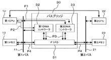
図1は、本発明の実施の形態に係わるデータ転送装置としてのバスブリッジ30の構成および接続状態を示している。第1のシステムのシステムバスである第1バス11には、第1CPU12と第1メモリ13とが接続されている。第2のシステムのシステムバスである第2バス21には、第2CPU22と第2メモリ23とが接続されている。第1バス11と第2バス21とはバスブリッジ30を介して接続されている。ここでは、第1バス11と第1CPU12は共にPCI(Peripheral Component Interconnect)バスになっている。
FIG. 1 shows the configuration and connection state of a
バスブリッジ30は、バッファメモリとしてのFIFOメモリ31と、第1DMAコントローラ32と、第2DMAコントローラ33とを備えている。第1DMAコントローラ32は、第1バス11側の第1メモリ13とFIFOメモリ31との間でのデータ転送を制御する。第2DMAコントローラ33は第2バス21側の第2メモリ23とFIFOメモリ31との間でのデータ転送を制御するものである。ここでは、第1DMAコントローラ32および第2DMAコントローラ33の内部レジスタの設定は第1バス11上の第1CPU12から行なわれる。
The
第1DMAコントローラ32は、第1バス11のアドレスバスおよびデータバスと接続されている。また第1DMAコントローラ32の各内部レジスタは第1CPU12のアドレス空間上にマッピングされており、第1CPU12は、第1バス11を通じて第1DMAコントローラ32の各種設定レジスタにアクセス可能になっている。
The
第1DMAコントローラ32は、第1メモリ13とFIFOメモリ31との間でデータ転送する際には第1バス11のバスマスタとなり、アドレス信号やライト信号、リード信号などを第1バス11に送出するようになっている。FIFOメモリ31は第1バス11のデータバスと接続されており、第1DMAコントローラ32から入力される制御信号に応じて第1バス11にデータを送出したり第1バス11上のデータを内部に取り込んだりするようになっている。
The
第2DMAコントローラ33は、第1バス11のアドレスバスとデータバスに接続されており、各内部レジスタは第1CPU12のアドレス空間上にマッピングされている。第1CPU12は、第1バス11を通じて第2DMAコントローラ33の各種設定レジスタにアクセス可能になっている。
The
また第2DMAコントローラ33は、第2バス21のアドレスバスと接続されており、第2メモリ23とFIFOメモリ31との間でデータ転送する際には第2バス21のバスマスタとなり、アドレス信号やライト信号、リード信号などを第2バス21に送出するようになっている。FIFOメモリ31は第2バス21のデータバスと接続されており、第2DMAコントローラ33から入力される制御信号に応じて第2バス21にデータを送出したり第2バス21上のデータを内部に取り込んだりするようになっている。
The
次に、第2バス21に接続された第2メモリ23から第1バス11に接続された第1メモリ13へバスブリッジ30を用いてデータ転送する際の動作を説明する。
Next, an operation when data is transferred from the
(1):第1CPU12は、転送すべきデータの第2メモリ23内での先頭アドレス(転送元アドレス)と、転送するデータサイズ(転送量)とを第2DMAコントローラ33に設定する(図1のP1)。
(1): The
(2):第1CPU12は、転送するデータを格納すべき領域の第1メモリ13内での先頭アドレス(転送先アドレス)と、格納すべきデータサイズ(転送量)とを第1DMAコントローラ32に設定する(図1のP2)。
(2): The
(3):上記(1)、(2)の設定に基づき第1DMAコントローラ32および第2DMAコントローラ33はFIFOメモリ31を制御してDMA転送を行なう。
(3): Based on the settings of (1) and (2) above, the
(4):第1DMAコントローラ32および第2DMAコントローラ33の制御により、第2バス21側の第2メモリ23からFIFOメモリ31を介して第1バス11側の第1メモリ13にデータが転送される。
(4): Data is transferred from the
このように、システム間でメモリからメモリへデータ転送するために必要なすべての設定をバスブリッジ30に対して一方のシステムのCPUから行なうので、データの転送元システムのCPUと転送先システムのCPUとの間で同期をとる必要がなくなり、データ転送に先立つ処理が簡略化され、転送速度を実質的に高速化することができる。
As described above, since all the settings necessary for data transfer from memory to memory between systems are performed from the CPU of one system to the
転送すべきデータの第2メモリ23内での格納アドレスを第2CPU22が管理し、必要なデータがどこに格納されているかを第1CPU12が知らない場合には、第2CPU22が転送元アドレスや転送量を第2DMAコントローラ33に設置しなければならない。しかしながら、第2メモリ23から第1メモリ13に転送すべきデータの第2メモリ23内での格納アドレスを予め取り決めておけば、第1CPU12が第2メモリ23側のアドレス(転送元アドレス)等を第2DMAコントローラ33に設定することができる。本発明はこのような場合に好適である。
When the
たとえば、フレームメモリに格納された画像データを第2メモリ23から第1メモリ13に転送するような場合、フレームメモリ内の各ページの先頭アドレスを予め取り決めておけば、一方のCPUがバスブリッジ30の第1DMAコントローラ32および第2DMAコントローラ33の双方に対してデータ転送に必要なすべての情報を設定することができる。これにより、データの転送元システムのCPUと転送先システムのCPUとの間で同期をとる必要がなくなり、処理が効率化され、実質的な高速化が実現される。
For example, when image data stored in the frame memory is transferred from the
以上、本発明の実施の形態を図面によって説明してきたが、具体的な構成は実施の形態に示したものに限られるものではなく、本発明の要旨を逸脱しない範囲における変更や追加があっても本発明に含まれる。たとえば、FIFOメモリ31と第1DMAコントローラ32と第2DMAコントローラ33とを一組としたものを1つのバスブリッジ30に複数組内蔵してもよい。この場合、システム間でのデータ転送の方向を組毎に固定的に定めるとよい。
The embodiment of the present invention has been described with reference to the drawings. However, the specific configuration is not limited to that shown in the embodiment, and there are changes and additions within the scope of the present invention. Are also included in the present invention. For example, a plurality of sets of
また実施の形態では、転送先システムのCPUからデータ転送に必要なすべての情報をバスブリッジ30に設定するように構成したが、転送元システムのCPUが設定するように構成してもよい。
In the embodiment, all the information necessary for data transfer is set in the
バッファメモリはFIFOメモリに限定されず、転送されるデータを一時的に格納可能なメモリであればよい。また実施の形態では、PCIバスとPCIバスとをバスブリッジで接続する場合を例に説明したが、他の種類のバスを接続するものであってもかまわない。 The buffer memory is not limited to the FIFO memory, and may be any memory that can temporarily store transferred data. In the embodiment, the case where the PCI bus and the PCI bus are connected by a bus bridge has been described as an example. However, other types of buses may be connected.
11…第1バス
12…第1CPU
13…第1メモリ
21…第2バス
22…第2CPU
23…第2メモリ
30…バスブリッジ
31…FIFOメモリ
32…第1DMAコントローラ
33…第2DMAコントローラ
11 ...
13 ...
23 ...
Claims (3)
転送元アドレス、転送先アドレス、転送量など転送に必要な情報の設定を一方のシステムから行なう
ことを特徴とするデータ転送装置の設定方法。 For data transfer devices that transfer data from memory to memory of different and independent systems,
A method for setting a data transfer apparatus, wherein information necessary for transfer such as a transfer source address, a transfer destination address, and a transfer amount is set from one system.
転送元アドレス、転送先アドレス、転送量など転送に必要な情報を一方のシステムから設定可能に構成した
ことを特徴とするデータ転送装置。 In a data transfer device for transferring data from a memory of a different and independent system to the memory,
A data transfer apparatus characterized in that information necessary for transfer such as a transfer source address, a transfer destination address, and a transfer amount can be set from one system.
バッファメモリと、
前記バッファメモリと第1のシステムに接続されたメモリとの間でデータ転送する第1転送手段と、
前記バッファメモリと第2のシステムに接続されたメモリとの間でデータ転送する第2転送手段と
を備え、
転送元アドレス、転送先アドレス、転送量など転送に必要な情報を一方のシステムから前記第1転送手段と第2転送手段とに設定可能に構成した
ことを特徴とするデータ転送装置。
In a data transfer device for transferring data from a memory of a different and independent system to the memory,
Buffer memory,
First transfer means for transferring data between the buffer memory and a memory connected to the first system;
A second transfer means for transferring data between the buffer memory and a memory connected to the second system;
A data transfer apparatus characterized in that information necessary for transfer, such as a transfer source address, a transfer destination address, and a transfer amount, can be set from one system to the first transfer means and the second transfer means.
Priority Applications (1)
| Application Number | Priority Date | Filing Date | Title |
|---|---|---|---|
| JP2004110622A JP2005293435A (en) | 2004-04-05 | 2004-04-05 | Data transfer device and its setting method |
Applications Claiming Priority (1)
| Application Number | Priority Date | Filing Date | Title |
|---|---|---|---|
| JP2004110622A JP2005293435A (en) | 2004-04-05 | 2004-04-05 | Data transfer device and its setting method |
Publications (1)
| Publication Number | Publication Date |
|---|---|
| JP2005293435A true JP2005293435A (en) | 2005-10-20 |
Family
ID=35326265
Family Applications (1)
| Application Number | Title | Priority Date | Filing Date |
|---|---|---|---|
| JP2004110622A Withdrawn JP2005293435A (en) | 2004-04-05 | 2004-04-05 | Data transfer device and its setting method |
Country Status (1)
| Country | Link |
|---|---|
| JP (1) | JP2005293435A (en) |
Cited By (4)
| Publication number | Priority date | Publication date | Assignee | Title |
|---|---|---|---|---|
| JP2007299116A (en) * | 2006-04-28 | 2007-11-15 | Fuji Xerox Co Ltd | Image processor |
| JP2013205928A (en) * | 2012-03-27 | 2013-10-07 | Fujitsu Semiconductor Ltd | Semiconductor integrated circuit and dma control method thereof |
| CN112749112A (en) * | 2020-12-31 | 2021-05-04 | 无锡众星微系统技术有限公司 | Hardware flow structure |
| US11321249B2 (en) | 2018-03-26 | 2022-05-03 | Samsung Electronics Co., Ltd. | Mechanism to autonomously manage SSDS in an array |
-
2004
- 2004-04-05 JP JP2004110622A patent/JP2005293435A/en not_active Withdrawn
Cited By (8)
| Publication number | Priority date | Publication date | Assignee | Title |
|---|---|---|---|---|
| JP2007299116A (en) * | 2006-04-28 | 2007-11-15 | Fuji Xerox Co Ltd | Image processor |
| JP2013205928A (en) * | 2012-03-27 | 2013-10-07 | Fujitsu Semiconductor Ltd | Semiconductor integrated circuit and dma control method thereof |
| US9323700B2 (en) | 2012-03-27 | 2016-04-26 | Socionext Inc. | Semiconductor integrated circuit and DMA control method of the same |
| US11321249B2 (en) | 2018-03-26 | 2022-05-03 | Samsung Electronics Co., Ltd. | Mechanism to autonomously manage SSDS in an array |
| US11775454B2 (en) | 2018-03-26 | 2023-10-03 | Samsung Electronics Co., Ltd. | Mechanism to autonomously manage SSDs in an array |
| US12174762B2 (en) | 2018-03-26 | 2024-12-24 | Samsung Electronics Co., Ltd. | Mechanism to autonomously manage SSDs in an array |
| CN112749112A (en) * | 2020-12-31 | 2021-05-04 | 无锡众星微系统技术有限公司 | Hardware flow structure |
| CN112749112B (en) * | 2020-12-31 | 2021-12-24 | 无锡众星微系统技术有限公司 | Hardware flow structure |
Similar Documents
| Publication | Publication Date | Title |
|---|---|---|
| US7418537B2 (en) | Deadlock avoidance in a bus fabric | |
| JP2004171209A (en) | Shared memory data transfer device | |
| JP2001521246A (en) | Buffering data exchanged between buses operating at different frequencies | |
| US6253275B1 (en) | Interrupt gating method for PCI bridges | |
| JP2005353041A (en) | Bus transaction management within data processing system | |
| JP2005293435A (en) | Data transfer device and its setting method | |
| US7340553B2 (en) | Data processing device and method for transferring data | |
| JP5360594B2 (en) | DMA transfer apparatus and method | |
| JP2006293927A (en) | Direct memory access control device and system LSI including direct memory access control device | |
| JP2006285872A (en) | Multi CPU system | |
| JP2000227895A (en) | Device and method for transferring image data | |
| JPH09223103A (en) | Information processing system | |
| JP2002215562A (en) | DMA control apparatus and method | |
| JP2007226374A (en) | Data processing device | |
| JPS63292356A (en) | DMA control device | |
| KR19990071122A (en) | Multiprocessor circuit | |
| JP2820054B2 (en) | Bus interface device | |
| JP2638505B2 (en) | Bus interface device | |
| JPS61224063A (en) | data transfer control device | |
| JP2008198119A (en) | Data transfer device, data transfer system, and data transfer method | |
| JPH07334453A (en) | Memory access system | |
| JP2006229862A (en) | Image forming apparatus | |
| JPS6228874A (en) | Data transfer system | |
| JP2004326814A (en) | Image processing apparatus and image processing system | |
| JP2010033314A (en) | Bus access circuit device and bus access method |
Legal Events
| Date | Code | Title | Description |
|---|---|---|---|
| A300 | Withdrawal of application because of no request for examination |
Free format text: JAPANESE INTERMEDIATE CODE: A300 Effective date: 20070605 |