JP2005292242A - Imaging apparatus and method for manufacturing the same - Google Patents

Imaging apparatus and method for manufacturing the same Download PDF

Info

Publication number
JP2005292242A
JP2005292242A JP2004103754A JP2004103754A JP2005292242A JP 2005292242 A JP2005292242 A JP 2005292242A JP 2004103754 A JP2004103754 A JP 2004103754A JP 2004103754 A JP2004103754 A JP 2004103754A JP 2005292242 A JP2005292242 A JP 2005292242A
Authority
JP
Japan
Prior art keywords
imaging
circuit board
unit
lens
optical system
Prior art date
Legal status (The legal status is an assumption and is not a legal conclusion. Google has not performed a legal analysis and makes no representation as to the accuracy of the status listed.)
Pending
Application number
JP2004103754A
Other languages
Japanese (ja)
Inventor
Takahiko Yagi
能彦 八木
Tomoaki Kuroishi
友明 黒石
Current Assignee (The listed assignees may be inaccurate. Google has not performed a legal analysis and makes no representation or warranty as to the accuracy of the list.)
Panasonic Holdings Corp
Original Assignee
Matsushita Electric Industrial Co Ltd
Priority date (The priority date is an assumption and is not a legal conclusion. Google has not performed a legal analysis and makes no representation as to the accuracy of the date listed.)
Filing date
Publication date
Application filed by Matsushita Electric Industrial Co Ltd filed Critical Matsushita Electric Industrial Co Ltd
Priority to JP2004103754A priority Critical patent/JP2005292242A/en
Publication of JP2005292242A publication Critical patent/JP2005292242A/en
Pending legal-status Critical Current

Links

Images

Abstract

<P>PROBLEM TO BE SOLVED: To accurately determine a distance between an optical system of an imaging apparatus and an image pickup surface and the inclination of the optical system from the image pickup surface. <P>SOLUTION: The imaging apparatus 1 is provided with an image pickup part 2, a 3-dimensional circuit board 3 on which the image pickup part 2 is packaged, a lens part 4 for guiding incident light into the image pickup part 2, and a lens holding part 5. The lens holding part 5 is mounted on the 3-dimensional circuit board 3 while performing positioning by engaging a lens position reference hole 52a with a lens position reference part 36a and engaging the other lens position reference hole with the other lens position reference part. When a plurality of first reference surfaces 361 of the solid circuit board 3 are abutted on a plurality of second reference surfaces 521 of the lens holding part 5, the distance between a lens part 4 held by the lens holding part 5 and the image pickup surface 211 of the image pickup part 2 accurately mounted on the circuit substrate 3 and the inclination of the lens part 4 from the image pickup surface 211 can be accurately determined. <P>COPYRIGHT: (C)2006,JPO&NCIPI

Description

本発明は、撮像装置およびその製造方法に関する。   The present invention relates to an imaging device and a manufacturing method thereof.

従来より、ビデオカメラや携帯型電話機用カメラ等の撮像装置を小型化するために、CCD(Charge Coupled device)チップ等の撮像素子が用いられている。例えば、特許文献1では、ガラス基板上実装されたCCDチップを、抵抗器等が内蔵された多層セラミック基板のパッケージにより覆う技術が開示されている。   2. Description of the Related Art Conventionally, an imaging device such as a CCD (Charge Coupled Device) chip has been used to reduce the size of an imaging device such as a video camera or a mobile phone camera. For example, Patent Document 1 discloses a technique in which a CCD chip mounted on a glass substrate is covered with a multilayer ceramic substrate package in which a resistor or the like is built.

近年、このような撮像装置に対して、装置の小型化に加えて撮像精度の向上が求められており、撮像素子に光を導くレンズと撮像素子との位置合わせを高精度に行うための様々な技術が提案されている。例えば、撮像素子が実装された回路基板上にレンズを保持する鏡筒を紫外線硬化樹脂を介して仮配置し、鏡筒を微小移動させつつ焦点合わせを行い、焦点が合った時点で紫外線を照射して鏡筒を回路基板上に固定する方法が知られている。   In recent years, in addition to downsizing the apparatus, improvement in imaging accuracy has been demanded for such an imaging apparatus, and there are various methods for accurately aligning a lens that guides light to the imaging element and the imaging element. Technologies have been proposed. For example, a lens barrel that holds a lens on a circuit board on which an image sensor is mounted is temporarily placed via an ultraviolet curable resin. Focusing is performed while the lens barrel is moved slightly, and ultraviolet rays are irradiated when the focus is achieved. A method of fixing the lens barrel on the circuit board is known.

特許文献2では、レンズが嵌め込まれた立体プリント基板に撮像素子を実装することにより、撮像素子とレンズの光軸との位置ずれを少なくする技術が開示されている。特許文献3では、立体プリント基板の撮像素子収容部およびレンズマウント部に撮像素子およびレンズを取り付けることにより、撮像素子の中心とレンズの光学中心(光軸)との位置合わせを精度良く実現する技術が開示されている。   Patent Document 2 discloses a technique for reducing the positional deviation between the imaging element and the optical axis of the lens by mounting the imaging element on a three-dimensional printed board in which the lens is fitted. In Patent Document 3, a technique for accurately realizing alignment between the center of the image sensor and the optical center (optical axis) of the lens by attaching the image sensor and the lens to the image sensor housing portion and the lens mount portion of the three-dimensional printed circuit board. Is disclosed.

また、特許文献4では、撮像素子を含む集積回路が実装される立体プリント基板の端子部を集積回路のバンプに当接させることによりレンズの光軸方向において弾性変形させ、その状態で接着剤を注入して集積回路を固定する技術が開示されている。また、このとき、位置決め用の突起により集積回路の光軸方向位置のセッティングを容易とする手法も開示されている。
特開平6−5828号公報 特開2001−245186号公報 特開2002−280535号公報 特開2001−333332号公報
In Patent Document 4, the terminal portion of the three-dimensional printed circuit board on which the integrated circuit including the image sensor is mounted is brought into contact with the bump of the integrated circuit to be elastically deformed in the optical axis direction of the lens. A technique for injecting and fixing an integrated circuit is disclosed. At this time, a technique is also disclosed that facilitates setting of the position of the integrated circuit in the optical axis direction by the positioning protrusions.
JP-A-6-5828 JP 2001-245186 A JP 2002-280535 A JP 2001-333332 A

ところで、撮像装置の撮像精度を向上させるためには、レンズの光軸に垂直な平面におけるレンズの光軸と撮像素子との相対位置を合わせるだけではなく、光軸方向におけるレンズと撮像素子の撮像面との間の距離も精度良く決定する必要がある。また、レンズと撮像面とが平行になるように、撮像面に対するレンズの傾きを精度良く決定する必要もある。   By the way, in order to improve the imaging accuracy of the imaging device, not only aligning the relative position of the optical axis of the lens and the imaging element in a plane perpendicular to the optical axis of the lens, but also imaging of the lens and the imaging element in the optical axis direction. It is also necessary to determine the distance between the surfaces with high accuracy. In addition, it is necessary to accurately determine the inclination of the lens with respect to the imaging surface so that the lens and the imaging surface are parallel to each other.

しかしながら、特許文献1に開示される装置では、レンズ以外の部分の小型化はなされるものの、レンズを含めた小型化およびレンズと撮像素子との相対的な位置関係に対する対策についてはなされていない。また、特許文献2に開示される装置では、レンズおよび撮像素子が同一の胴部に取り付けられるため、レンズと撮像素子との間の距離をある程度精度よく決定することができるが、レンズの取付と撮像素子の実装とが1つの胴部に対して行われるため、装置製造工程の管理が煩雑となる。   However, in the apparatus disclosed in Patent Document 1, although parts other than the lens are miniaturized, no measures are taken for miniaturization including the lens and relative positional relationship between the lens and the image sensor. In addition, in the apparatus disclosed in Patent Document 2, since the lens and the image sensor are attached to the same body, the distance between the lens and the image sensor can be determined with a certain degree of accuracy. Since the mounting of the image sensor is performed on one body part, management of the apparatus manufacturing process becomes complicated.

一方、特許文献3に開示される装置では、光軸に垂直な平面におけるレンズの光軸と撮像素子との位置合わせを精度良く行うことができるが、レンズを保持するレンズキャップの内周全体がレンズ筒部の外周に嵌め合わされるため、レンズキャップとレンズ筒部との間に接着剤が挟まる等の原因でレンズ筒部の上面とレンズキャップの対向面とが非接触状態となり、レンズの撮像面からの距離を精度よく決定することができなくなってしまう。   On the other hand, the apparatus disclosed in Patent Document 3 can accurately align the optical axis of the lens and the imaging element in a plane perpendicular to the optical axis, but the entire inner circumference of the lens cap that holds the lens is Since it is fitted on the outer periphery of the lens barrel, the upper surface of the lens barrel and the opposite surface of the lens cap are in a non-contact state due to an adhesive being sandwiched between the lens cap and the lens barrel. The distance from the surface cannot be determined with high accuracy.

特許文献4に開示される装置では、特許文献2の場合と同じく、装置製造工程の管理が煩雑となる。なお、レンズによる像の形成状態を測定しながら集積回路とレンズとの間の距離や集積回路の傾きを調整した場合は、レンズと集積回路との位置関係を理想的なものとすることができるが、集積回路実装時のこのような制御は煩雑であることから、撮像装置の製造に時間がかかることとなる。また、レンズを保持する鏡筒を回路基板に対して位置決めしつつ紫外線硬化樹脂を介して接合する手法が採用される場合においても、同様の煩雑な制御が必要となり、製造に時間を要することとなる。   In the apparatus disclosed in Patent Document 4, as in Patent Document 2, management of the device manufacturing process becomes complicated. Note that when the distance between the integrated circuit and the lens and the inclination of the integrated circuit are adjusted while measuring the image formation state by the lens, the positional relationship between the lens and the integrated circuit can be idealized. However, since such control when the integrated circuit is mounted is complicated, it takes time to manufacture the imaging device. In addition, even when a method of joining the lens barrel holding the lens via the ultraviolet curable resin while being positioned with respect to the circuit board is adopted, the same complicated control is required, and the manufacturing takes time. Become.

本発明は、上記課題に鑑みなされたものであり、撮像装置の光学系と撮像面との間の距離、および、光学系の撮像面に対する傾きを容易に精度良く決定することを目的としている。   The present invention has been made in view of the above problems, and an object of the present invention is to easily and accurately determine the distance between the optical system and the imaging surface of the imaging apparatus and the inclination of the optical system with respect to the imaging surface.

請求項1に記載の発明は、撮像装置であって、撮像面を有する撮像部と、前記撮像部が実装される回路基板と、入射した光を前記撮像部の前記撮像面に導く光学系と、前記光学系を保持するとともに前記回路基板に取り付けられた光学系保持部とを備え、前記回路基板が、前記撮像面に平行な第1基準面を備え、前記光学系保持部が、前記第1基準面に当接することにより、前記光学系の前記回路基板からの距離、および、前記回路基板に対する傾きを決定する第2基準面を備える。   The invention according to claim 1 is an imaging apparatus, wherein an imaging unit having an imaging surface, a circuit board on which the imaging unit is mounted, an optical system that guides incident light to the imaging surface of the imaging unit, and An optical system holding unit that holds the optical system and is attached to the circuit board, the circuit board includes a first reference plane parallel to the imaging surface, and the optical system holding unit includes the first A second reference surface that determines a distance from the circuit board of the optical system and an inclination with respect to the circuit board by contacting the reference surface.

請求項2に記載の発明は、請求項1に記載の撮像装置であって、前記回路基板が、前記第1基準面に垂直な第3基準面をさらに備え、前記光学系保持部が、前記第3基準面に当接することにより、前記回路基板に対する前記光学系の光軸の位置を決定する第4基準面をさらに備える。   The invention according to claim 2 is the imaging apparatus according to claim 1, wherein the circuit board further includes a third reference surface perpendicular to the first reference surface, and the optical system holding unit is A fourth reference surface is further provided for determining the position of the optical axis of the optical system with respect to the circuit board by contacting the third reference surface.

請求項3に記載の発明は、請求項1または2に記載の撮像装置であって、前記回路基板が、前記撮像部と当接して、前記回路基板上の前記撮像部が実装される面と前記撮像面との間の距離、および、前記回路基板に対する前記撮像面の傾きを決定する実装基準面をさらに備える。   Invention of Claim 3 is an imaging device of Claim 1 or 2, Comprising: The surface by which the said circuit board contacts the said imaging part, and the said imaging part on the said circuit board is mounted, It further includes a mounting reference plane that determines a distance between the imaging plane and an inclination of the imaging plane with respect to the circuit board.

請求項4に記載の発明は、請求項1ないし3のいずれかに記載の撮像装置であって、前記撮像部が、前記回路基板に実装されるガラス基板と、前記撮像面を有し、前記撮像面を前記ガラス基板に対向させて前記ガラス基板に実装される撮像デバイスとを備える。   Invention of Claim 4 is an imaging device in any one of Claim 1 thru | or 3, Comprising: The said imaging part has the glass substrate mounted in the said circuit board, and the said imaging surface, An imaging device mounted on the glass substrate with an imaging surface facing the glass substrate.

請求項5に記載の発明は、請求項1ないし4のいずれかに記載の撮像装置であって、前記回路基板が、前記光学系の光軸に沿って貫通する開口部をさらに備え、前記開口部内に前記撮像部の少なくとも一部を配置しつつ前記撮像部が実装される。   The invention according to claim 5 is the imaging apparatus according to any one of claims 1 to 4, wherein the circuit board further includes an opening penetrating along an optical axis of the optical system, and the opening The imaging unit is mounted while disposing at least a part of the imaging unit in the unit.

請求項6に記載の発明は、請求項1ないし5のいずれかに記載の撮像装置であって、前記回路基板が、前記回路基板上の前記撮像部が実装される面とは反対側の面に、前記撮像部の電極部と電気的に接続される配線をさらに備える。   A sixth aspect of the present invention is the imaging apparatus according to any one of the first to fifth aspects, wherein the circuit board is a surface opposite to a surface on which the imaging unit on the circuit board is mounted. In addition, a wiring electrically connected to the electrode part of the imaging part is further provided.

請求項7に記載の発明は、請求項1ないし6のいずれかに記載の撮像装置であって、前記回路基板が、モールド成形された立体回路基板である。   A seventh aspect of the present invention is the imaging apparatus according to any one of the first to sixth aspects, wherein the circuit board is a molded three-dimensional circuit board.

請求項8に記載の発明は、請求項6または7に記載の撮像装置であって、前記回路基板の前記光学系とは反対側の面に接続されるもう1つの回路基板と、前記撮像部の前記撮像面とは反対側の領域において前記光学系の光軸に沿って前記回路基板または前記もう1つの回路基板に実装され、前記撮像部からの信号を処理する電子部品とをさらに備える。   The invention according to claim 8 is the imaging apparatus according to claim 6 or 7, wherein the circuit board is connected to another surface of the circuit board opposite to the optical system, and the imaging unit. And an electronic component that is mounted on the circuit board or the other circuit board along the optical axis of the optical system in a region opposite to the imaging surface, and that processes a signal from the imaging unit.

請求項9に記載の発明は、撮像装置の製造方法であって、a) 撮像面を有する撮像部を回路基板に実装する工程と、b) 前記撮像面に平行な前記回路基板の第1基準面を、入射した光を前記撮像面に導く光学系を保持する光学系保持部の第2基準面に当接することにより、前記光学系の前記回路基板からの距離、および、前記回路基板に対する傾きを決定しつつ前記光学系保持部を前記回路基板に取り付ける工程とを備える。   The invention according to claim 9 is a method for manufacturing an imaging device, wherein a) a step of mounting an imaging unit having an imaging surface on a circuit board, and b) a first reference of the circuit board parallel to the imaging surface. The surface is brought into contact with the second reference surface of the optical system holding unit that holds the optical system that guides incident light to the imaging surface, so that the distance of the optical system from the circuit board and the inclination with respect to the circuit board And attaching the optical system holding part to the circuit board while determining.

請求項10に記載の発明は、請求項9に記載の撮像装置の製造方法であって、c) 前記a)工程と前記b)工程との間に、前記回路基板を撮像して前記回路基板に対する前記光学系の光軸の位置を決定する工程をさらに備える。   Invention of Claim 10 is a manufacturing method of the imaging device of Claim 9, Comprising: The said circuit board is imaged between the said a) process and the said b) process, and the said circuit board Determining the position of the optical axis of the optical system relative to.

請求項11に記載の発明は、請求項9または10に記載の撮像装置の製造方法であって、前記a)工程の前に、d) 前記撮像面を有する撮像デバイスを、前記撮像面を対向させてガラス基板に実装して前記撮像部を組み立てる工程をさらに備え、前記a)工程において、前記ガラス基板と前記回路基板とが接合される。   Invention of Claim 11 is a manufacturing method of the imaging device of Claim 9 or 10, Comprising: Before the said a) process, d) The imaging device which has the said imaging surface is opposed to the said imaging surface And mounting on the glass substrate to assemble the imaging unit, and in the step a), the glass substrate and the circuit board are joined.

本発明では、光学系と撮像面との間の距離、および、光学系の撮像面に対する傾きを容易に精度良く決定することができる。請求項2および10の発明では、光学系の光軸の撮像面に対する相対位置を精度良く決定することができる。請求項3の発明では、光学系と撮像面との間の距離、および、光学系の撮像面に対する傾きをさらに精度良く決定することができる。   In the present invention, the distance between the optical system and the imaging surface and the inclination of the optical system with respect to the imaging surface can be easily determined with high accuracy. According to the second and tenth aspects of the present invention, the relative position of the optical axis of the optical system with respect to the imaging surface can be determined with high accuracy. In the invention of claim 3, the distance between the optical system and the imaging surface and the inclination of the optical system with respect to the imaging surface can be determined with higher accuracy.

また、請求項4および11の発明では、撮像デバイスの回路基板への実装を容易かつ精度良く行うことができる。請求項5の発明では、撮像装置を薄型化することができる。請求項6の発明では、撮像装置を他の基板に容易に実装することができる。請求項7の発明では、撮像装置を構成する部品点数を削減するとともに、撮像装置の製造工程を簡素化することができる。請求項8の発明では、撮像装置の光軸に沿う方向における投影面積を縮小することができる。   In the inventions of claims 4 and 11, the imaging device can be mounted on the circuit board easily and accurately. In the invention of claim 5, the imaging device can be thinned. In the invention of claim 6, the imaging device can be easily mounted on another substrate. In the invention of claim 7, the number of parts constituting the imaging apparatus can be reduced and the manufacturing process of the imaging apparatus can be simplified. In the invention of claim 8, the projected area in the direction along the optical axis of the imaging device can be reduced.

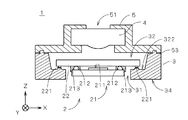
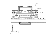
図1は、本発明の第1の実施の形態に係る撮像装置1の構成を示す正面図であり、一部を断面にて示している。撮像装置1は、撮像面211を有する撮像部2、撮像部2が実装されるモールド成形された立体回路基板(MID(Molded Interconnect Device))3、入射した光を撮像部2に導くレンズ部4、および、レンズ部4を保持するとともに立体回路基板3に取り付けられたレンズ保持部5を備える。   FIG. 1 is a front view showing a configuration of the imaging apparatus 1 according to the first embodiment of the present invention, and shows a part thereof in cross section. The imaging device 1 includes an imaging unit 2 having an imaging surface 211, a molded circuit board (MID (Molded Interconnect Device)) 3 on which the imaging unit 2 is mounted, and a lens unit 4 that guides incident light to the imaging unit 2. And a lens holding part 5 that holds the lens part 4 and is attached to the three-dimensional circuit board 3.

撮像部2は、立体回路基板3に実装されるガラス基板22、および、撮像面211を有するCCDチップ等の撮像デバイス21を備える。撮像デバイス21は、メッキにより形成されたメッキバンプ、または、ワイヤボンディング法により形成されたスタッドバンプ(以下、単に「バンプ」という。)212を備え、ガラス基板22の(−Z)側の主面に撮像面211を対向させてガラス基板22の金電極上にバンプ212を介してフリップチップ実装される。撮像デバイス21の周囲は封止剤213により封止されている。また、ガラス基板22は立体回路基板3の電極と接合される金のバンプ221を備え、バンプ221の(−Z)側の先端はZ方向に対して垂直な平面になるように予め精度良く押し潰されている(いわゆる、レベリングが施されている。)。   The imaging unit 2 includes a glass substrate 22 mounted on the three-dimensional circuit board 3 and an imaging device 21 such as a CCD chip having an imaging surface 211. The imaging device 21 includes a plated bump formed by plating or a stud bump (hereinafter simply referred to as “bump”) 212 formed by a wire bonding method, and the main surface of the glass substrate 22 on the (−Z) side. The image pickup surface 211 is opposed to the gold electrode of the glass substrate 22 so as to be flip-chip mounted via the bumps 212. The periphery of the imaging device 21 is sealed with a sealant 213. Further, the glass substrate 22 includes gold bumps 221 bonded to the electrodes of the three-dimensional circuit board 3, and the tip on the (−Z) side of the bumps 221 is accurately pressed in advance so as to be a plane perpendicular to the Z direction. It is crushed (so-called leveling is applied).

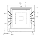
立体回路基板3は、ポリフタルアミド(PPA)樹脂により形成され、底部にZ方向に沿って貫通する開口部31が設けられる凹部32を備える。図2は、撮像部2および立体回路基板3を示す平面図である。図2に示すように、立体回路基板3の表面には配線33が設けられる。配線33は、モールド成形された基板の表面上に無電解メッキ(または、蒸着)により形成された銅薄膜に対して、配線として残置する部位とそれ以外の部位との境界線(配線33のエッジ)をレーザでパターニングすることにより両部位を電気的に分離させ、残置する部位のみに電解メッキを施した後に全面エッチングを行うことにより形成される。なお、図2では図示の便宜上、配線33の数を実際より少なく描いている。   The three-dimensional circuit board 3 is formed of polyphthalamide (PPA) resin and includes a recess 32 provided with an opening 31 penetrating along the Z direction at the bottom. FIG. 2 is a plan view showing the imaging unit 2 and the three-dimensional circuit board 3. As shown in FIG. 2, wiring 33 is provided on the surface of the three-dimensional circuit board 3. The wiring 33 is a boundary line (an edge of the wiring 33) between a portion to be left as a wiring and a portion other than the copper thin film formed by electroless plating (or vapor deposition) on the surface of the molded substrate. ) By patterning with a laser, both parts are electrically separated, and the entire part is etched after electrolytic plating is performed only on the remaining part. In FIG. 2, for the sake of illustration, the number of wires 33 is smaller than the actual number.

撮像部2は、図1に示すように、撮像部2の一部である撮像デバイス21を開口部31内に配置しつつ凹部32の底面322に実装され、バンプ221を介して配線33(図2参照)と電気的に接続される。立体回路基板3は、撮像部2が実装される底面322とは反対側の面(立体回路基板3の(−Z)側の面)34に、配線33と電気的に接続される配線をさらに備える。すなわち、撮像デバイス21は、バンプ212を介してガラス基板22上に設けられる配線に電気的に接続され、さらに、撮像部2の電極部であるバンプ221、配線33、および、面34に設けられる配線を介して撮像装置1の外部の回路基板等と電気的に接続される。なお、図1では、ガラス基板22および立体回路基板3に形成される配線の図示を省略している。   As shown in FIG. 1, the imaging unit 2 is mounted on the bottom surface 322 of the recess 32 while arranging the imaging device 21 that is a part of the imaging unit 2 in the opening 31, and the wiring 33 (FIG. 2). The three-dimensional circuit board 3 further includes a wiring electrically connected to the wiring 33 on a surface (surface on the (−Z) side of the three-dimensional circuit board 3) opposite to the bottom surface 322 on which the imaging unit 2 is mounted. Prepare. That is, the imaging device 21 is electrically connected to the wiring provided on the glass substrate 22 via the bump 212, and further provided on the bump 221, the wiring 33, and the surface 34 that are the electrode portions of the imaging unit 2. It is electrically connected to an external circuit board or the like of the imaging device 1 through wiring. In FIG. 1, illustration of wirings formed on the glass substrate 22 and the three-dimensional circuit board 3 is omitted.

レンズ部4は、撮像デバイス21の撮像面211に被写体の像を形成するレンズ群、および、赤外線の透過を防止する赤外線フィルタを備え、レンズ保持部5の中央部にZ方向に沿って設けられた貫通部内に保持される。レンズ保持部5は、レンズ部4の光軸がZ方向に沿うように(すなわち、撮像面211に垂直になるように)立体回路基板3の(+Z)側に接着剤53により固着されている。撮像装置1では、レンズ保持部5の(+Z)側の開口51からレンズ部4に入射した光が、ガラス基板22を透過して撮像デバイス21の撮像面211に導かれる。   The lens unit 4 includes a lens group that forms an image of a subject on the imaging surface 211 of the imaging device 21 and an infrared filter that prevents transmission of infrared rays. The lens unit 4 is provided at the center of the lens holding unit 5 along the Z direction. Held in the penetrating part. The lens holding unit 5 is fixed to the (+ Z) side of the three-dimensional circuit board 3 with an adhesive 53 so that the optical axis of the lens unit 4 is along the Z direction (that is, perpendicular to the imaging surface 211). . In the imaging device 1, light incident on the lens unit 4 from the (+ Z) side opening 51 of the lens holding unit 5 passes through the glass substrate 22 and is guided to the imaging surface 211 of the imaging device 21.

なお、撮像装置1では、レンズ部4に赤外線フィルタが設けられる代わりに、ガラス基板22に赤外線の透過を防止するコーティング等の加工が施されてもよい。また、図1では図示を簡略化しているが、実際にはレンズ保持部5は複数の部材からなり、これらの部材を組み合わせることでレンズ部4を保持した状態とされて予め準備される。   In the imaging device 1, instead of providing the lens unit 4 with an infrared filter, the glass substrate 22 may be subjected to processing such as coating for preventing infrared transmission. Although the illustration is simplified in FIG. 1, the lens holding portion 5 is actually composed of a plurality of members, and the lens portion 4 is held in advance by combining these members.

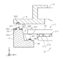
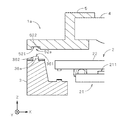
図3は、立体回路基板3上の撮像部2およびレンズ保持部5が取り付けられる部位(取付部)近傍を拡大して示す図である。図3では、図示の都合上、撮像部2、レンズ保持部5および立体回路基板3の(−X)側の部位のそれぞれを分離して示している。なお、図3に示すこれらの構成の形状は、後述のレンズ位置基準穴52を除いて左右(X方向において)対称とされる。なお、撮像面211の中心が撮像デバイス21の中心からずらして設けられている場合等、図3に示す構成が左右対称にならない場合もある。   FIG. 3 is an enlarged view showing the vicinity of the part (attachment part) to which the imaging unit 2 and the lens holding part 5 are attached on the three-dimensional circuit board 3. In FIG. 3, for convenience of illustration, the imaging unit 2, the lens holding unit 5, and the (−X) side portion of the three-dimensional circuit board 3 are separately illustrated. The shapes of these configurations shown in FIG. 3 are symmetrical (in the X direction) except for a lens position reference hole 52 described later. In some cases, such as when the center of the imaging surface 211 is shifted from the center of the imaging device 21, the configuration illustrated in FIG.

図3に示すように、立体回路基板3の凹部32の底面322には(+Z)側に突出する突起部35が設けられ(突起部35は、バンプ221の配列に合わせてY方向に長く形成されてもよく、各バンプ221に個別に対向するように同一の高さで複数個形成されてもよい。)、突起部35の(+Z)側の端面351は、Z方向に対して垂直(以下、「水平」という。)になるように精度良く形成されており、撮像部2と接合される電極がその上に設けられる。撮像部2が立体回路基板3に実装される際には、端面351が撮像部2のバンプ221に当接することにより、立体回路基板3の底面322と撮像面211との間の距離、および、立体回路基板3の底面322に対する撮像面211の傾きが決定されることから、以下、端面351を「実装基準面」という。撮像部2は、撮像面211が水平になるように立体回路基板3に実装される。   As shown in FIG. 3, the bottom surface 322 of the concave portion 32 of the three-dimensional circuit board 3 is provided with a protruding portion 35 protruding to the (+ Z) side (the protruding portion 35 is formed to be long in the Y direction according to the arrangement of the bumps 221. The plurality of bumps 221 may be formed at the same height so as to face each bump 221 individually.) (+ Z) side end surface 351 of projection 35 is perpendicular to the Z direction ( Hereinafter, it is formed with high precision so as to be “horizontal”), and an electrode joined to the imaging unit 2 is provided thereon. When the imaging unit 2 is mounted on the three-dimensional circuit board 3, the end surface 351 comes into contact with the bump 221 of the imaging unit 2, so that the distance between the bottom surface 322 of the three-dimensional circuit board 3 and the imaging surface 211, and Since the inclination of the imaging surface 211 with respect to the bottom surface 322 of the three-dimensional circuit board 3 is determined, the end surface 351 is hereinafter referred to as a “mounting reference surface”. The imaging unit 2 is mounted on the three-dimensional circuit board 3 so that the imaging surface 211 is horizontal.

立体回路基板3は、凹部32の周囲の水平な面(以下、「上面」という。)360上に3つの円柱状の突起部であるレンズ位置基準部36a〜36c(実際には図2に示すように配置される。)を備え、レンズ位置基準部36a〜36cのぞれぞれは、(+Z)側の端面361、および、端面361に垂直な側面362を備える。端面361は水平、すなわち、立体回路基板3の実装基準面351、および、立体回路基板3に実装された撮像部2の撮像面211に平行になるように精度良く形成されている。   The three-dimensional circuit board 3 has lens position reference parts 36a to 36c (actually shown in FIG. 2) which are three cylindrical protrusions on a horizontal surface (hereinafter referred to as “upper surface”) 360 around the recess 32. Each of the lens position reference parts 36a to 36c includes a (+ Z) side end surface 361 and a side surface 362 perpendicular to the end surface 361. The end surface 361 is formed with high accuracy so as to be horizontal, that is, parallel to the mounting reference surface 351 of the 3D circuit board 3 and the imaging surface 211 of the imaging unit 2 mounted on the 3D circuit board 3.

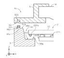
図4は、レンズ保持部5を(−Z)側から(+Z)方向を向いて見た底面図である。図3および図4に示すように、レンズ保持部5は、レンズ位置基準部36a,36bとの嵌め合いにより立体回路基板3に対するレンズ保持部5の相対的な位置が決定される2つのレンズ位置基準穴52a,52bおよびレンズ位置基準部36cが挿入されるレンズ位置基準穴52cを(−Z)側の面に備える。(−X)側のレンズ位置基準穴52aは、レンズ位置基準部36aと等しい直径を有する円柱状とされ、Z方向の深さはレンズ位置基準部36aの高さより小さくされる。また、(+X)側のレンズ位置基準穴52bは、レンズ保持部5の立体回路基板3に対する取り付けを適切に行うために、Y方向の幅がレンズ位置基準部36bの直径と等しいX方向に長い長穴となっており、深さはレンズ位置基準穴52aと等しくされる。(+Y)側のレンズ位置基準穴52cは直径がレンズ位置基準部36cよりも十分に大きく、深さはレンズ位置基準穴52aと等しくされる。   FIG. 4 is a bottom view of the lens holding unit 5 as viewed from the (−Z) side in the (+ Z) direction. As shown in FIGS. 3 and 4, the lens holding unit 5 has two lens positions in which the relative position of the lens holding unit 5 with respect to the three-dimensional circuit board 3 is determined by fitting with the lens position reference units 36 a and 36 b. A lens position reference hole 52c into which the reference holes 52a and 52b and the lens position reference portion 36c are inserted is provided on the (−Z) side surface. The lens position reference hole 52a on the (−X) side has a cylindrical shape having the same diameter as the lens position reference portion 36a, and the depth in the Z direction is smaller than the height of the lens position reference portion 36a. Further, the lens position reference hole 52b on the (+ X) side is long in the X direction so that the width in the Y direction is equal to the diameter of the lens position reference part 36b in order to appropriately attach the lens holding part 5 to the three-dimensional circuit board 3. It is a long hole, and the depth is made equal to the lens position reference hole 52a. The lens position reference hole 52c on the (+ Y) side is sufficiently larger in diameter than the lens position reference portion 36c, and the depth is made equal to the lens position reference hole 52a.

図3に示すように、レンズ位置基準穴52aは、(+Z)側の底面521および側面522を備える。底面521はレンズ保持部5に保持されるレンズ部4の光軸に対して垂直になるように精度良く形成され、側面522は底面521に対して垂直になるように精度よく形成される。レンズ位置基準穴52bも精度よく形成された底面521および側面522を備え、レンズ位置基準穴52cは底面521のみが精度よく形成される。   As shown in FIG. 3, the lens position reference hole 52 a includes a bottom surface 521 and a side surface 522 on the (+ Z) side. The bottom surface 521 is accurately formed so as to be perpendicular to the optical axis of the lens unit 4 held by the lens holding unit 5, and the side surface 522 is formed accurately so as to be perpendicular to the bottom surface 521. The lens position reference hole 52b also includes a bottom surface 521 and a side surface 522 formed with high accuracy, and only the bottom surface 521 of the lens position reference hole 52c is formed with high accuracy.

レンズ保持部5が立体回路基板3に取り付けられる際には、レンズ位置基準穴52a〜52cの底面521がレンズ位置基準部36a〜36cの端面361に当接することにより、レンズ保持部5に保持されるレンズ部4の立体回路基板3からの距離、および、立体回路基板3に対する傾きが決定される。以下、レンズ位置基準部36の端面361、および、レンズ位置基準穴52の底面521をそれぞれ、「第1基準面」361および「第2基準面」521という。   When the lens holding unit 5 is attached to the three-dimensional circuit board 3, the bottom surfaces 521 of the lens position reference holes 52a to 52c are held by the lens holding unit 5 by contacting the end surfaces 361 of the lens position reference units 36a to 36c. The distance of the lens unit 4 from the three-dimensional circuit board 3 and the inclination of the three-dimensional circuit board 3 are determined. Hereinafter, the end surface 361 of the lens position reference unit 36 and the bottom surface 521 of the lens position reference hole 52 are referred to as a “first reference surface” 361 and a “second reference surface” 521, respectively.

また、レンズ位置基準穴52aの側面522のほぼ全周がレンズ位置基準部36aの側面362に当接し、レンズ位置基準穴52bの側面522の(±Y)側の部位がレンズ位置基準部36bの側面362に当接することにより、立体回路基板3に対するレンズ部4の光軸の水平方向の位置が決定されることから、以下、レンズ位置基準部36a,36bの側面362、および、レンズ位置基準穴52a,52bの側面522をそれぞれ、「第3基準面」362および「第4基準面」522という。   Further, almost the entire circumference of the side surface 522 of the lens position reference hole 52a is in contact with the side surface 362 of the lens position reference portion 36a, and the (± Y) side portion of the side surface 522 of the lens position reference hole 52b is the lens position reference portion 36b. Since the horizontal position of the optical axis of the lens unit 4 with respect to the three-dimensional circuit board 3 is determined by contacting the side surface 362, the side surfaces 362 of the lens position reference units 36a and 36b, and the lens position reference hole will be described below. The side surfaces 522 of 52a and 52b are referred to as “third reference plane” 362 and “fourth reference plane” 522, respectively.

図5は、撮像装置1の製造工程を示す図である。撮像装置1が製造される際には、まず、図3に示すガラス基板22の(−Z)側の主面が上に向けられた状態で、バンプ212がガラス基板22の電極に当接するように撮像デバイス21が載置され、撮像デバイス21がガラス基板22に対して押圧されつつ超音波振動が付与されることにより、バンプ212とガラス基板22の電極とが電気的に接合される。これにより、撮像デバイス21が撮像面211をガラス基板22の(−Z)側の主面に平行に対向させてガラス基板22に実装(いわゆる、フリップチップ実装)される(ステップS11)。なお、撮像デバイス21のガラス基板22への実装は、クリーンレベルの高い環境下にて行われ、かつ、フリップチップ実装装置を用いて非常に精度よく行われる。   FIG. 5 is a diagram illustrating a manufacturing process of the imaging device 1. When the imaging apparatus 1 is manufactured, first, the bump 212 is brought into contact with the electrode of the glass substrate 22 with the main surface on the (−Z) side of the glass substrate 22 shown in FIG. The imaging device 21 is mounted on the glass substrate 22, and ultrasonic vibration is applied while the imaging device 21 is pressed against the glass substrate 22, whereby the bump 212 and the electrode of the glass substrate 22 are electrically joined. Thereby, the imaging device 21 is mounted on the glass substrate 22 (so-called flip chip mounting) with the imaging surface 211 facing the main surface on the (−Z) side of the glass substrate 22 in parallel (step S11). The mounting of the imaging device 21 on the glass substrate 22 is performed in an environment with a high clean level, and is performed with high accuracy using a flip chip mounting apparatus.

続いて、撮像デバイス21とガラス基板22との間の隙間に光硬化性樹脂等を含む封止剤213が注入され、予め撮像面211を含む撮像デバイス21の中央部の領域にガラス基板22を介して照射されている光により、封止剤213が撮像面211に到達する前に撮像デバイス21の周辺部において硬化し、撮像デバイス21とガラス基板22との間の隙間が封止され、撮像面211が外気から遮断される(ステップS12)。このように、撮像部2では、ガラス基板22を利用することにより撮像面211が容易に封止され、以後の製造工程における撮像面211に対するダストや湿気等の影響(特に、後述するガラス基板22の立体回路基板3への実装時、および、レンズ保持部5の立体回路基板3への取り付け時における影響)を容易に排除することができる。また、光を透過する封止剤が用いられる場合には、撮像面211を含めて撮像デバイス21とガラス基板22との間の隙間の全ての領域に封止剤が注入されて撮像面211が封止されてもよい。   Subsequently, a sealant 213 containing a photocurable resin or the like is injected into the gap between the imaging device 21 and the glass substrate 22, and the glass substrate 22 is placed in a central region of the imaging device 21 including the imaging surface 211 in advance. The sealant 213 is cured at the peripheral portion of the imaging device 21 before reaching the imaging surface 211 by the light irradiated through the imaging device 21, and the gap between the imaging device 21 and the glass substrate 22 is sealed. The surface 211 is shielded from outside air (step S12). As described above, in the imaging unit 2, the imaging surface 211 is easily sealed by using the glass substrate 22, and the influence of dust, moisture, etc. on the imaging surface 211 in the subsequent manufacturing process (particularly, the glass substrate 22 described later). (Effect of mounting the lens holding portion 5 on the three-dimensional circuit board 3) and the mounting of the lens holding part 5 on the three-dimensional circuit board 3 can be easily eliminated. When a sealant that transmits light is used, the sealant is injected into all regions of the gap between the image pickup device 21 and the glass substrate 22 including the image pickup surface 211, so that the image pickup surface 211 is formed. It may be sealed.

撮像部2が準備されると、次に、図3に示すように立体回路基板3の実装基準面351の電極上に導電性粒子が内部に均一に分散された絶縁性樹脂により形成される異方導電性樹脂フィルム(以下、「ACF(Anisotropic Conductive Film)」という。)352が貼り付けられる。続いて、立体回路基板3に設けられたアライメントマークが撮像され、撮像により取得された画像データに基づいて撮像部2の立体回路基板3に対する位置決めが行われた後、撮像部2がACF352上から押圧されて加熱される。これにより、立体回路基板3に撮像部2が固着されるとともにバンプ221が実装基準面351上の電極と電気的に接合され、立体回路基板3に撮像部2が実装される(ステップS13)。   When the imaging unit 2 is prepared, next, as shown in FIG. 3, the conductive particles are formed on the electrodes of the mounting reference surface 351 of the three-dimensional circuit board 3 by an insulating resin in which the conductive particles are uniformly dispersed. A directionally conductive resin film (hereinafter referred to as “ACF (Anisotropic Conductive Film)”) 352 is attached. Subsequently, after the alignment mark provided on the three-dimensional circuit board 3 is imaged and the image pickup unit 2 is positioned with respect to the three-dimensional circuit board 3 based on the image data acquired by the image pickup, the image pickup unit 2 is moved from above the ACF 352. Pressed and heated. Thereby, the imaging unit 2 is fixed to the three-dimensional circuit board 3 and the bumps 221 are electrically joined to the electrodes on the mounting reference surface 351, and the imaging unit 2 is mounted on the three-dimensional circuit board 3 (step S13).

このとき、バンプ221の(−Z)側の面と実装基準面351との間においてACF352は1μm〜2μm(マイクロメートル)の厚さまで押しつぶされ、ガラス基板22の(−Z)側の主面が実装基準面351と平行になるように精度良く実装される。撮像面211も実装基準面351に平行となり、また、撮像面211の立体回路基板3からの距離(例えば、基準位置を立体回路基板3の底面322とした場合、撮像面211と底面322との間の距離)が精度良く決定される。なお、撮像部2の実装時における加熱温度は、撮像デバイス21の耐熱温度(通常、180℃程度)を考慮して決定される。   At this time, the ACF 352 is crushed between the (−Z) side surface of the bump 221 and the mounting reference surface 351 to a thickness of 1 μm to 2 μm (micrometer), and the (−Z) side main surface of the glass substrate 22 is It is mounted with high accuracy so as to be parallel to the mounting reference plane 351. The imaging surface 211 is also parallel to the mounting reference surface 351, and the distance of the imaging surface 211 from the three-dimensional circuit board 3 (for example, when the reference position is the bottom surface 322 of the three-dimensional circuit board 3, the imaging surface 211 and the bottom surface 322 are The distance between them is determined with high accuracy. Note that the heating temperature when mounting the imaging unit 2 is determined in consideration of the heat-resistant temperature of the imaging device 21 (usually about 180 ° C.).

撮像部2の立体回路基板3への実装が完了すると、立体回路基板3のレンズ位置基準部36を除く上面360上に接着剤53が塗布される。続いて、レンズ部4を保持したレンズ保持部5が、レンズ位置基準穴52a〜52cとレンズ位置基準部36a〜36cとを嵌め合わせることにより位置決めが行われつつ立体回路基板3に取り付けられる(ステップS14)。   When the mounting of the imaging unit 2 on the three-dimensional circuit board 3 is completed, the adhesive 53 is applied on the upper surface 360 of the three-dimensional circuit board 3 excluding the lens position reference unit 36. Subsequently, the lens holding part 5 holding the lens part 4 is attached to the three-dimensional circuit board 3 while being positioned by fitting the lens position reference holes 52a to 52c and the lens position reference parts 36a to 36c (step). S14).

このとき、既述のように3つのレンズ位置基準部36a〜36cの第1基準面361と3つのレンズ位置基準穴52a〜52cの第2基準面521とが当接することにより、第2基準面521に垂直なレンズ部4の光軸は第1基準面361に対しても垂直となり、レンズ保持部5に保持されるレンズ部4の立体回路基板3に対する傾きが精度良く決定される。また、レンズ部4の立体回路基板3からの距離(例えば、レンズ部4の(−Z)側の端部と立体回路基板3の底面322との間のZ方向の距離)が精度良く決定される。さらに、レンズ位置基準部36a,36bの第3基準面362とレンズ位置基準穴52a,52bの第4基準面522とが当接することにより、レンズ部4の光軸の立体回路基板3に対するXY平面における相対位置が精度良く決定される。その後、接着剤53が硬化してレンズ保持部5が立体回路基板3に固定されて撮像装置1の製造が完了する。   At this time, as described above, the first reference surface 361 of the three lens position reference portions 36a to 36c and the second reference surface 521 of the three lens position reference holes 52a to 52c come into contact with each other, whereby the second reference surface. The optical axis of the lens unit 4 perpendicular to 521 is also perpendicular to the first reference plane 361, and the inclination of the lens unit 4 held by the lens holding unit 5 with respect to the three-dimensional circuit board 3 is accurately determined. Further, the distance of the lens unit 4 from the three-dimensional circuit board 3 (for example, the distance in the Z direction between the (−Z) side end of the lens unit 4 and the bottom surface 322 of the three-dimensional circuit board 3) is accurately determined. The Further, the third reference surface 362 of the lens position reference portions 36a and 36b and the fourth reference surface 522 of the lens position reference holes 52a and 52b come into contact with each other, whereby the XY plane of the optical axis of the lens portion 4 with respect to the three-dimensional circuit board 3 is obtained. The relative position at is accurately determined. Thereafter, the adhesive 53 is cured, and the lens holding unit 5 is fixed to the three-dimensional circuit board 3 to complete the manufacture of the imaging device 1.

以上に説明したように、撮像装置1では、レンズ保持部5を立体回路基板3に取り付ける際に、第1基準面361と第2基準面521とを当接することにより、レンズ保持部5に保持されるレンズ部4と立体回路基板3に精度良く実装された撮像部2の撮像面211との間の距離、および、レンズ部4の撮像面211に対する傾きを容易に、すなわち、複雑な制御を伴うことなく、精度良く決定することができる。また、第3基準面362と第4基準面522とを当接することにより、撮像面211に対するレンズ部4の光軸の水平方向の相対位置を精度良く決定することができる。   As described above, in the imaging device 1, when the lens holding unit 5 is attached to the three-dimensional circuit board 3, the first reference surface 361 and the second reference surface 521 are brought into contact with each other to be held by the lens holding unit 5. The distance between the lens unit 4 and the imaging surface 211 of the imaging unit 2 mounted on the three-dimensional circuit board 3 with high accuracy and the inclination of the lens unit 4 with respect to the imaging surface 211 can be easily controlled, that is, complicated control can be performed. It is possible to determine with high accuracy without accompanying. Further, by bringing the third reference surface 362 and the fourth reference surface 522 into contact with each other, the horizontal relative position of the optical axis of the lens unit 4 with respect to the imaging surface 211 can be accurately determined.

さらに、撮像装置1では、撮像部2が第1基準面361に平行な実装基準面351に当接して立体回路基板3に精度良く実装されることにより、レンズ部4と撮像面211との間の距離、および、レンズ部4の撮像面211に対する傾きをさらに精度良く決定することができる。また、平面度が高いガラス基板22を介して撮像デバイス21を立体回路基板3に実装することにより、撮像デバイス21の立体回路基板3への実装を容易かつ精度良く行うことができる。これにより、撮像面211とレンズ部4との相対的位置関係の精度を容易に向上することができる。さらには、ガラス基板22の熱膨張係数(約8×10⁻⁶/℃)は樹脂基板の熱膨張係数(約25×10−6/℃)に比べて小さいため、撮像デバイス21の接合部への熱応力を小さくすることができ、撮像デバイス21の接合信頼性を向上することができる。   Further, in the imaging device 1, the imaging unit 2 is mounted on the three-dimensional circuit board 3 with high accuracy by contacting the mounting reference surface 351 parallel to the first reference surface 361, so that the lens unit 4 and the imaging surface 211 are arranged. And the inclination of the lens unit 4 with respect to the imaging surface 211 can be determined with higher accuracy. Further, by mounting the imaging device 21 on the three-dimensional circuit board 3 through the glass substrate 22 having high flatness, the imaging device 21 can be mounted on the three-dimensional circuit board 3 easily and accurately. Thereby, the precision of the relative positional relationship of the imaging surface 211 and the lens part 4 can be improved easily. Furthermore, since the thermal expansion coefficient (about 8 × 10 −6 / ° C.) of the glass substrate 22 is smaller than the thermal expansion coefficient (about 25 × 10 −6 / ° C.) of the resin substrate, to the joint portion of the imaging device 21. Thus, the thermal stress of the imaging device 21 can be improved.

なお、撮像デバイス21とガラス基板22との間は必ずしも樹脂を用いて完全に封止される必要はなく、完全な封止が行われない場合であっても撮像デバイス21とガラス基板22とが近接するため、ステップS13以降の撮像装置1の製造環境のクリーンレベルを極めて高く設定する必要はない。   Note that the image pickup device 21 and the glass substrate 22 do not necessarily need to be completely sealed using a resin, and the image pickup device 21 and the glass substrate 22 are not completely sealed even when complete sealing is not performed. Since they are close to each other, it is not necessary to set the clean level of the manufacturing environment of the imaging device 1 after step S13 to be extremely high.

撮像装置1では、立体回路基板3がモールド成形されているため、撮像装置1を構成する部品点数を削減するとともに立体回路基板3の寸法精度を向上することができ、撮像装置1の製造工程を簡素化することができる。また、撮像デバイス21を立体回路基板3の開口部31内に配置しつつ撮像部2が立体回路基板3に実装されることにより、撮像装置1を薄型化(レンズ部4の光軸に沿うZ方向の高さを小さく)することができる。さらには、立体回路基板3の面34に撮像部2と電気的に接続される配線が設けられるため、面34を介して撮像装置1を他の基板に容易に実装することができる。   In the imaging device 1, since the three-dimensional circuit board 3 is molded, the number of components constituting the imaging device 1 can be reduced and the dimensional accuracy of the three-dimensional circuit board 3 can be improved. It can be simplified. Further, the imaging device 2 is mounted on the three-dimensional circuit board 3 while the imaging device 21 is disposed in the opening 31 of the three-dimensional circuit board 3, thereby reducing the thickness of the imaging device 1 (Z along the optical axis of the lens unit 4). Direction height). Furthermore, since the wiring 34 electrically connected to the imaging unit 2 is provided on the surface 34 of the three-dimensional circuit board 3, the imaging device 1 can be easily mounted on another substrate via the surface 34.

図6は、第2の実施の形態に係る撮像装置1aの立体回路基板3の取付部近傍を拡大して示す図である。撮像装置1aでは、第1の実施の形態に係る撮像装置1の3つのレンズ位置基準穴52a〜52cの形状が変更される点を除いて図3とほぼ同様であり、以下の説明において同符号を付す。   FIG. 6 is an enlarged view showing the vicinity of the attachment portion of the three-dimensional circuit board 3 of the imaging device 1a according to the second embodiment. The imaging apparatus 1a is substantially the same as FIG. 3 except that the shapes of the three lens position reference holes 52a to 52c of the imaging apparatus 1 according to the first embodiment are changed. Is attached.

撮像装置1aでは、3つのレンズ位置基準穴52a〜52cの形状(図6ではレンズ位置基準穴52aのみを図示)は、レンズ位置基準部36a〜36c(レンズ位置基準部36aのみ図示)よりも大きい直径を有する同一の円柱状とされ、Z方向の深さはレンズ位置基準部36a〜36cの高さより小さくされる。なお、図3の場合と異なり、各レンズ位置基準部36a〜36cの側面362および各レンズ位置基準穴52a〜52cの側面522の精度は余り高くはされない(すなわち、これらの側面は既述の第3基準面や第4基準面としては利用されない。)。   In the imaging device 1a, the shape of the three lens position reference holes 52a to 52c (only the lens position reference hole 52a is shown in FIG. 6) is larger than the lens position reference parts 36a to 36c (only the lens position reference part 36a is shown). The same cylindrical shape having a diameter is formed, and the depth in the Z direction is made smaller than the height of the lens position reference portions 36a to 36c. Unlike the case of FIG. 3, the accuracy of the side surfaces 362 of the lens position reference portions 36a to 36c and the side surfaces 522 of the lens position reference holes 52a to 52c is not so high (that is, these side surfaces are the same as those described above. It is not used as the third reference plane or the fourth reference plane.)

撮像装置1aの製造工程では、図5に示す撮像装置1の製造工程と同様に、撮像デバイス21がガラス基板22に実装されて封止された後、ガラス基板22が立体回路基板3に実装されるが(ステップS11〜S13)、その後のステップS14に係る工程が異なる。ステップS14では、まず、立体回路基板3に設けられたアライメントマークが撮像され、撮像により取得された画像データに基づいてレンズ保持部5に保持されるレンズ部4の光軸の立体回路基板3に対する位置(XY平面における位置)が決定された後、レンズ位置基準穴52a〜52cにレンズ位置基準部36a〜36cが挿入され、レンズ位置基準部36a〜36cの端面である第1基準面361とレンズ位置基準穴52a〜52cの底面である第2基準面521とが当接するようにレンズ保持部5が立体回路基板3に取り付けられる。   In the manufacturing process of the imaging device 1a, the imaging device 21 is mounted on the glass substrate 22 and sealed, and then the glass substrate 22 is mounted on the three-dimensional circuit board 3, as in the manufacturing process of the imaging device 1 shown in FIG. However (steps S11 to S13), the subsequent steps related to step S14 are different. In step S14, first, an alignment mark provided on the three-dimensional circuit board 3 is imaged, and the optical axis of the lens unit 4 held by the lens holding unit 5 with respect to the three-dimensional circuit board 3 based on the image data acquired by the imaging. After the position (position on the XY plane) is determined, the lens position reference parts 36a to 36c are inserted into the lens position reference holes 52a to 52c, and the first reference surface 361 and the lens which are end faces of the lens position reference parts 36a to 36c. The lens holding part 5 is attached to the three-dimensional circuit board 3 so that the second reference surface 521 which is the bottom surface of the position reference holes 52a to 52c abuts.

これにより、レンズ部4と撮像部2の撮像面211との間の距離、および、レンズ部4の撮像面211に対する傾きが容易に精度良く決定される。また、アライメントマークを利用してレンズ部4の光軸の撮像面211に対する相対位置を精度良く決定することができる。なお、アライメントマークとしては立体回路基板3に形成されたスルーホールが利用されてもよい。   Thereby, the distance between the lens unit 4 and the imaging surface 211 of the imaging unit 2 and the inclination of the lens unit 4 with respect to the imaging surface 211 are easily and accurately determined. In addition, the relative position of the optical axis of the lens unit 4 with respect to the imaging surface 211 can be accurately determined using the alignment mark. As the alignment mark, a through hole formed in the three-dimensional circuit board 3 may be used.

図7は、第3の実施の形態に係る撮像装置1bの立体回路基板3の取付部近傍を拡大して示す図である。撮像装置1bでは、第1の実施の形態に係る撮像装置1からレンズ位置基準穴52a〜52c(図7ではレンズ位置基準穴52aのみを図示)の深さおよびレンズ位置基準部36a〜36c(レンズ位置基準部36aのみを図示)の高さが変更されており、また、突起部35に代えて突起部35bが設けられ、撮像部2のガラス基板22には、バンプ221に代えてボールバンプ221bが設けられる。その他の構成は図3と同様であり、以下の説明において同符号を付す。   FIG. 7 is an enlarged view showing the vicinity of the attachment portion of the three-dimensional circuit board 3 of the imaging device 1b according to the third embodiment. In the imaging apparatus 1b, the depth of the lens position reference holes 52a to 52c (only the lens position reference hole 52a is shown in FIG. 7) and the lens position reference parts 36a to 36c (lens) from the imaging apparatus 1 according to the first embodiment. The height of only the position reference portion 36a is changed), and a projection 35b is provided instead of the projection 35, and the glass substrate 22 of the imaging unit 2 has a ball bump 221b instead of the bump 221. Is provided. Other configurations are the same as those in FIG. 3, and the same reference numerals are given in the following description.

レンズ位置基準部36a〜36cおよびレンズ位置基準穴52a〜52cは、撮像装置1に係るもの(図2および図4参照)と同じ横断面の形状を有するが、図7に示すようにレンズ位置基準穴52a〜52cの深さがレンズ位置基準部36a〜36cの高さより大きくされる。また、立体回路基板3の上面360、および、レンズ保持部5が立体回路基板3に取り付けられる際に上面360に対向する面(以下、「取付面」という。)54は、Z方向に対して垂直になるように精度良く平坦に形成されている。   The lens position reference portions 36a to 36c and the lens position reference holes 52a to 52c have the same cross-sectional shape as that related to the imaging device 1 (see FIGS. 2 and 4), but as shown in FIG. The depth of the holes 52a to 52c is made larger than the height of the lens position reference portions 36a to 36c. Further, the upper surface 360 of the three-dimensional circuit board 3 and a surface (hereinafter referred to as “attachment surface”) 54 facing the upper surface 360 when the lens holding unit 5 is attached to the three-dimensional circuit board 3 are in the Z direction. It is formed accurately and flat so as to be vertical.

撮像装置1bでは、レンズ保持部5が立体回路基板3に取り付けられる際には、レンズ位置基準部36a〜36cの(+Z)側の端面に接着剤53が塗布された後にレンズ位置基準部36a〜36cとレンズ位置基準穴52a〜52cとが嵌め合わされる。このとき、立体回路基板3の上面360とレンズ保持部5の取付面54とが当接することにより、レンズ保持部5に保持されるレンズ部4の立体回路基板3からの距離、および、立体回路基板3に対する傾きが容易に精度良く決定される。すなわち、上面360および取付面54はそれぞれ、レンズ部4の立体回路基板3からの距離、および、立体回路基板3に対する傾きを決定する第1基準面および第2基準面としての役割を果たす。その結果、レンズ部4と立体回路基板3に精度良く実装された撮像部2の撮像面211との間の距離、および、レンズ部4の撮像面211に対する傾きを精度良く決定することができる。   In the imaging device 1b, when the lens holding part 5 is attached to the three-dimensional circuit board 3, the lens position reference part 36a to 36a is applied after the adhesive 53 is applied to the (+ Z) side end surfaces of the lens position reference parts 36a to 36c. 36c and the lens position reference holes 52a to 52c are fitted together. At this time, when the upper surface 360 of the three-dimensional circuit board 3 and the mounting surface 54 of the lens holding unit 5 abut, the distance from the three-dimensional circuit board 3 of the lens unit 4 held by the lens holding unit 5 and the three-dimensional circuit The inclination with respect to the substrate 3 is easily determined with high accuracy. That is, the upper surface 360 and the mounting surface 54 serve as a first reference surface and a second reference surface that determine the distance of the lens unit 4 from the three-dimensional circuit board 3 and the inclination with respect to the three-dimensional circuit board 3, respectively. As a result, the distance between the lens unit 4 and the imaging surface 211 of the imaging unit 2 mounted on the three-dimensional circuit board 3 with high accuracy and the inclination of the lens unit 4 with respect to the imaging surface 211 can be determined with high accuracy.

また、図3の撮像装置1の場合と同様に、レンズ位置基準部36a,36bの側面である第3基準面362とレンズ位置基準穴52a,52bの側面である第4基準面522とが当接することによって、レンズ保持部5に保持されるレンズ部4の光軸の立体回路基板3に対する水平方向の相対位置が精度良く決定される。   Similarly to the case of the imaging device 1 of FIG. 3, the third reference surface 362 which is the side surface of the lens position reference portions 36a and 36b and the fourth reference surface 522 which is the side surface of the lens position reference holes 52a and 52b are matched. By contact, the relative position in the horizontal direction of the optical axis of the lens unit 4 held by the lens holding unit 5 with respect to the three-dimensional circuit board 3 is accurately determined.

図7に示すように、突起部35bは、立体回路基板3の凹部32の底面322上において、撮像部2のボールバンプ221bが接合される部位から外れた位置に設けられ、その上面には電極は形成されない。撮像装置1bにおいて撮像部2が立体回路基板3に実装される際には、底面322の電極上に塗布された銀ペースト等の導電性接着剤上からボールバンプ221bを介してガラス基板22が立体回路基板3に対して押圧される。このとき、ボールバンプ221bが押圧力により変形する(押し潰される)ことによってガラス基板22が突起部35bの(+Z)側の端面である実装基準面351に当接する。この状態で接着剤の硬化が行われ、撮像部2が立体回路基板3に固定される。ガラス基板22を実装基準面351に当接させることにより、撮像部2が立体回路基板3に精度良く実装され、レンズ部4と撮像面211との間の距離、および、レンズ部4の撮像面211に対する傾きをさらに精度良く決定することができる。   As shown in FIG. 7, the protrusion 35 b is provided on the bottom surface 322 of the concave portion 32 of the three-dimensional circuit board 3 at a position away from the portion to which the ball bump 221 b of the imaging unit 2 is joined. Is not formed. When the imaging unit 2 is mounted on the three-dimensional circuit board 3 in the imaging device 1b, the glass substrate 22 is three-dimensionally formed on the conductive adhesive such as silver paste applied on the electrode of the bottom surface 322 via the ball bumps 221b. Pressed against the circuit board 3. At this time, when the ball bump 221b is deformed (crushed) by the pressing force, the glass substrate 22 comes into contact with the mounting reference surface 351 which is the end surface on the (+ Z) side of the protruding portion 35b. In this state, the adhesive is cured, and the imaging unit 2 is fixed to the three-dimensional circuit board 3. By bringing the glass substrate 22 into contact with the mounting reference surface 351, the imaging unit 2 is accurately mounted on the three-dimensional circuit board 3, the distance between the lens unit 4 and the imaging surface 211, and the imaging surface of the lens unit 4. The inclination with respect to 211 can be determined with higher accuracy.

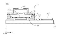
図8は、撮像装置1が回路基板6に実装された撮像ユニット10の構成を示す正面図であり、一部を断面にて示している。撮像ユニット10は、第1の実施の形態に係る撮像装置1、撮像装置1の立体回路基板3の(−Z)側(レンズ部4とは反対側)の面34に接続される平板状の回路基板6(フィルム状の回路基板であってもよい。)、撮像装置1の撮像部2からの信号を処理するDSP(Digital Signal Processor)チップ等の電子部品61、および、コンデンサや抵抗等の複数の周辺チップ部品62を備える。撮像装置1の構成は図1と同様であり、以下の説明において同符号を付す。なお、図8では、図示の都合上、周辺チップ部品62を1つのみ描いている。   FIG. 8 is a front view showing the configuration of the imaging unit 10 in which the imaging device 1 is mounted on the circuit board 6, and a part thereof is shown in cross section. The imaging unit 10 is a flat plate connected to the surface 34 on the (−Z) side (opposite side of the lens unit 4) of the imaging device 1 according to the first embodiment and the three-dimensional circuit board 3 of the imaging device 1. An electronic component 61 such as a circuit board 6 (may be a film-like circuit board), a DSP (Digital Signal Processor) chip that processes a signal from the imaging unit 2 of the imaging device 1, and a capacitor, a resistor, and the like A plurality of peripheral chip components 62 are provided. The configuration of the imaging apparatus 1 is the same as that in FIG. In FIG. 8, only one peripheral chip part 62 is drawn for the sake of illustration.

撮像ユニット10では、回路基板6の(+Z)側の面上にはんだを介して周辺チップ部品62および撮像装置1が実装され、電子部品61がACF等を用いて実装される。なお、撮像装置1の実装では、レンズ部4等の熱による損傷を防止するために、レーザを利用した局所加熱や回路基板6の(−Z)側からの局所加熱等により局所リフローが行われて撮像装置1と回路基板6とが接合される。また、撮像装置1は、銀ペースト等の導電性接着剤を介して低温にて接合されてもよい。電子部品61および周辺チップ部品62は、立体回路基板3および回路基板6の配線を介して撮像部2と電気的に接続される。撮像ユニット10では、レンズ部4の撮像面211からの距離、および、撮像面211に対する傾きが精度良く決定された薄型の撮像装置1が使用されるため、装置の薄型化が実現される。   In the imaging unit 10, the peripheral chip component 62 and the imaging device 1 are mounted on the (+ Z) side surface of the circuit board 6 via solder, and the electronic component 61 is mounted using ACF or the like. In mounting the imaging device 1, local reflow is performed by local heating using a laser, local heating from the (−Z) side of the circuit board 6, or the like in order to prevent damage to the lens unit 4 or the like due to heat. Thus, the imaging device 1 and the circuit board 6 are joined. Moreover, the imaging device 1 may be joined at a low temperature via a conductive adhesive such as a silver paste. The electronic component 61 and the peripheral chip component 62 are electrically connected to the imaging unit 2 via the wiring of the three-dimensional circuit board 3 and the circuit board 6. In the imaging unit 10, since the thin imaging device 1 in which the distance from the imaging surface 211 of the lens unit 4 and the inclination with respect to the imaging surface 211 are accurately determined is used, the device can be thinned.

図9は、撮像ユニットの他の例を示す正面図である。図9に示す撮像ユニット10aは、撮像ユニット10と同様の構成を備えるが、電子部品61が回路基板6の(−Z)側(回路基板6を挟んで撮像装置1とは反対側)の面に実装されている点が異なる。電子部品61は、撮像部2の撮像面211とは(撮像デバイス21の本体部214を挟んで)反対側の領域においてレンズ部4の光軸に沿って回路基板6に実装されるため、回路基板6を小型化することができ、レンズ部4の光軸に沿う方向における撮像ユニット10aの投影面積を縮小することができる。その結果、撮像ユニット10aを備える携帯型電話機等の製品を小型化することができる。なお、周辺チップ部品62も、回路基板6を挟んで撮像装置1の反対側に設けられてもよく、この場合、撮像ユニット10aの投影面積をさらに縮小することができる。なお、撮像ユニット10aが高さ方向(Z方向)に対する小型化が余り求められない場合には、撮像装置1の立体回路基板3は、必ずしもZ方向に沿って貫通する開口部31を備える必要はなく、図10に示すようにキャビティ37を備えていてもよい。   FIG. 9 is a front view illustrating another example of the imaging unit. The imaging unit 10a shown in FIG. 9 has the same configuration as that of the imaging unit 10, but the surface of the electronic component 61 on the (−Z) side of the circuit board 6 (on the side opposite to the imaging apparatus 1 with the circuit board 6 in between). Is different in that it is implemented. Since the electronic component 61 is mounted on the circuit board 6 along the optical axis of the lens unit 4 in a region opposite to the imaging surface 211 of the imaging unit 2 (with the main body 214 of the imaging device 21 sandwiched), a circuit is provided. The board | substrate 6 can be reduced in size and the projection area of the imaging unit 10a in the direction along the optical axis of the lens part 4 can be reduced. As a result, a product such as a mobile phone including the imaging unit 10a can be reduced in size. The peripheral chip component 62 may also be provided on the opposite side of the imaging device 1 with the circuit board 6 interposed therebetween. In this case, the projected area of the imaging unit 10a can be further reduced. When the imaging unit 10a is not required to be downsized in the height direction (Z direction), the three-dimensional circuit board 3 of the imaging device 1 is not necessarily provided with the opening 31 that penetrates along the Z direction. Alternatively, a cavity 37 may be provided as shown in FIG.

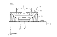
図11は、撮像ユニットのさらに他の例を示す正面図である。図11に示す撮像ユニット10bでは、撮像装置1の立体回路基板3に、図9に示す開口部31よりも深い(Z方向に長い)開口部31が設けられる。その他の構成は図9と同様であり、以下の説明において同符号を付す。撮像ユニット10bの撮像装置1では、撮像デバイス21を開口部31内に配置しつつ撮像部2が立体回路基板3に実装されている。そして、回路基板6の(+Z)側に実装された電子部品61を覆うように撮像装置1が回路基板6上に実装され、電子部品61が開口部31内に配置される。その結果、回路基板6の同一面上に電子部品61および撮像部1を実装しつつレンズ部4の光軸に沿う方向における撮像ユニット10bの投影面積を縮小することができる。   FIG. 11 is a front view showing still another example of the imaging unit. In the imaging unit 10b illustrated in FIG. 11, an opening 31 deeper (longer in the Z direction) than the opening 31 illustrated in FIG. 9 is provided in the three-dimensional circuit board 3 of the imaging device 1. Other configurations are the same as those in FIG. 9, and the same reference numerals are given in the following description. In the imaging device 1 of the imaging unit 10 b, the imaging unit 2 is mounted on the three-dimensional circuit board 3 while the imaging device 21 is disposed in the opening 31. The imaging device 1 is mounted on the circuit board 6 so as to cover the electronic component 61 mounted on the (+ Z) side of the circuit board 6, and the electronic component 61 is disposed in the opening 31. As a result, the projection area of the imaging unit 10b in the direction along the optical axis of the lens unit 4 can be reduced while mounting the electronic component 61 and the imaging unit 1 on the same surface of the circuit board 6.

図12および図13は、撮像ユニットのさらに他の例を示す正面図である。これらの撮像ユニットでは、撮像装置1の立体回路基板3に、電子部品61が実装される。   12 and 13 are front views showing still other examples of the imaging unit. In these imaging units, an electronic component 61 is mounted on the three-dimensional circuit board 3 of the imaging device 1.

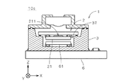
図12に示す撮像ユニット10cでは、立体回路基板3にキャビティ37が設けられ、電子部品61がキャビティ37の底面((+Z)側の面)に実装されており、撮像部2が、撮像デバイス21の一部をキャビティ37内に配置しつつ電子部品61を覆うように立体回路基板3に実装されている。電子部品61は、立体回路基板3の配線を介して撮像部2と電気的に接続されている。   In the imaging unit 10 c shown in FIG. 12, the cavity 37 is provided in the three-dimensional circuit board 3, the electronic component 61 is mounted on the bottom surface (the (+ Z) side surface) of the cavity 37, and the imaging unit 2 is connected to the imaging device 21. Is mounted on the three-dimensional circuit board 3 so as to cover the electronic component 61 while disposing a part thereof in the cavity 37. The electronic component 61 is electrically connected to the imaging unit 2 via the wiring of the three-dimensional circuit board 3.

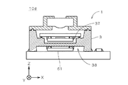
図13に示す撮像ユニット10dにおいても、立体回路基板3に(浅い)キャビティ37が設けられ、電子部品61がキャビティ37の底面の裏面((−Z)側の面)に実装される。電子部品61は、立体回路基板3の配線および底面のビアを介して撮像部2と電気的に接続されている。   Also in the imaging unit 10 d shown in FIG. 13, the (shallow) cavity 37 is provided in the three-dimensional circuit board 3, and the electronic component 61 is mounted on the back surface (the (−Z) side surface) of the bottom surface of the cavity 37. The electronic component 61 is electrically connected to the imaging unit 2 via the wiring of the three-dimensional circuit board 3 and vias on the bottom surface.

撮像ユニット10cおよび10dでは、電子部品61を立体回路基板3に実装して撮像に係る構成をスタック化することにより、電子部品61を撮像部2やレンズ部4等と一体的に取り扱うことができるため、各種電子部品等の回路基板6への実装工程を簡素化することができる。また、電子部品61が撮像部2の撮像面211とは反対側の領域においてレンズ部4の光軸に沿って立体回路基板3に実装されるため、レンズ部4の光軸に沿う方向における撮像ユニットの投影面積を縮小することができる。   In the imaging units 10c and 10d, the electronic component 61 can be handled integrally with the imaging unit 2, the lens unit 4 and the like by mounting the electronic component 61 on the three-dimensional circuit board 3 and stacking the configuration related to imaging. Therefore, it is possible to simplify the process of mounting various electronic components and the like on the circuit board 6. Further, since the electronic component 61 is mounted on the three-dimensional circuit board 3 along the optical axis of the lens unit 4 in a region opposite to the imaging surface 211 of the imaging unit 2, imaging in the direction along the optical axis of the lens unit 4 is performed. The projected area of the unit can be reduced.

以上、本発明の実施の形態について説明してきたが、本発明は上記実施の形態に限定されるものではなく、様々な変更が可能である。   As mentioned above, although embodiment of this invention has been described, this invention is not limited to the said embodiment, A various change is possible.

例えば、撮像装置の立体回路基板3は、ポリフタルアミド樹脂以外の他の材料、例えば、エポキシ樹脂やPEEK(ポリエーテル・エーテル・ケトン)樹脂、液晶ポリマー等によりモールド成形された基板であってもよい。また、セラミックの成形基板であってもよく、さらには、複数のセラミック基板を積層して焼成することにより形成された多層セラミック基板でもよい。   For example, the three-dimensional circuit board 3 of the image pickup apparatus may be a board molded by a material other than polyphthalamide resin, for example, an epoxy resin, a PEEK (polyether ether ketone) resin, a liquid crystal polymer, or the like. Good. Further, it may be a ceramic molded substrate, or may be a multilayer ceramic substrate formed by laminating and firing a plurality of ceramic substrates.

撮像部2では、撮像デバイス21のガラス基板22への実装方法は、上述のように超音波を用いる方法には限定されず、例えば、ACFや異方導電性樹脂ペースト(ACP(Anisotropic Conductive Paste))、あるいは、非導電性樹脂フィルム(NCF(Non-Conductive Film))や非導電性樹脂ペースト(NCP(Non-Conductive Paste))を介して撮像デバイス21が装着され、同時に加熱および加圧が行われてバンプ212とガラス基板22の電極とが電気的に接合されてもよい。   In the imaging unit 2, the mounting method of the imaging device 21 on the glass substrate 22 is not limited to the method using ultrasonic waves as described above. For example, ACF or anisotropic conductive resin paste (ACP (Anisotropic Conductive Paste)) ) Or the image pickup device 21 is mounted via a non-conductive resin film (NCF (Non-Conductive Film)) or a non-conductive resin paste (NCP (Non-Conductive Paste)), and heating and pressurization are performed simultaneously. In other words, the bump 212 and the electrode of the glass substrate 22 may be electrically joined.

撮像部2の立体回路基板3への実装においても、ACF352に代えてACP、NCFあるいはNCPが用いられてもよい。また、撮像部2が立体回路基板3に対して押圧されつつ超音波振動が付与されることにより、撮像部2のバンプ221と立体回路基板3の電極とが電気的に接合されてもよい。   In mounting the imaging unit 2 on the three-dimensional circuit board 3, ACP, NCF, or NCP may be used instead of the ACF 352. The bumps 221 of the imaging unit 2 and the electrodes of the 3D circuit board 3 may be electrically joined by applying ultrasonic vibration while the imaging unit 2 is pressed against the 3D circuit board 3.

レンズ保持部5の立体回路基板3に対する位置決めは、レンズ位置基準部である突起部がレンズ保持部5の(−Z)側の面に設けられ、立体回路基板3の上面360に設けられたレンズ位置基準穴と嵌め合うことにより行われてもよい。   The lens holding part 5 is positioned with respect to the three-dimensional circuit board 3 by providing a projection as a lens position reference part on the (−Z) side surface of the lens holding part 5 and a lens provided on the upper surface 360 of the three-dimensional circuit board 3. It may be performed by fitting with the position reference hole.

撮像部2では、撮像デバイス21として、例えば、CMOS(Complementary Metal Oxide Semiconductor)イメージセンサが用いられてもよい。CMOSイメージセンサのチップにDSPが形成されている場合には、撮像部2からの信号を処理する電子部品61が撮像ユニットから省略される場合もある。   In the imaging unit 2, for example, a CMOS (Complementary Metal Oxide Semiconductor) image sensor may be used as the imaging device 21. When the DSP is formed on the chip of the CMOS image sensor, the electronic component 61 that processes the signal from the imaging unit 2 may be omitted from the imaging unit.

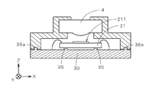
また、撮像装置1では、ガラス基板22が省略されて撮像デバイス21が撮像部2として取り扱われてもよく、また、立体回路基板3の代わりに平板状の回路基板が設けられてもよい。例えば、図14に示すように、撮像デバイス21が平板状の回路基板30上にワイヤボンディング法により直接実装されてもよい。この場合、(+Z)側の端面が水平になるように精度良く形成された突起部35が回路基板30に設けられ、撮像デバイス21が突起部35に当接して回路基板30に接着されることにより、回路基板30と撮像面211とのZ方向の位置関係が精度よく決定される。回路基板30上には、例えば、図2および図3の場合と同様のレンズ位置基準部36a〜36cも設けられ、レンズ位置基準部36a〜36cがレンズ保持部5のレンズ位置基準穴に嵌め合わされることにより、レンズ保持部5の位置決めが行われ、レンズ部4と撮像面211との間の距離、および、レンズ部4の撮像面211に対する傾きが精度良く決定される。なお、レンズ位置基準部の個数は、4以上であってもよい。   In the imaging apparatus 1, the glass substrate 22 may be omitted, and the imaging device 21 may be handled as the imaging unit 2, and a flat circuit board may be provided instead of the three-dimensional circuit board 3. For example, as shown in FIG. 14, the imaging device 21 may be directly mounted on a flat circuit board 30 by a wire bonding method. In this case, the projection part 35 formed with high precision so that the end surface on the (+ Z) side is horizontal is provided on the circuit board 30, and the imaging device 21 abuts on the projection part 35 and is bonded to the circuit board 30. Thus, the positional relationship in the Z direction between the circuit board 30 and the imaging surface 211 is determined with high accuracy. On the circuit board 30, for example, lens position reference portions 36 a to 36 c similar to those in FIGS. 2 and 3 are also provided, and the lens position reference portions 36 a to 36 c are fitted into the lens position reference holes of the lens holding portion 5. Accordingly, the lens holding unit 5 is positioned, and the distance between the lens unit 4 and the imaging surface 211 and the inclination of the lens unit 4 with respect to the imaging surface 211 are determined with high accuracy. The number of lens position reference portions may be four or more.

本発明は、携帯型電話機用カメラやビデオカメラ等に用いられる撮像装置に利用可能である。   The present invention can be used for an imaging apparatus used for a mobile phone camera, a video camera, or the like.

第1の実施の形態に係る撮像装置の構成を示す正面図1 is a front view illustrating a configuration of an imaging apparatus according to a first embodiment. 撮像部および立体回路基板を示す平面図The top view which shows an imaging part and a three-dimensional circuit board 立体回路基板の取付部近傍を拡大して示す図The figure which expands and shows the attachment part neighborhood of a three-dimensional circuit board 立体回路基板の底面図Bottom view of 3D circuit board 撮像装置の製造工程を示す図The figure which shows the manufacturing process of an imaging device 第2の実施の形態に係る撮像装置の立体回路基板の取付部近傍を拡大して示す図The figure which expands and shows the attachment part vicinity of the three-dimensional circuit board of the imaging device which concerns on 2nd Embodiment 第3の実施の形態に係る撮像装置の立体回路基板の取付部近傍を拡大して示す図The figure which expands and shows the attachment part vicinity of the three-dimensional circuit board of the imaging device which concerns on 3rd Embodiment. 撮像ユニットの構成を示す正面図Front view showing the configuration of the imaging unit 撮像ユニットの他の例を示す正面図Front view showing another example of imaging unit 撮像ユニットのさらに他の例を示す図The figure which shows the further another example of an imaging unit 撮像ユニットのさらに他の例を示す正面図Front view showing still another example of the imaging unit 撮像ユニットのさらに他の例を示す正面図Front view showing still another example of the imaging unit 撮像ユニットのさらに他の例を示す図The figure which shows the further another example of an imaging unit 撮像装置の他の例を示す図The figure which shows the other example of an imaging device

符号の説明Explanation of symbols

1,1a,1b 撮像装置
10,10a〜10d 撮像ユニット
2 撮像部
3 立体回路基板
4 レンズ部
5 レンズ保持部
6 回路基板
21 撮像デバイス
22 ガラス基板
31 開口部
34 面
61 電子部品
211 撮像面
221 バンプ
221b ボールバンプ
322 底面
351 実装基準面
361 第1基準面
362 第3基準面
521 第2基準面
522 第4基準面
S11〜S14 ステップ
DESCRIPTION OF SYMBOLS 1,1a, 1b Imaging device 10, 10a-10d Imaging unit 2 Imaging part 3 Three-dimensional circuit board 4 Lens part 5 Lens holding part 6 Circuit board 21 Imaging device 22 Glass substrate 31 Opening 34 surface 61 Electronic component 211 Imaging surface 221 Bump 221b Ball bump 322 Bottom surface 351 Mounting reference surface 361 First reference surface 362 Third reference surface 521 Second reference surface 522 Fourth reference surface S11 to S14 Steps

Claims (11)

撮像装置であって、
撮像面を有する撮像部と、
前記撮像部が実装される回路基板と、
入射した光を前記撮像部の前記撮像面に導く光学系と、
前記光学系を保持するとともに前記回路基板に取り付けられた光学系保持部と、
を備え、
前記回路基板が、前記撮像面に平行な第1基準面を備え、
前記光学系保持部が、前記第1基準面に当接することにより、前記光学系の前記回路基板からの距離、および、前記回路基板に対する傾きを決定する第2基準面を備えることを特徴とする撮像装置。
An imaging device,
An imaging unit having an imaging surface;
A circuit board on which the imaging unit is mounted;
An optical system for guiding incident light to the imaging surface of the imaging unit;
An optical system holding unit that holds the optical system and is attached to the circuit board;
With
The circuit board includes a first reference plane parallel to the imaging surface;
The optical system holding portion includes a second reference surface that determines a distance of the optical system from the circuit board and an inclination with respect to the circuit board by contacting the first reference surface. Imaging device.
請求項1に記載の撮像装置であって、
前記回路基板が、前記第1基準面に垂直な第3基準面をさらに備え、
前記光学系保持部が、前記第3基準面に当接することにより、前記回路基板に対する前記光学系の光軸の位置を決定する第4基準面をさらに備えることを特徴とする撮像装置。
The imaging apparatus according to claim 1,
The circuit board further comprises a third reference plane perpendicular to the first reference plane;
The imaging apparatus further comprising a fourth reference surface that determines a position of an optical axis of the optical system with respect to the circuit board by the optical system holding unit being in contact with the third reference surface.
請求項1または2に記載の撮像装置であって、
前記回路基板が、前記撮像部と当接して、前記回路基板上の前記撮像部が実装される面と前記撮像面との間の距離、および、前記回路基板に対する前記撮像面の傾きを決定する実装基準面をさらに備えることを特徴とする撮像装置。
The imaging apparatus according to claim 1, wherein:
The circuit board is in contact with the imaging unit to determine a distance between a surface on which the imaging unit is mounted on the circuit board and the imaging surface, and an inclination of the imaging surface with respect to the circuit board. An imaging apparatus, further comprising a mounting reference plane.
請求項1ないし3のいずれかに記載の撮像装置であって、
前記撮像部が、
前記回路基板に実装されるガラス基板と、
前記撮像面を有し、前記撮像面を前記ガラス基板に対向させて前記ガラス基板に実装される撮像デバイスと、
を備えることを特徴とする撮像装置。
The imaging apparatus according to any one of claims 1 to 3,
The imaging unit is
A glass substrate mounted on the circuit board;
An imaging device having the imaging surface and mounted on the glass substrate with the imaging surface facing the glass substrate;
An imaging apparatus comprising:
請求項1ないし4のいずれかに記載の撮像装置であって、
前記回路基板が、前記光学系の光軸に沿って貫通する開口部をさらに備え、
前記開口部内に前記撮像部の少なくとも一部を配置しつつ前記撮像部が実装されることを特徴とする撮像装置。
The imaging apparatus according to any one of claims 1 to 4,
The circuit board further comprises an opening penetrating along the optical axis of the optical system;
An imaging apparatus, wherein the imaging unit is mounted while disposing at least a part of the imaging unit in the opening.
請求項1ないし5のいずれかに記載の撮像装置であって、
前記回路基板が、前記回路基板上の前記撮像部が実装される面とは反対側の面に、前記撮像部の電極部と電気的に接続される配線をさらに備えることを特徴とする撮像装置。
The imaging apparatus according to any one of claims 1 to 5,
The image pickup apparatus, wherein the circuit board further includes a wiring electrically connected to an electrode part of the image pickup unit on a surface opposite to a surface on which the image pickup unit is mounted on the circuit board. .
請求項1ないし6のいずれかに記載の撮像装置であって、
前記回路基板が、モールド成形された立体回路基板であることを特徴とする撮像装置。
The imaging device according to any one of claims 1 to 6,
An imaging apparatus, wherein the circuit board is a molded three-dimensional circuit board.
請求項6または7に記載の撮像装置であって、
前記回路基板の前記光学系とは反対側の面に接続されるもう1つの回路基板と、
前記撮像部の前記撮像面とは反対側の領域において前記光学系の光軸に沿って前記回路基板または前記もう1つの回路基板に実装され、前記撮像部からの信号を処理する電子部品と、
をさらに備えることを特徴とする撮像装置。
The imaging device according to claim 6 or 7, wherein
Another circuit board connected to a surface of the circuit board opposite to the optical system;
An electronic component that is mounted on the circuit board or the other circuit board along the optical axis of the optical system in a region opposite to the imaging surface of the imaging unit, and that processes a signal from the imaging unit;
An image pickup apparatus further comprising:
撮像装置の製造方法であって、
a) 撮像面を有する撮像部を回路基板に実装する工程と、
b) 前記撮像面に平行な前記回路基板の第1基準面を、入射した光を前記撮像面に導く光学系を保持する光学系保持部の第2基準面に当接することにより、前記光学系の前記回路基板からの距離、および、前記回路基板に対する傾きを決定しつつ前記光学系保持部を前記回路基板に取り付ける工程と、
を備えることを特徴とする撮像装置の製造方法。
A method for manufacturing an imaging device, comprising:
a) mounting an imaging unit having an imaging surface on a circuit board;
b) contacting the first reference surface of the circuit board parallel to the imaging surface with a second reference surface of an optical system holding unit that holds an optical system that guides incident light to the imaging surface; Attaching the optical system holding part to the circuit board while determining the distance from the circuit board and the inclination with respect to the circuit board;
An image pickup apparatus manufacturing method comprising:
請求項9に記載の撮像装置の製造方法であって、
c) 前記a)工程と前記b)工程との間に、前記回路基板を撮像して前記回路基板に対する前記光学系の光軸の位置を決定する工程をさらに備えることを特徴とする撮像装置の製造方法。
It is a manufacturing method of the imaging device according to claim 9,
c) The imaging apparatus further comprising the step of imaging the circuit board and determining the position of the optical axis of the optical system with respect to the circuit board between the step a) and the step b). Production method.
請求項9または10に記載の撮像装置の製造方法であって、前記a)工程の前に、
d) 前記撮像面を有する撮像デバイスを、前記撮像面を対向させてガラス基板に実装して前記撮像部を組み立てる工程をさらに備え、
前記a)工程において、前記ガラス基板と前記回路基板とが接合されることを特徴とする撮像装置の製造方法。
It is a manufacturing method of the imaging device according to claim 9 or 10, Comprising: Before the a) process,
d) further comprising the step of assembling the imaging unit by mounting the imaging device having the imaging surface on a glass substrate with the imaging surface facing each other,
In the step a), the glass substrate and the circuit board are bonded together.
JP2004103754A 2004-03-31 2004-03-31 Imaging apparatus and method for manufacturing the same Pending JP2005292242A (en)

Priority Applications (1)

Application Number Priority Date Filing Date Title
JP2004103754A JP2005292242A (en) 2004-03-31 2004-03-31 Imaging apparatus and method for manufacturing the same

Applications Claiming Priority (1)

Application Number Priority Date Filing Date Title
JP2004103754A JP2005292242A (en) 2004-03-31 2004-03-31 Imaging apparatus and method for manufacturing the same

Publications (1)

Publication Number Publication Date
JP2005292242A true JP2005292242A (en) 2005-10-20

Family

ID=35325274

Family Applications (1)

Application Number Title Priority Date Filing Date
JP2004103754A Pending JP2005292242A (en) 2004-03-31 2004-03-31 Imaging apparatus and method for manufacturing the same

Country Status (1)

Country Link
JP (1) JP2005292242A (en)

Cited By (13)

* Cited by examiner, † Cited by third party
Publication number Priority date Publication date Assignee Title
WO2010023788A1 (en) * 2008-08-26 2010-03-04 パナソニック株式会社 Imaging device
JP2012189910A (en) * 2011-03-11 2012-10-04 Sharp Corp Camera module and manufacturing method thereof
WO2012165691A1 (en) * 2011-06-03 2012-12-06 (주)에이직뱅크 Stereoscopic image sensor package and method for manufacturing same
JP2014217033A (en) * 2013-04-30 2014-11-17 株式会社ニコン Imaging apparatus
JP2015014702A (en) * 2013-07-05 2015-01-22 株式会社ニコン Imaging unit, method for manufacturing the same and imaging device
JP2017523467A (en) * 2014-07-23 2017-08-17 ヘプタゴン・マイクロ・オプティクス・プライベート・リミテッドHeptagon Micro Optics Pte. Ltd. Luminescent body and photodetection module including vertical alignment mechanism
WO2018079644A1 (en) * 2016-10-27 2018-05-03 京セラ株式会社 Substrate for imaging element mounting, imaging device and imaging module
JP2018139455A (en) * 2018-06-15 2018-09-06 株式会社ニコン Imaging unit and imaging device
CN109328318A (en) * 2016-04-15 2019-02-12 赫普塔冈微光有限公司 Optoelectronic module with alignment spaces part and the method for assembling the optoelectronic module
JP2020101818A (en) * 2020-02-26 2020-07-02 株式会社ニコン Imaging unit and imaging device
KR102210538B1 (en) * 2020-05-08 2021-02-01 주식회사 퓨런티어 Method for manufacturing camera module
WO2021171865A1 (en) * 2020-02-26 2021-09-02 パナソニックIpマネジメント株式会社 Semiconductor laser device
US11689792B2 (en) 2020-05-08 2023-06-27 Furonteer Inc. Camera module manufacturing apparatus, camera module, and manufacturing method thereof

Citations (4)

* Cited by examiner, † Cited by third party
Publication number Priority date Publication date Assignee Title
JPH065828A (en) * 1992-06-16 1994-01-14 Sony Corp Extra-small ccd module
JPH10321825A (en) * 1997-05-15 1998-12-04 Sony Corp Assembling method for solid-state image-pickup device
JP2001308302A (en) * 2000-04-27 2001-11-02 Mitsubishi Electric Corp Image sensing device, product with image sensing device, and manufacturing method of image sensing device
JP2002077682A (en) * 2000-09-05 2002-03-15 Nikon Corp Solid state imaging device

Patent Citations (4)

* Cited by examiner, † Cited by third party
Publication number Priority date Publication date Assignee Title
JPH065828A (en) * 1992-06-16 1994-01-14 Sony Corp Extra-small ccd module
JPH10321825A (en) * 1997-05-15 1998-12-04 Sony Corp Assembling method for solid-state image-pickup device
JP2001308302A (en) * 2000-04-27 2001-11-02 Mitsubishi Electric Corp Image sensing device, product with image sensing device, and manufacturing method of image sensing device
JP2002077682A (en) * 2000-09-05 2002-03-15 Nikon Corp Solid state imaging device

Cited By (25)

* Cited by examiner, † Cited by third party
Publication number Priority date Publication date Assignee Title
WO2010023788A1 (en) * 2008-08-26 2010-03-04 パナソニック株式会社 Imaging device
JP2012189910A (en) * 2011-03-11 2012-10-04 Sharp Corp Camera module and manufacturing method thereof
US8810722B2 (en) 2011-03-11 2014-08-19 Sharp Kabushiki Kaisha Camera module lens holder
WO2012165691A1 (en) * 2011-06-03 2012-12-06 (주)에이직뱅크 Stereoscopic image sensor package and method for manufacturing same
JP2014217033A (en) * 2013-04-30 2014-11-17 株式会社ニコン Imaging apparatus
JP2015014702A (en) * 2013-07-05 2015-01-22 株式会社ニコン Imaging unit, method for manufacturing the same and imaging device
US10566363B2 (en) 2014-07-23 2020-02-18 Heptagon Micro Optics Pte. Ltd. Light emitter and light detector modules including vertical alignment features
KR102282827B1 (en) * 2014-07-23 2021-07-28 에이엠에스 센서스 싱가포르 피티이. 리미티드. Light emitter and light detector modules including vertical alignment features
KR20170116223A (en) * 2014-07-23 2017-10-18 헵타곤 마이크로 옵틱스 피티이. 리미티드 Light emitter and light detector modules including vertical alignment features
JP2017523467A (en) * 2014-07-23 2017-08-17 ヘプタゴン・マイクロ・オプティクス・プライベート・リミテッドHeptagon Micro Optics Pte. Ltd. Luminescent body and photodetection module including vertical alignment mechanism
CN114137672A (en) * 2016-04-15 2022-03-04 赫普塔冈微光有限公司 Optoelectronic module with alignment spacers and method for assembling the optoelectronic module
CN109328318B (en) * 2016-04-15 2021-11-02 赫普塔冈微光有限公司 Optoelectronic module with alignment spacers and method for assembling the optoelectronic module
CN109328318A (en) * 2016-04-15 2019-02-12 赫普塔冈微光有限公司 Optoelectronic module with alignment spaces part and the method for assembling the optoelectronic module
TWI738762B (en) * 2016-04-15 2021-09-11 新加坡商海特根微光學公司 Optoelectronic modules with alignment spacers and methods for assembling the same
US10840396B2 (en) 2016-04-15 2020-11-17 Ams Sensors Singapore Pte. Ltd. Optoelectronic modules with alignment spacers and methods for assembling the same
JPWO2018079644A1 (en) * 2016-10-27 2019-09-19 京セラ株式会社 Imaging device mounting substrate, imaging device, and imaging module
US11075235B2 (en) 2016-10-27 2021-07-27 Kyocera Corporation Image sensor mounting base, imaging device, and imaging module
WO2018079644A1 (en) * 2016-10-27 2018-05-03 京セラ株式会社 Substrate for imaging element mounting, imaging device and imaging module
JP2018139455A (en) * 2018-06-15 2018-09-06 株式会社ニコン Imaging unit and imaging device
WO2021171865A1 (en) * 2020-02-26 2021-09-02 パナソニックIpマネジメント株式会社 Semiconductor laser device
JP2020101818A (en) * 2020-02-26 2020-07-02 株式会社ニコン Imaging unit and imaging device
JP7099484B2 (en) 2020-02-26 2022-07-12 株式会社ニコン Image sensor and image sensor
KR102210538B1 (en) * 2020-05-08 2021-02-01 주식회사 퓨런티어 Method for manufacturing camera module
US11153470B1 (en) 2020-05-08 2021-10-19 Furonteer Inc. Camera module manufacturing apparatus
US11689792B2 (en) 2020-05-08 2023-06-27 Furonteer Inc. Camera module manufacturing apparatus, camera module, and manufacturing method thereof

Similar Documents

Publication Publication Date Title
JP5934109B2 (en) Camera module with molded tape flip chip imaging device mounting and manufacturing method
JP5218058B2 (en) Semiconductor device and manufacturing method thereof
JP4304163B2 (en) Imaging module and manufacturing method thereof
US6949808B2 (en) Solid-state imaging apparatus and manufacturing method thereof
US9029759B2 (en) Compact camera modules with features for reducing Z-height and facilitating lens alignment and methods for manufacturing the same
JP5982380B2 (en) Image sensor module and manufacturing method thereof
KR20090128374A (en) Solid-state imaging device and method for manufacturing the same
EP2790218A1 (en) Imaging module and imaging unit
JP2004242166A (en) Optical module, its manufacturing method, and electronic equipment
US9838599B1 (en) Multiple camera alignment system with rigid substrates
JP2001267541A (en) Solid-state image pickup device and manufacturing method
JP2008263550A (en) Solid-state imaging device and manufacturing method therefor
JP2005292242A (en) Imaging apparatus and method for manufacturing the same
JP2010252164A (en) Solid-state image sensing device
JP2011134777A (en) Circuit board, circuit module, and manufacturing methods of circuit board and circuit module
JP2010021283A (en) Solid state imaging device and manufacturing method thereof
US9111827B2 (en) Manufacturing method of solid-state imaging apparatus, solid-state imaging apparatus, and electronic imaging apparatus
KR100877158B1 (en) Solid-state imaging apparatus and manufacturing method thereof
JP2006294720A (en) Camera module
JP4840114B2 (en) Camera module and manufacturing method thereof
US11094722B2 (en) Image sensor package and imaging apparatus
JP2003179217A (en) Solid-state imaging device and method of manufacturing the same
JP2013016894A (en) Solid-state imaging device and manufacturing method of the same
JP2008312104A (en) Solid-state imaging apparatus, and method for manufacturing the same
JP2005051535A (en) Imaging apparatus and manufacturing method therefor

Legal Events

Date Code Title Description
A621 Written request for application examination

Free format text: JAPANESE INTERMEDIATE CODE: A621

Effective date: 20061129

RD01 Notification of change of attorney

Free format text: JAPANESE INTERMEDIATE CODE: A7421

Effective date: 20061213

A131 Notification of reasons for refusal

Free format text: JAPANESE INTERMEDIATE CODE: A131

Effective date: 20091117

RD01 Notification of change of attorney

Free format text: JAPANESE INTERMEDIATE CODE: A7421

Effective date: 20091120

A521 Request for written amendment filed

Free format text: JAPANESE INTERMEDIATE CODE: A523

Effective date: 20100114

A02 Decision of refusal

Free format text: JAPANESE INTERMEDIATE CODE: A02

Effective date: 20100316