JP2005291985A - オフセット低減機能をもつtof距離センサ - Google Patents
オフセット低減機能をもつtof距離センサ Download PDFInfo
- Publication number
- JP2005291985A JP2005291985A JP2004108817A JP2004108817A JP2005291985A JP 2005291985 A JP2005291985 A JP 2005291985A JP 2004108817 A JP2004108817 A JP 2004108817A JP 2004108817 A JP2004108817 A JP 2004108817A JP 2005291985 A JP2005291985 A JP 2005291985A
- Authority
- JP
- Japan
- Prior art keywords
- mos transistor
- capacitor
- charge
- inverting amplifier
- offset
- Prior art date
- Legal status (The legal status is an assumption and is not a legal conclusion. Google has not performed a legal analysis and makes no representation as to the accuracy of the status listed.)
- Granted
Links
- 230000009467 reduction Effects 0.000 title claims description 7
- 239000003990 capacitor Substances 0.000 claims abstract description 19
- 238000002366 time-of-flight method Methods 0.000 description 13
- XLYOFNOQVPJJNP-UHFFFAOYSA-N water Substances O XLYOFNOQVPJJNP-UHFFFAOYSA-N 0.000 description 8
- 238000000034 method Methods 0.000 description 6
- 238000010586 diagram Methods 0.000 description 5
- 230000000694 effects Effects 0.000 description 5
- 238000002347 injection Methods 0.000 description 4
- 239000007924 injection Substances 0.000 description 4
- 230000003287 optical effect Effects 0.000 description 4
- 230000008859 change Effects 0.000 description 3
- 230000001419 dependent effect Effects 0.000 description 2
- 238000009826 distribution Methods 0.000 description 2
- 238000005516 engineering process Methods 0.000 description 2
- 230000006872 improvement Effects 0.000 description 2
- 230000008569 process Effects 0.000 description 2
- 230000003252 repetitive effect Effects 0.000 description 2
- 239000000758 substrate Substances 0.000 description 2
- 101100243558 Caenorhabditis elegans pfd-3 gene Proteins 0.000 description 1
- 230000008901 benefit Effects 0.000 description 1
- 238000005520 cutting process Methods 0.000 description 1
- 238000001514 detection method Methods 0.000 description 1
- 230000001678 irradiating effect Effects 0.000 description 1
- 238000004519 manufacturing process Methods 0.000 description 1
- 238000005259 measurement Methods 0.000 description 1
- 238000000691 measurement method Methods 0.000 description 1
- 230000004044 response Effects 0.000 description 1
- 229920006395 saturated elastomer Polymers 0.000 description 1
Images

Landscapes
- Photo Coupler, Interrupter, Optical-To-Optical Conversion Devices (AREA)
- Optical Radar Systems And Details Thereof (AREA)
- Length Measuring Devices By Optical Means (AREA)
- Measurement Of Optical Distance (AREA)
- Solid State Image Pick-Up Elements (AREA)
Abstract
【解決手段】光電荷を発生するフォトダイオード(PD)と反転増幅器(AMP)の入力との間に、第3のMOSトランジスタスイッチ(3)を設け、スイッチ(3)がオフであるときの光電荷はフォトダイオード(PD)周辺の浮遊容量に蓄積する。スイッチ(3)の最初のオン期間(投射光の発光期間)には光電荷を第1のキャパシタ(C1)に、スイッチ(3)の次のオン期間(投射光の非発光期間)には光電荷を第2のキャパシタ(C2)に転送蓄積する。また、第1及び第2のMOSトランジスタスイッチ(1,2)のオフへの移行を緩やかに行うことにより、さらにオフセットが改善される。
【選択図】 図2
Description
R. Lange, P. Seitz, A. Biber, S. Lauxtermann, "Demodulation pixels in CCD and CMOS technologies for time-of-flight ranging", Proceedings of SPIE, Vol. 3965, pp. 177- 188, (2000) Ryohei Miyagawa, Takeo Kanade, " CCD-based range-finding sensor", IEEE Trans. Electron Devices, vol. 44, no. 10, pp.1648-1652, (1997)
非特許文献2記載の方式は、CCDの構造を利用し、パルス変調された変調光で発生した電荷を、2つのノードに交互に転送し、その配分比が、変調光の遅れ時間に依存することを利用する。これもCCDを利用するため、特殊な製造工程が必要となる。
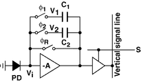
改良点は、図1のセンサのスイッチで表現している部分をMOSトランジスタで構成する場合に生じる問題点を解決するものである。
φRで制御されるMOSトランジスタはキャパシタC1,C2及びフォトダイオード(PD)にたまった電荷を初期化するためのものである。
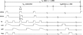
このようにして、φ0で制御されるスイッチをオフするタイミングによって、φ0が"1"である期間に入射した光による電荷はC1に、φ0が"0"である期間に入射した光による電荷はC2に取り込まれることになり、光飛行時間測定法(TOF法)による距離画像計測に必要な動作が行える。
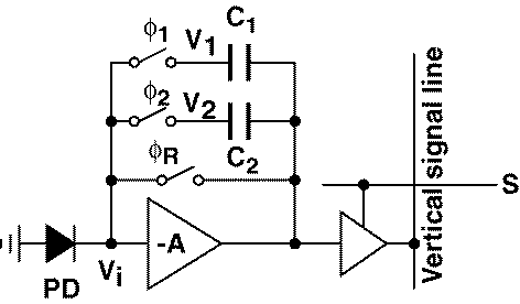
以上は、φ1,φ2で制御されるスイッチにランプ状の電圧を加える例を示したが、その代わりに、φ1,φ2に加える制御パルスの電圧振幅を小さくして、電荷のインジェクション量を減らす方法なども考えられる。この場合、もしφ0で制御されるスイッチがなければ、スイッチのオン抵抗が高くなり、光パルスに対する応答性が悪くなり、距離分解能に影響を与えるが、φ0によって制御されるスイッチにより光パルスに対して高速に応答させることができる。
このソース側つまり、アンプの入力部側に入った電荷は、次にC2を接続したときに、C2に取り込まれる。これは、C2を接続した状態から切り離し、次にC1を接続したときにも同じことが起こる。もし、C1とC2を接続するMOSトランジスタに特性ばらつき(チャネル長、チャネル幅、しきい値電圧)がなければ、注入される電荷の量は同じであるため、影響が相殺される。しかし、特性ばらつきがあると、C1側とC2側に取り込まれる電荷量に差が生じ、オフセット電荷となって影響する。このオフセット電荷は、ランプ波形を用いてφ1,φ2を制御するスイッチをオフすることで、弱反転領域からの小さい電荷に対するばらつきとすることができるため、大きな低減効果が得られる。
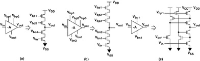
なお、反転増幅器としては、図5に示すような回路が考えられる。図5(a)は、1段のカスコード接続を用いたソース接地カスコード増幅回路、図5(b)は、2段のカスコード接続を用いたソース接地カスコード増幅回路、図5(c)は、ソース接地アンプを用いてゲインを高くしたソース接地カスコード増幅回路である。バイアス電圧(Vbp1,Vbp2,Vbp3,Vbn1,Vbn2)には、すべてのトランジスタが定電流領域で動作するような電圧を与える。また、Vssには、基板(バルク)と同じ電圧、または基板よりも高い電圧に設定することも可能である。
2 第2のMOSトランジスタスイッチ
3 第3のMOSトランジスタスイッチ
PD フォトダイオード
AMP 反転増幅器
C1 第1のキャパシタ
C2 第2のキャパシタ
Claims (3)
- 光源からの光を断続的に対象物に投射し、その反射光の遅れ時間から距離を計測する距離センサにおいて、対象物からの反射光を電荷に変換するフォトダイオード(PD)と、該受光素子からの信号電荷が入力される反転増幅器(AMP)と、第1のキャパシタ(C1)および該第1のキャパシタに直列に接続される第1のMOSトランジスタスイッチ(1)からなる第1の直列回路と、第2のキャパシタ(C2)および該第2のキャパシタに直列に接続される第2のMOSトランジスタスイッチ(2)からなる第2の直列回路と、前記フォトダイオード(PD)と前記反転増幅器(AMP)の入力間に設けられる第3のMOSトランジスタスイッチ(3)と、前記第1、第2及び第3のMOSトランジスタスイッチの開閉を制御する制御手段(4)とを備え、前記第1の直列回路を前記反転増幅器(AMP)の出力と入力間に接続し、かつ、前記第2の直列回路を前記反転増幅器(AMP)の出力と入力間に接続して負帰還増幅器を構成し、対象物からの反射光の遅れ時間に依存する信号電荷を前記第1および第2のMOSトランジスタスイッチ(1,2)の開閉により、前記第1のキャパシタ(C1)および前記第2のキャパシタ(C2)に配分することにより、前記第1および第2のキャパシタ(C1,C2)に蓄積された電荷から距離情報を得るとともに、前記第3のMOSトランジスタスイッチ(3)によりオフセット電荷の影響を低減することを特徴とするオフセット低減機能をもつTOF距離センサ。
- 前記制御手段(4)は、前記第1及び第2のMOSトランジスタスイッチ(1,2)のゲートに対し、ランプ波形の制御信号を与えることにより、前記第1及び第2のMOSトランジスタスイッチ(1,2)を徐々にオフさせることで、オフセット電荷の除去を行うことを特徴とするオフセット低減機能をもつTOF距離センサ。
- 前記フォトダイオード(PD),反転増幅器(AMP),第1のキャパシタ(C1),第1のMOSトランジスタスイッチ(1),第2のキャパシタ(C2),第2のMOSトランジスタスイッチ(2)及び第3のMOSトランジスタスイッチ(3)からなる単位回路を1次元または2次元に配置してなり、画像情報を取得することを特徴とする請求項1または請求項2記載のオフセット低減機能をもつTOF距離センサ。
Priority Applications (1)
| Application Number | Priority Date | Filing Date | Title |
|---|---|---|---|
| JP2004108817A JP4238322B2 (ja) | 2004-04-01 | 2004-04-01 | オフセット低減機能をもつtof距離センサ |
Applications Claiming Priority (1)
| Application Number | Priority Date | Filing Date | Title |
|---|---|---|---|
| JP2004108817A JP4238322B2 (ja) | 2004-04-01 | 2004-04-01 | オフセット低減機能をもつtof距離センサ |
Publications (2)
| Publication Number | Publication Date |
|---|---|
| JP2005291985A true JP2005291985A (ja) | 2005-10-20 |
| JP4238322B2 JP4238322B2 (ja) | 2009-03-18 |
Family
ID=35325069
Family Applications (1)
| Application Number | Title | Priority Date | Filing Date |
|---|---|---|---|
| JP2004108817A Expired - Lifetime JP4238322B2 (ja) | 2004-04-01 | 2004-04-01 | オフセット低減機能をもつtof距離センサ |
Country Status (1)
| Country | Link |
|---|---|
| JP (1) | JP4238322B2 (ja) |
Cited By (12)
| Publication number | Priority date | Publication date | Assignee | Title |
|---|---|---|---|---|
| JP2008089346A (ja) * | 2006-09-29 | 2008-04-17 | Brainvision Inc | 固体撮像素子 |
| WO2009025370A1 (ja) * | 2007-08-22 | 2009-02-26 | Hamamatsu Photonics K.K. | 測距装置 |
| WO2009025369A1 (ja) * | 2007-08-22 | 2009-02-26 | Hamamatsu Photonics K.K. | 測距装置 |
| JP2009047475A (ja) * | 2007-08-15 | 2009-03-05 | Hamamatsu Photonics Kk | 固体撮像素子 |
| JP2012083289A (ja) * | 2010-10-14 | 2012-04-26 | Toyota Motor Corp | 距離計測装置、距離計測方法、及びプログラム |
| JP5110520B2 (ja) * | 2005-08-30 | 2012-12-26 | 国立大学法人静岡大学 | 半導体測距素子及び固体撮像装置 |
| JP5110519B2 (ja) * | 2005-08-30 | 2012-12-26 | 国立大学法人静岡大学 | 半導体測距素子及び固体撮像装置 |
| KR101502122B1 (ko) * | 2013-09-27 | 2015-03-13 | 주식회사 비욘드아이즈 | 깊이 정보를 생성하는 이미지 센서 |
| US9171985B2 (en) | 2012-11-02 | 2015-10-27 | Stmicroelectronics (Research & Development) Limited | Pixel circuit with controlled capacitor discharge time of flight measurement |
| CN109817655A (zh) * | 2018-11-14 | 2019-05-28 | 深圳市光微科技有限公司 | 具有双电荷存储结构的像素单元、图像传感器芯片、成像系统、形成方法和测量深度方法 |
| CN111968998A (zh) * | 2014-12-26 | 2020-11-20 | 松下知识产权经营株式会社 | 摄像装置 |
| CN112835058A (zh) * | 2019-11-05 | 2021-05-25 | 原相科技股份有限公司 | 飞时测距三维传感器及其控制方法 |
Families Citing this family (1)
| Publication number | Priority date | Publication date | Assignee | Title |
|---|---|---|---|---|
| US10324033B2 (en) | 2012-07-20 | 2019-06-18 | Samsung Electronics Co., Ltd. | Image processing apparatus and method for correcting an error in depth |
-
2004
- 2004-04-01 JP JP2004108817A patent/JP4238322B2/ja not_active Expired - Lifetime
Cited By (16)
| Publication number | Priority date | Publication date | Assignee | Title |
|---|---|---|---|---|
| JP5110519B2 (ja) * | 2005-08-30 | 2012-12-26 | 国立大学法人静岡大学 | 半導体測距素子及び固体撮像装置 |
| JP5110520B2 (ja) * | 2005-08-30 | 2012-12-26 | 国立大学法人静岡大学 | 半導体測距素子及び固体撮像装置 |
| JP2008089346A (ja) * | 2006-09-29 | 2008-04-17 | Brainvision Inc | 固体撮像素子 |
| JP2009047475A (ja) * | 2007-08-15 | 2009-03-05 | Hamamatsu Photonics Kk | 固体撮像素子 |
| JP2009047659A (ja) * | 2007-08-22 | 2009-03-05 | Hamamatsu Photonics Kk | 測距装置 |
| JP2009047660A (ja) * | 2007-08-22 | 2009-03-05 | Hamamatsu Photonics Kk | 測距装置 |
| WO2009025369A1 (ja) * | 2007-08-22 | 2009-02-26 | Hamamatsu Photonics K.K. | 測距装置 |
| WO2009025370A1 (ja) * | 2007-08-22 | 2009-02-26 | Hamamatsu Photonics K.K. | 測距装置 |
| JP2012083289A (ja) * | 2010-10-14 | 2012-04-26 | Toyota Motor Corp | 距離計測装置、距離計測方法、及びプログラム |
| US9171985B2 (en) | 2012-11-02 | 2015-10-27 | Stmicroelectronics (Research & Development) Limited | Pixel circuit with controlled capacitor discharge time of flight measurement |
| KR101502122B1 (ko) * | 2013-09-27 | 2015-03-13 | 주식회사 비욘드아이즈 | 깊이 정보를 생성하는 이미지 센서 |
| WO2015046735A1 (ko) * | 2013-09-27 | 2015-04-02 | 주식회사 비욘드아이즈 | 깊이 정보를 생성하는 이미지 센서 |
| CN111968998A (zh) * | 2014-12-26 | 2020-11-20 | 松下知识产权经营株式会社 | 摄像装置 |
| CN109817655A (zh) * | 2018-11-14 | 2019-05-28 | 深圳市光微科技有限公司 | 具有双电荷存储结构的像素单元、图像传感器芯片、成像系统、形成方法和测量深度方法 |
| CN109817655B (zh) * | 2018-11-14 | 2024-12-17 | 光微信息科技(合肥)有限公司 | 具有双电荷存储结构的像素单元、图像传感器芯片和成像系统 |
| CN112835058A (zh) * | 2019-11-05 | 2021-05-25 | 原相科技股份有限公司 | 飞时测距三维传感器及其控制方法 |
Also Published As
| Publication number | Publication date |
|---|---|
| JP4238322B2 (ja) | 2009-03-18 |
Similar Documents
| Publication | Publication Date | Title |
|---|---|---|
| US11917316B2 (en) | Image sensor including pixel circuits | |
| JP4235729B2 (ja) | 距離画像センサ | |
| US8792087B2 (en) | Concept for optical distance measurement | |
| JP4238322B2 (ja) | オフセット低減機能をもつtof距離センサ | |
| US7286174B1 (en) | Dual storage node pixel for CMOS sensor | |
| US10690755B2 (en) | Solid-state imaging device having increased distance measurement accuracy and increased distance measurement range | |
| KR101508410B1 (ko) | 거리 화상 센서, 및 촬상 신호를 비행시간법에 의해 생성하는 방법 | |
| JP7463671B2 (ja) | 距離画像撮像装置、及び距離画像撮像方法 | |
| JP4280822B2 (ja) | 光飛行時間型距離センサ | |
| US7538307B1 (en) | Charge multiplication CMOS image sensor and method for charge multiplication | |
| US20100308209A1 (en) | System for Charge-Domain Electron Subtraction in Demodulation Pixels and Method Therefor | |
| KR102910946B1 (ko) | 광전변환장치, 광전변환 시스템 | |
| EP3499872A1 (en) | Pixel structure, image sensor device and system with pixel structure, and method of operating the pixel structure | |
| US10444364B2 (en) | Pinned photodiode pixels including current mirror-based background light suppression, and imaging devices including the same | |
| US11184567B2 (en) | Imaging device and solid-state imaging element and imaging method used therein | |
| US10276628B2 (en) | Time-of-fight pixel including in-pixel buried channel transistors | |
| CN109073735B (zh) | 距离传感器 | |
| JP2023005963A (ja) | 固体撮像素子、電子機器、および、固体撮像素子の制御方法 | |
| JP2004266597A (ja) | 全画素同時電子シャッタ機能つきイメージセンサ | |
| JPS6337996B2 (ja) | ||
| US11696048B1 (en) | Pixel arrangement and method for operating a pixel arrangement | |
| Kuo et al. | A Half-Pulse 2-Tap Indirect Time-of-Flight Ranging Method with Sub-Frame Operation for Depth Precision Enhancement and Motion Artifact Suppression | |
| CN118696547A (zh) | 成像装置 | |
| JPH05284428A (ja) | 固体撮像装置 | |
| CN112866590A (zh) | 一种减小图像传感器时序电路误差值的方法 |
Legal Events
| Date | Code | Title | Description |
|---|---|---|---|
| A621 | Written request for application examination |
Free format text: JAPANESE INTERMEDIATE CODE: A621 Effective date: 20070223 |
|
| RD03 | Notification of appointment of power of attorney |
Free format text: JAPANESE INTERMEDIATE CODE: A7423 Effective date: 20070223 |
|
| RD05 | Notification of revocation of power of attorney |
Free format text: JAPANESE INTERMEDIATE CODE: A7425 Effective date: 20070223 |
|
| A131 | Notification of reasons for refusal |
Free format text: JAPANESE INTERMEDIATE CODE: A131 Effective date: 20080311 |
|
| A521 | Request for written amendment filed |
Free format text: JAPANESE INTERMEDIATE CODE: A523 Effective date: 20080512 |
|
| A02 | Decision of refusal |
Free format text: JAPANESE INTERMEDIATE CODE: A02 Effective date: 20080624 |
|
| A521 | Request for written amendment filed |
Free format text: JAPANESE INTERMEDIATE CODE: A523 Effective date: 20080723 |
|
| A521 | Request for written amendment filed |
Free format text: JAPANESE INTERMEDIATE CODE: A523 Effective date: 20081008 |
|
| A911 | Transfer to examiner for re-examination before appeal (zenchi) |
Free format text: JAPANESE INTERMEDIATE CODE: A911 Effective date: 20081014 |
|
| TRDD | Decision of grant or rejection written | ||
| A01 | Written decision to grant a patent or to grant a registration (utility model) |
Free format text: JAPANESE INTERMEDIATE CODE: A01 Effective date: 20081125 |
|
| A01 | Written decision to grant a patent or to grant a registration (utility model) |
Free format text: JAPANESE INTERMEDIATE CODE: A01 |
|
| A61 | First payment of annual fees (during grant procedure) |
Free format text: JAPANESE INTERMEDIATE CODE: A61 Effective date: 20081128 |
|
| R150 | Certificate of patent or registration of utility model |
Ref document number: 4238322 Country of ref document: JP Free format text: JAPANESE INTERMEDIATE CODE: R150 Free format text: JAPANESE INTERMEDIATE CODE: R150 |
|
| EXPY | Cancellation because of completion of term |