JP2005251273A - 半導体記憶装置 - Google Patents
半導体記憶装置 Download PDFInfo
- Publication number
- JP2005251273A JP2005251273A JP2004059414A JP2004059414A JP2005251273A JP 2005251273 A JP2005251273 A JP 2005251273A JP 2004059414 A JP2004059414 A JP 2004059414A JP 2004059414 A JP2004059414 A JP 2004059414A JP 2005251273 A JP2005251273 A JP 2005251273A
- Authority
- JP
- Japan
- Prior art keywords
- word line
- bit line
- current selection
- memory cell
- line current
- Prior art date
- Legal status (The legal status is an assumption and is not a legal conclusion. Google has not performed a legal analysis and makes no representation as to the accuracy of the status listed.)
- Pending
Links
- 239000004065 semiconductor Substances 0.000 title claims abstract description 23
- 239000010409 thin film Substances 0.000 claims description 6
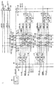
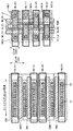
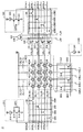
- 238000010586 diagram Methods 0.000 description 20
- 230000004044 response Effects 0.000 description 7
- 230000000052 comparative effect Effects 0.000 description 4
- 238000000034 method Methods 0.000 description 4
- 230000004913 activation Effects 0.000 description 2
- 230000000295 complement effect Effects 0.000 description 2
- 238000013500 data storage Methods 0.000 description 2
- 239000000696 magnetic material Substances 0.000 description 2
- 230000005415 magnetization Effects 0.000 description 2
- 230000003111 delayed effect Effects 0.000 description 1
- 238000012986 modification Methods 0.000 description 1
- 230000004048 modification Effects 0.000 description 1
- 230000005641 tunneling Effects 0.000 description 1
Images


Landscapes
- Mram Or Spin Memory Techniques (AREA)
- Semiconductor Memories (AREA)
- Hall/Mr Elements (AREA)
Priority Applications (1)
| Application Number | Priority Date | Filing Date | Title |
|---|---|---|---|
| JP2004059414A JP2005251273A (ja) | 2004-03-03 | 2004-03-03 | 半導体記憶装置 |
Applications Claiming Priority (1)
| Application Number | Priority Date | Filing Date | Title |
|---|---|---|---|
| JP2004059414A JP2005251273A (ja) | 2004-03-03 | 2004-03-03 | 半導体記憶装置 |
Publications (2)
| Publication Number | Publication Date |
|---|---|
| JP2005251273A true JP2005251273A (ja) | 2005-09-15 |
| JP2005251273A5 JP2005251273A5 (enExample) | 2007-04-05 |
Family
ID=35031602
Family Applications (1)
| Application Number | Title | Priority Date | Filing Date |
|---|---|---|---|
| JP2004059414A Pending JP2005251273A (ja) | 2004-03-03 | 2004-03-03 | 半導体記憶装置 |
Country Status (1)
| Country | Link |
|---|---|
| JP (1) | JP2005251273A (enExample) |
Cited By (2)
| Publication number | Priority date | Publication date | Assignee | Title |
|---|---|---|---|---|
| WO2013187044A1 (ja) | 2012-06-12 | 2013-12-19 | パナソニック株式会社 | 洗濯機システム |
| CN108257635A (zh) * | 2016-12-28 | 2018-07-06 | 上海磁宇信息科技有限公司 | 一种磁性随机存储器及其读取方法 |
Citations (3)
| Publication number | Priority date | Publication date | Assignee | Title |
|---|---|---|---|---|
| JPH087568A (ja) * | 1994-06-27 | 1996-01-12 | Nec Corp | ダイナミックram |
| JP2002170377A (ja) * | 2000-09-22 | 2002-06-14 | Mitsubishi Electric Corp | 薄膜磁性体記憶装置 |
| JP2003203474A (ja) * | 2001-10-26 | 2003-07-18 | Mitsubishi Electric Corp | 薄膜磁性体記憶装置 |
-
2004
- 2004-03-03 JP JP2004059414A patent/JP2005251273A/ja active Pending
Patent Citations (3)
| Publication number | Priority date | Publication date | Assignee | Title |
|---|---|---|---|---|
| JPH087568A (ja) * | 1994-06-27 | 1996-01-12 | Nec Corp | ダイナミックram |
| JP2002170377A (ja) * | 2000-09-22 | 2002-06-14 | Mitsubishi Electric Corp | 薄膜磁性体記憶装置 |
| JP2003203474A (ja) * | 2001-10-26 | 2003-07-18 | Mitsubishi Electric Corp | 薄膜磁性体記憶装置 |
Cited By (3)
| Publication number | Priority date | Publication date | Assignee | Title |
|---|---|---|---|---|
| WO2013187044A1 (ja) | 2012-06-12 | 2013-12-19 | パナソニック株式会社 | 洗濯機システム |
| CN108257635A (zh) * | 2016-12-28 | 2018-07-06 | 上海磁宇信息科技有限公司 | 一种磁性随机存储器及其读取方法 |
| CN108257635B (zh) * | 2016-12-28 | 2020-11-10 | 上海磁宇信息科技有限公司 | 一种磁性随机存储器及其读取方法 |
Similar Documents
| Publication | Publication Date | Title |
|---|---|---|
| US6894922B1 (en) | Memory device capable of performing high speed reading while realizing redundancy replacement | |
| US8625339B2 (en) | Multi-cell per memory-bit circuit and method | |
| KR100505769B1 (ko) | 데이터 판독 참조용 더미셀을 구비한 박막 자성체 기억 장치 | |
| JP5164027B2 (ja) | 半導体記憶装置 | |
| JP5190499B2 (ja) | 半導体記憶装置 | |
| US9728239B2 (en) | Semiconductor memory device | |
| JP4637388B2 (ja) | 薄膜磁性体記憶装置 | |
| JP2013504835A (ja) | スピン移動トルクランダムアクセスメモリのための階層状データ経路を提供する方法およびシステム | |
| JP4274790B2 (ja) | 磁気記憶装置 | |
| JP2010040123A (ja) | 半導体装置 | |
| KR100560133B1 (ko) | 박막자성체 기억장치 | |
| JP2004086934A (ja) | 不揮発性記憶装置 | |
| JP2013196717A (ja) | 半導体記憶装置およびその駆動方法 | |
| US20150269995A1 (en) | Semiconductor device | |
| JP2016167333A (ja) | 疑似ページモードのメモリアーキテクチャおよび方法 | |
| JP2003162898A (ja) | 薄膜磁性体記憶装置 | |
| JP2008147437A (ja) | 磁気抵抗性記憶装置 | |
| JP2005251273A (ja) | 半導体記憶装置 | |
| CN112927737B (zh) | 使用磁性隧道结的非易失寄存器 | |
| US20170047103A1 (en) | Semiconductor storage device | |
| JP5331998B2 (ja) | 不揮発性半導体記憶装置 | |
| JP2010027202A (ja) | 磁性体記憶装置 | |
| WO2011055420A1 (ja) | 半導体装置 | |
| JP2005063553A (ja) | 磁性体記憶装置 | |
| JP2001344969A (ja) | 半導体記憶装置 |
Legal Events
| Date | Code | Title | Description |
|---|---|---|---|
| A521 | Request for written amendment filed |
Free format text: JAPANESE INTERMEDIATE CODE: A523 Effective date: 20070220 |
|
| A621 | Written request for application examination |
Free format text: JAPANESE INTERMEDIATE CODE: A621 Effective date: 20070220 |
|
| A131 | Notification of reasons for refusal |
Free format text: JAPANESE INTERMEDIATE CODE: A131 Effective date: 20091117 |
|
| A02 | Decision of refusal |
Free format text: JAPANESE INTERMEDIATE CODE: A02 Effective date: 20100316 |