JP2005197859A - High frequency power amplifier circuit - Google Patents
High frequency power amplifier circuit Download PDFInfo
- Publication number
- JP2005197859A JP2005197859A JP2004000169A JP2004000169A JP2005197859A JP 2005197859 A JP2005197859 A JP 2005197859A JP 2004000169 A JP2004000169 A JP 2004000169A JP 2004000169 A JP2004000169 A JP 2004000169A JP 2005197859 A JP2005197859 A JP 2005197859A
- Authority
- JP
- Japan
- Prior art keywords
- current
- voltage
- transistor
- bias
- power amplifier
- Prior art date
- Legal status (The legal status is an assumption and is not a legal conclusion. Google has not performed a legal analysis and makes no representation as to the accuracy of the status listed.)
- Pending
Links
Images


Landscapes
- Transmitters (AREA)
- Control Of Amplification And Gain Control (AREA)
- Amplifiers (AREA)
Abstract
Description
本発明は、高周波信号を増幅して出力する高周波電力増幅回路さらには増幅用トランジスタのしきい値電圧の製造ばらつきに伴うアイドル電流の変動を低減するのに適用して有効な技術に関し、例えば携帯電話機に使用される高周波電力増幅回路およびそれを組み込んだ電子部品(パワーモジュール)に利用して有効な技術に関する。 The present invention relates to a high-frequency power amplifier circuit that amplifies and outputs a high-frequency signal, and also to a technique that is effective when applied to reduce fluctuations in idle current due to manufacturing variations in threshold voltage of an amplifying transistor. The present invention relates to a high-frequency power amplifier circuit used for a telephone and a technology effective for use in an electronic component (power module) incorporating the high-frequency power amplifier circuit.
一般に、携帯電話機等の無線通信装置(移動体通信装置)における送信側出力部には、変調後の送信信号を増幅する高周波電力増幅回路(パワーアンプ)が設けられている。従来の無線通信装置においては、ベースバンド回路もしくはマイクロプロセッサ等の制御回路からの送信要求レベルに応じて高周波電力増幅回路の増幅率を制御するため、高周波電力増幅回路もしくはアンテナの出力電力を検出して検出信号とベースバンドLSIからの送信要求レベルに基づいて送信出力の制御信号を生成するAPC(Automatic Power Control)回路と呼ばれる回路から出力される制御電圧によって通話に必要な出力電力となるように、高周波電力増幅回路のバイアス電圧を制御する構成が採用されている(例えば、特許文献1参照)。また、高周波電力増幅回路の増幅素子には、MOSトランジスタやバイポーラ・トランジスタ、GaAsMESFETなど各種化合物半導体トランジスタが使用されているが、近年においてはMOSトランジスタが比較的多く採用されるようになっている。 In general, a transmission-side output unit in a wireless communication device (mobile communication device) such as a mobile phone is provided with a high-frequency power amplification circuit (power amplifier) that amplifies a modulated transmission signal. In conventional wireless communication devices, the output power of a high-frequency power amplifier circuit or antenna is detected in order to control the amplification factor of the high-frequency power amplifier circuit according to the transmission request level from a control circuit such as a baseband circuit or a microprocessor. Thus, output power required for a call is obtained by a control voltage output from a circuit called an APC (Automatic Power Control) circuit that generates a transmission output control signal based on a detection signal and a transmission request level from the baseband LSI. A configuration for controlling the bias voltage of the high-frequency power amplifier circuit is employed (see, for example, Patent Document 1). In addition, various compound semiconductor transistors such as MOS transistors, bipolar transistors, and GaAs MESFETs are used as the amplifying elements of the high-frequency power amplifier circuit. In recent years, relatively many MOS transistors have been adopted.
ところで、従来、携帯電話機における通信方式の一つにGSM(Global System for Mobile Communication)と呼ばれる方式がある。このGSM方式は、変調方式に搬送波の位相を送信データに応じてシフトするGMSK(Gaussian Minimum Shift Keying )と呼ばれる位相変調方式が用いられている。GSM方式の通信システムでは位相変調された信号を要求出力レベルに応じて増幅して出力すれば良い。そこで、このGSM方式の携帯電話機においては、一般に、入力信号の振幅を固定してバイアス制御回路で高周波電力増幅回路の各増幅素子のアイドル電流を要求出力レベルに応じて制御して出力電力を制御することが行なわれている。 By the way, conventionally, there is a system called GSM (Global System for Mobile Communication) as one of communication systems in a mobile phone. In this GSM system, a phase modulation system called GMSK (Gaussian Minimum Shift Keying) that shifts the phase of a carrier wave according to transmission data is used as a modulation system. In a GSM communication system, a phase-modulated signal may be amplified and output according to a required output level. Therefore, in this GSM cellular phone, generally, the amplitude of the input signal is fixed, and the bias control circuit controls the idle current of each amplifying element of the high frequency power amplifier circuit according to the required output level to control the output power. To be done.
一方、位相変調と振幅変調を伴う8PSK変調方式を採用するEDGE方式の通信システムやW−CDMA方式の携帯電話機では、ベースバンド回路から供給される制御電流(もしくは制御電流)に応じてパワーアンプのバイアス電流(もしくはバイアス電圧)を固定した状態で入力信号の振幅を送信要求レベルに基づいて変化させて出力電力を制御する方法が提案されている。
上記従来の高周波電力増幅回路のバイアス制御方式においては、増幅素子に流されるアイドル電流はバイアス制御回路からのバイアス電圧もしくはバイアス電流によって一義的に決まるようになっている。ところが、増幅素子としてMOSトランジスタを使用した高周波電力増幅回路においては、MOSトランジスタのしきい値電圧が製造ばらつきで所望の値からずれることがあり、それによって例えバイアス電圧が一定でも増幅用トランジスタに流れるアイドル電流が変化してしまい所望の出力電力が得られないという課題がある。 In the conventional bias control system of the high frequency power amplifier circuit, the idle current flowing through the amplifier element is uniquely determined by the bias voltage or bias current from the bias control circuit. However, in a high-frequency power amplifier circuit using a MOS transistor as an amplifying element, the threshold voltage of the MOS transistor may deviate from a desired value due to manufacturing variations, so that even if the bias voltage is constant, it flows to the amplifying transistor. There is a problem that the desired output power cannot be obtained because the idle current changes.
従来、かかるMOSトランジスタのしきい値電圧の製造ばらつきによるアイドル電流の変化を防止するため、増幅素子にバイアスを与えるバイアス制御回路内にばらつき調整のラダー抵抗を設けておいて、製造後にMOSトランジスタのしきい値電圧を測定してそのばらつきに応じてラダー抵抗の抵抗比を変化させることで生成されるバイアス電圧もしくはバイアス電流を調整して増幅用トランジスタに流れるアイドル電流を一定にするようにした技術がある。 Conventionally, in order to prevent a change in idle current due to manufacturing variations in threshold voltage of such a MOS transistor, a variation adjusting ladder resistor is provided in a bias control circuit for applying a bias to the amplifying element. A technology that adjusts the bias voltage or bias current generated by measuring the threshold voltage and changing the resistance ratio of the ladder resistor according to the variation to make the idle current flowing through the amplifying transistor constant. There is.
また、ラダー抵抗の抵抗比を変更する方法としては、レーザーを用いて接続箇所を切断する方法やワイヤボンディングで抵抗ノード間を短絡する方法が一般的であるが、これらの方法は製造設備およびプロセスが複雑になるとともにバイアス制御回路が形成された半導体チップのサイズが大きくなるという不具合がある。なお、ラダー抵抗の抵抗ノード間を短絡する方法として、ワイヤボンディングの代わりに、ボンディングパッドを近接して配置しておいてパッド間に跨るようにボンディングボールを形成することで短絡を行なう方法も考えられる。この方法は、ワイヤボンディング方式よりも効率的でありチップサイズも低減できるという利点があるが、製造設備およびプロセスの簡略化の点では十分なものではない。 In addition, as a method of changing the resistance ratio of the ladder resistor, a method of cutting a connection portion using a laser or a method of short-circuiting between resistance nodes by wire bonding is generally used. And the size of the semiconductor chip on which the bias control circuit is formed increases. As a method of short-circuiting between the resistance nodes of the ladder resistor, a method of short-circuiting by forming bonding balls so as to straddle between pads instead of wire bonding is also considered. It is done. Although this method is more efficient than the wire bonding method and has the advantage that the chip size can be reduced, it is not sufficient in terms of simplification of manufacturing equipment and processes.
この発明の目的は、電力増幅用トランジスタのバイアス電圧を変化させて出力電力を制御する無線通信システムにおいて、電力増幅用MOSトランジスタのしきい値電圧が製造ばらつきで所定の値からずれたとしても所望の大きさのアイドル電流を流すことができ、それによって安定した出力電力が得られるバイアス制御回路を内蔵した高周波電力増幅回路およびそれを用いた高周波電力増幅用電子部品を提供することにある。 An object of the present invention is to provide a wireless communication system that controls output power by changing a bias voltage of a power amplification transistor, even if the threshold voltage of the power amplification MOS transistor deviates from a predetermined value due to manufacturing variations. It is an object of the present invention to provide a high-frequency power amplifier circuit incorporating a bias control circuit that can flow an idle current having a magnitude of 1 to obtain a stable output power, and an electronic component for high-frequency power amplification using the same.
この発明の他の目的は、電力増幅用トランジスタのバイアス電圧を変化させて出力電力を制御する無線通信システムにおいて、電力増幅用トランジスタのアイドル電流のばらつきを補正するためのレーザトリミングやワイヤボンディング、ボールボンディングなどの工程を不要にして、製造設備および製造プロセスの簡略化を図ることができるバイアス制御回路を内蔵した高周波電力増幅回路およびそれを用いた高周波電力増幅用電子部品を提供することにある。 Another object of the present invention is to provide laser trimming, wire bonding, and ball for correcting variations in idle current of a power amplification transistor in a wireless communication system that controls output power by changing a bias voltage of the power amplification transistor. An object of the present invention is to provide a high-frequency power amplifier circuit incorporating a bias control circuit that can simplify the manufacturing equipment and the manufacturing process without using a step such as bonding, and an electronic component for high-frequency power amplification using the same.
この発明の前記ならびにそのほかの目的と新規な特徴については、本明細書の記述および添付図面から明らかになるであろう。 The above and other objects and novel features of the present invention will be apparent from the description of this specification and the accompanying drawings.
本願において開示される発明のうち代表的なものの概要を説明すれば、下記のとおりである。
すなわち、電力増幅用MOSトランジスタにバイアス制御電圧に応じてバイアス電圧を与え所望のアイドル電流を流して出力電力を制御するようにした高周波電力増幅回路において、バイアス制御回路に電力増幅用MOSトランジスタと同一構造のトランジスタを設け、該トランジスタの制御端子に定電圧を印加してしきい値電圧に応じた電流が流れるようにしておいて、該電流をしきい値電圧ばらつき補償電流として用いて、電力増幅用MOSトランジスタに与えるバイアス電圧を自動調整できるようにバイアス制御回路を構成した。
Outlines of representative ones of the inventions disclosed in the present application will be described as follows.
That is, in a high frequency power amplifier circuit in which a bias voltage is applied to a power amplification MOS transistor according to a bias control voltage and a desired idle current is supplied to control output power, the bias control circuit is the same as the power amplification MOS transistor. A transistor having a structure is provided, a constant voltage is applied to the control terminal of the transistor so that a current corresponding to the threshold voltage flows, and the current is used as a threshold voltage variation compensating current to amplify power. The bias control circuit is configured so that the bias voltage applied to the MOS transistor can be automatically adjusted.
かかる特性のバイアス制御回路は、例えばバイアス制御電圧に比例した基準電流を生成する基準電流生成回路と、電力増幅用トランジスタと同一構造のダミートランジスタを備えそのしきい値電圧に応じた電流を生成するしきい値電圧ばらつき補償電流生成回路とを設け、上記基準電流と補償電流とを合成した電流を電圧に変換して電力増幅用MOSトランジスタに印加するように構成することで得られる。なお、上記ダミートランジスタは、電力増幅用トランジスタと構造は同一であってもサイズは小さなものとする。 The bias control circuit having such characteristics includes, for example, a reference current generation circuit that generates a reference current proportional to the bias control voltage, and a dummy transistor having the same structure as the power amplification transistor, and generates a current corresponding to the threshold voltage. A threshold voltage variation compensation current generation circuit is provided, and a current obtained by combining the reference current and the compensation current is converted into a voltage and applied to the power amplification MOS transistor. The dummy transistor is small in size even if it has the same structure as the power amplification transistor.
上記した手段によれば、電力増幅用MOSトランジスタのしきい値電圧が製造ばらつきを有するとダミートランジスタの電流のしきい値電圧も同じようにばらついて、しきい値電圧のばらつきに応じた電流がダミートランジスタに流れるため、この電流を基準電流と合成して電圧に変換して電力増幅用MOSトランジスタに印加することで、電力増幅用トランジスタにしきい値電圧のばらつきの影響を受けないアイドル電流を流すことができるようになる。また、しきい値電圧がばらついても回路によってアイドル電流が一定に維持されるようにされるため、ラダー抵抗を用いたトリミング回路を設ける必要がなく、回路規模が小さくなるとともに、レーザトリミングやワイヤボンディング、ボールボンディングなどの工程が不要となる。 According to the above means, if the threshold voltage of the power amplifying MOS transistor has a manufacturing variation, the threshold voltage of the current of the dummy transistor varies in the same manner, and a current corresponding to the variation of the threshold voltage is obtained. Since the current flows through the dummy transistor, this current is combined with the reference current, converted into a voltage, and applied to the power amplification MOS transistor, thereby flowing an idle current that is not affected by variations in threshold voltage to the power amplification transistor. Will be able to. In addition, since the idle current is maintained constant by the circuit even if the threshold voltage varies, it is not necessary to provide a trimming circuit using a ladder resistor, the circuit scale is reduced, and laser trimming and wire are reduced. Steps such as bonding and ball bonding are not required.
本願において開示される発明のうち代表的なものによって得られる効果を簡単に説明すれば下記のとおりである。
すなわち、本発明に従うと、電力増幅用トランジスタのバイアス電圧を変化させて出力電力を制御する無線通信システムにおいて、電力増幅用MOSトランジスタのしきい値電圧が製造ばらつきで所定の値からずれたとしても所望の大きさのアイドル電流を流すことができ、それによって安定した出力電力が得られるようになる。また、電力増幅用トランジスタのアイドル電流のばらつきを補正するためのレーザトリミングやワイヤボンディング、ボールボンディングなどの工程が不要となるため、製造設備および製造プロセスが簡略化され製造所要時間の短縮、製造コストの低減が達成されるという効果がある。
The effects obtained by the representative ones of the inventions disclosed in the present application will be briefly described as follows.
That is, according to the present invention, in the wireless communication system that controls the output power by changing the bias voltage of the power amplification transistor, even if the threshold voltage of the power amplification MOS transistor deviates from a predetermined value due to manufacturing variations. An idle current having a desired magnitude can be flowed, whereby stable output power can be obtained. In addition, laser trimming, wire bonding, ball bonding, and other processes for correcting variations in idle current of power amplification transistors are not required, simplifying manufacturing equipment and manufacturing processes, reducing manufacturing time, and manufacturing costs. There is an effect that reduction of the above is achieved.
以下、本発明の好適な実施例を図面に基づいて説明する。
図1は、本発明を適用した高周波電力増幅器(パワーモジュール200)の実施例を示したものである。本明細書においては、表面や内部にプリント配線が施されたセラミック基板のような絶縁基板に複数の半導体チップとディスクリート部品が実装されて上記プリント配線やボンディングワイヤで各部品が所定の役割を果たすように結合されることであたかも一つの電子部品として扱えるように構成されたものをモジュールと称する。
Preferred embodiments of the present invention will be described below with reference to the drawings.
FIG. 1 shows an embodiment of a high-frequency power amplifier (power module 200) to which the present invention is applied. In this specification, a plurality of semiconductor chips and discrete components are mounted on an insulating substrate such as a ceramic substrate with printed wiring on the surface or inside, and each component plays a predetermined role in the printed wiring or bonding wire. A module that can be handled as one electronic component is called a module.
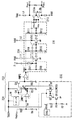
この実施例のパワーモジュール200は、入力高周波信号Pinを増幅する電力増幅用FET(電界効果トランジスタ)を含む高周波電力増幅部210と、該高周波電力増幅部210の出力電力を検出する出力電力検出回路220と、前記高周波電力増幅部210の各段の電力増幅用FETにバイアス電圧を与えて各FETに流すアイドル電流を制御するバイアス制御回路230と、外部のベースバンド部から供給される出力レベル指示信号Vrampと前記出力電力検出回路220からの検出電圧Vdetとを比較してその電位差に応じた制御電圧Vapcを前記バイアス制御回路230へ与える誤差アンプ(APC回路)250とからなる。
The
特に制限されるものでないが、この実施例の高周波電力増幅部210は、3個の電力増幅用FET211、212、213を備え、このうち後段のFET212,213はそれぞれ前段のFET211,212のドレイン端子にゲート端子が接続され、全体で3段の増幅回路として構成されている。また、各段のFET211,212,213のゲート端子には、バイアス制御回路230から供給されるゲートバイアス電圧Vb1,Vb2,Vb3が印加され、これらの電圧に応じたアイドル電流が各FET211,212,213にそれぞれ流されるようにされている。
Although not particularly limited, the high-frequency power amplifying
各段のFET211,212,213のドレイン端子にはそれぞれインダクタL1,L2,L3を介して電源電圧Vddが印加されている。初段のFET211のゲート端子と入力端子INとの間には、インピーダンス整合回路241および直流カットの容量素子C1が設けられ、これらの回路及び素子を介して高周波信号PinがFET211のゲート端子に入力される。
The power supply voltage Vdd is applied to the drain terminals of the
初段のFET211のドレイン端子と2段目のFET212のゲート端子との間には、インピーダンス整合回路242および直流カットの容量素子C2が接続されている。また、2段目のFET212のドレイン端子と最終段のFET213のゲート端子との間には、インピーダンス整合回路243および直流カットの容量素子C3が接続されている。そして、最終段のFET213のドレイン端子がインピーダンス整合回路244および容量素子C4を介して出力端子OUTに接続されており、高周波入力信号Pinの直流成分をカットし交流成分を増幅した信号Poutを出力端子OUTより出力する。
Between the drain terminal of the first-
出力電力検出回路220は、最終段の電力増幅用EFT213のドレイン端子とモジュールの出力端子OUTとの間に設けられたインピーダンス整合回路244の内部ノードに一方の端子が接続された抵抗Riおよび該抵抗と直列に接続された容量Ciにより取り出された交流信号が入力され、この交流信号を半波整流して電圧に変換して検波電圧Vdetとして出力するように構成される。出力電力検出回路220の回路形式としては種々のものが考えられるので、本実施例では具体的な回路の開示は省略する。
The output
本実施例においては、電力増幅用EFT211〜213として、チップ上で横方向に電極を拡散させたいわゆるLDMOS(Laterally Diffused MOSFET)と呼ばれるMOSトランジスタが用いられている。
In this embodiment, MOS transistors called LDMOS (Laterally Diffused MOSFET) in which electrodes are diffused laterally on a chip are used as the
なお、この実施例のパワーモジュール200は、特に制限されるものでないが、破線で囲まれた部分が半導体集積回路化されている。すなわち電力増幅部210の各素子(インダクタL1〜L3およびインピーダンス整合回路244を除く)およびバイアス制御回路230の各素子と、出力電力検出回路220の各素子(抵抗Riおよび容量Ciを除く)、直流成分をカットする容量素子C1,C2,C3が、単結晶シリコンのような1個の半導体チップ上に半導体集積回路IC1として構成されている。そして、この半導体集積回路IC1と、電力増幅部210のインダクタL1〜L3と、出力電力検出回路220の入力用の抵抗Riおよび容量iとが、1つのセラミック基板上に実装されてパワーモジュールとして構成されている。インピーダンス整合回路241〜244を構成するインダクタは、半導体チップのパッド間に接続されたボンディングワイヤあるいはモジュール基板上に形成されたマイクロストリップラインにより形成することができる。
The
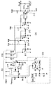
図2は、バイアス制御回路230の具体的な回路例を示す。
この実施例のバイアス制御回路230は、入力されたバイアス制御電圧Vapcに基づいて基準となる電流を生成する基準電流部231と、電力増幅用トランジスタのしきい値電圧Vthのばらつきに応じた電流を生成するVthばらつき補償電流生成部232と、生成された基準電流とVthばらつき補償電流とを合成した電流を電圧に変換する電流−電圧変換部233と、変換された電圧を抵抗分割してバイアス電圧Vb1〜Vb3として各増幅段の増幅用トランジスタ211〜213のゲート端子に印加する抵抗分圧回路234とからなる。増幅用トランジスタ213は、並列接続された2個のMOSトランジスタ213a,213bから構成されている。他の増幅用トランジスタ211,212に比べて大きな電流を流すため、サイズを大きくする必要があるためである。
FIG. 2 shows a specific circuit example of the
The
基準電流部231は、バイアス制御電圧Vapcを抵抗分割する直列抵抗R3,R4と、非反転入力端子に抵抗R3,R4により分割された電圧Vaが印加された差動アンプAMP1と、該差動アンプAMP1の入力電圧Vaの上限を制限するリミッタLIMと、電源電圧Vddと接地点との間に直列に接続されたMOSトランジスタQ4および抵抗R5と、MOSトランジスタQ4と同一のゲート電圧をゲートに受けてQ4のドレイン電流に比例した電流を流すMOSトランジスタQ5と、該トランジスタQ5のドレイン端子と接地点との間に接続された抵抗R6とからなる。なお、トランジスタQ4と抵抗R5は、差動アンプAMP1の出力段とみなすことができる。この実施例の基準電流部231は、トランジスタQ4と抵抗R5との接続ノードの電位V0が差動アンプAMP1の反転入力端子にフィードバックされることにより、V0を差動アンプAMP1の入力電圧Vaに一致させるような基準電流I1がMOSトランジスタQ4に流される。
The reference
Vthばらつき補償電流生成部232は、バンドギャップリファランス回路のような基準電圧回路RVGと、該基準電圧回路RVGにより生成された基準電圧Vrefを抵抗分割する直列抵抗R1,R2と、増幅用トランジスタ211〜213と同一のLDMOSにより構成されたダミートランジスタQ1と、該トランジスタQ1のドレイン端子と電源電圧Vddとの間に接続されたトランジスタQ2と、該トランジスタQ1とゲート共通接続されてカレントミラーを構成するトランジスタQ3とからなる。このトランジスタQ3は、ドレイン端子が上記基準電流部231のトランジスタQ4と抵抗R5との接続ノードに接続されており、トランジスタQ4に流れる電流I1とQ3の電流I2とを合成した電流I1+I2が抵抗R5に流れるようにされている。
The Vth variation compensating
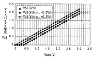
次に、本実施例のバイアス制御回路230の特性と作用を、図3のグラフを用いて説明する。
基準電流部231においては、差動アンプAMP1の作用によりバイアス制御電圧Vapcに応じた電流I1がトランジスタQ4に流されるため、Vthばらつき補償電流生成部232の電流I2を考えなければトランジスタQ4に流れる電流I1はバイアス制御電圧Vapcに比例する。そして、トランジスタQ4とQ5のゲート幅が所定のサイズ比となるように形成されることにより、Q5にはQ4の電流に比例した電流が流され、これが抵抗R6で電圧に変換され、ボルテージフォロワとして動作するアンプAMP2によりインピーダンス変換されて、増幅用トランジスタ211〜213のゲートバイアス電圧Vb1〜Vb3を生成する抵抗分圧回路234に供給される。そのため、電流−電圧変換部233の出力電圧はバイアス制御電圧Vapcに比例した電圧となり、これを抵抗分割して生成される増幅用トランジスタ213のゲートバイアス電圧Vb3は、図3に示すように、バイアス制御電圧Vapcに比例した電圧となる。
Next, the characteristics and operation of the
In the reference
なお、この実施例のバイアス制御回路230においては、基準電流部231の差動アンプAMP1の入力端子にリミッタLIMが接続され、入力信号を制限しているため、図3に破線で示すように、増幅用トランジスタ213のゲートバイアス電圧Vb3はバイアス制御電圧Vapcが例えば3Vを超えると一定の電圧となる。図3には示されていないが、増幅用トランジスタ211,212のゲートバイアス電圧Vb1,Vb2もVb3と傾きは異なるが同様にバイアス制御電圧Vapcに比例した電圧となる。また、図3に●印で示されているように、バイアス制御電圧Vapcが0.2Vよりも高くなるとゲートバイアス電圧Vb3が立ち上がるのは、ダミートランジスタQ1のしきい値電圧Vthにばらつきがない状態で、Vthばらつき補償電流生成部232から基準電流部231の抵抗R5へ少しだけ電流I2が流れるように、抵抗R1,R2の比が設定されているためである。
In the
本実施例のバイアス制御回路230においては、Vthばらつき補償電流生成部232のダミートランジスタQ1が増幅用トランジスタ211〜213と同一のLDMOSにより構成されているため、増幅用トランジスタ211〜213のしきい値電圧VthがばらつくとダミートランジスタQ1のしきい値電圧Vthも同じようにばらつくこととなる。そのため、例えば増幅用トランジスタ211〜213のしきい値電圧Vthが高くなってアイドル電流が減少しようとすると、ダミートランジスタQ1のしきい値電圧Vthも同じように高くなって電流I2が減少する。
In the
そして、差動アンプAMP1は抵抗R5に流れる電流I1+I2を維持するようにMOSトランジスタQ4のゲート電圧を変化させるため、I2が減った分だけQ4の電流I1が増加される。これによって、電流−電圧変換部233の出力電圧が高くなり、増幅用トランジスタ211〜213のゲートバイアス電圧Vb1〜Vb3が高くされてアイドル電流を多く流そうとする。そのため、増幅用トランジスタ211〜213のしきい値電圧Vthの上昇によるアイドル電流の減少分とダミートランジスタQ1のしきい値電圧Vthの上昇によるアイドル電流の増加分とが相殺しあってアイドル電流が一定に保たれる。
Since the differential amplifier AMP1 changes the gate voltage of the MOS transistor Q4 so as to maintain the current I1 + I2 flowing through the resistor R5, the current I1 of Q4 is increased by the amount of decrease of I2. As a result, the output voltage of the current-
増幅用トランジスタ211〜213のしきい値電圧Vthが低い方へばらつくと、増幅用トランジスタ211〜213のアイドル電流が増加しようとするが、ダミートランジスタQ1のしきい値電圧Vthも同じように低くなってゲートバイアス電圧Vb1〜Vb3が低くされてアイドル電流を減少させるように作用するためアイドル電流が一定に保たれる。
When the threshold voltage Vth of the amplifying
なお、上記実施例では、基準電流生成部231とVthばらつき補償電流生成部232で生成した電流を合成して電圧に変換し抵抗分圧回路234で分圧して各増幅段の増幅用MOSトランジスタにゲートバイアス電圧を与えるようにした場合を説明したが、例えば図4に示すように、増幅用トランジスタ211〜213にカレントミラー接続されたMOSトランジスタQ11〜Q13を設け、基準電流生成部231のトランジスタQ5の電流を増幅用MOSトランジスタ211とカレントミラー接続されたMOSトランジスタQ11に、またQ5と並列に設けられ同一のゲート電圧が印加されたトランジスタQ6,Q7の電流を増幅用MOSトランジスタ212,213とカレントミラー接続されたMOSトランジスタQ12,Q13に流していわゆるカレントミラー方式でゲートバイアスを与えるバイアス制御回路に対しても本発明を適用することができる。
In the above embodiment, the currents generated by the reference
図5は、前記実施例のパワーモジュールを適用して有効な無線通信システムの一例として、GSMとDCSの2つの通信方式の無線通信が可能なシステムの概略の構成を示す。
図5において、ANTは信号電波の送受信用アンテナ、100はGSMやDCSのシステムにおけるGMSK変調や復調を行なうことができる変復調回路や送信データ(ベースバンド信号)に基づいてI,Q信号を生成したり受信信号から抽出されたI,Q信号を処理する回路を有する高周波信号処理回路(ベースバンド回路)110や受信信号を増幅するロウノイズアンプLNA1,LNA2等が1つの半導体チップ上に形成されてなる高周波信号処理用半導体集積回路(ベースバンドIC)と送信信号から高調波成分を除去するバンドパスフィルタBPF1,BPF2、受信信号から不要波を除去するバンドパスフィルタBPF3,BPF4などが1つのパッケージに実装されてなる電子デバイス(以下、RFデバイスと称する)である。Tx‐MIX1,Tx-MIX2は各々GSMとDCSの送信信号をアップンコンバートするミキサ、Rx‐MIX1,Rx-MIX2は各々GSMとDCSの受信信号をダウンコンバートするミキサである。
FIG. 5 shows a schematic configuration of a system capable of wireless communication of two communication systems, GSM and DCS, as an example of an effective wireless communication system to which the power module of the embodiment is applied.
In FIG. 5, ANT is an antenna for transmitting and receiving signal radio waves, 100 is a modulation / demodulation circuit capable of performing GMSK modulation and demodulation in GSM and DCS systems, and I and Q signals are generated based on transmission data (baseband signals). A high-frequency signal processing circuit (baseband circuit) 110 having a circuit for processing I and Q signals extracted from received signals, low noise amplifiers LNA1 and LNA2 for amplifying received signals, and the like are formed on one semiconductor chip. A high-frequency signal processing semiconductor integrated circuit (baseband IC), bandpass filters BPF1 and BPF2 for removing harmonic components from a transmission signal, bandpass filters BPF3 and BPF4 for removing unnecessary waves from a reception signal, etc. in one package A mounted electronic device (hereinafter referred to as an RF device) Tx-MIX1 and Tx-MIX2 are mixers that up-convert GSM and DCS transmission signals, respectively, and Rx-MIX1 and Rx-MIX2 are mixers that down-convert GSM and DCS reception signals, respectively.
また、図5において、200はベースバンドIC100から供給される高周波信号を増幅する前記実施例のパワーモジュール、300は送信信号に含まれる高調波などのノイズを除去するフィルタLPF1,LPF2、GSMの信号とDCSの信号を合成したり分離したりする分波器DPX1,DPX2、送受信の切替えスイッチT/R−SWなどを含むフロントエンド・モジュールである。
In FIG. 5,
図5に示されているように、この実施例では、ベースバンドIC110からバイアス制御回路230に対してGSMかDCSかを示すモード選択信号VBANDが供給され、バイアス制御回路230はこの制御信号VBANDに基づいて、モードに応じたバイアス電流を生成しパワーアンプ210aと210bのいずれかに供給する。また、ベースバンドIC110からパワーモジュール200内のAPC回路(誤差アンプ)250へ出力レベル指示信号Vrampが供給され、APC回路(誤差アンプ)250は出力レベル指示信号Vrampと出力電力検出回路220からの検出電圧Vdetとを比較してバイアス制御回路230対する出力制御信号Vapcを生成し、バイアス制御回路230は出力制御信号Vapcに応じてパワーアンプ210a,210bのゲインを制御し、これに応じてパワーアンプ210a,210bの出力電力が変化するように制御される。
As shown in FIG. 5, in this embodiment, a mode selection signal VBAND indicating GSM or DCS is supplied from the
なお、図5には示されていないが、上記デバイスやモジュール以外に、RFデバイス100に対する制御信号やパワー制御信号PCSの基になる出力レベル指示信号を生成してシステム全体を制御するマイクロプロセッサ(CPU)を設けるようにしても良い。
Although not shown in FIG. 5, in addition to the devices and modules described above, a microprocessor (not shown in FIG. 5) that generates an output level instruction signal based on a control signal for the
以上本発明者によってなされた発明を実施例に基づき具体的に説明したが、本発明は上記実施例に限定されるものではなく、その要旨を逸脱しない範囲で種々変更可能であることはいうまでもない。例えば前記実施例の高周波電力増幅回路では、電力増幅素子を3段接続しているが、2段構成としたり、4段以上の構成としても良い。また、実施例では、電力増幅素子211〜213として、LDMOSが使用されているが、通常のCMOSプロセスで形成されるMOSFETやバイポーラ・トランジスタ、GaAsMESFET、ヘテロ接合バイポーラ・トランジスタ(HBT)、HEMT(High Electron Mobility Transistor)等他のトランジスタを用いても良い。ただし、その場合、ダミートランジスタQ1も増幅用トランジスタ211〜213と同一の素子で構成するのが望ましい。
The invention made by the present inventor has been specifically described based on the embodiments. However, the present invention is not limited to the above embodiments, and various modifications can be made without departing from the scope of the invention. Nor. For example, in the high-frequency power amplifier circuit of the above-described embodiment, the power amplifier elements are connected in three stages, but may be configured in two stages or in four or more stages. In the embodiment, LDMOS is used as the
さらに、前記実施例では、ベースバンド部からの出力レベル指示信号Vrampと出力電力検出回路220からの検出電圧Vdetとを比較してバイアス制御回路230へ出力制御電圧Vapcを生成する誤差アンプ(APC回路)250が電力増幅回路210や出力電力検出回路220と同一の半導体チップ上に形成されている場合を説明したが、誤差アンプ(APC回路)250は別個の半導体チップ上に形成されていても良い。
Further, in the above embodiment, an error amplifier (APC circuit) that generates an output control voltage Vapc to the
以上の説明では主として本発明者によってなされた発明をその背景となった利用分野であるGSMとDCSの2つの通信方式による送受信が可能なデュアルモードの無線通信システムを構成するパワーモジュールに適用した場合を説明したが、本発明はそれに限定されるものでなく、他の通信方式や、GSMとDCSとPCS(Personal Communications System)など3以上の通信方式による送受信が可能なマルチモードの携帯電話機や移動電話機などの無線通信システムを構成するパワーモジュールあるいは無線LAN用の高周波電力増幅回路およびパワーモジュールに利用することができる。 In the above description, when the invention made mainly by the present inventor is applied to a power module constituting a dual-mode wireless communication system capable of transmission / reception by two communication systems, GSM and DCS, which are the fields of use behind it. However, the present invention is not limited to this, and a multi-mode mobile phone or mobile device capable of transmission / reception by other communication methods, or three or more communication methods such as GSM, DCS, and PCS (Personal Communications System). It can be used for a power module constituting a wireless communication system such as a telephone or a high frequency power amplifier circuit and a power module for a wireless LAN.
100 RFデバイス
110 ベースバンド回路
200 パワーモジュール
210,210a,210b 高周波電力増幅回路
211,212,213 電力増幅用FET
220 出力電力検出回路
230 バイアス制御回路
231 基準電流生成部
232 Vthばらつき補償電流生成部
233 電流−電圧変換部
234 抵抗分圧回路
241〜244 インピーダンス整合回路
250 誤差アンプ(APC回路)
300 フロントエンド・モジュール
DESCRIPTION OF
220 Output
300 Front-end module
Claims (5)
前記バイアス制御回路は、前記電力増幅用MOSトランジスタと同一構造を有しゲート端子に定電圧が印加されてしきい値電圧に応じた電流が流れるようにされたダミートランジスタを備え、該ダミートランジスタの電流をしきい値電圧ばらつき補償電流として用いて、前記電力増幅用MOSトランジスタのしきい値電圧のばらつきに関わらず該トランジスタに所定のバイアス電流が流れるようなバイアスを与えるように構成されていることを特徴とする高周波電力増幅回路。 A high-frequency power amplifier circuit including a bias control circuit that applies a bias according to a bias control voltage to a power amplification MOS transistor, and controls output power by flowing a desired idle current,
The bias control circuit includes a dummy transistor having the same structure as the power amplification MOS transistor, a constant voltage being applied to the gate terminal so that a current corresponding to a threshold voltage flows, and the dummy transistor A current is used as a threshold voltage variation compensation current, and a bias is applied so that a predetermined bias current flows through the transistor regardless of variations in the threshold voltage of the power amplification MOS transistor. A high frequency power amplifier circuit characterized by.
Priority Applications (1)
| Application Number | Priority Date | Filing Date | Title |
|---|---|---|---|
| JP2004000169A JP2005197859A (en) | 2004-01-05 | 2004-01-05 | High frequency power amplifier circuit |
Applications Claiming Priority (1)
| Application Number | Priority Date | Filing Date | Title |
|---|---|---|---|
| JP2004000169A JP2005197859A (en) | 2004-01-05 | 2004-01-05 | High frequency power amplifier circuit |
Publications (1)
| Publication Number | Publication Date |
|---|---|
| JP2005197859A true JP2005197859A (en) | 2005-07-21 |
Family
ID=34816090
Family Applications (1)
| Application Number | Title | Priority Date | Filing Date |
|---|---|---|---|
| JP2004000169A Pending JP2005197859A (en) | 2004-01-05 | 2004-01-05 | High frequency power amplifier circuit |
Country Status (1)
| Country | Link |
|---|---|
| JP (1) | JP2005197859A (en) |
Cited By (3)
| Publication number | Priority date | Publication date | Assignee | Title |
|---|---|---|---|---|
| JP2008166904A (en) * | 2006-12-27 | 2008-07-17 | Sanyo Electric Co Ltd | Constant current circuit |
| US7994860B2 (en) | 2008-10-24 | 2011-08-09 | Renesas Electronics Corporation | Electronic component for high frequency power amplification |
| JP2020068405A (en) * | 2018-10-22 | 2020-04-30 | 株式会社デンソー | High frequency amplifier |
-
2004
- 2004-01-05 JP JP2004000169A patent/JP2005197859A/en active Pending
Cited By (4)
| Publication number | Priority date | Publication date | Assignee | Title |
|---|---|---|---|---|
| JP2008166904A (en) * | 2006-12-27 | 2008-07-17 | Sanyo Electric Co Ltd | Constant current circuit |
| US7994860B2 (en) | 2008-10-24 | 2011-08-09 | Renesas Electronics Corporation | Electronic component for high frequency power amplification |
| JP2020068405A (en) * | 2018-10-22 | 2020-04-30 | 株式会社デンソー | High frequency amplifier |
| JP7215067B2 (en) | 2018-10-22 | 2023-01-31 | 株式会社デンソー | high frequency amplifier |
Similar Documents
| Publication | Publication Date | Title |
|---|---|---|
| JP4683468B2 (en) | High frequency power amplifier circuit | |
| US7333564B2 (en) | High frequency power amplifier circuit | |
| JP4488309B2 (en) | Electronic components for high frequency power amplification | |
| US7271662B2 (en) | High frequency power amplifier circuit and electric component for high frequency power amplifier | |
| US7227415B2 (en) | High frequency power amplifier circuit and radio communication system | |
| US7738845B2 (en) | Electronic parts for high frequency power amplifier and wireless communication device | |
| US6741125B2 (en) | High frequency power amplifier and wireless communication module | |
| JP3977339B2 (en) | High frequency power amplifier circuit and electronic parts for communication | |
| US6919762B2 (en) | High frequency power amplifier electric parts and radio telecommunication system | |
| JPWO2004023649A1 (en) | Electronic component for high frequency power amplification and wireless communication system | |
| JP2005229268A (en) | High frequency power amplifier circuit and radio communication system | |
| JP2006319508A (en) | High-frequency power amplifier, transmitter using it and mobile-body communication terminal | |
| JP2006270670A (en) | High frequency power amplifier circuit and electronic component for high frequency power amplification | |
| JP2007019784A (en) | High frequency power amplifier and operation voltage control circuit | |
| US7395036B2 (en) | Semiconductor integrated circuit for high frequency power amplifier and electric components with the semiconductor integrated circuit | |
| JP2005217557A (en) | High-frequency power amplifier circuit | |
| JP2005217562A (en) | High frequency power amplifier circuit | |
| JP2005020383A (en) | High frequency power amplifier circuit and radio communication system | |
| JP2005197859A (en) | High frequency power amplifier circuit | |
| JP2007174553A (en) | Electronic component for high-frequency power amplification, and wireless communication apparatus | |
| JP2007005995A (en) | Bias circuit and high-frequency power amplification circuit | |
| JP2005217558A (en) | High frequency power amplifier circuit | |
| JP2005197860A (en) | High frequency power amplifier circuit | |
| JP2006270287A (en) | High frequency power amplifier circuit | |
| JP2005348312A (en) | Electronic component for high frequency power amplification |