JP2005175039A - Light emitting element and substrate for mounting the same - Google Patents
Light emitting element and substrate for mounting the same Download PDFInfo
- Publication number
- JP2005175039A JP2005175039A JP2003409959A JP2003409959A JP2005175039A JP 2005175039 A JP2005175039 A JP 2005175039A JP 2003409959 A JP2003409959 A JP 2003409959A JP 2003409959 A JP2003409959 A JP 2003409959A JP 2005175039 A JP2005175039 A JP 2005175039A
- Authority
- JP
- Japan
- Prior art keywords
- light
- emitting element
- sintered body
- substrate
- light emitting
- Prior art date
- Legal status (The legal status is an assumption and is not a legal conclusion. Google has not performed a legal analysis and makes no representation as to the accuracy of the status listed.)
- Pending
Links
Images


Classifications
-
- H—ELECTRICITY
- H01—ELECTRIC ELEMENTS
- H01L—SEMICONDUCTOR DEVICES NOT COVERED BY CLASS H10
- H01L2224/00—Indexing scheme for arrangements for connecting or disconnecting semiconductor or solid-state bodies and methods related thereto as covered by H01L24/00
- H01L2224/01—Means for bonding being attached to, or being formed on, the surface to be connected, e.g. chip-to-package, die-attach, "first-level" interconnects; Manufacturing methods related thereto
- H01L2224/10—Bump connectors; Manufacturing methods related thereto
- H01L2224/15—Structure, shape, material or disposition of the bump connectors after the connecting process
- H01L2224/16—Structure, shape, material or disposition of the bump connectors after the connecting process of an individual bump connector
- H01L2224/161—Disposition
- H01L2224/16135—Disposition the bump connector connecting between different semiconductor or solid-state bodies, i.e. chip-to-chip
- H01L2224/16145—Disposition the bump connector connecting between different semiconductor or solid-state bodies, i.e. chip-to-chip the bodies being stacked
-
- H—ELECTRICITY
- H01—ELECTRIC ELEMENTS
- H01L—SEMICONDUCTOR DEVICES NOT COVERED BY CLASS H10
- H01L2224/00—Indexing scheme for arrangements for connecting or disconnecting semiconductor or solid-state bodies and methods related thereto as covered by H01L24/00
- H01L2224/01—Means for bonding being attached to, or being formed on, the surface to be connected, e.g. chip-to-package, die-attach, "first-level" interconnects; Manufacturing methods related thereto
- H01L2224/10—Bump connectors; Manufacturing methods related thereto
- H01L2224/15—Structure, shape, material or disposition of the bump connectors after the connecting process
- H01L2224/16—Structure, shape, material or disposition of the bump connectors after the connecting process of an individual bump connector
- H01L2224/161—Disposition
- H01L2224/16151—Disposition the bump connector connecting between a semiconductor or solid-state body and an item not being a semiconductor or solid-state body, e.g. chip-to-substrate, chip-to-passive
- H01L2224/16221—Disposition the bump connector connecting between a semiconductor or solid-state body and an item not being a semiconductor or solid-state body, e.g. chip-to-substrate, chip-to-passive the body and the item being stacked
- H01L2224/16225—Disposition the bump connector connecting between a semiconductor or solid-state body and an item not being a semiconductor or solid-state body, e.g. chip-to-substrate, chip-to-passive the body and the item being stacked the item being non-metallic, e.g. insulating substrate with or without metallisation
-
- H—ELECTRICITY
- H01—ELECTRIC ELEMENTS
- H01L—SEMICONDUCTOR DEVICES NOT COVERED BY CLASS H10
- H01L2224/00—Indexing scheme for arrangements for connecting or disconnecting semiconductor or solid-state bodies and methods related thereto as covered by H01L24/00
- H01L2224/01—Means for bonding being attached to, or being formed on, the surface to be connected, e.g. chip-to-package, die-attach, "first-level" interconnects; Manufacturing methods related thereto
- H01L2224/42—Wire connectors; Manufacturing methods related thereto
- H01L2224/44—Structure, shape, material or disposition of the wire connectors prior to the connecting process
- H01L2224/45—Structure, shape, material or disposition of the wire connectors prior to the connecting process of an individual wire connector
- H01L2224/45001—Core members of the connector
- H01L2224/45099—Material
- H01L2224/451—Material with a principal constituent of the material being a metal or a metalloid, e.g. boron (B), silicon (Si), germanium (Ge), arsenic (As), antimony (Sb), tellurium (Te) and polonium (Po), and alloys thereof
- H01L2224/45138—Material with a principal constituent of the material being a metal or a metalloid, e.g. boron (B), silicon (Si), germanium (Ge), arsenic (As), antimony (Sb), tellurium (Te) and polonium (Po), and alloys thereof the principal constituent melting at a temperature of greater than or equal to 950°C and less than 1550°C
- H01L2224/45144—Gold (Au) as principal constituent
-
- H—ELECTRICITY
- H01—ELECTRIC ELEMENTS
- H01L—SEMICONDUCTOR DEVICES NOT COVERED BY CLASS H10
- H01L2224/00—Indexing scheme for arrangements for connecting or disconnecting semiconductor or solid-state bodies and methods related thereto as covered by H01L24/00
- H01L2224/01—Means for bonding being attached to, or being formed on, the surface to be connected, e.g. chip-to-package, die-attach, "first-level" interconnects; Manufacturing methods related thereto
- H01L2224/42—Wire connectors; Manufacturing methods related thereto
- H01L2224/47—Structure, shape, material or disposition of the wire connectors after the connecting process
- H01L2224/48—Structure, shape, material or disposition of the wire connectors after the connecting process of an individual wire connector
- H01L2224/4805—Shape
- H01L2224/4809—Loop shape
- H01L2224/48091—Arched
-
- H—ELECTRICITY
- H01—ELECTRIC ELEMENTS
- H01L—SEMICONDUCTOR DEVICES NOT COVERED BY CLASS H10
- H01L2224/00—Indexing scheme for arrangements for connecting or disconnecting semiconductor or solid-state bodies and methods related thereto as covered by H01L24/00
- H01L2224/01—Means for bonding being attached to, or being formed on, the surface to be connected, e.g. chip-to-package, die-attach, "first-level" interconnects; Manufacturing methods related thereto
- H01L2224/42—Wire connectors; Manufacturing methods related thereto
- H01L2224/47—Structure, shape, material or disposition of the wire connectors after the connecting process
- H01L2224/48—Structure, shape, material or disposition of the wire connectors after the connecting process of an individual wire connector
- H01L2224/481—Disposition
- H01L2224/48151—Connecting between a semiconductor or solid-state body and an item not being a semiconductor or solid-state body, e.g. chip-to-substrate, chip-to-passive
- H01L2224/48221—Connecting between a semiconductor or solid-state body and an item not being a semiconductor or solid-state body, e.g. chip-to-substrate, chip-to-passive the body and the item being stacked
- H01L2224/48225—Connecting between a semiconductor or solid-state body and an item not being a semiconductor or solid-state body, e.g. chip-to-substrate, chip-to-passive the body and the item being stacked the item being non-metallic, e.g. insulating substrate with or without metallisation
- H01L2224/48227—Connecting between a semiconductor or solid-state body and an item not being a semiconductor or solid-state body, e.g. chip-to-substrate, chip-to-passive the body and the item being stacked the item being non-metallic, e.g. insulating substrate with or without metallisation connecting the wire to a bond pad of the item
-
- H—ELECTRICITY
- H01—ELECTRIC ELEMENTS
- H01L—SEMICONDUCTOR DEVICES NOT COVERED BY CLASS H10
- H01L2224/00—Indexing scheme for arrangements for connecting or disconnecting semiconductor or solid-state bodies and methods related thereto as covered by H01L24/00
- H01L2224/01—Means for bonding being attached to, or being formed on, the surface to be connected, e.g. chip-to-package, die-attach, "first-level" interconnects; Manufacturing methods related thereto
- H01L2224/42—Wire connectors; Manufacturing methods related thereto
- H01L2224/47—Structure, shape, material or disposition of the wire connectors after the connecting process
- H01L2224/49—Structure, shape, material or disposition of the wire connectors after the connecting process of a plurality of wire connectors
- H01L2224/491—Disposition
- H01L2224/49105—Connecting at different heights
- H01L2224/49107—Connecting at different heights on the semiconductor or solid-state body
-
- H—ELECTRICITY
- H01—ELECTRIC ELEMENTS
- H01L—SEMICONDUCTOR DEVICES NOT COVERED BY CLASS H10
- H01L2224/00—Indexing scheme for arrangements for connecting or disconnecting semiconductor or solid-state bodies and methods related thereto as covered by H01L24/00
- H01L2224/73—Means for bonding being of different types provided for in two or more of groups H01L2224/10, H01L2224/18, H01L2224/26, H01L2224/34, H01L2224/42, H01L2224/50, H01L2224/63, H01L2224/71
- H01L2224/732—Location after the connecting process
- H01L2224/73251—Location after the connecting process on different surfaces
- H01L2224/73265—Layer and wire connectors
-
- H—ELECTRICITY
- H01—ELECTRIC ELEMENTS
- H01L—SEMICONDUCTOR DEVICES NOT COVERED BY CLASS H10
- H01L2924/00—Indexing scheme for arrangements or methods for connecting or disconnecting semiconductor or solid-state bodies as covered by H01L24/00
- H01L2924/30—Technical effects
- H01L2924/301—Electrical effects
- H01L2924/3025—Electromagnetic shielding
Abstract
Description
本発明は、発光素子を搭載するための基板及び該基板に搭載された発光素子に関する。 The present invention relates to a substrate for mounting a light emitting element and a light emitting element mounted on the substrate.
近年、紫外光領域〜可視光〜近赤外光領域において発光機能を有する半導体発光素子が研究されそして実用化されてきている。例えばZnO系などの波長350nm〜500nm付近の近紫外〜可視光領域で発光するものあるいはZnCdSe系などの波長450nm〜650nm付近の可視光領域で発光するものあるいはAlGaInP系などの波長610nm〜660nm付近の可視光領域で発光するものあるいはAlGaAs系などの材料を主成分とする波長760nm〜800nm付近の近赤外光領域で発光するものものなど各種材料のものが用いられる。その中でも窒化ガリウム、窒化インジウム、窒化アルミニウムのうちから選ばれた少なくとも1種以上を主成分とするIII−V族窒化物を用い、これら主成分にMg、Znなどの成分をドーピングしてP型半導体化した半導体薄膜層及びSiなどの成分をドーピングしてN型半導体化した薄膜層及び適宜Mg、Zn、Siなどのドーピング成分を用いてあるいはドーピング成分を用いずに形成した量子井戸構造などからなる発光層の少なくとも3層以上からなるIII−V族窒化物単結晶薄膜をサファイアあるいは炭化珪素単結晶などの基板にエピタキシャル成長させ緑色、緑青色、青色、青紫色など380nm〜550nmの範囲の比較的波長の短い領域の可視光(レーザー光も含まれる)、あるいは波長200nm〜380nmの範囲の紫外光(レーザー光も含まれる)を発光する素子が開発されて来ている。上記の窒化ガリウム、窒化インジウム、窒化アルミニウムのうちから選ばれた少なくとも1種以上を主成分とし少なくともN型半導体層、発光層、及びP型半導体層の3層以上からなるIII−V族窒化物半導体発光素子は信号機、液晶用バックライト、白熱電球や蛍光灯に代わる一般照明用などの光源や、光ディスク装置のレーザー光源などに使用されている。用途によって発光素子からの光をそのまま使用するか、蛍光体を用いて青色と黄色などの補色作用により白色光に変換して用いられる。該発光素子は通常上記各窒化物あるいは各窒化物混晶のP型半導体及びN型半導体と発光層とから形成された二端子素子(ダイオード)構造で直流電力を印加することで駆動する。
従来、上記発光素子は該発光素子からの光をできるだけ吸収することなく効率よく外部へ放出させるために反射機能を有する金属リード、金属基板、白色セラミック基板などに搭載しエポキシ樹脂やシリコーン樹脂などの透明樹脂で周囲を封止した状態で用いられる。また、最近発光素子をこのような封止材料中に埋設せず気密封止状態で収納されたものも提案されている。
In recent years, semiconductor light emitting devices having a light emitting function in the ultraviolet light region to visible light region to near infrared light region have been studied and put into practical use. For example, light emitting in the near ultraviolet to visible light region such as ZnO system such as 350 nm to 500 nm, light emitting in the visible light region such as ZnCdSe system such as wavelength 450 nm to 650 nm, or AlGaInP system such as wavelength 610 nm to 660 nm Various materials such as a material that emits light in the visible light region or a material that emits light in the near-infrared light region having a wavelength of about 760 nm to 800 nm mainly composed of an AlGaAs-based material are used. Among these, III-V group nitrides mainly composed of at least one selected from gallium nitride, indium nitride, and aluminum nitride are used, and these components are doped with components such as Mg and Zn to form P-type. From a semiconductor thin film layer formed into a semiconductor, a thin film layer formed into an N-type semiconductor by doping a component such as Si, and a quantum well structure formed using a doping component such as Mg, Zn, or Si as appropriate or without using a doping component. A group III-V nitride single crystal thin film consisting of at least three layers of light emitting layers is epitaxially grown on a substrate such as sapphire or silicon carbide single crystal, and is relatively in the range of 380 nm to 550 nm such as green, green blue, blue, blue violet, etc. Visible light in a short wavelength region (including laser light) or ultraviolet light in the wavelength range of 200 nm to 380 nm Device that emits also included) laser light is been developed. Group III-V nitride comprising at least one selected from gallium nitride, indium nitride, and aluminum nitride as a main component and including at least an N-type semiconductor layer, a light-emitting layer, and a P-type semiconductor layer. Semiconductor light emitting devices are used for light sources such as traffic lights, liquid crystal backlights, general lighting instead of incandescent bulbs and fluorescent lamps, and laser light sources for optical disk devices. Depending on the application, the light from the light-emitting element is used as it is, or it is used after being converted into white light by a complementary color action such as blue and yellow using a phosphor. The light-emitting element is normally driven by applying direct-current power in a two-terminal element (diode) structure formed of a P-type semiconductor and N-type semiconductor of each nitride or each nitride mixed crystal and a light-emitting layer.
Conventionally, the light emitting device is mounted on a metal lead, a metal substrate, a white ceramic substrate, etc. having a reflection function so as to efficiently emit the light from the light emitting device to the outside without absorbing as much as possible, such as an epoxy resin or a silicone resin. Used in a state where the periphery is sealed with a transparent resin. In addition, recently, a light-emitting element that has not been embedded in such a sealing material but is stored in an airtight sealed state has been proposed.
近年、紫外光領域〜可視光〜近赤外光領域において発光機能を有する発光素子を高出力レーザーの光源として用いたり、電球や蛍光灯などに代わる一般照明の光源として用いるなど発光素子の高出力化が始まっている。発光素子をこのような用途特に一般照明用光源に用いようとするとき発光素子搭載用基板としてはあらゆる方向へ放出される発光素子からの発光をできるだけ損失することなく効率よく基板外部へ放出し易く、発光素子からの発熱を基板外部に逃がし易く、高出力化に伴う大型素子の搭載が可能で、さらに発光素子の駆動に伴い急熱急冷されても発光素子と基板との接合性が維持され、基板内部に多層配線を設けるなどコンパクトな回路設計が可能なもの、などであることが望ましい。従来発光素子を搭載するための基板としては発光素子からの発光をできるだけ損なわず効率よく外部に放出するために工夫された基板が用いられている。例えば特許第3065258号においては収納部が形成されている銅などの金属製リードや樹脂製基板に発光素子を搭載して発光させあらかじめ形成されている反射部によって収納部から放出される発光を効率よく外部に放出している。また、例えば特許第3256951号においては、発光素子からの発光を反射する白色セラミック、あるいはアルマイトなどの薄膜状絶縁性皮膜を被覆したアルミニウム基板が発光素子搭載用基板として提案され、用いられている。このような従来からの基板材料は発光素子からの発光を特定の方向に集光性を高めることで効率よく発光素子からの発光を外部に放出できる。従来からの発光素子搭載用基板は液晶のバックライト用など特定の方向に発光素子からの発光を放出する場合などは効果が高い。しかしながら、一般照明などのように電球や蛍光灯などに代わる光源として発光素子を用いる場合など、該発光素子からの発光をあらゆる方向の空間に効率よく放出することが求められる。すなわち、発光素子からの発光を特定の方向に放出できるだけでなく発光素子が搭載された基板の上部空間側及び基板側の任意の方向へ放出できることが求められる。このような場合は従来からの発光素子搭載用基板は適当といえない。またアルマイト被覆したアルミニウムを用いた基板などを用いた場合、放出される光は直線的で人間の目に優しいものと言いにくい。また、例えば上記アルマイトで被覆したアルミニウム基板などを用いた場合該アルミニウムは熱膨張率が発光素子の主成分である窒化ガリウム、窒化インジウム、窒化アルミニウムと異なっており高出力化に伴う発光素子の急熱急冷時の応力に耐えがたく、大型発光素子の搭載が難しい。さらに、上記アルマイトで被覆したアルミニウム基板の上に形成される電気配線は基板との接着力が小さく剥離し易いので接着剤などによる発光素子の取り付けを配線上に行うことができにくいという欠点があり、さらに基板内部には電気配線が形成できないため表面のアルマイト被覆部分にしか電気配線を這わせなければならず基板設計に制約が生じたり基板の小型化ができにくい、などの欠点があった。
上記のように高出力発光素子を搭載するための基板として発光素子からの発光を基板外部へ放出する際に光の強度制御を行ない易く、放出される光を任意の方向に制御し易く、放出される光が人の目に優しく、さらに放熱性、小型化回路設計性、大型発光素子の搭載性、発光素子と基板との接合信頼性などを同時に満足できるものがいまだに得られておらず、特に今後大きく発展するであろう一般照明用光源や高出力レーザー用光源を実現していくためには従来からの基板にない優れた特性の基板の開発が求められていた。
上記のように基板に搭載した発光素子の場合、該発光素子が本来有する発光特性例えば発光強度などを十分に発現しあるいは発光強度を制御し、あるいは発光素子からの発光方向が任意に制御可能である、などの特性をもった発光素子が得られていないという問題があった。
In recent years, light-emitting elements that emit light in the ultraviolet light region to visible light to near-infrared light region have been used as light sources for high-power lasers, or as light sources for general lighting instead of light bulbs and fluorescent lamps. Has begun. When a light-emitting element is used in such an application, particularly as a light source for general illumination, the light-emitting element mounting substrate easily emits light emitted from the light-emitting element emitted in all directions to the outside of the substrate efficiently without losing as much as possible. The heat generated from the light emitting element can easily escape to the outside of the substrate, a large element can be mounted as the output increases, and the bonding property between the light emitting element and the substrate is maintained even when the light emitting element is driven and rapidly cooled and quenched. It is desirable that the circuit can be designed in a compact manner, such as providing multilayer wiring inside the substrate. Conventionally, as a substrate for mounting a light emitting element, a substrate devised in order to efficiently emit light emitted from the light emitting element as much as possible without being lost is used. For example, in Japanese Patent No. 3605258, a light emitting element is mounted on a metal lead such as copper or a resin substrate on which a housing portion is formed, and light is emitted, and light emitted from the housing portion is efficiently emitted by a pre-formed reflecting portion. It is often released to the outside. For example, in Japanese Patent No. 3256951, an aluminum substrate coated with a thin ceramic insulating film such as a white ceramic or alumite that reflects light emitted from a light emitting element is proposed and used as a light emitting element mounting substrate. Such a conventional substrate material can efficiently emit the light emitted from the light emitting element to the outside by enhancing the light collecting property of the light emitted from the light emitting element in a specific direction. A conventional light emitting element mounting substrate is highly effective when emitting light emitted from the light emitting element in a specific direction, such as for a liquid crystal backlight. However, when a light emitting element is used as a light source in place of a light bulb or a fluorescent lamp as in general lighting, it is required to efficiently emit light emitted from the light emitting element to a space in any direction. That is, it is required that not only light emitted from the light emitting element can be emitted in a specific direction but also emitted in an arbitrary direction on the upper space side and the substrate side of the substrate on which the light emitting element is mounted. In such a case, a conventional light emitting element mounting substrate is not appropriate. In addition, when a substrate made of anodized aluminum is used, it is difficult to say that the emitted light is linear and gentle to the human eye. For example, when an aluminum substrate coated with the above-described anodized aluminum is used, the aluminum has a coefficient of thermal expansion different from that of gallium nitride, indium nitride, and aluminum nitride, which are the main components of the light-emitting element. It is difficult to withstand the stress at the time of thermal quenching and it is difficult to mount a large light emitting element. Furthermore, the electrical wiring formed on the aluminum substrate coated with the above anodized has a drawback that it is difficult to attach the light emitting element on the wiring with an adhesive or the like because the adhesive strength with the substrate is small and it is easy to peel off. In addition, since the electric wiring cannot be formed inside the substrate, the electric wiring has to be arranged only on the surface of the anodized coating on the surface, so that the substrate design is restricted and it is difficult to reduce the size of the substrate.
As described above, it is easy to control the intensity of light when emitting light from the light-emitting element to the outside of the substrate as a substrate for mounting a high-power light-emitting element, and it is easy to control the emitted light in any direction and emit light. The light that is gentle to the human eye, yet has not yet been able to satisfy the heat dissipation, miniaturization circuit design, large light-emitting element mounting, light-emitting element and substrate bonding reliability at the same time, In particular, in order to realize a general illumination light source and a high-power laser light source that will be greatly developed in the future, it has been required to develop a substrate having excellent characteristics that is not found in conventional substrates.
In the case of a light-emitting element mounted on a substrate as described above, the light-emitting characteristics inherent to the light-emitting element, such as light emission intensity, can be sufficiently expressed, the light emission intensity can be controlled, or the light emission direction from the light-emitting element can be arbitrarily controlled. There has been a problem that a light emitting element having characteristics such as certain has not been obtained.
本発明は上記に示したような課題を解決するためになされたものである。本発明者は紫外光領域〜可視光〜近赤外光領域において発光機能を有する発光素子、その中でも特に窒化ガリウム、窒化インジウム、窒化アルミニウムのうちから選ばれた少なくとも1種以上を主成分とし少なくともN型半導体層、発光層、及びP型半導体層の3層以上の積層体からなる発光素子を搭載するための基板として放熱性や電気絶縁性に優れ、発光素子を駆動させるための電気回路をコンパクトに設計し易く、大型の発光素子を搭載でき、さらに発光素子と基板との接合信頼性を高めるべく各種セラミックを主成分とする焼結体を用いた発光素子搭載用基板を検討してきた。その結果、窒化アルミニウムを主成分とする焼結体が高い熱伝導率を有し、熱膨張率が発光素子と近く、さらに良好な光透過性のものが得られ、発光素子搭載用基板として窒化アルミニウムを主成分とする焼結体の該光透過性を利用することにより発光素子が搭載されている基板面側だけでなくその反対の基板面側にも該発光素子からの発光が基板を透過することで基板外部に効率よく放出されることを見出した。また、発光素子が搭載あるいは収納されている基板の面と反対側の面を含めて発光素子からの発光を基板周囲空間の任意の方向に対して放出することが可能であり、その放出強度の制御が容易で発光素子からの発光の方向も制御可能な窒化アルミニウムを主成分とする焼結体からなる発光素子搭載用基板が得られることも見出した。さらに、反射防止部材あるいは反射部材を形成した窒化アルミニウムを主成分とする焼結体を発光素子搭載用基板として用いた場合搭載された発光素子からの発光を基板外部の特定の方向へ放出し得ることを見出した。また、窒化アルミニウムを主成分とする焼結体を発光素子搭載用基板として用いた場合、発光素子からの放出光は人の目に優しいものとなり易い。また、窒化アルミニウムを主成分とする焼結体を発光素子搭載用基板として用いた場合光発光素子からの発熱を基板外部に逃がし易く、発光素子駆動用の電気回路を多層メタライズや薄膜メタライズなどを用いてコンパクトに設計し易い、などの特徴を有している。
また、発光素子搭載用基板として窒化アルミニウムを主成分とする焼結体だけでなく、窒化アルミニウム以外のセラミック材料を主成分とする焼結体を発光素子搭載用基板として用いたものであっても窒化アルミニウムを主成分とする焼結体を用いた場合と同様な効果が得られることが判明した。
さらに、上記セラミック材料を主成分とする焼結体を基板として用いることで本来の発光強度が発現でき発光強度の制御が容易でさらに発光方向の制御を容易に行うことのできる発光素子、その中でも特に窒化ガリウム、窒化インジウム、窒化アルミニウムのうちから選ばれた少なくとも1種以上を主成分とし少なくともN型半導体層、発光層、及びP型半導体層の3層以上の積層体からなる発光素子が得られることが判明した。
本発明は上記のような知見に基づいてなされたものである。
すなわち本発明は、発光素子を搭載するための基板であって、該基板は光透過性を有するセラミック材料を主成分とする焼結体からなることを特徴とする発光素子搭載用基板、である。
また本発明は、発光素子を搭載するための基板であって、該基板は反射防止部材が形成されたセラミック材料を主成分とする焼結体からなる発光素子搭載用基板、である。
また本発明は、発光素子を搭載するための基板であって、該基板は反射部材が形成されたセラミック材料を主成分とする焼結体からなることを特徴とする発光素子搭載用基板、である。
また本発明は、光透過性を有するセラミック材料を主成分とする焼結体からなる基板に搭載されていることを特徴とする発光素子、である。
また本発明は、反射防止部材が形成されたセラミック材料を主成分とする焼結体からなる基板に搭載されていることを特徴とする発光素子、である。
また本発明は、反射部材が形成されたセラミック材料主成分とする焼結体からなる基板に搭載されていることを特徴とする発光素子、である。
上記本発明による発光素子搭載用基板に関しその詳細を項1〜項280に記載した。また、本発明によるセラミック材料を主成分とする焼結体を用いた発光素子に関してその詳細を項1001〜項1280に記載した。
The present invention has been made to solve the above-described problems. The inventor of the present invention has a light emitting element having a light emitting function in an ultraviolet light region to a visible light region to a near infrared light region, and in particular, at least one selected from gallium nitride, indium nitride, and aluminum nitride as a main component. As a substrate for mounting a light-emitting element comprising a laminate of three or more layers of an N-type semiconductor layer, a light-emitting layer, and a P-type semiconductor layer, an electric circuit for driving the light-emitting element has excellent heat dissipation and electrical insulation. A light-emitting element mounting substrate using a sintered body mainly composed of various ceramics has been studied in order to easily design a compact, mount a large light-emitting element, and to improve the bonding reliability between the light-emitting element and the substrate. As a result, a sintered body mainly composed of aluminum nitride has a high thermal conductivity, a thermal expansion coefficient close to that of the light-emitting element, and an excellent light-transmitting material is obtained. By utilizing the light transmittance of the sintered body containing aluminum as a main component, light emission from the light-emitting element passes through the substrate not only on the substrate surface side on which the light-emitting element is mounted but also on the opposite substrate surface side. By doing so, it was found that it is efficiently released to the outside of the substrate. Further, it is possible to emit light emitted from the light-emitting element including the surface opposite to the surface of the substrate on which the light-emitting element is mounted or stored, in any direction in the space around the substrate. It has also been found that a light-emitting element mounting substrate made of a sintered body containing aluminum nitride as a main component, which can be easily controlled and can control the direction of light emission from the light-emitting element. Further, when a sintered body mainly composed of aluminum nitride formed with an antireflection member or a reflecting member is used as a light emitting element mounting substrate, light emitted from the mounted light emitting element can be emitted in a specific direction outside the substrate. I found out. In addition, when a sintered body containing aluminum nitride as a main component is used as a light emitting element mounting substrate, light emitted from the light emitting element tends to be gentle to human eyes. In addition, when a sintered body mainly composed of aluminum nitride is used as a substrate for mounting a light emitting element, heat generated from the light emitting element is easily released to the outside of the substrate. It has features such as easy use and compact design.
Further, not only a sintered body mainly composed of aluminum nitride but also a sintered body mainly composed of a ceramic material other than aluminum nitride is used as the light emitting element mounting substrate. It has been found that the same effect can be obtained as when a sintered body mainly composed of aluminum nitride is used.
Furthermore, by using a sintered body containing the ceramic material as a main component as a substrate, a light emitting element capable of expressing the original light emission intensity, easily controlling the light emission intensity, and further easily controlling the light emission direction, In particular, a light-emitting element including at least one selected from gallium nitride, indium nitride, and aluminum nitride as a main component and including a laminate of at least an N-type semiconductor layer, a light-emitting layer, and a P-type semiconductor layer is obtained. Turned out to be.
The present invention has been made based on the above findings.
That is, the present invention is a substrate for mounting a light emitting element, and the substrate is a light emitting element mounting substrate characterized in that the substrate is made of a sintered body mainly composed of a light-transmitting ceramic material. .
In addition, the present invention is a substrate for mounting a light emitting element, and the substrate is a light emitting element mounting substrate made of a sintered body mainly composed of a ceramic material on which an antireflection member is formed.
According to another aspect of the present invention, there is provided a substrate for mounting a light emitting element, wherein the substrate comprises a sintered body mainly composed of a ceramic material on which a reflecting member is formed. is there.
In addition, the present invention is a light emitting element mounted on a substrate made of a sintered body whose main component is a ceramic material having light transmittance.
According to another aspect of the present invention, there is provided a light-emitting element mounted on a substrate made of a sintered body mainly composed of a ceramic material on which an antireflection member is formed.
According to another aspect of the present invention, there is provided a light-emitting element mounted on a substrate made of a sintered body mainly composed of a ceramic material on which a reflecting member is formed.
The details of the light-emitting element mounting substrate according to the present invention are described in Items 1 to 280. Details of the light-emitting element using a sintered body mainly composed of the ceramic material according to the present invention are described in Items 1001 to 1280.
発光素子搭載用基板として光透過性を有するセラミック材料を主成分とする焼結体、あるいは反射防止部材、反射部材を形成したセラミック材料を主成分とする焼結体を用いることで基板に搭載した発光素子からの発光を基板外部へ効率よく放出しその放出強度の制御が容易で、かつ基板外部へ放出される発光の方向を任意の方向に制御できる。さらに、この基板は光透過性の多結晶体からなるため基板を透過して基板外部へ放出される発光素子からの発光は散乱光となり易いので透明なガラスや樹脂あるいは大気などを直線的に透過した目を突き刺すような輝きを持った光と異なり穏やかで人間の目に優しい光となり易いという特徴を有する。特にこの基板は焼結体であるため簡便かつ安価であり広範囲な用途に応用でき産業に与える影響は大きい。
また、上記セラミック材料を主成分とする焼結体からなる基板を用いそして搭載することで本来の発光強度などの特性が十分に発現され発光強度の制御が容易で、さらに発光方向の制御を容易に行うことのできる発光素子が実現できる。その中でも特に上記特性を有する窒化ガリウム、窒化インジウム、窒化アルミニウムのうちから選ばれた少なくとも1種以上を主成分とし少なくともN型半導体層、発光層、及びP型半導体層の3層以上の積層体からなる発光素子が実現できようになった。
The light-emitting element mounting substrate is mounted on the substrate by using a sintered body mainly composed of a ceramic material having optical transparency, or a sintered body mainly composed of a ceramic material formed with an antireflection member or a reflecting member. The light emitted from the light emitting element is efficiently emitted to the outside of the substrate, the emission intensity can be easily controlled, and the direction of the light emitted to the outside of the substrate can be controlled in an arbitrary direction. Furthermore, since this substrate is made of a light-transmitting polycrystal, light emitted from the light-emitting element that passes through the substrate and is emitted to the outside of the substrate is likely to be scattered light, so that it transparently passes through transparent glass, resin, or the atmosphere. Unlike light with a shining eye that pierces the eyes, it has a feature that it is easy to become light that is gentle and gentle to human eyes. In particular, since this substrate is a sintered body, it is simple and inexpensive, can be applied to a wide range of uses, and has a great influence on the industry.
In addition, by using and mounting a substrate made of a sintered body containing the ceramic material as a main component, characteristics such as the original light emission intensity are sufficiently expressed, the light emission intensity can be easily controlled, and the light emission direction can be easily controlled. Thus, a light-emitting element that can be performed in a short time can be realized. Among these, a laminate comprising at least one selected from gallium nitride, indium nitride, and aluminum nitride having the above characteristics as a main component and including at least an N-type semiconductor layer, a light-emitting layer, and a P-type semiconductor layer. A light-emitting element made of can now be realized.
本発明による発光素子搭載用基板は光透過性を有するセラミック材料を主成分とする焼結体からなる。本発明は発光素子からの発光を従来からの反射機能だけによらずセラミック材料を主成分とする焼結体の光透過性を利用して効率的に基板外部へ放出できるようにした点に特徴がある。光透過性を有するセラミック材料を主成分とする焼結体を発光素子搭載用基板として用いることで、発光素子からの発光を発光素子を中心とする空間のあらゆる方向に効率的に放出することが可能となった。すなわち、発光素子からの発光を該発光素子が搭載された基板面側だけでなく該発光素子が搭載された面とは反対の基板面側にも該発光素子からの発光を基板外部に効率的に放出できる。また、反射防止部材を形成したセラミック材料を主成分とする焼結体を発光素子搭載用基板として用いることにより発光素子搭載用基板に光反射防止機能を付与すれば発光素子からの発光を該発光素子が搭載された面とは反対の基板面側からより強く外部に放出可能となる。また、反射部材を形成したセラミック材料を主成分とする焼結体を発光素子搭載用基板として用いることにより発光素子搭載用基板に光反射機能を付与すれば発光素子からの発光を特定の方向に強く放出させることも可能となる。言い換えれば、本発明の効果は大きな損失を伴うことなく発光素子周囲のあらゆる空間方向に対して該発光素子からの発光の強さを比較的容易に制御できる点にもある。すなわち、光透過性を有するセラミック材料を主成分とする焼結体を発光素子搭載用基板として用い、さらに該発光素子搭載用基板に光反射防止機能あるいは光反射機能を付加することで大きな損失を伴うことなく発光素子周囲のあらゆる空間方向に対して放出される該発光素子からの発光の強さを比較的容易に制御できる。 The light-emitting element mounting substrate according to the present invention is made of a sintered body whose main component is a light-transmitting ceramic material. The present invention is characterized in that the light emitted from the light emitting element can be efficiently emitted to the outside of the substrate by utilizing the light transmittance of a sintered body mainly composed of a ceramic material as well as the conventional reflection function. There is. By using a sintered body whose main component is a light-transmitting ceramic material as a light-emitting element mounting substrate, light emitted from the light-emitting element can be efficiently emitted in all directions of the space centering on the light-emitting element. It has become possible. That is, the light emission from the light emitting element is efficiently performed not only on the substrate surface side on which the light emitting element is mounted but also on the substrate surface side opposite to the surface on which the light emitting element is mounted. Can be released. In addition, if a light emitting element mounting substrate is provided with a light emitting element mounting substrate by using a sintered body mainly composed of a ceramic material on which an antireflection member is formed as a light emitting element mounting substrate, light emission from the light emitting element is emitted. It becomes possible to emit more strongly to the outside from the side of the substrate surface opposite to the surface on which the element is mounted. In addition, if a light reflecting function is given to the light emitting element mounting substrate by using a sintered body mainly composed of a ceramic material on which the reflecting member is formed as the light emitting element mounting substrate, light emission from the light emitting element is directed in a specific direction. It is also possible to release strongly. In other words, the effect of the present invention is that the intensity of light emission from the light emitting element can be controlled relatively easily with respect to all spatial directions around the light emitting element without a large loss. That is, using a sintered body mainly composed of a light-transmitting ceramic material as a light emitting element mounting substrate, and adding a light reflection preventing function or a light reflecting function to the light emitting element mounting substrate, a large loss is caused. The intensity of light emitted from the light emitting element emitted in all spatial directions around the light emitting element can be controlled relatively easily.
本発明において、セラミック材料を主成分とする焼結体とは窒化物、酸化物、炭化物、硼化物、珪化物、などの無機化合物を主成分とする焼結体のことであり、金属や合金あるいは樹脂などを主成分とする焼結体ではない。本発明によるセラミック材料を主成分とする焼結体は通常上記無機化合物を主成分とする微粒子を主体とする構造を有する。また本発明によるセラミック材料を主成分とする焼結体には通常上記無機化合物を主成分とする微粒子以外に粒界相などを含む構造のものも用いられる。本発明に用いるセラミック材料を主成分とする焼結体は通常の方法により容易に作製できる。すなわち窒化物、酸化物、炭化物、硼化物、珪化物、などの無機化合物を主成分とする微粉末を粉末成形体となしその後焼成して焼き固めて製造される。
本発明によるセラミック材料を主成分とする焼結体の例として、例えば窒化アルミニウム(AlN)、窒化硼素(BN)、窒化珪素(Si3N4)、窒化チタン(TiN)、窒化ガリウム(GaN)などの窒化物、酸化アルミニウム(Al3O3)、酸化亜鉛(ZnO)、酸化ベリリウム(BeO)、酸化ジルコニウム(ZrO2)、酸化マグネシウム(MgO)、アルミン酸マグネシウム(MgAl2O4)、酸化チタン(TiO2)、チタン酸バリウム(BaTiO3)、チタン酸ジルコン酸鉛(PZT:チタンとジルコニウムをモル数1:1の割合で含む複合酸化物)、酸化イットリウム(Y2O3)などの希土類酸化物、酸化トリウム(ThO2)、各種フェライト(Fe3O4あるいはMnFe2O4など一般式AFe2O4であらわされる複合酸化物:ただし、Aは2価の金属元素)、ムライト(3Al2O3・2SiO2)、フォルステライト(2MgO・SiO2)、ステアタイト(MgO・SiO2)などの酸化物、炭化珪素(SiC)、炭化チタン(TiC)、炭化硼素(B4C)、炭化タングステン(WC)などの炭化物、硼化チタン(TiB2)、硼化ジルコニウム(ZrB2)、硼化ランタン(LaB6)などの硼化物、珪化モリブデン(MoSi2)、珪化タングステン(WSi2)などの珪化物、などの無機化合物を主成分とする焼結体があり、その他にも結晶化ガラスを主成分とする焼結体が含まれる。
なお結晶化ガラスとは例えば硼珪酸ガラス(通常SiO2及びB2O3を主成分とし、その他にAl2O3、CaO、BaO、PbOなどの成分を含む)などのガラス母体(ガラスマトリックス)中にコージエライト、アノールサイト(灰長石)、コランダム(Al2O3)、ムライト(3Al2O3・2SiO2)、ウォラストナイト(CaO・SiO2)、珪酸マグネシウム(MgO・SiO2)などの結晶成分が存在している構造を有しているものである。結晶化ガラスは通常ガラス粉末に適宜アルミナ粉末、シリカ粉末、マグネシア粉末、炭酸カルシウム粉末、炭酸バリウム粉末、酸化硼素粉末、酸化鉛粉末などを加え、さらに要すればTiO2、ZrO2、SnO2、ZnO、Li2Oなどの成分を加えて混合し、一軸プレス法やシート成形法などで粉末成形体となし、その後焼成して上記粉末成形体を焼き固める方法により作製される。製造の際上記TiO2、ZrO2、SnO2、ZnO、Li2Oなどの成分を適宜加えたものを焼成すれば結晶化が促進される場合が多い。その他に結晶化ガラスは溶融して成形したガラス成形体を熱処理し、該ガラス成形体中に結晶を析出させる方法などによっても作製し得る。
In the present invention, the sintered body mainly composed of a ceramic material is a sintered body mainly composed of an inorganic compound such as nitride, oxide, carbide, boride, silicide, and the like, metal or alloy Or it is not the sintered compact which has resin etc. as a main component. The sintered body mainly composed of the ceramic material according to the present invention usually has a structure mainly composed of fine particles mainly composed of the inorganic compound. In addition, as the sintered body mainly composed of the ceramic material according to the present invention, those having a structure including a grain boundary phase in addition to the fine particles mainly composed of the inorganic compound are usually used. The sintered body mainly composed of the ceramic material used in the present invention can be easily produced by a usual method. That is, a fine powder mainly composed of an inorganic compound such as nitride, oxide, carbide, boride, or silicide is formed into a powder molded body, and then fired and baked.
Examples of the sintered body mainly composed of the ceramic material according to the present invention include, for example, aluminum nitride (AlN), boron nitride (BN), silicon nitride (Si 3 N 4 ), titanium nitride (TiN), and gallium nitride (GaN). Such as nitride, aluminum oxide (Al 3 O 3 ), zinc oxide (ZnO), beryllium oxide (BeO), zirconium oxide (ZrO 2 ), magnesium oxide (MgO), magnesium aluminate (MgAl 2 O 4 ), oxidation Such as titanium (TiO 2 ), barium titanate (BaTiO 3 ), lead zirconate titanate (PZT: a complex oxide containing titanium and zirconium in a ratio of 1: 1), yttrium oxide (Y 2 O 3 ), etc. rare earth oxide, thorium oxide (ThO 2),
The crystallized glass is, for example, a glass matrix (glass matrix) such as borosilicate glass (usually containing SiO 2 and B 2 O 3 as main components and other components such as Al 2 O 3 , CaO, BaO, PbO). Cordierite, anolsite (anorthite), corundum (Al 2 O 3 ), mullite (3Al 2 O 3 · 2SiO 2 ), wollastonite (CaO · SiO 2 ), magnesium silicate (MgO · SiO 2 ), etc. It has a structure in which a crystal component exists. Crystallized glass usually includes alumina powder, silica powder, magnesia powder, calcium carbonate powder, barium carbonate powder, boron oxide powder, lead oxide powder, etc. as appropriate, and if necessary further TiO 2 , ZrO 2 , SnO 2 , It is produced by adding and mixing components such as ZnO and Li 2 O, forming a powder molded body by a uniaxial press method, a sheet molding method, and the like, and then firing to form the powder molded body. In the production, crystallization is often promoted by firing an appropriately added component such as TiO 2 , ZrO 2 , SnO 2 , ZnO, or Li 2 O. In addition, the crystallized glass can be produced by a method of heat-treating a glass molded body formed by melting and precipitating crystals in the glass molded body.
このように本発明において発光素子搭載用基板としては単にセラミック材料を主成分とする焼結体を用いるだけでは十分な効果が得られない。前記のようにセラミック材料を主成分とする焼結体としては光透過性のものを用いることが重要である。本発明において上記のような光透過性のセラミック材料を主成分とする焼結体を用いることで発光素子からの発光を該発光素子が搭載された基板面側だけでなく該発光素子が搭載された面とは反対の基板面側にも該発光素子からの発光を基板外部に効率的に放出できる。このような効果は通常光透過率1%以上の光透過性を有するセラミック材料を主成分とする焼結体で得られる。また上記光透過性のセラミック材料を主成分とする焼結体において光透過率が5%以上でより大きな効果が得られるようになる。また上記光透過性のセラミック材料を主成分とする焼結体において光透過率が10%以上で効果が明確に認められるようになる。本発明において光透過性のセラミック材料を主成分とする焼結体とは上記のように通常1%以上の光透過率を有するものである。 Thus, in the present invention, a sufficient effect cannot be obtained simply by using a sintered body mainly composed of a ceramic material as the light emitting element mounting substrate. As described above, it is important to use a light-transmitting material as a sintered body mainly composed of a ceramic material. In the present invention, by using a sintered body mainly composed of a light-transmitting ceramic material as described above, light emission from the light-emitting element is mounted not only on the substrate surface on which the light-emitting element is mounted but also on the light-emitting element. Light emitted from the light emitting element can be efficiently emitted to the outside of the substrate also on the side of the substrate surface opposite to the opposite surface. Such an effect is usually obtained with a sintered body whose main component is a ceramic material having a light transmittance of 1% or more. In the sintered body mainly composed of the light transmissive ceramic material, a greater effect can be obtained when the light transmittance is 5% or more. Further, in the sintered body mainly composed of the above light-transmitting ceramic material, the effect is clearly recognized when the light transmittance is 10% or more. In the present invention, the sintered body mainly composed of a light-transmitting ceramic material usually has a light transmittance of 1% or more as described above.
本発明における光透過性とは少なくとも波長200nm〜800nmの範囲の光に対しての透過性を意味する。本発明において特に断らない限り「可視光」とは波長380nm〜800nmの範囲の光である。また、「紫外光」とは波長380nm以下の光のことである。本発明において特に断らない限り「可視光透過率」とは波長380nm〜800nmの範囲の光に対する透過率である。また、「紫外光透過率」とは波長380nm以下の光に対する透過率のことである。
本発明において特に断らない限り上記波長200nm〜800nmの範囲の光に対しての光透過率は、波長200nm〜800nmの範囲の光を代表して波長605nmの単色光を用いて測定されたものである。その形状は直径25.4mm厚み0.5mmのセラミック材料を主成分とする焼結体を試料として測定されたものである。通常分光光度計などを用いて所定の波長の光を上記発光素子搭載用基板試料に当て、入射した光の強度と透過した光の強度を測定しその比を百分率で表わしたものである。また本発明における光透過率は上記測定用試料を積分球の窓を覆うようにセットして全透過光を集めこの全透過光と入射光との強度比を百分率で表したものである。
本発明において発光素子搭載用基板として用いられるセラミック材料を主成分とする焼結体としての光透過率の測定は通常上記のように直径25.4mm厚み0.5mmの形状の試料により波長605nmの単色光を用いて測定されたものである。しかしながら光透過率を測定する試料の形状、大きさは特に上記に示したものでなくてもよく任意のものを用いることができる。例えば直径1mm厚み0.5mm程度の小さな形状のものであっても容易に測定することができる。又光透過率の測定装置も分光光度計を用いる方法だけに限らず適宜任意の方法を用いることができる。
ガラスなどの透明体の光透過率は通常直線透過率として求められるが、一般に窒化アルミニウムを主成分とする焼結体などのセラミック材料の光透過率は入射光が焼結体内部で散乱され直線的に透過されず、散乱された状態であらゆる方向へ透過される。したがって透過光の強度はこのような方向性のない散乱光をすべて集めたものとなる。本発明において窒化アルミニウムを主成分とする焼結体をはじめその他のセラミック材料を主成分とする焼結体の光透過率はこのような全透過率として測定されたものであり、ガラスなどの透明体の直線透過率とは異なる。
光透過率は試料の厚みによって変化し本発明による上記セラミック材料を主成分とする焼結体を発光素子搭載用の基板などとして実際に用いる場合該基板の厚みを薄くして光透過率を高めることは例えば発光素子の発光効率を高める上で有効である。通常発光素子搭載用の基板などとしては厚み0.01mm以上のものを用いることが取り扱い上の強度の点からは好ましい。又厚みが厚くなると光透過率が低下し易いので通常発光素子搭載用の基板などとしては厚み8.0mm以下のものを用いることが好ましい。本発明において上記セラミック材料を主成分とする焼結体はその厚みが少なくとも0.01mm〜8.0mmの範囲において実際に使用される状態の発光素子搭載用基板などが光透過性を有していれば有効である。すなわち、上記セラミック材料を主成分とする焼結体はその厚みが少なくとも0.01mm〜8.0mmの範囲あるいはそれ以外であっても実際に使用される状態での光透過率が少なくとも1%以上であればよいのであって、例えば発光素子作製用の基板として実際に厚み0.1mmあるいは2.0mmなど厚みが必ずしも0.5mmではないものであっても光透過性を有し光透過率が少なくとも1%以上であれば作製される発光素子の発光効率は向上し易い。
したがって本発明による上記セラミック材料を主成分とする焼結体の光透過率は該焼結体の厚みには無関係であり、実際該焼結体が用いられている状態での光透過性が重要であり実際該焼結体が用いられている状態での光透過率を意味する。
基板厚みが実使用状態で0.5mmより薄い場合あるいは0.5mmより厚い場合は基板厚み0.5mmのとき測定した光透過率と異なり、光透過率は0.5mmより薄い場合は0.5mmのとき測定したより高くなり易く0.5mmより厚い場合は0.5mmのとき測定した光透過率より低くなり易い。本発明においては発光素子からの発光を該発光素子が搭載された基板面側だけでなく該発光素子が搭載された基板面と反対側の方向にも放出し易くするために上記実際に使用される状態で光透過率が1%以上のセラミック材料を主成分とする焼結体を発光素子搭載用基板として用いることが好ましい。
本発明による発光素子搭載用基板に搭載される発光素子は前記のように200nm〜550nmの範囲といった紫外光領域から可視光の比較的波長の短い領域の光を発光し得る。このような発光素子を照明用光源に使用する場合、例えば該発光素子の発光波長より長い波長領域の励起スペクトルを有するYAG(イットリウム・アルミニウム・ガーネット)などを主成分とする蛍光体を併用することで該蛍光体と該発光素子との補色関係により人間の目には連続スペクトルの白色光として感じるようになる。本願発明者が波長605nmの光を透過率測定用の光として選定した理由の1つは該白色光の波長がおよそ400nm〜800nmの範囲にあり波長605nmの光はその中心付近にあるためである。また本発明において、光透過性を有するセラミック材料を主成分とする焼結体は通常波長200nm以上の光に対して透過性を示す場合が多い。すなわち、波長200nm〜250nmの範囲の光に対して透過性を示し始め、波長250nm〜350nmの範囲の光に対して急激に透過性が上昇し紫外光から可視光領域にかけての境界領域にある波長350nm〜400nm以上の光に対してはほぼ一定の光透過率を有する傾向がある。本願発明者が波長605nmの光を光透過率測定用の波長として選定した理由の1つは光透過率が可視光領域の波長400nm〜800nmの範囲でほぼ一定となり波長605nmの光はその中心付近にあるためでもある。
このように光透過率として波長605nm以外の光あるいは連続スペクトルにおける測定値を用いなくても波長605nmの光に対する光透過率を用いれば本発明による光透過性を有するセラミック材料を主成分とする焼結体の発光素子搭載用基板としての良否を代表して判別し得る。
The light transmittance in the present invention means a light transmittance at least in the wavelength range of 200 nm to 800 nm. Unless otherwise specified in the present invention, “visible light” is light having a wavelength in the range of 380 nm to 800 nm. Further, “ultraviolet light” means light having a wavelength of 380 nm or less. Unless otherwise specified in the present invention, the “visible light transmittance” is the transmittance for light in the wavelength range of 380 nm to 800 nm. The “ultraviolet light transmittance” is a transmittance for light having a wavelength of 380 nm or less.
Unless otherwise specified in the present invention, the light transmittance with respect to light in the wavelength range of 200 nm to 800 nm is measured using monochromatic light with a wavelength of 605 nm representing light in the wavelength range of 200 nm to 800 nm. is there. The shape was measured using a sintered body mainly composed of a ceramic material having a diameter of 25.4 mm and a thickness of 0.5 mm as a sample. A light having a predetermined wavelength is applied to the light emitting element mounting substrate sample using a normal spectrophotometer or the like, the intensity of incident light and the intensity of transmitted light are measured, and the ratio is expressed in percentage. The light transmittance in the present invention is the percentage of the intensity ratio between the total transmitted light and the incident light collected by setting the measurement sample so as to cover the window of the integrating sphere.
In the present invention, the measurement of light transmittance as a sintered body mainly composed of a ceramic material used as a light emitting element mounting substrate is usually performed at a wavelength of 605 nm using a sample having a diameter of 25.4 mm and a thickness of 0.5 mm as described above. It was measured using monochromatic light. However, the shape and size of the sample for measuring the light transmittance are not particularly limited to those shown above, and any sample can be used. For example, even a small shape having a diameter of 1 mm and a thickness of about 0.5 mm can be easily measured. The light transmittance measuring apparatus is not limited to a method using a spectrophotometer, and any method can be used as appropriate.
The light transmittance of a transparent body such as glass is usually obtained as a linear transmittance. In general, the light transmittance of a ceramic material such as a sintered body mainly composed of aluminum nitride is such that incident light is scattered inside the sintered body. Is not transmitted, but is transmitted in all directions in a scattered state. Therefore, the intensity of transmitted light is a collection of all scattered light having no directivity. In the present invention, the light transmittance of a sintered body mainly composed of aluminum nitride as well as a sintered body mainly composed of other ceramic materials is measured as such a total transmittance, and transparent such as glass. It is different from the linear transmittance of the body.
The light transmittance varies depending on the thickness of the sample, and when the sintered body mainly composed of the ceramic material according to the present invention is actually used as a substrate for mounting a light emitting element, the substrate is thinned to increase the light transmittance. This is effective, for example, in increasing the light emission efficiency of the light emitting element. In general, it is preferable to use a substrate having a thickness of 0.01 mm or more as a substrate for mounting a light emitting element from the viewpoint of handling strength. Further, since the light transmittance tends to decrease as the thickness increases, it is preferable to use a substrate having a thickness of 8.0 mm or less as a substrate for mounting a light emitting element. In the present invention, the sintered body containing the ceramic material as a main component has a light-transmitting substrate mounted on a light-emitting element in a state where the thickness is at least 0.01 mm to 8.0 mm. If it is effective. That is, the sintered body containing the ceramic material as a main component has a light transmittance of at least 1% or more in a state where it is actually used even if its thickness is in the range of at least 0.01 mm to 8.0 mm or other than that. For example, even if the thickness of the substrate for manufacturing a light-emitting element is not necessarily 0.5 mm, such as 0.1 mm or 2.0 mm, it has light transmittance and light transmittance. If it is at least 1% or more, the light emission efficiency of the manufactured light emitting element is easily improved.
Therefore, the light transmittance of the sintered body mainly composed of the ceramic material according to the present invention is independent of the thickness of the sintered body, and the light transmittance in the state where the sintered body is actually used is important. And actually means the light transmittance in a state where the sintered body is used.
When the substrate thickness is less than 0.5 mm in actual use or thicker than 0.5 mm, it differs from the light transmittance measured when the substrate thickness is 0.5 mm, and when the light transmittance is less than 0.5 mm, it is 0.5 mm. When it is thicker than 0.5 mm, it tends to be lower than the light transmittance measured at 0.5 mm. In the present invention, the light emission from the light emitting element is actually used in order to facilitate the emission not only in the substrate surface on which the light emitting element is mounted but also in the direction opposite to the substrate surface on which the light emitting element is mounted. In this state, it is preferable to use a sintered body mainly composed of a ceramic material having a light transmittance of 1% or more as the light emitting element mounting substrate.
As described above, the light-emitting element mounted on the light-emitting element mounting substrate according to the present invention can emit light in the ultraviolet light region, such as the range of 200 nm to 550 nm, in a relatively short wavelength region. When such a light emitting element is used as an illumination light source, for example, a phosphor mainly composed of YAG (yttrium, aluminum, garnet) having an excitation spectrum in a wavelength region longer than the emission wavelength of the light emitting element is used in combination. Thus, the complementary color relationship between the phosphor and the light emitting element makes the human eye feel as white light having a continuous spectrum. One of the reasons why the present inventor has selected light having a wavelength of 605 nm as light for transmittance measurement is that the wavelength of the white light is in the range of about 400 nm to 800 nm, and the light of wavelength 605 nm is near the center. . Further, in the present invention, a sintered body mainly composed of a light-transmitting ceramic material usually shows transparency to light having a wavelength of 200 nm or more. That is, it begins to show transparency to light in the wavelength range of 200 nm to 250 nm, and the transmittance suddenly increases for light in the wavelength range of 250 nm to 350 nm, and the wavelength is in the boundary region from the ultraviolet light to the visible light region. There is a tendency to have a substantially constant light transmittance for light of 350 nm to 400 nm or more. One of the reasons why the present inventor selected light having a wavelength of 605 nm as the wavelength for measuring the light transmittance is that the light transmittance is substantially constant in the visible light wavelength range of 400 nm to 800 nm, and the light having the wavelength of 605 nm is near its center This is also because
Thus, if the light transmittance for light having a wavelength of 605 nm is used as the light transmittance without using light having a wavelength other than 605 nm or measured values in a continuous spectrum, the ceramic material having light transmittance according to the present invention as a main component is used. It can be determined on behalf of the quality of the combined body as a light-emitting element mounting substrate.
本発明による発光素子搭載用基板においてセラミック材料を主成分とする焼結体は少なくとも発光素子を搭載するための支持体あるいは収納容器としての機能も有し、該発光素子搭載用基板の形状として単なる板状だけでなく必要に応じて発光素子を搭載するためのへこみ空間(キャビティー)や台座などの構造を有し、また発光素子搭載部分には必要に応じて同時焼成によるメタライズ、厚膜焼付けによるメタライズあるいは薄膜メタライズなどのメタライズを施し、ろう材(Pb−Sn系はんだ合金、Au−Si系合金、Au−Sn系合金、Au−Ge系合金、Sn含有合金、In含有合金、金属Sn、金属In、Pbフリーはんだなどの低融点ろう材、あるいは銀ろうなどの高融点ろう材、などを含む)、低融点ガラス、その他エポキシ樹脂、シリコーン樹脂などの有機樹脂を主成分とする導電性接着剤あるいは電気絶縁性接着剤あるいは高熱伝導性接着剤などの接続材料を用いてセラミック材料を主成分とする焼結体からなる基板に発光素子が固定され搭載される。上記セラミック材料を主成分とする焼結体の発光素子搭載部分に形成されるメタライズは必要に応じて発光素子と電気的に接続して該発光素子に電気信号や電力を供給するための電気回路としての役目も果たす。
本発明によるセラミック材料を主成分とする焼結体からなる発光素子搭載用基板と窒化ガリウム、窒化インジウム、窒化アルミニウムのうちから選ばれた少なくとも1種以上を主成分とする発光素子とは熱膨張率が近いので、該発光素子を基板に固定し搭載する際の加熱冷却時や発光素子自体が駆動している際に生じる加熱冷却などにおいても固定部分における応力発生が少ないので上記例示した接続材料以外のどのような接続材料であっても使用し得る。なお、上記接続材料のうち導電性接着剤あるいは電気絶縁性接着剤などの接着剤を用いて発光素子をセラミック材料を主成分とする焼結体に固定する場合は該セラミック材料を主成分とする焼結体は発光素子搭載部分に必ずしもメタライズが施されたものでなくてもよい。
また上記セラミック材料を主成分とする焼結体は必要に応じて発光素子を駆動させるための同時焼成などによる多層化メタライズや厚膜メタライズあるいは薄膜メタライズなどの電気回路、さらに導通ビアを具備する。
In the light emitting element mounting substrate according to the present invention, the sintered body containing a ceramic material as a main component also has a function as at least a support or a storage container for mounting the light emitting element. In addition to the plate shape, it has a structure such as a dent space (cavity) or pedestal for mounting the light emitting element as necessary, and the light emitting element mounting part is metallized by simultaneous firing and thick film baking as necessary And metallization such as thin film metallization, brazing material (Pb—Sn solder alloy, Au—Si alloy, Au—Sn alloy, Au—Ge alloy, Sn containing alloy, In containing alloy, metal Sn, Low melting point brazing materials such as metal In and Pb-free solder, and high melting point brazing materials such as silver brazing), low melting point glass, and other epoxy A substrate made of a sintered body mainly composed of a ceramic material by using a connecting material such as a conductive adhesive mainly composed of an organic resin such as a resin or silicone resin, an electrically insulating adhesive or a high thermal conductive adhesive. The light emitting element is fixed and mounted. The metallization formed on the light emitting element mounting portion of the sintered body mainly composed of the ceramic material is electrically connected to the light emitting element as necessary to supply an electric signal or electric power to the light emitting element. Also fulfills the role of.
The substrate for mounting a light emitting device made of a sintered body mainly composed of a ceramic material according to the present invention and the light emitting device mainly composed of at least one selected from gallium nitride, indium nitride, and aluminum nitride are thermally expanded. Since the rate is close, there is little stress generation in the fixed part even during heating / cooling when the light-emitting element is fixed and mounted on the substrate or when the light-emitting element itself is driven. Any connecting material other than can be used. In addition, when fixing a light emitting element to the sintered compact which has a ceramic material as a main component using adhesives, such as a conductive adhesive or an electrically insulating adhesive among the said connection materials, this ceramic material is the main component. The sintered body does not necessarily have to be metallized on the light emitting element mounting portion.
In addition, the sintered body containing the ceramic material as a main component is provided with an electric circuit such as multilayer metallization, thick film metallization, or thin film metallization by simultaneous firing for driving the light emitting element, if necessary, and a conductive via.
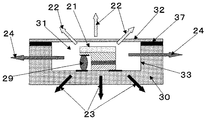
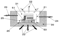
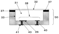
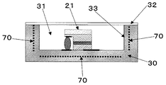
上記窪み空間を有する発光素子搭載用基板において、窪み空間を形成する方法として一体化したセラミック材料を主成分とする焼結体を用いて窪み空間を形成する方法、平板状の基体に枠体を接合することで窪み空間を形成する方法がある。本発明において上記窪み空間を有する発光素子搭載用基板としては、一体化したセラミック材料を主成分とする焼結体を用いて窪み空間を形成したもの、あるいは平板状の基体に他の材料例えば透明樹脂あるいはガラスからなる枠体を接合して窪み空間を形成したもの、という構成のものが好ましい。前記構成により本発明による発光素子搭載用基板はより発光素子からの発光を外部に放出し易くなるばかりでなく放熱性が高まり、電気回路がよりコンパクトに設計でき、大型の発光素子が搭載できる。上記平板状の基体に枠体を接合することで窪み空間が形成された発光素子搭載用基板において発光素子は通常上記平板状の基体に搭載される。本発明において上記窪み空間を有する発光素子搭載用基板において、平板状の基体と枠体との接合により窪み空間が形成されたものでは平板状の基体及び枠体のうちいずれか一方がセラミック材料を主成分とする焼結体からなるか、あるいは平板状の基体及び枠体いずれもセラミック材料を主成分とする焼結体からなる。上記平板状の基体あるいは枠体には必要に応じて発光素子を駆動させるための多層化メタライズや厚膜メタライズあるいは薄膜メタライズなどの電気回路、さらに導通ビアが具備される。
上記平板状の基体あるいは枠体の材料としてセラミック材料を主成分とする焼結体以外では、例えば各種金属、各種樹脂、各種ガラス、各種セラミックなど必要に応じて使用できる。
また、本発明による上記窪み空間を有する発光素子搭載用基板には必要に応じて窪み空間に搭載された発光素子を封止するための蓋が形成される。該蓋を用いた封止は封止材に金属、合金、ガラスを用いた気密封止あるいは封止材に樹脂などを用いた非気密封止のいずれも行うことができる。該蓋の材料として例えば各種金属、各種樹脂、各種ガラス、各種セラミックなどが使用できる。蓋に本発明による光透過性のあるセラミック材料を主成分とする焼結体や、他の透明樹脂やガラスあるいはセラミックなどを用いることで発光素子からの発光を効率よく基板外部に放出できる。本発明による発光素子搭載用基板には上記にように蓋として光透過性のあるセラミック材料を主成分とする焼結体を用いたものも含まれる。
In the substrate for mounting a light emitting element having the above-described hollow space, as a method for forming the hollow space, a method of forming the hollow space using a sintered body mainly composed of an integrated ceramic material, a frame body on a flat substrate There is a method of forming a hollow space by bonding. In the present invention, the substrate for mounting a light emitting element having the hollow space is one in which the hollow space is formed using a sintered body mainly composed of an integrated ceramic material, or another material such as a transparent substrate. A structure in which a hollow space is formed by joining frame bodies made of resin or glass is preferable. With the above-described structure, the light emitting element mounting substrate according to the present invention not only facilitates the emission of light emitted from the light emitting element to the outside, but also increases heat dissipation, allows the electric circuit to be designed more compactly, and allows a large light emitting element to be mounted. In a light emitting element mounting substrate in which a hollow space is formed by joining a frame to the flat substrate, the light emitting element is usually mounted on the flat substrate. In the present invention, in the light emitting element mounting substrate having the depression space, in which the depression space is formed by joining the flat substrate and the frame, one of the flat substrate and the frame is made of a ceramic material. Either a sintered body having a main component or a flat substrate and a frame are both formed of a sintered body having a ceramic material as a main component. The flat substrate or frame body is provided with an electric circuit such as multilayer metallization, thick film metallization, or thin film metallization for driving the light emitting element as necessary, and a conductive via.
Other than the sintered body whose main component is a ceramic material as the material of the flat substrate or frame, for example, various metals, various resins, various glasses, various ceramics and the like can be used as necessary.
In addition, a lid for sealing the light emitting element mounted in the hollow space is formed on the light emitting element mounting substrate having the hollow space according to the present invention, if necessary. Sealing using the lid can be performed either hermetic sealing using a metal, an alloy or glass as a sealing material, or non-hermetic sealing using a resin or the like as a sealing material. Examples of the material for the lid include various metals, various resins, various glasses, various ceramics, and the like. Light emitted from the light-emitting element can be efficiently emitted to the outside of the substrate by using a sintered body mainly composed of the light-transmitting ceramic material according to the present invention or other transparent resin, glass, or ceramic for the lid. The substrate for mounting a light emitting element according to the present invention includes a substrate using a sintered body whose main component is a light-transmitting ceramic material as described above.
本発明による発光素子搭載用基板に搭載あるいは収納される発光素子としては通常紫外光領域〜可視光〜近赤外光領域において発光機能を有するものであればどのようなものでも搭載し得る。具体的には例えば波長およそ200nm〜800nmの範囲の光を発光し得るものであればどのような発光素子であっても搭載し得る。例えばZnO系などの材料を主成分とする波長およそ380nm〜550nm付近の可視光領域の光を発光するものあるいはZnCdSe系などの材料を主成分とする波長およそ450nm〜650nm付近の可視光領域の光を発光するものあるいはAlGaInP系などの材料を主成分とする波長およそ600nm〜660nm付近の可視光領域の光を発光するものあるいはAlGaAs系などの材料を主成分とする波長およそ760nm〜820nm付近の可視光〜近赤外光領域の光を発光するものものなど各種材料からなる発光素子が搭載し得る。本発明による発光素子搭載用基板を用いることにより本来の発光特性が十分発現された発光素子が実現し得る。すなわち、光透過性を有するセラミック材料を主成分とする焼結体からなる基板に搭載された発光素子、及び反射防止部材が形成されたセラミック材料を主成分とする焼結体からなる基板に搭載された発光素子、及び反射部材が形成されたセラミック材料を主成分とする焼結体からなる基板に搭載された発光素子、である。 As the light emitting element to be mounted or housed on the light emitting element mounting substrate according to the present invention, any light emitting element having a light emitting function in the normal ultraviolet light region to visible light region to near infrared light region can be mounted. Specifically, any light-emitting element can be mounted as long as it can emit light having a wavelength in the range of approximately 200 nm to 800 nm. For example, light that emits light in the visible light region with a wavelength of approximately 380 nm to 550 nm mainly composed of a material such as ZnO or light in the visible light region that has a wavelength of approximately 450 nm to 650 nm mainly composed of a material such as ZnCdSe. That emits light in the visible light region with a wavelength of approximately 600 nm to 660 nm mainly composed of a material such as an AlGaInP material, or visible with a wavelength of approximately 760 nm to 820 nm mainly composed of an AlGaAs material or the like. Light emitting elements made of various materials such as those that emit light in the light to near infrared light region can be mounted. By using the light emitting element mounting substrate according to the present invention, a light emitting element in which the original light emission characteristics are sufficiently expressed can be realized. In other words, a light-emitting element mounted on a substrate made of a sintered body whose main component is a light-transmitting ceramic material, and a substrate made of a sintered body whose main component is a ceramic material on which an antireflection member is formed. And a light emitting element mounted on a substrate made of a sintered body mainly composed of a ceramic material on which a reflecting member is formed.
本発明による発光素子搭載用基板としては上記発光素子の中で窒化ガリウム、窒化インジウム、窒化アルミニウムのうちから選ばれた少なくとも1種以上を主成分とし少なくともN型半導体層、発光層、及びP型半導体層の3層以上の積層体からなる発光素子を搭載するのにより適している。該窒化ガリウム、窒化インジウム、窒化アルミニウムのうちから選ばれた少なくとも1種以上を主成分とする発光素子は波長200nm〜700nm程度の範囲の光を発光し得る。なお、以下本発明において特に断らない限り上記「窒化ガリウム、窒化インジウム、窒化アルミニウムのうちから選ばれた少なくとも1種以上を主成分とし少なくともN型半導体層、発光層、及びP型半導体層の3層以上の積層体からなる発光素子」を単に「窒化ガリウム、窒化インジウム、窒化アルミニウムのうちから選ばれた少なくとも1種以上を主成分とする発光素子」という。該窒化ガリウム、窒化インジウム、窒化アルミニウムのうちから選ばれた少なくとも1種以上を主成分とする発光素子は上記で例示した他の発光素子に比べて光出力も高く紫外光及び波長の短い可視光を発光することができ本発明による発光素子搭載用基板に搭載することで本来の発光特性が他の発光素子よりもさらに効果的に発現し得る。 The light-emitting element mounting substrate according to the present invention includes at least one selected from gallium nitride, indium nitride, and aluminum nitride as a main component among the light-emitting elements, and at least an N-type semiconductor layer, a light-emitting layer, and a P-type. It is more suitable to mount a light emitting element composed of a laminate of three or more semiconductor layers. A light-emitting element containing at least one selected from gallium nitride, indium nitride, and aluminum nitride as a main component can emit light in a wavelength range of about 200 nm to 700 nm. Unless otherwise specified in the present invention, at least one of at least one selected from gallium nitride, indium nitride, and aluminum nitride as a main component and at least an N-type semiconductor layer, a light-emitting layer, and a P-type semiconductor layer. A “light-emitting element composed of a laminate of two or more layers” is simply referred to as “a light-emitting element mainly composed of at least one selected from gallium nitride, indium nitride, and aluminum nitride”. A light-emitting element containing at least one selected from gallium nitride, indium nitride, and aluminum nitride as a main component has higher light output and visible light having a shorter ultraviolet light and wavelength than the other light-emitting elements exemplified above. By mounting on the light emitting element mounting substrate according to the present invention, the original light emission characteristics can be more effectively expressed than other light emitting elements.
上記窒化ガリウム、窒化インジウム、窒化アルミニウムのうちから選ばれた少なくとも1種以上を主成分とする発光素子は通常例えば図1あるいは図2に示されるような構造を有する。図1は、サファイアあるいは窒化アルミニウムを主成分とする単結晶や焼結体などの電気絶縁性の発光素子作製用基板1にMOCVDなどの方法によりエピタキシャル成長した窒化ガリウム、窒化インジウム、窒化アルミニウムのうちから選ばれた少なくとも1種以上を主成分としさらにSiなどのドーピング剤によりN型半導体化された薄膜層2が形成され、さらにエピタキシャル成長した窒化ガリウム、窒化インジウム、窒化アルミニウムのうちから選ばれた少なくとも1種以上を主成分とする例えば単一量子井戸構造、多重量子井戸構造あるいはダブルへテロ構造などからなる発光層3が形成され、さらにエピタキシャル成長した窒化ガリウム、窒化インジウム、窒化アルミニウムのうちから選ばれた少なくとも1種以上を主成分としさらにMg、Znなどのドーピング剤によりP型半導体化された薄膜層4が形成され、N型半導体薄膜層及びP型半導体薄膜層にはそれぞれ外部電極5及び6が形成されている発光素子の断面構造を示す。図1に示す発光素子において薄膜層2はP型半導体層としても形成することができ、その場合薄膜層4はN型半導体層として形成される。図1に示されるように発光素子を作製するための基板として電気絶縁性のものを用いた場合通常は外部電極5及び6は素子の形成されている面側に配置される。図2は炭化珪素を主成分とする単結晶あるいは窒化ガリウムを主成分とする単結晶や焼結体あるいは酸化亜鉛を主成分とする単結晶や焼結体など導電性を有する発光素子作製用基板10にMOCVDなどの方法によりエピタキシャル成長した窒化ガリウム、窒化インジウム、窒化アルミニウムのうちから選ばれた少なくとも1種以上からなる主成分にSiなどのドーピング剤などによりN型半導体薄膜層2が形成され、さらに上記窒化ガリウム、窒化インジウム、窒化アルミニウムのうちから選ばれた少なくとも1種以上を主成分とする量子井戸構造を有する発光層3が形成され、さらに窒化ガリウム、窒化インジウム、窒化アルミニウムのうちから選ばれた少なくとも1種以上からなる主成分にMgなどのドーピング剤によりP型半導体薄膜層4が形成され、N型半導体薄膜層及びP型半導体薄膜層にはそれぞれ外部電極5及び6が形成されている発光素子の断面構造を示す。図2に示す発光素子において薄膜層2はP型半導体層としても形成することができ、その場合薄膜層4はN型半導体層として形成される。図2に示されるように発光素子を作製するための基板として導電性のものを用いた場合通常電極5は発光素子を形成するための基板10の素子が形成されている面と反対側の面に形成でき一方の電極6は素子の形成されている面側に配置できる。図2の基板10には上記のように炭化珪素を主成分とする単結晶あるいは窒化ガリウムを主成分とする単結晶や焼結体あるいは酸化亜鉛を主成分とする単結晶や焼結体など元来導電性を有する材料だけでなく、窒化アルミニウムなど電気絶縁性の材料であっても発光素子を形成するための基板内部に導通ビアが形成され該基板の発光素子が形成される面とその反対側の面とが電気的に接続可能なものも含まれる。なお、図1及び図2において基板1あるいは基板10とエピタキシャル成長したN型半導体(あるいはP型)の薄膜層2との間には通常窒化ガリウム、窒化インジウム、窒化アルミニウムのうちから選ばれた少なくとも1種 以上を主成分とする薄膜バッファ層が形成される。バッファ層は通常低温で形成され無定形、多結晶、あるいは配向性多結晶などの結晶状態を有する場合が多い。なお、図2で示される発光素子作製用に用いられる導電性の基板10としては通常室温における抵抗率1×10⁴Ω・cm以下であれば上下に電極を配した形状の発光素子が作製でき十分機能し得る。導電性を有する発光素子作製用基板の室温における抵抗率としては室温において通常1×10²Ω・cm以下のものであれば少ない損失で十分な電力を発光層に供給し得る。導電性を有する発光素子作製用基板の室温における抵抗率としては室温において1×101Ω・cm以下のものが好ましく、1×100Ω・cm以下のものがより好ましく、1×10⁻¹Ω・cm以下のものがさらに好ましく、1×10⁻²Ω・cm以下のものが最も好ましい。
A light-emitting element containing at least one selected from gallium nitride, indium nitride, and aluminum nitride as a main component usually has a structure as shown in FIG. FIG. 1 shows gallium nitride, indium nitride, and aluminum nitride epitaxially grown by a method such as MOCVD on a substrate 1 for producing an electrically insulating light-emitting element such as a single crystal or sintered body mainly composed of sapphire or aluminum nitride. At least one selected from gallium nitride, indium nitride, and aluminum nitride formed by epitaxially growing at least one selected from the main component and forming an N-type semiconductor with a doping agent such as Si. A light-emitting
本発明で言う「窒化ガリウム、窒化インジウム、窒化アルミニウムのうちから選ばれた少なくとも1種以上を主成分とする発光素子」とは上記のようにサファイアなどの基板上に窒化ガリウム、窒化インジウム、窒化アルミニウムのうちから選ばれた少なくとも1種以上を主成分とするエピタキシャル成長した薄膜をN型半導体層、発光層、P型半導体層となしこれらを積層して構成されたものであり、電極に直流電位を印加することで発光層から光が発せられる。発光の波長は該発光層の組成を調整することなどで例えば紫外線領域から可視光領域の広い波長範囲にわたって光を発することができる。具体的にいえば例えば200nm〜700nmの波長範囲の光を発することができ、通常250nm〜650nmの波長範囲の光を発するように作製されることが多い。上記発光素子は発光ダイオード(LED)あるいはレーザーダイオード(LD)として広く使用され始めている。
上記のような窒化ガリウム、窒化インジウム、窒化アルミニウムのうちから選ばれた少なくとも1種以上を主成分とするエピタキシャル成長した薄膜により構成される発光素子を作製するために用いられる基板は従来から用いられてきたサファイアなどのような単結晶よりも、窒化アルミニウムを主成分とする焼結体あるいは炭化珪素、窒化珪素、窒化ガリウム、酸化亜鉛、酸化ベリリウム、酸化アルミニウムのうちから選ばれた少なくともいずれかを主成分とする焼結体、さらに酸化ジルコニウム、酸化マグネシウム、アルミン酸マグネシウム、酸化イットリウムなどの希土類元素酸化物、酸化トリウム、ムライト、結晶化ガラス、などのうちから選ばれた少なくともいずれかを主成分とする焼結体など各種セラミック材料を主成分とする焼結体の方が、発光効率が少なくとも同等か最大4〜5倍以上の発光素子が作製され得ることを本願発明者は特願2003−186175、特願2003−396236などで提案してきた。上記各種セラミック材料を主成分とする焼結体を基板として用いて作製される発光素子はサファイアなど従来からの基板を用いて作製される発光素子の発光効率が2%〜8%程度であるのに対して発光効率が少なくとも同等の8%かそれ以上、最大4〜5倍以上のものが作製でき50%以上の発光効率を有する発光素子も作製できる。発明による発光素子搭載用基板には本願発明者が提案したこのような高い発光効率を有する発光素子も問題なく搭載できる。
少なくとも図1及び図2に例示された構造の発光素子は発光層から波長800nm以下、通常波長650nm以下さらに波長550nm以下の緑色光〜波長200nmまでの紫外光といった波長範囲の光を発光し、該発光素子の発光層からは通常あらゆる方向に上記波長範囲の光が発せられる。本発明による発光素子搭載用基板はこのような発光素子を搭載あるいは収納するためのものである。
In the present invention, “a light-emitting element mainly composed of at least one selected from gallium nitride, indium nitride, and aluminum nitride” refers to gallium nitride, indium nitride, nitride on a substrate such as sapphire as described above. An epitaxially grown thin film mainly composed of at least one selected from aluminum is formed as an N-type semiconductor layer, a light-emitting layer, and a P-type semiconductor layer, and these are stacked, and a direct current potential is applied to an electrode. Is applied to emit light from the light emitting layer. The light emission wavelength can be emitted over a wide wavelength range from, for example, the ultraviolet region to the visible light region by adjusting the composition of the light emitting layer. Specifically, for example, it is possible to emit light in a wavelength range of 200 nm to 700 nm, and is usually manufactured so as to emit light in a wavelength range of 250 nm to 650 nm. The light-emitting element has begun to be widely used as a light-emitting diode (LED) or a laser diode (LD).
A substrate used for producing a light-emitting element composed of an epitaxially grown thin film mainly composed of at least one selected from gallium nitride, indium nitride, and aluminum nitride as described above has been conventionally used. It is mainly made of a sintered body mainly composed of aluminum nitride or at least one selected from silicon carbide, silicon nitride, gallium nitride, zinc oxide, beryllium oxide, and aluminum oxide rather than a single crystal such as sapphire. The main component is at least one selected from the group consisting of sintered bodies, rare earth element oxides such as zirconium oxide, magnesium oxide, magnesium aluminate, yttrium oxide, thorium oxide, mullite, and crystallized glass. Mainly composed of various ceramic materials such as sintered body Towards body is, the present inventors that the emission efficiency is at least equal to or up to 4 to 5 times more light-emitting elements can be made has been proposed in such as Japanese Patent Application No. 2003-186175, Japanese Patent Application No. 2003-396236. A light emitting device manufactured using a sintered body mainly composed of the above various ceramic materials as a substrate has a light emitting efficiency of about 2% to 8% of a light emitting device manufactured using a conventional substrate such as sapphire. On the other hand, it is possible to produce a light emitting element having a luminous efficiency of at least 8% or more, and a maximum of 4 to 5 times or more, and a light emitting element having a luminous efficiency of 50% or more. The light emitting element mounting substrate according to the invention can also be mounted without any problem with such a light emitting element proposed by the present inventor and having such a high luminous efficiency.
At least the light emitting element having the structure illustrated in FIGS. 1 and 2 emits light in the wavelength range from green light to ultraviolet light having a wavelength of 800 nm or less, usually a wavelength of 650 nm or less, and further a wavelength of 550 nm or less from a light emitting layer to a wavelength of 200 nm, The light emitting layer of the light emitting element usually emits light in the above wavelength range in all directions. The substrate for mounting a light emitting element according to the present invention is for mounting or housing such a light emitting element.
本発明による発光素子搭載用基板の材料としては単にセラミック材料を主成分とする焼結体というだけでは十分ではない。セラミック材料を主成分とする焼結体は例えば窒化アルミニウムを主成分とする焼結体などのように元来熱伝導率が高く、電気絶縁性があり、さらに熱膨張率が発光素子の主成分である窒化ガリウム、窒化インジウム、窒化アルミニウムとほとんど一致しており、該発光素子からの発熱を効率よく基板外部へ逃がすのに好適であり、多層化メタライズや薄膜メタライズなどを用いてコンパクトな回路基板設計が可能であり、また発光素子の駆動に伴う急熱急冷にも耐え、さらに大型発光素子を搭載し収納することが可能なものが多い。セラミック材料を主成分とする焼結体としては窒化アルミニウムを主成分とする焼結体以外にもその他前記したように例えば炭化珪素、窒化珪素、窒化ガリウム、酸化亜鉛、酸化ベリリウム、酸化アルミニウム、酸化ジルコニウム、酸化マグネシウム、アルミン酸マグネシウム、酸化チタン、チタン酸バリウム、チタン酸ジルコン酸鉛、酸化イットリウムなどの希土類酸化物、酸化トリウム、各種フェライト、ムライト、フォルステライト、ステアタイト、結晶化ガラス、のうちから選ばれた少なくとも1種以上を主成分とする焼結体など各種セラミック材料を主成分とする焼結体も発光素子搭載用基板として好適に用いることができる。窒化アルミニウムを主成分とする焼結体は上記例示した各種セラミック材料を主成分とする焼結体の中で特に優れている。このようにセラミック材料を主成分とする焼結体は上記のように基板材料として良好な特性を有するが発光素子搭載用基板としては十分でない。すなわち、発光素子が搭載される基板としては該発光素子からの発光が基板の外部に効率よく放出されることが重要であり、基板材料として窒化アルミニウムを主成分とする焼結体をはじめとするセラミック材料を主成分とする焼結体がその他の面でいかに優れていても基板外部への発光素子からの発光を効率よく放出できなければ発光素子が搭載される基板としては十分でない。発光素子からの発光は通常あらゆる方向に放出される。従来、発光素子を搭載し収納するための基板は前記のアルマイト被覆し表面を絶縁化したアルミニウムなどの金属材料を主に用いていた。そのため発光素子を搭載あるいは収納するための基板において、発光素子が搭載あるいは収納されている面側からは発光素子搭載部分の反射率を高めたりあるいは該搭載部分の形状を工夫することで発光素子の発光が基板の外部に比較的効率よく放出される。一方、発光素子からの発光が基板を貫通して透過しにくいため発光素子が搭載あるいは収納されている基板の面と反対側の面からは発光素子からの発光が効率よく基板外部に放出されない。したがって従来からの基板では全体的にみると発光素子からの発光は必ずしも基板外部に効率よく放出されているとは言いがたい。セラミック材料を主成分とする焼結体においても同様に発光素子からの発光が基板外部に効率よく放出されなければ発光素子を搭載あるいは収納するための基板としては十分なものであるとは云えない。 As a material for the light emitting element mounting substrate according to the present invention, it is not sufficient to simply use a sintered body mainly composed of a ceramic material. A sintered body containing a ceramic material as a main component, for example, a sintered body containing aluminum nitride as a main component has high heat conductivity, is electrically insulating, and has a thermal expansion coefficient that is the main component of a light-emitting element. It is almost the same as gallium nitride, indium nitride, and aluminum nitride, and is suitable for efficiently releasing the heat generated from the light emitting element to the outside of the substrate, and is a compact circuit board using multilayer metallization or thin film metallization. Many can be designed, can withstand rapid heating and cooling caused by driving of the light emitting element, and can be mounted and accommodated with a large light emitting element. In addition to the sintered body mainly composed of aluminum nitride, the sintered body mainly composed of a ceramic material, for example, silicon carbide, silicon nitride, gallium nitride, zinc oxide, beryllium oxide, aluminum oxide, and oxidized as described above. Among rare earth oxides such as zirconium, magnesium oxide, magnesium aluminate, titanium oxide, barium titanate, lead zirconate titanate, yttrium oxide, thorium oxide, various ferrites, mullite, forsterite, steatite, crystallized glass A sintered body mainly composed of various ceramic materials such as a sintered body mainly composed of at least one selected from the above can also be suitably used as the light emitting element mounting substrate. The sintered body mainly composed of aluminum nitride is particularly excellent among the sintered bodies mainly composed of the various ceramic materials exemplified above. As described above, a sintered body mainly composed of a ceramic material has good characteristics as a substrate material as described above, but is not sufficient as a substrate for mounting a light emitting element. That is, it is important for the substrate on which the light emitting element is mounted that light emitted from the light emitting element is efficiently emitted to the outside of the substrate, including a sintered body mainly composed of aluminum nitride as a substrate material. No matter how excellent the sintered body mainly composed of a ceramic material is, if the light emitted from the light emitting element to the outside of the substrate cannot be efficiently emitted, it is not sufficient as a substrate on which the light emitting element is mounted. Light emitted from the light emitting element is usually emitted in all directions. Conventionally, a substrate for mounting and housing a light emitting element mainly uses a metal material such as aluminum with the above-described anodized coating and insulating the surface. Therefore, in the substrate for mounting or housing the light emitting element, the reflectance of the light emitting element mounting portion is increased from the surface side where the light emitting element is mounted or stored, or the shape of the mounting portion is devised to improve the shape of the light emitting element. Light emission is emitted to the outside of the substrate relatively efficiently. On the other hand, since light emitted from the light emitting element is difficult to penetrate through the substrate, light emitted from the light emitting element is not efficiently emitted from the surface opposite to the surface of the substrate on which the light emitting element is mounted or stored. Therefore, it cannot be said that the light emitted from the light emitting element is necessarily efficiently emitted outside the substrate with the conventional substrate as a whole. Similarly, a sintered body mainly composed of a ceramic material cannot be said to be sufficient as a substrate for mounting or housing a light-emitting element unless light emitted from the light-emitting element is efficiently emitted outside the substrate. .
本発明において、光透過性を有するセラミック材料を主成分とする焼結体を発光素子搭載用基板に用いることで発光素子からの発光は基板を透過して外部に放出され易くなるので効率よく基板外部に放出することが可能となる。
さらに、本発明は発光素子が搭載あるいは収納されている基板の面と反対側の面を含めて発光素子からの発光を基板周囲の空間の任意の方向に対して放出することが可能なセラミック材料を主成分とする焼結体からなる発光素子搭載用基板をも提供するものである。上記発光素子からの発光を基板周囲の空間の任意の方向に放出可能ということは、例えば発光素子からの発光が基板周囲のすべての空間に均等に近い強さで放出できる、あるいは基板周囲のすべての空間に放出されるが特定の方向の空間により強く放出できる、あるいは基板周囲のすべての空間には放出されないが特定の方向の空間により強く放出できる、あるいは基板周囲の特定の方向の空間に対してだけ放出できる、ことなどを意味する。本発明はこのように発光素子からの発光の方向を制御可能である光素子搭載用基板をも提供するものである。そのために本発明は基板を構成する材料としてセラミック材料を主成分とする焼結体として光透過性を有するものを用いることが有効である。該光透過性を有するセラミック材料を主成分とする焼結体を用いることで発光素子からの発光は基板を貫通するように透過し、発光素子が搭載あるいは収納されている面側からは勿論、発光素子が搭載あるいは収納されている基板の面と反対側の面からも発光素子からの発光が効率よく基板外部に放出されるように改善できる。また、本発明において発光素子からの発光の方向を制御可能である光素子搭載用基板として反射防止部材あるいは反射部材などとセラミック材料を主成分とする焼結体とを組み合わせたものも有効である。反射防止部材あるいは反射部材などとセラミック材料を主成分とする焼結体とを組み合わせて用いることで発光素子からの発光の方向制御比較的容易に行うことができるようになる。また上記反射防止部材あるいは反射部材と組み合わせるセラミック材料を主成分とする焼結体は光透過性を有するものを用いることで発光素子からの発光の方向制御をさらに容易かつ確実に行えるようになる。なお、上記反射防止部材あるいは反射部材は光透過率が1%より小さいかあるいは実質的に光透過性を有しないセラミック材料を主成分とする焼結体に形成してもその反射防止機能及び反射機能を発現し得る。
本発明による発光素子からの発光を基板周囲の空間の任意の方向に対して放出することが可能な発光素子搭載用基板として用いられるセラミック材料を主成分とする焼結体は、上記のように反射防止部材や反射部材などと組み合わせて用いれば必ずしも光透過性を有しないものであってもその機能を発現し得るが、発光素子からの発光方向を制御を容易にし該発光の基板外部への放出効率を高めるためにできれば光透過性を有し要すれば高い光透過率を有するものを用いることが好ましい。
In the present invention, since a sintered body mainly composed of a light-transmitting ceramic material is used for a light-emitting element mounting substrate, light emitted from the light-emitting element easily passes through the substrate and is easily emitted to the outside. It becomes possible to discharge to the outside.
Furthermore, the present invention provides a ceramic material capable of emitting light emitted from the light emitting element including a surface opposite to the surface of the substrate on which the light emitting element is mounted or accommodated in any direction in the space around the substrate. The present invention also provides a substrate for mounting a light emitting element made of a sintered body containing as a main component. The fact that light emitted from the light emitting element can be emitted in any direction in the space around the substrate means that, for example, light emitted from the light emitting element can be emitted with an intensity nearly equal to all spaces around the substrate, or all around the substrate. Can be emitted more strongly in the space in a specific direction, or can be emitted more strongly in the space in a specific direction that is not emitted in all the space around the substrate, or in a specific direction around the substrate It means that it can only be released. The present invention also provides an optical element mounting substrate that can control the direction of light emission from the light emitting element. Therefore, in the present invention, it is effective to use a light-transmitting sintered body mainly composed of a ceramic material as a material constituting the substrate. By using a sintered body whose main component is the light-transmitting ceramic material, light emission from the light-emitting element is transmitted through the substrate, and of course from the surface side on which the light-emitting element is mounted or accommodated. It can be improved that light emitted from the light emitting element can be efficiently emitted from the surface opposite to the surface of the substrate on which the light emitting element is mounted or stored. In the present invention, an optical element mounting substrate capable of controlling the direction of light emission from the light emitting element is also effective in combination of an antireflection member or a reflecting member and a sintered body mainly composed of a ceramic material. . By using a combination of an antireflection member or a reflecting member and a sintered body containing a ceramic material as a main component, the direction of light emission from the light emitting element can be controlled relatively easily. Further, the sintered body mainly composed of a ceramic material combined with the antireflection member or the reflection member is made of a light transmissive material, whereby the direction of light emitted from the light emitting element can be controlled more easily and reliably. Even if the antireflection member or the reflection member is formed in a sintered body mainly composed of a ceramic material having a light transmittance of less than 1% or substantially not transmitting light, the antireflection function and reflection Function can be expressed.
A sintered body mainly composed of a ceramic material used as a light emitting element mounting substrate capable of emitting light emitted from the light emitting element according to the present invention in an arbitrary direction in a space around the substrate is as described above. If it is used in combination with an antireflection member, a reflection member, etc., even if it does not necessarily have light transmission, its function can be expressed, but the light emission direction from the light emitting element can be easily controlled, and the light emission to the outside of the substrate In order to increase the emission efficiency, it is preferable to use a material having a light transmittance if necessary and a high light transmittance if necessary.
本発明による発光素子搭載用基板に用いるセラミック材料を主成分とする焼結体は光透過性を有するものである。しかしながら本発明によるセラミック材料を主成分とする焼結体の光透過性とガラスや樹脂などの材料の光透過性とは性状が異なる。すなわち、例えば光透過率が80%と同じものであってもガラスや樹脂などの材料は照射された光が直線的に透過していくのに対して本発明によるセラミック材料を主成分とする焼結体の場合は照射された光は該焼結体の中を直線的に透過されることは少なく大部分は散乱されながら透過し結果として透過した光の総量はガラスや樹脂材料と同じになる。同じ光透過率の材料であっても光透過の経路が異なるものであれば透過された光の人間の目による視覚的な感じ方に違いが生じるものと思われる。すなわち発光素子からの光は透明樹脂や透明ガラスなどに対しては直線的に透過して目を突き刺す輝くような光として人間の目は感じ易く、一方セラミック材料を主成分とする焼結体の場合は散乱しながら透過するのでガラスや樹脂材料と比べて穏やかな光として人間の目には感じ易いと思われる。この様子を図28及び図29の模式図で示した。図28には光透過性を有するガラスあるいは樹脂など光が直線的に透過する材料を用いた時の光透過の様子を示す模式図である。図28において光透過性を有するガラスあるいは樹脂などの材料110に発光素子からの光111が照射されそのまま直線的に透過光112となって透過する。図29には光透過性を有するセラミック材料を主成分とする焼結体を光が透過する時の様子を示す模式図である。図29において光透過性を有するセラミック材料を主成分とする焼結体120に発光素子からの光121が照射され散乱光122となって透過する。
The sintered body mainly composed of a ceramic material used for the light emitting element mounting substrate according to the present invention is light transmissive. However, the light transmittance of the sintered body mainly composed of the ceramic material according to the present invention is different from the light transmittance of a material such as glass or resin. That is, for example, even if the light transmittance is the same as 80%, materials such as glass and resin transmit the irradiated light linearly, whereas the ceramic material according to the present invention is the main component. In the case of a bonded body, the irradiated light is hardly transmitted linearly through the sintered body, and most of the light is scattered while being transmitted. As a result, the total amount of transmitted light is the same as that of glass or resin material. . Even if the materials have the same light transmittance, if the light transmission paths are different, it is considered that a difference in how the transmitted light is visually perceived by the human eye is likely to occur. In other words, the light from the light emitting element is linearly transmitted to transparent resin or transparent glass, and the human eye can easily perceive it as shining light that pierces the eye, while the sintered body mainly composed of a ceramic material. In some cases, the light is transmitted while being scattered, so it is likely to be felt by human eyes as gentle light compared to glass or resin materials. This situation is shown in the schematic diagrams of FIGS. FIG. 28 is a schematic view showing a state of light transmission when a material that transmits light linearly, such as light-transmitting glass or resin, is used. In FIG. 28, light 111 from a light-emitting element is irradiated onto a light-transmitting
また上記セラミック材料を主成分とする焼結体として例えば黒色、灰黒色、灰色、褐色、黄色、緑色、青色、あずき色、赤色などに着色したものも用いることができる。このような着色したセラミック材料を主成分とする焼結体を透過した発光素子からの発光を穏やかな光として人間の目には感じ易くなる。例えば黒色、灰黒色、灰色、褐色、黄色、緑色、青色、あずき色、赤色などに着色したセラミック材料を主成分とする焼結体を透過した発光素子からの発光は黒色、灰黒色、灰色、褐色、黄色、緑色、青色、あずき色、赤色などに着色していない例えば白色などのセラミック材料を主成分とする焼結体を透過した光と比べて異なる光調の穏やかな光として人間の目には感じ易い。したがって用途によっては白色など着色していないセラミック材料を主成分とする焼結体よりも上記着色したセラミック材料を主成分とする焼結体を発光素子搭載用基板として用いることが好ましい場合がある。ここで異なる光調という意味は目で感じる光の感じ方が異なるということであり、セラミック材料を主成分とする焼結体の色調が異なれば焼結体を透過する光の輝き方、穏やかさの程度、色調などの要因が少しずつ異なる結果発光素子からの発光は実際の目での感じ方が微妙に違ってくるものと思われる。上記黒色、灰黒色、灰色、褐色、黄色、緑色、青色、あずき色、赤色などに着色したセラミック材料を主成分とする焼結体として例えばMo、W、V、Nb、Ta、Tiなどの遷移金属、あるいはカーボンなどの成分を含むものが用いられる。また、黒色、灰黒色、灰色、褐色、黄色、緑色、青色、あずき色、赤色などに着色したセラミック材料を主成分とする焼結体としてその他の遷移金属例えば鉄、ニッケル、クロム、マンガン、ジルコニウム、ハフニウム、コバルト、銅、亜鉛などの成分を含むものも用いられる。上記黒色、灰黒色、灰色、褐色、黄色、緑色、青色、あずき色、赤色など着色したセラミック材料を主成分とする焼結体を得るために用いられるMo、W、V、Nb、Ta、Ti、カーボン、鉄、ニッケル、クロム、マンガン、ジルコニウム、ハフニウム、コバルト、銅、亜鉛などの成分は、該セラミック材料を主成分とする焼結体を製造するときに意図的に加えられたものであっても良いし焼結体作製用原料中など不可避不純物として混入してくるものであっても良い。また、上記黒色、灰黒色、灰色、褐色、黄色、緑色、青色、あずき色、赤色など着色したセラミック材料を主成分とする焼結体にはMo、W、V、Nb、Ta、Ti、鉄、ニッケル、クロム、マンガン、ジルコニウム、ハフニウム、コバルト、銅、亜鉛などの遷移金属、あるいはカーボンなどの各成分をそれぞれ1種ずつ単独で含まれていてもよいしあるいは2種以上が同時に含まれていてもよい。上記黒色、灰黒色、灰色、褐色、黄色、緑色、青色、あずき色、赤色など着色したセラミック材料を主成分とする焼結体に含まれるMo、W、V、Nb、Ta、Ti、鉄、ニッケル、クロム、マンガン、ジルコニウム、ハフニウム、コバルト、銅、亜鉛などの遷移金属、あるいはカーボンなどの各成分の含有量は適宜選択することができ、含有量として通常0.1ppm〜1ppm以上であればセラミック材料を主成分とする焼結体を十分所望の着色されたものとすることが可能な場合が多い。このように通常上記各成分の種類とその含有量によりセラミック材料を主成分とする焼結体に対して所望の着色とその呈色の程度を制御し得る。例えば酸化アルミニウムを主成分とする焼結体にクロム成分を0.1ppm〜1.0ppm程度あるいはそれ以上含むものはピンク色あるいは赤色あるいはあずき色あるいは黒色などに呈色したものが得られ易い。 In addition, as a sintered body containing the ceramic material as a main component, for example, a sintered body colored black, gray-black, gray, brown, yellow, green, blue, maroon, red, or the like can be used. Light emitted from the light-emitting element that has passed through the sintered body containing such a colored ceramic material as a main component is easily perceived by human eyes as gentle light. For example, light emission from a light emitting element that has passed through a sintered body mainly composed of a ceramic material colored in black, gray black, gray, brown, yellow, green, blue, maroon, red, etc. is black, gray black, gray, Human eyes as gentle light with a different light intensity compared to light transmitted through a sintered body mainly composed of a ceramic material such as white that is not colored brown, yellow, green, blue, maroon, red, etc. Easy to feel. Therefore, in some applications, it may be preferable to use a sintered body mainly composed of the colored ceramic material as a light emitting element mounting substrate rather than a sintered body mainly composed of an uncolored ceramic material such as white. The meaning of the different light tones here is that the way the light is perceived by the eyes is different. If the color tone of the sintered body mainly composed of a ceramic material is different, the way the light passes through the sintered body and the gentleness As a result, the light emission from the light emitting element seems to be slightly different from the actual feeling. For example, Mo, W, V, Nb, Ta, Ti, etc. as a sintered body whose main component is a ceramic material colored in black, grayish black, gray, brown, yellow, green, blue, maroon, red, etc. Those containing components such as metal or carbon are used. In addition, other transition metals such as iron, nickel, chromium, manganese, zirconium are used as sintered bodies mainly composed of ceramic materials colored in black, grayish black, gray, brown, yellow, green, blue, maroon, red, etc. Those containing components such as hafnium, cobalt, copper, and zinc are also used. Mo, W, V, Nb, Ta, Ti used to obtain a sintered body whose main component is a colored ceramic material such as black, grayish black, gray, brown, yellow, green, blue, maroon, red Components such as carbon, iron, nickel, chromium, manganese, zirconium, hafnium, cobalt, copper, and zinc were intentionally added when manufacturing a sintered body mainly composed of the ceramic material. It may be mixed as an inevitable impurity such as in a raw material for producing a sintered body. In addition, the sintered body mainly composed of a ceramic material colored such as black, gray-black, gray, brown, yellow, green, blue, maroon, red, etc. includes Mo, W, V, Nb, Ta, Ti, iron , Nickel, chromium, manganese, zirconium, hafnium, cobalt, copper, zinc and other transition metals, or each component such as carbon may be included alone or in combination of two or more. May be. Mo, W, V, Nb, Ta, Ti, iron contained in a sintered body mainly composed of a colored ceramic material such as black, gray-black, gray, brown, yellow, green, blue, maroon, red, etc. Content of each component, such as transition metals, such as nickel, chromium, manganese, zirconium, hafnium, cobalt, copper, zinc, or carbon, can be selected as appropriate, and the content is usually 0.1 ppm to 1 ppm or more. In many cases, a sintered body containing a ceramic material as a main component can be sufficiently colored. As described above, the desired coloring and the degree of coloration of the sintered body mainly composed of the ceramic material can be controlled by the type and content of each component. For example, if a sintered body containing aluminum oxide as a main component contains a chromium component of about 0.1 ppm to 1.0 ppm or more, a product colored in pink, red, maroon or black is easily obtained.
本発明による光透過性を有するセラミック材料を主成分とする焼結体からなる発光素子搭載用基板において、発光素子からの発光は該セラミック材料を主成分とする焼結体中をいったん透過した後基板外部に放出される場合が多い。上記セラミック材料を主成分とする焼結体は各種セラミック材料を主成分とする微結晶からなる多結晶体である。したがって発光素子からの発光は該セラミック材料を主成分とする焼結体中を透過する際焼結体中で散乱光となり易いので、基板外部へ放出される該発光素子からの発光は発光素子から発せられる直接の光でなくあらゆる方向を持っているので透明樹脂や透明ガラスなどを直線的に透過してきた目を突き刺す輝くような光とは異なり穏やかな光となり易い。したがって一般照明の光源として本発明による発光素子搭載用基板に搭載した発光素子を使用すれば人間の眼にやさしくかつ穏やかな光源が得られ易い。 In the light emitting element mounting substrate comprising a sintered body mainly composed of a light-transmitting ceramic material according to the present invention, light emitted from the light emitting element is once transmitted through the sintered body mainly composed of the ceramic material. Often released to the outside of the substrate. The sintered body mainly composed of the ceramic material is a polycrystalline body composed of microcrystals mainly composed of various ceramic materials. Therefore, since light emitted from the light emitting element is likely to be scattered light in the sintered body when passing through the sintered body mainly composed of the ceramic material, light emitted from the light emitting element emitted to the outside of the substrate is emitted from the light emitting element. Since it has all directions, not direct light emitted, it tends to be gentle light unlike shining light that pierces the eyes that have been transmitted linearly through transparent resin or transparent glass. Therefore, if the light emitting element mounted on the light emitting element mounting substrate according to the present invention is used as a light source for general illumination, a gentle and gentle light source for human eyes can be easily obtained.
本発明による発光素子搭載用基板表面にタングステンあるいはモリブデンあるいは銅などを主成分として同時焼成などにより形成されるメタライズ、いったん焼成して得られるセラミック材料を主成分とする焼結体に後から焼き付けて形成する厚膜メタライズ、スパッタあるいは蒸着あるいはイオンプレーティングなどによる薄膜メタライズ、などにより焼結体内部あるいは焼結体表面に電気回路が設けられていても、本発明による発光素子搭載用基板がセラミック材料を主成分とする焼結体であるため発光素子からの発光は上記のように散乱光となり易く該発光素子から発せられた光は形成されている電気回路からの損失を受けることが少なく該発光素子搭載用基板を透過した光として効率よく基板外部に放出され得る。すなわち基板内を透過して外部へ放出される発光素子からの発光は焼結体表面に形成されている電気回路の影などによる明るさの減少が生じにくい。
また本発明による発光素子搭載用基板は電気回路が基板の表面だけでなくセラミック材料を主成分とする基板の内部にタングステンあるいはモリブデンあるいは銅などを主成分に用いて同時焼成などにより単層あるいは多層メタライズによる電気回路、あるいは導通ビアが形成されているものも用いることができる。このように基板の内部に電気回路が形成されているものであっても、本発明による発光素子搭載用基板として光透過性を有するセラミック材料を主成分とする焼結体を用いられるため発光素子からの発光は散乱光となり易く該発光素子から発せられた光は形成されている電気回路、あるいは導通ビアからの損失を受けることが少なく基板を透過して効率よく基板外部に放出され得る。すなわち基板内を透過して外部へ放出される発光素子からの発光は焼結体内部に形成されている電気回路や導通ビアの影などによる明るさの減少が生じにくい。
上記のように、本発明による発光素子搭載用基板は電気回路が基板の表面だけでなくセラミック材料を主成分とする基板の内部にタングステンあるいはモリブデンあるいは銅などを主成分とした導電性材料を用いて同時焼成などにより単層あるいは多層メタライズによる電気回路、あるいは導通ビアが形成されているものも用いることができる。さらに本発明による発光素子搭載用基板は基板の表面に電気回路が形成され基板の内部にも同時にも電気回路が形成されているものも用いることができる。このように基板の表面に電気回路が形成され基板の内部にも同時にも電気回路が形成されているものであっても、本発明による発光素子搭載用基板として光透過性を有するセラミック材料を主成分とする焼結体を用いれば発光素子からの発光は散乱光となり易いので該発光素子から発せられた光は形成されている電気回路、あるいは導通ビアからの損失を受けることが少なく基板を透過した光として効率よく基板外部に放出され得る。すなわち基板内を透過して外部へ放出される発光素子からの発光は焼結体内部あるいは焼結体表面に形成されている電気回路や導通ビアの影などによる明るさの減少が生じにくい。
The metallization formed on the surface of the light-emitting element mounting substrate according to the present invention by simultaneous firing mainly containing tungsten, molybdenum, copper, or the like, and later fired on a sintered body mainly comprising a ceramic material obtained by firing once. Even if an electric circuit is provided in the sintered body or on the surface of the sintered body by thick film metallization to be formed, thin film metallization by sputtering or vapor deposition or ion plating, etc., the light emitting element mounting substrate according to the present invention is a ceramic material. As described above, the light emitted from the light emitting element is easily scattered light as described above, and the light emitted from the light emitting element is less susceptible to loss from the formed electric circuit. It can be efficiently emitted outside the substrate as light transmitted through the element mounting substrate. That is, light emission from the light emitting element that is transmitted through the substrate and emitted to the outside is less likely to cause a decrease in brightness due to a shadow of an electric circuit formed on the surface of the sintered body.
The substrate for mounting a light emitting element according to the present invention is not limited to the surface of the substrate, but the inside of the substrate mainly composed of a ceramic material is used as a main component, tungsten, molybdenum, copper, etc. It is also possible to use an electric circuit formed by metallization, or one having conductive vias formed therein. Thus, even if an electric circuit is formed inside the substrate, a light emitting element mounting substrate according to the present invention can use a sintered body mainly composed of a light-transmitting ceramic material as the light emitting element mounting substrate. The light emitted from the light source easily becomes scattered light, and the light emitted from the light emitting element is less likely to be lost from the formed electric circuit or conductive via, and can be efficiently transmitted to the outside of the substrate through the substrate. That is, light emission from the light emitting element that is transmitted through the substrate and emitted to the outside is less likely to cause a decrease in brightness due to an electric circuit formed inside the sintered body or a shadow of a conductive via.
As described above, the light emitting element mounting substrate according to the present invention uses an electrically conductive material whose main component is tungsten, molybdenum, copper, or the like inside the substrate whose main component is a ceramic material as well as the surface of the substrate. It is also possible to use a single-layer or multi-layered metallized circuit or a conductive via formed by simultaneous firing. Furthermore, the light-emitting element mounting substrate according to the present invention may be one in which an electric circuit is formed on the surface of the substrate and an electric circuit is also formed inside the substrate. Thus, even if an electric circuit is formed on the surface of the substrate and an electric circuit is also formed inside the substrate at the same time, the light-transmitting ceramic material is mainly used as the light-emitting element mounting substrate according to the present invention. If a sintered body as a component is used, light emitted from the light emitting element is likely to be scattered light, so that the light emitted from the light emitting element is less likely to be lost from the formed electric circuit or conductive via and transmits through the substrate. The light can be efficiently emitted to the outside of the substrate. That is, light emitted from the light emitting element that is transmitted through the substrate and emitted to the outside is less likely to cause a decrease in brightness due to an electric circuit formed in the sintered body or on the surface of the sintered body, shadows of conductive vias, and the like.
図3、図4、図5、図6、図7、図8、図9、図10、図11、図12、図13、図14、図15、図16、図32及び図33、図36、図37、図38は本発明によるセラミック材料を主成分とする焼結体からなる発光素子搭載用基板を例示した断面図である。本発明において発光素子搭載用基板として用いられるセラミック材料を主成分とする焼結体は光透過性を有するものが好ましい。上記各図において少なくとも図3、図4、図5、図6、図7、図8、図9、図10は発光素子搭載用基板として用いられるセラミック材料を主成分とする焼結体が光透過性を有するものとして描かれている。また、図32、図33、図37及び図38は内部に電気回路が形成されたセラミック材料を主成分とする焼結体を用いて作製される発光素子搭載用基板を例示した断面図である。図36、図37及び図38にはさらに発光素子搭載部に素子からの発熱を基板外部へ放出するためのサーマルビアが形成されたものを示している。発光素子は必要に応じて透明樹脂などの封止材を用いて該封止材中に封止される。特に窪み空間を有しない平板状の発光素子搭載用基板を用いる場合、搭載される発光素子は上記封止材中に封止された状態で使用されることが好ましい。
また、図3、図4、図5、図6、図7、図8、図9、図10、図11、図12、図13、図14、図32、図33、図36及び図38は発光素子搭載用基板に搭載された状態の発光素子を例示している。
3, 4, 5, 6, 7, 8, 9, 10, 11, 12, 13, 14, 15, 16, 32, 33, and 36. 37 and 38 are cross-sectional views illustrating a light emitting element mounting substrate made of a sintered body mainly composed of a ceramic material according to the present invention. In the present invention, the sintered body mainly composed of a ceramic material used as the light emitting element mounting substrate preferably has light transmittance. 3, 4, 5, 6, 7, 8, 9, and 10 in each of the above drawings, a sintered body mainly composed of a ceramic material used as a light emitting element mounting substrate transmits light. It is drawn as having a sex. FIGS. 32, 33, 37 and 38 are cross-sectional views illustrating a light emitting element mounting substrate manufactured using a sintered body whose main component is a ceramic material in which an electric circuit is formed. . FIG. 36, FIG. 37, and FIG. 38 show a structure in which a thermal via for releasing heat generated from the element to the outside of the substrate is formed on the light emitting element mounting portion. The light emitting element is sealed in the sealing material by using a sealing material such as a transparent resin as necessary. In particular, when a flat light emitting element mounting substrate having no hollow space is used, the light emitting element to be mounted is preferably used in a state of being sealed in the sealing material.
3, 4, 5, 6, 7, 8, 9, 10, 11, 12, 13, 14, 32, 33, 36, and 38 are The light emitting element in the state of being mounted on the light emitting element mounting substrate is illustrated.
図3において本発明によるセラミック材料を主成分とする焼結体からなる発光素子搭載用基板20に発光素子21が搭載され、基板20の発光素子搭載面に形成されている同時焼成によるメタライズあるいは厚膜メタライズあるいは薄膜メタライズなどによる表面電気回路26とワイヤ25で電気的に接続されている。基板20の発光素子が搭載されている面において発光素子21からの発光22は殆どさえぎられることなく基板外部に放出される。また、発光素子が搭載されている面と反対側においても発光素子21から発せられた光が基板20を透過した光23として基板外部に放出される。このように発光素子搭載用基板に同時焼成によるメタライズあるいは厚膜メタライズあるいは薄膜メタライズなどにより電気回路が設けられていても、本発明による発光素子搭載用基板がセラミック材料を主成分とする焼結体であるため発光素子からの発光は散乱光となり易いので該発光素子から発せられた光は形成されている電気回路からの損失を受けることが少なく基板20を透過した光23として効率よく基板外部に放出され得る。
また本発明による発光素子搭載用基板は電気回路が基板の表面だけでなくセラミック材料を主成分とする基板の内部にタングステンあるいはモリブデンあるいは銅などを主成分に用いて同時焼成などにより単層あるいは多層メタライズによる電気回路、あるいは導通ビアが形成されているものも用いることができる。このように基板の内部に電気回路が形成されているものであっても、本発明による発光素子搭載用基板がセラミック材料を主成分とする焼結体であるため発光素子からの発光は散乱光となり易いので該発光素子から発せられた光は形成されている電気回路、あるいは導通ビアからの損失を受けることが少なく基板20を透過した光23として効率よく基板外部に放出され得る。
なお、図3において発光素子21は図1で示した構造のものを例示した。
In FIG. 3, a
The substrate for mounting a light emitting element according to the present invention is not limited to the surface of the substrate, but the inside of the substrate mainly composed of a ceramic material is used as a main component, tungsten, molybdenum, copper, etc. It is also possible to use an electric circuit formed by metallization, or one having conductive vias formed therein. Thus, even if an electric circuit is formed inside the substrate, light emission from the light-emitting element is scattered light because the light-emitting element mounting substrate according to the present invention is a sintered body mainly composed of a ceramic material. Therefore, the light emitted from the light emitting element is less likely to be lost from the formed electric circuit or the conductive via, and can be efficiently emitted outside the substrate as the light 23 transmitted through the
In FIG. 3, the
図4において発光素子21は図1に示した構造のものが例示されている。発光素子21は図1に示した状態から上下反転した状態でセラミック材料を主成分とする焼結体からなる発光素子搭載用基板20に搭載されている。図4において発光素子21に形成されている外部電極のうちN型半導体層に接続されているものは基板20の発光素子搭載面側に形成されている同時焼成によるメタライズあるいは厚膜メタライズあるいは薄膜メタライズなどによる表面電気回路26と低融点ろう材や導電性接着剤などからなる非ワイヤ状の接続材料29により固定され電気的にも接続されている。さらに該発光素子21のP型半導体層に接続されている外部電極は基板20の発光素子搭載面側に形成されている同時焼成によるメタライズあるいは厚膜メタライズあるいは薄膜メタライズなどによる表面電気回路26と低融点ろう材や導電性接着剤などからなる非ワイヤ状の接続材料(図に示されていない)により固定され電気的にも接続されている。基板20の発光素子が搭載されている面側において該発光素子からの発光22は殆どさえぎられることなく基板外部に放出される。また、発光素子が搭載されている面と反対側においても発光素子から発せられた光が基板20を透過した光23として基板外部に放出される。このように発光素子搭載用基板に同時焼成によるメタライズあるいは厚膜メタライズあるいは薄膜メタライズなどにより電気回路が設けられていても、本発明による発光素子搭載用基板がセラミック材料を主成分とする焼結体であるため発光素子からの発光は散乱光となり易いので該発光素子から発せられた光は形成されている電気回路からの損失を受けることが少なく基板20を透過した光23として効率よく基板外部に放出され得る。
また本発明による発光素子搭載用基板は電気回路が基板の表面だけでなくセラミック材料を主成分とする基板の内部にタングステンあるいはモリブデンあるいは銅などを主成分に用いて同時焼成などにより単層あるいは多層メタライズによる電気回路、あるいは導通ビアが形成されているものも用いることができる。このように基板の内部に電気回路が形成されているものであっても、本発明による発光素子搭載用基板がセラミック材料を主成分とする焼結体であるため発光素子からの発光は散乱光となり易いので該発光素子から発せられた光は形成されている電気回路、あるいは導通ビアからの損失を受けることが少なく基板20を透過した光23として効率よく基板外部に放出され得る。
なお、図4において発光素子21は図1で示した構造のものを例示した。
上記非ワイヤ状の接続材料は通常低融点ろう材や導電性接着剤などからなるが、該接続材料の使用形態としては液状、ペースト状、球状、円柱状、角柱状などの状態のものが用いられる。
In FIG. 4, the
The substrate for mounting a light emitting element according to the present invention is not limited to the surface of the substrate, but the inside of the substrate mainly composed of a ceramic material is used as a main component, tungsten, molybdenum, copper, etc. It is also possible to use an electric circuit formed by metallization, or one having conductive vias formed therein. Thus, even if an electric circuit is formed inside the substrate, light emission from the light-emitting element is scattered light because the light-emitting element mounting substrate according to the present invention is a sintered body mainly composed of a ceramic material. Therefore, the light emitted from the light emitting element is less likely to be lost from the formed electric circuit or the conductive via, and can be efficiently emitted outside the substrate as the light 23 transmitted through the
In FIG. 4, the
The non-wire-like connection material is usually composed of a low melting point brazing material, a conductive adhesive, or the like, but the connection material is used in a liquid, paste-like, spherical, cylindrical, or prismatic state. It is done.
図5において発光素子21は図2に示した構造のものが例示されている。図5において本発明によるセラミック材料を主成分とする焼結体からなる発光素子搭載用基板20に発光素子21が搭載され発光素子21のN型半導体層に接続されている外部電極は基板20の発光素子搭載面側に形成されている同時焼成によるメタライズあるいは厚膜メタライズあるいは薄膜メタライズなどによる表面電気回路26と低融点ろう材や導電性接着剤などからなる非ワイヤ状の接続材料 (図に示されていない)により固定され電気的にも接続され、もう一方のP型の半導体層に接続されている外部電極は基板20の発光素子搭載面側に形成されている同時焼成によるメタライズあるいは厚膜メタライズあるいは薄膜メタライズなどによる表面電気回路26とワイヤ25で電気的に接続されている。基板20の発光素子が搭載されている面側において該発光素子からの発光22は殆どさえぎられることなく基板外部に放出される。また、発光素子が搭載されている面と反対側においても発光素子から発せられた光が基板20を透過した光23として基板外部に放出される。このように発光素子搭載用基板に同時焼成によるメタライズあるいは厚膜メタライズあるいは薄膜メタライズなどにより電気回路が設けられていても、本発明による発光素子搭載用基板がセラミック材料を主成分とする焼結体であるため発光素子からの発光は散乱光となり易いので該発光素子から発せられた光は形成されている電気回路からの損失を受けることが少なく基板20を透過した光23として効率よく基板外部に放出され得る。
また本発明による発光素子搭載用基板は電気回路が基板の表面だけでなくセラミック材料を主成分とする基板の内部にタングステンあるいはモリブデンあるいは銅などを主成分に用いて同時焼成などにより単層あるいは多層メタライズによる電気回路、あるいは導通ビアが形成されているものも用いることができる。このように基板の内部に電気回路が形成されているものであっても、本発明による発光素子搭載用基板がセラミック材料を主成分とする焼結体であるため発光素子からの発光は散乱光となり易いので該発光素子から発せられた光は形成されている電気回路、あるいは導通ビアからの損失を受けることが少なく基板20を透過した光23として効率よく基板外部に放出され得る。
In FIG. 5, the
The substrate for mounting a light emitting element according to the present invention is not limited to the surface of the substrate, but the inside of the substrate mainly composed of a ceramic material is used as a main component, tungsten, molybdenum, copper, etc. It is also possible to use an electric circuit formed by metallization, or one having conductive vias formed therein. Thus, even if an electric circuit is formed inside the substrate, light emission from the light-emitting element is scattered light because the light-emitting element mounting substrate according to the present invention is a sintered body mainly composed of a ceramic material. Therefore, the light emitted from the light emitting element is less likely to be lost from the formed electric circuit or the conductive via, and can be efficiently emitted outside the substrate as the light 23 transmitted through the
図6において発光素子21は図1に示した構造のものが例示されている。また発光素子搭載用基板は窪み空間を有するものである。発光素子21は図1に示した状態から上下反転した状態で発光素子搭載用基板30に搭載されている。図6における発光素子の搭載状態は図4に示した搭載状態と同様なものである。図6において本発明によるセラミック材料を主成分とする焼結体からなる発光素子搭載用基板30は発光素子を収納するための窪み空間(キャビティー)31を有している。窪み空間31には発光素子21が搭載され該発光素子21に形成されている外部電極のうちN型半導体層に接続されているものは基板20の発光素子搭載面側に形成されている同時焼成によるメタライズあるいは厚膜メタライズあるいは薄膜メタライズなどによる電気回路26と低融点ろう材や導電性接着剤などからなる非ワイヤ状の接続材料29により電気的に接続されている。さらに該発光素子21のP型半導体層に接続されている外部電極は基板20の発光素子搭載面側に形成されている同時焼成によるメタライズあるいは厚膜メタライズあるいは薄膜メタライズなどによる表面電気回路26と低融点ろう材や導電性接着剤などからなる非ワイヤ状の接続材料(図に示されていない)により電気的に接続されている。基板30の発光素子が搭載されている面側には必要に応じて窪み空間31に搭載されている発光素子を封止するために、蓋32がはんだ、ろう材、ガラス、樹脂などの封止材料により封止部37で発光素子搭載用基板30に取り付けられている。蓋32として光透過性のある窒化アルミニウムを主成分とする焼結体をはじめとする各種セラミック材料を主成分とする焼結体、あるいは透明なガラスや樹脂を用いることで該発光素子からの発光22は実質的に殆ど吸収されることなく基板外部に放出される。また、発光素子が搭載されている面と反対側においても発光素子から発せられた光が基板30を透過した光23として基板外部に放出される。さらに発光素子から発せられた光は窪み空間31の側壁33からも基板を透過した光24として基板外部に放出される。このように窪み空間を有する基板に同時焼成によるメタライズあるいは厚膜メタライズあるいは薄膜メタライズなどにより電気回路が設けられていても、本発明による発光素子搭載用基板がセラミック材料を主成分とする焼結体であるため発光素子からの発光は散乱光となり易いので該発光素子から発せられた光は形成されている電気回路からの損失を受けることが少なく基板30を透過した光23として効率よく基板外部に放出され得る。
また本発明による発光素子搭載用基板は電気回路が基板の表面だけでなくセラミック材料を主成分とする基板の内部にタングステンあるいはモリブデンあるいは銅などを主成分に用いて同時焼成などにより単層あるいは多層メタライズによる電気回路、あるいは導通ビアが形成されているものも用いることができる。このように基板の内部に電気回路が形成されているものであっても、本発明による発光素子搭載用基板がセラミック材料を主成分とする焼結体であるため発光素子からの発光は散乱光となり易いので該発光素子から発せられた光は形成されている電気回路、あるいは導通ビアからの損失を受けることが少なく基板30を透過した光23として効率よく基板外部に放出され得る。
本発明において発光素子搭載用基板が図6に示されるような窪み空間を有する場合においても発光素子としては図2に示した構造のものも搭載できる。また発光素子の搭載状態として、図3、あるいは図5に示したようなワイヤを用いる方法によっても本発明による発光素子搭載用基板に搭載できる。図6において窪み空間部分31を気密に封止するために設けられている蓋32は必ずしも必要でなく、かつ発光素子からの発光を損失なく基板外部に放出するために蓋32のない状態でも本発明の発光素子搭載用基板として使用できる。蓋32を設けない場合発光素子からの発光はまったく吸収されることなく基板外部に放出される。発光素子からの発光を損失なく基板外部に放出するためであれば蓋32を必ずしも透明な光透過性の材料を用いて設ける必要性はない。蓋を設けない場合図6における窪み空間部分31の部分に光透過性の樹脂(図6には表示していない)を充填することでも発光素子の封止が可能で、かつ発光素子からの発光を効率よく基板外部に放出できる。このような光透過性の蓋及び光透過性の樹脂に蛍光体などを加えることで発光素子からの発光を任意の色彩に変換可能である。
In FIG. 6, the
The substrate for mounting a light emitting element according to the present invention is not limited to the surface of the substrate, but the inside of the substrate mainly composed of a ceramic material is used as a main component, tungsten, molybdenum, copper, etc. It is also possible to use an electric circuit formed by metallization, or one having conductive vias formed therein. Even if an electric circuit is formed inside the substrate in this way, the light emitting element mounting substrate according to the present invention is a sintered body mainly composed of a ceramic material, so that light emitted from the light emitting element is scattered light. Therefore, the light emitted from the light emitting element is less likely to be lost from the formed electric circuit or the conductive via, and can be efficiently emitted to the outside as the light 23 transmitted through the
In the present invention, even when the light emitting element mounting substrate has a hollow space as shown in FIG. 6, the light emitting element having the structure shown in FIG. 2 can be mounted. Further, as a mounting state of the light emitting element, it can be mounted on the light emitting element mounting substrate according to the present invention by a method using a wire as shown in FIG. 3 or FIG. In FIG. 6, the
基板内部に導通ビア、あるいはタングステン、モリブデン、銅などを主成分として用いた同時焼成による単層又は多層化メタライズ、あるいは厚膜メタライズ、あるいは薄膜メタライズなどによる電気回路などが設けられた場合でも同じである。図7は板状の発光素子搭載用基板内部に導通ビアが設けられた場合を例示する。セラミック材料を主成分とする焼結体を用いて作製される発光素子搭載用基板20の内部には該基板の発光素子が搭載されている面とその反対側の面とを電気的に接続する導通ビア40が形成されている。導通ビア40を介して発光素子21と基板の発光素子搭載面と反対側に設けられた同時焼成メタライズや厚膜メタライズあるいは薄膜メタライズなどによる表面電気回路41とが電気的に接続されている。該電気回路41から発光素子21を駆動するための電力などが基板外部から供給される。図7で示した本発明による発光素子搭載用基板に同時焼成による単層又は多層化メタライズあるいは厚膜メタライズあるいは薄膜メタライズなどにより電気回路が設けられていても、該基板がセラミック材料を主成分とする焼結体であるため発光素子からの発光は散乱光となりやすいので実質的に電気回路からの損失を受けることなく該発光素子から発せられた光は基板20を透過した光23として基板外部に放出される。また、図7に示すように基板として導通ビアが形成されたものであっても、基板20の発光素子が搭載されている面側において該発光素子からの発光22は損失を受けることが少なく基板外部に放出され、さらに該発光素子から発せられた光が基板20を透過した光23として効率的に基板外部に放出されるという効果は同じである。
図7に例示された導通ビアだけでなく基板内部にタングステンあるいはモリブデンあるいは銅などを主成分とする単層又は多層化メタライズ、あるいは金、銀、銅、パラジウム、白金などを主成分とする厚膜メタライズ、あるいは薄膜メタライズなどにより電気回路が設けられた場合でも、発光素子が搭載されている面と反対側において発光素子から発せられた光が損失を受けることが少なく基板20を透過した光23として効率的に基板外部に放出されるという効果は同じである。本発明による発光素子搭載用基板においては導通ビア40により基板内部の電気回路と表面の電気回路とを接続してより複雑な電気回路を有するものも製造できる。
Even if a conductive via, or a single-layer or multi-layer metallization by simultaneous firing using tungsten, molybdenum, copper, etc. as the main component, or an electric circuit by a thick film metallization or a thin film metallization, etc. are provided inside the substrate. is there. FIG. 7 illustrates a case where a conductive via is provided inside a plate-shaped light emitting element mounting substrate. Inside the light emitting
In addition to the conductive vias illustrated in FIG. 7, a single-layer or multi-layer metallization containing tungsten, molybdenum, copper, or the like as a main component inside the substrate, or a thick film mainly containing gold, silver, copper, palladium, platinum, or the like. Even when an electric circuit is provided by metallization or thin film metallization, light emitted from the light-emitting element is less likely to be lost on the side opposite to the surface on which the light-emitting element is mounted. The effect of being efficiently released to the outside of the substrate is the same. In the substrate for mounting a light emitting element according to the present invention, a substrate having a more complicated electric circuit can be manufactured by connecting the electric circuit inside the substrate and the electric circuit on the surface by the conductive via 40.
また、窪み空間を有する基板の内部に導通ビアあるいは同時焼成による単層又は多層化メタライズあるいは厚膜メタライズあるいは薄膜メタライズなどによる電気回路が設けられた場合でも同じである。図8は窪み空間を有する発光素子搭載用基板内部に導通ビアが設けられた場合の状態を例示したものである。図8においてセラミック材料を主成分とする焼結体を用いて作製される窪み空間31を有する発光素子搭載用基板30の内部には基板の発光素子が搭載されている面とその反対側の面とを電気的に接続する導通ビア40が形成されている。導通ビア40を介して発光素子21と基板の発光素子搭載面と反対側に設けられた同時焼成メタライズ、あるいは厚膜メタライズ、あるいは薄膜メタライズなどによる表面電気回路41とが電気的に接続されている。また、図8に示すように基板として導通ビアが形成されたものであっても、基板30の発光素子が搭載されている面側において該発光素子からの発光22は損失を受けることが少なく基板外部に放出され、さらに該発光素子から発せられた光が基板30を透過した光23として効率的に基板外部に放出されるという効果は同じである。また、発光素子から発せられた光は窪み空間31の側壁33からも基板を透過した光24として基板外部に放出される。
図8に例示された導通ビアだけでなく基板内部にタングステンあるいはモリブデンあるいは銅などを主成分とする単層又は多層化メタライズ、あるいは金、銀、銅、パラジウム、白金などを主成分とする厚膜メタライズ、あるいは薄膜メタライズなどにより電気回路が設けられた場合でも、発光素子が搭載されている面と反対側において発光素子から発せられた光が損失を受けることが少なく基板30を透過した光23として効率的に基板外部に放出されるという効果は同じである。上記基板内部に導通ビア、タングステンあるいはモリブデンあるいは銅などを主成分として同時焼成などにより形成される単層あるいは多層化メタライズ、いったん焼成することで得られるセラミック材料を主成分とする焼結体に後から焼き付けて形成する厚膜メタライズ、スパッタあるいは蒸着あるいはイオンプレーティングなどによる薄膜メタライズ、などによる電気回路が設けられる部分には図8に例示したような基板底部だけでなく窪み空間の側壁部分も含まれる。本発明による発光素子搭載用基板においては導通ビア40により基板内部の電気回路と表面の電気回路とを接続してより複雑な電気回路を有するものも製造できる。
The same applies to the case where a conductive via, or a single-layer or multi-layer metallization by co-firing, a thick-film metallization, or a thin-film metallization is provided inside the substrate having a hollow space. FIG. 8 illustrates a state where a conductive via is provided inside the light emitting element mounting substrate having a hollow space. In FIG. 8, inside the light emitting
In addition to the conductive vias illustrated in FIG. 8, a single-layer or multi-layer metallization containing tungsten, molybdenum, copper, or the like as a main component inside the substrate, or a thick film containing gold, silver, copper, palladium, platinum, or the like as a main component. Even when an electric circuit is provided by metallization or thin film metallization, light emitted from the light-emitting element is less likely to be lost on the side opposite to the surface on which the light-emitting element is mounted. The effect of being efficiently released to the outside of the substrate is the same. A single layer or multi-layered metallization formed by co-firing with conductive vias, tungsten, molybdenum, or copper as the main component inside the substrate, and then sintered into a sintered body with a ceramic material as the main component obtained by firing once. 8 includes not only the bottom of the substrate as illustrated in FIG. 8 but also the side wall portion of the hollow space in the portion provided with the electric circuit by thick film metallization formed by baking, thin film metallization by sputtering or vapor deposition or ion plating, etc. It is. In the substrate for mounting a light emitting element according to the present invention, a substrate having a more complicated electric circuit can be manufactured by connecting the electric circuit inside the substrate and the electric circuit on the surface by the conductive via 40.
本発明による基板を実際発光素子搭載用として使用する場合の形態としては、上記図3〜図8で例示し説明してきたように1個の基板に発光素子を直接搭載する形態で用いることができる。
本発明による基板と発光素子との電気的接続は図3〜図8で示したワイヤによる方法、及び低融点ろう材や導電性接着剤など非ワイヤ状の接続材料を用いる方法をそれぞれ単独であるいはこれらの方法を組み合わせて行うことができる。また、発光素子を駆動するためのタングステンあるいはモリブデンあるいは銅などを主成分として同時焼成などにより形成される単層あるいは多層化メタライズ、いったん焼成することで得られるセラミック材料を主成分とする焼結体に後から焼き付けて形成する厚膜メタライズ、スパッタあるいは蒸着あるいはイオンプレーティングなどによる薄膜メタライズ、などによる電気回路は、図3〜図8で示したように基板の外部表面あるいは導通ビアなどと同様基板内部に設けることができる。これら基板表面及び基板内部の電気回路は導通ビアなどを適宜用いて単独で、あるいは同時に組み合わせて設けることができる。
As a form in which the substrate according to the present invention is actually used for mounting the light emitting element, it can be used in a form in which the light emitting element is directly mounted on one substrate as illustrated and described in FIGS. .
The electrical connection between the substrate and the light emitting device according to the present invention may be performed by using a wire method shown in FIGS. 3 to 8 and a method using a non-wire-like connection material such as a low melting point brazing material or a conductive adhesive. A combination of these methods can be performed. In addition, a single layer or multilayer metallization formed by simultaneous firing, etc. with tungsten, molybdenum, copper, or the like as a main component for driving a light emitting element, and a sintered body with a ceramic material as a main component obtained by firing once The electric circuit by thick film metallization formed by later baking, thin film metallization by sputtering or vapor deposition or ion plating, etc. is the same as the external surface of the substrate or the conductive via as shown in FIGS. It can be provided inside. These electric circuits on the substrate surface and inside the substrate can be provided singly or in combination using conductive vias as appropriate.
発光素子の大きさが1mm前後と比較的小さい場合や基板へ直接搭載することが困難な場合など、該発光素子の基板への実装性を高めるために該発光素子を一旦サブマウントに搭載した後本発明による基板に搭載することもできる。図9及び図10はサブマウントを用いて発光素子を搭載する場合の本発明による基板の使用形態の断面を示している。 After the light-emitting element is mounted on the submount in order to improve the mountability of the light-emitting element on the substrate, such as when the size of the light-emitting element is relatively small at around 1 mm or when it is difficult to directly mount it on the substrate. It can also be mounted on a substrate according to the present invention. FIG. 9 and FIG. 10 show a cross section of a usage pattern of a substrate according to the present invention when a light emitting element is mounted using a submount.
図9は発光素子21がサブマウント50にいったん搭載され該サブマウント50が本発明による基板20に搭載されている例が示されている。図9において発光素子21との発光素子搭載用基板20とはサブマウント50の表面に設けられている同時焼成メタライズ、あるいは厚膜メタライズ、あるいは薄膜メタライズなどによる電気回路51と基板20の発光素子搭載面側に設けられているタングステンあるいはモリブデンあるいは同などを主成分とする同時焼成メタライズ、いったん焼成することで得られるセラミック材料を主成分とする焼結体に後から焼き付けて形成する厚膜メタライズ、スパッタあるいは蒸着あるいはイオンプレーティングなどによる薄膜メタライズ、などによる表面電気回路26とをワイヤ25により接続することで電気的に接続されている。図9において基板20の発光素子が搭載されている面側において該発光素子からの発光22は殆どさえぎられることなく基板外部に放出される。また、発光素子が搭載されている面と反対側においても発光素子から発せられた光が基板20を透過した光23として基板外部に放出される。本発明においてサブマウント50として内部にタングステンあるいはモリブデンあるいは銅などを主成分として同時焼成などにより形成される単層あるいは多層化メタライズによる電気回路を有するものも用いることができる。
FIG. 9 shows an example in which the
図10は発光素子21がサブマウント50にいったん搭載され該サブマウント50が本発明による窪み空間31を有する発光素子搭載用基板30に搭載されている例が示されている。図10において発光素子21と発光素子搭載用基板30とはサブマウント50の表面に設けられているタングステンあるいはモリブデンあるいは同などを主成分とする同時焼成メタライズ、いったん焼成することで得られるセラミック材料を主成分とする焼結体に後から焼き付けて形成する厚膜メタライズ、スパッタあるいは蒸着あるいはイオンプレーティングなどによる薄膜メタライズ、などによる電気回路51と基板30の発光素子搭載面側に設けられている厚膜あるいは薄膜メタライズなどによる表面電気回路26とをワイヤ25により接続することで電気的に接続されている。図10において基板30の発光素子が搭載されている面側において該発光素子からの発光22は殆どさえぎられることなく基板外部に放出される。また、発光素子が搭載されている面と反対側においても発光素子から発せられた光が基板30を透過した光23として基板外部に放出される。また、発光素子から発せられた光は窪み空間31の側壁からも基板を透過した光24として基板外部に放出される。本発明においてサブマウント50として内部にタングステンあるいはモリブデンあるいは銅などを主成分として同時焼成などにより形成される単層あるいは多層化メタライズによる電気回路を有するものも用いることができる。
FIG. 10 shows an example in which the
サブマウントの形態は図9、図10に例示されたものだけではなく各種形態のものが使用できる。また、該サブマウントと本発明による基板との接続も図9、図10に例示されたものだけではなく各種方法が使用できる。図11及び図12にサブマウントの形態、及び該サブマウントと本発明による基板との接続状態の断面を例示した。 The form of the submount is not limited to those illustrated in FIGS. 9 and 10, and various forms can be used. The connection between the submount and the substrate according to the present invention is not limited to those illustrated in FIGS. 9 and 10, and various methods can be used. FIG. 11 and FIG. 12 illustrate the cross-section of the submount configuration and the connection state between the submount and the substrate according to the present invention.
図11はサブマウント50の側面に同時焼成メタライズや厚膜メタライズあるいは薄膜メタライズなどによる電気回路52が施されている例を示す。図11において発光素子21はサブマウント50にいったん搭載され該サブマウント50が本発明による発光素子搭載用基板20に搭載されている。図11において発光素子21と発光素子搭載用基板20とはサブマウント50の表面に設けられている電気回路51と基板20の発光素子搭載面側に設けられているタングステンあるいはモリブデンあるいは同などを主成分とする同時焼成メタライズ、いったん焼成することで得られるセラミック材料を主成分とする焼結体に後から焼き付けて形成する厚膜メタライズ、スパッタあるいは蒸着あるいはイオンプレーティングなどによる薄膜メタライズ、などによる表面電気回路26とをサブマウント側面の電気回路52により接続することで電気的に接続されている。本発明においてサブマウント50として内部にタングステンあるいはモリブデンあるいは銅などを主成分として同時焼成などにより形成される単層あるいは多層化メタライズによる電気回路を有するものも用いることができ導通ビア53により表面の電気回路と接続してより複雑な電気回路を形成できる。
FIG. 11 shows an example in which an
図12はサブマウント50の内部に導通ビア63が施されている例を示す。図12において発光素子21はサブマウント50にいったん搭載され該サブマウント50が本発明による発光素子搭載用基板20に搭載されている。図12において発光素子21と発光素子搭載用基板20とはサブマウント50の内部に設けられている導通ビア53と基板20の発光素子搭載面側に設けられているタングステンあるいはモリブデンあるいは同などを主成分とする同時焼成メタライズ、いったん焼成することで得られるセラミック材料を主成分とする焼結体に後から焼き付けて形成する厚膜メタライズ、スパッタあるいは蒸着あるいはイオンプレーティングなどによる薄膜メタライズ、などによる電気回路26とをサブマウント内部の導通ビア53により接続することで電気的に接続されている。本発明においてサブマウント50として内部にタングステンあるいはモリブデンあるいは銅などを主成分として同時焼成などにより形成される単層あるいは多層化メタライズによる電気回路を有するものも用いることができ導通ビア53により表面の電気回路と接続してより複雑な電気回路を形成できる。
FIG. 12 shows an example in which the conductive via 63 is provided inside the
本発明による発光素子搭載用基板に上記サブマウントを搭載する場合、基板は任意の形態のものを用いることができる。図9〜図12以外にも基板として内部に導通ビア、あるいはタングステン、モリブデン、銅などを主成分として同時焼成などにより形成される多層化メタライズ、いったん焼成することで得られるセラミック材料を主成分とする焼結体に後から焼き付けて形成する厚膜メタライズ、スパッタあるいは蒸着あるいはイオンプレーティングなどによる薄膜メタライズ、などを有するものなどを用いることができる。例えば、1)図13の符号20で示すような平板状で基板内部に導通ビア40を有するもの、2)図14の符号30で示すような窪み空間31を有しさらに基板内部に導通ビア40を有するもの、などの形態を有するものが使用できる。なお、図13及び図14は本発明による発光素子搭載用基板にサブマウントを介して発光素子が搭載されている様子を示す断面図である。
When the submount is mounted on the light emitting element mounting substrate according to the present invention, any substrate can be used. In addition to FIG. 9 to FIG. 12, conductive vias inside the substrate as a substrate, or multilayer metallization formed by simultaneous firing or the like with tungsten, molybdenum, copper or the like as a main component, ceramic material obtained by once firing as a main component It is possible to use a material having a thick film metallization formed by later baking on a sintered body to be formed, a thin film metallization by sputtering or vapor deposition, ion plating, or the like. For example, 1) a flat plate as shown by
また、サブマウントとして本発明による光透過性を有する窒化アルミニウムを主成分とする焼結体をはじめとする各種セラミック材料を主成分とする焼結体からなる発光素子搭載用基板を用いることができる。本発明による発光素子搭載用基板は光透過性を有するセラミック材料を主成分とする焼結体からなるが、本発明による発光素子搭載用基板をサブマウントとして用いることで発光素子からの発熱を効果的に逃がし、多層化メタライズや薄膜メタライズなどを用いてコンパクトなサブマウント基板が設計でき、発光素子の駆動に伴う急熱急冷にも耐え、さらに光透過性を有するなど、他の材料からなるサブマウントに比べて優れている。 In addition, a light-emitting element mounting substrate made of a sintered body mainly composed of various ceramic materials including a sintered body mainly composed of light-transmitting aluminum nitride according to the present invention can be used as the submount. . The light emitting element mounting substrate according to the present invention is made of a sintered body mainly composed of a light-transmitting ceramic material. However, the use of the light emitting element mounting substrate according to the present invention as a submount is effective in generating heat from the light emitting element. Sub-layers made of other materials such as multi-layer metallization and thin-film metallization can be used to design compact submount substrates, withstand rapid heating and quenching associated with driving light-emitting elements, and have light transmission properties. It is superior to the mount.
本発明による発光素子搭載用基板のうち発光素子が搭載されていない状態の窪み空間を有するものの断面図を図15及び図16に例示する。
図15において窪み空間を有する発光素子搭載用基板30は平板状の基体34、枠体35及びに蓋32より構成されている。平板状の基体34に枠体35が接合部36で接合されることで窪み空間31が形成されている。本発明において上記発光素子搭載用基板30において基体34あるいは枠体35のうちいずれか一方がセラミック材料を主成分とする焼結体からなるか、あるいは基体34あるいは枠体35のどちらもセラミック材料を主成分とする焼結体からなるか、いずれかである。また、基体34あるいは枠体35の材料としてセラミック材料を主成分とする焼結体以外に必要に応じて各種金属、合金、ガラス、セラミック、樹脂などを主成分とするものが使用できる。基体34あるいは枠体35の材料として透明なガラス、樹脂、セラミックなどを用いれば発光素子からの発光があまり損失を伴うことなく基板外部に放出できるので好ましい。また、基体34あるいは枠体35の材料として光を透過しにくい光不透過性の各種金属、合金、ガラス、セラミック、樹脂などを主成分とするものを用いればその部分では発光素子からの発光は基板を透過しにくくなるので該発光を基板外部に放出させたくない方向を制御するために用いれば有効に機能する。上記発光素子搭載用基板30において窪み空間を封止するための蓋32が取り付けられている。蓋32は通常発光素子を搭載した後に枠体に取り付け、その際蓋32は封止部37においてはんだ、ろう材、ガラス、樹脂などを主成分とする封止材料で発光素子を封止する。蓋32の材料として各種金属、合金、ガラス、セラミック、樹脂などを主成分とする材料が用いることができる。蓋32の材料として光透過性を有する窒化アルミニウムを主成分とする焼結体をはじめとする各種セラミック材料を主成分とする焼結体や透明なガラス、樹脂などを用いれば発光素子からの発光があまり損失を伴うことなく蓋から基板外部に放出できるので好ましい。また、蓋32の材料として光を透過しにくい光不透過性の各種金属、合金、ガラス、樹脂、などを主成分とするもの、あるいは各種セラミックを主成分とする焼結体(光を透過しにくい光不透過性の窒化アルミニウムを主成分とする焼結体などを含む)などを用いれば発光素子からの発光は蓋を透過しにくくなるので蓋が取り付けられる方向に該発光を放出させたくない場合には有効である。また、封止に際して蓋の材料として金属、合金、ガラス、各種セラミックを主成分とする焼結体など、封止材としてはんだ、ろう材、ガラスなどを用いれば気密封止が可能となる。また、なお蓋32は必要に応じて用いなくてもよい。その場合発光素子の封止は窪み空間31に透明な樹脂などを充填することで行うことができる。図15において基体34には導通ビア40、基板の外部表面に形成されている表面電気回路41、発光素子搭載側の基板表面にも表面電気回路26が形成されている。また、必要に応じて上記導通ビア、外部電気回路、発光素子搭載側の基板表面に形成される電気回路以外にも基板内部にタングステンあるいはモリブデンあるいは銅などを主成分として同時焼成などにより形成される単層あるいは多層化された電気回路も設けることができる。また、必要に応じて上記導通ビア、外部電気回路、発光素子搭載側の基板表面に形成される電気回路は枠体35にも設けることができる。また、必要に応じて上記導通ビア、外部電気回路、発光素子搭載側の基板表面に形成される電気回路は適宜設けなくてもよい。なお上記導通ビア及び各種電気回路は同時焼成によるメタライズ、いったん焼成することで得られる光透過性のセラミック材料を主成分とする焼結体に後から焼き付けて形成する厚膜メタライズ、スパッタあるいは蒸着あるいはイオンプレーティングなどによる薄膜メタライズ、などにより形成することが好ましい。上記導通ビア、あるいは外部表面に形成される電気回路、あるいは発光素子搭載側の基板表面に形成される電気回路、あるいは基板内部の電気回路を設けないからといって本発明による発光素子搭載用基板としての性能には特に影響はない。
FIG. 15 and FIG. 16 illustrate cross-sectional views of a light emitting element mounting substrate according to the present invention having a hollow space where no light emitting element is mounted.
In FIG. 15, the light emitting
図15はそれぞれ別々の部材である基体34と枠体35とを接合する方法で発光素子搭載用基板が構成されているように描いてある。一方図16に本発明による発光素子搭載用基板30として図15に示した接合部36のない状態で基体34と枠体35とが一体化したものを例示している。図15に示した接合部36のない状態で基体34と枠体35とが一体化したものは図6、図8、図10、図14でも例示した。このような一体化した発光素子搭載用基板はセラミック材料を主成分とする焼結体では容易に作製し得る。すなわち、例えばあらかじめセラミック材料を主成分とする成形体を一体化した状態で作っておきその後該成形体を焼成する、あるいはいったん作製した焼結体を例えば同質のセラミック材料からなる粉末ペーストで接着しその後焼成することで一体化する、などの方法で容易に作製し得る。一体化することにより窪み空間31が形成されている発光素子搭載用基板であっても、蓋32を用いて封止部37においてはんだ、ろう材、ガラス、樹脂などを主成分とする封止材料で発光素子が封止できることには変わりがない。また、蓋32は通常発光素子を搭載した後に枠体に取り付け、その際蓋32は封止部37においてはんだ、ろう材、ガラス、樹脂などを主成分とする封止材料で発光素子を封止する。蓋32の材料として各種金属、合金、ガラス、セラミック、樹脂などを主成分とする材料が用いることができる。蓋32の材料として光透過性を有するとする焼結体をはじめ各種セラミック材料を主成分とする焼結体や透明なガラス、樹脂などを用いれば発光素子からの発光があまり損失を伴うことなく蓋から基板外部に放出できるので好ましい。また、蓋32の材料として光を透過しにくい光不透過性の各種金属、合金、ガラス、樹脂、などを主成分とするもの、あるいは各種セラミックを主成分とする焼結体(光を透過しにくい光不透過性の窒化アルミニウムを主成分とする焼結体などを含む)などを用いれば発光素子からの発光は蓋を透過しにくくなるので蓋が取り付けられる方向に該発光を放出させたくない場合には有効である。また、封止に際して蓋の材料として金属、合金、ガラス、各種セラミックを主成分とする焼結体など、封止材としてはんだ、ろう材、ガラスなどを用いれば気密封止が可能となる。また、なお蓋32は必要に応じて用いなくてもよい。その場合発光素子の封止は窪み空間31に透明な樹脂などを充填することで行うことができる。図16において発光素子搭載用基板30の発光素子が搭載される部分38には導通ビア40、基板の外部表面に形成されている表面電気回路41、発光素子搭載側の基板表面にも表面電気回路26が形成されている。また、必要に応じて上記導通ビア、外部電気回路、発光素子搭載側の基板表面に形成される電気回路以外にも基板内部にタングステンあるいはモリブデンあるいは銅などを主成分として同時焼成などにより形成される単層あるいは多層化された電気回路も設けることができる。また、必要に応じて上記導通ビア、外部電気回路、発光素子搭載側の基板表面に形成される電気回路、基板内部に形成される内部電気回路は窪み空間を形成している側壁部分33にも設けることができる。また、必要に応じて上記導通ビア、外部電気回路、発光素子搭載側の基板表面に形成される電気回路、基板内部に形成される内部電気回路は適宜設けなくてもよい。なお上記導通ビア及び各種電気回路は同時焼成によるメタライズ、いったん焼成することで得られるセラミック材料を主成分とする焼結体に後から焼き付けて形成する厚膜メタライズ、スパッタあるいは蒸着あるいはイオンプレーティングなどによる薄膜メタライズ、などにより形成することが好ましい。上記導通ビア、あるいは外部電気回路、あるいは発光素子搭載側の基板表面に形成される電気回路、あるいは基板内部の電気回路を設けないからといって本発明による発光素子搭載用基板としての性能には特に影響はない。
FIG. 15 is drawn so that the light emitting element mounting substrate is configured by a method of bonding the
本発明において、窪み空間を有する発光素子搭載用基板として図15で例示したように基体と枠体との接合により窪み空間を形成したものを用いることができる。この構成による窪み空間を有する発光素子搭載用基板の場合、基体あるいは枠体のどちらかが窒化ルミニニウムを主成分とする焼結体であるか、あるいは基体あるいは枠体のどちらも窒化ルミニニウムを主成分とする焼結体であるか、いずれかである。また、基体あるいは枠体の材料として窒化アルミニウムを主成分とする焼結体をはじめとする各種セラミック材料を主成分とする焼結体以外に必要に応じて各種金属、合金、樹脂などを主成分とするものが使用できる。基体あるいは枠体の材料として透明なガラス、樹脂などを用いれば発光素子からの発光があまり損失を伴うことなく基板外部に放出できるので好ましい。また、基体あるいは枠体の材料として光を透過しにくい光不透過性の各種金属、合金、ガラス、樹脂、などを主成分とするもの、あるいは各種セラミックを主成分とする焼結体(光を透過しにくい光不透過性の窒化アルミニウムを主成分とする焼結体などを含む)などを用いればその部分では発光素子からの発光は基板を透過しにくくなるので該発光を基板外部に放出させたくない方向を制御するために用いれば有効に機能する。上記本発明による基体と枠体との接合により得られる発光素子搭載用基板において、窪み空間を封止するためなどの目的で蓋を取り付けることができる。蓋は通常発光素子を搭載した後に枠体に取り付け、その際蓋は封止部においてはんだ、ろう材、ガラス、樹脂などを主成分とする封止材料で発光素子を封止する。蓋の材料として各種金属、合金、ガラス、セラミック、樹脂などを主成分とする材料が用いることができる。蓋の材料として光透過性を有する窒化アルミニウムを主成分とする焼結体をはじめ各種セラミック材料を主成分とする焼結体や透明なガラス、樹脂などを用いれば発光素子からの発光があまり損失を伴うことなく蓋から基板外部に放出できるので好ましい。また、蓋の材料として光を透過しにくい光不透過性の各種金属、合金、ガラス、樹脂、各種セラミックを主成分とする焼結体(光を透過しにくい光不透過性の窒化アルミニウムを主成分とする焼結体などを含む)などを用いれば発光素子からの発光は蓋を透過しにくくなるので蓋が取り付けられる方向に該発光を放出させたくない場合には有効である。また、封止に際して蓋の材料として金属、合金、ガラス、各種セラミック材料を主成分とする焼結体など、封止材としてはんだ、ろう材、ガラスなどを用いれば気密封止が可能となる。また、なお蓋は必要に応じて用いなくてもよい。その場合発光素子の封止は窪み空間に透明な樹脂などを充填することで行うことができる。
また、上記本発明による基体と枠体との接合により得られる発光素子搭載用基板において、必要に応じて導通ビア、基板外部表面に形成される電気回路、発光素子搭載側の基板表面に形成される電気回路以外にも基板内部に単層あるいは多層化された電気回路も設けることができる。また、必要に応じて上記導通ビア、外部電気回路、発光素子搭載側の基板表面に形成される電気回路は枠体にも設けることができる。また、必要に応じて上記導通ビア、外部電気回路、発光素子搭載側の基板表面に形成される電気回路、基板内部に形成される内部電気回路は適宜設けなくてもよい。なお上記導通ビア及び各種電気回路は同時焼成によるメタライズ、あるいはいったん焼成することで得られる光透過性のセラミック材料を主成分とする焼結体に後から焼き付けて形成する厚膜メタライズ、あるいはスパッタ、蒸着あるいはイオンプレーティングなどによる薄膜メタライズ、などにより形成することが好ましい。上記導通ビア、あるいは外部電気回路、あるいは発光素子搭載側の基板表面に形成される電気回路、あるいは基板内部の電気回路を設けないからといって本発明による発光素子搭載用基板としての性能には特に影響はない。
In the present invention, as the light-emitting element mounting substrate having a hollow space, a substrate in which a hollow space is formed by joining a base and a frame as illustrated in FIG. 15 can be used. In the case of a light emitting element mounting substrate having a hollow space with this configuration, either the base body or the frame body is a sintered body mainly composed of ruminium nitride, or both the base body and the frame body are mainly composed of ruminium nitride. Or a sintered body. In addition to the sintered body mainly composed of various ceramic materials including the sintered body mainly composed of aluminum nitride as the material of the base body or the frame body, various metals, alloys, resins and the like are principal components as necessary. Can be used. It is preferable to use transparent glass, resin, or the like as the base material or frame material because light emitted from the light emitting element can be emitted outside the substrate without much loss. In addition, as a material of the base or frame, a material mainly composed of various light-opaque metals, alloys, glass, resins, etc., which are difficult to transmit light, or a sintered body mainly composed of various ceramics (light (Including a sintered body mainly composed of light-impermeable aluminum nitride, which is difficult to transmit), the light emitted from the light-emitting element is difficult to transmit through the substrate, so that the light is emitted to the outside of the substrate. It works effectively if used to control the direction you don't want. In the light emitting element mounting substrate obtained by joining the base body and the frame body according to the present invention, a lid can be attached for the purpose of sealing the hollow space. The lid is usually mounted on the frame after the light emitting element is mounted. At that time, the lid seals the light emitting element with a sealing material containing solder, brazing material, glass, resin or the like as a main component in the sealing portion. As a material for the lid, materials mainly composed of various metals, alloys, glass, ceramics, resins, and the like can be used. Light emission from the light-emitting element is reduced if a sintered body mainly composed of light-transmitting aluminum nitride as a main component, a sintered body mainly composed of various ceramic materials, transparent glass, or resin is used as a lid material. Since it can discharge | release to the board | substrate exterior from a lid | cover without accompanying, it is preferable. In addition, as a material for the lid, a sintered body mainly composed of various light-impermeable metals, alloys, glass, resins, and various ceramics that do not transmit light (mainly light-impermeable aluminum nitride that does not transmit light). The light emitted from the light emitting element is difficult to transmit through the lid, and is effective when it is not desired to emit the emitted light in the direction in which the lid is attached. In addition, airtight sealing can be achieved by using solder, brazing material, glass, or the like as a sealing material, such as a sintered body mainly composed of metal, alloy, glass, or various ceramic materials as a lid material. Further, the lid may not be used as necessary. In that case, the light emitting element can be sealed by filling the hollow space with a transparent resin or the like.
Further, in the light emitting element mounting substrate obtained by joining the base body and the frame according to the present invention, conductive vias, an electric circuit formed on the external surface of the substrate, and a substrate surface on the light emitting element mounting side are formed as necessary. In addition to the electric circuit, a single-layer or multi-layer electric circuit can be provided inside the substrate. Further, the conductive via, the external electric circuit, and the electric circuit formed on the substrate surface on the light emitting element mounting side can be provided on the frame as necessary. Further, if necessary, the conductive via, the external electric circuit, the electric circuit formed on the substrate surface on the light emitting element mounting side, and the internal electric circuit formed inside the substrate may not be provided as appropriate. The conductive vias and various electrical circuits are metallized by simultaneous firing, or thick film metallized by sputtering onto a sintered body mainly composed of a light-transmitting ceramic material obtained by firing once, or sputtering, It is preferably formed by thin film metallization by vapor deposition or ion plating. The performance as a substrate for mounting a light emitting element according to the present invention is not provided by the provision of the conductive via, the external electric circuit, the electric circuit formed on the substrate surface on the light emitting element mounting side, or the electric circuit inside the substrate. There is no particular impact.
図15に例示した窪み空間を有する発光素子搭載用基板において、上記基体34と枠体35との接合を行うに際しては各種方法を適宜用いることができる。例えばガラスや樹脂などの接着剤を用いる方法、基体あるいは枠体の少なくともどちらかにメタライズあるいはめっきを施しはんだやろう材などを用いて接合する方法、熱圧着により接合する方法、超音波を用いて接合する方法、摩擦により接合する方法などがある。接着剤を用いる場合光透過性の高い材料を用いることが好ましい。
基体と枠体とがすべてセラミック材料を主成分とする焼結体である場合、該セラミック材料を主成分とする粉末成形体同士を同質のセラミック材料を主成分とする粉末ペーストなどを用いて接着後同時焼成して接合する方法などもある。
基体及び枠体のうちどちらか一方だけが光透過性のセラミック材料を主成分とする焼結体である場合、通常基体と枠体との間の熱膨張率が異なる場合が多い。このように基体と枠体との間の熱膨張率が異なる場合柔らかいシリコーン樹脂などの接着剤を用いて接合することが好ましい。該シリコーン樹脂などの接着剤は光透過性も高いので好ましい。上記柔らかいシリコーン樹脂などの接着剤は基体と枠体との間の熱膨張率が等しいか近い場合であっても使用できる。
In the light emitting element mounting substrate having the hollow space illustrated in FIG. 15, various methods can be appropriately used when the
When the base and the frame are all sintered bodies mainly composed of a ceramic material, the powder compacts mainly composed of the ceramic material are bonded to each other using a powder paste composed mainly of the same ceramic material. There is also a method of bonding by subsequent simultaneous firing.
When only one of the base and the frame is a sintered body mainly composed of a light-transmitting ceramic material, the thermal expansion coefficient between the base and the frame is often different. When the coefficients of thermal expansion between the base and the frame are different as described above, it is preferable to use a soft silicone resin or other adhesive. An adhesive such as silicone resin is preferable because of its high light transmittance. The adhesive such as the soft silicone resin can be used even when the thermal expansion coefficient between the base and the frame is equal or close to each other.
また本発明において、窪み空間を有する発光素子搭載用基板として図16で例示したようにセラミック材料を主成分とする焼結体により一体化した状態で窪み空間を形成したものも用いることができる。上記本発明によるセラミック材料を主成分とする焼結体により一体化した状態で形成される発光素子搭載用基板において、窪み空間を封止するためなどの目的で蓋を取り付けることができる。蓋は通常発光素子を搭載した後に枠体に取り付け、その際蓋は封止部においてはんだ、ろう材、ガラス、樹脂などを主成分とする封止材料で発光素子を封止する。蓋の材料として各種金属、合金、ガラス、セラミック、樹脂などを主成分とする材料が用いることができる。蓋の材料として光透過性を有する窒化アルミニウムを主成分とする焼結体をはじめとする各種セラミック材料を主成分とする焼結体や透明なガラス、樹脂などを用いれば発光素子からの発光があまり損失を伴うことなく蓋から基板外部に放出できるので好ましい。また、蓋の材料として光を透過しにくい光不透過性の各種金属、合金、ガラス、樹脂、各種セラミックを主成分とする焼結体(光を透過しにくい光不透過性の窒化アルミニウムを主成分とする焼結体などを含む)などを用いれば発光素子からの発光は蓋を透過しにくくなるので蓋が取り付けられる方向に該発光を放出させたくない場合には有効である。また、封止に際して蓋の材料として金属、合金、ガラス、各種セラミックを主成分とする焼結体など、封止材としてはんだ、ろう材、ガラスなどを用いれば気密封止が可能となる。また、なお蓋は必要に応じて用いなくてもよい。その場合発光素子の封止は窪み空間に透明な樹脂などを充填することで行うことができる。
また、上記本発明によるセラミック材料を主成分とする焼結体により一体化した状態で形成される発光素子搭載用基板において、必要に応じて導通ビア、基板表面に形成される電気回路以外にも基板内部に単層あるいは多層化された電気回路も設けることができる。また、必要に応じて上記導通ビアや電気回路は窪み空間を形成している側壁部にも設けることができる。また、必要に応じて上記導通ビア、基板表面に形成される電気回路、基板内部に形成される内部電気回路は適宜設けなくてもよい。なお上記導通ビア及び各種電気回路は同時焼成によるメタライズ、あるいはいったん焼成することで得られる光透過性のセラミック材料を主成分とする焼結体に後から焼き付けて形成する厚膜メタライズ、あるいはスパッタ、蒸着あるいはイオンプレーティングなどによる薄膜メタライズ、などにより形成することが好ましい。上記導通ビア、あるいは発光素子搭載側と反対側の基板表面に形成される電気回路、あるいは発光素子搭載側の基板表面に形成される電気回路、あるいは基板内部の電気回路を設けないからといって本発明による発光素子搭載用基板としての性能には特に影響はない。
In the present invention, as the light emitting element mounting substrate having a hollow space, a substrate in which the hollow space is formed in an integrated state by a sintered body mainly composed of a ceramic material as illustrated in FIG. 16 can be used. In the light emitting element mounting substrate formed in an integrated state by the sintered body mainly composed of the ceramic material according to the present invention, a lid can be attached for the purpose of sealing the hollow space. The lid is usually mounted on the frame after the light emitting element is mounted. At that time, the lid seals the light emitting element with a sealing material containing solder, brazing material, glass, resin or the like as a main component in the sealing portion. As a material for the lid, materials mainly composed of various metals, alloys, glass, ceramics, resins, and the like can be used. Light emission from the light-emitting element can be achieved by using a sintered body mainly composed of various ceramic materials such as a sintered body mainly composed of light-transmitting aluminum nitride as a material for the lid, transparent glass, resin, etc. This is preferable because it can be discharged from the lid to the outside of the substrate without much loss. In addition, as a material for the lid, a sintered body mainly composed of various light-impermeable metals, alloys, glass, resins, and various ceramics that do not transmit light (mainly light-impermeable aluminum nitride that does not transmit light). The light emitted from the light emitting element is difficult to transmit through the lid, and is effective when it is not desired to emit the emitted light in the direction in which the lid is attached. In addition, hermetic sealing can be achieved by using solder, brazing material, glass, or the like as a sealing material, such as a sintered body mainly composed of metal, alloy, glass, or various ceramics as a lid material. Further, the lid may not be used as necessary. In that case, the light emitting element can be sealed by filling the hollow space with a transparent resin or the like.
Further, in the light emitting element mounting substrate formed in an integrated state by the sintered body mainly composed of the ceramic material according to the present invention, in addition to the conductive via and the electric circuit formed on the substrate surface as necessary. A single-layer or multilayer electric circuit can also be provided inside the substrate. Further, if necessary, the conductive via and the electric circuit can be provided also on the side wall portion forming the hollow space. Further, if necessary, the conductive via, the electric circuit formed on the substrate surface, and the internal electric circuit formed inside the substrate may not be provided as appropriate. The conductive vias and various electrical circuits are metallized by simultaneous firing, or thick film metallized by sputtering onto a sintered body mainly composed of a light-transmitting ceramic material obtained by firing once, or sputtering, It is preferably formed by thin film metallization by vapor deposition or ion plating. Just because there is no conductive via, or an electric circuit formed on the substrate surface opposite to the light emitting element mounting side, an electric circuit formed on the substrate surface on the light emitting element mounting side, or an electric circuit inside the substrate. The performance as the light emitting element mounting substrate according to the present invention is not particularly affected.
図32はセラミック材料を主成分とする焼結体からなる板状の発光素子搭載用基板の内部に電気回路が形成されている例を示す。図32においてセラミック材料を主成分とする焼結体からなる発光素子搭載用基板20には内部電気回路43が形成されている。発光素子搭載用基板20には表面電気回路27が形成され低融点ろう材や導電性接着剤などの接続材料 (図に示されていない)により固定されている。電気回路27は通常同時焼成によるメタライズあるいは厚膜メタライズあるいは薄膜メタライズなどによりセラミック材料を主成分とする焼結体に形成される。発光素子搭載用基板20の電気回路27が形成された部分に発光素子21が搭載されワイヤ25によって発光素子搭載側の基板表面の電気回路26と電気的に接続されている。表面電気回路26は導通ビア40によって内部電気回路43に接続され、さらに導通ビア40によって基板の外部表面に形成されている表面電気回路41と接続されている。本発明においてはセラミック材料を主成分とする焼結体からなる発光素子搭載用基板の内部あるいは該基板の表面に図32に示すような電気回路が形成されていても、基板を透過して外部へ放出される発光素子から発せられた光の強さが形成された電気回路によって減じられることが少ない。
FIG. 32 shows an example in which an electric circuit is formed inside a plate-shaped light emitting element mounting substrate made of a sintered body containing a ceramic material as a main component. In FIG. 32, an internal
図33はセラミック材料を主成分とする焼結体からなる窪み空間を有する発光素子搭載用基板の内部に電気回路が形成されている別の例を示す。図33においてセラミック材料を主成分とする焼結体からなる窪み空間31を有する発光素子搭載用基板30には内部電気回路43が形成されている。発光素子搭載用基板30には発光素子21が搭載され非ワイヤ状の接続材料29(もう一方の発光素子電極に接続される接続材料は図示せず)によって発光素子搭載側の基板表面の電気回路26と電気的に接続されている。表面電気回路26は導通ビア40によって内部電気回路43に接続され、さらに該内部電気回路43は導通ビア40によって基板の発光素子が搭載されている基板表面と反対側の基板外部表面に形成されている表面電気回路41及び基板の窪み空間内の側壁33の反対側にある基板外部表面(基板の側面)に形成されている表面電気回路42と接続されている。本発明においてはセラミック材料を主成分とする焼結体からなる発光素子搭載用基板の内部あるいは該基板の表面に図33に示すような電気回路が形成されていても、基板を透過して外部へ放出される発光素子から発せられた光の強さが形成された電気回路によって減じられることが少ない。
FIG. 33 shows another example in which an electric circuit is formed inside a light emitting element mounting substrate having a hollow space made of a sintered body mainly composed of a ceramic material. In FIG. 33, an internal
図36は発光素子搭載用基板に発光素子からの発熱を基板外部に放出し易くするためのサーマルビアが形成された例を示す。すなわち図36において発光素子搭載用基板20の発光素子搭載部にサーマルビア130が形成されている。図36において発光素子搭載用基板20にはその他に導通ビア40及び表面電気回路41が形成されている。図36において実際発光素子21が搭載されワイヤ25により発光素子と発光素子搭載用基板とが電気的に接続されている。
FIG. 36 shows an example in which a thermal via for facilitating the release of heat generated from a light emitting element to the outside of the substrate is formed on the light emitting element mounting substrate. That is, in FIG. 36, the thermal via 130 is formed in the light emitting element mounting portion of the light emitting
図37はセラミック材料を主成分とする焼結体からなる発光素子搭載用基板の内部に電気回路が形成されさらに発光素子からの発熱を基板外部に放出し易くするためのサーマルビアが形成されている例を示す。すなわち図37において窪み空間31を有する発光素子搭載用基板30の発光素子搭載部38にサーマルビア130が形成されている。図37において発光素子搭載用基板30にはその他に導通ビア40及び表面電気回路41及び42、さらに内部電気回路43が形成され、また窪み空間内部の発光素子搭載面には表面電気回路26が形成されている。
In FIG. 37, an electric circuit is formed inside a light emitting element mounting substrate made of a sintered body mainly composed of a ceramic material, and a thermal via is formed to make it easy to release heat generated from the light emitting element to the outside of the substrate. An example is shown. That is, the thermal via 130 is formed in the light emitting
図38はサーマルビアが形成された発光素子搭載用基板に搭載された発光素子の例を示す。すなわち、図38は図37に示したサーマルビア130が形成された窪み空間31を有する発光素子搭載用基板30に発光素子21が上下反転した状態で搭載されている様子を示す。図38において発光素子21に形成されている外部電極のうちN型半導体層に接続されているものは発光素子搭載用基板30の面側に形成されている同時焼成によるメタライズあるいは厚膜メタライズあるいは薄膜メタライズなどによる表面電気回路26と低融点ろう材や導電性接着剤などからなる非ワイヤ状の接続材料29により固定され電気的にも接続されている。さらに発光素子21のP型半導体層に接続されている外部電極は基板30の発光素子搭載面側に形成されている同時焼成によるメタライズあるいは厚膜メタライズあるいは薄膜メタライズなどによる表面電気回路26と低融点ろう材や導電性接着剤などからなる非ワイヤ状の接続材料(図に示されていない)により固定され電気的にも接続されている。
FIG. 38 shows an example of a light emitting element mounted on a light emitting element mounting substrate on which a thermal via is formed. That is, FIG. 38 shows a state in which the
図17は従来からの基板の例を示す断面図である。図16において反射部101を有する基板100の収納部103に発光素子21が搭載されている。発光素子からの発光102が反射部101により反射され発光素子が搭載されている基板面側から基板外部に放出される。また基板100を構成する材料が例えばアルミニウムや白色セラミックあるいは樹脂を主成分とするものなどのように、発光素子からの発光に対して反射能力が高く該発光の大部分が基板搭載面側の方へ反射されてしまうか、あるいは該発光素子からの発光を散乱吸収し易いものであるか、あるいは基板材料そのものが該発光素子からの発光に対して不透過性を有するものか、などであり結局該発光素子からの発光を基板の発光素子が搭載されているのと反対側の面へ透過することが困難である。
上記のように従来からの発光素子搭載用基板では、本発明による発光素子搭載用基板で実現されている発光素子からの発光が該発光素子搭載側の面とは反対側の面から基板外部への放出(符号104の点線で記された矢印)は困難である。
FIG. 17 is a cross-sectional view showing an example of a conventional substrate. In FIG. 16, the
As described above, in the conventional light emitting element mounting substrate, the light emission from the light emitting element realized by the light emitting element mounting substrate according to the present invention is directed from the surface opposite to the light emitting element mounting side to the outside of the substrate. Is difficult to release (arrow indicated by dotted line 104).
本発明による発光素子搭載用基板として用いられるセラミック材料を主成分とする焼結体は窒化アルミニウムを主成分とする焼結体をはじめ通常どのような材料を主成分とするものであっても問題なく用いることができる。このようなセラミック材料を主成分とする焼結体のなかで光透過性を有するものであれば好ましい。発光素子搭載用基板として用いられるセラミック材料を主成分する焼結体が光透過性を有することの有効性は高く、発光素子搭載用基板として該基板の内部あるいは表面に導通ビアあるいは電気回路あるいはサーマルビアなどが形成されたものであっても通常基板を透過した発光素子からの光の明るさや強度が減じることは少ない。セラミック材料を主成分とする焼結体は組成や焼成状態の微小な変化による内部微構造の不均一性や焼結密度の低下あるいは内部欠陥の生成などの要因により光透過性が小さかったり、あるいは光透過性の無いものとなり易いが、本発明によれば従来からの方法を用いることで比較的容易に光透過性を有するセラミック材料を主成分とする焼結体を得ることができる。すなわち窒化アルミニウムを主成分とする焼結体の場合、窒化アルミニウムを主成分とする粉末成形体をヘリウム、ネオン、アルゴン、窒素などの少なくとも1種以上を主体とする中性雰囲気あるいは水素、一酸化炭素、炭素、炭化水素などの少なくとも1種以上を含む還元性雰囲気といった非酸化性雰囲気の常圧下で、あるいは減圧下で、あるいは加圧下で通常1500〜2400℃程度の温度範囲で加熱し製造される。焼成時間は通常10分〜3時間程度の範囲が用いられる。又真空中での焼成によっても製造され得る。さらにホットプレス法あるいはHIP(熱間静水圧加圧)焼成法によっても製造される。ホットプレス法による焼成条件としては上記非酸化性雰囲気中あるいは真空中通常1500〜2400℃程度の焼成温度範囲及び10分〜3時間程度の範囲の焼成時間及び10Kg/cm2〜1000Kg/cm2程度の圧力範囲が用いられる。またHIP法による焼成条件としては上記非酸化性雰囲気を500Kg/cm2〜10000Kg/cm2程度の範囲に加圧し通常1500〜2400℃程度の焼成温度範囲及び10分〜10時間程度の範囲の焼成時間が用いられる。上記の焼成に際して窒化アルミニウム成分が焼成雰囲気中に存在するような工夫を行うことでより光透過性に優れた窒化アルミニウムを主成分とする焼結体が得やすい。すなわち、窒化アルミニウムを主成分とする蒸気が焼成雰囲気中に存在することで光透過性に優れた窒化アルミニウムを主成分とする焼結体がより得易くなる。窒化アルミニウム成分を焼成雰囲気中に存在させる方法としては例えば被焼成物である窒化アルミニウムを主成分とする粉末成形体あるいは窒化アルミニウムを主成分とする焼結体の焼成中に該被焼成物自体からの蒸発によって雰囲気中に供給するか、あるいは該被焼成物以外から供給する方法がある。具体的には例えば、被焼成物自体から窒化アルミニウム成分を焼成雰囲気中に供給する方法として、該被焼成物を窒化ほう素あるいはタングステン、モリブデンなどできるだけカーボンを含まない材料で作製された「さや」や「こう鉢」などの焼成容器あるいは「セッター」などの焼成治具に収納し焼成するか、あるいはカーボンを含んだ焼成容器あるいは焼成治具を用いたとしてもその表面を窒化ほう素などでコーティングしたものを用いるなど効果がある。焼成容器あるいは焼成治具などに収納後さらに密閉度を高めた状態で被焼成物を焼成することにより光透過性に優れた窒化アルミニウムを主成分とする焼結体を作製することもできる。被焼成物以外から窒化アルミニウム成分を焼成雰囲気中に供給する方法として、被焼成物を窒化アルミニウムを主成分とする材料で作製された「さや」や「こう鉢」などの焼成容器あるいは「セッター」などの焼成治具に収納し焼成することで光透過性に優れた窒化アルミニウムを主成分とする焼結体を作製することができる。また、被焼成物を窒化アルミニウムを主成分とする粉末中に埋設して焼成する方法は光透過性に優れた窒化アルミニウムを主成分とする焼結体が得やすい。上記焼成容器あるいは焼成治具内に被焼成物以外の窒化アルミニウムを主成分とする粉末あるいは窒化アルミニウムを主成分とする粉末成形体あるいは窒化アルミニウムを主成分とする焼結体のうちから選ばれた少なくともいずれか1以上のものを被焼成物とともに同時に存在させて焼成しても光透過率に優れた窒化アルミニウムを主成分とする焼結体を作製することができる。この方法では被焼成物をフリーな状態で焼成することができるので製品の大量処理や複雑な形状のものを焼成する場合に好適である。なお、上記焼成容器あるいは焼成治具のうち窒化アルミニウムを主成分とする材料で作製された焼成容器あるいは焼成治具を用い、被焼成物以外の窒化アルミニウムを主成分とする粉末あるいは窒化アルミニウムを主成分とする粉末成形体あるいは窒化アルミニウムを主成分とする焼結体のうちから選ばれた少なくともいずれか1以上のものを被焼成物とともに同時に存在させて焼成しても光透過率に優れた窒化アルミニウムを主成分とする焼結体を作製することができる。上記窒化アルミニウム成分を焼成雰囲気中に存在させ光透過性に優れた窒化アルミニウムを主成分とする焼結体を作製する方法のなかで、通常該窒化アルミニウム成分を被焼成物自体からの蒸発によって雰囲気中に供給するよりも被焼成物以外から供給する方がより光透過性に優れた窒化アルミニウムを主成分とする焼結体が作製し得る。なお、上記窒化アルミニウム成分を焼成雰囲気中に存在させ光透過性に優れた窒化アルミニウムを主成分とする焼結体を作製する方法は、通常焼結助剤などの添加物や原料中に含まれる酸素あるいは不可避不純物などの成分が焼成中に揮散しないので粉末成形体とほとんど同じ組成の窒化アルミニウムを主成分とする焼結体を作製することができる。
その他、ホットプレス法やHIP法による焼成に際しては窒化アルミニウムを主成分とする粉末成形体をそのまま加圧焼成するよりも該粉末成形体をいったん焼成して窒化アルミニウムを主成分とする焼結体となし、該焼結体をあらためて加圧焼成する方がより光透過性に優れた窒化アルミニウムを主成分とする焼結体が得やすい。また、ホットプレス法やHIP法による焼成においても、上記焼成容器や焼成治具を用いるなど各種方法により焼成雰囲気中に窒化アルミニウ成分を存在させて焼成することがより光透過性に優れた窒化アルミニウムを主成分とする焼結体を作製する上で好ましい。
窒化アルミニウムを主成分とする焼結体の光透過性を高めるために必要に応じて上記以外の条件も選択できる。例えば1750℃以上の温度で3時間以上の比較的長い時間をかけ要すれば還元性雰囲気中で焼成を行えば含まれる酸素や焼結助剤として用いられる希土類元素化合物やアルカリ土類金属化合物などの成分あるいは焼成温度低減化剤として用いられるアルカリ金属や珪素などの成分あるいは窒化アルミニウムを主成分とする焼結体を着色するために用いられるMo、W、V、Nb、Ta、Tiなどの金属成分やカーボンあるいはMo、W、V、Nb、Ta、Ti以外の不可避金属成分例えば鉄、ニッケル、クロム、マンガン、ジルコニウム、ハフニウム、コバルト、銅、亜鉛などの成分を飛散・除去し減少化できるのでALON(酸窒化アルミニウム:スピネル型結晶構造を有するAlNとAl2O3との間の化学反応で生じる化合物)や上記アルミニウム以外の金属成分や珪素あるいはカーボンを含む化合物の含有量が低減化されてAlN純度が高まりその結果光透過性が向上した窒化アルミニウムを主成分とする焼結体が製造でき易い。
A sintered body mainly composed of a ceramic material used as a substrate for mounting a light emitting device according to the present invention has a problem regardless of whether it is mainly composed of any material including a sintered body mainly composed of aluminum nitride. Can be used. Of these sintered bodies mainly composed of a ceramic material, it is preferable if it has light transmittance. It is highly effective that a sintered body mainly composed of a ceramic material used as a substrate for mounting a light emitting element has light transmittance. As a substrate for mounting a light emitting element, a conductive via, an electric circuit, or a thermal is formed inside or on the surface of the substrate. Even if a via or the like is formed, the brightness and intensity of light from a light emitting element that has normally passed through the substrate is rarely reduced. Sintered bodies mainly composed of ceramic materials have low light transmission due to factors such as non-uniformity of internal microstructure due to minute changes in composition and firing state, reduction in sintered density, or generation of internal defects, or According to the present invention, a sintered body containing a ceramic material having light transmittance as a main component can be obtained relatively easily by using a conventional method. That is, in the case of a sintered body containing aluminum nitride as a main component, a powder molded body containing aluminum nitride as a main component is a neutral atmosphere mainly composed of at least one of helium, neon, argon, nitrogen, hydrogen, and monoxide. Manufactured by heating in a non-oxidizing atmosphere such as a reducing atmosphere containing at least one of carbon, carbon, hydrocarbons, etc. under normal pressure, under reduced pressure, or under pressure, usually in a temperature range of about 1500 to 2400 ° C. The The firing time is usually in the range of about 10 minutes to 3 hours. It can also be produced by firing in vacuum. Further, it can be produced by a hot pressing method or a HIP (hot isostatic pressing) firing method. Baking time and 10Kg / cm 2 ~1000Kg / cm 2 about the firing temperature and about 10 minutes to 3 hours range of the non-oxidizing usually about 1,500 to 2400 ° C. during or vacuum atmosphere as the firing conditions of hot pressing The pressure range is used. The firing of the non-oxidizing atmosphere 500Kg / cm 2 ~10000Kg / cm 2 in the range of about pressurized typically 1,500 to 2,400 firing temperature and about 10 minutes to 10 hours range of about ℃ as the firing conditions of the HIP method Time is used. It is easy to obtain a sintered body containing aluminum nitride as a main component, which is more excellent in light transmittance, by devising that the aluminum nitride component is present in the firing atmosphere during the firing. In other words, the presence of the vapor containing aluminum nitride as the main component in the firing atmosphere makes it easier to obtain a sintered body having aluminum nitride as the main component and having excellent light transmittance. As a method for causing the aluminum nitride component to exist in the firing atmosphere, for example, during firing of a powder molded body mainly composed of aluminum nitride which is the body to be fired or a sintered body mainly composed of aluminum nitride, There is a method of supplying to the atmosphere by evaporating or supplying from other than the object to be fired. Specifically, for example, as a method of supplying an aluminum nitride component from the object to be fired to the firing atmosphere, the sheath is made of a material containing as little carbon as possible such as boron nitride, tungsten, or molybdenum. Or baked in a firing container such as “Korachi” or “setter”, or even if a firing container or firing jig containing carbon is used, the surface is coated with boron nitride or the like. There are effects such as using It is also possible to produce a sintered body mainly composed of aluminum nitride having excellent light transmittance by firing the object to be fired in a state where the hermeticity is further increased after being stored in a firing container or a firing jig. As a method of supplying the aluminum nitride component from other than the material to be fired into the firing atmosphere, the material to be fired is made of a material mainly composed of aluminum nitride, such as a “saya” or “cooker” firing container or “setter” A sintered body mainly composed of aluminum nitride having excellent light transmittance can be manufactured by storing in a firing jig such as the above and firing. In addition, a method of embedding a material to be fired in a powder containing aluminum nitride as a main component and baking it is easy to obtain a sintered body containing aluminum nitride as a main component and having excellent light transmittance. In the firing container or firing jig, selected from among powders mainly composed of aluminum nitride other than the object to be fired, powder molded bodies mainly composed of aluminum nitride, and sintered bodies mainly composed of aluminum nitride. Even if at least one or more of them are present together with the object to be fired, a sintered body mainly composed of aluminum nitride having excellent light transmittance can be produced. In this method, the object to be baked can be baked in a free state, and therefore, this method is suitable for mass processing of products and baking of complicated shapes. Of the firing containers or firing jigs described above, a firing container or firing jig made of a material mainly composed of aluminum nitride is used, and the powder or aluminum nitride mainly composed of aluminum nitride other than the object to be fired is mainly used. Nitriding that excels in light transmittance even if it is fired at the same time with at least one selected from powder compacts as a component or sintered bodies mainly composed of aluminum nitride together with the material to be fired A sintered body mainly composed of aluminum can be produced. Among the above-mentioned methods for producing a sintered body mainly composed of aluminum nitride having excellent light transmittance by making the aluminum nitride component present in the firing atmosphere, the aluminum nitride component is usually removed by evaporation from the material to be fired. It is possible to produce a sintered body containing aluminum nitride as a main component, which is more excellent in light transmission when supplied from a material other than the object to be fired, rather than being supplied inside. In addition, the method for producing a sintered body mainly composed of aluminum nitride having the above-described aluminum nitride component in a firing atmosphere and having excellent light transmittance is usually included in additives and raw materials such as a sintering aid. Since components such as oxygen and inevitable impurities are not volatilized during firing, a sintered body mainly composed of aluminum nitride having the same composition as that of the powder molded body can be produced.
In addition, in the case of firing by a hot press method or HIP method, a sintered compact mainly composed of aluminum nitride as a main component is obtained by firing the powder compact once rather than directly firing the powder compact mainly composed of aluminum nitride. None, it is easier to obtain a sintered body containing aluminum nitride as a main component, which is more excellent in light transmittance, by recompressing and firing the sintered body. Also, in the firing by the hot press method or the HIP method, aluminum nitride is superior in light transmittance by firing in the presence of an aluminum nitride component in the firing atmosphere by various methods such as using the firing container or firing jig. It is preferable when producing a sintered body containing as a main component.
Conditions other than those described above can be selected as necessary in order to increase the light transmittance of the sintered body mainly composed of aluminum nitride. For example, if a relatively long time of 3 hours or more is required at a temperature of 1750 ° C. or higher, oxygen contained in firing in a reducing atmosphere, rare earth element compounds used as sintering aids, alkaline earth metal compounds, etc. Mo, W, V, Nb, Ta, Ti, and other metals used to color sintered components mainly composed of components such as alkali metals and silicon used as firing temperature reducing agents or aluminum nitride Components, carbon or inevitable metal components other than Mo, W, V, Nb, Ta, Ti, such as iron, nickel, chromium, manganese, zirconium, hafnium, cobalt, copper, zinc, etc. can be scattered and removed to reduce ALON (aluminum oxynitride: compound resulting in a chemical reaction between the AlN and Al 2 O 3 having a spinel type crystal structure) Ya Serial be sintered body production content is mainly the result optically transparent aluminum nitride having an improved are reduced increased AlN purity of metal components other than aluminum and silicon or a compound containing carbon easily.
上記のように1750℃以上の温度で3時間以上の比較的長い時間をかけ要すれば還元性雰囲気中で焼成を行うことで窒化アルミニウムを主成分とする焼結体の光透過性をより高めることができるが、該焼成により窒化アルミニウムを主成分とする焼結体中の窒化アルミニウム粒子が成長し易くその結果粒子境界が減少することも光透過性が高まり易くなることの要因の1つではないかと本願発明者は推測している。
上記のように窒化アルミニウムを主成分とする焼結体のAlN純度を高めあるいは窒化アルミニウム粒子が成長することで光透過性が向上した窒化アルミニウムを主成分とする焼結体を製造するときの焼成温度として、焼成時間を短縮する上で1900℃以上がより好ましく、2050℃以上がさらに好ましく、2100℃以上が最も好ましい。2050℃以上はもちろんさらに2100℃以上の高温であってもAlN成分自体は殆ど昇華することなく焼成できる。窒化アルミニウムを主成分とする焼結体のAlN純度を高めあるいは窒化アルミニウム粒子が成長することで光透過性が向上した窒化アルミニウムを主成分とする焼結体を製造するために焼成温度1750℃〜1900℃の範囲では焼成時間は通常10時間以上とすることが好ましくさらに24時間以上でより大きな効果が得られる。焼成温度1900℃以上では焼成時間6時間以上で十分光透過性を高める効果が得られ、さらに10時間以上でさせる光透過率を高めるためのより大きな効果が得られる。焼成温度2050℃以上では焼成時間4時間以上で十分光透過性を高めるための効果が得られ、さらに6時間以上で光透過性を高めるためのより大きな効果が得られる。また焼成温度2100℃以上では焼成時間3時間以上で十分光透過性を高めるための効果が得られさらに4時間以上で光透過性を高めるためのより大きな効果が得られる。上記のように窒化アルミニウムを主成分とする焼結体のAlN純度を高め窒化アルミニウム粒子を成長させることにより該焼結体の光透過性を高める上で焼成温度を高めれば焼成時間を短くでき焼成温度を低くすれば焼成時間が長くなるという関係にあり、焼成温度と焼成時間は任意の条件のものを用いることができる。
上記のようにAlN純度を高めることにより高い光透過性を有する窒化アルミニウムを主成分とする焼結体を製造するときの焼成雰囲気は不純物をより揮散させ易くするために例えば水素、一酸化炭素、炭素、炭化水素などの少なくとも1種以上を含む還元性雰囲気を用いることが好ましい。還元性雰囲気としては水素、一酸化炭素、炭素、炭化水素などのうち少なくとも1種以上を主体とするものでも良いが窒素、ヘリウム、ネオン、アルゴンなどのうち少なくとも1種以上を主体とする雰囲気中に水素、一酸化炭素、炭素、炭化水素などのうち少なくとも1種以上を例えば0.1ppm程度の微量含む雰囲気であっても良い。還元性雰囲気が窒素、ヘリウム、ネオン、アルゴンなどのうち少なくとも1種以上を主体とする雰囲気中に水素、一酸化炭素、炭素、炭化水素などのうち少なくとも1種以上を微量含む雰囲気である場合水素、一酸化炭素、炭素、炭化水素などのうち少なくとも1種以上を10ppm以上含むものが窒化アルミニウムを主成分とする焼結体を高純度化する上でより好ましい。また前記還元性雰囲気において水素、一酸化炭素、炭素、炭化水素などのうち少なくとも1種以上を100ppm以上含むものが窒化アルミニウムを主成分とする焼結体を高純度化し光透過性を高める上でさらに好ましい。
窒化アルミニウム粒子を成長させることで光透過性を高めた窒化アルミニウムを主成分とする焼結体を製造する時の雰囲気は特に還元雰囲気を用いる必要性はなく非酸化性の雰囲気であれば十分である。
上記のような比較的長い時間焼成を行いAlNの純度を高めあるいは窒化アルミニウム粒子を成長させることで光透過性を高めた窒化アルミニウムを主成分とする焼結体を製造するとき、窒化アルミニウム原料粉末を主成分とする粉末成形体を用いて焼成してもよいし、前記粉末成形体をいったん焼成し焼結体としたものを用いても良い。また、主成分である窒化アルミニウム以外に希土類元素化合物あるいはアルカリ土類金属化合物のうちから選ばれた少なくとも1種以上を含む窒化アルミニウムを主成分とする粉末成形体や焼結体を用いることも好ましい。
As described above, if a relatively long time of 3 hours or more is required at a temperature of 1750 ° C. or higher, firing in a reducing atmosphere further enhances the light transmittance of the sintered body mainly composed of aluminum nitride. However, as a result of the firing, aluminum nitride particles in a sintered body containing aluminum nitride as a main component are likely to grow. As a result, one of the factors is that the particle boundary is reduced and the light transmittance is easily increased. The inventor of this application speculates whether there is any.
Firing when producing a sintered body mainly composed of aluminum nitride whose light transmittance is improved by increasing the AlN purity of the sintered body mainly composed of aluminum nitride or by growing aluminum nitride particles as described above. The temperature is more preferably 1900 ° C. or higher, more preferably 2050 ° C. or higher, and most preferably 2100 ° C. or higher in order to shorten the firing time. Of course, the AlN component itself can be baked with almost no sublimation even at a high temperature of 2100 ° C. or higher as well as 2050 ° C. or higher. In order to produce a sintered body mainly composed of aluminum nitride whose light transmittance is improved by increasing the AlN purity of the sintered body mainly composed of aluminum nitride or by growing aluminum nitride particles, a firing temperature of 1750 ° C. In the range of 1900 ° C., the firing time is usually preferably 10 hours or longer, and a greater effect can be obtained when 24 hours or longer. When the firing temperature is 1900 ° C. or higher, the effect of sufficiently increasing the light transmittance can be obtained when the firing time is 6 hours or longer, and the greater effect for increasing the light transmittance when the firing time is 10 hours or longer is obtained. When the firing temperature is 2050 ° C. or higher, an effect for sufficiently increasing the light transmittance is obtained when the firing time is 4 hours or longer, and a larger effect for increasing the light transmittance is obtained when the firing time is 6 hours or longer. Further, when the firing temperature is 2100 ° C. or higher, an effect for sufficiently increasing the light transmittance is obtained at a firing time of 3 hours or longer, and a larger effect for increasing the light transmittance is obtained after 4 hours or longer. By increasing the AlN purity of the sintered body mainly composed of aluminum nitride and growing the aluminum nitride particles as described above to increase the light transmittance of the sintered body, the firing time can be shortened by increasing the firing temperature. If the temperature is lowered, the firing time becomes longer, and the firing temperature and firing time can be used under arbitrary conditions.
As described above, the firing atmosphere when producing a sintered body mainly composed of aluminum nitride having high light transmittance by increasing the AlN purity, for example, hydrogen, carbon monoxide, It is preferable to use a reducing atmosphere containing at least one of carbon, hydrocarbons and the like. The reducing atmosphere may be mainly composed of at least one of hydrogen, carbon monoxide, carbon, hydrocarbons, etc., but in an atmosphere mainly composed of at least one of nitrogen, helium, neon, argon, etc. In addition, an atmosphere containing at least one of hydrogen, carbon monoxide, carbon, hydrocarbon, and the like in a trace amount of, for example, about 0.1 ppm may be used. When the reducing atmosphere is an atmosphere mainly containing at least one of nitrogen, helium, neon, argon, etc., and containing at least one of hydrogen, carbon monoxide, carbon, hydrocarbon, etc. In addition, a material containing 10 ppm or more of at least one of carbon monoxide, carbon, hydrocarbon, and the like is more preferable for highly purifying a sintered body mainly composed of aluminum nitride. Further, in the reducing atmosphere, a material containing 100 ppm or more of at least one of hydrogen, carbon monoxide, carbon, hydrocarbons, etc. is used to increase the purity of a sintered body mainly composed of aluminum nitride and to increase light transmittance. Further preferred.
A non-oxidizing atmosphere is sufficient as the atmosphere for producing a sintered body mainly composed of aluminum nitride whose light transmissivity is increased by growing aluminum nitride particles. is there.
When manufacturing a sintered body containing aluminum nitride as a main component, which is fired for a relatively long time as described above to increase the purity of AlN or grow aluminum nitride particles, the aluminum nitride raw material powder It may be fired using a powder molded body containing as a main component, or may be obtained by firing the powder molded body once into a sintered body. It is also preferable to use a powder molded body or a sintered body mainly composed of aluminum nitride containing at least one selected from rare earth element compounds or alkaline earth metal compounds in addition to aluminum nitride which is a main component. .
AlN純度の高い窒化アルミニウムを主成分とする焼結体を製造するときには特に焼結助剤を使用せず原料粉末をそのまま使った粉末成形体や焼結体を用い好ましくは前記のような還元性雰囲気中1750℃以上の温度で3時間以上加熱して含まれる成分を揮散・除去してもよいが、上記のように希土類元素化合物あるいはアルカリ土類金属化合物のうちから選ばれた少なくとも1種以上を含む窒化アルミニウムを主成分とする粉末成形体や焼結体を用いることがAlN以外の成分を揮散・除去、低減化し高純度化が達成され易いのでより好ましい。また、希土類元素化合物から選ばれた化合物を少なくとも1種以上及びアルカリ土類金属化合物から選ばれた化合物を少なくとも1種以上同時に含んだ窒化アルミニウムを主成分とする粉末成形体あるいは粉末成形体をいったん焼成して焼結体としたものを用いることで、希土類元素化合物あるいはアルカリ土類金属化合物をそれぞれ単独で用いた場合に比べて焼成温度を50℃〜300℃程度に低下することが可能となり効率的に窒化アルミニウム以外の成分を揮散・除去、低減化し高純度化が達成され易くなるのでより好ましい。このような方法によりX線回折などの方法を用いた分析で実質的にAlN単一相からなる窒化アルミニウム焼結体も製造できる。 When producing a sintered body mainly composed of aluminum nitride having a high AlN purity, a powder molded body or sintered body using raw material powder as it is without using a sintering aid is preferably used. The components contained in the atmosphere may be volatilized / removed by heating at a temperature of 1750 ° C. or higher for 3 hours or more, but at least one selected from the rare earth element compounds or alkaline earth metal compounds as described above It is more preferable to use a powder molded body or sintered body containing aluminum nitride as a main component because components other than AlN are volatilized, removed, reduced, and high purity is easily achieved. Also, a powder molded body or a powder molded body mainly composed of aluminum nitride containing at least one compound selected from rare earth element compounds and at least one compound selected from alkaline earth metal compounds simultaneously. By using a sintered body that has been fired, the firing temperature can be lowered to about 50 ° C. to 300 ° C. compared to the case where a rare earth element compound or an alkaline earth metal compound is used alone. In particular, it is more preferable because components other than aluminum nitride are volatilized, removed, reduced, and high purity is easily achieved. By such a method, an aluminum nitride sintered body substantially consisting of an AlN single phase can be produced by analysis using a method such as X-ray diffraction.
本願発明において基板として用いる窒化アルミニウムを主成分とする焼結体のAlN純度を高めることは該焼結体を用いた発光素子搭載用基板の光透過性を高めるために有効である。 Increasing the AlN purity of a sintered body mainly composed of aluminum nitride used as a substrate in the present invention is effective for increasing the light transmittance of a light emitting element mounting substrate using the sintered body.
また一方で窒化アルミニウム粒子が成長した窒化アルミニウムを主成分とする焼結体を発光素子搭載用基板として用いることも有効である。すなわち例えば前記粉末成形体や焼結体を1750℃以上の温度で3時間以上の比較的長い時間をかけて焼成を行って得られる窒化アルミニウムを主成分とする焼結体は窒化アルミニウム粒子は大きく成長している一方で希土類元素化合物やアルカリ土類金属化合物などの焼結助剤、あるいは酸素、あるいは焼成温度低減化剤として用いられるアルカリ金属や珪素などの成分、あるいは窒化アルミニウムを主成分とする焼結体を着色するために用いられるMo、W、V、Nb、Ta、Tiなどの金属成分やカーボンあるいはMo、W、V、Nb、Ta、Ti以外の不可避金属成分例えば鉄、ニッケル、クロム、マンガン、ジルコニウム、ハフニウム、コバルト、銅、亜鉛などの成分、あるいはALONや上記アルミニウム以外の金属成分や珪素あるいはカーボンを含む化合物、などの成分が比較的多く残存している場合がある。このような窒化アルミニウム以外の成分を比較的多く含む一方で窒化アルミニウム粒子が成長している焼結体であっても光透過性は高まり易く、該焼結体を発光素子搭載用基板として用いることが有効となる。すなわち本発明において発光素子を搭載するための基板として用いられる窒化アルミニウムを主成分とする焼結体は必ずしもAlN純度の高いものでなくても焼結体中の窒化アルミニウム粒子を大きくすることが有効であることを示している。その理由として焼結体中の窒化アルミニウム結晶粒子の大きさが増大化すれば粒界が減少するので粒界の影響が少なくなりこの大きく増大したAlN粒子が単結晶に近い性質を発現し易くなり、その結果光透過性が高まり易くなるためであろうと推測される。窒化アルミニウム焼結体中の純度は該焼結体を発光素子搭載用基板として用いるにあたり厚膜メタライズあるいは薄膜メタライズによる電気回路を形成する際の該メタライズの基板に対する接合性、あるいはガラスや樹脂などの封止材と基板との接合性、あるいはその他接着剤やろう材などによる異種材料との接合性などに影響を与えるが場合が多い。すなわち窒化アルミニウム粒子が成長した窒化アルミニウムを主成分とする焼結体からなる発光素子搭載用基板において、AlN純度は特に高くなくても該メタライズの材料やその形成方法、封止材の材質やその形成方法、接着剤やろう材の材質やその形成方法、などに対応したAlN純度であればよい。 On the other hand, it is also effective to use a sintered body mainly composed of aluminum nitride on which aluminum nitride particles are grown as a substrate for mounting a light emitting element. That is, for example, a sintered body mainly composed of aluminum nitride obtained by firing the powder compact or sintered body at a temperature of 1750 ° C. or more for a relatively long time of 3 hours or more has large aluminum nitride particles. While growing, sintering assistants such as rare earth compounds and alkaline earth metal compounds, oxygen, components such as alkali metals and silicon used as a firing temperature reducing agent, or aluminum nitride as a main component Metal components such as Mo, W, V, Nb, Ta, and Ti used for coloring the sintered body, carbon or inevitable metal components other than Mo, W, V, Nb, Ta, and Ti, such as iron, nickel, and chromium , Manganese, zirconium, hafnium, cobalt, copper, zinc, or other metal components other than ALON Alternatively there is the case where the compound containing carbon, the components such that relatively large residual. Even if the sintered body contains a relatively large amount of components other than aluminum nitride and aluminum nitride particles are growing, the light transmittance is likely to increase, and the sintered body should be used as a substrate for mounting a light emitting element. Becomes effective. That is, it is effective to enlarge the aluminum nitride particles in the sintered body, even if the sintered body mainly composed of aluminum nitride used as a substrate for mounting the light emitting element in the present invention does not necessarily have high AlN purity. It is shown that. The reason for this is that if the size of the aluminum nitride crystal particles in the sintered body increases, the grain boundary decreases, so the influence of the grain boundary is reduced, and this greatly increased AlN particle tends to exhibit properties close to a single crystal. As a result, it is presumed that the light transmittance is likely to increase. When the sintered body is used as a light emitting element mounting substrate, the purity in the aluminum nitride sintered body is such that the metallized substrate is bonded to the substrate when an electric circuit is formed by thick film metallization or thin film metallization, or glass or resin In many cases, this influences the bondability between the sealing material and the substrate, or the bondability between different materials such as an adhesive or brazing material. That is, in a light-emitting element mounting substrate made of a sintered body mainly composed of aluminum nitride on which aluminum nitride particles are grown, the material of the metallization, its forming method, the material of the sealing material, and its Any AlN purity corresponding to the forming method, the material of the adhesive or the brazing material and the forming method thereof may be used.
上記のように高い温度で長時間焼成すれば焼結体中の窒化アルミニウム結晶粒子の大きさが増大化するが通常それと同時に窒化アルミニウムを主成分とする焼結体中の焼結助剤、添加物などの揮散が生じ易い。窒化アルミニウムを主成分とする焼結体中の窒化アルミニウム結晶粒子の大きさを増大化させるだけでAlN焼結体中の焼結助剤、添加物などの揮散を抑制するためには焼成雰囲気を水素、一酸化炭素、炭素、炭化水素などの還元性成分の比較的少ない窒素やアルゴンなどの非酸化性雰囲気を用いることが好ましい。又焼成炉もカーボン発熱体を用いる方式のものあるいは電磁誘導でカーボンを発熱させる方式のものあるいはカーボン製の炉材を有するものなども用いることができるがそれ以外の例えばタングステン、モリブデンなどの高融点金属を発熱体とする方式のものあるいは電磁誘導でタングステン、モリブデンなどの高融点金属を発熱させる方式あるいはタングステン、モリブデンなどの高融点金属製の炉材を用いたものなどを用いることが有効な場合がある。また水素、一酸化炭素、炭素、炭化水素などを含む還元性雰囲気中で焼成してもあるいはカーボン発熱体を用いる方式のものや電磁誘導でカーボンを発熱させる方式の焼成炉を用いても、前記粉末成形体や焼結体を窒化アルミニウムや窒化ほう素あるいはタングステンなどできるだけカーボンを含まないセッターや治具あるいはさや内に収納するか、あるいは窒化アルミニウム粉末中に埋設するか、あるいはカーボンを含んだセッターや治具あるいはさやを用いたとしても窒化アルミニウム粉末中に埋設するか、あるいは上記セッターや治具あるいはさや内に収納しさらに窒化アルミニウム粉末中に埋設するなど、できるだけ還元性雰囲気と隔絶した状態で焼成することも有効である。 If sintered at a high temperature for a long time as described above, the size of the aluminum nitride crystal particles in the sintered body increases, but usually at the same time, a sintering aid and additive in the sintered body mainly composed of aluminum nitride are added. Volatilization of things is likely to occur. In order to suppress the volatilization of sintering aids and additives in the AlN sintered body simply by increasing the size of the aluminum nitride crystal particles in the sintered body containing aluminum nitride as a main component, a firing atmosphere is required. It is preferable to use a non-oxidizing atmosphere such as nitrogen or argon having a relatively small reducing component such as hydrogen, carbon monoxide, carbon, or hydrocarbon. In addition, the firing furnace may be of a type using a carbon heating element, a type of heating carbon by electromagnetic induction, or a type having a carbon furnace material, but other high melting points such as tungsten, molybdenum, etc. When it is effective to use a method that uses a metal as a heating element, a method that heats a refractory metal such as tungsten or molybdenum by electromagnetic induction, or a furnace that uses a refractory metal such as tungsten or molybdenum There is. Further, even if firing in a reducing atmosphere containing hydrogen, carbon monoxide, carbon, hydrocarbons, etc., or using a carbon heating element or a firing furnace that heats carbon by electromagnetic induction, The powder compact or sintered body is stored in a setter or jig or sheath that contains as little carbon as possible, such as aluminum nitride, boron nitride, or tungsten, or is embedded in aluminum nitride powder, or a setter that contains carbon. Even if a tool or jig or sheath is used, it should be embedded in the aluminum nitride powder, or housed in the setter, jig or sheath, and further embedded in the aluminum nitride powder. Firing is also effective.
上記のような焼結体の高純度化を抑制するような焼成法でなくカーボン発熱体を用いる方式のものあるいは電磁誘導でカーボンを発熱させる方式のものあるいはカーボン製の炉材を用いた焼成炉などを用いるか、カーボン製のセッターや治具あるいはさやを用いて前記粉末成形体あるいは焼結体を焼成すれば自発的に一酸化炭素や炭素を含む還元雰囲気が形成され易いのでAlN以外の成分が揮散・除去され易くなりAlN純度が高くかつ窒化アルミニウム粒子が成長した窒化アルミニウムを主成分とする焼結体を容易に得ることができるので好ましい。通常カーボン発熱体を用いる方式のものあるいは電磁誘導でカーボンを発熱させる方式のものあるいはカーボン製の炉材を用いた焼成炉などを用い、同時にカーボン製のセッターや治具あるいはさやを用いて前記粉末成形体あるいは焼結体を焼成することがAlN純度が高くかつ窒化アルミニウム粒子が成長した窒化アルミニウムを主成分とする焼結体を製造する上で好ましい。 A firing method using a carbon heating element instead of a firing method that suppresses the high purity of the sintered body as described above, a method of heating carbon by electromagnetic induction, or a furnace made of carbon Or by using a carbon setter, jig or sheath to sinter the powder compact or sintered body, a reducing atmosphere containing carbon monoxide or carbon is likely to be formed spontaneously, so that components other than AlN It is preferable because a sintered body mainly composed of aluminum nitride having a high AlN purity and growing aluminum nitride particles can be easily obtained. A powder using a carbon heating element or a method in which carbon is heated by electromagnetic induction or a firing furnace using a carbon furnace material, and at the same time using a carbon setter, jig or sheath It is preferable to fire the compact or sintered body in order to produce a sintered body mainly composed of aluminum nitride having high AlN purity and growing aluminum nitride particles.
AlN純度が高くかつ窒化アルミニウム粒子が成長した窒化アルミニウムを主成分とする焼結体は発光素子搭載用基板として好ましいが、必ずしもAlNの純度が高くなくても、すなわち希土類元素化合物やアルカリ土類金属化合物などの焼結助剤、あるいは酸素、あるいは焼成温度低減化剤として用いられるアルカリ金属や珪素などの成分、あるいは着色剤として用いられるMo、W、V、Nb、Ta、Tiなどの金属成分やカーボン、あるいはMo、W、V、Nb、Ta、Ti以外の不可避金属成分、あるいはALONや上記アルミニウム以外の金属成分や珪素あるいはカーボンを含む化合物、などの成分が比較的多く残存している窒化アルミニウムを主成分とする焼結体であっても窒化アルミニウム粒子が成長したものであれば窒化ガリウム、窒化インジウム、窒化アルミニウムのうちから選ばれた少なくとも1種以上を主成分とする発光素子を搭載するための基板となり得る。上記のような不純物が残存している一方で窒化アルミニウム粒子が成長している窒化アルミニウムを主成分とする焼結体であっても光透過性が不足していたりあるいは小さいものだけとは限らず、波長200nm〜800nmの範囲の光透過率が60%〜80%の高いものも得られる。このような窒化アルミニウムを主成分とする焼結体は窒化ガリウム、窒化インジウム、窒化アルミニウムのうちから選ばれた少なくとも1種以上を主成分とする発光素子を搭載するための優れた基板となり得る。 A sintered body mainly composed of aluminum nitride having high AlN purity and aluminum nitride particles grown thereon is preferable as a substrate for mounting a light-emitting element. However, even if AlN purity is not necessarily high, that is, a rare earth element compound or an alkaline earth metal Sintering aids such as compounds, oxygen, or components such as alkali metals and silicon used as firing temperature reducing agents, or metal components such as Mo, W, V, Nb, Ta, and Ti used as colorants, Aluminum, in which a relatively large amount of components such as carbon, inevitable metal components other than Mo, W, V, Nb, Ta, Ti, metal components other than ALON and the above aluminum, and compounds containing silicon or carbon remain relatively As long as aluminum nitride particles are grown, the nitride Um, indium nitride, may be a substrate for mounting a light-emitting element as a main component at least one or more selected from among aluminum nitride. Even a sintered body mainly composed of aluminum nitride in which aluminum nitride particles are growing while the impurities as described above remain is not necessarily limited to light transmission or insufficient. In addition, a high light transmittance of 60% to 80% in the wavelength range of 200 nm to 800 nm can be obtained. Such a sintered body mainly composed of aluminum nitride can be an excellent substrate for mounting a light-emitting element mainly composed of at least one selected from gallium nitride, indium nitride, and aluminum nitride.
このようなAlN純度の高い窒化アルミニウムを主成分とする焼結体あるいは窒化アルミニウム粒子が成長した窒化アルミニウムを主成分とする焼結体あるいはAlN純度が高くかつ窒化アルミニウム粒子が成長した窒化アルミニウムを主成分とする焼結体は可視光あるいは紫外光に対する光透過性が高まる。さらに、熱伝導率も例えば室温において200W/mK以上あるいは220W/mK以上に向上できるという副次的な効果をもたらす。元来窒化アルミニウムを主成分とする焼結体は熱伝導率が室温において少なくとも50W/mK以上、通常は100W/mK以上と高くそのため窒化アルミニウムを主成分とする焼結体を発光素子搭載用基板として用いれば発光素子に加えられる電力を大きくできるので発光素子の発光出力が高まるという利点を有するが、さらに例えば上記のような方法で熱伝導率を室温において200W/mK以上に高めることでさらに発光素子の発光出力を高めることができより好ましい。 Such a sintered body mainly composed of aluminum nitride having a high AlN purity, or a sintered body mainly composed of aluminum nitride in which aluminum nitride particles are grown, or aluminum nitride having a high AlN purity and in which aluminum nitride particles are grown are mainly used. The sintered body as a component has a high light transmittance with respect to visible light or ultraviolet light. Further, the thermal conductivity can be improved to, for example, 200 W / mK or more or 220 W / mK or more at room temperature. Originally, a sintered body mainly composed of aluminum nitride has a high thermal conductivity of at least 50 W / mK or more, usually 100 W / mK or more at room temperature. If it is used as, the power applied to the light-emitting element can be increased, which has the advantage that the light-emitting output of the light-emitting element increases. The light emission output of the element can be increased, which is more preferable.
さらに上記AlN純度の高い窒化アルミニウムを主成分とする焼結体あるいは窒化アルミニウム粒子が成長した窒化アルミニウムを主成分とする焼結体は可視光及び/又は波長200nm〜380nmの範囲の紫外光における光透過性が高まり光透過率として20〜40%以上と比較的高いものが得られ易いので発光素子からの光が基板で吸収される割合が減り発光素子の発光効率が高まるという別の利点もある。 Further, the sintered body mainly composed of aluminum nitride having high AlN purity or the sintered body mainly composed of aluminum nitride on which aluminum nitride particles are grown is light in visible light and / or ultraviolet light in the wavelength range of 200 nm to 380 nm. Another advantage is that the transmittance increases and light transmittance of 20 to 40% or higher is easily obtained, so that the ratio of light absorbed from the light emitting element to the substrate is reduced and the light emitting efficiency of the light emitting element is increased. .
上記の高純度化された窒化アルミニウムを主成分とする焼結体の光透過性を高めるためには焼成に供する粉末成形体や焼結体の形状はどのようなものでも用いることができるが同じ体積であれば立方体や長方体あるいは円柱状などのブロック状よりも例えば板状などより表面積の大きなものを用いることが好ましい。また上記焼成に供する粉末成形体や焼結体の形状でその1辺大きさが8.0mm以下のものを用いることが高純度化された窒化アルミニウムを主成分とする焼結体の光透過性を高める上で好ましい。さらに上記の1辺の大きさが5mm以下のものを用いることがより好ましく、上記の1辺の大きさが2.5mm以下のものを用いることがさらに好ましく、1辺の大きさが1mm以下のものを用いることが最も好ましい。上記焼成に供する粉末成形体や焼結体の形状が板状のときその厚みは8mm以下のものを用いることが高純度化された窒化アルミニウムを主成分とする焼結体の光透過性を高める上で好ましい。さらに上記板状の粉末成形体や焼結体の厚みは5mm以下のものを用いることがより好ましく、厚み2.5mm以下のものを用いることがさらに好ましく、厚み1mm以下のものを用いることが最も好ましい。上記に示したことを具体的に述べれば例えば、組成が実質的に同じで実質的にAlN単一相の焼結体であっても上記立方体や長方体あるいは円柱状などのブロック状のものあるいは1辺が5mmを越える粉末成形体や焼結体を用いて製造した高純度化された窒化アルミニウムを主成分とする焼結体では板状あるいは1辺が8mm以下の成形体や焼結体を用いて製造したものに比べて光透過性が低減化し、場合によっては着色して光透過率がゼロに近いものとなる場合がある。その理由は必ずしも明確ではないが、焼成の過程でAlN以外の成分が揮散・除去されるに際して該揮散成分の圧力が高まり焼結体から急激な抜け方をしたり、例えば焼結助剤のY2O3など揮散中にX線回折や化学分析では判別できにくい微量成分が窒化物や炭化物などの還元生成物に変質するためではないかと推測される。
なお、本発明において基板の厚みとは通常発光素子が搭載される部分の基板厚みである。また、窪み空間を有する発光素子搭載用基板の場合は窪み空間を形成する側壁部分の基板厚みも意味する。これを図(図30及び図31)により説明する。すなわち、図30は発光素子搭載用基板が板状である場合の例を示す断面図である。図30において基板20の発光素子21が搭載される部分のt1で示す寸法が上記発光素子が搭載される部分の基板厚みである。図31は発光素子搭載用基板が窪み空間を有する場合の例を示す断面図である。図31において窪み空間31が形成されている基板30の発光素子21が搭載されている部分のt1で示した寸法が上記発光素子が搭載される部分の基板厚みであり、窪み空間を形成している基板部分のt2で示した寸法が窪み空間を形成する側壁部分の基板厚みである。本発明における基板厚みとは、通常これら発光素子が搭載される部分の基板厚み及び窪み空間を形成する側壁部分の基板厚みを総称したものである。本発明においてはt1及びt2それぞれが8.0mm以下であることが好ましい。
また、図30及び図31は発光素子搭載用基板に搭載された状態の発光素子を例示している。
In order to increase the light transmittance of the sintered body mainly composed of the highly purified aluminum nitride, any shape of the powder molded body or sintered body used for firing can be used, but the same In terms of volume, it is preferable to use a material having a larger surface area than, for example, a plate shape rather than a block shape such as a cube, a rectangular parallelepiped, or a column. In addition, it is possible to use a powder compact or sintered body that is subjected to the above-mentioned firing, and the size of one side of which is 8.0 mm or less. Light transmittance of a sintered body mainly composed of highly purified aluminum nitride It is preferable for increasing the ratio. Further, it is more preferable to use one having a side size of 5 mm or less, more preferably using one side having a size of 2.5 mm or less, and one side having a size of 1 mm or less. It is most preferable to use one. When the shape of the powder molded body or sintered body to be subjected to the firing is a plate, the thickness thereof is 8 mm or less to increase the light transmittance of the sintered body mainly composed of highly purified aluminum nitride Preferred above. Further, it is more preferable to use a plate-like powder molded body or sintered body having a thickness of 5 mm or less, more preferably a thickness of 2.5 mm or less, and most preferably a thickness of 1 mm or less. preferable. Specifically, for example, even if the composition is substantially the same and the AlN single-phase sintered body is substantially the same, it is a block shape such as a cube, a cuboid, or a cylinder. Alternatively, in the case of a sintered body mainly composed of highly purified aluminum nitride manufactured using a powder molded body or sintered body having a side exceeding 5 mm, a molded body or sintered body having a plate shape or a side of 8 mm or less. The light transmittance is reduced as compared with those manufactured using, and in some cases, it may be colored to have a light transmittance close to zero. The reason for this is not always clear, but when components other than AlN are volatilized and removed during the firing process, the pressure of the volatilized component increases and the rapid removal from the sintered body, for example, the sintering aid Y It is presumed that trace components that are difficult to discriminate by X-ray diffraction or chemical analysis during 2 O 3 volatilization are transformed into reduction products such as nitrides and carbides.
In the present invention, the thickness of the substrate is usually the thickness of the substrate where the light emitting element is mounted. Moreover, in the case of the light emitting element mounting substrate which has hollow space, the board | substrate thickness of the side wall part which forms hollow space is also meant. This will be described with reference to the drawings (FIGS. 30 and 31). That is, FIG. 30 is a cross-sectional view showing an example in which the light emitting element mounting substrate is plate-shaped. Dimensions shown in t 1 of the portion where the
30 and 31 illustrate the light emitting element mounted on the light emitting element mounting substrate.
上記例示した方法などを適宜用いることで窒化アルミニウムを主成分とする焼結体の、1)緻密度、2)気孔の量や大きさ、3)焼結助剤などの量や分布、4)酸素の含有量や存在状態、5)焼結助剤以外の不純物の量や分布、6)窒化アルミニウム粒子の大きさや粒度分布、7)窒化アルミニウム粒子の形状、などを制御し光透過性を高めることができる。 By appropriately using the above exemplified methods, etc., 1) the density, 2) the amount and size of the pores, 3) the amount and distribution of the sintering aid, etc. 4) Oxygen content and presence, 5) Impurity content and distribution other than sintering aid, 6) Size and particle size distribution of aluminum nitride particles, 7) Shape of aluminum nitride particles, etc. are controlled to enhance light transmission be able to.
また、上記のように含まれるアルミニウム及び窒素以外の成分を飛散・除去し減少化させる焼成法により製造された焼結体は通常の焼成法(上記した減圧下、常圧下、雰囲気加圧下、ホットプレス、HIPなどの方法を含む)により製造されたものに比べて光透過性が高くなり、AlN純度も高くなり、窒化アルミニウム粒子の大きさも大きくなる、熱伝導率も高くなる、といった特徴がある。このような焼結体は多結晶体ではあるが粒界の影響が少なくなるので単結晶の性状に近づく。そのため該焼結体を窒化ガリウム、窒化インジウム、窒化アルミニウムのうちから選ばれた少なくとも1種以上を主成分とする発光素子搭載用基板として用いた場合、該発光素子として発光効率及び発光出力が向上したものを搭載し易い。本発明はこのような高純度化を目的とした焼成法により製造されるAlN純度を高めた窒化アルミニウムを主成分とする焼結体あるいは窒化アルミニウム粒子の大きさを成長させた窒化アルミニウムを主成分とする焼結体あるいはAlN純度を高め窒化アルミニウム粒子の大きさを成長させた窒化アルミニウムを主成分とする焼結体を用いた発光素子搭載用基板を提供する。 In addition, the sintered body manufactured by the firing method that scatters, removes and reduces components other than aluminum and nitrogen contained as described above is a normal firing method (the above-described reduced pressure, normal pressure, atmospheric pressure, hot Compared to those manufactured by press, HIP, etc.), light transmittance is higher, AlN purity is higher, aluminum nitride particles are larger, and thermal conductivity is higher. . Although such a sintered body is a polycrystalline body, the effect of grain boundaries is reduced, so that it approaches the properties of a single crystal. Therefore, when the sintered body is used as a substrate for mounting a light-emitting element mainly composed of at least one selected from gallium nitride, indium nitride, and aluminum nitride, the light-emitting element has improved luminous efficiency and light-emitting output. Easy to install. In the present invention, a sintered body mainly composed of aluminum nitride having a high AlN purity produced by a firing method for the purpose of increasing the purity, or aluminum nitride obtained by growing the size of aluminum nitride particles as a main component. And a light emitting element mounting substrate using a sintered body mainly composed of aluminum nitride whose AlN purity is increased and the size of aluminum nitride particles is grown.
上記窒化アルミニウムを主成分とする焼結体の製造に用いる原料粉末は酸化アルミニウムをカーボンなどで還元し窒化する酸化物還元法、あるいは金属アルミニウムを直接窒化する金属アルミニウムの直接窒化法、あるいは塩化アルミニウム、トリメチルアルミニウム、アルミニウムアルコキシドなどのアルミニウム化合物を分解し気相中でアンモニアなどを用いて反応窒化するCVD法、といった方法で作製されたものが使用される。焼結体の光透過性を高めるためには原料として粒子径がサブミクロンでシャープな粒度分布を有すること、また成形体を作製したとき該成形体の密度が高いこと、さらに化学的な純度の高いものが望ましい。そのため上記方法による原料のうち酸化アルミニウムをカーボンなどで還元し窒化する酸化物還元法により作製されたもの、あるいは金属アルミニウムを直接窒化する金属アルミニウムの直接窒化法により作製されたものをそれぞれ単独で用いるかあるいはこれらの原料を混合して用いることが好ましい。 The raw material powder used for the production of the sintered body mainly composed of aluminum nitride is an oxide reduction method in which aluminum oxide is reduced by nitriding with carbon or the like, or a direct aluminum metal nitriding method in which metal aluminum is directly nitrided, or aluminum chloride. In addition, a CVD method in which an aluminum compound such as trimethylaluminum or aluminum alkoxide is decomposed and reactive nitriding using ammonia or the like in a gas phase is used. In order to increase the light transmittance of the sintered body, the particle size is a submicron as a raw material and has a sharp particle size distribution, and when the molded body is produced, the density of the molded body is high, and the chemical purity A high one is desirable. Therefore, among the raw materials obtained by the above methods, those prepared by an oxide reduction method in which aluminum oxide is reduced by nitriding with carbon or the like, or those prepared by a direct nitriding method of metal aluminum in which metal aluminum is directly nitrided are used individually. It is preferable to use these raw materials in combination.
窒化アルミニウムを主成分とする焼結体の光透過率は上記製造法を適宜用いることで60〜80%程度あるいは80〜90%以上のものが得られる。本発明において窒化ガリウム、窒化インジウム、窒化アルミニウムのうちから選ばれた少なくとも1種以上を主成分とする発光素子を搭載するための基板として光透過性を有する窒化アルミニウムを主成分とする焼結体が用いられる。該窒化アルミニウムを主成分とする焼結体の光透過率は上記のように1%以上であることが好ましく、該窒化アルミニウムを主成分とする焼結体を発光素子搭載用基板として使用したとき発光素子からの発光を基板外部へ放出することが可能となる。また光透過率は5%以上であることがより好ましい。このような光透過率を有する窒化アルミニウムを主成分とする焼結体を発光素子搭載用基板として用いることで、発光素子からの発光が該発光素子搭載用基板内を透過しより効率的に基板外部へと放出されるようになり、肉眼でも基板を透過した該発光素子からの発光が明確に観察される。
窒化アルミニウムを主成分とする焼結体の光透過率が10%以上であれば発光素子からの発光が該発光素子搭載用基板内を透過しより効率的に基板外部へと放出されるようになり、肉眼でも基板を透過した該発光素子からの発光がより明確に観察され、さらにその光透過性を利用して発光素子搭載用基板に搭載されている発光素子からの発光の基板外部へ放出される方向の制御を容易に行うことができるようになる。この発光素子からの発光の方向制御を行う場合、後述の反射防止部材や反射部材が形成してある発光素子搭載用基板を用いることが効果的である。
窒化アルミニウムを主成分とする焼結体による発光素子搭載用基板において該窒化アルミニウムを主成分とする焼結体の光透過率は20%以上であることが好ましく、発光素子からの発光が該発光素子搭載用基板内を透過しより効率的に基板外部へと放出されるようになり、肉眼でも基板を透過した該発光素子からの発光が強い光として明確に観察され、基板外部へ放出される発光素子からの発光の方向制御をより容易に行うことができるようになる。
窒化アルミニウムを主成分とする焼結体による発光素子搭載用基板において該窒化アルミニウムを主成分とする焼結体の光透過率は40%以上であることが好ましく、発光素子からの発光が該発光素子搭載用基板内を透過しさらに効率的に基板外部へと放出されるようになり、肉眼でも基板を透過した該発光素子からの発光が強い光としてより明確に観察され、基板外部へ放出される発光素子からの発光の方向制御をさらに容易に行うことができるようになる。
窒化アルミニウムを主成分とする焼結体による発光素子搭載用基板において該窒化アルミニウムを主成分とする焼結体の光透過率は60%以上であることが好ましく、発光素子からの発光が該発光素子搭載用基板内を透過しさらに効率的に基板外部へと放出されるようになり、肉眼でも基板を透過した該発光素子からの発光が強い光としてより明確に観察され、基板外部へ放出される発光素子からの発光の方向制御をさらに容易に行うことができるようになる。
また、窒化アルミニウムを主成分とする焼結体による発光素子搭載用基板において該窒化アルミニウムを主成分とする焼結体の光透過率は80%以上であることが好ましく、発光素子からの発光が該発光素子搭載用基板内を透過しさらに効率的に基板外部へと放出されるようになり、肉眼でも基板を透過した該発光素子からの発光が強い光としてより明確に観察され、基板外部へ放出される発光素子からの発光の方向制御をさらに容易に行うことができるようになる。
窒化アルミニウムを主成分とする焼結体による発光素子搭載用基板において該窒化アルミニウムを主成分とする焼結体の光透過率は85%以上であることが好ましく、発光素子からの発光が該発光素子搭載用基板内を透過し最も効率的に基板外部へと放出されるようになり、肉眼でも基板を透過した該発光素子からの発光が強い光としてより明確に観察され、基板外部へ放出される発光素子からの発光の方向制御を最も容易に行うことができるようになる。
上記光透過率は通常波長605nmの単色光で測定されたものであるが該方法により測定された可視光に対する光透過性を有する窒化アルミニウムを主成分とする焼結体は波長380nm〜800nmの範囲の全可視光領域でも同様な透過率を有する。またこのような可視光に対する光透過性を有する窒化アルミニウムを主成分とする焼結体は波長200nm〜380nmの範囲の紫外領域の光に対しても同様の高い透過率を有する。
The light transmittance of the sintered body containing aluminum nitride as a main component is about 60 to 80% or 80 to 90% or more by appropriately using the above production method. In the present invention, a sintered body mainly composed of light-transmitting aluminum nitride as a substrate for mounting a light-emitting element mainly composed of at least one selected from gallium nitride, indium nitride, and aluminum nitride. Is used. The light transmittance of the sintered body mainly composed of aluminum nitride is preferably 1% or more as described above, and when the sintered body mainly composed of aluminum nitride is used as a light emitting element mounting substrate. Light emitted from the light emitting element can be emitted to the outside of the substrate. The light transmittance is more preferably 5% or more. By using a sintered body mainly composed of aluminum nitride having such light transmittance as a light emitting element mounting substrate, light emission from the light emitting element is transmitted through the light emitting element mounting substrate, and the substrate is more efficiently used. The light emitted from the light emitting element which has been emitted to the outside and has been transmitted through the substrate with the naked eye is clearly observed.
If the light transmittance of the sintered body containing aluminum nitride as a main component is 10% or more, light emitted from the light emitting element is transmitted through the substrate for mounting the light emitting element and emitted more efficiently to the outside of the substrate. Thus, light emission from the light emitting element that has passed through the substrate is clearly observed even with the naked eye, and light emission from the light emitting element mounted on the light emitting element mounting substrate is emitted to the outside of the substrate using the light transmittance. It becomes possible to easily control the direction to be performed. When controlling the direction of light emission from the light emitting element, it is effective to use a light emitting element mounting substrate on which an antireflection member and a reflecting member described later are formed.
In a substrate for mounting a light emitting element using a sintered body containing aluminum nitride as a main component, the light transmittance of the sintered body containing aluminum nitride as a main component is preferably 20% or more, and light emitted from the light emitting element is emitted from the light emitting device. The light is transmitted through the device mounting substrate and emitted more efficiently to the outside of the substrate. The light emitted from the light emitting device that has passed through the substrate is clearly observed as strong light and emitted to the outside of the substrate. The direction of light emission from the light emitting element can be controlled more easily.
In a substrate for mounting a light emitting element using a sintered body containing aluminum nitride as a main component, the light transmittance of the sintered body containing aluminum nitride as a main component is preferably 40% or more, and light emitted from the light emitting element is emitted from the light emitting element. The light is transmitted through the device mounting substrate and emitted more efficiently to the outside of the substrate. The light emitted from the light emitting device that has been transmitted through the substrate is clearly observed as strong light and emitted to the outside of the substrate. Thus, it becomes possible to more easily control the direction of light emission from the light emitting element.
In the substrate for mounting a light emitting element using a sintered body mainly composed of aluminum nitride, the light transmittance of the sintered body mainly composed of aluminum nitride is preferably 60% or more, and light emitted from the light emitting element is emitted from the light emitting element. The light is transmitted through the device mounting substrate and emitted more efficiently to the outside of the substrate. The light emitted from the light emitting device that has been transmitted through the substrate is clearly observed as strong light and emitted to the outside of the substrate. Thus, it becomes possible to more easily control the direction of light emission from the light emitting element.
In the light emitting element mounting substrate using a sintered body mainly composed of aluminum nitride, the light transmittance of the sintered body mainly composed of aluminum nitride is preferably 80% or more, and light emission from the light emitting element is possible. The light-emitting element mounting substrate is transmitted through the substrate and more efficiently emitted to the outside of the substrate. The light emitted from the light-emitting element that has passed through the substrate is clearly observed as strong light, and is emitted to the outside of the substrate. It becomes possible to more easily control the direction of light emission from the emitted light emitting element.
In a substrate for mounting a light emitting element using a sintered body containing aluminum nitride as a main component, the light transmittance of the sintered body containing aluminum nitride as a main component is preferably 85% or more, and light emitted from the light emitting element is emitted from the light emitting element. The light is transmitted through the device mounting substrate and is most efficiently emitted to the outside of the substrate. The light emitted from the light emitting device that has been transmitted through the substrate is clearly observed as strong light and is emitted to the outside of the substrate. The direction of light emission from the light emitting element can be controlled most easily.
The light transmittance is usually measured with monochromatic light having a wavelength of 605 nm, but a sintered body mainly composed of aluminum nitride having light transmittance with respect to visible light measured by the method has a wavelength range of 380 nm to 800 nm. The same transmittance is also obtained in the entire visible light region. Further, such a sintered body mainly composed of aluminum nitride having a light-transmitting property with respect to visible light has the same high transmittance with respect to light in the ultraviolet region having a wavelength in the range of 200 nm to 380 nm.
本発明において発光素子搭載用基板は光透過性を有する窒化アルミニウムを主成分とする焼結体であり焼結体中の窒化アルミニウム粒子の結晶方位がランダムな方向を向いた多結晶体である。したがって該上記窒化アルミニウムを主成分とする焼結体中を透過した発光素子からの発光はほとんど直進光とならず焼結体中の窒化アルミニウム粒子により散乱された光となって基板外部へと放出される。本発明者は上記窒化アルミニウムを主成分とする焼結体を発光素子搭載用基板に用い、該基板に搭載された窒化ガリウム、窒化インジウム、窒化アルミニウムのうちから選ばれた少なくとも1種以上を主成分とする発光素子からの発光は該基板を透過して基板外部へ放出されるとき、該放出光は強い光であるにもかかわらず透明なガラスや樹脂などを透過した目に突き刺すような直進光と異なり穏やかで人間の目に優しい光となり易いことを確認した。
窒化アルミニウムを主成分とする焼結体の光透過率が高ければ、本発明による窒化アルミニウムを主成分とする焼結体を用いた発光素子搭載用基板を透過した光は穏やかでより明るいものとなり易い。
In the present invention, the substrate for mounting a light emitting element is a sintered body mainly composed of light-transmitting aluminum nitride, and is a polycrystalline body in which the crystal orientation of aluminum nitride particles in the sintered body is oriented in a random direction. Therefore, the light emitted from the light emitting element that has passed through the sintered body containing aluminum nitride as a main component is not almost straight light, but is emitted to the outside of the substrate as light scattered by the aluminum nitride particles in the sintered body. Is done. The inventor of the present invention uses a sintered body containing aluminum nitride as a main component for a substrate for mounting a light emitting element, and mainly uses at least one selected from gallium nitride, indium nitride, and aluminum nitride mounted on the substrate. When light emitted from the light emitting element as a component is transmitted through the substrate and emitted to the outside of the substrate, the emitted light is strong light, but the light travels straight through a transparent glass or resin. Unlike light, it was confirmed that the light is gentle and easy to human eyes.
If the light transmittance of the sintered body mainly composed of aluminum nitride is high, the light transmitted through the light emitting element mounting substrate using the sintered body mainly composed of aluminum nitride according to the present invention becomes lighter and brighter. easy.
本発明による発光素子搭載用基板において窒化アルミニウムを主成分とする焼結体としては窒化アルミニウムを50体積%以上含むもので良好な光透過性のものが得られ易い。窒化アルミニウムを50体積%以上含む窒化アルミニウムを主成分とする焼結体を窒化ガリウム、窒化インジウム、窒化アルミニウムのうちから選ばれた少なくとも1種以上を主成分とする発光素子を搭載するための基板として用いることで該発光素子からの発光を基板外部に効率よく放出できるようになる。また該発光の方向を制御することが可能となる。
なお窒化アルミニウムを主成分とする焼結体からなる基板中の窒化アルミニウムの含有量は焼結体に含まれる希土類元素、アルカリ土類金属物、酸素、アルカリ金属、珪素成分、Mo、W、V、Nb、Ta、Tiなどの金属成分、カーボン、あるいはMo、W、V、Nb、Ta、Ti以外の遷移金属の不可避不純物、ALON、などアルミニウム及び窒素以外の成分の含有量をそれぞれ元素換算して、あるいは酸化物換算することにより容易に算定できる。本発明においては窒化アルミニウムを主成分とする焼結体に含まれる上記希土類元素、アルカリ土類金属、アルカリ金属、珪素含有量は酸化物換算により求めた。上記酸素、あるいはMo、W、V、Nb、Ta、Tiなどの金属成分、カーボン、あるいはMo、W、V、Nb、Ta、Ti以外の遷移金属の不可避不純物については元素換算により求めた。
本発明において窒化アルミニウムを主成分とする焼結体の上記各アルミニウム及び窒素以外の成分の含有量を体積百分率(体積%)あるいは重量百分率(重量%)のいずれかで求めた。体積百分率の算定方法は含まれるアルミニウム及び窒素以外の成分を酸化物換算あるいは元素換算により重量百分率で求め、これら酸化物あるいは元素の密度から算定することで容易に求めることができる。なおALONの含有量は以下別途述べるようにX線回折によりALONの最強線とAlNの最強線とを比較する方法により求めた。
In the light emitting element mounting substrate according to the present invention, the sintered body containing aluminum nitride as a main component contains 50% by volume or more of aluminum nitride, and a good light-transmitting material is easily obtained. A substrate for mounting a light-emitting element mainly composed of at least one selected from gallium nitride, indium nitride, and aluminum nitride as a sintered body mainly composed of aluminum nitride containing 50% by volume or more of aluminum nitride As a result, the light emitted from the light emitting element can be efficiently emitted to the outside of the substrate. In addition, the direction of the light emission can be controlled.
The content of aluminum nitride in the substrate made of a sintered body mainly composed of aluminum nitride is rare earth elements, alkaline earth metal, oxygen, alkali metal, silicon component, Mo, W, V contained in the sintered body. , Nb, Ta, Ti and other metal components, carbon, or inevitable impurities of transition metals other than Mo, W, V, Nb, Ta, Ti, ALON, and other components other than aluminum and nitrogen Or can be easily calculated by oxide conversion. In the present invention, the content of the rare earth element, alkaline earth metal, alkali metal, and silicon contained in the sintered body containing aluminum nitride as a main component was determined by oxide conversion. The above-mentioned oxygen or metal components such as Mo, W, V, Nb, Ta, and Ti, carbon, or inevitable impurities of transition metals other than Mo, W, V, Nb, Ta, and Ti were obtained by element conversion.
In the present invention, the content of each component other than the above aluminum and nitrogen in the sintered body mainly composed of aluminum nitride was determined by either volume percentage (volume%) or weight percentage (wt%). The calculation method of the volume percentage can be easily obtained by obtaining components other than aluminum and nitrogen contained in terms of weight percentage by oxide conversion or element conversion and calculating from the density of these oxides or elements. The content of ALON was determined by a method of comparing the strongest line of ALON and the strongest line of AlN by X-ray diffraction as described separately below.
窒化アルミニウムを主成分とする焼結体の光透過率は、1)焼結体の密度、2)焼結体内部の気孔の有無や大きさ、3)焼結体の焼結助剤や着色剤の含有量、4)焼結体の酸素含有量、5)焼結体の焼結助剤及び酸素以外の不純物含有量、6)焼結体中の窒化アルミニウム粒子の大きさ、7)焼結体中の窒化アルミニウム粒子の形状、といった要因で変化するが、上記の焼結体の光透過率に影響を与える各要因を制御することで本発明による発光素子搭載用基板に使用できる光透過性を有する窒化アルミニウムを主成分とする焼結体が製造できる。
本発明において、発光素子搭載用基板として光透過性を有する窒化アルミニウムを主成分とする焼結体を用いることが好ましい。その光透過率は1%以上であることが好ましい。
本願発明者は発光素子搭載用基板として用いる窒化アルミニウムを主成分とする焼結体の光透過性に与える上記各要因について以下さらに詳しく調べた。
The light transmittance of the sintered body mainly composed of aluminum nitride is as follows: 1) density of the sintered body, 2) presence / absence and size of pores inside the sintered body, and 3) sintering aid and coloring of the sintered body. 4) Oxygen content of the sintered body, 5) Content of impurities in the sintered body and impurities other than oxygen, 6) Size of aluminum nitride particles in the sintered body, 7) Firing Light transmission that can be used for the light-emitting element mounting substrate according to the present invention by controlling each factor that affects the light transmittance of the sintered body, although it varies depending on factors such as the shape of aluminum nitride particles in the aggregate. A sintered body mainly composed of aluminum nitride having properties can be manufactured.
In the present invention, it is preferable to use a sintered body mainly composed of light-transmitting aluminum nitride as the light-emitting element mounting substrate. The light transmittance is preferably 1% or more.
The inventor of the present application investigated the above-described factors that give the light transmittance of a sintered body mainly composed of aluminum nitride used as a light emitting element mounting substrate.
窒化アルミニウムを主成分とする焼結体の密度であるが、焼結体中で窒化アルミニウム粒子や焼結助剤などが密に詰まった状態でないと光透過性は高まらないであろうことは容易に推測できる。本発明による発光素子搭載用基板において光透過性の窒化アルミニウムを主成分とする焼結体を得るためには該窒化アルミニウムを主成分とする焼結体の相対密度は95%以上であることが好ましく、1%以上の光透過率を有する窒化アルミニウムを主成分とする焼結体が得られ易い。本発明による発光素子搭載用基板において窒化アルミニウムを主成分とする焼結体の相対密度が98%以上であれば5%以上の光透過率を有する窒化アルミニウムを主成分とする焼結体が得られ易い。また、本発明による発光素子搭載用基板において窒化アルミニウムを主成分とする焼結体の相対密度が99%以上のもので10%以上の光透過率を有する窒化アルミニウムを主成分とする焼結体が得られ易い。また、本発明による発光素子搭載用基板において窒化アルミニウムを主成分とする焼結体の相対密度が99.5%以上のもので20%以上の光透過率を有する窒化アルミニウムを主成分とする焼結体が得られ易い。
なお、本発明において相対密度は焼結助剤や着色剤などの添加物を加えないで作製した窒化アルミニウムを主成分とする焼結体は窒化アルミニウムの理論密度(3.261g/cm3)に対するものであるが、焼結助剤や着色剤などの添加物を加えて作製した窒化アルミニウムを主成分とする焼結体は窒化アルミニウムの理論密度に対するものではなく窒化アルミニウムと焼結助剤などの成分が単に混合していていると見なしたとき計算上の密度に対する値で示した。したがって窒化アルミニウムを主成分とする焼結体の相対密度は焼結体組成に依存する。具体的に言えば例えば窒化アルミニウム(AlN)を95重量%、酸化イットリウム(Y2O3)を5重量%含む窒化アルミニウムを主成分とする焼結体において、AlNの密度は3.261g/cm3であり、Y2O3の密度は5.03g/cm3であるからこの組成の焼結体が完全に緻密化したときの密度は3.319g/cm3であると算定されるので、実際得られた焼結体の密度と前記計算上の密度との百分率が本発明で言う相対密度となる。さらに具体例を示せば窒化アルミニウム(AlN)を90重量%、酸化エルビウム(Er2O3)を10重量%含む窒化アルミニウムを主成分とする焼結体において、Er2O3の密度は8.64g/cm3であるからこの組成の焼結体が完全に緻密化したときの密度は3.477g/cm3であると算定されるので、実際得られた焼結体の密度と前記計算上の密度との百分率が本発明で言う相対密度となる。また窒化アルミニウム(AlN)を99.5重量%、酸化カルシウム(CaO)を0.5重量%含む窒化アルミニウムを主成分とする焼結体において、CaOの密度は3.25g/cm3であるからこの組成の焼結体が完全に緻密化したときの密度は3.261g/cm3であると算定されるので、実際得られた焼結体の密度とこの計算上の密度との百分率が本発明で言う相対密度となる。
本発明による発光素子搭載用基板として用いる上記範囲の相対密度を有する窒化アルミニウムを主成分とする焼結体において光透過率は前記で示したものよりもさらに高いものが得られ、最大80%〜85%以上の光透過率を有するものが得られる。
It is the density of the sintered body mainly composed of aluminum nitride, but it is easy that the light transmission will not increase unless the aluminum nitride particles and the sintering aid are packed tightly in the sintered body. Can be guessed. In order to obtain a sintered body mainly composed of light-transmitting aluminum nitride in the light-emitting element mounting substrate according to the present invention, the relative density of the sintered body mainly composed of aluminum nitride is 95% or more. Preferably, a sintered body mainly composed of aluminum nitride having a light transmittance of 1% or more is easily obtained. When the relative density of the sintered body mainly composed of aluminum nitride is 98% or more in the light emitting element mounting substrate according to the present invention, a sintered body mainly composed of aluminum nitride having a light transmittance of 5% or more is obtained. It is easy to be done. Further, in the light emitting element mounting substrate according to the present invention, a sintered body mainly composed of aluminum nitride having a relative density of 99% or more and having a light transmittance of 10% or more. Is easy to obtain. Further, in the light-emitting element mounting substrate according to the present invention, the sintered body containing aluminum nitride as a main component has a relative density of 99.5% or more, and the main component is aluminum nitride having a light transmittance of 20% or more. It is easy to obtain a knot.
In the present invention, the relative density of the sintered body mainly composed of aluminum nitride prepared without adding additives such as a sintering aid and a colorant is relative to the theoretical density (3.261 g / cm 3 ) of aluminum nitride. However, the sintered body mainly composed of aluminum nitride prepared by adding additives such as sintering aids and colorants is not for the theoretical density of aluminum nitride, but aluminum nitride and sintering aids, etc. When the components were simply considered mixed, they were expressed as values for the calculated density. Accordingly, the relative density of the sintered body mainly composed of aluminum nitride depends on the composition of the sintered body. Specifically, for example, in a sintered body mainly composed of aluminum nitride containing 95% by weight of aluminum nitride (AlN) and 5% by weight of yttrium oxide (Y 2 O 3 ), the density of AlN is 3.261 g /
In a sintered body mainly composed of aluminum nitride having a relative density in the above range used as a light emitting element mounting substrate according to the present invention, a light transmittance higher than that shown above is obtained, and a maximum of 80% to What has a light transmittance of 85% or more is obtained.
また窒化アルミニウムを主成分とする焼結体内部の気孔の大きさも小さいほうが光透過率は高くなるであろうことも容易に推測できる。実際本発明による発光素子搭載用基板において窒化アルミニウムを主成分とする焼結体中の気孔の大きさが平均1μm以下のもので窒化アルミニウムを主成分とする焼結体の光透過率5%以上のものが得られ易い。また、気孔の大きさが平均0.7μm以下のもので窒化アルミニウムを主成分とする焼結体の光透過率10%以上のものが得られ易い。また、気孔の大きさが平均0.5μm以下のもので窒化アルミニウムを主成分とする焼結体の光透過率20%以上のものが得られ易い。
本発明による発光素子搭載用基板として用いる上記範囲の平均気孔の大きさを有する窒化アルミニウムを主成分とする焼結体において光透過率は前記で示したものよりもさらに高いものが得られ、最大80%〜85%以上の光透過率を有するものが得られる。
It can also be easily assumed that the light transmittance will be higher when the pore size inside the sintered body mainly composed of aluminum nitride is smaller. Actually, in the light emitting element mounting substrate according to the present invention, the light transmittance of the sintered body having aluminum nitride as a main component and having an average pore size of 1 μm or less in the sintered body having aluminum nitride as a main component is 5% or more. Is easy to obtain. Further, it is easy to obtain a sintered body having an average pore size of 0.7 μm or less and having a light transmittance of 10% or more of a sintered body mainly composed of aluminum nitride. In addition, it is easy to obtain a sintered body having an average pore size of 0.5 μm or less and having a light transmittance of 20% or more of a sintered body mainly composed of aluminum nitride.
In a sintered body mainly composed of aluminum nitride having an average pore size in the above range used as a light emitting element mounting substrate according to the present invention, a light transmittance higher than that shown above is obtained, and the maximum Those having a light transmittance of 80% to 85% or more are obtained.
上記のように気孔の平均大きさが小さくかつ相対密度の高い窒化アルミニウムを主成分とする焼結体が高い光透過率を有するものとなり易い。焼結体の相対密度と焼結体中に含まれる気孔の量とは逆の関係にある。言い換えれば窒化アルミニウムを主成分とする焼結体の相対密度が高くなれば焼結体中に含まれる気孔の量が小さくなることを意味する。すなわち、本発明による発光素子搭載用基板において窒化アルミニウムを主成分とする焼結体の気孔率が5%以下であることが好ましく、透過率1%以上の窒化アルミニウムを主成分とする焼結体が得られ易い。また、本発明による発光素子搭載用基板において窒化アルミニウムを主成分とする焼結体の気孔率が2%以下であれば光透過率5%以上の窒化アルミニウムを主成分とする焼結体が得られ易い。また、本発明による発光素子搭載用基板において窒化アルミニウムを主成分とする焼結体の気孔率が1%以下であれば光透過率10%以上の窒化アルミニウムを主成分とする焼結体が得られ易い。さらに、本発明による発光素子搭載用基板において窒化アルミニウムを主成分とする焼結体の気孔率が0.5%以下であれば光透過率20%以上の窒化アルミニウムを主成分とする焼結体が得られ易い。
本発明による発光素子搭載用基板として用いる上記範囲の気孔率を有する窒化アルミニウムを主成分とする焼結体において光透過率は前記で示したものよりもさらに高いものが得られ、最大80%〜85%以上の光透過率を有するものが得られる。
As described above, a sintered body mainly composed of aluminum nitride having a small average pore size and a high relative density tends to have a high light transmittance. There is an inverse relationship between the relative density of the sintered body and the amount of pores contained in the sintered body. In other words, if the relative density of the sintered body mainly composed of aluminum nitride is increased, it means that the amount of pores contained in the sintered body is decreased. That is, in the light emitting element mounting substrate according to the present invention, the sintered body mainly composed of aluminum nitride preferably has a porosity of 5% or less, and the sintered body mainly composed of aluminum nitride having a transmittance of 1% or more. Is easy to obtain. Further, in the light emitting element mounting substrate according to the present invention, if the porosity of the sintered body mainly composed of aluminum nitride is 2% or less, a sintered body mainly composed of aluminum nitride having a light transmittance of 5% or more is obtained. It is easy to be done. Further, in the light emitting element mounting substrate according to the present invention, if the porosity of the sintered body mainly composed of aluminum nitride is 1% or less, a sintered body mainly composed of aluminum nitride having a light transmittance of 10% or more is obtained. It is easy to be done. Furthermore, in the light emitting element mounting substrate according to the present invention, if the porosity of the sintered body mainly composed of aluminum nitride is 0.5% or less, the sintered body mainly composed of aluminum nitride having a light transmittance of 20% or more. Is easy to obtain.
In a sintered body mainly composed of aluminum nitride having a porosity in the above range used as a light emitting element mounting substrate according to the present invention, a light transmittance higher than that shown above is obtained, and a maximum of 80% to What has a light transmittance of 85% or more is obtained.
上記焼結体密度の向上、及び焼結体内部気孔の減少あるいは内部気孔の大きさを小さくするためには例えば以下の方法が有効である。すなわち、(1)焼結体製造用原料として一次粒子がサブミクロンで粒子サイズの分布が均一なものを使用する、(2)焼成温度を低減化し粒子成長を抑制する、(3)雰囲気加圧焼成やホットプレスあるいはHIPなど焼成を1気圧より高い状態で行う、(4)焼成において保持温度を多段階に行う、(5)減圧焼成あるいは常圧焼成と雰囲気加圧焼成やホットプレスあるいはHIPなどの1気圧より高い雰囲気下での焼成とを組み合わせて行う、などである。また、上記方法を2以上組み合わせて行うことも有効である。 For example, the following method is effective for improving the density of the sintered body and reducing the internal pores of the sintered body or reducing the size of the internal pores. That is, (1) Use a material whose primary particles are submicron and have a uniform particle size distribution as a raw material for manufacturing a sintered body, (2) reduce firing temperature and suppress particle growth, and (3) atmospheric pressure Baking, hot pressing or baking such as HIP is performed in a state higher than 1 atm. (4) Holding temperature is set in multiple stages in baking. (5) Low pressure baking or normal pressure baking and atmospheric pressure baking, hot press or HIP. And firing in an atmosphere higher than 1 atm. It is also effective to perform a combination of two or more of the above methods.
また本発明による発光素子搭載用基板において、窒化アルミニウムを主成分とする焼結体は主成分である窒化アルミニウム以外に焼結助剤として例えばSc2O3、Y2O3、La2O3、CeO2、Pr6O11、Nd2O3、Pm2O3、Sm2O3、Eu2O3、Gd2O3、Tb4O7、Dy2O3、Ho2O3、Er2O3、Tm2O3、Yb2O3、Lu2O3、などの希土類元素酸化物あるいはその他Sc、Y、La、Ce、Pr、Nd、Pm、Sm、Eu、Gd、Tb、Dy、Ho、Er、Tm、Yb、Luなどの希土類元素、あるいはSc、Y、La、Ce、Pr、Nd、Pm、Sm、Eu、Gd、Tb、Dy、Ho、Er、Tm、Yb、Luなどを含む炭酸塩、硝酸塩、硫酸塩、塩化物などの無機希土類化合物、酢酸塩、蓚酸塩、クエン酸塩などの有機希土類化合物などの各種希土類元素化合物、BeO、MgO、CaO、SrO、BaOなどのアルカリ土類金属酸化物やその他Be、Mg、Ca、Sr、Baなどのアルカリ土類金属、あるいはBe、Mg、Ca、Sr、Baなどを含む炭酸塩、硝酸塩、硫酸塩、塩化物などの無機アルカリ土類金属化合物、酢酸塩、蓚酸塩、クエン酸塩などの有機アルカリ土類金属化合物などの各種アルカリ土類金属化合物、焼成温度低減化のために希土類元素化合物とアルカリ土類金属化合物を同時併用で用いることやLi2O、Li2CO3、LiF、LiOH、Na2O、Na2CO3、NaF、NaOH、K2O、K2CO3、KF、KOHなどのアルカリ金属を含む化合物やSi、SiO2、Si3N4、SiCなどの珪素を含む化合物、着色をはかるためにMo(モリブデン)、W(タングステン)、V(バナジウム)、Nb(ニオブ)、Ta(タンタル)、Ti(チタン)などを含む金属、合金及び金属化合物やカーボンなどの成分を含んだものも用いることができる。これら焼結助剤や焼成温度低減化剤、着色剤も焼結体の光透過率に影響を与えることは容易に推測できる。実際本発明による発光素子搭載用基板において窒化アルミニウムを主成分とする焼結体は主成分である窒化アルミニウム以外の成分の含有量が希土類元素及びアルカリ土類金属の場合これらのうちから選ばれた少なくとも1種以上の含有量が酸化物換算で30体積%以下、アルカリ金属及び珪素の場合はこれら成分のうちから選ばれた少なくとも1種以上の化合物の含有量が酸化物換算で5体積%以下、上記着色をはかるための成分は上記着色をはかるための成分のうちから選ばれた少なくとも1種以上の成分を元素換算で5体積%以下、含むものを用いることで、少なくとも1%以上の光透過率を有する窒化アルミニウムを主成分とする焼結体を得ることができるようになる。このような窒化アルミニウム以外の成分を含む窒化アルミニウムを主成分とする焼結体を窒化ガリウム、窒化インジウム、窒化アルミニウムのうちから選ばれた少なくとも1種以上を主成分とする発光素子搭載用基板として用いることで該発光素子からの発光を基板外部に効率よく放出できるようになる。また該発光の方向を制御することが可能となる。
上記焼結助剤や焼成温度低減化剤、着色剤は窒化アルミニウムと異なる化合物や結晶相を焼結体内部に生じ易い。上記焼結助剤や焼成温度低減化剤、着色剤により生成した化合物や結晶相及び該化合物や結晶相の存在量が窒化アルミニウムを主成分とする焼結体の光透過性に影響を与えるものとも推測される。
In the light emitting element mounting substrate according to the present invention, the sintered body containing aluminum nitride as a main component is, for example, Sc 2 O 3 , Y 2 O 3 , La 2 O 3 as a sintering aid other than the main component aluminum nitride. , CeO 2, Pr 6 O 11 , Nd 2
The sintering aid, firing temperature reducing agent, and colorant are likely to produce a compound or crystal phase different from aluminum nitride inside the sintered body. A compound or crystal phase produced by the sintering aid, firing temperature reducing agent, or colorant, and the amount of the compound or crystal phase affects the light transmittance of a sintered body mainly composed of aluminum nitride. It is also speculated.
なお上記焼結助剤や焼成温度低減化剤、着色をはかるための成分などの窒化アルミニウムを主成分とする焼結体中の体積%(体積百分率)とは前記のように、発光素子搭載用基板である窒化アルミニウムを主成分とする焼結体中に含まれる窒化アルミニウム以外の各元素成分を酸化物に換算しこの酸化物の密度と重量百分率とから算定したものである。例えば前記基板に含まれる窒化アルミニウム以外の各元素成分がお互いにあるいは酸素や遷移金属などの不可避混入成分と反応して実際生じる反応物の体積百分率を意味するものではないが、実際の焼結体の緻密さを測る尺度になり得る。
具体的に言えば例えば窒化アルミニウム(AlN)を95重量%、酸化イットリウム(Y2O3)を5重量%含む窒化アルミニウムを主成分とする焼結体において、AlNの密度は3.261g/cm3であり、Y2O3の密度は5.03g/cm3であるから希土類元素化合物の含有量は3.30体積%であると算定される。また窒化アルミニウム(AlN)を90重量%、酸化エルビウム(Er2O3)を10重量%含む窒化アルミニウムを主成分とする焼結体において、Er2O3の密度は8.64g/cm3であるから希土類元素化合物の含有量は4.02体積%であると算定される。また窒化アルミニウム(AlN)を99.5重量%、炭酸カルシウム(CaCO3)を酸化カルシウム(CaO)換算で0.5重量%含む窒化アルミニウムを主成分とする焼結体において、CaOの密度は3.25g/cm3であるからアルカリ土類金属化合物の含有量は0.50体積%であると算定される。
また、例えば窒化アルミニウム(AlN)を99重量%、モリブデン(Mo)を1重量%含む窒化アルミニウムを主成分とする焼結体において、AlNの密度は3.261g/cm3であり、Moの密度は10.2g/cm3であるからモリブデンの含有量は0.32体積%であると算定される。また窒化アルミニウム(AlN)を90重量%、タングステン(W)を10重量%含む窒化アルミニウムを主成分とする焼結体において、Wの密度は19.1g/cm3であるから希土類元素化合物の含有量は1.86体積%であると算定される。
In addition, as mentioned above, the volume% (volume percentage) in the sintered body mainly composed of aluminum nitride such as a sintering aid, a firing temperature reducing agent, and a component for coloring is used for mounting a light emitting element. Each element component other than aluminum nitride contained in a sintered body mainly composed of aluminum nitride as a substrate is converted into an oxide and calculated from the density and weight percentage of the oxide. For example, each element component other than aluminum nitride contained in the substrate does not mean the volume percentage of the reactant actually generated by reacting with each other or with inevitable components such as oxygen and transition metals. It can be a measure to measure the density of.
Specifically, for example, in a sintered body mainly composed of aluminum nitride containing 95% by weight of aluminum nitride (AlN) and 5% by weight of yttrium oxide (Y 2 O 3 ), the density of AlN is 3.261 g /
For example, in a sintered body mainly composed of aluminum nitride containing 99% by weight of aluminum nitride (AlN) and 1% by weight of molybdenum (Mo), the density of AlN is 3.261 g / cm 3 and the density of Mo Is 10.2 g / cm 3 , the molybdenum content is calculated to be 0.32% by volume. In the sintered body mainly composed of aluminum nitride containing 90% by weight of aluminum nitride (AlN) and 10% by weight of tungsten (W), the density of W is 19.1 g / cm 3. The amount is calculated to be 1.86% by volume.
また、本発明による発光素子搭載用基板は主成分である窒化アルミニウム以外に上記焼結助剤としての成分、着色をはかるための成分、焼成温度の低減化を図るための成分だけでなく焼結体製造用原料に含まれさらに製造工程から混入し易い遷移金属の不可避不純物成分を含有する。このような不可避不純物は希土類元素及びMo、W、V、Nb、Ta、Ti以外の遷移金属例えば鉄、ニッケル、クロム、マンガン、ジルコニウム、ハフニウム、コバルト、銅、亜鉛などの成分を含むものである。本発明において上記「遷移金属の不可避不純物成分」とは通常特に断らない限り鉄、ニッケル、クロム、マンガン、ジルコニウム、ハフニウム、コバルト、銅、亜鉛、を意味する。また、「遷移金属の不可避不純物成分を含有する」とは上記鉄、ニッケル、クロム、マンガン、ジルコニウム、ハフニウム、コバルト、銅、亜鉛などの各成分のうち少なくとも1種以上を含むことを意味する。上記窒化ガリウム、窒化インジウム、窒化アルミニウムのうちから選ばれた少なくとも1種以上を主成分とする発光素子を搭載するための基板において窒化アルミニウムを主成分とする焼結体に含まれる上記遷移金属などの不可避不純物成分の含有量は元素換算で1重量%以下であることが好ましく、該不可避不純物量の基板を用いることで光透過率が1%以上の窒化アルミニウムを主成分とする焼結体を得ることができ易い。また、本発明による発光素子搭載用基板において窒化アルミニウムを主成分とする焼結体に含まれる上記遷移金属などの不可避不純物成分の含有量は元素換算で0.5重量%以下であることがより好ましく、該不可避不純物量の基板を用いることで光透過率が5%以上の窒化アルミニウムを主成分とする焼結体を得ることができ易い。また、本発明による発光素子搭載用基板において窒化アルミニウムを主成分とする焼結体に含まれる上記遷移金属などの不可避不純物成分の含有量は元素換算で0.2重量%以下であることが好ましく、該不可避不純物量の基板を用いることで光透過率が10%以上の窒化アルミニウムを主成分とする焼結体を得ることができ易い。さらに、本発明による発光素子搭載用基板において窒化アルミニウムを主成分とする焼結体に含まれる上記遷移金属などの不可避不純物成分の含有量は元素換算で0.05重量%以下であることが好ましく、該不可避不純物量の基板を用いることで光透過率が20%以上の窒化アルミニウムを主成分とする焼結体を得ることができ易い。窒化アルミニウムを主成分とする焼結体の製造に際して高純度原料を使用しグリーンシートや粉末プレス用顆粒製造あるいは焼成などの製造工程でセラミックが接触する部分に使用する部材の高純度化をはかるなどの工夫で不可避不純物の混入を減少することができる。
本発明による発光素子搭載用基板として用いる上記範囲のアルカリ土類金属化合物を含む窒化アルミニウムを主成分とする焼結体において光透過率は前記で示したものよりもさらに高いものが得られ、最大80%〜85%以上の光透過率を有するものが得られる。
In addition to the main component aluminum nitride, the light-emitting element mounting substrate according to the present invention is not only a component as a sintering aid, a component for coloring, a component for reducing the firing temperature, but also sintering. It contains an inevitable impurity component of a transition metal that is contained in the body manufacturing raw material and easily mixed in from the manufacturing process. Such inevitable impurities include components such as rare earth elements and transition metals other than Mo, W, V, Nb, Ta, and Ti, such as iron, nickel, chromium, manganese, zirconium, hafnium, cobalt, copper, and zinc. In the present invention, the “inevitable impurity component of the transition metal” usually means iron, nickel, chromium, manganese, zirconium, hafnium, cobalt, copper, and zinc unless otherwise specified. Further, “contains an inevitable impurity component of a transition metal” means that it contains at least one or more of the components such as iron, nickel, chromium, manganese, zirconium, hafnium, cobalt, copper, and zinc. The transition metal contained in a sintered body containing aluminum nitride as a main component in a substrate for mounting a light emitting element mainly containing at least one selected from gallium nitride, indium nitride, and aluminum nitride The content of the inevitable impurity component is preferably 1% by weight or less in terms of element, and by using a substrate having the inevitable impurity amount, a sintered body mainly composed of aluminum nitride having a light transmittance of 1% or more is used. Easy to get. Further, in the light emitting element mounting substrate according to the present invention, the content of inevitable impurity components such as the transition metal contained in the sintered body mainly composed of aluminum nitride is 0.5% by weight or less in terms of element. Preferably, by using the substrate having the inevitable impurity amount, it is easy to obtain a sintered body mainly composed of aluminum nitride having a light transmittance of 5% or more. In the light emitting element mounting substrate according to the present invention, the content of inevitable impurity components such as the transition metal contained in the sintered body mainly composed of aluminum nitride is preferably 0.2% by weight or less in terms of element. By using the substrate having the inevitable impurity amount, it is easy to obtain a sintered body mainly composed of aluminum nitride having a light transmittance of 10% or more. Further, in the light emitting element mounting substrate according to the present invention, the content of inevitable impurity components such as the transition metal contained in the sintered body mainly composed of aluminum nitride is preferably 0.05% by weight or less in terms of element. By using the substrate with the inevitable impurity amount, it is easy to obtain a sintered body mainly composed of aluminum nitride having a light transmittance of 20% or more. Use high-purity raw materials when manufacturing sintered bodies mainly composed of aluminum nitride to increase the purity of parts used in ceramic contact parts in manufacturing processes such as green sheet and granulation for powder press or firing. The inevitable impurities can be reduced by this device.
In the sintered body mainly composed of aluminum nitride containing the alkaline earth metal compound in the above range used as the light emitting element mounting substrate according to the present invention, a light transmittance higher than that shown above can be obtained. Those having a light transmittance of 80% to 85% or more are obtained.
また、本発明による光透過性を有する窒化アルミニウムを主成分とする焼結体からなる発光素子搭載用基板は主成分である窒化アルミニウム以外に上記焼結助剤としての成分、黒色などの着色をはかるための成分、焼成温度の低減化を図るための成分、不可避金属不純物成分だけでなく焼結体製造用原料に含まれさらに製造工程から混入する酸素を含有する。焼結体製造用原料には通常酸素が0.01〜5.0重量%程度含まれ、焼成中に一部揮散するが殆どこのまま窒化アルミニウムを主成分とする焼結体中に取り込まれることが多く焼結助剤などを用いないで製造された焼結体中にはスピネル型結晶構造のALON(酸窒化アルミニウム:AlNとAl2O3との化合物)が生成されることが多い。このALONは通常JCPDSファイル番号36−50に示される回折線を示す。酸素は又焼結体中にALONを生成するよう積極的にAl2O3を添加することにより含有される。さらに、焼結助剤や着色剤が酸化物や複合酸化物など酸素を含む化合物である場合はこれらの分も含有される。焼結体中の酸素量が10重量%より多いと窒化アルミニウムを主成分とする焼結体内部でALONあるいは焼結助剤と酸素、着色剤と酸素、焼成温度低減化剤と酸素、などの化合物の生成が多くなり該窒化アルミニウムを主成分とする焼結体の光透過率の低下をもたらし易い。焼結体中でのALONの生成量は酸素量と希土類元素化合物やアルカリ土類金属化合物などの焼結助剤量で制御できるが、焼結助剤を用いない場合は焼結体中の酸素量だけに依存する。本発明による発光素子搭載用基板において窒化アルミニウムを主成分とする焼結体のALONの含有量が12%以下のもので光透過率は5%以上のものが得られ易いので好ましい。また、本発明による発光素子搭載用基板において窒化アルミニウムを主成分とする焼結体のALONの含有量が7%以下のもので光透過率10%以上のものが得られ易いのでより好ましい。なお窒化アルミニウムを主成分とする焼結体のALONの含有量は該窒化アルミニウムを主成分とする焼結体からなる基板表面のX線回折を行いALONのミラー指数(311)格子面からの回折線強度とAlNのミラー指数(100)格子面からの回折線強度との比を百分率で求めたものである。窒化アルミニウムを主成分とする焼結体中において12%以下のALONの量は焼結助剤などの添加剤を用いずに窒化アルミニウム原料粉末だけあるいは該原料粉末とAl2O3との混合粉末とだけで焼成された焼結体において酸素量5.0重量%以下のもので形成され易い。7%以下のALONの量は焼結助剤などの添加剤を用いずに窒化アルミニウム原料粉末だけあるいは該原料粉末とAl2O3との混合粉末とだけで焼成された焼結体において酸素量3.0重量%以下のもので形成され易い。また、本発明による発光素子搭載用基板において窒化アルミニウムを主成分とする焼結体中のALONの量が20%以下のものでは光透過率は1%以上のものが得られ易いので好ましい。窒化アルミニウムを主成分とする焼結体中において20%以下のALONの含有量は焼結助剤などの添加剤を用いずに窒化アルミニウム原料粉末だけあるいは該原料粉末とAl2O3との混合粉末とだけで焼成された焼結体において酸素量10.0重量%以下のもので形成され易い。窒化アルミニウムを主成分とする焼結体中にALONが20%より多く生成している場合該窒化アルミニウムを主成分とする焼結体の光透過率は低下し、該光透過率の低下した窒化アルミニウムを主成分とする焼結体を発光素子搭載用基板として用いた場合発光素子からの発光は十分効率よく基板外部に放出されにくくなるので好ましくない。このように窒化アルミニウムを主成分とする焼結体中でALONの量が多くなれば該窒化アルミニウムを主成分とする焼結体の光透過率は低下し易くなる。その理由として本願発明者はALON結晶はAlNのウルツ鉱型結晶と結晶系が異なるスピネル型であるため発光素子からの発光が焼結体内部に照射されたとき該焼結体内部のALON粒子と窒化アルミニウム粒子という異なる結晶系を有する粒子間で光散乱が多くなり結果として基板を光が透過しにくくなるものと推測している。
本発明による発光素子搭載用基板として用いる上記範囲のALONを含む窒化アルミニウムを主成分とする焼結体において光透過率は前記で示したものよりもさらに高いものが得られ、最大80%〜85%以上の光透過率を有するものが得られる。
In addition, the light-emitting element mounting substrate made of a sintered body mainly composed of light-transmitting aluminum nitride according to the present invention has a component such as the above-mentioned sintering aid, black or the like in addition to the main component aluminum nitride. It contains not only the component for measuring, the component for reducing the firing temperature, and the inevitable metal impurity component, but also oxygen contained in the raw material for manufacturing the sintered body and further mixed from the manufacturing process. The raw material for manufacturing a sintered body usually contains about 0.01 to 5.0% by weight of oxygen, and is partially volatilized during firing, but is almost taken into the sintered body mainly composed of aluminum nitride. In many sintered bodies produced without using a sintering aid, ALON (aluminum oxynitride: a compound of AlN and Al 2 O 3 ) having a spinel crystal structure is often generated. This ALON usually indicates a diffraction line indicated by JCPDS file number 36-50. Oxygen is also included by positively adding Al 2 O 3 to produce ALON in the sintered body. Further, when the sintering aid or colorant is a compound containing oxygen such as an oxide or a composite oxide, these components are also contained. If the amount of oxygen in the sintered body is more than 10% by weight, ALON or sintering aid and oxygen, colorant and oxygen, firing temperature reducing agent and oxygen, etc. are contained inside the sintered body mainly composed of aluminum nitride. The generation of the compound increases, and the light transmittance of the sintered body containing the aluminum nitride as a main component tends to be reduced. The amount of ALON produced in the sintered body can be controlled by the amount of oxygen and the amount of sintering aids such as rare earth element compounds and alkaline earth metal compounds, but when no sintering aid is used, oxygen in the sintered body It depends only on the amount. In the light-emitting element mounting substrate according to the present invention, it is preferable because the sintered body mainly composed of aluminum nitride has an ALON content of 12% or less and a light transmittance of 5% or more. Further, in the light emitting element mounting substrate according to the present invention, it is more preferable because the sintered body mainly composed of aluminum nitride has an ALON content of 7% or less and a light transmittance of 10% or more is easily obtained. The ALON content of the sintered body containing aluminum nitride as a main component is determined by performing X-ray diffraction on the substrate surface made of the sintered body containing aluminum nitride as a main component, and diffracting from the ALON Miller index (311) lattice plane. The ratio between the line intensity and the diffraction line intensity from the mirror index (100) lattice plane of AlN is obtained as a percentage. In the sintered body containing aluminum nitride as a main component, the amount of ALON of 12% or less is only aluminum nitride raw material powder or a mixed powder of the raw material powder and Al 2 O 3 without using an additive such as a sintering aid. In the sintered body fired only with the above, it is easy to be formed with an oxygen amount of 5.0% by weight or less. The amount of ALON of 7% or less is the amount of oxygen in a sintered body fired only with an aluminum nitride raw material powder or a mixed powder of the raw material powder and Al 2 O 3 without using an additive such as a sintering aid. It is easy to form with the thing of 3.0 weight% or less. Further, in the light emitting element mounting substrate according to the present invention, when the amount of ALON in the sintered body mainly composed of aluminum nitride is 20% or less, it is preferable because a light transmittance of 1% or more is easily obtained. In the sintered body containing aluminum nitride as a main component, the content of ALON of 20% or less is obtained by using only aluminum nitride raw material powder or a mixture of the raw material powder and Al 2 O 3 without using additives such as sintering aids. In a sintered body fired only with powder, it is easily formed with an oxygen content of 10.0% by weight or less. When ALON is produced in a sintered body containing aluminum nitride as a main component in an amount of more than 20%, the light transmittance of the sintered body containing aluminum nitride as a main component is reduced, and the light transmittance is reduced. When a sintered body containing aluminum as a main component is used as a light emitting element mounting substrate, light emission from the light emitting element is not preferable because it is difficult to be emitted to the outside of the substrate with sufficient efficiency. Thus, if the amount of ALON in the sintered body containing aluminum nitride as a main component increases, the light transmittance of the sintered body containing aluminum nitride as a main component tends to decrease. The reason for this is that since the ALON crystal is a spinel type having a crystal system different from that of the AlN wurtzite crystal, when the light emitted from the light emitting element is irradiated inside the sintered body, It is presumed that light scattering increases between particles having different crystal systems called aluminum nitride particles, and as a result, it is difficult for light to pass through the substrate.
In the sintered body mainly composed of aluminum nitride containing ALON in the above range used as a light emitting element mounting substrate according to the present invention, a light transmittance higher than that shown above is obtained, and a maximum of 80% to 85% is obtained. % Having a light transmittance of at least%.
本発明において光透過性を有する窒化アルミニウムを主成分とする焼結体からなる基板において該焼結体中の窒化アルミニウム粒子を例えば0.5μm程度と成長させずに、すなわち原料粉末の粒子の大きさと同じ状態で焼結したものでも光透過性のものが得られ発光素子搭載用基板として使用できる。一方、窒化アルミニウムを主成分とする焼結体において該焼結体内部に含まれる窒化アルミニウム粒子の大きさが増大化すれば該窒化アルミニウムを主成分とする焼結体の光透過性が向上し易くなるので該窒化アルミニウムを主成分とする焼結体は発光素子搭載用基板として好適に使用できる。本発明による発光素子搭載用基板において窒化アルミニウムを主成分とする焼結体内部に含まれる窒化アルミニウム粒子の大きさが平均1μm以上であれば窒化アルミニウムを主成分とする焼結体の光透過率1%以上のものが得られ易い。また、本発明による発光素子搭載用基板において窒化アルミニウム粒子の大きさが平均5μm以上の窒化アルミニウムを主成分とする焼結体では窒化アルミニウムを主成分とする焼結体の光透過率5%以上のものが得られ易い。また、本発明による発光素子搭載用基板において窒化アルミニウム粒子の大きさが平均8μm以上の窒化アルミニウムを主成分とする焼結体では窒化アルミニウムを主成分とする焼結体の光透過率10%以上のものが得られ易い。また、本発明による発光素子搭載用基板において窒化アルミニウム粒子の大きさが平均15μm以上の窒化アルミニウムを主成分とする焼結体では窒化アルミニウムを主成分とする焼結体の光透過率20%以上のものが得られ易い。また、本発明による発光素子搭載用基板において窒化アルミニウム粒子の大きさが平均25μm以上の窒化アルミニウムを主成分とする焼結体では窒化アルミニウムを主成分とする焼結体の光透過率30%以上のものが得られ易い。これは窒化アルミニウムを主成分とする焼結体内部の窒化アルミニウム粒子の大きさが大きくなれば窒化アルミニウム結晶粒子の粒界の面積が減少し粒界の影響が減じるので窒化アルミニウム結晶粒子自体の性質が反映され易くなり、その結果光透過率が向上し易くなるためであろうと推測される。上記のような窒化アルミニウム粒子を大きくすることの効果は通常どのような組成の窒化アルミニウムを主成分とする焼結体からなる発光素子搭載用基板であっても見られる。このような窒化アルミニウムを主成分とする焼結体の例としては前記した酸素、あるいは焼結助剤として用いられる希土類元素やアルカリ土類金属などの成分、あるいは焼成温度低減化剤として用いられるアルカリ金属や珪素などの成分、あるいは着色剤として用いられるMo、W、V、Nb、Ta、Tiなどの金属成分、あるいはカーボンあるいはMo、W、V、Nb、Ta、Ti以外の不可避金属成分など、さらに結晶相としてALONなどを含むものである。また、このような窒化アルミニウムを主成分とする焼結体の例としては原料粉末に焼結助剤を加えないで製造され実質的に希土類元素あるいはアルカリ土類金属などの焼結助剤を含まない焼結体も含まれる。上記で例示した窒化アルミニウムを主成分とする焼結体からなる基板において、窒化アルミニウム粒子の大きさを増大することで窒化アルミニウムを主成分とする焼結体の光透過性が向上し易くなる。窒化アルミニウムを主成分とする焼結体中の窒化アルミニウム粒子の大きさを増大化させることの効果はあとでも詳しく述べるが、AlN純度を高めた窒化アルミニウムを主成分とする焼結体を用いることでより光透過性の高いものが得られ該焼結体は発光素子搭載用基板としてさらに好適に用いることができる。
本発明による発光素子搭載用基板として用いる上記範囲の窒化アルミニウム粒子の平均大きさを有する窒化アルミニウムを主成分とする焼結体において光透過率は前記で示したものよりもさらに高いものが得られ、最大80%〜85%以上の光透過率を有するものが得られる。
In the present invention, the aluminum nitride particles in the sintered body are not grown to, for example, about 0.5 μm on the substrate composed of the light-transmitting aluminum nitride as a main component, that is, the size of the raw material powder particles Even if it is sintered in the same state as the above, a light transmissive material can be obtained and used as a substrate for mounting a light emitting element. On the other hand, if the size of the aluminum nitride particles contained in the sintered body is increased in the sintered body mainly composed of aluminum nitride, the light transmittance of the sintered body mainly composed of the aluminum nitride is improved. Since it becomes easy, the sintered compact which has this aluminum nitride as a main component can be used conveniently as a light emitting element mounting substrate. In the light emitting element mounting substrate according to the present invention, if the average size of aluminum nitride particles contained in the sintered body mainly composed of aluminum nitride is 1 μm or more, the light transmittance of the sintered body mainly composed of aluminum nitride 1% or more is easily obtained. In the light emitting element mounting substrate according to the present invention, in the sintered body mainly composed of aluminum nitride whose average size is 5 μm or more, the light transmittance of the sintered body mainly composed of aluminum nitride is 5% or more. Is easy to obtain. In the light emitting element mounting substrate according to the present invention, in the sintered body mainly composed of aluminum nitride whose average size is 8 μm or more, the light transmittance of the sintered body mainly composed of aluminum nitride is 10% or more. Is easy to obtain. In the light emitting device mounting substrate according to the present invention, in the sintered body mainly composed of aluminum nitride whose average size is 15 μm or more, the light transmittance of the sintered body mainly composed of aluminum nitride is 20% or more. Is easy to obtain. In the light emitting element mounting substrate according to the present invention, in the sintered body mainly composed of aluminum nitride whose average size is 25 μm or more, the light transmittance of the sintered body mainly composed of aluminum nitride is 30% or more. Is easy to obtain. This is because if the size of the aluminum nitride particles inside the sintered body containing aluminum nitride as a main component increases, the area of the grain boundaries of the aluminum nitride crystal grains decreases and the influence of the grain boundaries decreases. Is likely to be reflected, and as a result, the light transmittance is likely to be improved. The effect of enlarging the aluminum nitride particles as described above is usually seen in a light emitting element mounting substrate made of a sintered body mainly composed of aluminum nitride having any composition. Examples of such sintered bodies mainly composed of aluminum nitride include the above-mentioned oxygen, components such as rare earth elements and alkaline earth metals used as sintering aids, and alkalis used as firing temperature reducing agents. Components such as metal and silicon, metal components such as Mo, W, V, Nb, Ta, and Ti used as colorants, carbon or inevitable metal components other than Mo, W, V, Nb, Ta, and Ti, Furthermore, ALON etc. are included as a crystal phase. In addition, examples of such sintered bodies containing aluminum nitride as a main component are manufactured without adding a sintering aid to the raw material powder and substantially contain a sintering aid such as a rare earth element or an alkaline earth metal. No sintered body is also included. In the substrate made of the sintered body mainly composed of aluminum nitride exemplified above, the light transmittance of the sintered body mainly composed of aluminum nitride is easily improved by increasing the size of the aluminum nitride particles. The effect of increasing the size of the aluminum nitride particles in the sintered body mainly composed of aluminum nitride will be described in detail later. However, the sintered body mainly composed of aluminum nitride whose AlN purity is increased should be used. Thus, a material having higher light transmittance is obtained, and the sintered body can be more suitably used as a light emitting element mounting substrate.
In the sintered body mainly composed of aluminum nitride having the average size of the aluminum nitride particles in the above range used as the light emitting element mounting substrate according to the present invention, the light transmittance is higher than that shown above. And having a light transmittance of 80% to 85% or more at the maximum.
上記のような窒化アルミニウム粒子を大きくすることの効果は通常どのような組成の窒化アルミニウムを主成分とする焼結体からなる基板であっても見られが、焼結体中のAlNの含有量が少なくなるにつれて効果の程度は少なくなる傾向はある。本発明による発光素子搭載用基板において窒化アルミニウムを主成分とする焼結体のAlNの含有量が50体積%以上であれば1%以上の光透過率を有する窒化アルミニウムを主成分とする焼結体が得られ易い。上記のような窒化アルミニウム粒子を大きくすることの効果を発現し易くするためには窒化アルミニウムを主成分とする焼結体からなる発光素子搭載用基板におけるAlNの含有量が70体積%以上であることが望ましい。本発明による発光素子搭載用基板においてAlNの含有量が70体積%以上の窒化アルミニウムを主成分とする焼結体であれば5%以上の光透過率を有する窒化アルミニウムを主成分とする焼結体が得られ易い。
本発明による発光素子搭載用基板として用いる上記範囲のAlN含有量の窒化アルミニウムを主成分とする焼結体において光透過率は前記で示したものよりもさらに高いものが得られ、最大80%〜85%以上の光透過率を有するものが得られる。
The effect of enlarging the aluminum nitride particles as described above is usually observed in a substrate made of a sintered body mainly composed of aluminum nitride of any composition, but the content of AlN in the sintered body There is a tendency that the degree of the effect decreases as the value decreases. In the light emitting element mounting substrate according to the present invention, if the AlN content of the sintered body containing aluminum nitride as a main component is 50% by volume or more, the sintering mainly includes aluminum nitride having a light transmittance of 1% or more. The body is easy to obtain. In order to easily develop the effect of enlarging the aluminum nitride particles as described above, the content of AlN in the light emitting element mounting substrate made of a sintered body mainly composed of aluminum nitride is 70% by volume or more. It is desirable. In the light-emitting element mounting substrate according to the present invention, if the sintered body is mainly composed of aluminum nitride having an AlN content of 70% by volume or more, sintering based on aluminum nitride having a light transmittance of 5% or more. The body is easy to obtain.
In a sintered body mainly composed of aluminum nitride having an AlN content in the above range used as a light emitting element mounting substrate according to the present invention, a light transmittance higher than that shown above is obtained, and a maximum of 80% to What has a light transmittance of 85% or more is obtained.
窒化アルミニウムを主成分とする焼結体中の窒化アルミニウム粒子の大きさを増大化させるために通常焼成温度を高めるか焼成時間を長くすることが効果的である。窒化アルミニウム粒子の大きさを制御するためには窒化アルミニウムの原料粉末の由来や粒度、あるいは成形体や焼結体の組成にも依存しやすいが本発明によれば1750℃以上の温度で3時間以上比較的長い時間焼成することで平均5μm以上の窒化アルミニウム粒子を有する窒化アルミニウムを主成分とする焼結体が得られ易い。平均8μm以上を有する窒化アルミニウム粒子の焼結体を得るために1750℃以上の温度で10時間以上、1900℃以上の温度では3時間以上の焼成を行うことが好ましい。平均15μm以上を有する窒化アルミニウム粒子の焼結体を得るためには1900℃以上の温度で6時間以上、2050℃以上の温度で3時間以上の焼成を行うことが好ましい。平均25μm以上を有する窒化アルミニウム粒子の焼結体を得るためには2050℃以上の温度で4時間以、2100℃以上の温度で3時間以上の焼成を行うことが好ましい。このような焼成において窒化アルミニウム粒子の大きさが増大しているだけで酸素、あるいは焼結助剤として用いられる希土類元素やアルカリ土類金属などの成分、あるいは焼成温度低減化剤として用いられるアルカリ金属や珪素などの成分、あるいは着色剤として用いられるMo、W、V、Nb、Ta、Tiなどの金属成分、あるいはカーボンあるいはMo、W、V、Nb、Ta、Ti以外の不可避金属成分など、の成分の揮散・除去を抑制しさらに含まれる結晶相としてALONなどを含有した状態の窒化アルミニウムを主成分とする焼結体を得るためには前記したように還元性成分の比較的少ない窒素やアルゴンなどの非酸化性雰囲気を用いることが好ましい。一方窒化アルミニウム粒子の大きさが増大しかつAlN純度が向上した窒化アルミニウムを主成分とする焼結体を得るためには水素、一酸化炭素、炭素、炭化水素などの還元性成分を含む非酸化性雰囲気中で焼成することが好ましい。 In order to increase the size of the aluminum nitride particles in the sintered body containing aluminum nitride as a main component, it is usually effective to increase the firing temperature or lengthen the firing time. In order to control the size of the aluminum nitride particles, it tends to depend on the origin and particle size of the aluminum nitride raw material powder, or the composition of the molded body and sintered body, but according to the present invention, the temperature is 1750 ° C. or higher for 3 hours. By firing for a relatively long time, a sintered body mainly composed of aluminum nitride having aluminum nitride particles having an average of 5 μm or more is easily obtained. In order to obtain a sintered body of aluminum nitride particles having an average of 8 μm or more, firing is preferably performed at a temperature of 1750 ° C. or more for 10 hours or more and at a temperature of 1900 ° C. or more for 3 hours or more. In order to obtain a sintered body of aluminum nitride particles having an average of 15 μm or more, firing is preferably performed at a temperature of 1900 ° C. or more for 6 hours or more and at a temperature of 2050 ° C. or more for 3 hours or more. In order to obtain a sintered body of aluminum nitride particles having an average of 25 μm or more, firing is preferably performed at a temperature of 2050 ° C. or more for 4 hours or more, and at a temperature of 2100 ° C. or more for 3 hours or more. In such firing, only the size of the aluminum nitride particles is increased, oxygen, a component such as a rare earth element or alkaline earth metal used as a sintering aid, or an alkali metal used as a firing temperature reducing agent. Such as Mo, W, V, Nb, Ta and Ti used as a coloring agent, carbon, or inevitable metal components other than Mo, W, V, Nb, Ta and Ti. In order to suppress the volatilization / removal of components and to obtain a sintered body mainly composed of aluminum nitride containing ALON as a crystalline phase, nitrogen or argon having a relatively small reducing component as described above. It is preferable to use a non-oxidizing atmosphere such as. On the other hand, in order to obtain a sintered body mainly composed of aluminum nitride in which the size of aluminum nitride particles is increased and AlN purity is improved, non-oxidation containing reducing components such as hydrogen, carbon monoxide, carbon and hydrocarbons It is preferable to fire in a neutral atmosphere.
また、本発明による発光素子搭載用基板において窒化アルミニウムを主成分とする焼結体内部に含まれる窒化アルミニウム粒子の形状は粒子の角が取れた丸いものより多角形でお互いの面や稜線、多角形の頂点での重なり緊密なものであることが該焼結体の光透過率を1%以上とする上では好ましい。これは窒化アルミニウム粒子の形状が角の取れた丸いものであれば焼結体内部において焼結体粒子同士が隙間なく合体できず窒化アルミニウム以外の成分からなる粒界相が介在し易く、これら粒界相によって焼結体の透過率は低下し易いためであろうと推測される。焼結体粒子が丸みを帯びたものは通常前記焼結助剤や焼成温度低減化剤が過剰に含まれる場合に見られる。すなわち焼成中過剰な焼結助剤によって過剰な液相が生成されその液相の中で焼結体粒子が成長するので丸みを帯び易い。焼結体粒子が丸みを帯び易くなるのは前記の希土類元素化合物やアルカリ土類金属元素化合物などの焼結助剤、アルカリ金属元素化合物、珪素化合物などの焼成温度低減化剤などが前記に示した範囲より多く含まれる場合に生じ易いということを意味する。 In addition, in the light emitting element mounting substrate according to the present invention, the shape of the aluminum nitride particles contained in the sintered body mainly composed of aluminum nitride is more polygonal than round ones with rounded corners, and each surface, ridgeline, In order to make the light transmittance of the sintered body 1% or more, it is preferable that the vertices of the squares overlap each other closely. This is because if the shape of the aluminum nitride particles is round and rounded, the sintered particles cannot be joined together without any gaps inside the sintered body, and a grain boundary phase composed of components other than aluminum nitride is likely to intervene. It is presumed that the transmittance of the sintered body is likely to decrease due to the boundary phase. A rounded sintered body particle is usually seen when the sintering aid and the firing temperature reducing agent are excessively contained. That is, an excessive liquid phase is generated by an excessive sintering aid during firing, and the sintered body particles grow in the liquid phase, and thus are easily rounded. The sintered particles are easily rounded because the sintering aids such as the rare earth element compounds and alkaline earth metal element compounds, and the firing temperature reducing agents such as alkali metal element compounds and silicon compounds are shown above. It means that it is likely to occur when it is included more than the specified range.
なお上記発光素子搭載用基板として用いられる窒化アルミニウムを主成分とする焼結体を製造するための原料粉末中には通常AlN成分以外に酸素を0.01重量%〜5.0重量%程度含む。本発明による発光素子搭載用基板において上記窒化アルミニウムを主成分とする焼結体に含まれる希土類元素の含有量は前記のように酸化物換算で30体積%以下であることが好ましい。上記希土類元素の好ましい含有量は酸化物換算で12.0体積%以下である。より好ましい含有量は酸化物換算で7.0体積%以下である。なお、上記希土類元素において酸化物換算にはSc2O3、Y2O3、La2O3、CeO2、Pr6O11、Nd2O3、Pm2O3、Sm2O3、Eu2O3、Gd2O3、Tb2O3、Dy2O3、Ho2O3、Er2O3、Tm4O7、Yb2O3、Lu2O3の各酸化物を基準の化合物として用いて含有量が算定される。上記希土類元素は窒化アルミニウム粉末成形体の緻密化を促進しながら原料中に含まれる酸素をトラップし粒界相として析出させ焼結体中の窒化アルミニウム結晶粒子を高純度化させる作用をするので、全体として得られた基板の熱伝導率を向上させる。そのため発光素子搭載用基板として用いられる焼成後の窒化アルミニウムを主成分とする焼結体における希土類元素の存在形態は希土類元素酸化物あるいはアルミニウムとの複合酸化物である場合が多い。アルミニウムとの複合酸化物としての存在はX線回折により容易に同定出来る。該複合酸化物は希土類元素をLnで表した時、ガーネット型結晶構造の3Ln2O3・5Al2O3、ぺロブスカイト型結晶構造のLn2O3・Al2O3、単斜晶結晶構造2Ln2O3・Al2O3、など3種類の結晶形のものである。これら複合酸化物のうちの一又は二以上を同時に含む。上記複合酸化物は焼結体内部において主に窒化アルミニウム粒子間の粒界相として存在している。本発明による窒化アルミニウムを主成分とする焼結体を用いた発光素子搭載用基板はこれら複合酸化物が形成されたものを含む。これら複合酸化物は窒化アルミニウム粒子のウルツ鉱型と異なる結晶構造を有している。本発明による発光素子搭載用基板において希土類元素化合物の含有量が酸化物換算で30体積%以下の窒化アルミニウムを主成分とする焼結体で光透過率1%以上のものが得られ易い。該窒化アルミニウムを主成分とする焼結体中の希土類元素化合物が前記に示したように酸化物換算で30体積%より多いと光透過性の窒化アルミニウムを主成分とする焼結体が得られにくくなる。その理由として本願発明者は焼結体中の希土類元素とアルミニウムとの複合酸化物の結晶はAlNのウルツ鉱型結晶と結晶系が異なるため発光素子からの発光が焼結体内部に照射されたとき該焼結体内部の希土類元素及びアルミニウムとの複合酸化物の粒子と窒化アルミニウム粒子という異なる結晶系を有する粒子間で光散乱が多くなり結果として基板を光が透過しにくくなるものと推測している。
本発明において発光素子搭載用基板において希土類元素を含む窒化アルミニウムを主成分とする焼結体中の窒化アルミニウム粒子の形状は角が取れた丸いものではなく多角形でお互いの粒子同士面や稜線、あるいは多角形の頂点での重なりが隙間なく緊密なものとなり易い。また、上記本発明による発光素子搭載用基板において希土類元素の含有量が酸化物換算で12.0体積%以下の窒化アルミニウムを主成分とする焼結体中では光透過率5%以上のものが得られ易い。また、上記本発明による発光素子搭載用基板において希土類元素の含有量が酸化物換算で7.0体積%以下の窒化アルミニウムを主成分とする焼結体中では光透過率10%以上のものが得られ易い。この窒化アルミニウムを主成分とする焼結体中の希土類元素含有量の減少に伴う光透過性の向上は、おそらく主として粒界相として存在する上記ガーネット型結晶構造の3Ln2O3・5Al2O3(例えば3Y2O3・5Al2O3、3Dy2O3・5Al2O3、3Ho2O3・5Al2O3、3Er2O3・5Al2O3、3Yb2O3・5Al2O3、など)、ぺロブスカイト型結晶構造のLn2O3・Al2O3(例えばYAlO3、LaAlO3、PrAlO3、NdAlO3、SmAlO3、EuAlO3、GdAlO3、DyAlO3、HoAlO3、ErAlO3、YbAlO3、など)、単斜晶結晶構造2Ln2O3・Al2O3(例えば2Y2O3・Al2O3、2Sm2O3・Al2O3、2Eu2O3・Al2O3、2Gd2O3・Al2O3、2Dy2O3・Al2O3、2Ho2O3・Al2O3、2Er2O3・Al2O3、2Yb2O3・Al2O3、など)の生成量の減少に伴うものであろうと推測される。
本発明による発光素子搭載用基板として用いる上記範囲の希土類元素を含む窒化アルミニウムを主成分とする焼結体において光透過率は前記で示したものよりもさらに高いものが得られ、最大80%〜85%以上の光透過率を有するものが得られる。
The raw material powder for producing a sintered body mainly composed of aluminum nitride used as the light emitting element mounting substrate usually contains about 0.01% by weight to 5.0% by weight of oxygen in addition to the AlN component. . In the light emitting element mounting substrate according to the present invention, the rare earth element content in the sintered body containing aluminum nitride as a main component is preferably 30% by volume or less in terms of oxide as described above. A preferable content of the rare earth element is 12.0% by volume or less in terms of oxide. A more preferable content is 7.0% by volume or less in terms of oxide. In the rare earth elements, in terms of oxides, Sc 2 O 3 , Y 2 O 3 , La 2 O 3 , CeO 2 , Pr 6 O 11 , Nd 2 O 3 , Pm 2 O 3 , Sm 2 O 3 , Eu Based on oxides of 2 O 3 , Gd 2 O 3 , Tb 2 O 3 , Dy 2 O 3 , Ho 2 O 3 , Er 2 O 3 , Tm 4 O 7 , Yb 2 O 3 , and Lu 2 O 3 The content is calculated as a compound. Since the rare earth element promotes densification of the aluminum nitride powder compact, it traps oxygen contained in the raw material and precipitates it as a grain boundary phase, so that the aluminum nitride crystal particles in the sintered body are highly purified. The thermal conductivity of the substrate obtained as a whole is improved. For this reason, the presence form of the rare earth element in the sintered body mainly composed of aluminum nitride after firing used as the light emitting element mounting substrate is often a rare earth element oxide or a composite oxide with aluminum. Existence as a complex oxide with aluminum can be easily identified by X-ray diffraction. When the composite oxide representing the rare earth element in Ln, 3Ln 2 O 3 · 5Al 2
In the present invention, the shape of the aluminum nitride particles in the sintered body mainly composed of aluminum nitride containing a rare earth element in the light emitting element mounting substrate is not a rounded round shape but a polygonal shape, and each particle surface or ridgeline, Alternatively, the overlap at the vertices of the polygon tends to be tight without gaps. Further, in the light emitting element mounting substrate according to the present invention, among the sintered bodies mainly composed of aluminum nitride whose rare earth element content is 12.0% by volume or less in terms of oxide, those having a light transmittance of 5% or more are included. It is easy to obtain. Further, in the light emitting element mounting substrate according to the present invention, among the sintered bodies mainly composed of aluminum nitride whose rare earth element content is 7.0% by volume or less in terms of oxide, those having a light transmittance of 10% or more are included. It is easy to obtain. The improvement in light transmittance accompanying the decrease in the rare earth element content in the sintered body mainly composed of aluminum nitride is probably due to the 3Ln 2 O 3 · 5Al 2 O having the garnet-type crystal structure that exists mainly as a grain boundary phase. 3 (for example, 3Y 2 O 3 · 5Al 2 O 3 , 3Dy 2 O 3 · 5Al 2 O 3 , 3Ho 2 O 3 · 5Al 2 O 3 , 3Er 2 O 3 · 5Al 2 O 3 , 3Yb 2 O 3 · 5Al 2 O 3 , etc.), Ln 2 O 3 .Al 2 O 3 (for example, YAlO 3 , LaAlO 3 , PrAlO 3 , NdAlO 3 , SmAlO 3 , EuAlO 3 , GdAlO 3 , HoAlO 3 , HoAlO 3 , HoAlO 3 , HoAlO 3 , HoAlO 3 , HoAlO ErAlO 3 , YbAlO 3 , etc.), monoclinic crystal structure 2Ln 2 O 3 .Al 2 O 3 (eg 2Y 2 O 3 .Al 2 O 3 , 2Sm 2 O 3 · Al 2 O 3 , 2Eu 2 O 3 · Al 2 O 3 , 2Gd 2 O 3 · Al 2 O 3 , 2Dy 2 O 3 · Al 2 O 3 , 2Ho 2 O 3 · Al 2 O 3, 2Er 2 O 3 · Al 2
In the sintered body mainly composed of aluminum nitride containing rare earth elements in the above range used as the light emitting element mounting substrate according to the present invention, a light transmittance higher than that shown above is obtained, and a maximum of 80% to What has a light transmittance of 85% or more is obtained.
本発明の発光素子搭載用基板として用いられる窒化アルミニウムを主成分とする焼結体において上記アルカリ土類金属の含有量も前記の通り酸化物換算で30体積%以下であることが好ましい。好ましい含有量は酸化物換算で5.0体積%以下である。より好ましい含有量は酸化物換算で3.0体積%以下である。なお、上記アルカリ土類金属において酸化物換算にはBeO、MgO、CaO、SrO、BaOの各酸化物を基準の化合物として用いて含有量が算定される。アルカリ土類金属は窒化アルミニウム粉末成形体の緻密化を促進しながら原料中に含まれる酸素をトラップし粒界相として析出させ窒化アルミニウム焼結体中のAlN結晶粒子を高純度化させる作用をするので、全体として得られた基板の熱伝導率を向上させる。そのため発光素子搭載用基板として用いられる焼成後の窒化アルミニウムを主成分とする焼結体におけるアルカリ土類金属の存在形態はアルミニウムとの複合酸化物である場合が多い。複合酸化物としての存在はX線回折により容易に同定出来る。該複合酸化物はアルカリ土類金属元素をAeで表した時、3AeO・Al2O3、Ae・Al2O3、Ae・2Al2O3、Ae・6Al2O3、などの結晶形のものである。これら複合酸化物のうちの一又は二以上を同時に含む。上記アルカリ土類金属を含む複合酸化物は焼結体内部において主に窒化アルミニウム粒子間の粒界相として存在している。本発明の発光素子搭載用基板はこれら複合酸化物が形成されたものを含む。これら複合酸化物は窒化アルミニウム粒子のウルツ鉱型と異なる結晶構造を有している。本発明の発光素子搭載用基板においてアルカリ土類金属の含有量が酸化物換算で30体積%以下の窒化アルミニウムを主成分とする焼結体中で光透過率1%以上のものが得られやすい。本発明の発光素子搭載用基板においてアルカリ土類金属が前記に示したように酸化物換算で30体積%より多いと光透過性に優れた窒化アルミニウムを主成分とする焼結体が得られにくくなる。その理由として本願発明者は焼結体中のアルカリ土類金属とアルミニウムとの複合酸化物の結晶はAlNのウルツ鉱型結晶と結晶系が異なるため発光素子からの発光が焼結体内部に照射されたとき該焼結体内部のアルカリ土類金属及びアルミニウムとの複合酸化物の粒子と窒化アルミニウム粒子という異なる結晶系を有する粒子間で光散乱が多くなり結果として基板を光が透過しにくくなるものと推測している。
本発明による発光素子搭載用基板において窒化アルミニウムを主成分とする焼結体中のアルカリ土類金属の含有量が酸化物換算で5.0体積%以下のものは焼結体中の窒化アルミニウム粒子の形状は多角形のもものが多く粒子同士お互いの面や稜線、あるいは多角形粒子の頂点での重なりが緊密なものとなり易い。本発明による発光素子搭載用基板において酸化物換算で5.0体積%以下の組成範囲のアルカリ土類金属を含む窒化アルミニウムを主成分とする焼結体では光透過率5%以上のものが得られやすい。また、本発明による発光素子搭載用基板においてアルカリ土類金属の含有量が酸化物換算で3.0体積%以下の窒化アルミニウムを主成分とする焼結体では光透過率10%以上のものが得られやすい。この窒化アルミニウムを主成分とする焼結体中のアルカリ土類金属化合物量の減少に伴う光透過性の向上は、おそらく主として粒界相として存在する上記3AeO・Al2O3、Ae・Al2O3、Ae・2Al2O3、Ae・6Al2O3、などウルツ鉱型と異なる結晶構造を有する複合酸化物の生成量の減少に伴うものであろうと推測される。
本発明による発光素子搭載用基板として用いる上記範囲のアルカリ土類金属化合物を含む窒化アルミニウムを主成分とする焼結体において光透過率は前記で示したものよりもさらに高いものが得られ、最大80%〜85%以上の光透過率を有するものも得られる。
In the sintered body mainly composed of aluminum nitride used as the light emitting element mounting substrate of the present invention, the content of the alkaline earth metal is preferably 30% by volume or less in terms of oxide as described above. A preferred content is 5.0% by volume or less in terms of oxide. A more preferable content is 3.0% by volume or less in terms of oxide. In the alkaline earth metal, the oxide content is calculated using BeO, MgO, CaO, SrO, and BaO as reference compounds. Alkaline earth metal works to increase the purity of AlN crystal particles in the aluminum nitride sintered body by trapping oxygen contained in the raw material and precipitating it as a grain boundary phase while promoting densification of the aluminum nitride powder compact. Therefore, the thermal conductivity of the substrate obtained as a whole is improved. Therefore, the presence form of the alkaline earth metal in the sintered body mainly composed of aluminum nitride after firing used as a light emitting element mounting substrate is often a complex oxide with aluminum. Existence as a complex oxide can be easily identified by X-ray diffraction. When the alkaline earth metal element is represented by Ae, the composite oxide has a crystal form such as 3AeO · Al 2 O 3 , Ae · Al 2 O 3 , Ae · 2Al 2 O 3 , Ae · 6Al 2 O 3 , etc. Is. One or more of these complex oxides are included at the same time. The composite oxide containing the alkaline earth metal exists mainly as a grain boundary phase between aluminum nitride particles inside the sintered body. The substrate for mounting a light emitting element of the present invention includes those on which these complex oxides are formed. These composite oxides have a crystal structure different from the wurtzite type of aluminum nitride particles. In the light-emitting element mounting substrate of the present invention, it is easy to obtain a sintered body having an alkaline earth metal content of 30% by volume or less in terms of oxide as a main component and having a light transmittance of 1% or more. . As described above, when the alkaline earth metal is more than 30% by volume in terms of oxide in the substrate for mounting a light emitting device of the present invention, it is difficult to obtain a sintered body mainly composed of aluminum nitride having excellent light transmittance. Become. The reason for this is that the inventors of the present invention irradiate the inside of the sintered body with light emitted from the light emitting element because the crystal of the complex oxide of alkaline earth metal and aluminum in the sintered body is different from the wurtzite type crystal of AlN. As a result, light scattering increases between particles having different crystal systems, that is, composite oxide particles of alkaline earth metal and aluminum and aluminum nitride particles inside the sintered body, and as a result, light is hardly transmitted through the substrate. I guess that.
In the light emitting element mounting substrate according to the present invention, the content of the alkaline earth metal in the sintered body containing aluminum nitride as a main component is 5.0% by volume or less in terms of oxide. Aluminum nitride particles in the sintered body Most of the shapes of the polygons are polygonal, and the particles tend to be closely overlapped with each other on the faces and ridgelines of the particles or at the vertices of the polygonal particles. In the light-emitting element mounting substrate according to the present invention, a sintered body mainly composed of aluminum nitride containing an alkaline earth metal having a composition range of 5.0% by volume or less in terms of oxides has a light transmittance of 5% or more. It is easy to be done. Further, in the light emitting element mounting substrate according to the present invention, a sintered body mainly composed of aluminum nitride having an alkaline earth metal content of 3.0% by volume or less in terms of oxides has a light transmittance of 10% or more. Easy to obtain. The improvement in light transmittance accompanying the decrease in the amount of the alkaline earth metal compound in the sintered body containing aluminum nitride as a main component is probably due to the above-mentioned 3AeO · Al 2 O 3 , Ae · Al 2 existing mainly as a grain boundary phase. It is speculated that this may be due to a decrease in the amount of complex oxides having a crystal structure different from wurtzite type, such as O 3 , Ae · 2Al 2 O 3 , Ae · 6Al 2 O 3 , etc.
In the sintered body mainly composed of aluminum nitride containing the alkaline earth metal compound in the above range used as the light emitting element mounting substrate according to the present invention, a light transmittance higher than that shown above can be obtained. Those having a light transmittance of 80% to 85% or more are also obtained.
本発明による発光素子搭載用基板において窒化アルミニウムを主成分とする焼結体として焼成温度の低減化を図るためにLi、Na、Kなどのアルカリ金属、あるいはLi2O、Li2CO3、LiF、LiOH、Na2O、Na2CO3、NaF、NaOH、K2O、K2CO3、KF、KOHなどのアルカリ金属化合物、あるいはSi、あるいはSiO2、Si3N4、SiCなどの珪素を含む化合物を有するものも用いることができる。このような焼成温度の低減化を促進するアルカリ金属あるいは珪素を含む窒化アルミニウムを主成分とする焼結体であってもその含有量が酸化物換算で5体積%以下であれば光透過性を有する窒化アルミニウムを主成分とする焼結体が得られる。なお、上記アルカリ金属及びアルカリ金属化合物において酸化物換算にはLi2O、Na2O、K2O、Rb2O、Cs2Oの各酸化物を基準の化合物として用いて含有量が算定される。また、珪素及び珪素を含む化合物において酸化物換算にはSiO2(密度:2.65g/cm3)を基準の化合物として含有量が算定される。すなわち、本発明による発光素子搭載用基板においてアルカリ金属あるいは珪素のうちから選ばれた少なくとも1種以上の含有量が酸化物換算で5体積%以下の窒化アルミニウムを主成分とする焼結体で光透過率1%以上のものが得られる。また、本発明による発光素子搭載用基板においてアルカリ金属あるいは珪素のうちから選ばれた少なくとも1種以上の含有量が酸化物換算で3体積%以下の窒化アルミニウムを主成分とする焼結体では光透過率5%以上のものが得られる。また、本発明による発光素子搭載用基板においてアルカリ金属あるいは珪素のうちから選ばれた少なくとも1種以上の含有量が酸化物換算で1体積%以下の窒化アルミニウムを主成分とする焼結体では光透過率10%以上のものが得られる。
本発明による発光素子搭載用基板として用いる上記範囲のアルカリ金属あるいは珪素のうちから選ばれた少なくとも1種以上を有する窒化アルミニウムを主成分とする焼結体において光透過率は前記で示したものよりもさらに高いものが得られ、最大80%〜85%以上の光透過率を有するものが得られる。
In the light emitting element mounting substrate according to the present invention, an alkaline metal such as Li, Na, K or the like, or Li 2 O, Li 2 CO 3 , LiF is used as a sintered body containing aluminum nitride as a main component in the sintered body. , LiOH, Na 2 O, Na 2 CO 3 , NaF, NaOH, K 2 O, K 2 CO 3 , KF, KOH, or other alkali metal compounds, or Si, or SiO 2 , Si 3 N 4 , SiC, etc. Those having a compound containing can also be used. Even in the case of a sintered body mainly composed of an aluminum nitride containing alkali metal or silicon that promotes the reduction of the firing temperature, if the content is 5% by volume or less in terms of oxide, the light transmission property is improved. A sintered body mainly composed of aluminum nitride is obtained. In the above alkali metal and alkali metal compounds, the content is calculated using oxides of Li 2 O, Na 2 O, K 2 O, Rb 2 O, and Cs 2 O as standard compounds in terms of oxides. The Further, the content of silicon and a compound containing silicon is calculated using SiO 2 (density: 2.65 g / cm 3 ) as a reference compound in terms of oxide. That is, in the light emitting element mounting substrate according to the present invention, light is emitted from a sintered body containing as a main component aluminum nitride whose content of at least one selected from alkali metal or silicon is 5 vol% or less in terms of oxide. A transmittance of 1% or more is obtained. Further, in the light-emitting element mounting substrate according to the present invention, light is not emitted from a sintered body whose main component is aluminum nitride whose content of at least one selected from alkali metal or silicon is 3% by volume or less in terms of oxide. A transmittance of 5% or more is obtained. Further, in the light-emitting element mounting substrate according to the present invention, light is not emitted from a sintered body whose main component is aluminum nitride whose content of at least one selected from alkali metal or silicon is 1% by volume or less in terms of oxide. A transmittance of 10% or more is obtained.
In the sintered body mainly composed of aluminum nitride having at least one selected from alkali metals or silicon in the above range used as the light emitting element mounting substrate according to the present invention, the light transmittance is as described above. Is obtained, and a maximum light transmittance of 80% to 85% or more is obtained.
本発明による発光素子搭載用基板において窒化アルミニウムを主成分とする焼結体として黒色、灰黒色、灰色などの着色化をはかるためにMo、W、V、Nb、Ta、Tiなどを含む金属、合金及び金属化合物やカーボンなどの成分を含んだものも用いることができる。このような黒色などを呈する窒化アルミニウムを主成分とする焼結体を用いることで本発明による発光素子搭載用基板から基板外部へ放出される発光はより穏やかなものとなり易いので、窒化アルミニウムを主成分とする焼結体の黒色、灰黒色、灰色などの着色化は発光素子搭載用基板として使用する場合有効なものである。窒化アルミニウムを主成分とする焼結体に上記に例示された該窒化アルミニウムを主成分とする焼結体の着色化を促進しやすい成分を含んでいてもその含有量が元素換算で5体積%以下であれば光透過性を有するものが得られる。すなわち、本発明による発光素子搭載用基板においてMo、W、V、Nb、Ta、Ti、カーボンのうちから選ばれた少なくとも1種以上の成分の含有量が元素換算で5体積%以下の窒化アルミニウムを主成分とする焼結体で光透過率1%以上のものが得られ易い。また、本発明による発光素子搭載用基板においてMo、W、V、Nb、Ta、Ti、カーボンのうちから選ばれた少なくとも1種以上の成分の含有量が元素換算で3体積%以下の窒化アルミニウムを主成分とする焼結体で光透過率5%以上のものが得られ易い。また、本発明による発光素子搭載用基板においてMo、W、V、Nb、Ta、Ti、カーボンのうちから選ばれた少なくとも1種以上の成分の含有量が元素換算で1体積%以下の窒化アルミニウムを主成分とする焼結体で光透過率10%以上のものが得られ易い。本発明による発光素子搭載用基板として用いる上記範囲のMo、W、V、Nb、Ta、Ti、カーボンのうちから選ばれた少なくとも1種以上の成分を含む窒化アルミニウムを主成分とする焼結体において光透過率は前記で示したものよりもさらに高いものが得られ、最大80%〜85%以上の光透過率を有するものも得られる。 A metal containing Mo, W, V, Nb, Ta, Ti or the like for coloring a black, grayish black, gray or the like as a sintered body mainly composed of aluminum nitride in the light emitting element mounting substrate according to the present invention, An alloy and a compound containing a metal compound or carbon can also be used. Since the light emitted from the light emitting element mounting substrate according to the present invention to the outside of the substrate tends to be milder by using such a sintered body mainly composed of aluminum nitride exhibiting black or the like, aluminum nitride is mainly used. Coloring of the sintered body as a component such as black, grayish black, and gray is effective when used as a light emitting element mounting substrate. Even if the sintered body mainly composed of aluminum nitride contains a component that facilitates the coloring of the sintered body mainly composed of aluminum nitride, the content is 5% by volume in terms of element. If it is below, what has a light transmittance is obtained. That is, in the light-emitting element mounting substrate according to the present invention, the content of at least one component selected from Mo, W, V, Nb, Ta, Ti, and carbon is 5% by volume or less in terms of element. It is easy to obtain a sintered body having a light transmittance of 1% or more. In the light emitting element mounting substrate according to the present invention, the content of at least one component selected from Mo, W, V, Nb, Ta, Ti, and carbon is 3% by volume or less in terms of element. It is easy to obtain a sintered body having a light transmittance of 5% or more. Further, in the light emitting element mounting substrate according to the present invention, the content of at least one component selected from Mo, W, V, Nb, Ta, Ti, and carbon is 1% by volume or less in terms of element. It is easy to obtain a sintered body having a light transmittance of 10% or more. A sintered body mainly composed of aluminum nitride containing at least one component selected from Mo, W, V, Nb, Ta, Ti, and carbon in the above range used as a light emitting element mounting substrate according to the present invention. In this case, a light transmittance higher than that shown above is obtained, and a light transmittance of 80% to 85% or more is obtained.
本発明による発光素子搭載用基板において窒化アルミニウムを主成分とする焼結体中に含まれる酸素は主成分のAlNと反応してALONとして存在するかあるいは焼結助剤の希土類元素やアルカリ土類金属と反応して粒界相として存在するかあるいは焼結体中のAlN結晶粒子の結晶格子に固溶するかいずれかで存在していると思われる。本発明による発光素子搭載用基板において窒化アルミニウムを主成分とする焼結体中に含まれる全酸素量は10重量%以下が好ましい。本発明による発光素子搭載用基板において全酸素量が10重量%以下の窒化アルミニウムを主成分とする焼結体では光透過率1%以上のものが得られ易い。本発明による発光素子搭載用基板において全酸素量が5.0重量%以下の窒化アルミニウムを主成分とする焼結体では光透過率5%以上のものが得られ易い。また、本発明による発光素子搭載用基板において全酸素量が3.0重量%以下の窒化アルミニウムを主成分とする焼結体では光透過率10%以上のものが得られ易い。
なお、本発明において窒化アルミニウムを主成分とする焼結体が希土類元素やアルカリ土類金属を含む場合、あるいはアルカリ金属や珪素を含む場合、あるいはMo、W、V、Nb、Ta、Ti、カーボンなどを含む場合、あるいは鉄、ニッケル、クロム、マンガン、ジルコニウム、ハフニウム、コバルト、銅、亜鉛などの不可避金属成分を含む場合、などは上記範囲より少ない量の酸素しか含まないものであっても光透過率が低下する場合がある。また、逆に上記範囲より多い量の酸素を含むものであっても光透過率が低下せず比較的高い光透過率を有するものが得られる場合がある。すなわち、本発明において窒化アルミニウムを主成分とする焼結体が希土類元素化合物やアルカリ土類金属化合物を含む場合、あるいはアルカリ金属化合物や珪素含有化合物を含む場合、あるいはMo、W、V、Nb、Ta、Ti、カーボンなどを含む場合、あるいは鉄、ニッケル、クロム、マンガン、ジルコニウム、ハフニウム、コバルト、銅、亜鉛などの不可避金属成分を含む場合、含まれる酸素量が10重量%以下であっても光透過率1%以下のものが生じる場合があり、含まれる酸素量が5.0重量%以下であっても光透過率5%以下のものが生じる場合があり、さらに含まれる酸素量が3.0重量%以下であっても光透過率10%以下のものが生じる場合がある。これはおそらく上記窒化アルミニウム以外の成分が含まれていれば焼成中に複雑な化合物が生成し焼結体の粒界相として析出して光透過率が阻害され易くなるものと推測される。また、本発明において窒化アルミニウムを主成分とする焼結体が希土類元素やアルカリ土類金属を含む場合、あるいはアルカリ金属や珪素を含む場合、あるいはMo、W、V、Nb、Ta、Ti、カーボンなどを含む場合、あるいは鉄、ニッケル、クロム、マンガン、ジルコニウム、ハフニウム、コバルト、銅、亜鉛などの不可避金属成分を含む場合、含まれる酸素量が10重量%以上であっても光透過率1%以上のものが生じる場合があり、含まれる酸素量が5.0重量%以上であっても光透過率5%以上のものが生じる場合があり、さらに含まれる酸素量が3.0重量%以上であっても光透過率10%以上のものが生じる場合がある。これはおそらく上記窒化アルミニウム以外の成分が窒化アルミニウム粒子などから酸素を効果的に取り込み例えば粒界相として析出させ酸素による光透過率の低下を防止するものと推測される。
本発明による発光素子搭載用基板として用いる上記範囲の酸素を含む窒化アルミニウムを主成分とする焼結体において光透過率は前記で示したものよりもさらに高いものが得られ、最大80%〜85%以上の光透過率を有するものが得られる。
In the light emitting element mounting substrate according to the present invention, oxygen contained in the sintered body mainly composed of aluminum nitride reacts with AlN as the main component to exist as ALON, or a rare earth element or alkaline earth as a sintering aid. It seems to exist either as a grain boundary phase by reacting with the metal or as a solid solution in the crystal lattice of the AlN crystal grains in the sintered body. In the light emitting element mounting substrate according to the present invention, the total amount of oxygen contained in the sintered body mainly composed of aluminum nitride is preferably 10% by weight or less. In the light-emitting element mounting substrate according to the present invention, a sintered body mainly composed of aluminum nitride having a total oxygen amount of 10% by weight or less is easily obtained with a light transmittance of 1% or more. In the light-emitting element mounting substrate according to the present invention, a sintered body mainly composed of aluminum nitride having a total oxygen amount of 5.0% by weight or less is easily obtained with a light transmittance of 5% or more. Moreover, in the light emitting element mounting substrate according to the present invention, a sintered body mainly composed of aluminum nitride having a total oxygen amount of 3.0% by weight or less can easily obtain a light transmittance of 10% or more.
In the present invention, when the sintered body containing aluminum nitride as a main component contains a rare earth element or an alkaline earth metal, or contains an alkali metal or silicon, or Mo, W, V, Nb, Ta, Ti, carbon Or inevitable metal components such as iron, nickel, chromium, manganese, zirconium, hafnium, cobalt, copper, zinc, etc., even if they contain less oxygen than the above range. The transmittance may decrease. On the other hand, even if it contains oxygen in an amount larger than the above range, there is a case where the light transmittance is not lowered and a relatively high light transmittance is obtained. That is, in the present invention, when the sintered body mainly composed of aluminum nitride contains a rare earth element compound or an alkaline earth metal compound, or contains an alkali metal compound or a silicon-containing compound, or Mo, W, V, Nb, When it contains Ta, Ti, carbon, etc., or when it contains inevitable metal components such as iron, nickel, chromium, manganese, zirconium, hafnium, cobalt, copper, zinc, etc., even if the oxygen content is 10% by weight or less A light transmittance of 1% or less may occur. Even if the amount of oxygen contained is 5.0% by weight or less, a light transmittance of 5% or less may occur, and the amount of oxygen contained is 3%. Even if it is 0.0% by weight or less, a light transmittance of 10% or less may occur. Presumably, if a component other than the above aluminum nitride is included, a complex compound is generated during firing and is precipitated as a grain boundary phase of the sintered body, so that the light transmittance is likely to be hindered. In the present invention, when the sintered body mainly composed of aluminum nitride contains a rare earth element or an alkaline earth metal, or contains an alkali metal or silicon, or Mo, W, V, Nb, Ta, Ti, carbon Or when an inevitable metal component such as iron, nickel, chromium, manganese, zirconium, hafnium, cobalt, copper, or zinc is included, the light transmittance is 1% even if the oxygen content is 10% by weight or more. The above may occur, and even if the amount of oxygen contained is 5.0% by weight or more, the light transmittance may be 5% or more, and the amount of oxygen contained is 3.0% by weight or more. Even so, a light transmittance of 10% or more may occur. This is probably because components other than the above-mentioned aluminum nitride effectively take in oxygen from aluminum nitride particles and the like, for example, and precipitate as a grain boundary phase, thereby preventing a decrease in light transmittance due to oxygen.
In the sintered body mainly composed of aluminum nitride containing oxygen in the above range used as the light emitting element mounting substrate according to the present invention, a light transmittance higher than that shown above is obtained, and a maximum of 80% to 85% is obtained. % Having a light transmittance of at least%.
上記のように酸素、あるいは希土類元素及びアルカリ土類金属など焼結助剤として用いられる成分、あるいは焼成温度低減化剤として用いられるアルカリ金属や珪素などの成分、あるいは着色化剤として用いられるMo、W、V、Nb、Ta、Tiなどの金属成分やカーボン、あるいはMo、W、V、Nb、Ta、Ti以外の不可避金属成分、あるいはALONなどを比較的多く含む窒化アルミニウムを主成分とする焼結体であっても光透過率が前記で示した光透過率よりもさらに高い80%〜85%以上のものが得られる。実際実験的に光透過率が87%の高いものが得られた。このように本発明においてはAlN純度が必ずしも高くない窒化アルミニウムを主成分とする焼結体であっても光透過率の高いものが得られるのでAlN純度が高くない窒化アルミニウムを主成分とする焼結体であっても発光素子搭載用基板として用いることができる。
本発明において上記アルカリ金属や珪素などの成分、あるいはMo、W、V、Nb、Ta、Ti、カーボンなどの成分、あるいは鉄、ニッケル、クロム、マンガン、ジルコニウム、ハフニウム、コバルト、銅、亜鉛などの不可避金属成分、あるいは酸素のうちから選ばれた少なくとも1種以上の成分と、焼結助剤として用いられる希土類元素及びアルカリ土類金属のうちから選ばれた少なくとも1種以上の成分とを同時に含んだ窒化アルミニウムを主成分とする焼結体を発光素子搭載用基板として用いることもできる。上記のようにアルカリ金属や珪素などの成分、あるいはMo、W、V、Nb、Ta、Ti、カーボンなどの成分、あるいは鉄、ニッケル、クロム、マンガン、ジルコニウム、ハフニウム、コバルト、銅、亜鉛などの不可避金属成分、あるいは酸素のうちから選ばれた少なくとも1種以上の成分と、希土類元素及びアルカリ土類金属の中から選ばれた少なくとも1種以上の成分とを同時に含む窒化アルミニウムを主成分とする焼結体は希土類元素及びアルカリ土類金属を含まない場合に比べて焼結体製造時の焼成温度を低下することができるため製造が容易になり、さらに製造された窒化アルミニウムを主成分とする焼結体の光透過率を高めることも可能となる場合もあるので好ましい。
Components used as sintering aids such as oxygen or rare earth elements and alkaline earth metals as described above, components such as alkali metals and silicon used as firing temperature reducing agents, Mo used as a coloring agent, A main component is a metal component such as W, V, Nb, Ta, Ti, carbon, or an inevitable metal component other than Mo, W, V, Nb, Ta, Ti, or aluminum nitride containing a relatively large amount of ALON. Even if it is a ligation body, the thing whose light transmittance is 80%-85% or more higher than the light transmittance shown above is obtained. Actually, a high light transmittance of 87% was obtained experimentally. As described above, in the present invention, even a sintered body mainly composed of aluminum nitride whose AlN purity is not necessarily high can be obtained with a high light transmittance. Even a bonded body can be used as a light-emitting element mounting substrate.
In the present invention, components such as alkali metals and silicon, components such as Mo, W, V, Nb, Ta, Ti, and carbon, or iron, nickel, chromium, manganese, zirconium, hafnium, cobalt, copper, zinc, etc. Including at least one component selected from unavoidable metal components or oxygen and at least one component selected from rare earth elements and alkaline earth metals used as sintering aids at the same time A sintered body mainly composed of aluminum nitride can also be used as a substrate for mounting a light emitting element. As described above, components such as alkali metals and silicon, components such as Mo, W, V, Nb, Ta, Ti, and carbon, or iron, nickel, chromium, manganese, zirconium, hafnium, cobalt, copper, zinc, etc. The main component is aluminum nitride containing at least one component selected from unavoidable metal components or oxygen and at least one component selected from rare earth elements and alkaline earth metals at the same time. Compared to the case where the sintered body does not contain a rare earth element and an alkaline earth metal, the sintering temperature during the production of the sintered body can be lowered, so that the production becomes easy, and the produced aluminum nitride is the main component. This is preferable because the light transmittance of the sintered body may be increased.
本願発明者は前記1750℃以上の温度で3時間以上、還元性雰囲気中で焼成を行い含まれる酸素、希土類元素及びアルカリ土類金属など焼結助剤として用いられる成分、あるいは焼成温度低減化剤として用いられるアルカリ金属や珪素などの成分あるいは着色剤として用いられるMo、W、V、Nb、Ta、Tiなどの金属成分やカーボンあるいはMo、W、V、Nb、Ta、Ti以外の不可避金属成分などを飛散・除去し、減少させ、結晶相としてのALONや上記アルミニウム以外の金属成分や珪素あるいはカーボンを含む化合物の含有量が低減化されたAlN純度の高い窒化アルミニウムを主成分とする焼結体の光透過性の向上についてさらに検討し、該焼結体を用いた窒化ガリウム、窒化インジウム、窒化アルミニウムのうちから選ばれた少なくとも1種以上を主成分とする発光素子を搭載するための基板としての特性向上を試みた。 The inventor of the present application is a component used as a sintering aid such as oxygen, rare earth elements and alkaline earth metals, or a firing temperature reducing agent, which is fired in a reducing atmosphere for 3 hours or more at a temperature of 1750 ° C. or higher. Components such as alkali metals and silicon used as metal, metal components such as Mo, W, V, Nb, Ta and Ti used as colorants, carbon or inevitable metal components other than Mo, W, V, Nb, Ta and Ti Sintering mainly with aluminum nitride with high AlN purity with reduced content of ALON as crystal phase, metal components other than aluminum and compounds containing silicon or carbon To further improve the light transmittance of the body, and from among the gallium nitride, indium nitride, and aluminum nitride using the sintered body Barre was at least one more attempt to improve characteristics as a substrate for mounting a light-emitting element as a main component.
上記窒化アルミニウムを主成分とする焼結体においてAlN純度は焼成温度が高くなるほど又焼成時間を長くするほど高くなる傾向がある。焼成温度としては1900℃以上がより好ましく、2050℃以上がさらに好ましく、2100℃以上が最も好ましい。窒化アルミニウムを主成分とする焼結体のAlN純度を高める上では焼成温度を高めれば焼成時間を短くでき焼成温度を低くすれば焼成時間が長くなるという関係にあり、どちらでも効果は殆ど同じである。AlNの純度を高めるために焼成温度1750℃〜1900℃の範囲では焼成時間は通常10時間以上とすることが好ましい。焼成温度1900℃以上では焼成時間6時間以上、焼成温度2050℃以上では焼成時間4時間以上、焼成温度2100℃以上では焼成時間3時間以上とすることが好ましい。このような方法により本発明によるAlN純度を高めた窒化アルミニウムを主成分とする焼結体として希土類元素及びアルカリ土類金属のうちから選ばれた少なくとも1種以上の含有量が元素換算で合計0.5重量%(5000ppm)以下かつ酸素含有量が0.9重量%以下の組成のものを得ることができる。そのためこのような組成のAlN純度を高めた窒化アルミニウムを主成分とする焼結体では光透過率が向上し易い。したがってこのような組成のAlN純度を高めた窒化アルミニウムを主成分とする焼結体は窒化ガリウム、窒化インジウム、窒化アルミニウムのうちから選ばれた少なくとも1種以上を主成分とする発光素子を搭載するための基板として優れたものとなり得る。本発明による発光素子搭載用基板においてAlN純度を高めた窒化アルミニウムを主成分とする焼結体として希土類元素及びアルカリ土類金属のうちから選ばれた少なくとも1種以上の含有量が元素換算で合計0.2重量%(2000ppm)以下かつ酸素含有量が0.5重量%以下の組成を有するものを得ることができ好ましい。また本発明による発光素子搭載用基板においてAlN純度を高めた窒化アルミニウムを主成分とする焼結体として希土類元素及びアルカリ土類金属のうちから選ばれた少なくとも1種以上の含有量が元素換算で合計0.05重量%(500ppm)以下かつ酸素含有量が0.2重量%以下の組成を有するものを得ることができより好ましい。また、本発明による発光素子搭載用基板においてAlN純度を高めた窒化アルミニウムを主成分とする焼結体として希土類元素及びアルカリ土類金属のうちから選ばれた少なくとも1種以上の含有量が元素換算で合計0.02重量%(200ppm)以下かつ酸素含有量が0.1重量%以下の組成を有するものを得ることができさらに好ましい。また、本発明による発光素子搭載用基板においてAlN純度を高めた窒化アルミニウムを主成分とする焼結体として希土類元素及びアルカリ土類金属のうちから選ばれた少なくとも1種以上の含有量が元素換算で合計0.005重量%(50ppm)以下かつ酸素量が0.05重量%以下の組成を有するものを得ることができ最も好ましい。本発明者は上記AlN純度を高めた窒化アルミニウムを主成分とする焼結体を発光素子搭載用基板に用いた場合であっても、該基板に搭載された窒化ガリウム、窒化インジウム、窒化アルミニウムのうちから選ばれた少なくとも1種以上を主成分とする発光素子からの発光が該基板を透過して基板外部へ放出されるとき、該放出光は強い光であるにもかかわらず透明なガラスや樹脂などを透過した目に突き刺すような直進光と異なり穏やかな散乱光となり易いことを確認した。
本発明による発光素子搭載用基板においてAlN純度を高めた窒化アルミニウムを主成分とする焼結体として希土類元素及びアルカリ土類金属のうちから選ばれた少なくとも1種以上の含有量が元素換算で合計0.5重量%以下かつ酸素含有量が0.9重量%以下の組成を有するものは光透過率10%以上のものが得られ易い。また、本発明による発光素子搭載用基板においてAlN純度を高めた窒化アルミニウムを主成分とする焼結体として希土類元素及びアルカリ土類金属のうちから選ばれた少なくとも1種以上の含有量が元素換算で合計0.2重量%以下かつ酸素含有量が0.5重量%以下の組成を有するものは光透過率20%以上のものが得られ易く好ましい。また、本発明による発光素子搭載用基板においてAlN純度を高めた窒化アルミニウムを主成分とする焼結体として希土類元素及びアルカリ土類金属のうちから選ばれた少なくとも1種以上の含有量が元素換算で合計0.05重量%以下かつ酸素含有量が0.2重量%以下の組成を有するものは光透過率30%以上のものが得られ易くより好ましい。また、本発明による発光素子搭載用基板においてAlN純度を高めた窒化アルミニウムを主成分とする焼結体として希土類元素及びアルカリ土類金属のうちから選ばれた少なくとも1種以上の含有量が元素換算で合計0.02重量%以下かつ酸素含有量が0.1重量%以下の組成を有するものは光透過率40%以上のものが得られ易くさらに好ましい。本発明による発光素子搭載用基板においてAlN純度を高めた窒化アルミニウムを主成分とする焼結体として希土類元素及びアルカリ土類金属のうちから選ばれた少なくとも1種以上の含有量が元素換算で合計0.005重量%以下かつ酸素含有量が0.05重量%以下の組成を有するものは光透過率50%以上のものが得られ易く最も好ましい。
このようなAlN純度を高めた窒化アルミニウムを主成分とする焼結体において多結晶体であるにもかかわらず光透過率が前記よりもさらに高い80%〜85%以上のものも得られる。実際実験的に光透過率が88%の高いものが得られた。
In the sintered body containing aluminum nitride as a main component, the AlN purity tends to increase as the firing temperature increases and the firing time increases. As a calcination temperature, 1900 degreeC or more is more preferable, 2050 degreeC or more is further more preferable, and 2100 degreeC or more is the most preferable. In order to increase the AlN purity of the sintered body mainly composed of aluminum nitride, there is a relationship that if the firing temperature is increased, the firing time can be shortened, and if the firing temperature is lowered, the firing time is lengthened. is there. In order to increase the purity of AlN, the firing time is preferably 10 hours or longer in the range of 1750 ° C. to 1900 ° C. The firing time is preferably 6 hours or more at a firing temperature of 1900 ° C. or more, the firing time of 4 hours or more at a firing temperature of 2050 ° C. or more, and the firing time of 3 hours or more at a firing temperature of 2100 ° C. or more. By such a method, the content of at least one selected from rare earth elements and alkaline earth metals as a sintered body mainly composed of aluminum nitride having an increased AlN purity according to the present invention is 0 in total in terms of elements. A composition having a composition of not more than 5% by weight (5000 ppm) and an oxygen content of not more than 0.9% by weight can be obtained. Therefore, the light transmittance is easily improved in a sintered body mainly composed of aluminum nitride having such a composition and increased AlN purity. Accordingly, the sintered body mainly composed of aluminum nitride having such a composition and having an increased AlN purity is equipped with a light emitting element mainly composed of at least one selected from gallium nitride, indium nitride, and aluminum nitride. Therefore, it can be an excellent substrate. In the light-emitting element mounting substrate according to the present invention, the content of at least one or more selected from rare earth elements and alkaline earth metals as a sintered body mainly composed of aluminum nitride whose AlN purity is increased is total in terms of elements. A composition having a composition of 0.2 wt% (2000 ppm) or less and an oxygen content of 0.5 wt% or less is preferable. Further, in the light emitting element mounting substrate according to the present invention, the content of at least one or more selected from rare earth elements and alkaline earth metals as a sintered body mainly composed of aluminum nitride with increased AlN purity is calculated in terms of elements. It is more preferable to obtain a composition having a total of 0.05% by weight (500 ppm) or less and an oxygen content of 0.2% by weight or less. In addition, in the light emitting element mounting substrate according to the present invention, the content of at least one selected from rare earth elements and alkaline earth metals as a sintered body mainly composed of aluminum nitride whose AlN purity is increased is element conversion. It is more preferable to obtain a composition having a total of 0.02% by weight (200 ppm) or less and an oxygen content of 0.1% by weight or less. In addition, in the light emitting element mounting substrate according to the present invention, the content of at least one selected from rare earth elements and alkaline earth metals as a sintered body mainly composed of aluminum nitride whose AlN purity is increased is element conversion. Most preferred is a composition having a total of 0.005 wt% (50 ppm) or less and an oxygen content of 0.05 wt% or less. Even when the present inventors use a sintered body mainly composed of aluminum nitride with high AlN purity for a substrate for mounting a light emitting device, the gallium nitride, indium nitride, and aluminum nitride mounted on the substrate are used. When light emitted from a light emitting element containing at least one selected from among them as a main component is transmitted through the substrate and emitted to the outside of the substrate, the emitted light is a strong light, but transparent glass or It was confirmed that it was likely to be a gentle scattered light unlike the straight light that pierced the eyes through the resin.
In the light-emitting element mounting substrate according to the present invention, the content of at least one or more selected from rare earth elements and alkaline earth metals as a sintered body mainly composed of aluminum nitride whose AlN purity is increased is total in terms of elements. Those having a composition of 0.5% by weight or less and an oxygen content of 0.9% by weight or less are likely to have a light transmittance of 10% or more. In addition, in the light emitting element mounting substrate according to the present invention, the content of at least one selected from rare earth elements and alkaline earth metals as a sintered body mainly composed of aluminum nitride whose AlN purity is increased is element conversion. A composition having a total composition of 0.2% by weight or less and an oxygen content of 0.5% by weight or less is preferable because a light transmittance of 20% or more is easily obtained. In addition, in the light emitting element mounting substrate according to the present invention, the content of at least one selected from rare earth elements and alkaline earth metals as a sintered body mainly composed of aluminum nitride whose AlN purity is increased is element conversion. A composition having a total composition of 0.05% by weight or less and an oxygen content of 0.2% by weight or less is more preferable because a light transmittance of 30% or more is easily obtained. In addition, in the light emitting element mounting substrate according to the present invention, the content of at least one selected from rare earth elements and alkaline earth metals as a sintered body mainly composed of aluminum nitride whose AlN purity is increased is element conversion. A composition having a total of 0.02% by weight or less and an oxygen content of 0.1% by weight or less is more preferable because a light transmittance of 40% or more is easily obtained. In the light-emitting element mounting substrate according to the present invention, the content of at least one or more selected from rare earth elements and alkaline earth metals as a sintered body mainly composed of aluminum nitride whose AlN purity is increased is total in terms of elements. Those having a composition of 0.005% by weight or less and an oxygen content of 0.05% by weight or less are most preferable because those having a light transmittance of 50% or more are easily obtained.
In such a sintered body mainly composed of aluminum nitride whose AlN purity is increased, a light transmittance of 80% to 85% or higher is obtained even though it is a polycrystalline body. Actually, a high light transmittance of 88% was obtained experimentally.
上記AlN純度を高めた組成の窒化アルミニウムを主成分とする焼結体に含まれる結晶相はAlNが95〜98%以上であり、ALONや希土類元素化合物あるいはアルカリ土類金属化合物などの結晶相は2〜5%以下であり、実質的にAlN単一相のものも得られる。なお、窒化アルミニウムを主成分とする焼結体中の結晶相はX線回折による得られた各結晶相の示す回折ピークの最強線を相対比較することで容易に計測できる。 The crystal phase contained in the sintered body mainly composed of aluminum nitride having a composition with high AlN purity is 95 to 98% AlN, and crystal phases such as ALON, rare earth element compounds, or alkaline earth metal compounds are It is 2-5% or less, and a substantially AlN single phase is also obtained. In addition, the crystal phase in the sintered compact which has aluminum nitride as a main component can be easily measured by comparing the strongest line of the diffraction peak which each crystal phase obtained by X-ray diffraction shows.
また、上記の方法により酸素あるいは希土類元素やアルカリ土類金属以外にも焼成温度低減化剤として用いられるアルカリ金属や珪素などの成分、あるいはMo、W、V(バナジウム)、Nb、Ta、Ti、Fe、Ni、Co、Mn、Cr、Zr、Cu、Znなどの遷移金属不純物、あるいはカーボンなどの成分、あるいはその他に窒化アルミニウム粉末原料や焼結体製造工程から混入する不可避不純物が揮散・除去、低減化できるのでAlN純度の高い窒化アルミニウム焼結体を製造できる。AlN純度を高めた窒化アルミニウムを主成分とする焼結体として含まれるアルカリ金属及び珪素成分が元素換算で合計0.2重量%以下かつ酸素量が0.9重量%以下の組成を有するものでは光透過率30%以上のものが得られ易い。本発明による発光素子搭載用基板として用いる上記範囲のアルカリ金属及び珪素成分を有する窒化アルミニウムを主成分とする焼結体において光透過率は前記で示したものよりもさらに高いものが得られ、最大80%〜85%以上の光透過率を有するものが得られる。
AlN純度を高めた窒化アルミニウムを主成分とする焼結体としてMo、W、V(バナジウム)、Nb、Ta、Ti、カーボンが元素換算で合計0.2重量%以下かつ酸素量が0.9重量%以下の組成を有するものでは光透過率30%以上のものが得られ易い。本発明による発光素子搭載用基板として用いる上記範囲のMo、W、V(バナジウム)、Nb、Ta、Ti、カーボンを有する窒化アルミニウムを主成分とする焼結体において光透過率は前記で示したものよりもさらに高いものが得られ、最大80%〜85%以上の光透過率を有するものが得られる。
また、AlN純度を高めた窒化アルミニウムを主成分とする焼結体としてFe、Ni、Co、Mn、Cr、Zr、Cu、Znが元素換算で合計0.2重量%以下かつ酸素量が0.9重量%以下の組成を有するものでは光透過率30%以上のものが得られ易い。本発明による発光素子搭載用基板として用いる上記範囲のFe、Ni、Co、Mn、Cr、Zr、Cu、Znを有する窒化アルミニウムを主成分とする焼結体において光透過率は前記で示したものよりもさらに高いものが得られ、最大80%〜85%以上の光透過率を有するものが得られる。
In addition to oxygen, rare earth elements and alkaline earth metals by the above method, components such as alkali metals and silicon used as a firing temperature reducing agent, or Mo, W, V (vanadium), Nb, Ta, Ti, Volatilization / removal of transition metal impurities such as Fe, Ni, Co, Mn, Cr, Zr, Cu, and Zn, or components such as carbon, or other inevitable impurities mixed from aluminum nitride powder raw material and sintered body manufacturing process, Therefore, it is possible to produce an aluminum nitride sintered body with high AlN purity. In the case where the alkali metal and silicon component contained as a sintered body mainly composed of aluminum nitride having high AlN purity has a composition in which the total amount is 0.2% by weight or less and the oxygen amount is 0.9% by weight or less in terms of elements. A light transmittance of 30% or more is easily obtained. In the sintered body mainly composed of aluminum nitride having an alkali metal and a silicon component in the above range used as the light emitting element mounting substrate according to the present invention, a light transmittance higher than that shown above is obtained, and the maximum Those having a light transmittance of 80% to 85% or more are obtained.
As a sintered body mainly composed of aluminum nitride with high AlN purity, Mo, W, V (vanadium), Nb, Ta, Ti, and carbon total 0.2% by weight or less in terms of element and oxygen content is 0.9. Those having a composition of not more than% by weight can easily obtain those having a light transmittance of 30% or more. The light transmittance of the sintered body mainly composed of aluminum nitride having Mo, W, V (vanadium), Nb, Ta, Ti, and carbon in the above range used as the light emitting element mounting substrate according to the present invention is shown above. What is even higher than that is obtained, and those having a maximum light transmittance of 80% to 85% or more are obtained.
In addition, as a sintered body mainly composed of aluminum nitride whose AlN purity is increased, Fe, Ni, Co, Mn, Cr, Zr, Cu, and Zn are total 0.2% by weight or less in terms of element and the amount of oxygen is 0.1. Those having a composition of 9% by weight or less tend to have a light transmittance of 30% or more. In the sintered body mainly composed of aluminum nitride having Fe, Ni, Co, Mn, Cr, Zr, Cu, and Zn in the above range used as the light emitting element mounting substrate according to the present invention, the light transmittance is as described above. Higher than that, and a maximum light transmittance of 80% to 85% or more is obtained.
なお上記窒化アルミニウムを主成分とする焼結体中に含まれる希土類元素化合物とはSc、Y、La、Ce、Pr、Nd、Pm、Sm、Eu、Gd、Tb、Dy、Ho、Er、Tm、Yb、Luなどの希土類元素、及びSc2O3、Y2O3、La2O3、CeO2、Pr6O11、Nd2O3、Pm2O3、Sm2O3、Eu2O3、Gd2O3、Tb4O7、Dy2O3、Ho2O3、Er2O3、Tm2O3、Yb2O3、Lu2O3、などの希土類元素酸化物あるいはその他Sc、Y、La、Ce、Pr、Nd、Pm、Sm、Eu、Gd、Tb、Dy、Ho、Er、Tm、Yb、Lu、などを含む炭酸塩、硝酸塩、硫酸塩、塩化物などの無機希土類化合物、酢酸塩、蓚酸塩、クエン酸塩などの有機希土類化合物などの各種希土類元素化合物であり、さらにLnを希土類元素として表したときガーネット型結晶構造の3Ln2O3・5Al2O3(例えば3Y2O3・5Al2O3、3Dy2O3・5Al2O3、3Ho2O3・5Al2O3、3Er2O3・5Al2O3、3Yb2O3・5Al2O3、など)、ぺロブスカイト型結晶構造のLn2O3・Al2O3(例えばYAlO3、LaAlO3、PrAlO3、NdAlO3、SmAlO3、EuAlO3、GdAlO3、DyAlO3、HoAlO3、ErAlO3、YbAlO3、など)、単斜晶結晶構造2Ln2O3・Al2O3(例えば2Y2O3・Al2O3、2Sm2O3・Al2O3、2Eu2O3・Al2O3、2Gd2O3・Al2O3、2Dy2O3・Al2O3、2Ho2O3・Al2O3、2Er2O3・Al2O3、2Yb2O3・Al2O3、など)などの各種希土類元素を含む複合酸化物、などである。また上記窒化アルミニウム焼結体中に含まれるアルカリ土類金属化合物とはBe、Mg、Ca、Sr、Baなどのアルカリ土類金属、及びBeO、MgO、CaO、SrO、BaOなどのアルカリ土類金属酸化物やその他Be、Mg、Ca、Sr、Baなどを含む炭酸塩、硝酸塩、硫酸塩、塩化物などの無機アルカリ土類金属化合物、酢酸塩、蓚酸塩、クエン酸塩などの有機アルカリ土類金属化合物などの各種アルカリ土類金属化合物であり、さらにAeをアルカリ土類金属として表したとき3AeO・Al2O3、Ae・Al2O3、Ae・2Al2O3、Ae・6Al2O3などのアルカリ土類金属を含む複合酸化物、などである。
The rare earth element compound contained in the sintered body mainly composed of aluminum nitride is Sc, Y, La, Ce, Pr, Nd, Pm, Sm, Eu, Gd, Tb, Dy, Ho, Er, Tm. , Yb, Lu, and other rare earth elements, and Sc 2 O 3 , Y 2 O 3 , La 2 O 3 , CeO 2 , Pr 6 O 11 , Nd 2 O 3 , Pm 2 O 3 , Sm 2 O 3 , Eu 2 Rare earth element oxides such as O 3 , Gd 2 O 3 , Tb 4 O 7 , Dy 2 O 3 , Ho 2 O 3 , Er 2 O 3 , Tm 2 O 3 , Yb 2 O 3 , Lu 2 O 3 , or the like Other carbonates, nitrates, sulfates, chlorides, etc., including Sc, Y, La, Ce, Pr, Nd, Pm, Sm, Eu, Gd, Tb, Dy, Ho, Er, Tm, Yb, Lu, etc. Inorganic rare earth compound, acetate, oxalate, citric acid A variety of rare earth element compound such as an organic rare earth compound, such as, 3Ln garnet-type crystal structure when further expressed the Ln rare earth element 2 O 3 · 5Al 2 O 3 ( e.g., 3Y 2 O 3 · 5Al 2 O 3, 3Dy 2 O 3 · 5Al 2 O 3 , 3Ho 2
上記還元性雰囲気中1750℃以上の温度で3時間以上といった比較的長い時間加熱する方法により得られる窒化アルミニウムを主成分とする焼結体の特徴は室温における熱伝導率が室温において200W/mK以上と高いものが得られ易い。又窒化アルミニウムを主成分とする焼結体において不純物含有量が少ないものやAlN単一相からなるものの場合にはさらに室温における熱伝導率が220W/mK以上のものが得られ易い。このような特徴に加えて上記AlN純度を高めた窒化アルミニウムを主成分とする焼結体は光透過性の高いものが得られ易い。これは希土類元素やアルカリ土類金属以外にも焼成温度低減化剤として用いられるアルカリ金属や珪素などの成分あるいは着色剤として用いられるMo、W、V(バナジウム)、Nb、Ta、Ti、カーボンなどの成分あるいはMo、W、V、Nb、Ta、Ti以外の窒化アルミニウム粉末原料や焼結体製造工程から混入するFe、Ni、Co、Mnなどの遷移金属不純物が揮散・除去、低減化されるためであろうと推測される。また、上記遷移金属などの不純物や焼結助剤が残留している焼結体であっても室温における熱伝導率が200W/mK以上さらに220W/mK以上の高熱伝導率を有するもの、あるいはより光透過性に優れた窒化アルミニウムを主成分とする焼結体が得られる。これはおそらく長時間加熱することで焼結体中の窒化アルミニウム粒子が大きく成長し粒界の影響が少なくなるためにAlN本来の単結晶としての性質がより発現し易くなるためであろうと本願発明者は推測している。 A feature of the sintered body mainly composed of aluminum nitride obtained by heating in a reducing atmosphere at a temperature of 1750 ° C. or higher for 3 hours or longer is that the thermal conductivity at room temperature is 200 W / mK or higher at room temperature. It is easy to obtain a high product. In the case of a sintered body containing aluminum nitride as a main component and having a low impurity content or an AlN single phase, a sintered body having a thermal conductivity of 220 W / mK or more at room temperature can be easily obtained. In addition to the above characteristics, a sintered body mainly composed of aluminum nitride having a high AlN purity can be easily obtained. In addition to rare earth elements and alkaline earth metals, components such as alkali metals and silicon used as firing temperature reducing agents or Mo, W, V (vanadium), Nb, Ta, Ti, carbon, etc. used as colorants Or transition metal impurities such as Fe, Ni, Co, and Mn mixed from the raw materials of aluminum nitride powder other than Mo, W, V, Nb, Ta, and Ti and sintered body manufacturing process are removed, reduced, and reduced. It is presumed that In addition, even a sintered body in which impurities such as transition metals and sintering aids remain has a thermal conductivity at room temperature of 200 W / mK or more, more preferably 220 W / mK or more, or more A sintered body having aluminum nitride as a main component and excellent in light transmittance can be obtained. This is probably because, when heated for a long time, the aluminum nitride particles in the sintered body grow large and the influence of the grain boundary is reduced, so that the properties of the original single crystal of AlN are more easily expressed. Guesses.
本発明によれば上記高純度化を行う焼成過程で窒化アルミニウムを主成分とする焼結体中の窒化アルミニウム粒子の大きさが通常増大化する。上記高純度化されAlN純度を高めた窒化アルミニウムを主成分とする焼結体中の窒化アルミニウム粒子の大きさが増大化することがさらに高い光透過率を与える大きな要因であると思われる。焼成温度を高めるか焼成時間を長くすることで窒化アルミニウムを主成分とする焼結体の焼結助剤などAlN以外の成分が揮散・除去減少し焼結体中の窒化アルミニウム粒子内部や窒化アルミニウム粒子の粒界にAlN以外の成分が少なくなるかあるいは実質的にゼロに近くなるということに加えて焼結体中の窒化アルミニウム結晶粒子の大きさが増大化する。これは窒化アルミニウムを主成分とする焼結体において窒化アルミニウム粒子内部や窒化アルミニウム粒子の粒界にAlN以外の成分が少なくなるかあるいは実質的にゼロに近くなるということに加えて焼結体中の窒化アルミニウム粒子の大きさが増大化すれば窒化アルミニウム粒子境界(粒界)が減少するので粒界の影響が少なくなりこの大きく増大した窒化アルミニウム粒子自体も高純度化されさらに結晶性も高まり純度の高い単結晶の窒化アルミニウムに近い性質を発現し易くなるためであろうと推測される。すなわち純度の高い単結晶に近い状態の大きな結晶粒子からなる焼結体であるため光透過性も窒化アルミニウム単結晶の吸収端の波長200nm付近から長波長側で単結晶に匹敵する高い光透過率を有するようになる。またこの焼結体を発光素子搭載用基板として使用すれば搭載されている窒化ガリウム、窒化インジウム、窒化アルミニウムのうちから選ばれた少なくとも1種以上を主成分とする発光素子からの発光が基板を透過して効率よく基板外部へ放出でき、該放出光は強い光であるにもかかわらず透明なガラスや樹脂などを透過した目に突き刺すような直進光と異なり穏やかな散乱光となり易いことが本願発明者は確認できた。
本発明において焼成温度を高めあるいは焼成時間を長くすることでAlN純度を高めた窒化アルミニウムを主成分とする焼結体が製造されるがこの焼結体の窒化アルミニウム粒子の大きさは通常平均5μm以上である。通常焼成温度を高めていくかあるいは焼成時間を長くすれば焼結体中の窒化アルミニウム粒子の大きさも平均25μm以上に増大する。また実験上では窒化アルミニウム粒子の大きさ平均100μm程度のものが得られている。このように増大化した窒化アルミニウム粒子はAlN純度も高まることから単結晶に近い状態であろうと思われる。本発明による発光素子搭載用基板において上記方法により高純度化されAlN純度を高めた窒化アルミニウムを主成分とする焼結体中の窒化アルミニウム粒子の大きさが平均5μm以上では光透過率10%以上のものが得られ易い。本発明による発光素子搭載用基板において上記方法により高純度化されAlN純度を高めた窒化アルミニウムを主成分とする焼結体中の窒化アルミニウム粒子の大きさが平均8μm以上では光透過率20%以上のものが得られ易い。また、本発明による発光素子搭載用基板において上記方法により高純度化されAlN純度を高めた窒化アルミニウムを主成分とする焼結体中の窒化アルミニウム粒子の大きさが平均15μm以上では光透過率30%以上のものが得られ易い。また、本発明による発光素子搭載用基板において上記方法により高純度化されAlN純度を高めた窒化アルミニウムを主成分とする焼結体中の窒化アルミニウム粒子の大きさが平均25μm以上では光透過率40%以上のものが得られ易い。このように焼結助剤などAlN以外の成分を揮散・除去、減少することで製造される高純度化された窒化アルミニウムを主成分とする焼結体の窒化アルミニウム粒子の大きさは発光素子搭載用基板として用いる場合重要である。本発明においては上記のように焼結体中の窒化アルミニウム粒子の大きさが平均5μm以上の窒化アルミニウムを主成分とする焼結体からなる発光素子搭載用基板を提供でき、該焼結体中の窒化アルミニウム粒子の大きさ平均100μm程度のものは比較的容易に製造できる。
According to the present invention, the size of the aluminum nitride particles in the sintered body containing aluminum nitride as a main component is usually increased in the firing process for achieving the above-described purification. The increase in the size of aluminum nitride particles in the sintered body mainly composed of aluminum nitride having high purity and high AlN purity is considered to be a major factor that gives higher light transmittance. By increasing the firing temperature or lengthening the firing time, components other than AlN, such as a sintering aid for the sintered body mainly composed of aluminum nitride, are volatilized and removed, and the inside of aluminum nitride particles in the sintered body and aluminum nitride are reduced. In addition to the fact that components other than AlN are reduced or substantially close to zero at the grain boundaries of the grains, the size of the aluminum nitride crystal grains in the sintered body increases. This is because, in a sintered body mainly composed of aluminum nitride, components other than AlN are reduced in the inside of the aluminum nitride particles and the grain boundaries of the aluminum nitride particles, or in addition to being substantially close to zero. As the size of aluminum nitride particles increases, the boundaries (grain boundaries) of aluminum nitride particles decrease, so the influence of the grain boundaries is reduced, and the greatly increased aluminum nitride particles themselves are highly purified, further increasing the crystallinity and purity. This is presumably because the properties close to those of single crystal aluminum nitride having a high crystallinity are easily developed. That is, since it is a sintered body made of large crystal particles in a state close to a single crystal having a high purity, the light transmittance is also comparable to that of the single crystal on the long wavelength side from the wavelength near 200 nm at the absorption edge of the aluminum nitride single crystal. Will have. Further, if this sintered body is used as a substrate for mounting a light emitting element, light emission from the light emitting element mainly composed of at least one selected from gallium nitride, indium nitride, and aluminum nitride is mounted on the substrate. It can be efficiently transmitted to the outside of the substrate, and the emitted light is likely to be a gentle scattered light unlike a straight-ahead light that pierces the eye that has passed through transparent glass or resin even though it is a strong light. The inventor was able to confirm.
In the present invention, a sintered body mainly composed of aluminum nitride whose AlN purity is increased by increasing the firing temperature or lengthening the firing time is produced. The average size of the aluminum nitride particles in the sintered body is usually 5 μm. That's it. Usually, when the firing temperature is increased or the firing time is lengthened, the size of the aluminum nitride particles in the sintered body also increases to an average of 25 μm or more. In the experiment, aluminum nitride particles having an average size of about 100 μm are obtained. The aluminum nitride particles thus increased are likely to be in a state close to a single crystal because the AlN purity also increases. In the light emitting element mounting substrate according to the present invention, the light transmittance is 10% or more when the average size of the aluminum nitride particles in the sintered body mainly composed of aluminum nitride which is highly purified by the above method and has high AlN purity is 5 μm or more. Is easy to obtain. In the light-emitting element mounting substrate according to the present invention, the light transmittance is 20% or more when the average size of the aluminum nitride particles in the sintered body mainly composed of aluminum nitride, which is purified by the above method and has high AlN purity, is 8 μm or more. Is easy to obtain. Further, in the light emitting element mounting substrate according to the present invention, when the average size of the aluminum nitride particles in the sintered body mainly composed of aluminum nitride, which is highly purified by the above method and has high AlN purity, is 15 μm or more on average, the light transmittance is 30. % Or more is easily obtained. Further, in the light emitting element mounting substrate according to the present invention, the light transmittance is 40 when the average size of aluminum nitride particles in the sintered body mainly composed of aluminum nitride which is purified by the above method and has high AlN purity is 25 μm or more. % Or more is easily obtained. In this way, the size of the aluminum nitride particles in the sintered body mainly composed of highly purified aluminum nitride manufactured by volatilizing, removing and reducing components other than AlN such as sintering aids is mounted on the light emitting device. This is important when used as an industrial substrate. In the present invention, a substrate for mounting a light-emitting element comprising a sintered body mainly composed of aluminum nitride whose average size of aluminum nitride particles in the sintered body is 5 μm or more as described above can be provided. The aluminum nitride particles having an average size of about 100 μm can be manufactured relatively easily.
例えば平均粒径1μm、酸素を1重量%含む高純度窒化アルミニウム粉末を原料とし焼結助剤としてY2O3を3.3体積%(Yとして3.9重量%、酸素として1.1重量%を含む)混合した大きさ外形60×60mm、厚み0.8mmの板状正方形とした粉末成形体を1800℃1時間焼成して得られる窒化アルミニウムを主成分とする焼結体は室温における熱伝導率150W/mK〜180W/mKの範囲であり、焼結助剤として用いられたY2O3中のイットリウム成分は殆どそのままの量焼結体中に残り5〜20%程度の量のY2O3・5Al2O3、YAlO3、2Y2O3・Al2O3、Y2O3などの希土類元素化合物を主体とする粒界相がX線回折により存在することが認められる。また原料の酸素及び焼結助剤として用いられたY2O3中の酸素も殆どそのままの量焼結体中に残り、該焼結体の波長200nm〜800nmの範囲の光に対する透過率は10%程度あるいはそれ以下である。上記焼結体において窒化アルミニウム粒子の大きさは平均2〜4μm程度である。この焼結体をさらに例えば一酸化炭素を1ppm〜1000ppmの範囲で含む窒素雰囲気中で2050℃〜2200℃3時間〜24時間焼成すれば用いた原料及び焼結助剤に含まれていた酸素は0.5量%以下に減少し最も少ないもので0.014重量%のものが得られた。Y2O3は殆ど揮散・除去され含有量は0.2重量%以下となり最も少ないもので0.00005重量%(0.5ppm)以下の窒化アルミニウムを主成分とする焼結体が得られた。波長200nm〜800nmの範囲の光に対する透過率は最低でも10%以上多くのものが20%〜60%以上であり最大88%のものが得られた。焼結体の相構成はAlN98%以上であり実質的にAlN単一相のものも容易に得られた。室温における熱伝導率は200W/mK〜220W/mK以上となり最大239W/mKのものが得られた。この焼結体中の窒化アルミニウム粒子の大きさは最低平均5〜8μm以上多くのものは平均15μm〜25μm以上に大きく成長しており最大で平均74μmのものが得られた。上記例示した焼成条件で焼結助剤を揮散・除去し減少化する方法により作製し高純度化されAlN純度が高められた窒化アルミニウムを主成分とする焼結体を用いて波長200nm〜800nmの範囲の光において透過率を測定したところ波長605nmにおいて88%の高いものであった。その結果を図27に示す。なおこの透過率測定に用いた窒化アルミニウムを主成分とする焼結体のY(イットリウム)含有量は0.0005重量%以下、酸素含有量0.034重量%、構成相は実質的にAlN単一相であり、窒化アルミニウム粒子の大きさは平均29mμである。
この窒化アルミニウムを主成分とする焼結体の光透過率は図27から明らかなように波長210〜220nmの光に対して1%以上の透過性を示し、波長220nm〜230nmの光において5%以上の透過率であり、波長250nmの光において透過率は30%以上であり、波長300nmの光において透過率は60%以上であり、波長330nmの光で80%以上の透過率を示すようになり、波長330nm以上のすべての波長の光において80%以上の透過率を示す。又光透過率の最大値は波長480nm〜650nmの範囲の光において85〜88%と85%以上の高いものである。
For example, high-purity aluminum nitride powder having an average particle diameter of 1 μm and oxygen of 1% by weight is used as a raw material, and 3.3% by volume of Y 2 O 3 as a sintering aid (3.9% by weight as Y and 1.1% by weight as oxygen). The sintered body containing aluminum nitride as a main component obtained by firing a powder-shaped body having a plate-like square shape with a mixed outer shape of 60 × 60 mm and a thickness of 0.8 mm at 1800 ° C. for 1 hour is heat at room temperature. The conductivity is in the range of 150 W / mK to 180 W / mK, and the amount of yttrium component in Y 2 O 3 used as a sintering aid is almost as it is. The remaining amount of Y in the sintered body is about 5 to 20%. It is recognized by X-ray diffraction that a grain boundary phase mainly composed of a rare earth element compound such as 2 O 3 .5Al 2 O 3 , YAlO 3 , 2Y 2 O 3 .Al 2 O 3 , Y 2 O 3 or the like exists. Further, oxygen in the raw material and oxygen in Y 2 O 3 used as a sintering aid also remain in the sintered body as they are, and the transmittance of the sintered body to light in the wavelength range of 200 nm to 800 nm is 10 % Or less. In the sintered body, the average size of the aluminum nitride particles is about 2 to 4 μm. If this sintered body is further fired in a nitrogen atmosphere containing carbon monoxide in the range of 1 ppm to 1000 ppm, for example, at 2050 ° C. to 2200 ° C. for 3 hours to 24 hours, the oxygen contained in the raw materials used and the sintering aid is The amount decreased to 0.5% by weight or less and the smallest amount was 0.014% by weight. Y 2 O 3 was almost volatilized and removed, and the content was 0.2% by weight or less, and the smallest was 0.00005% by weight (0.5 ppm) or less, and a sintered body mainly composed of aluminum nitride was obtained. . The transmittance for light in the wavelength range of 200 nm to 800 nm was at least 10% or more, 20% to 60% or more, and a maximum of 88%. The phase structure of the sintered body was AlN 98% or more, and a substantially AlN single phase was easily obtained. The thermal conductivity at room temperature was 200 W / mK to 220 W / mK or higher, and a maximum of 239 W / mK was obtained. As for the size of the aluminum nitride particles in the sintered body, those having a minimum average of 5-8 μm or more grew greatly to an average of 15 μm to 25 μm, and a maximum of 74 μm on average was obtained. Using a sintered body mainly composed of aluminum nitride which is made by a method of volatilizing / removing and reducing the sintering aid under the exemplified firing conditions and having a high purity and increased AlN purity, a wavelength of 200 nm to 800 nm is used. When the transmittance was measured in the range of light, it was as high as 88% at a wavelength of 605 nm. The result is shown in FIG. The sintered body mainly composed of aluminum nitride used for the transmittance measurement has a Y (yttrium) content of 0.0005% by weight or less, an oxygen content of 0.034% by weight, and the constituent phase is substantially AlN. It is a single phase, and the average size of the aluminum nitride particles is 29 mμ.
As apparent from FIG. 27, the light transmittance of the sintered body containing aluminum nitride as a main component is 1% or more for light with a wavelength of 210 to 220 nm, and 5% for light with a wavelength of 220 to 230 nm. The transmittance is 30% or more for light with a wavelength of 250 nm, 60% or more for light with a wavelength of 300 nm, and 80% or more for light with a wavelength of 330 nm. Thus, the transmittance of 80% or more is exhibited in light of all wavelengths of wavelength 330 nm or more. The maximum value of the light transmittance is 85 to 88%, which is 85% or higher for light in the wavelength range of 480 nm to 650 nm.
上記のAlN純度を高めた窒化アルミニウムを主成分とする焼結体を発光素子搭載用基板として用いた時の主な有効性をまとめると、1)基板の波長200nm〜800nmの範囲の光透過率が高いので基板からの光吸収が少なく発光素子からの発光は効率よく基板外部へ放出される、2)発光素子からの発光が基板外部へ効率よく放出できるので反射防止部材あるいは反射部材などを使用して該発光の基板外部への放出方向を制御しやすい、3)基板の熱伝導率が室温において200W/mK以上と高いものが得られ易くこのような基板に搭載される発光素子には大きな電力の印加が可能となり発光出力を高めることができる、などの点である。すなわち高効率、高出力、かつ低コストの発光素子搭載用基板の製造が可能となり産業に与える影響は大である。 The main effectiveness when the sintered body mainly composed of aluminum nitride having high AlN purity is used as a light emitting element mounting substrate is as follows: 1) Light transmittance in the range of 200 nm to 800 nm of the substrate. High light emission from the substrate with less light absorption from the substrate is efficiently emitted to the outside of the substrate. 2) Since light emission from the light emitting device can be efficiently emitted to the outside of the substrate, an antireflection member or a reflection member is used Therefore, it is easy to control the emission direction of the emitted light to the outside of the substrate. 3) It is easy to obtain a substrate having a high thermal conductivity of 200 W / mK or more at room temperature. For example, power can be applied and the light emission output can be increased. That is, it is possible to manufacture a light-emitting element mounting substrate with high efficiency, high output, and low cost, which has a great influence on the industry.
本発明において、光透過性を有する窒化アルミニウムを主成分とする焼結体は通常波長200nm以上の光において透過性を示す。図27に例示したように波長200nm〜250nmの範囲の光において透過性を示し始め、波長250nm〜350nmの範囲の光において急激に透過性が上昇し波長350nm〜400nm以上の光においてはほぼ一定の光透過率を有する傾向があることが確認された。本発明において窒化アルミニウムを主成分とする焼結体の光透過率とは特に断らない限り「波長200nm〜800nmの範囲の光透過率」であり、それは特に断らない限り波長605nmの光において測定された透過率を意味しているが、波長605nmの光における透過率を用いても本発明による窒化アルミニウムを主成分とする焼結体の光透過性能を代表して判別できる。より具体的にいえば本発明において特に断らない限り1%以上の光透過率とは波長605nmの光における透過率である。このような1%以上の光透過率を有する窒化アルミニウムを主成分とする焼結体は波長200nm〜800nmの範囲の光に対して波長605nm以外でも1%以上の透過率を有するとは限らないがこの窒化アルミニウムを主成分とする焼結体を発光素子搭載用基板として用いることで基板を透過した該発光素子からの発光を基板外部に放出できるようになる。本発明において、窒化ガリウム、窒化インジウム、窒化アルミニウムのうちから選ばれた少なくとも1種以上を主成分とする発光素子を搭載するための基板として用いる窒化アルミニウムを主成分とする焼結体は波長200nm〜800nmの範囲の光に対して1%以上の透過率を有するものが望ましい。
以上のように本発明において窒化アルミニウムを主成分とする焼結体の光透過率とは特に断らない限り波長605nmの光において測定された透過率を意味している。
In the present invention, a sintered body mainly composed of light-transmitting aluminum nitride usually exhibits transparency for light having a wavelength of 200 nm or more. As illustrated in FIG. 27, the light starts to show transparency in the light of the wavelength range of 200 nm to 250 nm, the transmittance increases rapidly in the light of the wavelength range of 250 nm to 350 nm, and almost constant in the light of the wavelength of 350 nm to 400 nm or more. It was confirmed that there was a tendency to have light transmittance. In the present invention, the light transmittance of the sintered body mainly composed of aluminum nitride is “light transmittance in the wavelength range of 200 nm to 800 nm” unless otherwise specified, and it is measured in the light of wavelength 605 nm unless otherwise specified. However, even if the transmittance at a wavelength of 605 nm is used, the light transmission performance of the sintered body mainly composed of aluminum nitride according to the present invention can be distinguished. More specifically, unless otherwise specified in the present invention, the light transmittance of 1% or more is the transmittance for light having a wavelength of 605 nm. Such a sintered body mainly composed of aluminum nitride having a light transmittance of 1% or more does not necessarily have a transmittance of 1% or more at a wavelength other than 605 nm with respect to light in the wavelength range of 200 nm to 800 nm. However, by using a sintered body mainly composed of aluminum nitride as a substrate for mounting a light emitting element, light emitted from the light emitting element that has passed through the substrate can be emitted to the outside of the substrate. In the present invention, a sintered body mainly composed of aluminum nitride used as a substrate for mounting a light emitting element mainly composed of at least one selected from gallium nitride, indium nitride, and aluminum nitride has a wavelength of 200 nm. What has the transmittance | permeability of 1% or more with respect to the light of the range of -800 nm is desirable.
As described above, in the present invention, the light transmittance of the sintered body mainly composed of aluminum nitride means the transmittance measured in the light having a wavelength of 605 nm unless otherwise specified.
本発明においてAlN純度が高くかつ窒化アルミニウム粒子が成長した窒化アルミニウムを主成分とする焼結体は発光素子搭載用基板として好ましいが、必ずしもAlNの純度が高くなくても、すなわち希土類元素化合物やアルカリ土類金属化合物などの焼結助剤、あるいは酸素、あるいは焼成温度低減化剤として用いられるアルカリ金属や珪素などの成分、あるいは着色剤として用いられるMo、W、V、Nb、Ta、Tiなどの金属成分やカーボン、あるいはMo、W、V、Nb、Ta、Ti以外の不可避金属成分、あるいはALONや上記アルミニウム以外の金属成分や珪素あるいはカーボンを含む化合物、などの成分が比較的多く残存している窒化アルミニウムを主成分とする焼結体であっても窒化アルミニウム粒子が成長したものであれば良好な発光素子搭載用基板となり得る。このような窒化アルミニウム以外の成分を比較的多く含み窒化アルミニウム粒子が成長した窒化アルミニウムを主成分とする焼結体は前述のようにできるだけ還元性成分を含まない非酸化性雰囲気中1750℃以上で3時間以上の比較的高温、長時間の条件で焼成することで作製できる。すなわち、本発明による発光素子搭載用基板において上記のような希土類元素化合物、アルカリ土類金属化合物、酸素、アルカリ金属、珪素、Mo、W、V、Nb、Ta、Tiなどの金属成分、カーボン、Mo、W、V、Nb、Ta、Ti以外の不可避金属成分、ALON、上記アルミニウム以外の金属成分、などの成分を比較的多く含む窒化アルミニウムを主成分とする焼結体内部に含まれる窒化アルミニウム粒子の大きさが平均1μm以上のものでは光透過率1%以上のものが得られ易い。本発明による発光素子搭載用基板において窒化アルミニウム以外の成分を比較的多く含み窒化アルミニウム粒子の大きさが平均5μm以上に成長した焼結体では光透過率5%以上のものが得られ易い。また、本発明による発光素子搭載用基板において窒化アルミニウム以外の成分を比較的多く含み窒化アルミニウム粒子の大きさが平均8μm以上に成長した焼結体では光透過率10%以上のものが得られ易い。また、本発明による発光素子搭載用基板において窒化アルミニウム以外の成分を比較的多く含み窒化アルミニウム粒子の大きさが平均15μm以上に成長した焼結体では光透過率20%以上のものが得られ易い。また、本発明による発光素子搭載用基板において窒化アルミニウム以外の成分を比較的多く含み窒化アルミニウム粒子の大きさが平均25μm以上に成長した焼結体では光透過率30%以上のものが得られ易い。これは焼結体内部の窒化アルミニウム粒子の大きさが大きくなれば窒化アルミニウム結晶粒子の粒界の面積が減少し粒界の影響が減じるので粒界で散乱吸収される光が減少するので光透過率が向上するものと推測される。本発明において上記のようにできるだけ還元性成分を含まない非酸化性雰囲気中焼成温度を高めあるいは焼成時間を長くすることで希土類元素化合物、アルカリ土類金属化合物、酸素、アルカリ金属、珪素、Mo、W、V、Nb、Ta、Tiなどの金属成分、カーボン、Mo、W、V、Nb、Ta、Ti以外の不可避金属成分、ALON、上記アルミニウム以外の金属成分、などの成分を比較的多く含む窒化アルミニウムを主成分とする焼結体においても窒化アルミニウム粒子が成長したものが製造されるが、この焼結体の成長した窒化アルミニウム粒子の大きさは通常平均5μm以上である。通常焼成温度を高めていくかあるいは焼成時間を長くすれば焼結体中の窒化アルミニウム粒子の大きさも平均8μm以上、さらに平均15μm以上、さらに平均25μm以上に増大し、実験上では窒化アルミニウム粒子の大きさ平均100μm程度のものも得られる。
本発明において上記のようにできるだけ還元性成分を含まない非酸化性雰囲気中焼成温度を高めあるいは焼成時間を長くすることで窒化アルミニウム粒子が成長し、希土類元素化合物、アルカリ土類金属化合物、酸素、アルカリ金属、珪素、Mo、W、V、Nb、Ta、Tiなどの金属成分、カーボン、Mo、W、V、Nb、Ta、Ti以外の不可避金属成分、ALON、上記アルミニウム以外の金属成分、などの成分を比較的多く含む窒化アルミニウムを主成分とする焼結体としては窒化アルミニウムを主成分とする(例えばAlNとして50%体積以上含む)ものであればどのような組成のものでも使用できるが、その中で希土類元素化合物あるいはアルカリ土類金属化合物のうちから選ばれた少なくとも1種以上の化合物の含有量が酸化物換算で20体積%以下、酸素含有量10重量%以下、アルカリ金属化合物あるいは珪素含有化合物のうちから選ばれた少なくとも1種以上の化合物の含有量が酸化物換算で5体積%以下、Mo、W、V、Nb、Ta、Ti、カーボンのうちから選ばれた少なくとも1種以上を含む化合物の含有量が元素換算で5体積%以下、希土類元素及びMo、W、V、Nb、Ta、Ti以外の遷移金属を含む成分の含有量が元素換算で合計1重量%以下、ALON含有量20%以下、の組成のものを用いることが好ましい。上記のような組成であれば必ずしもAlNの純度が高くない窒化アルミニウムを主成分とする焼結体であっても窒化アルミニウムの粒子が成長したものは優れた窒化ガリウム、窒化インジウム、窒化アルミニウムのうちから選ばれた少なくとも1種以上を主成分とする発光素子搭載用の基板として使用し得る。
上記のように焼成温度を高めあるいは焼成時間を長くすることで窒化アルミニウム粒子が成長し、希土類元素化合物、アルカリ土類金属化合物、酸素、アルカリ金属、珪素、Mo、W、V、Nb、Ta、Tiなどの金属成分、カーボン、Mo、W、V、Nb、Ta、Ti以外の不可避金属成分、ALON、上記アルミニウム以外の金属成分、などの成分を比較的多く含む窒化アルミニウムを主成分とする焼結体はできるだけ水素や一酸化炭素、炭素、炭化水素などの還元性成分を含まない焼成雰囲気で焼成することにより得られ易い。
In the present invention, a sintered body mainly composed of aluminum nitride having a high AlN purity and grown aluminum nitride particles is preferable as a substrate for mounting a light-emitting element. Sintering aids such as earth metal compounds, oxygen, components such as alkali metals and silicon used as firing temperature reducing agents, Mo, W, V, Nb, Ta, Ti used as coloring agents, etc. A relatively large amount of components such as metal components, carbon, inevitable metal components other than Mo, W, V, Nb, Ta, Ti, metal components other than ALON and aluminum, and compounds containing silicon or carbon remain. Aluminum nitride particles grown even if the sintered body is mainly composed of aluminum nitride It can be a good substrate for mounting a light-emitting element, if any. A sintered body mainly composed of aluminum nitride in which aluminum nitride particles are grown with a relatively large amount of components other than aluminum nitride, as described above, is 1750 ° C. or higher in a non-oxidizing atmosphere containing as little reducing components as possible. It can be produced by firing at a relatively high temperature and a long time of 3 hours or longer. That is, in the light emitting element mounting substrate according to the present invention, a rare earth element compound, an alkaline earth metal compound, oxygen, an alkali metal, silicon, a metal component such as Mo, W, V, Nb, Ta, Ti, carbon, Aluminum nitride contained in a sintered body mainly composed of aluminum nitride containing a relatively large amount of components such as inevitable metal components other than Mo, W, V, Nb, Ta, and Ti, metal components other than the above-described aluminum, etc. When the average particle size is 1 μm or more, it is easy to obtain a light transmittance of 1% or more. In the light emitting element mounting substrate according to the present invention, a sintered body containing a relatively large amount of components other than aluminum nitride and having aluminum nitride particles grown to an average size of 5 μm or more is easily obtained with a light transmittance of 5% or more. Further, in the light emitting element mounting substrate according to the present invention, a sintered body containing a relatively large amount of components other than aluminum nitride and having aluminum nitride particles grown to an average size of 8 μm or more can easily obtain a light transmittance of 10% or more. . Further, in the light emitting element mounting substrate according to the present invention, a sintered body containing a relatively large amount of components other than aluminum nitride and having aluminum nitride particles grown to an average size of 15 μm or more can easily have a light transmittance of 20% or more. . Further, in the light emitting element mounting substrate according to the present invention, a sintered body containing a relatively large amount of components other than aluminum nitride and having aluminum nitride particles grown to an average of 25 μm or more can easily be obtained with a light transmittance of 30% or more. . This is because if the size of the aluminum nitride particles inside the sintered body increases, the area of the grain boundaries of the aluminum nitride crystal grains decreases and the influence of the grain boundaries decreases, so the light scattered and absorbed at the grain boundaries decreases, so light transmission The rate is estimated to improve. In the present invention, the rare earth element compound, alkaline earth metal compound, oxygen, alkali metal, silicon, Mo, by increasing the firing temperature in the non-oxidizing atmosphere containing no reducing component as much as possible or increasing the firing time as described above. Contains relatively many components such as metal components such as W, V, Nb, Ta and Ti, inevitable metal components other than carbon, Mo, W, V, Nb, Ta and Ti, ALON and metal components other than aluminum. A sintered body containing aluminum nitride as a main component is also produced by growing aluminum nitride particles. The average size of the aluminum nitride particles grown by this sintered body is usually 5 μm or more. Usually, if the firing temperature is increased or the firing time is increased, the size of the aluminum nitride particles in the sintered body also increases to an average of 8 μm or more, further to an average of 15 μm or more, and further to an average of 25 μm or more. A product having an average size of about 100 μm is also obtained.
In the present invention, as described above, aluminum nitride particles grow by increasing the firing temperature in a non-oxidizing atmosphere containing no reducing component as much as possible or by lengthening the firing time, rare earth element compound, alkaline earth metal compound, oxygen, Metal components such as alkali metals, silicon, Mo, W, V, Nb, Ta, and Ti, inevitable metal components other than carbon, Mo, W, V, Nb, Ta, and Ti, metal components other than the above aluminum, etc. As a sintered body mainly composed of aluminum nitride containing a relatively large amount of the above components, any sintered body having aluminum nitride as a main component (for example, containing 50% by volume or more as AlN) can be used. Among them, the content of at least one compound selected from a rare earth element compound or an alkaline earth metal compound is an acid. 20% by volume or less in terms of product, 10% by weight or less in oxygen content, the content of at least one compound selected from alkali metal compounds or silicon-containing compounds is 5% by volume or less in terms of oxides, Mo, The content of the compound containing at least one selected from W, V, Nb, Ta, Ti, and carbon is 5% by volume or less in terms of element, rare earth elements and Mo, W, V, Nb, Ta, Ti It is preferable to use a composition having a total content of components including transition metals other than 1% by weight or less in terms of elements and an ALON content of 20% or less. Even if the composition is as described above, a sintered body mainly composed of aluminum nitride whose purity of AlN is not necessarily high is obtained by growing aluminum nitride particles among excellent gallium nitride, indium nitride, and aluminum nitride. It can be used as a substrate for mounting a light-emitting element having at least one selected from the above as a main component.
As described above, by increasing the firing temperature or lengthening the firing time, aluminum nitride particles grow, rare earth element compound, alkaline earth metal compound, oxygen, alkali metal, silicon, Mo, W, V, Nb, Ta, The main component is an aluminum nitride containing a relatively large amount of components such as metal components such as Ti, carbon, Mo, W, V, Nb, Ta, Ti, inevitable metal components other than Ti, ALON, metal components other than aluminum, and the like. The aggregate is easily obtained by firing in a firing atmosphere that does not contain hydrogen, carbon monoxide, carbon, hydrocarbons and other reducing components as much as possible.
本発明において窒化ガリウム、窒化インジウム、窒化アルミニウムのうちから選ばれた少なくとも1種以上を主成分とする発光素子を搭載するための基板を製造するとき上記の高純度化された窒化アルミニウムを主成分とする焼結体の光透過率を高めるためには焼成に供する粉末成形体や焼結体の形状は例えば立方体や長方体あるいは円柱状などどのようなものでも用いることができるが基板状に加工し易いあらかじめ板状のものを用いることが好ましい。同じ体積であれば立方体や長方体あるいは円柱状などのブロック状よりも表面積の大きなものを用いることが好ましい。また上記焼成に供する粉末成形体や焼結体の形状でその1辺大きさが8mm以下のものを用いることが高純度化された窒化アルミニウムを主成分とする焼結体の光透過率を高める上で好ましい。さらに上記の1辺の大きさが5mm以下のものを用いることがより好ましく、1辺の大きさが2.5mm以下のものを用いることがさらに好ましく、1辺の大きさが1mm以下のものを用いることが最も好ましい。上記焼成に供する粉末成形体や焼結体の形状が板状のときその厚みは8mm以下のものを用いることが高純度化された窒化アルミニウムを主成分とする焼結体の光透過率を高める上で好ましい。さらに上記板状の粉末成形体や焼結体の厚みは5mm以下のものを用いることがより好ましく、厚み2.5mm以下のものを用いることがさらに好ましく、厚み1mm以下のものを用いることが最も好ましい。上記に示したことを具体的に述べれば例えば、組成が実質的に同じで実質的にAlN単一相の焼結体であっても上記立方体や長方体あるいは円柱状などのブロック状のものあるいは1辺が8mmを越える粉末成形体や焼結体を用いて製造した高純度化された窒化アルミニウムを主成分とする焼結体では板状あるいは1辺が8mm以下の成形体や焼結体を用いて製造したものに比べて光透過率が低減化し、場合によっては変色化が高まって光透過率がさらに低下する場合がある。 In the present invention, when manufacturing a substrate for mounting a light-emitting element containing at least one selected from gallium nitride, indium nitride, and aluminum nitride as a main component, the highly purified aluminum nitride is used as a main component. In order to increase the light transmittance of the sintered body, any shape such as a cube, a cuboid, or a columnar shape can be used for the powder compact or the sintered body to be fired. It is preferable to use a plate-like material that is easy to process in advance. If the volume is the same, it is preferable to use a material having a larger surface area than a block shape such as a cube, a rectangular parallelepiped or a cylinder. In addition, the use of a powder compact or sintered body having a side size of 8 mm or less to be subjected to the above firing increases the light transmittance of the sintered body mainly composed of highly purified aluminum nitride. Preferred above. Further, it is more preferable to use one having a side size of 5 mm or less, more preferably using one side having a size of 2.5 mm or less, and one side having a size of 1 mm or less. Most preferably, it is used. When the shape of the powder molded body or sintered body to be subjected to the firing is a plate, the thickness thereof is 8 mm or less to increase the light transmittance of the sintered body mainly composed of highly purified aluminum nitride. Preferred above. Further, it is more preferable to use a plate-like powder molded body or sintered body having a thickness of 5 mm or less, more preferably a thickness of 2.5 mm or less, and most preferably a thickness of 1 mm or less. preferable. Specifically, for example, even if the composition is substantially the same and the AlN single-phase sintered body is substantially the same, it is a block shape such as a cube, a cuboid, or a cylinder. Alternatively, in the case of a sintered body mainly composed of highly purified aluminum nitride manufactured using a powder molded body or sintered body having a side exceeding 8 mm, a molded body or sintered body having a plate shape or a side of 8 mm or less. The light transmittance may be reduced as compared with those manufactured using, and in some cases, discoloration may increase and the light transmittance may further decrease.
窒化ガリウム、窒化インジウム、窒化アルミニウムのうちから選ばれた少なくとも1種以上を主成分とする発光素子を搭載するために本発明による窒化アルミニウムを主成分とする焼結体からなる基板(すなわち発光素子搭載用基板)表面の平滑度は任意のものを用いることができる。基板表面が例えば平均表面粗さRaが100nm以下の比較的平滑性の高い状態であっても該窒化アルミニウムを主成分とする焼結体からなる基板の発光素子からの発光に対する反射率は比較的低く最大15%前後である。上記基板の反射率を15%以下にするためには平均表面粗さRaが100nm以上とすることが好ましい。さらに上記基板の反射率を10%以下にするためには平均表面粗さRaが2000nm以上とすることが好ましい。
本発明において上記の平均表面粗さRaを有する発光素子搭載用基板は窒化アルミニウムを主成分とする焼結体の焼き放し(as−fire)表面やラップ研削、ブラシ研磨、鏡面研磨された表面などにおいて得ることができる。2000nm以上の平均表面粗さRaを有する発光素子搭載用基板は窒化アルミニウムを主成分とする焼結体の焼き放し(as−fire)表面やラップ研削、ブラシ研磨された表面などにおいて得ることができる。100nm以上の平均表面粗さRaを有する発光素子搭載用基板は窒化アルミニウムを主成分とする焼結体の焼き放し(as−fire)表面やラップ研削、ブラシ研磨された表面などにおいて得ることができる。100nm以上の平均表面粗さRaを有する発光素子搭載用基板は窒化アルミニウムを主成分とする焼結体の焼き放し(as−fire)表面やブラシ研磨、あるいは鏡面研磨された表面などにおいて得ることができる。
本発明において窒化アルミニウムを主成分とする焼結体からなる発光素子搭載用基板においては窒化ガリウム、窒化インジウム、窒化アルミニウムのうちから選ばれた少なくとも1種以上を主成分とする発光素子からの発光を基板外部へ放出するに際し、発光素子搭載用基板に反射防止部材や反射部材などを形成して該放出光の方向を制御し易くするために、窒化アルミニウムを主成分とする焼結体からなる発光素子搭載用基板の表面状態、表面平滑性を適宜高めることで該発光素子搭載用基板の光透過性あるいは反射率を向上し得る場合もある。
この表面状態、表面平滑性は例えば1750℃以上の温度で3時間以上の比較的長い時間焼成することなどで得られるAlN純度が高められ窒化アルミニウム粒子が大きく成長した窒化アルミニウムを主成分とする焼結体、あるいはAlN純度が高くなく窒化アルミニウム粒子が大きく成長した窒化アルミニウムを主成分とする焼結体など、光透過率が高められた窒化アルミニウムを主成分とする焼結体を発光素子搭載用基板とした場合も同様である。
A substrate made of a sintered body containing aluminum nitride as a main component according to the present invention (that is, a light emitting device) for mounting a light emitting device mainly containing at least one selected from gallium nitride, indium nitride, and aluminum nitride. Any smoothness can be used for the surface of the mounting substrate). Even when the surface of the substrate is in a relatively smooth state with an average surface roughness Ra of 100 nm or less, for example, the reflectance of light emitted from the light-emitting element of the substrate made of a sintered body mainly composed of the aluminum nitride is relatively high. Low and up to around 15%. In order to make the reflectance of the substrate 15% or less, the average surface roughness Ra is preferably 100 nm or more. Furthermore, in order to make the reflectance of the
In the present invention, the light-emitting element mounting substrate having the above average surface roughness Ra is an as-fire surface of a sintered body mainly composed of aluminum nitride, a lapped surface, a brushed surface, a mirror-polished surface, or the like. Can be obtained in A substrate for mounting a light emitting element having an average surface roughness Ra of 2000 nm or more can be obtained on an as-fire surface of a sintered body mainly composed of aluminum nitride, a lapped surface, a brush-polished surface, or the like. . The light emitting element mounting substrate having an average surface roughness Ra of 100 nm or more can be obtained on an as-fire surface, a lapped or brush-polished surface of a sintered body mainly composed of aluminum nitride. . A substrate for mounting a light emitting element having an average surface roughness Ra of 100 nm or more can be obtained on an as-fire surface, brushed or mirror-polished surface of a sintered body mainly composed of aluminum nitride. it can.
In the present invention, the light emitting element mounting substrate made of a sintered body mainly composed of aluminum nitride emits light from the light emitting element mainly composed of at least one selected from gallium nitride, indium nitride, and aluminum nitride. In order to make it easy to control the direction of the emitted light by forming an antireflection member, a reflecting member or the like on the light emitting element mounting substrate when emitting the light to the outside of the substrate, it is made of a sintered body mainly composed of aluminum nitride. In some cases, the light transmittance or reflectance of the light emitting element mounting substrate can be improved by appropriately increasing the surface state and surface smoothness of the light emitting element mounting substrate.
This surface condition and surface smoothness are, for example, a firing mainly composed of aluminum nitride in which the AlN purity obtained by firing at a temperature of 1750 ° C. or higher for a relatively long time of 3 hours or more is increased and aluminum nitride particles are grown greatly. For mounting light-emitting elements, sintered bodies mainly composed of aluminum nitride with a high light transmittance, such as sintered bodies, mainly composed of aluminum nitride with high AlN purity and high growth of aluminum nitride particles The same applies to a substrate.
窒化アルミニウムを主成分とする焼結体からなる基板の透過率を高めるためには焼結体の化学組成や微構造などの焼結体そのものの特性を改善する以外に基板の厚みを薄くすることも有効である。基板の厚みが8.0mm以下であれば波長200nm〜800nmの範囲の光に対して透過性を維持し得る。透過性を維持できるということは窒化アルミニウムを主成分とする焼結体からなる基板の厚みが8.0mmであっても透過率が1%以上であるということを意味する。窒化アルミニウムを主成分とする焼結体からなる基板の厚みが0.5mmのものを用いて測定した時の透過率が例えば波長200nm〜800nmの範囲の光に対して60〜80%の範囲の高い透過率を有するものでも基板の厚みが厚くなれば透過率は減少していく。基板の厚みが0.5mmのものを用いて測定した時の波長200nm〜800nmの範囲の光に対する透過率が例えば80%の基板の場合その厚みが8.0mmであっても波長200nm〜800nmの範囲の光において透過率は1%以上である。基板の厚みが5.0mm以下であれば透過率は5%以上のものが得られる。基板の厚みが2.5mm以下であれば透過率は10%以上のものが得られる。さらに基板の厚みが1.0mm以下であれば透過率は60%以上のものが得られる。基板の厚みが0.2mm以下と薄くなれば透過率は90%以上のものが得られる。基板の厚みが0.05mm以下の場合透過率は95%以上のものが得られる。また基板の厚みが0.5mmのものを用いて測定した時の波長200nm〜800nmの範囲の光に対する透過率が例えば1.0%の基板の場合その厚みが0.2mmと薄くなれば透過率10%以上のものが得られる。基板の厚みが0.1mm以下の場合透過率は20%以上のものが得られる。また基板の厚みが0.05mm以下の場合透過率は40%以上のものが得られる。このように波長200nm〜800nmの範囲の光に対して60%以上の高い透過率を有する窒化アルミニウムを主成分とする焼結体からなる基板において厚み1.0mm以下では30%以上の透過率を有し、0.2mm以下の厚みでは90%以上殆ど透明に近い透過率を有するものが得易い。実質的に100%に近い透過率を有するものも得られる。通常基板の厚みは薄いほど透過率は高まる傾向を有するが機械的強度が小さくなるので基板として窒化ガリウム、窒化インジウム、窒化アルミニウムのうちから選ばれた少なくとも1種以上を主成分とする発光素子を搭載する場合の作業時にクラックや欠けが生じ始めるという欠点があるので基板の厚みは0.01mm以上であることが好ましく、0.02mm以上であることがより好ましく、0.05mm以上であることがさらに好ましい。上記のように本発明による窒化アルミニウムを主成分とする焼結体からなる基板を窒化ガリウム、窒化インジウム、窒化アルミニウムのうちから選ばれた少なくとも1種以上を主成分とする薄膜を形成するための基板として用いる場合光透過性の観点からみて(すなわち本発明による窒化アルミニウムを主成分とする焼結体からなる基板に発光素子を形成した時の優位性)基板の厚みは8mm以下であることが好ましく、5.0mm以下であることがより好ましい。また基板の厚みは2.5mm以下であることがさらに好ましく、基板の厚みは1.0mm以下であることが最も好ましい。このような厚みの基板において機械的強度の観点からは0.01mm以上であることが好ましく、0.02mm以上であることがより好ましく、0.05mm以上であることがさらに好ましい。 In order to increase the transmittance of a substrate made of a sintered body mainly composed of aluminum nitride, it is necessary to reduce the thickness of the substrate in addition to improving the characteristics of the sintered body itself such as the chemical composition and microstructure of the sintered body. Is also effective. If the thickness of the substrate is 8.0 mm or less, the transmittance can be maintained for light in the wavelength range of 200 nm to 800 nm. The ability to maintain permeability means that the transmittance is 1% or more even when the thickness of the substrate made of a sintered body mainly composed of aluminum nitride is 8.0 mm. The transmittance when measured using a 0.5 mm thick substrate made of a sintered body mainly composed of aluminum nitride is, for example, in the range of 60 to 80% for light in the wavelength range of 200 nm to 800 nm. Even if the substrate has a high transmittance, the transmittance decreases as the thickness of the substrate increases. In the case of a substrate having a transmittance of, for example, 80% when measured using a substrate having a thickness of 0.5 mm, the wavelength is 200 nm to 800 nm. The transmittance in the range of light is 1% or more. If the thickness of the substrate is 5.0 mm or less, a transmittance of 5% or more is obtained. If the thickness of the substrate is 2.5 mm or less, a transmittance of 10% or more can be obtained. Furthermore, if the thickness of the substrate is 1.0 mm or less, a transmittance of 60% or more can be obtained. If the thickness of the substrate is as thin as 0.2 mm or less, a transmittance of 90% or more can be obtained. When the thickness of the substrate is 0.05 mm or less, a transmittance of 95% or more is obtained. Further, when the substrate having a thickness of 0.5 mm is measured with a substrate having a thickness of 0.5 mm, the transmittance for light in the wavelength range of 200 nm to 800 nm is 1.0%. 10% or more is obtained. When the thickness of the substrate is 0.1 mm or less, a transmittance of 20% or more is obtained. When the thickness of the substrate is 0.05 mm or less, a transmittance of 40% or more is obtained. Thus, in a substrate made of a sintered body mainly composed of aluminum nitride having a high transmittance of 60% or more for light in the wavelength range of 200 nm to 800 nm, a transmittance of 30% or more is obtained when the thickness is 1.0 mm or less. And having a transmittance of nearly 90% or more almost transparent when the thickness is 0.2 mm or less. Some having a transmittance substantially close to 100% are also obtained. In general, the thinner the substrate, the higher the transmittance, but the lower the mechanical strength. Therefore, the substrate is a light-emitting element mainly composed of at least one selected from gallium nitride, indium nitride, and aluminum nitride. The thickness of the substrate is preferably 0.01 mm or more, more preferably 0.02 mm or more, and more preferably 0.05 mm or more because there is a defect that cracks and chips start to occur during the operation when mounting. Further preferred. As described above, for forming a thin film mainly composed of at least one selected from gallium nitride, indium nitride, and aluminum nitride on a substrate made of a sintered body mainly composed of aluminum nitride according to the present invention. When used as a substrate, from the viewpoint of light transmission (that is, superiority when a light emitting element is formed on a substrate made of a sintered body mainly composed of aluminum nitride according to the present invention), the thickness of the substrate should be 8 mm or less. Preferably, it is 5.0 mm or less. Further, the thickness of the substrate is more preferably 2.5 mm or less, and the thickness of the substrate is most preferably 1.0 mm or less. In the substrate having such a thickness, from the viewpoint of mechanical strength, it is preferably 0.01 mm or more, more preferably 0.02 mm or more, and further preferably 0.05 mm or more.
本発明による発光素子搭載用基板として用いられる光透過性を有するセラミック材料を主成分とする焼結体は前記のように窒化アルミニウムを主成分とする焼結体だけでなく光透過性を有するものであればどのようなものであっても問題なく用いることができる。例えば酸化亜鉛、酸化ベリリウム、酸化アルミニウム、炭化珪素、窒化珪素、窒化ガリウムのうちから選ばれた少なくとも1種以上を主成分とする焼結体、さらに酸化ジルコニウム、酸化マグネシウム、アルミン酸マグネシウム、酸化チタン、チタン酸バリウム、チタン酸ジルコン酸鉛、酸化イットリウムなどの希土類酸化物、酸化トリウム、各種フェライト、ムライト、フォルステライト、ステアタイト、結晶化ガラス、などのうちから選ばれた少なくとも1種以上を主成分とする焼結体であっても比較的容易に製造することができ、そして本発明による発光素子搭載用基板として問題なく用いることができる。
すなわち、炭化珪素、窒化珪素、窒化ガリウム、酸化亜鉛、酸化ベリリウム、酸化アルミニウム、酸化ジルコニウム、酸化マグネシウム、アルミン酸マグネシウム、酸化チタン、チタン酸バリウム、チタン酸ジルコン酸鉛、酸化イットリウムなどの希土類酸化物、酸化トリウム、各種フェライト、ムライト、フォルステライト、ステアタイト、結晶化ガラスなどを主成分とする微粉末に適宜焼結助剤、バインダー、分散剤などを混合した粉末成形体を高温で焼成し焼結体としたものである。
焼成条件はそれぞれ各種セラミック材料の原料粉末の粒度や組成に依存するが、焼成温度として例えば炭化珪素で1500℃〜2500℃、窒化珪素で1600℃〜2100℃、窒化ガリウムで1100℃〜1700℃、酸化亜鉛で1100℃〜1700℃、酸化ベリリウムで1100℃〜2000℃、酸化アルミニウムで1100℃〜2000℃、などの温度が用いられる。焼成時の雰囲気として炭化珪素、窒化珪素、窒化ガリウムなどの非酸化物はアルゴン、ヘリウム、窒素、水素、一酸化炭素、カーボンなどを主成分とする非酸化性雰囲気や760Torr未満の減圧状態あるいは1×10⁻³Torr以下の高真空状態が用いられ、酸化亜鉛、酸化ベリリウム、酸化アルミニウムなどの酸化物は上記非酸化性雰囲気や減圧状態あるいは高真空状態以外にも大気、酸素、二酸化炭素などを主成分とする酸化性雰囲気などが用いられる。焼成時の圧力は上記減圧状態あるいは高真空状態以外にも常圧焼成で用いられる1Kg/cm2(760Torr)前後の圧力、及び加圧焼成、ホットプレス、HIPなどで用いられる5000Kg/cm2程度以下の圧力が問題なく使用できる。
The sintered body mainly composed of a light-transmitting ceramic material used as a light-emitting element mounting substrate according to the present invention is not only a sintered body mainly composed of aluminum nitride as described above but also a light-transmissive body. Anything can be used without any problem. For example, a sintered body mainly containing at least one selected from zinc oxide, beryllium oxide, aluminum oxide, silicon carbide, silicon nitride, and gallium nitride, and zirconium oxide, magnesium oxide, magnesium aluminate, titanium oxide Mainly at least one selected from rare earth oxides such as barium titanate, lead zirconate titanate, yttrium oxide, thorium oxide, various ferrites, mullite, forsterite, steatite, crystallized glass, etc. Even a sintered body as a component can be produced relatively easily, and can be used without any problem as a light-emitting element mounting substrate according to the present invention.
That is, rare earth oxides such as silicon carbide, silicon nitride, gallium nitride, zinc oxide, beryllium oxide, aluminum oxide, zirconium oxide, magnesium oxide, magnesium aluminate, titanium oxide, barium titanate, lead zirconate titanate, yttrium oxide , Fired and fired at high temperature a powder compact that is a mixture of fine powders mainly composed of thorium oxide, various ferrites, mullite, forsterite, steatite, crystallized glass, etc. with a sintering aid, binder, dispersant, etc. It is a tie.
The firing conditions depend on the particle size and composition of the raw material powders of various ceramic materials, but the firing temperatures are, for example, 1500 ° C. to 2500 ° C. for silicon carbide, 1600 ° C. to 2100 ° C. for silicon nitride, 1100 ° C. to 1700 ° C. for gallium nitride, Temperatures such as 1100 ° C. to 1700 ° C. for zinc oxide, 1100 ° C. to 2000 ° C. for beryllium oxide, and 1100 ° C. to 2000 ° C. for aluminum oxide are used. The non-oxide such as silicon carbide, silicon nitride, gallium nitride is a non-oxidizing atmosphere mainly composed of argon, helium, nitrogen, hydrogen, carbon monoxide, carbon, etc., a reduced pressure state of less than 760 Torr, or 1 A high vacuum state of × 10 −3 Torr or less is used, and oxides such as zinc oxide, beryllium oxide, and aluminum oxide contain air, oxygen, carbon dioxide, etc. in addition to the non-oxidizing atmosphere, the reduced pressure state, or the high vacuum state. An oxidizing atmosphere as a main component is used. The pressure at the time of firing is about 1 kg / cm 2 (760 Torr) used in atmospheric firing other than the above reduced pressure state or high vacuum state, and about 5000 kg / cm 2 used in pressure firing, hot press, HIP, etc. The following pressures can be used without problems.
上記炭化珪素、窒化珪素、窒化ガリウム、酸化亜鉛、酸化ベリリウム、及び酸化アルミニウムをはじめとする各種セラミック材料を主成分とする焼結体の組成としては焼結助剤などの添加物を含まずそれぞれの材料の主成分だけ含むもの、あるいは主成分の他に適宜焼結助剤、着色剤、あるいは原料中の不純物、などの成分を単独であるいは複数含むものであっても問題なく使用できる。すなわち、例えば炭化珪素を主成分とする焼結体の組成としては実質的にSiCだけからなるもの、あるいはカーボン成分、あるいはB、B4C、BNなどの硼素成分、あるいはY2O3、Er2O3、Yb2O3などの希土類元素成分、BeO、MgO、CaO、SrO、BaOなどのアルカリ土類金属成分、あるいはAl2O3などのアルミニウム成分、あるいはSiO2などの珪素成分、これらの成分を単独あるいは複数含むものなどである。窒化珪素を主成分とする焼結体の組成としては実質的にSi3N4だけからなるもの、あるいはY2O3、Er2O3、Yb2O3などの希土類元素成分、BeO、MgO、CaO、SrO、BaOなどのアルカリ土類金属成分、あるいはAl2O3などのアルミニウム成分、あるいはSiO2などの珪素成分、あるいはモリブデン、タングステン、バナジウム、ニオブ、タンタル、チタン、鉄、ニッケル、クロム、マンガン、ジルコニウム、ハフニウム、コバルト、銅、亜鉛などの遷移金属成分、あるいはカーボンなど、これらの成分を単独あるいは複数含むものなどである。窒化ガリウムを主成分とする焼結体の組成としては実質的にGaNだけからなるもの、あるいはY2O3、Er2O3、Yb2O3などの希土類元素成分、BeO、MgO、CaO、SrO、BaOなどのアルカリ土類金属成分、あるいはAl2O3などのアルミニウム成分、あるいはSiO2などの珪素成分、あるいはカーボン、モリブデン、タングステンなどの黒色化促進成分、あるいはTiO2、Cr2O3、MnO、CoO、NiO、Fe2O3などの遷移金属成分、これらの成分を単独あるいは複合で含むものなどである。酸化亜鉛を主成分とする焼結体の組成としては実質的にZnOだけからなるもの、あるいはY2O3、Er2O3、Yb2O3などの希土類元素成分、あるいはBeO、MgO、CaO、SrO、BaOなどのアルカリ土類金属成分、あるいはAl2O3などのアルミニウム成分、あるいはSiO2などの珪素成分、あるいはモリブデン、タングステン、バナジウム、ニオブ、タンタル、チタン、鉄、ニッケル、クロム、マンガン、ジルコニウム、ハフニウム、コバルト、銅、亜鉛などの遷移金属成分など、これらの成分を単独あるいは複数含むものなどである。酸化ベリリウムを主成分とする焼結体の組成としては実質的にBeOだけからなるもの、あるいはY2O3、Er2O3、Yb2O3などの希土類元素成分、あるいはMgO、CaO、SrO、BaOなどのアルカリ土類金属成分、あるいはAl2O3などのアルミニウム成分、あるいはSiO2などの珪素成分、あるいはモリブデン、タングステン、バナジウム、ニオブ、タンタル、チタン、鉄、ニッケル、クロム、マンガン、ジルコニウム、ハフニウム、コバルト、銅、亜鉛などの遷移金属成分、あるいはカーボンなど、これらの成分を単独あるいは複数含むものなどである。酸化アルミニウムを主成分とする焼結体の組成としては実質的にAl2O3だけからなるもの、あるいはY2O3、Er2O3、Yb2O3などの希土類元素成分、あるいはBeO、MgO、CaO、SrO、BaOなどのアルカリ土類金属成分、あるいはSiO2などの珪素成分、あるいはモリブデン、タングステン、バナジウム、ニオブ、タンタル、チタン、鉄、ニッケル、クロム、マンガン、ジルコニウム、ハフニウム、コバルト、銅、亜鉛などの遷移金属成分、あるいはカーボンなど、これらの成分を単独あるいは複数含むものなどである。 The composition of the sintered body mainly composed of various ceramic materials including silicon carbide, silicon nitride, gallium nitride, zinc oxide, beryllium oxide, and aluminum oxide does not include additives such as sintering aids. Even if it contains only the main component of this material, or contains a component such as a sintering aid, a colorant, or impurities in the raw material, in addition to the main component, it can be used without any problem. That is, for example, the composition of a sintered body mainly composed of silicon carbide is substantially composed of SiC, a carbon component, a boron component such as B, B 4 C, or BN, or Y 2 O 3 , Er. Rare earth element components such as 2 O 3 and Yb 2 O 3 , alkaline earth metal components such as BeO, MgO, CaO, SrO and BaO, aluminum components such as Al 2 O 3 , silicon components such as SiO 2, etc. Ingredients may be used alone or in combination. The composition of the sintered body mainly composed of silicon nitride is substantially composed only of Si 3 N 4 , or rare earth elements such as Y 2 O 3 , Er 2 O 3 , Yb 2 O 3 , BeO, MgO Alkaline earth metal components such as CaO, SrO, BaO, aluminum components such as Al 2 O 3 , silicon components such as SiO 2 , molybdenum, tungsten, vanadium, niobium, tantalum, titanium, iron, nickel, chromium , Transition metal components such as manganese, zirconium, hafnium, cobalt, copper, zinc, etc., or carbon, etc., containing one or more of these components. The composition of the sintered body containing gallium nitride as a main component is substantially composed of only GaN, or rare earth elements such as Y 2 O 3 , Er 2 O 3 , Yb 2 O 3 , BeO, MgO, CaO, Alkaline earth metal components such as SrO and BaO, aluminum components such as Al 2 O 3 , silicon components such as SiO 2 , blackening promoting components such as carbon, molybdenum and tungsten, or TiO 2 and Cr 2 O 3 , Transition metal components such as MnO, CoO, NiO, Fe 2 O 3 , and those containing these components alone or in combination. The composition of the sintered body containing zinc oxide as a main component is essentially composed of only ZnO, rare earth elements such as Y 2 O 3 , Er 2 O 3 , Yb 2 O 3 , or BeO, MgO, CaO. , Alkaline earth metal components such as SrO and BaO, aluminum components such as Al 2 O 3 , silicon components such as SiO 2 , molybdenum, tungsten, vanadium, niobium, tantalum, titanium, iron, nickel, chromium, manganese , Transition metal components such as zirconium, hafnium, cobalt, copper, zinc, etc., and those containing these components alone or in combination. The composition of the sintered body containing beryllium oxide as a main component is substantially composed of only BeO, rare earth elements such as Y 2 O 3 , Er 2 O 3 , Yb 2 O 3 , or MgO, CaO, SrO. Alkaline earth metal components such as BaO, Al components such as Al 2 O 3 , silicon components such as SiO 2 , molybdenum, tungsten, vanadium, niobium, tantalum, titanium, iron, nickel, chromium, manganese, zirconium , Transition metal components such as hafnium, cobalt, copper, and zinc, or carbon and the like, including those components alone or in combination. The composition of the sintered body mainly composed of aluminum oxide is substantially composed of only Al 2 O 3 , rare earth elements such as Y 2 O 3 , Er 2 O 3 , Yb 2 O 3 , or BeO, MgO, CaO, SrO, an alkaline earth metal component such as BaO or silicon components such as SiO 2, or molybdenum, tungsten, vanadium, niobium, tantalum, titanium, iron, nickel, chromium, manganese, zirconium, hafnium, cobalt, Examples include transition metal components such as copper and zinc, or carbon and the like, including these components alone or in plural.
このような焼結体について具体的な例を示す。
上記酸化亜鉛を主成分とする焼結体において、亜鉛以外にBeO、MgO、CaO、SrO、BaOなどのアルカリ土類金属成分、あるいはSc2O3、Y2O3、La2O3、CeO2、Pr6O11、Nd2O3、Pm2O3、Sm2O3、Eu2O3、Gd2O3、Tb4O7、Dy2O3、Ho2O3、Er2O3、Tm2O3、Yb2O3、Lu2O3などの希土類元素成分、あるいはSiO2などの珪素成分、あるいはモリブデン、タングステン、バナジウム、ニオブ、タンタル、チタン、鉄、ニッケル、クロム、マンガン、ジルコニウム、ハフニウム、コバルト、銅、亜鉛などの遷移金属成分、あるいはカーボン、あるいはアルミニウム成分を含有するもの、などが比較的容易に作製できそれらの中で光透過性を有するものが作製でき本発明による発光素子搭載用基板として用いることができる。
A specific example of such a sintered body will be shown.
In the sintered body containing zinc oxide as a main component, in addition to zinc, alkaline earth metal components such as BeO, MgO, CaO, SrO, BaO, or Sc 2 O 3 , Y 2 O 3 , La 2 O 3 , CeO 2 , Pr 6 O 11 , Nd 2 O 3 , Pm 2 O 3 , Sm 2 O 3 , Eu 2 O 3 , Gd 2 O 3 , Tb 4 O 7 , Dy 2 O 3 , Ho 2 O 3 , Er 2 O 3 , Tm 2 O 3 , Yb 2 O 3 , Lu 2 O 3 and other rare earth elements, or SiO 2 and other silicon components, or molybdenum, tungsten, vanadium, niobium, tantalum, titanium, iron, nickel, chromium, manganese , Transition metal components such as zirconium, hafnium, cobalt, copper, zinc, etc., or those containing carbon or aluminum components, etc. are relatively easy Those having manufacturing can optically transparent Among them can be used as a light-emitting element mounting substrate according to the present invention can be manufactured.
上記酸化亜鉛を主成分とする焼結体はCOやH2などを含む還元性雰囲気、あるいはAr、He、N2などを含む非酸化性雰囲気、あるいは減圧状態、あるいはホットプレスなどによる高圧状態などの雰囲気中で焼成することで比較的高い光透過性を有するものが作製できる。特にこのような雰囲気を用いず常圧の大気中で焼成を行ったものであっても比較的高い光透過性を有するものを作製可能である。すなわち、酸化亜鉛を主成分とする焼結体はどのような組成のものであっても少なくとも波長380nm以上の可視光及び可視光より波長の長い光に対して光透過性を有するものが作製し得る。例えば、酸化亜鉛を主成分とする焼結体はどのような組成のものであっても光透過率1%以上のものが作製し得る。通常酸化亜鉛成分をZnO換算で55.0モル%以上含有する酸化亜鉛を主成分とする焼結体において光透過率1%以上のものが作製し得る。また、例えば添加物を用いず焼成し実質的にZnOだけからなる酸化亜鉛を主成分とする焼結体では光透過率10%以上のものが作製し得る。なお、本発明において酸化亜鉛を主成分とする焼結体の光透過率は少なくとも波長200nm〜800nmの範囲の光に対してのものである。上記光透過率は波長605nmの光に対して測定されたものである。本発明においては今後特に断らない限り酸化亜鉛を主成分とする焼結体の光透過率には上記測定値を用いた。
本発明においてアルミニウム成分あるいは希土類元素成分それぞれ単独であるいは両成分を同時に含む酸化亜鉛を主成分とする焼結体は光透過性を有するものが作製し得る。上記アルミニウム成分あるいは希土類元素成分それぞれ単独であるいは両成分を同時に含む酸化亜鉛を主成分とする焼結体の光透過率としては1%以上のものが作製できる。例えばアルミニウム成分をAl2O3換算で45.0モル%以下の範囲で含む酸化亜鉛を主成分とする焼結体は通常光透過率1%以上のものが作製し得る。また、アルミニウム成分をAl2O3換算で0.001モル%〜45.0モル%の範囲で含む酸化亜鉛を主成分とする焼結体は光透過率10%以上に向上したものが得られ易くなるので好ましい。また、希土類元素成分を酸化物換算で10.0モル%以下の範囲で含む酸化亜鉛を主成分とする焼結体は通常光透過率1%以上のものが作製し得る。上記希土類元素成分を酸化物換算で0.0002モル%〜10.0モル%の範囲で含む酸化亜鉛を主成分とする焼結体は光透過率が10%以上に向上し易くなるので好ましい。さらに上記アルミニウム成分と希土類元素成分とを同時に含む酸化亜鉛を主成分とする焼結体ではさらに光透過率20%以上、30%以上、40%以上、50%以上、60%以上さらに80%以上のものも作製し得るのでより好ましい。なお上記光透過率とはガラスなどの透明体の直線透過率ではなく窒化アルミニウムを主成分とする焼結体の光透過率と同様に全透過率を意味する。
なお、本発明においてアルミニウム成分を含む酸化亜鉛を主成分とする焼結体は光透過性の他に導電性を有するものが作製し得る。
詳しく説明すれば、このような光透過性を有する酸化亜鉛を主成分とする焼結体は他にBeO、MgO、CaOなどのアルカリ土類金属成分、あるいはMnO、CoO、NiO、Fe2O3、Cr2O3、TiO2などの遷移金属成分、あるいはSiO2などの珪素成分、あるいはSc2O3、Y2O3、La2O3、CeO2、Pr6O11、Nd2O3、Pm2O3、Sm2O3、Eu2O3、Gd2O3、Tb4O7、Dy2O3、Ho2O3、Er2O3、Tm2O3、Yb2O3、Lu2O3などの希土類元素成分、などの金属成分がアルミニウム成分以外に含まれていたとしても光透過性あるいは導電性が減じることは少ない。その中で例えばAl2O3などのアルミニウム成分と同時にSc、Y、La、Ce、Pr、Nd、Pm、Sm、Eu、Gd、Tb、Dy、Ho、Er、Tm、Yb、Luなどの希土類元素成分のうちから選ばれた少なくとも1種以上の成分を酸化物換算で10.0モル%以下含む酸化亜鉛を主成分とする焼結体であっても光透過率20%以上のものを得ることができる。また、上記希土類元素成分を酸化物換算で0.0002モル%〜10.0モル%の範囲で含む酸化亜鉛を主成分とする焼結体はさらに光透過率が向上し易くなり光透過率30%以上のものが得られ易くなり、本発明においては最大84%のものも得られた。すなわちアルミニウム成分をAl2O3換算で45.0モル%以下含み同時に希土類元素成分のうちから選ばれた少なくとも1種以上の成分を酸化物換算で合計0.0002モル%〜10.0モル%の範囲で含む酸化亜鉛を主成分とする焼結体は光透過率30%以上のものが得られ易い。また、アルミニウム成分をAl2O3換算で45.0モル%以下含みさらに希土類元素成分のうちから選ばれた少なくとも1種以上の成分を酸化物換算で合計0.0006モル%〜6.0モル%の範囲で含む酸化亜鉛を主成分とする焼結体は光透過率40%以上のものが得られ易い。また、アルミニウム成分をAl2O3換算で45.0モル%以下含みさらに希土類元素成分のうちから選ばれた少なくとも1種以上の成分を酸化物換算で合計0.001モル%〜6.0モル%の範囲で含む酸化亜鉛を主成分とする焼結体は光透過率50%以上のものが得られ易い。また、アルミニウム成分をAl2O3換算で45.0モル%以下含みさらに希土類元素成分のうちから選ばれた少なくとも1種以上の成分を酸化物換算で合計0.002モル%〜3.0モル%の範囲で含む酸化亜鉛を主成分とする焼結体は光透過率60%以上のものが得られ易い。
なお、上記酸化亜鉛を主成分とする焼結体に含まれる希土類元素成分の含有量の換算に用いる酸化物とはSc2O3、Y2O3、La2O3、CeO2、Pr6O11、Nd2O3、Pm2O3、Sm2O3、Eu2O3、Gd2O3、Tb4O7、Dy2O3、Ho2O3、Er2O3、Tm2O3、Yb2O3、Lu2O3を意味する。また、上記アルミニウム成分と希土類元素成分とを同時に含む酸化亜鉛を主成分とする焼結体におけるアルミニウム成分の含有量はAl2O3換算で0.001モル%〜45.0モル%の範囲であることが光透過性を高める上では好ましい。このようにアルミニウム成分と希土類元素成分とを同時に含む酸化亜鉛を主成分とする焼結体はより光透過性の優れたものが得られ易いが、アルミニウム成分と希土類元素成分とを同時含むことによって導電性が損じられることは少ない。
The sintered body containing zinc oxide as a main component is a reducing atmosphere containing CO, H 2 or the like, a non-oxidizing atmosphere containing Ar, He, N 2 or the like, a reduced pressure state, or a high pressure state by hot pressing or the like. By firing in the atmosphere, a material having a relatively high light transmittance can be produced. In particular, it is possible to produce a material having a relatively high light transmittance even if it is baked in an atmospheric pressure without using such an atmosphere. In other words, a sintered body containing zinc oxide as a main component has a light transmission property for visible light having a wavelength of 380 nm or longer and light having a wavelength longer than visible light, regardless of the composition. obtain. For example, a sintered body containing zinc oxide as a main component can be produced with a light transmittance of 1% or more regardless of the composition. Usually, a sintered body containing zinc oxide as a main component and containing 55.0 mol% or more of zinc oxide component in terms of ZnO can be produced with a light transmittance of 1% or more. Further, for example, a sintered body having a zinc oxide as a main component, which is fired without using any additive and is substantially composed only of ZnO, can have a light transmittance of 10% or more. In the present invention, the light transmittance of the sintered body containing zinc oxide as a main component is at least for light in the wavelength range of 200 nm to 800 nm. The light transmittance is measured with respect to light having a wavelength of 605 nm. In the present invention, the above measured value was used for the light transmittance of the sintered body mainly composed of zinc oxide unless otherwise specified.
In the present invention, an aluminum component or a rare earth element component each alone or a sintered body containing zinc oxide containing both components at the same time as the main component can be produced having light transmittance. A light transmittance of 1% or more can be produced for a sintered body mainly composed of zinc oxide containing the above aluminum component or rare earth element alone or both components at the same time. For example, a sintered body containing zinc oxide as a main component and containing an aluminum component in a range of 45.0 mol% or less in terms of Al 2 O 3 can usually be produced with a light transmittance of 1% or more. Further, the sintered body containing zinc oxide as a main component containing aluminum ingredient in the range of 0.001 mol% ~45.0 mol% in
In the present invention, the sintered body mainly composed of zinc oxide containing an aluminum component can be manufactured having conductivity in addition to light transmittance.
More specifically, the sintered body mainly composed of such light-transmitting zinc oxide includes alkaline earth metal components such as BeO, MgO, and CaO, or MnO, CoO, NiO, and Fe 2 O 3. , Transition metal components such as Cr 2 O 3 and TiO 2 , silicon components such as SiO 2 , Sc 2 O 3 , Y 2 O 3 , La 2 O 3 , CeO 2 , Pr 6 O 11 , Nd 2 O 3 , Pm 2 O 3 , Sm 2 O 3 , Eu 2 O 3 , Gd 2 O 3 , Tb 4 O 7 , Dy 2 O 3 , Ho 2 O 3 , Er 2 O 3 , Tm 2 O 3 , Yb 2 O 3 Even if a metal component such as a rare earth element component such as Lu 2 O 3 is contained in addition to the aluminum component, the light transmission or conductivity is rarely reduced. Among them, for example, rare earth elements such as Sc, Y, La, Ce, Pr, Nd, Pm, Sm, Eu, Gd, Tb, Dy, Ho, Er, Tm, Yb, and Lu simultaneously with aluminum components such as Al 2 O 3 Even a sintered body mainly composed of zinc oxide containing 10.0 mol% or less of at least one component selected from elemental components in terms of oxide is obtained with a light transmittance of 20% or more. be able to. Further, a sintered body containing zinc oxide as a main component and containing the rare earth element component in the range of 0.0002 mol% to 10.0 mol% in terms of oxide further improves the light transmittance, and the light transmittance is 30. % Or more was easily obtained, and in the present invention, a maximum of 84% was also obtained. That is, the aluminum component in
In addition, the oxide used for conversion of the content of the rare earth element component contained in the sintered body containing zinc oxide as a main component is Sc 2 O 3 , Y 2 O 3 , La 2 O 3 , CeO 2 , Pr 6. O 11 , Nd 2 O 3 , Pm 2 O 3 , Sm 2 O 3 , Eu 2 O 3 , Gd 2 O 3 , Tb 4 O 7 , Dy 2 O 3 , Ho 2 O 3 , Er 2 O 3 , Tm 2 O 3 , Yb 2 O 3 , Lu 2 O 3 are meant. Furthermore, the extent content of 0.001 mol% ~45.0 mol% in terms of Al 2 O 3 of aluminum component in the sintered body containing zinc oxide as the main component containing the above aluminum component and a rare earth element component at the same time It is preferable to increase the light transmittance. As described above, a sintered body mainly composed of zinc oxide containing an aluminum component and a rare earth element component can be easily obtained with a higher light transmittance. However, by simultaneously including an aluminum component and a rare earth element component, There is little loss of conductivity.
上記のように、アルミニウム成分を含む酸化亜鉛を主成分とする焼結体は比較的高い光透過率とともに導電性を有するものが比較的容易に作製し得る。
上記のような酸化亜鉛などの導電性を有するセラミック材料を主成分とする焼結体あるいは導電性と同時に光透過性を有するセラミック材料を主成分とする焼結体を発光素子搭載用基板として用いれば、基板自体が発光素子駆動用の電気回路の一部としての機能を有することが可能となり、基板に発光素子駆動用の微細な配線を施すことが省略し得るので基板に進入した光を配線が吸収したり散乱するおそれが無く好ましい。また、微細な配線が省略できるため基板の小型化が容易に行えるという特徴を有する。
本発明による発光素子搭載用基板として導電性を有するセラミック材料を主成分とする焼結体を用いる場合その抵抗率は室温において1×10⁴Ω・cm以下、通常は1×10²Ω・cm以下であれば基板自体が発光素子駆動用の電気回路の一部としての機能を十分発現し得るので好ましい。
As described above, a sintered body containing zinc oxide containing an aluminum component as a main component and having conductivity with a relatively high light transmittance can be relatively easily produced.
A sintered body mainly composed of a ceramic material having conductivity such as zinc oxide as described above or a sintered body mainly composed of a ceramic material having conductivity and light transmittance is used as a substrate for mounting a light emitting element. For example, the substrate itself can have a function as a part of the electric circuit for driving the light emitting element, and it is possible to omit the fine wiring for driving the light emitting element on the substrate. Is preferred because there is no risk of absorption or scattering. Further, since the fine wiring can be omitted, the substrate can be easily downsized.
When the sintered body mainly composed of a conductive ceramic material is used as the light emitting element mounting substrate according to the present invention, the resistivity is 1 × 10 4 Ω · cm or less at room temperature, usually 1 × 10 2 Ω · cm. The following is preferable because the substrate itself can sufficiently exhibit the function as a part of the electric circuit for driving the light emitting element.
酸化亜鉛を主成分とする焼結体においてアルミニウム成分を含まないものの導電性は通常小さいが、上記アルミニウム成分をAl2O3換算で45.0モル%以下の範囲で含む酸化亜鉛を主成分とする焼結体の導電性は向上する。具体的にいえば、アルミニウム成分をAl2O3換算で0.001モル%〜45.0モル%の範囲で含む酸化亜鉛を主成分とする焼結体の導電性は向上し例えば室温における抵抗率が少なくとも1×102Ω・cm以下のものが得られ易い。アルミニウム成分をAl2O3換算で0.005モル%〜45.0モル%の範囲含む酸化亜鉛を主成分とする焼結体では室温における抵抗率が少なくとも1×101Ω・cm以下のものが得られ易く該焼結体を導通ビアのない基板として用いることが可能となるので好ましい。また、アルミニウム成分をAl2O3換算で0.02モル%〜45.0モル%の範囲で含む酸化亜鉛を主成分とする焼結体では室温における抵抗率が少なくとも1×100Ω・cm以下のものが得られ易く該焼結体を導通ビアのない基板として用いることが可能となるのでより好ましい。アルミニウム成分をAl2O3換算で0.08モル%〜35.0モル%の範囲で含む酸化亜鉛を主成分とする焼結体では室温における抵抗率が少なくとも1×10−1Ω・cm以下のものが得られ易く該焼結体を導通ビアのない基板として用いることが可能となるのでさらに好ましい。アルミニウム成分をAl2O3換算で0.2モル%〜25.0モル%の範囲で含む酸化亜鉛を主成分とする焼結体では室温における抵抗率が少なくとも1×10−2Ω・cm以下のものが得られ易く、1〜2×10−3Ω・cm程度のより低い抵抗率を有するものも得られる。このような導電性を有する酸化亜鉛を主成分とする焼結体は特に基板の上下表面を電気的に接続するための導通ビアを設ける必要がないので好ましい。また、上記酸化亜鉛を主成分とする焼結体はBeO、MgO、CaOなどのアルカリ土類金属成分、あるいはMnO、CoO、NiO、Fe2O3、Cr2O3、TiO2などの遷移金属成分、あるいはSiO2などの珪素成分、あるいはSc2O3、Y2O3、La2O3、CeO2、Pr6O11、Nd2O3、Pm2O3、Sm2O3、Eu2O3、Gd2O3、Tb4O7、Dy2O3、Ho2O3、Er2O3、Tm2O3、Yb2O3、Lu2O3などの希土類元素成分、などのうちから選ばれた少なくとも1種以上の成分がアルミニウム成分以外に含まれていたとしても導電性が損なわれる程度は少ない。上記酸化亜鉛を主成分とする焼結体中に含まれるアルミニウム以外の成分として導電性が損なわれる程度が小さければどのような含有量であってもよい。通常該アルミニウム以外の成分の含有量として酸化物換算で10.0モル%以下であることが導電性が損なわれる程度が小さいので好ましい。
また、導電性を有する酸化亜鉛を主成分とする焼結体は亜鉛以外の成分としてアルミニウム成分だけでなく、MnO、CoO、NiO、Fe2O3、Cr2O3、TiO2などの遷移金属成分のうちから選ばれた少なくとも1種以上の成分を酸化物換算で10モル%以下含有するものでも得ることが可能である。通常上記遷移金属成分としてFe及びCrのうちから選ばれた少なくとも1種以上の成分を酸化物換算で10モル%以下含有する酸化亜鉛を主成分とする焼結体が比較的抵抗率の小さいものが作製し得るので好ましい。あるいは、Sc2O3、Y2O3、La2O3、CeO2、Pr6O11、Nd2O3、Pm2O3、Sm2O3、Eu2O3、Gd2O3、Tb4O7、Dy2O3、Ho2O3、Er2O3、Tm2O3、Yb2O3、Lu2O3などの希土類元素成分を上記遷移金属成分と同時に含む酸化亜鉛を主成分とする焼結体でも導電性を有する酸化亜鉛を主成分とする焼結体を作製し得る。
The sintered body containing zinc oxide as a main component does not contain an aluminum component, but the conductivity is usually small. However, the main component is zinc oxide containing the aluminum component in a range of 45.0 mol% or less in terms of Al 2 O 3. The conductivity of the sintered body is improved. Specifically, the conductive sintered body mainly composed of zinc oxide containing aluminum ingredient in the range of 0.001 mol% ~45.0 mol% in terms of Al 2 O 3 is increased, for example, a resistor at room temperature Those having a rate of at least 1 × 10 2 Ω · cm are easily obtained. In a sintered body mainly composed of zinc oxide containing an aluminum component in the range of 0.005 mol% to 45.0 mol% in terms of Al 2 O 3 , the resistivity at room temperature is at least 1 × 10 1 Ω · cm or less. Is preferable because the sintered body can be used as a substrate without a conductive via. In addition, a sintered body mainly composed of zinc oxide containing an aluminum component in the range of 0.02 mol% to 45.0 mol% in terms of Al 2 O 3 has a resistivity at room temperature of at least 1 × 10 0 Ω · cm. It is more preferable because the following can be easily obtained and the sintered body can be used as a substrate without a conductive via. In a sintered body mainly composed of zinc oxide containing an aluminum component in the range of 0.08 mol% to 35.0 mol% in terms of Al 2 O 3 , the resistivity at room temperature is at least 1 × 10 −1 Ω · cm or less. It is more preferable because the sintered body can be used as a substrate without conductive vias. In a sintered body mainly composed of zinc oxide containing an aluminum component in the range of 0.2 to 25.0 mol% in terms of Al 2 O 3 , the resistivity at room temperature is at least 1 × 10 −2 Ω · cm or less. Are obtained, and those having a lower resistivity of about 1-2 × 10 −3 Ω · cm are also obtained. Such a sintered body mainly composed of zinc oxide having conductivity is particularly preferable because it is not necessary to provide conductive vias for electrically connecting the upper and lower surfaces of the substrate. The sintered body containing zinc oxide as a main component is an alkaline earth metal component such as BeO, MgO, or CaO, or a transition metal such as MnO, CoO, NiO, Fe 2 O 3 , Cr 2 O 3 , or TiO 2. component or silicon component such as SiO 2 or Sc 2 O 3, Y 2 O 3, La 2
Further, the sintered body of zinc oxide having conductivity as a main component not only aluminum component as a component other than zinc, MnO, transition metals CoO, NiO, etc. Fe 2 O 3, Cr 2 O 3,
また、上記酸化ベリリウムを主成分とする焼結体において、ベリリウム以外にMgO、CaO、SrO、BaOなどのアルカリ土類金属成分、あるいはSc2O3、Y2O3、La2O3、CeO2、Pr6O11、Nd2O3、Pm2O3、Sm2O3、Eu2O3、Gd2O3、Tb4O7、Dy2O3、Ho2O3、Er2O3、Tm2O3、Yb2O3、Lu2O3などの希土類元素成分、あるいはSiO2などの珪素成分、あるいはモリブデン、タングステン、バナジウム、ニオブ、タンタル、チタン、鉄、ニッケル、クロム、マンガン、ジルコニウム、ハフニウム、コバルト、銅、亜鉛などの遷移金属成分、あるいはカーボン、あるいはアルミニウム成分を含有するもの、などが比較的容易に作製できそれらの中で光透過性を有するものが作製でき本発明による発光素子搭載用基板として用いることができる。 Further, in the sintered body mainly composed of beryllium oxide, in addition to beryllium, alkaline earth metal components such as MgO, CaO, SrO, BaO, or Sc 2 O 3 , Y 2 O 3 , La 2 O 3 , CeO 2 , Pr 6 O 11 , Nd 2 O 3 , Pm 2 O 3 , Sm 2 O 3 , Eu 2 O 3 , Gd 2 O 3 , Tb 4 O 7 , Dy 2 O 3 , Ho 2 O 3 , Er 2 O 3 , Tm 2 O 3 , Yb 2 O 3 , Lu 2 O 3 and other rare earth elements, or SiO 2 and other silicon components, or molybdenum, tungsten, vanadium, niobium, tantalum, titanium, iron, nickel, chromium, manganese Transition metal components such as zirconium, hafnium, cobalt, copper, and zinc, or those containing carbon or aluminum components, etc. Comparatively easily manufactured can has light transparency in them can be used as a light-emitting element mounting substrate according to the present invention can be manufactured.
上記酸化ベリリウムを主成分とする焼結体は通常COやH2などを含む還元性雰囲気、あるいはAr、He、N2などを含む非酸化性雰囲気、あるいは減圧状態、あるいはホットプレスなどによる高圧状態などの雰囲気中で焼成することで高い光透過性を有するものが作製できるが、このような雰囲気を用いず常圧の大気中で焼成を行ったものであっても比較的高い光透過性を有するものが得られる。すなわち、酸化ベリリウムを主成分とする焼結体はどのような組成のものであっても少なくとも波長200nm以上の紫外光、可視光及び可視光より波長の長い光に対して光透過性を有するものが作製し得る。例えば、酸化ベリリウムを主成分とする焼結体はどのような組成のものであっても光透過率1%以上のものが作製し得る。通常酸化ベリリウム成分をBeO換算で65.0モル%以上含有する酸化ベリリウムを主成分とする焼結体において光透過率1%以上のものが作製し得る。また、例えば添加物を用いず焼成し実質的にBeOだけからなる酸化ベリリウムを主成分とする焼結体では光透過率10%以上のものが作製し得る。なお、本発明において酸化ベリリウムを主成分とする焼結体の光透過率は少なくとも波長200nm〜800nmの範囲の光に対してのものである。上記光透過率は波長605nmの光に対して測定されたものである。本発明においては今後特に断らない限り酸化ベリリウムを主成分とする焼結体の光透過率には上記測定値を用いた。
また、上記のようにマグネシウム成分、カルシウム成分、珪素成分のうちから選ばれた少なくとも1種以上の成分を酸化物換算で合計35.0モル%以下の範囲で含む酸化ベリリウムを主成分とする焼結体でも光透過率が10%以上のものが作製し得る。さらに、上記のようにマグネシウム成分、カルシウム成分、珪素成分のうちから選ばれた少なくとも1種以上の成分を酸化物換算で合計0.0002モル%〜35.0モル%の範囲で含む酸化ベリリウムを主成分とする焼結体は光透過率が20%以上に向上したものが得られ易く、光透過率30%以上、40%以上、50%以上、60%以上、さらに80%以上のものも作製し得る。なお上記光透過率とはガラスなどの透明体の直線透過率ではなく窒化アルミニウムを主成分とする焼結体の光透過率と同様に全透過率を意味する。
詳しく説明すれば、上記に示すような酸化ベリリウムを主成分とする焼結体はMgO、CaO、SrO、BaO、MnO、CoO、NiO、Fe2O3、Cr2O3、TiO2、Sc2O3、Y2O3、La2O3、CeO2、Pr6O11、Nd2O3、Pm2O3、Sm2O3、Eu2O3、Gd2O3、Tb4O7、Dy2O3、Ho2O3、Er2O3、Tm2O3、Yb2O3、Lu2O3など、マグネシウム成分、カルシウム成分、珪素成分以外の他の金属成分が含まれていたとしても光透過性が減じることは少ない。その中で例えばMgOなどのマグネシウム成分、CaOなどのカルシウム成分、SiO2などの珪素成分のうちから選ばれた少なくとも1種以上の成分と同時にSc、Y、La、Ce、Pr、Nd、Pm、Sm、Eu、Gd、Tb、Dy、Ho、Er、Tm、Yb、Luなどの希土類元素成分のうちから選ばれた少なくとも1種以上の成分を酸化物換算で合計5.0モル%以下含む酸化ベリリウムを主成分とする焼結体であっても光透過率20%以上のものを得ることができる。また、上記希土類元素成分を酸化物換算で0.00005モル%〜5.0モル%の範囲で含む酸化ベリリウムを主成分とする焼結体はさらに光透過率が向上し易くなり光透過率30%以上のものが得られ易くなり、本発明においては最大81%のものも得られた。すなわちマグネシウム成分、カルシウム成分、珪素成分のうちから選ばれた少なくとも1種以上の成分を酸化物換算で合計35.0モル%以下の範囲で含み、さらに希土類元素成分のうちから選ばれた少なくとも1種以上の成分を酸化物換算で合計0.00005モル%〜5.0モル%の範囲で含む酸化ベリリウムを主成分とする焼結体は光透過率30%以上のものが得られ易い。また、マグネシウム成分、カルシウム成分、珪素成分のうちから選ばれた少なくとも1種以上の成分を酸化物換算で合計35.0モル%以下の範囲で含み、さらに希土類元素成分のうちから選ばれた少なくとも1種以上の成分を酸化物換算で合計0.0005モル%〜3.0モル%の範囲で含む酸化ベリリウムを主成分とする焼結体は光透過率40%以上のものが得られ易い。また、マグネシウム成分、カルシウム成分、珪素成分のうちから選ばれた少なくとも1種以上の成分を酸化物換算で合計35.0モル%以下の範囲で含み、さらに希土類元素成分のうちから選ばれた少なくとも1種以上の成分を酸化物換算で合計0.002モル%〜3.0モル%の範囲で含む酸化ベリリウムを主成分とする焼結体は光透過率50%以上のものが得られ易い。また、マグネシウム成分、カルシウム成分、珪素成分のうちから選ばれた少なくとも1種以上の成分を酸化物換算で合計35.0モル%以下の範囲で含み、さらに希土類元素成分のうちから選ばれた少なくとも1種以上の成分を酸化物換算で合計0.005モル%〜3.0モル%の範囲で含む酸化ベリリウムを主成分とする焼結体は光透過率60%以上のものが得られ易い。
なお、上記酸化ベリリウムを主成分とする焼結体に含まれる希土類元素成分の含有量の換算に用いる酸化物とはSc2O3、Y2O3、La2O3、CeO2、Pr6O11、Nd2O3、Pm2O3、Sm2O3、Eu2O3、Gd2O3、Tb4O7、Dy2O3、Ho2O3、Er2O3、Tm2O3、Yb2O3、Lu2O3である。また、上記マグネシウム成分、カルシウム成分、珪素成分のうち少なくとも1種以上を含み、さらに希土類元素成分を含む酸化ベリリウムを主成分とする焼結体において、マグネシウム成分、カルシウム成分、珪素成分のうちから選ばれた少なくとも1種以上の成分の含有量としては酸化物換算で合計0.0002モル%〜35.0モル%の範囲であることが、光透過性を高める上では好ましい。
The sintered body containing beryllium oxide as a main component is usually a reducing atmosphere containing CO, H 2 or the like, or a non-oxidizing atmosphere containing Ar, He, N 2 or the like, a reduced pressure state, or a high pressure state by hot pressing or the like. Can be produced by firing in an atmosphere such as, but relatively high light transmittance is obtained even when fired in atmospheric pressure without using such an atmosphere. What you have is obtained. In other words, a sintered body containing beryllium oxide as a main component has light transmissivity for ultraviolet light having a wavelength of at least 200 nm, visible light, and light having a longer wavelength than visible light, regardless of the composition. Can be made. For example, a sintered body containing beryllium oxide as a main component can be produced with a light transmittance of 1% or more regardless of the composition. Generally, a sintered body containing beryllium oxide as a main component and containing a beryllium oxide component of 65.0 mol% or more in terms of BeO can produce a light transmittance of 1% or more. Further, for example, a sintered body having a beryllium oxide as a main component which is fired without using any additive and is substantially composed of only BeO can have a light transmittance of 10% or more. In the present invention, the light transmittance of the sintered body mainly composed of beryllium oxide is at least for light having a wavelength in the range of 200 nm to 800 nm. The light transmittance is measured with respect to light having a wavelength of 605 nm. In the present invention, the above measured value was used for the light transmittance of the sintered body mainly composed of beryllium oxide unless otherwise specified.
In addition, as described above, the main component is a beryllium oxide containing at least one component selected from a magnesium component, a calcium component, and a silicon component in a total amount of 35.0 mol% or less in terms of oxide. Even a bonded body having a light transmittance of 10% or more can be produced. Furthermore, beryllium oxide containing at least one component selected from the magnesium component, calcium component, and silicon component as described above in the range of 0.0002 mol% to 35.0 mol% in total in terms of oxide. A sintered body having a main component having a light transmittance of 20% or more can be easily obtained, and a light transmittance of 30% or more, 40% or more, 50% or more, 60% or more, or 80% or more is also available. Can be made. The light transmittance means not the linear transmittance of a transparent body such as glass but the total transmittance as in the case of the light transmittance of a sintered body mainly composed of aluminum nitride.
More specifically, the sintered body mainly composed of beryllium oxide as described above is MgO, CaO, SrO, BaO, MnO, CoO, NiO, Fe 2 O 3 , Cr 2 O 3 , TiO 2 , Sc 2. O 3 , Y 2 O 3 , La 2 O 3 , CeO 2 , Pr 6 O 11 , Nd 2 O 3 , Pm 2 O 3 , Sm 2 O 3 , Eu 2 O 3 , Gd 2 O 3 , Tb 4 O 7 , Dy 2 O 3 , Ho 2 O 3 , Er 2 O 3 , Tm 2 O 3 , Yb 2 O 3 , Lu 2 O 3, and other metal components other than magnesium component, calcium component and silicon component are included Even if this is the case, the light transmission is rarely reduced. Among them, for example, Sc, Y, La, Ce, Pr, Nd, Pm, at least one component selected from a magnesium component such as MgO, a calcium component such as CaO, and a silicon component such as SiO 2 . Oxidation containing at least one component selected from rare earth elements such as Sm, Eu, Gd, Tb, Dy, Ho, Er, Tm, Yb, and Lu in terms of oxide in total of 5.0 mol% or less Even a sintered body containing beryllium as a main component can have a light transmittance of 20% or more. In addition, a sintered body containing beryllium oxide as a main component and containing the rare earth element component in the range of 0.00005 mol% to 5.0 mol% in terms of oxide further improves the light transmittance, and the light transmittance is 30. % Or more is easily obtained, and in the present invention, a maximum of 81% is also obtained. That is, it contains at least one component selected from a magnesium component, a calcium component, and a silicon component in a total amount of 35.0 mol% or less in terms of oxide, and at least one selected from rare earth elements. A sintered body having beryllium oxide as a main component and containing a total of 0.00005 mol% to 5.0 mol% in terms of oxides in terms of oxides easily has a light transmittance of 30% or more. In addition, at least one component selected from the magnesium component, calcium component, and silicon component is included in a total range of 35.0 mol% or less in terms of oxide, and at least selected from the rare earth element components A sintered body mainly composed of beryllium oxide containing one or more components in terms of oxide in a total range of 0.0005 mol% to 3.0 mol% can easily be obtained with a light transmittance of 40% or more. In addition, at least one component selected from the magnesium component, calcium component, and silicon component is included in a total range of 35.0 mol% or less in terms of oxide, and at least selected from the rare earth element components A sintered body containing beryllium oxide as a main component and containing one or more components in the range of 0.002 mol% to 3.0 mol% in total in terms of oxides can easily be obtained with a light transmittance of 50% or more. In addition, at least one component selected from the magnesium component, calcium component, and silicon component is included in a total range of 35.0 mol% or less in terms of oxide, and at least selected from the rare earth element components A sintered body mainly composed of beryllium oxide containing one or more components in a range of 0.005 mol% to 3.0 mol% in terms of oxides is easily obtained with a light transmittance of 60% or more.
In addition, the oxide used for conversion of the content of the rare earth element component contained in the sintered body containing beryllium oxide as a main component is Sc 2 O 3 , Y 2 O 3 , La 2 O 3 , CeO 2 , Pr 6. O 11 , Nd 2 O 3 , Pm 2 O 3 , Sm 2 O 3 , Eu 2 O 3 , Gd 2 O 3 , Tb 4 O 7 , Dy 2 O 3 , Ho 2 O 3 , Er 2 O 3 , Tm 2 O 3 , Yb 2 O 3 and Lu 2 O 3 . Further, in the sintered body containing beryllium oxide containing at least one of the magnesium component, calcium component, and silicon component, and further containing a rare earth element component, selected from the magnesium component, calcium component, and silicon component. The content of the at least one component is preferably in the range of 0.0002 mol% to 35.0 mol% in terms of oxide in terms of enhancing light transmittance.
また、上記酸化アルミニウムを主成分とする焼結体において、アルミニウム以外にBeO、MgO、CaO、SrO、BaOなどのアルカリ土類金属成分、あるいはSc2O3、Y2O3、La2O3、CeO2、Pr6O11、Nd2O3、Pm2O3、Sm2O3、Eu2O3、Gd2O3、Tb4O7、Dy2O3、Ho2O3、Er2O3、Tm2O3、Yb2O3、Lu2O3などの希土類元素成分、あるいはSiO2などの珪素成分、あるいはモリブデン、タングステン、バナジウム、ニオブ、タンタル、チタン、鉄、ニッケル、クロム、マンガン、ジルコニウム、ハフニウム、コバルト、銅、亜鉛などの遷移金属成分、あるいはカーボンを含有するもの、などが比較的容易に作製できそれらの中で光透過性を有するものが作製でき本発明による発光素子搭載用基板として用いることができる。
In the sintered body containing aluminum oxide as a main component, in addition to aluminum, alkaline earth metal components such as BeO, MgO, CaO, SrO, BaO, or Sc 2 O 3 , Y 2 O 3 , La 2 O 3 are used. , CeO 2, Pr 6 O 11 , Nd 2
上記酸化アルミニウムを主成分とする焼結体は通常COやH2などを含む還元性雰囲気、あるいはAr、He、N2などを含む非酸化性雰囲気、あるいは減圧状態、あるいはホットプレスなどによる高圧状態などの雰囲気中で焼成することで高い光透過性を有するものが作製できるが、このような雰囲気を用いず常圧の大気中で焼成を行ったものであっても比較的高い光透過性を有するものが得られる。すなわち、酸化アルミニウムを主成分とする焼結体はどのような組成のものであっても少なくとも波長160nm以上の紫外光、可視光及び可視光より波長の長い光に対して光透過性を有するものが作製し得る。例えば、酸化アルミニウムを主成分とする焼結体はどのような組成のものであっても光透過率1%以上のものが作製し得る。通常酸化アルミニウム成分をAl2O3換算で55.0モル%以上含有する酸化アルミニウムを主成分とする焼結体において光透過率1%以上のものが作製し得る。また、例えば添加物を用いず焼成し実質的にAl2O3だけからなる酸化アルミニウムを主成分とする焼結体では光透過率10%以上のものが作製し得る。なお、本発明において酸化アルミニウムを主成分とする焼結体の光透過率は少なくとも波長160nm〜800nmの範囲の光に対してのものである。上記の光透過率は波長605nmの光に対して測定されたものである。本発明においては今後特に断らない限り酸化アルミニウムを主成分とする焼結体の光透過率には上記測定値を用いた。
また、上記のようにマグネシウム成分、カルシウム成分、珪素成分を含む酸化アルミニウムを主成分とする焼結体のうち、少なくともMgOなどのマグネシウム成分及びCaOなどのカルシウム成分及びSiO2などの珪素成分のうちから選ばれた少なくとも1種以上の成分を酸化物換算で合計45.0モル%以下の範囲で含む酸化アルミニウムを主成分とする焼結体は通常光透過率が10%以上のものが作製し得る。さらに、マグネシウム成分、カルシウム成分、珪素成分を含む酸化アルミニウムを主成分とする焼結体のうち、少なくともMgOなどのマグネシウム成分及びCaOなどのカルシウム成分及びSiO2などの珪素成分のうちから選ばれた少なくとも1種以上の成分を酸化物換算で合計0.001モル%〜45.0モル%の範囲で含む酸化アルミニウムを主成分とする焼結体は通常光透過率が20%以上に向上したものが得られ易く、光透過率30%以上、40%以上、50%以上、60%以上、さらに80%以上のものも作製し得る。なお、上記光透過率とはガラスなどの透明体の直線透過率ではなく窒化アルミニウムを主成分とする焼結体の光透過率と同様に全透過率を意味する。
詳しく説明すれば、このような酸化アルミニウムを主成分とする焼結体はBeO、MnO、CoO、NiO、Fe2O3、Cr2O3、TiO2、Sc2O3、Y2O3、La2O3、CeO2、Pr6O11、Nd2O3、Pm2O3、Sm2O3、Eu2O3、Gd2O3、Tb4O7、Dy2O3、Ho2O3、Er2O3、Tm2O3、Yb2O3、Lu2O3など、マグネシウム成分、カルシウム成分、珪素成分以外の他の金属成分が含まれていたとしても光透過性が減じることは少ない。その中で例えばMgOなどのマグネシウム成分及びCaOなどのカルシウム成分及びSiO2などの珪素成分のうちから選ばれた少なくとも1種以上の成分とを同時に含み、さらにSc、Y、La、Ce、Pr、Nd、Pm、Sm、Eu、Gd、Tb、Dy、Ho、Er、Tm、Yb、Luなどの希土類元素成分のうちから選ばれた少なくとも1種以上の成分を酸化物換算で10.0モル%以下含む酸化アルミニウムを主成分とする焼結体であっても光透過率20%以上のものを得ることができる。また、上記希土類元素成分を酸化物換算で0.0002モル%〜10.0モル%の範囲で含む酸化アルミニウムを主成分とする焼結体はさらに光透過率が向上し易くなり光透過率30%以上のものが得られ易くなり、本発明においては最大82%のものも得られた。すなわち、マグネシウム成分及びカルシウム成分及び珪素成分のうちから選ばれた少なくとも1種以上の成分を同時に酸化物換算で合計45.0モル%以下含み、さらに希土類元素成分のうちから選ばれた少なくとも1種以上の成分を酸化物換算で合計0.0002モル%〜10.0モル%の範囲で含む酸化アルミニウムを主成分とする焼結体は光透過率30%以上のものが得られ易い。また、マグネシウム成分及びカルシウム成分及び珪素成分のうちから選ばれた少なくとも1種以上の成分を同時に酸化物換算で合計45.0モル%以下含み、さらに希土類元素成分のうちから選ばれた少なくとも1種以上の成分を酸化物換算で合計0.001モル%〜6.0モル%の範囲で含む酸化アルミニウムを主成分とする焼結体は光透過率40%以上のものが得られ易い。また、マグネシウム成分及びカルシウム成分及び珪素成分のうちから選ばれた少なくとも1種以上の成分を同時に酸化物換算で合計45.0モル%以下含み、さらに希土類元素成分のうちから選ばれた少なくとも1種以上の成分を酸化物換算で合計0.005モル%〜6.0モル%の範囲で含む酸化アルミニウムを主成分とする焼結体は光透過率50%以上のものが得られ易い。また、マグネシウム成分及びカルシウム成分及び珪素成分のうちから選ばれた少なくとも1種以上の成分を同時に酸化物換算で合計45.0モル%以下含み、さらに希土類元素成分のうちから選ばれた少なくとも1種以上の成分を酸化物換算で合計0.01モル%〜3.0モル%の範囲で含む酸化アルミニウムを主成分とする焼結体は光透過率60%以上のものが得られ易い。
また、上記マグネシウム成分及びカルシウム成分及び珪素成分のうちから選ばれた少なくとも1種以上の成分を同時に含みさらに希土類元素成分を含む酸化アルミニウムを主成分とする焼結体において、含まれるマグネシウム成分及びカルシウム成分及び珪素成分のうちから選ばれた少なくとも1種以上の成分は酸化物換算で合計0.001モル%〜45.0モル%の範囲であることが、光透過性を高める上では好ましい。
なお、上記酸化アルミニウムを主成分とする焼結体に希土類元素成分と同時に含まれるマグネシウム成分及びカルシウム成分及び珪素成分としては通常これらのうちの少なくとも2種以上を用いることが光透過率をより向上させる上で好ましい。MgOなどのマグネシウム成分及びCaOなどのカルシウム成分及びSiO2などの珪素成分のうちから選ばれた少なくとも2種以上の成分を含むということは具体的にはマグネシウム成分と珪素成分とを同時に含む、あるいはカルシウム成分と珪素成分とを同時に含む、あるいはマグネシウム成分とカルシウム成分とを同時に含む、あるいはマグネシウム成分とカルシウム成分及び珪素成分の3成分を同時に含むということを意味する。マグネシウム成分、カルシウム成分、珪素成分の含有量の換算に用いる酸化物とはそれぞれマグネシウム成分でMgO、カルシウム成分でCaO、珪素成分でSiO2である。また、上記酸化アルミニウムを主成分とする焼結体に含まれる希土類元素成分の含有量の換算に用いる酸化物とはSc2O3、Y2O3、La2O3、CeO2、Pr6O11、Nd2O3、Pm2O3、Sm2O3、Eu2O3、Gd2O3、Tb4O7、Dy2O3、Ho2O3、Er2O3、Tm2O3、Yb2O3、Lu2O3を意味する。
The sintered body containing aluminum oxide as a main component is usually a reducing atmosphere containing CO, H 2 or the like, a non-oxidizing atmosphere containing Ar, He, N 2 or the like, a reduced pressure state, or a high pressure state by hot pressing or the like. Can be produced by firing in an atmosphere such as, but relatively high light transmittance is obtained even when fired in atmospheric pressure without using such an atmosphere. What you have is obtained. That is, the sintered body mainly composed of aluminum oxide has light transmittance for ultraviolet light having a wavelength of at least 160 nm, visible light, and light having a longer wavelength than visible light, regardless of the composition. Can be made. For example, a sintered body containing aluminum oxide as a main component can be produced with a light transmittance of 1% or more regardless of the composition. Usually, a sintered body containing aluminum oxide as a main component and containing 55.0 mol% or more of an aluminum oxide component in terms of Al 2 O 3 can have a light transmittance of 1% or more. In addition, for example, a sintered body having an aluminum oxide as a main component, which is fired without using an additive and is substantially composed of only Al 2 O 3, can have a light transmittance of 10% or more. In the present invention, the light transmittance of the sintered body mainly composed of aluminum oxide is at least for light in the wavelength range of 160 nm to 800 nm. The light transmittance is measured with respect to light having a wavelength of 605 nm. In the present invention, the above measured value was used for the light transmittance of the sintered body mainly composed of aluminum oxide unless otherwise specified.
In addition, among the sintered bodies mainly composed of aluminum oxide containing magnesium component, calcium component, and silicon component as described above, at least magnesium component such as MgO, calcium component such as CaO, and silicon component such as SiO 2. A sintered body mainly composed of aluminum oxide containing at least one component selected from the above in a total amount of 45.0 mol% or less in terms of oxide is usually produced with a light transmittance of 10% or more. obtain. Further, among the sintered body mainly composed of aluminum oxide containing a magnesium component, a calcium component, and a silicon component, it was selected from at least a magnesium component such as MgO, a calcium component such as CaO, and a silicon component such as SiO 2 . A sintered body mainly composed of aluminum oxide containing at least one or more components in terms of oxides in a range of 0.001 mol% to 45.0 mol% generally has an improved light transmittance of 20% or more. The light transmittance of 30% or more, 40% or more, 50% or more, 60% or more, and further 80% or more can be produced. The light transmittance means not the linear transmittance of a transparent body such as glass, but the total transmittance as in the case of the light transmittance of a sintered body mainly composed of aluminum nitride.
More specifically, such a sintered body mainly composed of aluminum oxide includes BeO, MnO, CoO, NiO, Fe 2 O 3 , Cr 2 O 3 , TiO 2 , Sc 2 O 3 , Y 2 O 3 , La 2 O 3 , CeO 2 , Pr 6 O 11 , Nd 2 O 3 , Pm 2 O 3 , Sm 2 O 3 , Eu 2 O 3 , Gd 2 O 3 , Tb 4 O 7 , Dy 2 O 3 , Ho 2 Even if other metal components other than magnesium component, calcium component, silicon component such as O 3 , Er 2 O 3 , Tm 2 O 3 , Yb 2 O 3 , Lu 2 O 3 are contained, the light transmittance is reduced. There are few things. Among them, for example, at least one component selected from a magnesium component such as MgO, a calcium component such as CaO, and a silicon component such as SiO 2 is simultaneously included, and Sc, Y, La, Ce, Pr, At least one component selected from rare earth elements such as Nd, Pm, Sm, Eu, Gd, Tb, Dy, Ho, Er, Tm, Yb, and Lu is 10.0 mol% in terms of oxide. Even a sintered body mainly composed of aluminum oxide including the following can have a light transmittance of 20% or more. Further, a sintered body containing aluminum oxide as a main component and containing the rare earth element component in the range of 0.0002 mol% to 10.0 mol% in terms of oxide further improves the light transmittance, and the light transmittance is 30. % Or more is easily obtained, and in the present invention, a maximum of 82% is also obtained. That is, at least one component selected from among a magnesium component, a calcium component, and a silicon component is simultaneously contained in a total amount of 45.0 mol% or less in terms of oxide, and at least one selected from rare earth elements A sintered body containing aluminum oxide as a main component and containing the above components in the range of 0.0002 mol% to 10.0 mol% in terms of oxides can easily be obtained with a light transmittance of 30% or more. Further, at least one component selected from the magnesium component, calcium component, and silicon component is simultaneously contained in a total amount of 45.0 mol% or less in terms of oxide, and at least one selected from the rare earth element components A sintered body containing aluminum oxide as a main component and containing the above components in the range of 0.001 mol% to 6.0 mol% in terms of oxides can easily be obtained with a light transmittance of 40% or more. Further, at least one component selected from the magnesium component, calcium component, and silicon component is simultaneously contained in a total amount of 45.0 mol% or less in terms of oxide, and at least one selected from the rare earth element components A sintered body containing aluminum oxide as a main component and containing the above components in the range of 0.005 mol% to 6.0 mol% in total in terms of oxides easily has a light transmittance of 50% or more. Further, at least one component selected from the magnesium component, calcium component, and silicon component is simultaneously contained in a total amount of 45.0 mol% or less in terms of oxide, and at least one selected from the rare earth element components A sintered body containing aluminum oxide as a main component and containing the above components in an amount in the range of 0.01 mol% to 3.0 mol% in terms of oxide is easily obtained with a light transmittance of 60% or more.
Further, in the sintered body containing as a main component aluminum oxide containing at least one or more components selected from the magnesium component, calcium component and silicon component, and further containing a rare earth element component, the magnesium component and calcium contained At least one or more components selected from the components and silicon components are preferably in the range of 0.001 mol% to 45.0 mol% in total in terms of oxides in terms of enhancing light transmittance.
It should be noted that at least two or more of the magnesium component, calcium component, and silicon component that are contained in the sintered body containing aluminum oxide as a main component at the same time as the rare earth element component usually improve the light transmittance. This is preferable. Including at least two or more components selected from magnesium components such as MgO and calcium components such as CaO and silicon components such as SiO 2 specifically includes a magnesium component and a silicon component simultaneously, or It means that a calcium component and a silicon component are included at the same time, a magnesium component and a calcium component are included at the same time, or a magnesium component, a calcium component, and a silicon component are included at the same time. The oxides used for conversion of the contents of the magnesium component, calcium component, and silicon component are MgO for the magnesium component, CaO for the calcium component, and SiO 2 for the silicon component, respectively. Moreover, the oxide used for conversion of the content of the rare earth element component contained in the sintered body containing aluminum oxide as a main component is Sc 2 O 3 , Y 2 O 3 , La 2 O 3 , CeO 2 , Pr 6. O 11 , Nd 2 O 3 , Pm 2 O 3 , Sm 2 O 3 , Eu 2 O 3 , Gd 2 O 3 , Tb 4 O 7 , Dy 2 O 3 , Ho 2 O 3 , Er 2 O 3 , Tm 2 O 3 , Yb 2 O 3 , Lu 2 O 3 are meant.
上記窒化ガリウムを主成分とする焼結体はCOやH2などを含む還元性雰囲気及びAr、He、N2などを含む非酸化性雰囲気の常圧中、あるいは減圧中、あるいはホットプレスやHIPなどによる高圧下で焼成することにより比較的高い光透過性を有するものが作製し得る。すなわち、窒化ガリウムを主成分とする焼結体はどのような組成のものであっても通常少なくとも波長360nm以上の可視光及び可視光より波長の長い光に対して光透過性を有するものが作製し得る。例えば、窒化ガリウムを主成分とする焼結体はどのような組成のものであっても光透過率1%以上のものが作製し得る。通常ガリウム成分をGaN換算で55.0モル%以上含有する窒化ガリウムを主成分とする焼結体において光透過率1%以上のものが作製し得る。また、例えば添加物を用いず焼成し実質的にGaNだけからなる窒化ガリウムを主成分とする焼結体では光透過率10%以上のものが作製し得る。なお、本発明において窒化ガリウムを主成分とする焼結体の光透過率は少なくとも波長200nm〜800nmの範囲の光に対してのものである。上記光透過率は波長605nmの光に対して測定されたものである。本発明においては今後特に断らない限り窒化ガリウムを主成分とする焼結体の光透過率には上記測定値を用いた。
その中で例えばBeO、MgO、CaO、SrO、BaOなどのアルカリ土類金属成分及びSc2O3、Y2O3、La2O3、CeO2、Pr6O11、Nd2O3、Pm2O3、Sm2O3、Eu2O3、Gd2O3、Tb4O7、Dy2O3、Ho2O3、Er2O3、Tm2O3、Yb2O3、Lu2O3などの希土類元素成分は窒化ガリウムを主成分とする焼結体の光透過性に有効な作用を及ぼす。アルカリ土類金属成分及び希土類元素成分は窒化ガリウムを主成分とする焼結体中にそれぞれ単独で含まれていてもよいしあるいは同時に含まれていてもよい。該アルカリ土類金属成分及び希土類元素成分のうちから選ばれた少なくとも1種以上の成分を酸化物換算で30.0モル%以下含む窒化ガリウムを主成分とする焼結体は光透過率10%以上のものが作製し得る。また、上記アルカリ土類金属成分及び希土類元素成分のうちから選ばれた少なくとも1種以上の成分を酸化物換算で20.0モル%以下含む窒化ガリウムを主成分とする焼結体はさらに光透過性が向上し易くなり光透過率20%以上のものが得られ易い。また、アルカリ土類金属成分及び希土類元素成分のうちから選ばれた少なくとも1種以上の成分を酸化物換算で10.0モル%以下含む窒化ガリウムを主成分とする焼結体は光透過率30%以上のものが得られ易い。また、アルカリ土類金属成分及び希土類元素成分のうちから選ばれた少なくとも1種以上の成分を酸化物換算で6.0モル%以下含む窒化ガリウムを主成分とする焼結体は光透過率40%以上のものが得られ易い。また、アルカリ土類金属成分及び希土類元素成分のうちから選ばれた少なくとも1種以上の成分を酸化物換算で3.0モル%以下含む窒化ガリウムを主成分とする焼結体は光透過率50%以上のものが得られ易い。また、アルカリ土類金属成分及び希土類元素成分のうちから選ばれた少なくとも1種以上の成分を酸化物換算で0.0001モル%〜3.0モル%以下含む窒化ガリウムを主成分とする焼結体は光透過率60%以上のものが得られ易い。さらに光透過率80%以上のものも作製し得る。本発明においては光透過率が最大86%のものが得られた。
その他、MnO、CoO、NiO、Fe2O3、Cr2O3、TiO2、MoO3、WO3、Nb2O5、Ta2O5、V2O5などの遷移金属元素成分のうちから選ばれた少なくとも1種以上の成分を元素換算で10.0モル%以下含む窒化ガリウムを主成分とする焼結体では光透過率10%以上のものが作製し得る。また、Zn、Cd、C、Si、Ge、Se、Teのうちから選ばれた少なくとも1種以上の成分を元素換算で10.0モル%以下の範囲で含む窒化ガリウムを主成分とする焼結体では光透過率10%以上のものが作製し得る。さらに、アルミニウム及びインジウム及び酸素のうちから選ばれた少なくとも1種以上の成分を元素換算で40.0モル%以下含む窒化ガリウムを主成分とする焼結体では光透過率10%以上のものが作製し得る。また、アルミニウム及びインジウム及び酸素のうちから選ばれた少なくとも1種以上の成分を元素換算で30.0モル%以下含む窒化ガリウムを主成分とする焼結体では光透過率20%以上のものが作製し得るので好ましい。
また、上記アルカリ土類金属成分及び希土類元素成分のうちから選ばれた少なくとも1種以上の成分、あるいはMnO、CoO、NiO、Fe2O3、Cr2O3、TiO2、MoO3、WO3、Nb2O5、Ta2O5、V2O5などの遷移金属元素成分のうちから選ばれた少なくとも1種以上の成分、あるいはZn、Cd、C、Si、Ge、Se、Teのうちから選ばれた少なくとも1種以上の成分、あるいはアルミニウム及びインジウム及び酸素のうちから選ばれた少なくとも1種以上の成分、といった成分を少なくとも2種以上同時に含む窒化ガリウムを主成分とする焼結体であっても光透過性のものが作製し得る。例えば、BeO、MgO、CaO、SrO、BaOなどのアルカリ土類金属成分及びSc2O3、Y2O3、La2O3、CeO2、Pr6O11、Nd2O3、Pm2O3、Sm2O3、Eu2O3、Gd2O3、Tb4O7、Dy2O3、Ho2O3、Er2O3、Tm2O3、Yb2O3、Lu2O3などの希土類元素成分のうちから選ばれた少なくとも1種以上の成分を酸化物換算で30.0モル%以下含み同時にMnO、CoO、NiO、Fe2O3、Cr2O3、TiO2、MoO3、WO3、Nb2O5、Ta2O5、V2O5などの遷移金属元素成分のうちから選ばれた少なくとも1種以上の成分を元素換算で10.0モル%以下含む窒化ガリウムを主成分とする焼結体、あるいは上記範囲のアルカリ土類金属成分及び希土類元素成分のうちから選ばれた少なくとも1種以上の成分を含み同時にZn、Cd、C、Si、Ge、Se、Teのうちから選ばれた少なくとも1種以上の成分を元素換算で10.0モル%以下の範囲で含む窒化ガリウムを主成分とする焼結体、あるいは上記範囲のアルカリ土類金属成分及び希土類元素成分のうちから選ばれた少なくとも1種以上の成分を含み同時にアルミニウム及びインジウム及び酸素のうちから選ばれた少なくとも1種以上の成分を元素換算で40.0モル%以下含む窒化ガリウムを主成分とする焼結体、であってもそれぞれ光透過率10%以上のものが作製し得る。
The sintered body containing gallium nitride as a main component is a reducing atmosphere containing CO, H 2 or the like and a non-oxidizing atmosphere containing Ar, He, N 2 or the like under normal pressure, reduced pressure, hot press or HIP. A material having a relatively high light transmittance can be produced by baking at a high pressure such as for example. In other words, a sintered body containing gallium nitride as a main component has a light-transmitting property for visible light having a wavelength of 360 nm or longer and light having a wavelength longer than visible light, regardless of the composition. Can do. For example, a sintered body containing gallium nitride as a main component can be produced with a light transmittance of 1% or more regardless of the composition. Usually, a sintered body containing gallium nitride as a main component and containing 55.0 mol% or more of gallium component in terms of GaN can produce a light transmittance of 1% or more. Further, for example, a sintered body having a light transmittance of 10% or more can be produced in a sintered body mainly composed of gallium nitride which is fired without using any additive and is substantially composed of GaN. In the present invention, the light transmittance of a sintered body containing gallium nitride as a main component is at least for light in the wavelength range of 200 nm to 800 nm. The light transmittance is measured with respect to light having a wavelength of 605 nm. In the present invention, the measured values described above were used for the light transmittance of a sintered body containing gallium nitride as a main component unless otherwise specified.
Among them, for example, alkaline earth metal components such as BeO, MgO, CaO, SrO, BaO, and Sc 2 O 3 , Y 2 O 3 , La 2 O 3 , CeO 2 , Pr 6 O 11 , Nd 2 O 3 , Pm 2 O 3 , Sm 2 O 3 , Eu 2 O 3 , Gd 2 O 3 , Tb 4 O 7 , Dy 2 O 3 , Ho 2 O 3 , Er 2 O 3 , Tm 2 O 3 , Yb 2 O 3 , Lu Rare earth element components such as 2 O 3 have an effective effect on the light transmittance of a sintered body mainly composed of gallium nitride. The alkaline earth metal component and the rare earth element component may be contained alone or simultaneously in the sintered body containing gallium nitride as a main component. A sintered body mainly composed of gallium nitride containing at least one component selected from the alkaline earth metal component and the rare earth element component in an amount of 30.0 mol% or less in terms of oxide has a light transmittance of 10%. The above can be produced. Further, the sintered body containing gallium nitride as a main component and containing at least one component selected from the alkaline earth metal component and the rare earth component in an amount of 20.0 mol% or less in terms of oxide is further light-transmitting. It is easy to improve the property, and it is easy to obtain a light transmittance of 20% or more. In addition, a sintered body mainly composed of gallium nitride containing 10.0 mol% or less of at least one component selected from an alkaline earth metal component and a rare earth element component in terms of oxide is a light transmittance of 30. % Or more is easily obtained. Further, a sintered body containing gallium nitride as a main component and containing 6.0 mol% or less of at least one component selected from an alkaline earth metal component and a rare earth element component in terms of oxides has a light transmittance of 40. % Or more is easily obtained. Further, a sintered body containing gallium nitride as a main component and containing at least one component selected from an alkaline earth metal component and a rare earth element component in an amount of 3.0 mol% or less in terms of oxides has a light transmittance of 50. % Or more is easily obtained. In addition, sintering based on gallium nitride containing at least one component selected from an alkaline earth metal component and a rare earth element component in an amount of 0.0001 mol% to 3.0 mol% in terms of oxide It is easy to obtain a body having a light transmittance of 60% or more. Further, a light transmittance of 80% or more can be produced. In the present invention, a maximum light transmittance of 86% was obtained.
In addition, among transition metal element components such as MnO, CoO, NiO, Fe 2 O 3 , Cr 2 O 3 , TiO 2 , MoO 3 , WO 3 , Nb 2 O 5 , Ta 2 O 5 , V 2 O 5, etc. A sintered body containing gallium nitride as a main component and containing 10.0 mol% or less of at least one selected component in terms of element can be produced with a light transmittance of 10% or more. In addition, sintering based on gallium nitride containing at least one component selected from Zn, Cd, C, Si, Ge, Se, and Te within a range of 10.0 mol% or less in terms of element. A body having a light transmittance of 10% or more can be produced. Further, a sintered body containing gallium nitride as a main component and containing at least one component selected from aluminum, indium and oxygen in an element conversion of 40.0 mol% or less has a light transmittance of 10% or more. Can be made. A sintered body mainly composed of gallium nitride containing at least one component selected from aluminum, indium and oxygen in an element conversion of 30.0 mol% or less has a light transmittance of 20% or more. Since it can produce, it is preferable.
In addition, at least one component selected from the alkaline earth metal component and the rare earth element component, or MnO, CoO, NiO, Fe 2 O 3 , Cr 2 O 3 , TiO 2 , MoO 3 , WO 3 At least one component selected from transition metal element components such as Nb 2 O 5 , Ta 2 O 5 , V 2 O 5 , or among Zn, Cd, C, Si, Ge, Se, Te A sintered body mainly composed of gallium nitride containing at least two or more components such as at least one component selected from the group consisting of aluminum, indium and oxygen. Even if it exists, the thing of a light transmittance can be produced. For example, alkaline earth metal components such as BeO, MgO, CaO, SrO and BaO and Sc 2 O 3 , Y 2 O 3 , La 2 O 3 , CeO 2 , Pr 6 O 11 , Nd 2 O 3 , Pm 2 O 3 , Sm 2 O 3 , Eu 2 O 3 , Gd 2 O 3 , Tb 4 O 7 , Dy 2 O 3 , Ho 2 O 3 , Er 2 O 3 , Tm 2 O 3 , Yb 2 O 3 , Lu 2 O 3 at least one component selected from rare earth elements such as 3 in terms of oxide is contained at 30.0 mol% or less, and at the same time MnO, CoO, NiO, Fe 2 O 3 , Cr 2 O 3 , TiO 2 , Nitriding containing at least one component selected from transition metal element components such as MoO 3 , WO 3 , Nb 2 O 5 , Ta 2 O 5 , V 2 O 5 in an element conversion of 10.0 mol% or less Mainly gallium Or at least one component selected from the alkaline earth metal component and rare earth element component in the above range and simultaneously selected from Zn, Cd, C, Si, Ge, Se, Te A sintered body containing gallium nitride as a main component and containing at least one or more of these components in a range of 10.0 mol% or less in terms of element, or an alkaline earth metal component and a rare earth element component in the above range are selected. A sintered body containing gallium nitride as a main component and containing at least one component selected from aluminum, indium and oxygen at the same time and containing 40.0 mol% or less in terms of element, Even so, each having a light transmittance of 10% or more can be produced.
なお、上記アルカリ土類金属成分及び希土類元素成分のうちから選ばれた少なくとも1種以上の成分、あるいはMnO、CoO、NiO、Fe2O3、Cr2O3、TiO2、MoO3、WO3、Nb2O5、Ta2O5、V2O5などの遷移金属元素成分のうちから選ばれた少なくとも1種以上の成分、あるいはZn、Cd、C、Si、Ge、Se、Teのうちから選ばれた少なくとも1種以上の成分、あるいはアルミニウム及びインジウム及び酸素のうちから選ばれた少なくとも1種以上の成分、といった成分を少なくとも2種以上同時に含む窒化ガリウムを主成分とする焼結体であっても、光透過性は、上記アルカリ土類金属成分及び希土類元素成分のうちから選ばれた少なくとも1種以上の成分、あるいはMnO、CoO、NiO、Fe2O3、Cr2O3、TiO2、MoO3、WO3、Nb2O5、Ta2O5、V2O5などの遷移金属元素成分のうちから選ばれた少なくとも1種以上の成分、あるいはZn、Cd、C、Si、Ge、Se、Teのうちから選ばれた少なくとも1種以上の成分、あるいはアルミニウム及びインジウム及び酸素のうちから選ばれた少なくとも1種以上の成分、といった成分をそれぞれ単独で含む窒化ガリウムを主成分とする焼結体を用いたものに比べて通常は同じ程度であり、該光透過性が大きく低下するなどの変化は少ない。 Note that at least one component selected from the alkaline earth metal component and the rare earth element component, or MnO, CoO, NiO, Fe 2 O 3 , Cr 2 O 3 , TiO 2 , MoO 3 , WO 3 At least one component selected from transition metal element components such as Nb 2 O 5 , Ta 2 O 5 , V 2 O 5 , or among Zn, Cd, C, Si, Ge, Se, Te A sintered body mainly composed of gallium nitride containing at least two or more components such as at least one component selected from the group consisting of aluminum, indium and oxygen. Even if it exists, at least 1 sort (s) or more of components selected from the said alkaline-earth metal component and a rare earth element component, or MnO, At least selected from transition metal element components such as CoO, NiO, Fe 2 O 3 , Cr 2 O 3 , TiO 2 , MoO 3 , WO 3 , Nb 2 O 5 , Ta 2 O 5 , V 2 O 5 One or more components, or at least one component selected from Zn, Cd, C, Si, Ge, Se, Te, or at least one component selected from aluminum, indium, and oxygen Compared to the one using a sintered body mainly composed of gallium nitride containing each of the components alone, there is little change such as a significant decrease in the light transmittance.
窒化ガリウムを主成分とする焼結体は窒化ガリウム粒子からなり従って粒界が存在しており、単結晶や薄膜などのように比較的均質に近い状態ではないにもかかわらず通常導電性を有するものが得られる場合が多い。該窒化ガリウムを主成分とする焼結体がBe、Mg、Zn、Cd、C、Si、Ge、Se、Te、酸素などの成分を実質的に含まないものであっても室温における抵抗率1×108Ω・cm以下の導電性を有するものが得られる場合が多い。また、Be、Mg、Zn、Cd、C、Si、Ge、Se、Te、酸素のうちから選ばれた少なくとも1種以上を含む窒化ガリウムを主成分とする焼結体の導電性は向上し易いので好ましい。すなわち、Be、Mg、Zn、Cd、C、Si、Ge、Se、Te、酸素などの成分を実質的に含まない窒化ガリウムを主成分とする焼結体は室温における抵抗率が必ずしも1×104Ω・cm以下の導電性を有するとは限らないがBe、Mg、Zn、Cd、C、Si、Ge、Se、Te、酸素のうちから選ばれた少なくとも1種以上を含む窒化ガリウムを主成分とする焼結体の導電性は室温における抵抗率が1×104Ω・cm以下に向上し易いので好ましい。より具体的に言えば、Be、Mg、Zn、Cd、C、Si、Ge、Se、Te、酸素のうちから選ばれた少なくとも1種以上を元素換算で10.0モル%以下含む窒化ガリウムを主成分とする焼結体の導電性は向上し例えば室温における抵抗率が少なくとも1×104Ω・cm以下のものが得られ易い。また、Be、Mg、Zn、Cd、C、Si、Ge、Se、Te、酸素のうちから選ばれた少なくとも1種以上の成分を元素換算で0.00001モル%〜10.0モル%の範囲含む窒化ガリウムを主成分とする焼結体の導電性は向上し例えば室温における抵抗率が少なくとも1×103Ω・cm以下のものが得られ易い。また、Be、Mg、Zn、Cd、C、Si、Ge、Se、Te、酸素のうちから選ばれた少なくとも1種以上の成分を元素換算で0.00001モル%〜7.0モル%の範囲含む窒化ガリウムを主成分とする焼結体では室温における抵抗率が少なくとも1×101Ω・cm以下のものが得られ易く該焼結体を導通ビアのない基板として用いることが可能となるので好ましい。また、Be、Mg、Zn、Cd、C、Si、Ge、Se、Te、酸素のうちから選ばれた少なくとも1種以上の成分を元素換算で0.00001モル%〜5.0モル%の範囲で含む窒化ガリウムを主成分とする焼結体では室温における抵抗率が少なくとも1×100Ω・cm以下のものが得られ易く該焼結体を導通ビアのない基板として用いることが可能となるのでより好ましい。また、Be、Mg、Zn、Cd、C、Si、Ge、Se、Te、酸素のうちから選ばれた少なくとも1種以上の成分を元素換算で0.00001モル%〜3.0モル%の範囲で含む窒化ガリウムを主成分とする焼結体では室温における抵抗率が少なくとも1×10−1Ω・cm以下のものが得られ易く該焼結体を導通ビアのない基板として用いることが可能となるのでさらに好ましい。このような組成の窒化ガリウムを主成分とする焼結体において室温における抵抗率が1×10−2Ω・cm以下あるいはさらに1〜2×10−3Ω・cm程度のより低い抵抗率を有するものも得られる。このような導電性を有する窒化ガリウムを主成分とする焼結体は特に基板の上下表面を電気的に接続するための導通ビアを設ける必要がないので好ましい。
また、上記窒化ガリウムを主成分とする焼結体はCaO、SrO、BaOなどのアルカリ土類金属成分、及びSc2O3、Y2O3、La2O3、CeO2、Pr6O11、Nd2O3、Pm2O3、Sm2O3、Eu2O3、Gd2O3、Tb4O7、Dy2O3、Ho2O3、Er2O3、Tm2O3、Yb2O3、Lu2O3などの希土類元素成分、及びMnO、CoO、NiO、Fe2O3、Cr2O3、TiO2、MoO3、WO3、Nb2O5、Ta2O5、V2O5などの遷移金属元素成分、及びアルミニウム成分、インジウム成分などのうちから選ばれた少なくとも1種以上の成分がBe、Mg、Zn、Cd、C、Si、Ge、Se、Te、酸素のうちから選ばれた少なくとも1種以上の成分以外に含まれていたとしても導電性が損なわれる程度は少ない。上記窒化ガリウムを主成分とする焼結体中に含まれるBe、Mg、Zn、Cd、C、Si、Ge、Se、Te、酸素のうちから選ばれた少なくとも1種以上の成分以外の成分の含有量は導電性が損なわれる程度が小さければどのようなものであってもよい。通常該Be、Mg、Zn、Cd、C、Si、Ge、Se、Te、酸素のうちから選ばれた少なくとも1種以上の成分以外の成分の含有量としてアルカリ土類金属成分及び希土類元素成分は酸化物換算で10.0モル%以下、遷移金属元素成分は元素換算で10.0モル%以下、アルミニウム成分及びインジウム成分は元素換算で40.0モル%以下であることが導電性が損なわれる程度が小さいので好ましい。
また、導電性を有する窒化ガリウムを主成分とする焼結体はガリウム以外の成分としてBe、Mg、Zn、Cd、C、Si、Ge、Se、Te、酸素のうちから選ばれた少なくとも1種以上の成分だけでなく、CaO、SrO、BaOなどのアルカリ土類金属成分及びSc2O3、Y2O3、La2O3、CeO2、Pr6O11、Nd2O3、Pm2O3、Sm2O3、Eu2O3、Gd2O3、Tb4O7、Dy2O3、Ho2O3、Er2O3、Tm2O3、Yb2O3、Lu2O3などの希土類元素成分のうちから選ばれた少なくとも1種以上の成分を酸化物換算で10.0モル%以下、あるいはMnO、CoO、NiO、Fe2O3、Cr2O3、TiO2、MoO3、WO3、Nb2O5、Ta2O5、V2O5などの遷移金属元素成分のうちから選ばれた少なくとも1種以上の成分を元素換算で10.0モル%以下、あるいは成分アルミニウム成分及びインジウムのうちから選ばれた少なくとも1種以上の成分を元素換算で40.0モル%以下含有するものでも得ることが可能である。
A sintered body mainly composed of gallium nitride is composed of gallium nitride particles, and therefore has grain boundaries, and is usually conductive even though it is not in a relatively homogeneous state such as a single crystal or thin film. Often things are obtained. Even if the sintered body containing gallium nitride as a main component does not substantially contain components such as Be, Mg, Zn, Cd, C, Si, Ge, Se, Te, and oxygen, the resistivity at room temperature is 1. In many cases, those having conductivity of 10 8 Ω · cm or less are obtained. In addition, the conductivity of the sintered body whose main component is gallium nitride containing at least one selected from Be, Mg, Zn, Cd, C, Si, Ge, Se, Te, and oxygen is easy to improve. Therefore, it is preferable. That is, a sintered body containing gallium nitride as a main component that does not substantially contain components such as Be, Mg, Zn, Cd, C, Si, Ge, Se, Te, and oxygen has a resistivity of 1 × 10 at room temperature. Although not necessarily having a conductivity of 4 Ω · cm or less, gallium nitride containing at least one selected from Be, Mg, Zn, Cd, C, Si, Ge, Se, Te, and oxygen is mainly used. The conductivity of the sintered body as a component is preferable because the resistivity at room temperature is easily improved to 1 × 10 4 Ω · cm or less. More specifically, gallium nitride containing at least one element selected from Be, Mg, Zn, Cd, C, Si, Ge, Se, Te, and oxygen in an element conversion of 10.0 mol% or less. The conductivity of the sintered body as the main component is improved, and for example, a material having a resistivity at room temperature of at least 1 × 10 4 Ω · cm is easily obtained. Further, at least one component selected from Be, Mg, Zn, Cd, C, Si, Ge, Se, Te, and oxygen is in the range of 0.00001 mol% to 10.0 mol% in terms of element. The conductivity of the sintered body containing gallium nitride as a main component is improved and, for example, a material having a resistivity at room temperature of at least 1 × 10 3 Ω · cm is easily obtained. Further, at least one component selected from Be, Mg, Zn, Cd, C, Si, Ge, Se, Te, and oxygen is in the range of 0.00001 mol% to 7.0 mol% in terms of element. In the sintered body containing gallium nitride as a main component, one having a resistivity at room temperature of at least 1 × 10 1 Ω · cm or less can be easily obtained, and the sintered body can be used as a substrate without a conductive via. preferable. Further, at least one component selected from Be, Mg, Zn, Cd, C, Si, Ge, Se, Te, and oxygen is in the range of 0.00001 mol% to 5.0 mol% in terms of element. In the sintered body containing gallium nitride as a main component, the one having a resistivity at room temperature of at least 1 × 10 0 Ω · cm or less can be easily obtained, and the sintered body can be used as a substrate without a conductive via. It is more preferable. Further, at least one component selected from Be, Mg, Zn, Cd, C, Si, Ge, Se, Te, and oxygen is in the range of 0.00001 mol% to 3.0 mol% in terms of element. In the sintered body containing gallium nitride as a main component, the one having a resistivity at room temperature of at least 1 × 10 −1 Ω · cm or less can be easily obtained, and the sintered body can be used as a substrate without a conductive via. This is more preferable. In a sintered body mainly composed of gallium nitride having such a composition, the resistivity at room temperature is lower than 1 × 10 −2 Ω · cm or lower, such as about 1 to 2 × 10 −3 Ω · cm. Things are also obtained. Such a sintered body mainly composed of gallium nitride having conductivity is preferable because it is not necessary to provide conductive vias for electrically connecting the upper and lower surfaces of the substrate.
The sintered body mainly composed of gallium nitride includes alkaline earth metal components such as CaO, SrO, and BaO, and Sc 2 O 3 , Y 2 O 3 , La 2 O 3 , CeO 2 , and Pr 6 O 11. , Nd 2 O 3 , Pm 2 O 3 , Sm 2 O 3 , Eu 2 O 3 , Gd 2 O 3 , Tb 4 O 7 , Dy 2 O 3 , Ho 2 O 3 , Er 2 O 3 , Tm 2 O 3 , Yb 2 O 3 , Lu 2 O 3 and other rare earth elements, and MnO, CoO, NiO, Fe 2 O 3 , Cr 2 O 3 , TiO 2 , MoO 3 , WO 3 , Nb 2 O 5 , Ta 2 O 5 , at least one component selected from transition metal element components such as V 2 O 5 , aluminum components, indium components and the like is Be, Mg, Zn, Cd, C, Si, Ge, Se, Te , Out of oxygen About conductivity even though included in the non-Barre was at least one or more components is impaired is small. Components other than at least one component selected from Be, Mg, Zn, Cd, C, Si, Ge, Se, Te, and oxygen contained in the sintered body containing gallium nitride as a main component. The content may be anything as long as the degree of impairing conductivity is small. Usually, the alkaline earth metal component and the rare earth element component are contained as components other than at least one component selected from Be, Mg, Zn, Cd, C, Si, Ge, Se, Te, and oxygen. Conductivity is impaired when 10.0 mol% or less in terms of oxide, transition metal element component is 10.0 mol% or less in terms of element, and aluminum and indium components are 40.0 mol% or less in terms of element. It is preferable because the degree is small.
Further, the sintered body mainly composed of gallium nitride having conductivity is at least one selected from Be, Mg, Zn, Cd, C, Si, Ge, Se, Te, and oxygen as components other than gallium. In addition to the above components, alkaline earth metal components such as CaO, SrO, BaO, and Sc 2 O 3 , Y 2 O 3 , La 2 O 3 , CeO 2 , Pr 6 O 11 , Nd 2 O 3 , Pm 2 O 3 , Sm 2 O 3 , Eu 2 O 3 , Gd 2 O 3 , Tb 4 O 7 , Dy 2 O 3 , Ho 2 O 3 , Er 2 O 3 , Tm 2 O 3 , Yb 2 O 3 , Lu 2 At least one component selected from rare earth elements such as O 3 is 10.0 mol% or less in terms of oxide, or MnO, CoO, NiO, Fe 2 O 3 , Cr 2 O 3 , TiO 2. , MoO 3, W 3, Nb 2 O 5, Ta 2 O 5, V 2 O 5 10.0 mol% of at least one or more of the components in terms of element selected from among the transition metal element component, such as the following, or component an aluminum component and It is also possible to obtain one containing at least one component selected from indium in an element conversion of 40.0 mol% or less.
また、Be、Mg、Zn、Cd、C、Si、Ge、Se、Te、酸素のうちから選ばれた少なくとも1種以上の成分を含む窒化ガリウムを主成分とする焼結体は導電性を有するだけでなく光透過性を有するものが作製し得る。上記Be、Mg、Zn、Cd、C、Si、Ge、Se、Te、酸素のうちから選ばれた少なくとも1種以上の成分を含む窒化ガリウムを主成分とする焼結体の光透過率としては1%以上のものが作製し得る。上記のようにBe、Mg、Zn、Cd、C、Si、Ge、Se、Te、酸素のうちから選ばれた少なくとも1種以上の成分を元素換算で10.0モル%以下含む窒化ガリウムを主成分とする焼結体は上記のように導電性を有するだけでなく光透過率10%以上に向上したものが作製し得る。また、Be、Mg、Zn、Cd、C、Si、Ge、Se、Te、酸素のうちから選ばれた少なくとも1種以上の成分を元素換算で0.00001モル%〜10.0モル%の範囲で含む窒化ガリウムを主成分とする焼結体は導電性を有するだけでなく光透過率20%以上のものが作製し得、さらに光超過率が30%以上、40%以上、50%以上、60%以上さらに80%以上のものも作製し得る。
また、このような導電性を有しさらに光透過性を有する窒化ガリウムを主成分とする焼結体において、Be、Mg、Zn、Cd、C、Si、Ge、Se、Te、酸素のうちから選ばれた少なくとも1種以上の成分が含まれているものだけでなく同時にCaO、SrO、BaOなどのアルカリ土類金属成分及びSc2O3、Y2O3、La2O3、CeO2、Pr6O11、Nd2O3、Pm2O3、Sm2O3、Eu2O3、Gd2O3、Tb4O7、Dy2O3、Ho2O3、Er2O3、Tm2O3、Yb2O3、Lu2O3などの希土類元素成分のうちから選ばれた少なくとも1種以上の成分を含むもの、あるいはBe、Mg、Zn、Cd、C、Si、Ge、Se、Te、酸素のうちから選ばれた少なくとも1種以上の成分と同時にMnO、CoO、NiO、Fe2O3、Cr2O3、TiO2、MoO3、WO3、Nb2O5、Ta2O5、V2O5などの遷移金属元素成分のうちから選ばれた少なくとも1種以上の成分を含むもの、あるいはBe、Mg、Zn、Cd、C、Si、Ge、Se、Te、酸素のうちから選ばれた少なくとも1種以上の成分と同時にアルミニウム及びインジウムのうちから選ばれた少なくとも1種以上の成分を含むものであったとしても上記導電性あるいは光透過性が減じることは少ない。導電性を有しさらに光透過性を有する窒化ガリウムを主成分とする焼結体において、上記の例示した成分をそれぞれ1種ずつ計2種含むものだけでなく、どちらかの成分を少なくとも2種以上計3種以上の成分を含むものであっても上記導電性あるいは光透過性が減じることは少ない。本発明において、例えば上記アルカリ土類金属成分及び希土類元素成分のうちから選ばれた少なくとも1種以上の成分及びZn、Cd、C、Si、Ge、Se、Teのうちから選ばれた少なくとも1種以上の成分を同時に含む窒化ガリウムを主成分とする焼結体は室温における抵抗率1×104Ω・cm以下の導電性を有しかつ光透過性を有するものが作製し得るが、このような組成の窒化ガリウムを主成分とする焼結体において室温における抵抗率1.7×10−2Ω・cmを有し光透過率82%と高い導電性と同時に高い光透過率を有するものもが得られた。
なお上記光透過率とはガラスなどの透明体の直線透過率ではなく窒化アルミニウムを主成分とする焼結体の光透過率と同様に全透過率を意味する。
In addition, the sintered body mainly composed of gallium nitride containing at least one component selected from Be, Mg, Zn, Cd, C, Si, Ge, Se, Te, and oxygen has conductivity. In addition to this, a material having optical transparency can be produced. As the light transmittance of the sintered body mainly composed of gallium nitride containing at least one component selected from the above-mentioned Be, Mg, Zn, Cd, C, Si, Ge, Se, Te, and oxygen. 1% or more can be produced. As described above, gallium nitride mainly containing 10.0 mol% or less of at least one component selected from Be, Mg, Zn, Cd, C, Si, Ge, Se, Te, and oxygen in terms of element is mainly used. The sintered body as a component can be produced not only having conductivity as described above but also having an improved light transmittance of 10% or more. Further, at least one component selected from Be, Mg, Zn, Cd, C, Si, Ge, Se, Te, and oxygen is in the range of 0.00001 mol% to 10.0 mol% in terms of element. The sintered body containing gallium nitride as a main component includes not only having conductivity but also having a light transmittance of 20% or more. Further, the excess light ratio is 30% or more, 40% or more, 50% or more, 60% or more and 80% or more can also be produced.
Further, in such a sintered body mainly composed of gallium nitride having conductivity and light transmittance, Be, Mg, Zn, Cd, C, Si, Ge, Se, Te, and oxygen can be used. Not only those containing at least one selected component but also alkaline earth metal components such as CaO, SrO, BaO, and Sc 2 O 3 , Y 2 O 3 , La 2 O 3 , CeO 2 , Pr 6 O 11, Nd 2 O 3, Pm 2
The light transmittance means not the linear transmittance of a transparent body such as glass but the total transmittance as in the case of the light transmittance of a sintered body mainly composed of aluminum nitride.
窒化ガリウムを主成分とする焼結体が上記のような高い光透過性を有する理由については必ずしも明確ではないが、比較的均質で緻密な組織を有するものが容易に作製し得ることが大きな要因であろうと推測される。さらに上記組成の窒化ガリウムを主成分とする焼結体においてより均質で緻密な組織を有するものが作製し得るため光透過性の高いものが得られるものと思われる。
窒化ガリウムを主成分とする焼結体は通常窒化ガリウムを主成分とする粉末を主体とする成形体を非酸化性雰囲気中1000℃〜1700℃程度の温度で焼成することにより比較的容易に作製できる。光透過性を高めるためには通常1200℃以上で焼成することが好ましい。上記の窒化ガリウムを主成分とする焼結体を作製するために使用する窒化ガリウムの原料粉末はどのようなものでも使用できるが、焼結性に優れたものを用いることが光透過性の窒化ガリウムを主成分とする焼結体を作製する上で好ましい。通常平均粒径10μm以下の微粉末であれば好適に用いることができ光透過性の窒化ガリウムを主成分とする焼結体が作製し得る。また、平均粒径5.0μm以下のものがより好ましく、平均粒径2.0μm以下のものがさらに好ましい。また、平均粒径1.0μm以下のものも用いることができる。なお、平均粒径10μmより大きいものであってもボールミルやジェットミルなどで粉砕することにより10μm以下の微粉末とすることにより好適に用いることができる。このような窒化ガリウムを主成分とする原料粉末としては、1)金属ガリウムを窒素やアンモニアなどの窒素含有物質などを用いて直接窒化反応せしめて作製したもの、2)酸化ガリウムをカーボンなどの還元剤と窒素やアンモニアなどの窒素含有物質とを用いて還元窒化して作製したもの、3)ガリウム化合物(例えばトリメチルガリウムなどの有機ガリウム化合物や塩化ガリウムなどの無機ガリウム化合物)を気体となして窒素やアンモニアなどの窒素含有物質と反応させて(要すれば水素などの還元ガスを共存させ)作製した化学輸送法によるもの、などが好適に用いられる。また、その他市販のものも用いることができる。金属ガリウムを直接窒化して窒化ガリウム粉末を作製する方法として、例えば金属ガリウムは融点が低いので通常アルゴン、ヘリウムなどの不活性雰囲気中、あるいは水素などの還元雰囲気中で300℃〜1700℃程度の温度で加熱し金属ガリウムを気化させた後、該気体となった金属ガリウムを窒素やアンモニアなどの窒素成分を含むガスと300℃〜1700℃程度の温度で反応させて窒化ガリウム粉末を作製するといった方法がある。酸化ガリウムを還元窒化して窒化ガリウム粉末を作製する方法として、例えば酸化ガリウム粉末をカーボン粉末とともに混合し窒素やアンモニアなどの窒素成分を含むガスと400℃〜1600℃程度の温度で加熱して酸化ガリウムの還元と窒化反応を行ない窒化ガリウム粉末を作製するといった方法がある。なお反応物中に残留カーボンがあれば大気などの酸化雰囲気中で加熱するなどして除去する。ガリウム化合物を気化させて窒化ガリウム粉末を作製する方法として、例えば塩化ガリウム、臭化ガリウムあるいはトリメチルガリウムなどのガリウム化合物をアルゴン、ヘリウム、窒素などの非酸化性雰囲気中、あるいは水素などの還元雰囲気中で50℃〜1800℃程度の温度で加熱し該塩化ガリウム、臭化ガリウムあるいはトリメチルガリウムなどのガリウム化合物を気化させた後、気体となった該塩化ガリウム、臭化ガリウムあるいはトリメチルガリウムなどのガリウム化合物を窒素やアンモニアなどの窒素成分を含むガスさらに要すれば水素などの還元ガスを加えた窒素やアンモニアなどの窒素成分を含むガスと300℃〜1800℃程度の温度で反応させて窒化ガリウム粉末を作製するといった方法がある。このような焼結体作製用の原料として用い得る窒化ガリウムを主成分とする粉末には不純物として酸素が含まれる場合があるがこのような不純物酸素を含む原料粉末を用いて作製される窒化ガリウムを主成分とする焼結体であっても緻密で光透過性を有するもの、導電性を有するものが作製し得る。通常窒化ガリウム粉末の酸素含有量が10重量%以下であれば該粉末を用いて作製される窒化ガリウムを主成分とする焼結体の光透過性あるいは導電性は発現し得る。窒化ガリウム粉末の酸素含有量が5.0重量%以下であれば少なくとも光透過率5%以上あるいは室温における抵抗率1×104Ω・cm以下の窒化ガリウムを主成分とする焼結体が得られ易くなるので好ましい。
なお、上記本発明による窒化ガリウムを主成分とする粉末とは通常ガリウム成分をGaN換算で55.0モル%以上含む粉末を意味する。
The reason why a sintered body mainly composed of gallium nitride has such a high light transmittance is not necessarily clear, but it is a major factor that a relatively homogeneous and dense structure can be easily produced. It is presumed that. Furthermore, since a sintered body having gallium nitride of the above composition as a main component and having a more uniform and dense structure can be produced, it is considered that a light-transmitting one can be obtained.
A sintered body containing gallium nitride as a main component is usually produced relatively easily by firing a compact mainly composed of gallium nitride as a main component at a temperature of about 1000 ° C. to 1700 ° C. in a non-oxidizing atmosphere. it can. In order to improve light transmittance, it is usually preferable to bake at 1200 ° C. or higher. Any raw material powder of gallium nitride can be used to produce the sintered body containing gallium nitride as a main component. It is preferable for producing a sintered body containing gallium as a main component. Usually, any fine powder having an average particle size of 10 μm or less can be suitably used, and a sintered body mainly composed of light-transmitting gallium nitride can be produced. Further, those having an average particle diameter of 5.0 μm or less are more preferable, and those having an average particle diameter of 2.0 μm or less are more preferable. Also, those having an average particle size of 1.0 μm or less can be used. Even if the average particle size is larger than 10 μm, it can be suitably used by making it a fine powder of 10 μm or less by pulverizing with a ball mill or jet mill. Such raw material powders mainly composed of gallium nitride are: 1) produced by directly nitriding metal gallium using a nitrogen-containing substance such as nitrogen or ammonia, and 2) reducing gallium oxide to carbon or the like. Produced by reductive nitriding using an agent and a nitrogen-containing substance such as nitrogen or ammonia, and 3) a gallium compound (for example, an organic gallium compound such as trimethylgallium or an inorganic gallium compound such as gallium chloride) as a gas to form nitrogen A chemical transport method prepared by reacting with a nitrogen-containing substance such as ammonia or ammonia (if necessary, coexisting with a reducing gas such as hydrogen) is preferably used. Other commercially available products can also be used. As a method of directly nitriding metal gallium to produce a gallium nitride powder, for example, metal gallium has a low melting point, and is usually in an inert atmosphere such as argon or helium, or in a reducing atmosphere such as hydrogen at about 300 ° C. to 1700 ° C. After the metal gallium is vaporized by heating at a temperature, the gallium metal gallium is reacted with a gas containing a nitrogen component such as nitrogen or ammonia at a temperature of about 300 ° C. to 1700 ° C. to produce a gallium nitride powder. There is a way. As a method for producing gallium nitride powder by reducing and nitriding gallium oxide, for example, gallium oxide powder is mixed with carbon powder and heated at a temperature of about 400 ° C. to 1600 ° C. with a gas containing a nitrogen component such as nitrogen or ammonia. There is a method in which gallium nitride powder is produced by reducing and nitriding gallium. Any residual carbon in the reaction product is removed by heating in an oxidizing atmosphere such as air. As a method of vaporizing a gallium compound to produce a gallium nitride powder, for example, a gallium compound such as gallium chloride, gallium bromide, or trimethyl gallium is used in a non-oxidizing atmosphere such as argon, helium, or nitrogen, or in a reducing atmosphere such as hydrogen. The gallium compound such as gallium chloride, gallium bromide or trimethyl gallium which is heated to a temperature of about 50 ° C. to 1800 ° C. and vaporizes the gallium compound such as gallium chloride, gallium bromide or trimethyl gallium. Gas containing nitrogen components such as nitrogen and ammonia, and if necessary, a gas containing nitrogen components such as nitrogen and ammonia to which a reducing gas such as hydrogen is added is reacted at a temperature of about 300 ° C. to 1800 ° C. to produce gallium nitride powder. There is a method of manufacturing. The powder containing gallium nitride as a main component that can be used as a raw material for producing a sintered body may contain oxygen as an impurity. Gallium nitride produced using a raw material powder containing such impurity oxygen Even if it is a sintered compact which has as a main component, what is dense and has a light transmittance, and what has electroconductivity can be produced. Usually, if the oxygen content of gallium nitride powder is 10% by weight or less, the light transmittance or conductivity of a sintered body mainly composed of gallium nitride produced using the powder can be exhibited. If the oxygen content of the gallium nitride powder is 5.0% by weight or less, a sintered body mainly composed of gallium nitride having a light transmittance of 5% or more or a resistivity at room temperature of 1 × 10 4 Ω · cm or less is obtained. It is preferable because it is easy to be formed.
In addition, the powder containing gallium nitride as the main component according to the present invention usually means a powder containing a gallium component in an amount of 55.0 mol% or more in terms of GaN.
上記窒化ガリウムを主成分とする焼結体に含まれるアルカリ土類金属成分の含有量の換算に用いる酸化物とはBeO、MgO、CaO、SrO、BaOを意味し、希土類元素成分の含有量の換算に用いる酸化物とはSc2O3、Y2O3、La2O3、CeO2、Pr6O11、Nd2O3、Pm2O3、Sm2O3、Eu2O3、Gd2O3、Tb4O7、Dy2O3、Ho2O3、Er2O3、Tm2O3、Yb2O3、Lu2O3を意味する。
The oxide used for conversion of the content of the alkaline earth metal component contained in the sintered body containing gallium nitride as a main component means BeO, MgO, CaO, SrO, BaO, and the content of the rare earth element component. The oxide used for conversion is Sc 2 O 3 , Y 2 O 3 , La 2 O 3 , CeO 2 , Pr 6 O 11 , Nd 2 O 3 , Pm 2 O 3 , Sm 2 O 3 , Eu 2 O 3 , means gd 2 O 3, Tb 4 O 7, Dy 2
なお、上記のような酸化亜鉛を主成分とする焼結体あるいは窒化ガリウムを主成分とする焼結体などの導電性を有するセラミック材料を主成分とする焼結体を図2に示す発光素子作製用の基板10として用いて発光素子を作製すれば、図2に示すような上下に電極を配して電極と素子との電気的接続をはかるという形状の発光素子が作製し得る。導電性を有するセラミック材料を主成分とする焼結体を用いる場合該焼結体の室温における抵抗率としては1×10⁴Ω・cm以下であれば上下に電極を配した形状の発光素子が作製し得る。導電性を有する焼結体の室温における抵抗率としては室温において通常1×10²Ω・cm以下のものであれば少ない損失で十分な電力を発光層に供給し得る。導電性を有する焼結体の室温における抵抗率としては室温において1×101Ω・cm以下のものが好ましく、1×100Ω・cm以下のものがより好ましく、1×10⁻¹Ω・cm以下のものがさらに好ましく、1×10⁻²Ω・cm以下のものが最も好ましい。
A sintered body mainly composed of a ceramic material having conductivity such as a sintered body mainly composed of zinc oxide or a sintered body mainly composed of gallium nitride as described above is shown in FIG. When a light-emitting element is manufactured using the
上記のように酸化亜鉛、酸化ベリリウム、酸化アルミニウム、窒化ガリウムそれぞれを主成分とする焼結体は比較的高い光透過性のものが得られることが示された。 As described above, it has been shown that a sintered body mainly composed of zinc oxide, beryllium oxide, aluminum oxide, and gallium nitride can have a relatively high light transmittance.
また、本発明において酸化アルミニウム、酸化亜鉛、酸化ベリリウム、炭化珪素、窒化珪素、窒化ガリウムなどを主成分とする焼結体だけでなく、上記のように酸化ジルコニウム、酸化マグネシウム、アルミン酸マグネシウム、酸化チタン、チタン酸バリウム、チタン酸ジルコン酸鉛、酸化イットリウムなどの希土類元素酸化物、酸化トリウム、各種フェライト、ムライト、フォルステライト、ステアタイト、結晶化ガラス、など各種セラミック材料を主成分とする焼結体においても光透過性を有するものを得ることが可能である。具体的には光透過率として少なくとも1%以上通常10%以上を有するものが作製し得る。また上記酸化ジルコニウム、酸化マグネシウム、アルミン酸マグネシウム、酸化チタン、チタン酸バリウム、チタン酸ジルコン酸鉛(特に希土類元素成分を含むもの)、酸化イットリウムなどの希土類元素酸化物、酸化トリウム、各種フェライト、ムライト、フォルステライト、ステアタイト、結晶化ガラス、などを主成分とする焼結体は光透過率が50%以上のものが作製でき、最大80%以上のものも作製し得る。上記各種セラミック材料を主成分とする焼結体のうちで酸化ジルコニウム、酸化マグネシウム、アルミン酸マグネシウム、酸化イットリウムなどの希土類元素酸化物、酸化トリウム、ムライト、結晶化ガラスを主成分とする焼結体は特に光透過性に優れ、適宜焼結助剤を添加して常圧焼成(例えば大気中、あるいはH2などの還元性ガス中、あるいはN2などの非酸化性ガス中、あるいはCO2などの弱酸化性ガス中)、減圧焼成、ホットプレスなどの定法により比較的容易に光透過性のものを作製することができる。大気中での常圧焼成であっても光透過率10%以上、通常光透過率20%以上あるいは光透過率30%以上のものを作製することができる。また水素中での焼成あるいはホットプレスあるいは減圧焼成などによって光透過率40%以上、通常は光透過率50%以上あるいは光透過率60%以上のものを作製することができ、光透過率80%以上のものも作製できる。
光透過性を向上させるために例えば酸化ジルコニウムの場合はSc2O3、Y2O3、La2O3、CeO2、Pr6O11、Nd2O3、Pm2O3、Sm2O3、Eu2O3、Gd2O3、Tb4O7、Dy2O3、Ho2O3、Er2O3、Tm2O3、Yb2O3、Lu2O3など希土類元素成分を含む酸化物などの化合物あるいはBeO、MgO、CaO、SrO、BaOなどアルカリ土類金属成分を含む酸化物などの化合物、などを含むものを好適に用いることができる。また、酸化マグネシウムの場合はSc2O3、Y2O3、La2O3、CeO2、Pr6O11、Nd2O3、Pm2O3、Sm2O3、Eu2O3、Gd2O3、Tb4O7、Dy2O3、Ho2O3、Er2O3、Tm2O3、Yb2O3、Lu2O3など希土類元素成分を含む酸化物などの化合物あるいはBeO、CaO、SrO、BaOなどアルカリ土類金属成分を含む酸化物などの化合物あるいはLiF、NaFなどアルカリ金属成分を含む弗化物などの化合物あるいはSiO2などの珪素化合物、などを含むものを好適に用いることができる。また、アルミン酸マグネシウムの場合はSc2O3、Y2O3、La2O3、CeO2、Pr6O11、Nd2O3、Pm2O3、Sm2O3、Eu2O3、Gd2O3、Tb4O7、Dy2O3、Ho2O3、Er2O3、Tm2O3、Yb2O3、Lu2O3など希土類元素成分を含む酸化物などの化合物あるいはBeO、MgO、CaO、SrO、BaOなどアルカリ土類金属成分を含む酸化物などの化合物あるいはSiO2などの珪素化合物、などを含むものを好適に用いることができる。また、酸化イットリウムなどの希土類元素酸化物の場合はAl2O3などアルミニウム成分を含む酸化物などの化合物あるいはSc2O3、Y2O3、La2O3、CeO2、Pr6O11、Nd2O3、Pm2O3、Sm2O3、Eu2O3、Gd2O3、Tb4O7、Dy2O3、Ho2O3、Er2O3、Tm2O3、Yb2O3、Lu2O3などの中から選ばれた少なくとも1種以上の主成分と異なる希土類元素成分を含む酸化物などの化合物あるいはBeO、MgO、CaO、SrO、BaOなどアルカリ土類金属成分を含む酸化物などの化合物、などを含むものを好適に用いることができる。また、酸化トリウムの場合はSc2O3、Y2O3、La2O3、CeO2、Pr6O11、Nd2O3、Pm2O3、Sm2O3、Eu2O3、Gd2O3、Tb4O7、Dy2O3、Ho2O3、Er2O3、Tm2O3、Yb2O3、Lu2O3など希土類元素成分を含む酸化物などの化合物あるいはBeO、MgO、CaO、SrO、BaOなどアルカリ土類金属成分を含む酸化物などの化合物、などを含むものを好適に用いることができる。また、ムライトの場合はSc2O3、Y2O3、La2O3、CeO2、Pr6O11、Nd2O3、Pm2O3、Sm2O3、Eu2O3、Gd2O3、Tb4O7、Dy2O3、Ho2O3、Er2O3、Tm2O3、Yb2O3、Lu2O3など希土類元素成分を含む酸化物などの化合物あるいはBeO、MgO、CaO、SrO、BaOなどアルカリ土類金属成分を含む酸化物などの化合物あるいはSiO2などの珪素化合物、などを含むものを好適に用いることができる。また、結晶化ガラスの場合はSc2O3、Y2O3、La2O3、CeO2、Pr6O11、Nd2O3、Pm2O3、Sm2O3、Eu2O3、Gd2O3、Tb4O7、Dy2O3、Ho2O3、Er2O3、Tm2O3、Yb2O3、Lu2O3など希土類元素成分を含む酸化物などの化合物あるいはBeO、MgO、CaO、SrO、BaOなどアルカリ土類金属成分を含む酸化物などの化合物あるいはSiO2などの珪素化合物、などを含むものを好適に用いることができる。
また、これら酸化ジルコニウム、酸化マグネシウム、アルミン酸マグネシウム、酸化イットリウムなどの希土類元素酸化物、酸化トリウム、ムライト、結晶化ガラスを主成分とする焼結体にはそれぞれ上記例示した成分以外に例えばモリブデン、タングステン、バナジウム、ニオブ、タンタル、チタン、鉄、ニッケル、クロム、マンガン、ジルコニウム、ハフニウム、コバルト、銅、亜鉛などの遷移金属成分、あるいはカーボンなどの成分を含むものも好適に用いることができ、これらの成分を含むものは黒色、灰黒色、灰色、褐色、黄色、緑色、青色、あずき色、赤色などに呈色したものが得られ易く、呈色したものであっても光透過性を有するものが得られる。
In the present invention, not only a sintered body mainly composed of aluminum oxide, zinc oxide, beryllium oxide, silicon carbide, silicon nitride, gallium nitride, but also zirconium oxide, magnesium oxide, magnesium aluminate, oxide as described above. Sintering based on various ceramic materials such as titanium, barium titanate, lead zirconate titanate, yttrium oxide and other rare earth oxides, thorium oxide, various ferrites, mullite, forsterite, steatite, crystallized glass, etc. It is possible to obtain a light-transmitting body. Specifically, a light transmittance of at least 1% and usually 10% or more can be produced. Zirconium oxide, magnesium oxide, magnesium aluminate, titanium oxide, barium titanate, lead zirconate titanate (especially those containing rare earth element components), rare earth element oxides such as yttrium oxide, thorium oxide, various ferrites, mullite A sintered body mainly composed of forsterite, steatite, crystallized glass, etc. can be produced with a light transmittance of 50% or more, and can be produced with a maximum of 80% or more. Among the sintered bodies mainly composed of the above various ceramic materials, sintered bodies mainly composed of rare earth element oxides such as zirconium oxide, magnesium oxide, magnesium aluminate, yttrium oxide, thorium oxide, mullite, and crystallized glass. Is particularly excellent in light transmittance, and is appropriately fired by adding a sintering aid as appropriate (for example, in the atmosphere, in a reducing gas such as H 2 , in a non-oxidizing gas such as N 2 , or CO 2, etc.) A light-transmitting gas can be produced relatively easily by a conventional method such as low-pressure oxidization gas, low-pressure firing, hot pressing, or the like. Even when firing at atmospheric pressure in the atmosphere, it is possible to produce a material having a light transmittance of 10% or more, a normal light transmittance of 20% or more, or a light transmittance of 30% or more. Further, a light transmittance of 40% or more, usually a light transmittance of 50% or more, or a light transmittance of 60% or more can be produced by firing in hydrogen, hot pressing or reduced pressure firing, and a light transmittance of 80%. The above can also be produced.
In order to improve the light transmittance, for example, in the case of zirconium oxide, Sc 2 O 3 , Y 2 O 3 , La 2 O 3 , CeO 2 , Pr 6 O 11 , Nd 2 O 3 , Pm 2 O 3 , Sm 2 O 3 , Eu 2 O 3 , Gd 2 O 3 , Tb 4 O 7 , Dy 2 O 3 , Ho 2 O 3 , Er 2 O 3 , Tm 2 O 3 , Yb 2 O 3 , Lu 2 O 3, etc. A compound containing a compound such as an oxide containing Al or a compound such as an oxide containing an alkaline earth metal component such as BeO, MgO, CaO, SrO, or BaO can be suitably used. In the case of magnesium oxide, Sc 2 O 3 , Y 2 O 3 , La 2 O 3 , CeO 2 , Pr 6 O 11 , Nd 2 O 3 , Pm 2 O 3 , Sm 2 O 3 , Eu 2 O 3 , Compounds such as oxides containing rare earth elements such as Gd 2 O 3 , Tb 4 O 7 , Dy 2 O 3 , Ho 2 O 3 , Er 2 O 3 , Tm 2 O 3 , Yb 2 O 3 , Lu 2 O 3 Alternatively, a compound containing a compound such as an oxide containing an alkaline earth metal component such as BeO, CaO, SrO or BaO, a compound such as a fluoride containing an alkali metal component such as LiF or NaF, or a silicon compound such as SiO 2 is suitable. Can be used. In the case of magnesium aluminate, Sc 2 O 3 , Y 2 O 3 , La 2 O 3 , CeO 2 , Pr 6 O 11 , Nd 2 O 3 , Pm 2 O 3 , Sm 2 O 3 , Eu 2 O 3 , Gd 2 O 3 , Tb 4 O 7 , Dy 2 O 3 , Ho 2 O 3 , Er 2 O 3 , Tm 2 O 3 , Yb 2 O 3 , Lu 2 O 3 and other oxides containing rare earth elements A compound, a compound such as an oxide containing an alkaline earth metal component such as BeO, MgO, CaO, SrO, or BaO or a silicon compound such as SiO 2 can be preferably used. In the case of rare earth element oxides such as yttrium oxide, compounds such as oxides containing aluminum components such as Al 2 O 3, Sc 2 O 3 , Y 2 O 3 , La 2 O 3 , CeO 2 , Pr 6 O 11 , Nd 2 O 3 , Pm 2 O 3 , Sm 2 O 3 , Eu 2 O 3 , Gd 2 O 3 , Tb 4 O 7 , Dy 2 O 3 , Ho 2 O 3 , Er 2 O 3 , Tm 2 O 3 , Yb 2 O 3 , Lu 2 O 3, etc. selected from compounds such as oxides containing rare earth elements different from at least one main component or alkaline earth such as BeO, MgO, CaO, SrO, BaO What contains compounds, such as an oxide containing a metal component, etc. can be used suitably. In the case of thorium oxide, Sc 2 O 3 , Y 2 O 3 , La 2 O 3 , CeO 2 , Pr 6 O 11 , Nd 2 O 3 , Pm 2 O 3 , Sm 2 O 3 , Eu 2 O 3 , Compounds such as oxides containing rare earth elements such as Gd 2 O 3 , Tb 4 O 7 , Dy 2 O 3 , Ho 2 O 3 , Er 2 O 3 , Tm 2 O 3 , Yb 2 O 3 , Lu 2 O 3 Or what contains compounds, such as an oxide containing alkaline-earth metal components, such as BeO, MgO, CaO, SrO, BaO, etc. can be used conveniently. In the case of mullite, Sc 2 O 3 , Y 2 O 3 , La 2 O 3 , CeO 2 , Pr 6 O 11 , Nd 2 O 3 , Pm 2 O 3 , Sm 2 O 3 , Eu 2 O 3 , Gd 2 O 3, Tb 4 O 7 , Dy 2
In addition, the sintered body mainly composed of rare earth element oxides such as zirconium oxide, magnesium oxide, magnesium aluminate, yttrium oxide, thorium oxide, mullite, and crystallized glass, in addition to the components exemplified above, for example, molybdenum, Those containing transition metal components such as tungsten, vanadium, niobium, tantalum, titanium, iron, nickel, chromium, manganese, zirconium, hafnium, cobalt, copper, zinc, or components such as carbon can be suitably used. Those containing these components are easily obtained in black, grayish black, gray, brown, yellow, green, blue, maroon, red, etc., and even if they are colored, they are light transmissive Is obtained.
なお、結晶化ガラスを主成分とする焼結体についてさらに詳しく説明する。上記のように結晶ガラスを主成分とする焼結体であっても光透過性のものが得られ光透過率1%以上のものが作製し得る。通常光透過率10%以上のものが比較的容易に作製できる。硼珪酸ガラスと酸化アルミニウムを混合して作製される結晶化ガラスを主成分とする焼結体の場合などは通常光透過率20%以上のものが作製し得る。また例えばLa2O3やY2O3などの希土類元素やアルカリ土類金属を含むものは光透過性がより向上し易いので好ましい。上記希土類元素あるいはアルカリ土類金属を含むものは光透過率30%以上のものが作製でき、希土類元素を含むものは光透過率50%以上のものも比較的容易に作製し得るので好ましい。また希土類元素の種類や含有量などを適宜選択することで光透過率70%以上のものも作製し得る。また結晶化ガラスを主成分とする焼結体はドクターブレード法などによるシート状成形体を積層する方法などによって銀や銅などを主成分とする低抵抗の導体を内部あるいは表面あるいは内部及び表面同時有するものが作製できるので電気特性に優れる。また、結晶化ガラスを主成分とする焼結体には銀や銅などの高熱伝導性材料を用いてサーマルビアも形成できるので発光素子などの高発熱性半導体素子搭載したときの放熱性に優れるという特徴があるので好ましい。さらに結晶化ガラスを主成分とする焼結体は通常ガラス母体中に結晶成分が存在している構造を有しているので焼成温度として700℃〜1100℃程度の比較的低温で該焼結体を作製することが可能であるという特徴がある。また、例えばMo、W、V、Nb、Ta、Tiなどの遷移金属、あるいはカーボンなどの成分、あるいはその他の遷移金属例えば鉄、ニッケル、クロム、マンガン、ジルコニウム、ハフニウム、コバルト、銅、亜鉛などの成分を含有させることで黒色、灰黒色、灰色、褐色、黄色、緑色、青色、あずき色、赤色などに着色した結晶化ガラスを主成分とする焼結体を作製することも可能である。 In addition, the sintered compact which has crystallized glass as a main component is demonstrated in detail. As described above, even a sintered body containing crystal glass as a main component has a light-transmitting property, and a light-transmitting material having a light transmittance of 1% or more can be produced. Usually, a light transmittance of 10% or more can be produced relatively easily. In the case of a sintered body mainly composed of crystallized glass prepared by mixing borosilicate glass and aluminum oxide, one having a light transmittance of 20% or more can usually be prepared. Further, for example, those containing rare earth elements such as La 2 O 3 and Y 2 O 3 and alkaline earth metals are preferable because the light transmittance is more easily improved. Those containing rare earth elements or alkaline earth metals can be produced with a light transmittance of 30% or more, and those containing rare earth elements are preferred because those with a light transmittance of 50% or more can be produced relatively easily. Moreover, the thing of 70% or more of light transmittance can also be produced by selecting suitably the kind, content, etc. of rare earth elements. In addition, a sintered body containing crystallized glass as a main component can be formed by placing a low-resistance conductor containing silver or copper as a main component inside or on the surface or inside and on the surface at the same time by a method of laminating sheet-like molded bodies by the doctor blade method or the like. Since it can be manufactured, it has excellent electrical characteristics. In addition, thermal vias can be formed on sintered bodies containing crystallized glass as the main component using a highly thermally conductive material such as silver or copper, so heat dissipation when mounted with highly exothermic semiconductor elements such as light emitting elements is excellent. This is preferable. Furthermore, since a sintered body mainly composed of crystallized glass has a structure in which a crystal component is usually present in the glass matrix, the sintered body is fired at a relatively low temperature of about 700 ° C. to 1100 ° C. It is possible to fabricate. Also, for example, transition metals such as Mo, W, V, Nb, Ta, Ti, or components such as carbon, or other transition metals such as iron, nickel, chromium, manganese, zirconium, hafnium, cobalt, copper, zinc, etc. By containing the components, it is also possible to produce a sintered body whose main component is crystallized glass colored black, gray-black, gray, brown, yellow, green, blue, maroon, red or the like.
なお、本発明において上記各種セラミック材料を主成分とする焼結体の光透過率は少なくとも波長200nm〜800nmの範囲の光に対してのものである。上記光透過率は波長605nmの光に対して測定されたものである。本発明においては今後特に断らない限り各種セラミック材料を主成分とする焼結体の光透過率には上記測定値を用いた。
なお、本発明において特に断らない限り上記の酸化ジルコニウム、酸化マグネシウム、アルミン酸マグネシウム、酸化チタン、チタン酸バリウム、チタン酸ジルコン酸鉛、酸化イットリウムなどの希土類元素酸化物、酸化トリウム、各種フェライト、ムライト、フォルステライト、ステアタイト、結晶化ガラス、など各種セラミック材料を主成分とする焼結体の光透過率は窒化アルミニウムを主成分とする焼結体と同様直径25.4mm厚み0.5mmの円盤状で表面を鏡面に研磨した状態の試料を用い所定の波長の光を上記焼結体試料に当て、入射した光の強度と透過した光の強度を分光光度計などで測定しその比を百分率で表わしたものである。波長としては通常特に断らない限り605nmのものを用いて測定されたものである。本発明における光透過率は上記測定用試料を積分球の内部にセットして全透過光を集めこの全透過光と入射光との強度比を百分率で表した全透過率として求めたものである。なお、光透過率として波長605nm以外の光に対するものを測定していなくても波長605nmの光に対しての光透過率を把握していれば本発明による酸化ジルコニウム、酸化マグネシウム、アルミン酸マグネシウム、酸化チタン、チタン酸バリウム、チタン酸ジルコン酸鉛、酸化イットリウムなどの希土類元素酸化物、酸化トリウム、各種フェライト、ムライト、フォルステライト、ステアタイト、結晶化ガラス、など各種セラミック材料を主成分とする焼結体の性能、すなわち例えば発光素子作製用の基板として用いたとき作製される発光素子の発光効率を判定し得る。
光透過率は試料の厚みによって変化し本発明による上記酸化ジルコニウム、酸化マグネシウム、アルミン酸マグネシウム、酸化チタン、チタン酸バリウム、チタン酸ジルコン酸鉛、酸化イットリウムなどの希土類元素酸化物、酸化トリウム、各種フェライト、ムライト、フォルステライト、ステアタイト、結晶化ガラス、など各種セラミック材料を主成分とする焼結体を発光素子搭載用基板などとして実際に用いる場合該基板の厚みを薄くして光透過率を高めることは例えば発光素子の発光効率を高める上で有効である。通常発光素子搭載用基板などとしては厚み0.01mm以上のものを用いることが取り扱い上の強度の点からは好ましい。又厚みが厚くなると光透過率が低下し易いので通常発光素子搭載用基板としては厚み8.0mm以下のものを用いることが好ましい。本発明において上記酸化ジルコニウム、酸化マグネシウム、アルミン酸マグネシウム、酸化チタン、チタン酸バリウム、チタン酸ジルコン酸鉛、酸化イットリウムなどの希土類元素酸化物、酸化トリウム、各種フェライト、ムライト、フォルステライト、ステアタイト、結晶化ガラス、など各種セラミック材料を主成分とする焼結体はその厚みが少なくとも0.01mm〜8.0mmの範囲において実際に使用される状態の発光素子搭載用基板が光透過性を有していれば有効である。すなわち、上記酸化ジルコニウム、酸化マグネシウム、アルミン酸マグネシウム、酸化チタン、チタン酸バリウム、チタン酸ジルコン酸鉛、酸化イットリウムなどの希土類元素酸化物、酸化トリウム、各種フェライト、ムライト、フォルステライト、ステアタイト、結晶化ガラス、など各種セラミック材料を主成分とする焼結体はその厚みが少なくとも0.01mm〜8.0mmの範囲あるいはそれ以外であっても実際に使用される状態での光透過率が少なくとも1%以上であればよいのであって、例えば発光素子作製用の基板として実際に厚み0.1mmあるいは2.0mmなど厚みが必ずしも0.5mmではないものであっても光透過性を有し例えば光透過率が少なくとも1%以上であれば作製される発光素子の発光効率は向上し易い。
したがって本発明による上記酸化ジルコニウム、酸化マグネシウム、アルミン酸マグネシウム、酸化チタン、チタン酸バリウム、チタン酸ジルコン酸鉛、酸化イットリウムなどの希土類元素酸化物、酸化トリウム、各種フェライト、ムライト、フォルステライト、ステアタイト、結晶化ガラス、など各種セラミック材料を主成分とする焼結体の光透過率は該焼結体の厚みには無関係であり、実際該焼結体が用いられている状態での光透過性が重要で実際該焼結体が用いられている状態での光透過率を意味する。
酸化ジルコニウム、酸化マグネシウム、アルミン酸マグネシウム、酸化チタン、チタン酸バリウム、チタン酸ジルコン酸鉛、酸化イットリウムなどの希土類元素酸化物、酸化トリウム、各種フェライト、ムライト、フォルステライト、ステアタイト、結晶化ガラス、など各種セラミック材料を主成分とする焼結体の厚みが実使用状態で0.5mmより薄い場合あるいは0.5mmより厚い場合は基板厚み0.5mmのとき測定した光透過率と異なり、光透過率は0.5mmより薄い場合は0.5mmのとき測定したより高くなり易く0.5mmより厚い場合は0.5mmのとき測定した光透過率より低くなり易い。本発明においては上記実際に使用される状態で光透過率が少なくとも1%以上の酸化ジルコニウム、酸化マグネシウム、アルミン酸マグネシウム、酸化チタン、チタン酸バリウム、チタン酸ジルコン酸鉛、酸化イットリウムなどの希土類元素酸化物、酸化トリウム、各種フェライト、ムライト、フォルステライト、ステアタイト、結晶化ガラス、など各種セラミック材料を主成分とする焼結体を用いることが好ましい。
In the present invention, the light transmittance of the sintered body containing the above various ceramic materials as a main component is at least for light in the wavelength range of 200 nm to 800 nm. The light transmittance is measured with respect to light having a wavelength of 605 nm. In the present invention, the measured values described above were used for the light transmittance of the sintered body mainly composed of various ceramic materials unless otherwise specified.
Unless otherwise specified in the present invention, rare earth element oxides such as zirconium oxide, magnesium oxide, magnesium aluminate, titanium oxide, barium titanate, lead zirconate titanate, yttrium oxide, thorium oxide, various ferrites, and mullite. The light transmittance of a sintered body mainly composed of various ceramic materials such as forsterite, steatite, crystallized glass, etc. is a disk having a diameter of 25.4 mm and a thickness of 0.5 mm similar to the sintered body mainly composed of aluminum nitride. Using a sample with a mirror-polished surface, apply light of a predetermined wavelength to the sintered body sample, measure the intensity of the incident light and the intensity of the transmitted light with a spectrophotometer, etc. It is represented by. The wavelength is usually measured using a wavelength of 605 nm unless otherwise specified. The light transmittance in the present invention is obtained by setting the above-described measurement sample in the integrating sphere, collecting the total transmitted light, and obtaining the total transmittance as a percentage of the intensity ratio between the total transmitted light and the incident light. . In addition, even if the light transmittance is not measured for light having a wavelength other than 605 nm, if the light transmittance for light having a wavelength of 605 nm is known, zirconium oxide, magnesium oxide, magnesium aluminate according to the present invention, Titanium oxide, barium titanate, lead zirconate titanate, rare earth oxides such as yttrium oxide, thorium oxide, various ferrites, mullite, forsterite, steatite, crystallized glass, etc. The performance of the combined body, that is, the luminous efficiency of a light-emitting element manufactured when used as a substrate for manufacturing a light-emitting element can be determined.
The light transmittance varies depending on the thickness of the sample, and the above-mentioned zirconium oxide, magnesium oxide, magnesium aluminate, titanium oxide, barium titanate, lead zirconate titanate, yttrium oxide and other rare earth oxides, thorium oxide, various When a sintered body mainly composed of various ceramic materials such as ferrite, mullite, forsterite, steatite, crystallized glass, etc. is actually used as a substrate for mounting a light emitting device, the thickness of the substrate is reduced to increase the light transmittance. For example, the increase is effective in increasing the light emission efficiency of the light emitting element. In general, it is preferable to use a substrate having a thickness of 0.01 mm or more as a substrate for mounting a light emitting element from the viewpoint of handling strength. Further, since the light transmittance tends to decrease as the thickness increases, it is preferable to use a substrate having a thickness of 8.0 mm or less as a substrate for mounting a light emitting element. In the present invention, the above-mentioned zirconium oxide, magnesium oxide, magnesium aluminate, titanium oxide, barium titanate, lead zirconate titanate, yttrium oxide and other rare earth oxides, thorium oxide, various ferrites, mullite, forsterite, steatite, A sintered body mainly composed of various ceramic materials such as crystallized glass has a light transmitting property when mounted on a light-emitting element in a state where the thickness is at least 0.01 mm to 8.0 mm. If it is, it is effective. That is, the above-mentioned zirconium oxide, magnesium oxide, magnesium aluminate, titanium oxide, barium titanate, lead zirconate titanate, yttrium oxide and other rare earth oxides, thorium oxide, various ferrites, mullite, forsterite, steatite, crystals A sintered body mainly composed of various ceramic materials such as vitrified glass has a light transmittance of at least 1 in a state where it is actually used even if its thickness is in the range of at least 0.01 mm to 8.0 mm or other than that. %, For example, as a substrate for manufacturing a light emitting element, even if the thickness is not necessarily 0.5 mm, such as 0.1 mm or 2.0 mm, it has light transmittance, for example, light If the transmittance is at least 1% or more, the light emitting efficiency of the manufactured light emitting element is easily improved.
Therefore, the above-mentioned zirconium oxide, magnesium oxide, magnesium aluminate, titanium oxide, barium titanate, lead zirconate titanate, yttrium oxide and other rare earth oxides, thorium oxide, various ferrites, mullite, forsterite, steatite The light transmittance of a sintered body mainly composed of various ceramic materials such as crystallized glass is irrelevant to the thickness of the sintered body, and the light transmittance in a state where the sintered body is actually used. Means the light transmittance in a state where the sintered body is actually used.
Zirconium oxide, magnesium oxide, magnesium aluminate, titanium oxide, barium titanate, lead zirconate titanate, yttrium oxide and other rare earth oxides, thorium oxide, various ferrites, mullite, forsterite, steatite, crystallized glass, If the thickness of the sintered body containing various ceramic materials as the main component is less than 0.5 mm in actual use or thicker than 0.5 mm, the light transmission is different from the light transmittance measured when the substrate thickness is 0.5 mm. When the thickness is less than 0.5 mm, the rate tends to be higher than that measured at 0.5 mm, and when it is thicker than 0.5 mm, the rate tends to be lower than the light transmittance measured at 0.5 mm. In the present invention, rare earth elements such as zirconium oxide, magnesium oxide, magnesium aluminate, titanium oxide, barium titanate, lead zirconate titanate, and yttrium oxide having a light transmittance of at least 1% or more in the above-described actual use state. It is preferable to use a sintered body mainly composed of various ceramic materials such as oxide, thorium oxide, various ferrites, mullite, forsterite, steatite, and crystallized glass.
上記のような酸化亜鉛あるいは窒化ガリウムなどの導電性を有するセラミック材料を主成分とする焼結体を発光素子搭載用基板として用いれば、基板自体が発光素子駆動用の電気回路の一部としての機能を有することが可能となり、基板に発光素子駆動用の微細な配線を施すことが省略し得るので基板の小型化が容易に行えるという特徴を有する。
本発明による発光素子搭載用基板として導電性を有するセラミック材料を主成分とする焼結体を用いる場合その抵抗率は室温において1×10⁴Ω・cm以下、通常は1×10²Ω・cm以下であれば基板自体が発光素子駆動用の電気回路の一部としての機能を十分発現し得るので好ましい。より好ましくは室温において1×100Ω・cm以下の抵抗率を有するものである。さらに好ましくは室温において1×10⁻¹Ω・cm以下の抵抗率を有するものである。また、最も好ましくは室温において1×10⁻²Ω・cm以下の抵抗率を有するものである。
本発明において導電性を有するセラミック材料を主成分とする焼結体として上記例示した酸化亜鉛あるいは窒化ガリウム以外に例えば炭化珪素を主成分とする焼結体あるいは窒化珪素を主成分とする焼結体なども好適に用いることができる。炭化珪素を主成分とする焼結体は前記例示した焼結助剤などを含む組成のもので比較的容易に導電性のものが作製し得るが、窒化珪素を主成分とする焼結体は焼結助剤など以外に例えば窒化チタン、窒化ジルコニウムなどの導電性材料と複合化することで導電性のものが比較的容易に作製し得る。
If a sintered body mainly composed of a conductive ceramic material such as zinc oxide or gallium nitride as described above is used as a light emitting element mounting substrate, the substrate itself can be used as a part of an electric circuit for driving the light emitting element. It is possible to have a function, and it is possible to omit the fine wiring for driving the light emitting element on the substrate, so that the substrate can be easily downsized.
When the sintered body mainly composed of a conductive ceramic material is used as the light emitting element mounting substrate according to the present invention, the resistivity is 1 × 10 4 Ω · cm or less at room temperature, usually 1 × 10 2 Ω · cm. The following is preferable because the substrate itself can sufficiently exhibit the function as a part of the electric circuit for driving the light emitting element. More preferably, it has a resistivity of 1 × 10 0 Ω · cm or less at room temperature. More preferably, it has a resistivity of 1 × 10 −1 Ω · cm or less at room temperature. Most preferably, it has a resistivity of 1 × 10 −2 Ω · cm or less at room temperature.
In the present invention, a sintered body mainly composed of silicon carbide or a sintered body mainly composed of silicon nitride in addition to the zinc oxide or gallium nitride exemplified above as a sintered body mainly composed of a ceramic material having conductivity. Etc. can also be used suitably. A sintered body containing silicon carbide as a main component has a composition containing the above-mentioned exemplified sintering aid and can be made relatively easily conductive. A conductive material can be produced relatively easily by combining with a conductive material such as titanium nitride or zirconium nitride in addition to the sintering aid.
本発明において、発光素子搭載用基板として導電性と同時に光透過性を有するものを用いれば微細な配線が省略可能で、基板に進入した光を配線が吸収したり散乱するおそれが無いので基板の光透過性がそのまま利用できるので好ましい。また、基板のより一層の小型化が容易に行えるという特徴を有する。 In the present invention, if a light-emitting element mounting substrate having conductivity and light transmission is used, fine wiring can be omitted, and there is no possibility that the wiring will absorb or scatter light entering the substrate. The light transmittance is preferable because it can be used as it is. In addition, the substrate can be easily further reduced in size.
窒化ガリウム、窒化インジウム、窒化アルミニウムのうちから選ばれた少なくとも1種以上を主成分とする発光素子を搭載するために本発明によるセラミック材料を主成分とする焼結体からなる基板(すなわち発光素子搭載用基板)表面の平滑度は任意のものを用いることができる。基板表面が例えば平均表面粗さRaが100nm以下の比較的平滑性の高い状態であっても該セラミック材料を主成分とする焼結体からなる基板の発光素子からの発光に対する反射率は比較的低く最大15%前後である。上記基板の反射率を15%以下にするためには平均表面粗さRaが100nm以上とすることが好ましい。さらに上記基板の反射率を10%以下にするためには平均表面粗さRaが2000nm以上とすることが好ましい。
本発明において上記の平均表面粗さRaを有する発光素子搭載用基板はセラミック材料を主成分とする焼結体の焼き放し(as−fire)表面やラップ研削、ブラシ研磨、鏡面研磨された表面などにおいて得ることができる。2000nm以上の平均表面粗さRaを有する発光素子搭載用基板はセラミック材料を主成分とする焼結体の焼き放し(as−fire)表面やラップ研削、ブラシ研磨された表面などにおいて得ることができる。100nm以上の平均表面粗さRaを有する発光素子搭載用基板はセラミック材料を主成分とする焼結体の焼き放し(as−fire)表面やラップ研削、ブラシ研磨された表面などにおいて得ることができる。100nm以上の平均表面粗さRaを有する発光素子搭載用基板はセラミック材料を主成分とする焼結体の焼き放し(as−fire)表面やブラシ研磨、あるいは鏡面研磨された表面などにおいて得ることができる。
本発明においてセラミック材料を主成分とする焼結体からなる発光素子搭載用基板においては窒化ガリウム、窒化インジウム、窒化アルミニウムのうちから選ばれた少なくとも1種以上を主成分とする発光素子からの発光を基板外部へ放出するに際し、発光素子搭載用基板に反射防止部材や反射部材などを形成して該放出光の方向を制御し易くするために、セラミック材料を主成分とする焼結体からなる発光素子搭載用基板の表面状態、表面平滑性を適宜高めることで該発光素子搭載用基板の光透過性あるいは反射率を向上し得ることもある。
A substrate made of a sintered body mainly composed of a ceramic material according to the present invention (ie, a light emitting element) for mounting a light emitting element mainly composed of at least one selected from gallium nitride, indium nitride, and aluminum nitride. Any smoothness can be used for the surface of the mounting substrate). Even if the substrate surface has a relatively high smoothness with an average surface roughness Ra of, for example, 100 nm or less, the reflectance of light emitted from the light emitting element of the substrate made of a sintered body mainly composed of the ceramic material is relatively high. Low and up to around 15%. In order to make the reflectance of the substrate 15% or less, the average surface roughness Ra is preferably 100 nm or more. Furthermore, in order to make the reflectance of the
In the present invention, the light-emitting element mounting substrate having the above average surface roughness Ra is an as-fire surface of a sintered body mainly composed of a ceramic material, a lapped surface, a brushed surface, a mirror-polished surface, or the like. Can be obtained in A substrate for mounting a light-emitting element having an average surface roughness Ra of 2000 nm or more can be obtained on an as-fire surface, a lapped or brush-polished surface of a sintered body mainly composed of a ceramic material. . A substrate for mounting a light emitting element having an average surface roughness Ra of 100 nm or more can be obtained on an as-fire surface of a sintered body mainly composed of a ceramic material, a lapped or brush-polished surface, or the like. . A substrate for mounting a light emitting element having an average surface roughness Ra of 100 nm or more can be obtained on an as-fired surface of a sintered body mainly composed of a ceramic material, a brush-polished surface, or a mirror-polished surface. it can.
In the present invention, the light emitting element mounting substrate made of a sintered body mainly containing a ceramic material emits light from the light emitting element mainly containing at least one selected from gallium nitride, indium nitride, and aluminum nitride. In order to make it easy to control the direction of the emitted light by forming an antireflection member, a reflecting member, or the like on the light emitting element mounting substrate when emitting the light to the outside of the substrate, it is made of a sintered body mainly composed of a ceramic material. By appropriately increasing the surface state and surface smoothness of the light emitting element mounting substrate, the light transmittance or reflectance of the light emitting element mounting substrate may be improved.
セラミック材料を主成分とする焼結体からなる基板の透過率を高めるためには焼結体の化学組成や微構造などの焼結体そのものの特性を改善する以外に基板の厚みを薄くすることも有効である。基板の厚みが8.0mm以下であれば波長200nm〜800nmの範囲の光に対して透過性を維持し得る。透過性を維持できるということはセラミック材料を主成分とする焼結体からなる基板の厚みが8.0mmであっても透過率が1%以上であるということを意味する。セラミック材料を主成分とする焼結体からなる基板の厚みが0.5mmのものを用いて測定した時の透過率が例えば波長200nm〜800nmの範囲の光に対して60〜80%の範囲の高い透過率を有するものでも基板の厚みが厚くなれば透過率は減少していく。基板の厚みが0.5mmのものを用いて測定した時の波長200nm〜800nmの範囲の光に対する透過率が例えば80%の基板の場合その厚みが8.0mmであっても波長200nm〜800nmの範囲の光において透過率は1%以上である。基板の厚みが5.0mm以下であれば透過率は5%以上のものが得られる。基板の厚みが2.5mm以下であれば透過率は10%以上のものが得られる。さらに基板の厚みが1.0mm以下であれば透過率は60%以上のものが得られる。基板の厚みが0.2mm以下と薄くなれば透過率は90%以上のものが得られる。基板の厚みが0.05mm以下の場合透過率は95%以上のものが得られる。また基板の厚みが0.5mmのものを用いて測定した時の波長200nm〜800nmの範囲の光に対する透過率が例えば1.0%の基板の場合その厚みが0.2mmと薄くなれば透過率10%以上のものが得られる。基板の厚みが0.1mm以下の場合透過率は20%以上のものが得られる。また基板の厚みが0.05mm以下の場合透過率は40%以上のものが得られる。このように波長200nm〜800nmの範囲の光に対して60%以上の高い透過率を有するセラミック材料を主成分とする焼結体からなる基板において厚み1.0mm以下では30%以上の透過率を有し、0.2mm以下の厚みでは90%以上殆ど透明に近い透過率を有するものが得易い。実質的に100%に近い透過率を有するものも得られる。通常基板の厚みは薄いほど透過率は高まる傾向を有するが機械的強度が小さくなるので基板として窒化ガリウム、窒化インジウム、窒化アルミニウムのうちから選ばれた少なくとも1種以上を主成分とする発光素子を搭載する場合の作業時にクラックや欠けが生じ始めるという欠点があるので基板の厚みは0.01mm以上であることが好ましく、0.02mm以上であることがより好ましく、0.05mm以上であることがさらに好ましい。上記のように本発明によるセラミック材料を主成分とする焼結体からなる基板を窒化ガリウム、窒化インジウム、窒化アルミニウムのうちから選ばれた少なくとも1種以上を主成分とする薄膜を形成するための基板として用いる場合光透過性の観点からみて(すなわち本発明によるセラミック材料を主成分とする焼結体からなる基板に発光素子を形成した時の優位性)基板の厚みは8mm以下であることが好ましく、5.0mm以下であることがより好ましい。また基板の厚みは2.5mm以下であることがさらに好ましく、基板の厚みは1.0mm以下であることが最も好ましい。このような厚みの基板において機械的強度の観点からは0.01mm以上であることが好ましく、0.02mm以上であることがより好ましく、0.05mm以上であることがさらに好ましい。 In order to increase the transmittance of a substrate made of a sintered body mainly composed of a ceramic material, the thickness of the substrate must be reduced in addition to improving the properties of the sintered body itself, such as the chemical composition and microstructure of the sintered body. Is also effective. If the thickness of the substrate is 8.0 mm or less, the transmittance can be maintained for light in the wavelength range of 200 nm to 800 nm. The ability to maintain the permeability means that the transmittance is 1% or more even when the thickness of the substrate made of a sintered body mainly composed of a ceramic material is 8.0 mm. The transmittance when measured using a 0.5 mm thick substrate made of a sintered body mainly composed of a ceramic material is, for example, in the range of 60 to 80% for light in the wavelength range of 200 nm to 800 nm. Even if the substrate has a high transmittance, the transmittance decreases as the thickness of the substrate increases. In the case of a substrate having a transmittance of, for example, 80% when measured using a substrate having a thickness of 0.5 mm, the wavelength is 200 nm to 800 nm. The transmittance in the range of light is 1% or more. If the thickness of the substrate is 5.0 mm or less, a transmittance of 5% or more is obtained. If the thickness of the substrate is 2.5 mm or less, a transmittance of 10% or more can be obtained. Furthermore, if the thickness of the substrate is 1.0 mm or less, a transmittance of 60% or more can be obtained. If the thickness of the substrate is as thin as 0.2 mm or less, a transmittance of 90% or more can be obtained. When the thickness of the substrate is 0.05 mm or less, a transmittance of 95% or more is obtained. Further, when the substrate having a thickness of 0.5 mm is measured with a substrate having a thickness of 0.5 mm, the transmittance for light in the wavelength range of 200 nm to 800 nm is 1.0%. 10% or more is obtained. When the thickness of the substrate is 0.1 mm or less, a transmittance of 20% or more is obtained. When the thickness of the substrate is 0.05 mm or less, a transmittance of 40% or more is obtained. Thus, in a substrate made of a sintered body mainly composed of a ceramic material having a high transmittance of 60% or more for light in the wavelength range of 200 nm to 800 nm, a transmittance of 30% or more is obtained when the thickness is 1.0 mm or less. Having a transmittance of almost 90% or more and almost transparent at a thickness of 0.2 mm or less. Some having a transmittance substantially close to 100% are also obtained. In general, the thinner the substrate, the higher the transmittance, but the lower the mechanical strength. Therefore, the substrate is a light-emitting element mainly composed of at least one selected from gallium nitride, indium nitride, and aluminum nitride. The thickness of the substrate is preferably 0.01 mm or more, more preferably 0.02 mm or more, and more preferably 0.05 mm or more because there is a defect that cracks and chips start to occur during the operation when mounting. Further preferred. As described above, for forming a thin film mainly composed of at least one selected from gallium nitride, indium nitride and aluminum nitride on a substrate made of a sintered body mainly composed of a ceramic material according to the present invention. When used as a substrate, from the viewpoint of light transmission (that is, superiority when a light-emitting element is formed on a substrate made of a sintered body mainly composed of a ceramic material according to the present invention), the thickness of the substrate is 8 mm or less. Preferably, it is 5.0 mm or less. Further, the thickness of the substrate is more preferably 2.5 mm or less, and the thickness of the substrate is most preferably 1.0 mm or less. In the substrate having such a thickness, from the viewpoint of mechanical strength, it is preferably 0.01 mm or more, more preferably 0.02 mm or more, and further preferably 0.05 mm or more.
本発明による窒化アルミニウムを主成分とする焼結体をはじめとするセラミック材料を主成分とする焼結体を用いて作製される発光素子搭載用基板には導通ビアを設けることができる。該導通ビアは通常セラミック材料を主成分とする焼結体からなる発光素子搭載用基板の内部に設けられる。該導通ビアは単に基板の上下の表面(すなわち発光素子が搭載されている側の表面と発光素子が搭載されている側と反対側の表面)を電気的に接続するだけでなく、基板内部に電気回路が形成されている場合該基板内部の電気回路同士を電気的に接続したりあるいは該基板内部の電気回路と基板の発光素子搭載側の表面、基板の発光素子搭載側と反対側の表面、基板の外部側面とを電気的に接続する場合にも適宜設けることができる。導通ビアは例えば窒化アルミニウムなどのセラミック材料を主成分とするグリーンシートなどのセラミック粉末成形体にスルーホール(貫通孔)を形成してそこにあらかじめ金属などを主成分とする導電性粉末を入れ同時焼成する、スルーホールが形成されたセラミック材料を主成分とする焼結体からなる基板を溶融金属に含浸し該スルーホール部分に溶融金属導入する、基板のスルーホールに導電性ペーストを導入し加熱あるいは焼成する、などの方法で容易に形成できる。本発明による導通ビアとして図7、図8、図13、図14、図15、図16の各図において符号40で例示されたものなどがある。該導通ビアは本発明による発光素子搭載用として用いられるセラミック材料を主成分とする焼結体からなる基板(符号20または符号30で示される)内部に形成されている。
Conductive vias can be provided in a light emitting element mounting substrate manufactured using a sintered body mainly composed of a ceramic material including a sintered body mainly composed of aluminum nitride according to the present invention. The conductive via is usually provided inside a light emitting element mounting substrate made of a sintered body mainly composed of a ceramic material. The conductive via not only electrically connects the upper and lower surfaces of the substrate (that is, the surface on the side where the light emitting element is mounted and the surface opposite to the side where the light emitting element is mounted), but also inside the substrate. When an electric circuit is formed, the electric circuits inside the substrate are electrically connected to each other, or the electric circuit inside the substrate and the surface of the substrate on the light emitting element mounting side, the surface of the substrate opposite to the light emitting element mounting side Also, it can be provided as appropriate when electrically connecting the external side surface of the substrate. Conductive vias are formed by forming through holes (through-holes) in a ceramic powder molded body such as a green sheet whose main component is a ceramic material such as aluminum nitride, and conductive powder mainly containing metal or the like is previously placed there at the same time. A substrate made of a sintered material mainly composed of a ceramic material with through-holes to be fired is impregnated with molten metal, and molten metal is introduced into the through-hole portion. Conductive paste is introduced into the through-hole of the substrate and heated. Or it can form easily by methods, such as baking. Examples of conductive vias according to the present invention include those illustrated by
本発明において上記導通ビアの大きさ及び形状は適宜選定でき、どのような大きさのものであってもあるいはどのような形状のものであってもセラミック材料を主成分とする焼結体の良好な光透過性をできるだけ阻害しないように工夫されたものであればよい。通常導通ビアの大きさはセラミック材料を主成分とする焼結体の良好な光透過性を阻害しないようにするために500μm以下であることが好ましい。導通ビアの大きさが500μm以下であれば基板内を透過して外部へ放出される発光素子からの発光に導通ビアの影などによる明るさの減少が生じにくくなる。このような現象が生じるのは該基板外部へ放出される発光素子からの発光は基板内部のセラミック多結晶粒子により散乱された散乱光であるためと思われる。通常導通ビアの大きさはセラミック材料を主成分とする焼結体形成するときのグリーンシートや焼結体に対する加工性を容易化することを考慮すると250μm以下であることが好ましい。導通ビアの大きさが250μm以下であれば基板内を透過して外部へ放出される発光素子からの発光には導通ビアの影などによる明るさの減少がより生じにくい。導通ビアの大きさとして100μm以下であることがより好ましい。導通ビアの大きさが100μm以下であれば基板内を透過して外部へ放出される発光素子からの発光には導通ビアの影などによる明るさの減少がより生じにくい。導通ビアの大きさとして50μm以下であることがさらに好ましい。導通ビアの大きさが50μm以下であれば基板内を透過して外部へ放出される発光素子からの発光には導通ビアの影などによる明るさの減少がさらに生じにくくなるので好ましい。導通ビアの大きさとしてセラミック材料を主成分とする焼結体形成するときのグリーンシートや焼結体に対する加工性を容易化することを考慮すると25μm以下であることが最も好ましい。導通ビアの大きさが25μm以下であれば基板内を透過して外部へ放出される発光素子からの発光には導通ビアの影などによる明るさの減少がほとんど生じにくくなる。
なお、本発明において導通ビアの大きさとは断面の最大寸法で示す。すなわち断面が直径200μmの円形の場合導通ビアの大きさはそのまま200μmであり、一辺150μmの正方形の場合導通ビアの大きさは212μmである。
また導通ビアの断面形状は任意のものが使用できるが加工性の点から断面が円形のものを用いることが好ましい。
In the present invention, the size and shape of the conductive via can be appropriately selected, and any size or any shape of the sintered body mainly composed of a ceramic material can be obtained. As long as it has been devised so as not to disturb as much light transmission as possible. Usually, the size of the conductive via is preferably 500 μm or less so as not to hinder the good light transmittance of the sintered body mainly composed of the ceramic material. If the size of the conductive via is 500 μm or less, the light emission from the light emitting element that is transmitted through the substrate and emitted to the outside is less likely to cause a decrease in brightness due to the shadow of the conductive via. Such a phenomenon occurs because the light emitted from the light emitting element emitted to the outside of the substrate is scattered light scattered by the ceramic polycrystalline particles inside the substrate. In general, the size of the conductive via is preferably 250 μm or less in consideration of facilitating workability for a green sheet or a sintered body when forming a sintered body containing a ceramic material as a main component. If the size of the conductive via is 250 μm or less, the light emission from the light emitting element that is transmitted through the substrate and emitted to the outside is less likely to cause a decrease in brightness due to the shadow of the conductive via. The size of the conductive via is more preferably 100 μm or less. If the size of the conductive via is 100 μm or less, light emission from the light emitting element that is transmitted through the substrate and emitted to the outside is less likely to cause a decrease in brightness due to the shadow of the conductive via. The size of the conductive via is more preferably 50 μm or less. If the size of the conductive via is 50 μm or less, light emission from the light-emitting element that is transmitted through the substrate and emitted to the outside is preferable because a reduction in brightness due to the shadow of the conductive via is less likely to occur. In view of facilitating the workability of the green sheet or the sintered body when forming a sintered body mainly composed of a ceramic material as the size of the conductive via, it is most preferably 25 μm or less. If the size of the conductive via is 25 μm or less, the light emission from the light emitting element that is transmitted through the substrate and emitted to the outside hardly causes a decrease in brightness due to the shadow of the conductive via.
In the present invention, the size of the conductive via is indicated by the maximum cross-sectional dimension. That is, when the cross section is a circle having a diameter of 200 μm, the size of the conductive via is 200 μm as it is, and when the square is 150 μm on a side, the size of the conductive via is 212 μm.
In addition, any cross-sectional shape of the conductive via can be used, but it is preferable to use a circular cross-section from the viewpoint of workability.
図7、図8、図13、図14、図15、図16の各図において導通ビアは2個形成されたものが例示されているが本発明による発光素子搭載用基板中には適宜1個あるいは3個以上複数個の導通ビアを設けることができる。多数の導通ビアが設けてあっても本発明による発光素子搭載用基板の光透過性は該基板の材料としてセラミック材料を主成分とする焼結体という基板の透過光が散乱光となり易いものを用いているので透過光の導通ビアなどの影による明るさの減少はほとんど生じにくい。この導通ビアを有する基板に発光素子を搭載したとき該発光素子を駆動するための電力あるいは電気信号を基板内部の該導通ビアを経由して基板の発光素子が搭載された反対側の面から供給することができるので発光素子搭載用基板としてコンパクトな設計ができる。 7, 8, 13, 14, 15, and 16 exemplarily have two conductive vias formed, but one is appropriately provided in the light emitting element mounting substrate according to the present invention. Alternatively, three or more conductive vias can be provided. Even if a large number of conductive vias are provided, the light transmittance of the substrate for mounting a light emitting device according to the present invention is such that the transmitted light of the substrate, which is a sintered body mainly composed of a ceramic material, is likely to be scattered light. Since it is used, the decrease in brightness due to shadows such as conduction vias of transmitted light hardly occurs. When a light emitting element is mounted on a substrate having a conductive via, power or an electric signal for driving the light emitting element is supplied from the opposite surface of the substrate on which the light emitting element is mounted via the conductive via in the substrate. Therefore, a compact design can be achieved as a light-emitting element mounting substrate.
導通ビアを形成するために上記のように窒化アルミニウムなどのセラミック材料を主成分とするグリーンシートなどのセラミック粉末成形体にスルーホールを形成する方法として通常行われているニードルを用いたパンチング法以外に例えば炭酸ガスレーザーやYAGレーザーあるいはエキシマレーザーなどによるレーザー加工法が微細な穴あけ加工法としては好ましい。上記レーザー加工法は焼成後の焼結体への穿孔にも適する。レーザー加工法を用いることで50μm以下、1μm程度までの導通ビアが形成できる。焼成により得られるセラミック材料を主成分とする焼結体内部に形成された導通ビアの大きさが50μmからさらに小さくなり1μmに近づくにつれ該セラミック材料を主成分とする焼結体による発光素子搭載用基板内を透過して外部へ放出される発光素子からの発光には導通ビアの影などが生じて透過光の明るさが減少していくことがほとんど生じにくくなり特に好ましい。 Other than the punching method using a needle that is usually used as a method for forming a through hole in a ceramic powder molded body such as a green sheet mainly composed of a ceramic material such as aluminum nitride to form a conductive via as described above. For example, a laser processing method using a carbon dioxide laser, a YAG laser, an excimer laser, or the like is preferable as a fine drilling method. The laser processing method is also suitable for perforating the sintered body after firing. By using a laser processing method, conductive vias of 50 μm or less and up to about 1 μm can be formed. As the size of the conductive via formed in the sintered body mainly composed of the ceramic material obtained by firing becomes smaller from 50 μm and approaches 1 μm, the light-emitting element is mounted by the sintered body mainly composed of the ceramic material. It is particularly preferable that light emitted from the light-emitting element that is transmitted through the substrate and emitted to the outside hardly causes a decrease in brightness of transmitted light due to a shadow of a conductive via.
導通ビアに用いられる導電性材料としてはどのようなものでも用い得るが、特に発光素子搭載用基板を形成しているセラミック材料を主成分とする焼結体と一体化し易く、さらに該導電性材料を形成中にセラミック材料を主成分とする焼結体と有害な反応を生じるなどにより該セラミック材料を主成分とする焼結体の良好な光透過性を阻害しにくく発光素子から発せられる光が該焼結体を透過した後も光強度が低下しにくいものであればどのような材料でも用いることができる。このような材料は例えば金、銀、銅、アルミニウム、鉄、コバルト、ニッケル、ルテニウム、ロジウム、パラジウム、オスミウム、イリジウム、白金、タングステン、モリブデン、窒化チタン及び窒化ジルコニウムなどのうちから選ばれた少なくとも1種以上を主成分とするものなどである。このような材料からなる導通ビアであれば、上記セラミック材料を主成分とする焼結体と一体化し易く、さらに該セラミック材料を主成分とする焼結体の良好な光透過性を阻害しにくい。また導通ビアの材料として上記の主成分に窒化アルミニウム、炭化珪素、窒化珪素、窒化ガリウム、酸化亜鉛、酸化ベリリウム、酸化アルミニウム、希土類元素化合物、アルカリ土類金属化合物などのうちから選ばれた少なくとも1種以上の成分を加えたものは基板のセラミック材料を主成分とする焼結体料とより一体化し易いだけでなく、該セラミック材料を主成分とする焼結体の良好な光透過性をより阻害しにくくなる。上記の導通ビアの材料の中で金、銀、銅、パラジウム、白金、モリブデン、タングステン、窒化チタン、窒化ジルコニウムの中から選ばれた少なくとも1種以上を主成分とするものは基板の窒化アルミニウム焼結体を始めとする材料とより一体化し易いだけでなく、該セラミック材料を主成分とする焼結体の良好な光透過性をさらに阻害しにくくなる。また、金、銀、銅、パラジウム、白金、モリブデン、タングステン、窒化チタン、窒化ジルコニウムの中から選ばれた少なくとも1種以上の成分を主成分としさらに窒化アルミニウム、酸化アルミニウム、希土類元素化合物、アルカリ土類金属化合物のうちから選ばれた少なくとも1種以上の成分を含むものはセラミック材料を主成分とする焼結体とより一体化し易いだけでなく、該セラミック材料を主成分とする焼結体の良好な光透過性をさらに阻害しにくくなる。 Any conductive material can be used for the conductive via, but it is particularly easy to integrate with a sintered body mainly composed of a ceramic material forming a substrate for mounting a light-emitting element. The light emitted from the light-emitting element is unlikely to hinder the good light transmission of the sintered body mainly composed of the ceramic material, for example, by causing a harmful reaction with the sintered body mainly composed of the ceramic material. Any material can be used as long as the light intensity does not easily decrease after passing through the sintered body. Such a material is, for example, at least one selected from gold, silver, copper, aluminum, iron, cobalt, nickel, ruthenium, rhodium, palladium, osmium, iridium, platinum, tungsten, molybdenum, titanium nitride, and zirconium nitride. Such as those containing more than seeds as the main component. If it is a conduction | electrical_connection via which consists of such a material, it will be easy to integrate with the sintered compact which has the said ceramic material as a main component, and also it will be hard to inhibit the favorable light transmittance of the sintered compact which has this ceramic material as a main component. . Further, as the material of the conductive via, at least one selected from aluminum nitride, silicon carbide, silicon nitride, gallium nitride, zinc oxide, beryllium oxide, aluminum oxide, rare earth element compound, alkaline earth metal compound and the like as the main component. Those added with more than one kind of component are not only more easily integrated with the sintered material mainly composed of the ceramic material of the substrate, but also have better light transmittance of the sintered body mainly composed of the ceramic material. It becomes difficult to inhibit. Among the conductive via materials described above, those containing at least one selected from gold, silver, copper, palladium, platinum, molybdenum, tungsten, titanium nitride, and zirconium nitride as a main component are made of an aluminum nitride sintered substrate. Not only is it easier to integrate with a material such as a bonded body, but it also becomes more difficult to inhibit the good light transmittance of a sintered body containing the ceramic material as a main component. In addition, the main component is at least one component selected from gold, silver, copper, palladium, platinum, molybdenum, tungsten, titanium nitride, and zirconium nitride, and aluminum nitride, aluminum oxide, rare earth element compound, alkaline earth Those containing at least one component selected from the group of metal compounds are not only more easily integrated with the sintered body containing the ceramic material as a main component, but also the sintered body containing the ceramic material as a main component. It becomes more difficult to inhibit good light transmittance.
この導通ビアを形成する材料に含まれる窒化アルミニウム、炭化珪素、窒化珪素、窒化ガリウム、酸化亜鉛、酸化ベリリウム、酸化アルミニウム、希土類元素化合物、アルカリ土類金属化合物のうちから選ばれた少なくとも1種以上の成分の含有量は合計で30重量%以下であることが好ましく該導通ビアに用いられる材料の室温における抵抗率が1×10−3Ω・cm以下となり易いので好ましい。30重量%より多いと室温における抵抗率が1×10−3Ω・cmより高いものとなり易いので好ましくない。より好ましい含有量は20重量%以下であり室温における抵抗率は1×10−4Ω・cm以下となり易いのでより好ましい。さらに好ましい含有量は10重量%以下であり室温における抵抗率は5×10−5Ω・cm以下となり易いのでより好ましい。もっとも好ましい含有量は5重量%以下であり、この材料の室温における抵抗率は1×10−5Ω・cm以下となり易いので好ましい。なお、上記導通ビアの主成分として用いられるモリブデン及びタングステンは金属だけでなく炭化物や窒化物としても用いることができる。このように導通ビアの材料の中で金、銀、銅、パラジウム、白金、モリブデン、タングステン、窒化チタン、窒化ジルコニウムの中から選ばれた少なくとも1種以上を主成分とするものや、金、銀、銅、パラジウム、白金、モリブデン、タングステン、窒化チタン、窒化ジルコニウムの中から選ばれた少なくとも1種以上の成分を主成分としさらに窒化アルミニウム、酸化アルミニウム、希土類元素化合物、アルカリ土類金属化合物のうちから選ばれた少なくとも1種以上の成分を含むもの、あるいは該導通ビアが形成されるセラミック材料を主成分とする焼結体に含まれる成分を含むものが、セラミック材料を主成分とする焼結体とより一体化し易いだけでなく、該セラミック材料を主成分とする焼結体の良好な光透過性をさらに阻害しにくく発光素子から発せられる光が該焼結体を透過した後も光強度が低下しにくくなる理由は必ずしも明確でないが、セラミック材料を主成分とする焼結体と反応しにくく、かつ反応しにくいにもかかわらず該セラミック材料を主成分とする焼結体のスルーホール内でアンカー効果がより発現し易い性状を有するためであろうと思われる。 At least one selected from the group consisting of aluminum nitride, silicon carbide, silicon nitride, gallium nitride, zinc oxide, beryllium oxide, aluminum oxide, rare earth element compound, and alkaline earth metal compound contained in the material forming the conductive via The total content of these components is preferably 30% by weight or less because the resistivity at room temperature of the material used for the conductive via tends to be 1 × 10 −3 Ω · cm or less. If it exceeds 30% by weight, the resistivity at room temperature tends to be higher than 1 × 10 −3 Ω · cm, which is not preferable. The more preferable content is 20% by weight or less, and the resistivity at room temperature is more preferable because it tends to be 1 × 10 −4 Ω · cm or less. The more preferable content is 10% by weight or less, and the resistivity at room temperature is more preferable because it tends to be 5 × 10 −5 Ω · cm or less. The most preferable content is 5% by weight or less, and the resistivity at room temperature of this material is preferably 1 × 10 −5 Ω · cm or less, which is preferable. Note that molybdenum and tungsten used as the main component of the conductive via can be used not only as metal but also as carbide or nitride. As described above, the conductive via material mainly contains at least one selected from gold, silver, copper, palladium, platinum, molybdenum, tungsten, titanium nitride, and zirconium nitride, gold, silver And at least one component selected from copper, palladium, platinum, molybdenum, tungsten, titanium nitride, and zirconium nitride as a main component, and among aluminum nitride, aluminum oxide, rare earth element compounds, and alkaline earth metal compounds Those containing at least one component selected from the above, or those containing a component contained in a sintered body whose main component is the ceramic material on which the conductive via is formed, are sintered mainly containing the ceramic material. Not only is it easier to integrate with the body, but it also hinders the good light transmission of the sintered body mainly composed of the ceramic material. The reason why the light intensity is less likely to decrease even after the light emitted from the light emitting element is transmitted through the sintered body is not necessarily clear, but is difficult to react with the sintered body mainly composed of a ceramic material and is difficult to react. Nevertheless, it seems that the anchor effect is more easily exhibited in the through hole of the sintered body mainly composed of the ceramic material.
なお、上記導通ビアに用いられる希土類元素化合物とはSc、Y、La、Ce、Pr、Nd、Sm、Eu、Gd、Dy、Ho、Er、Yb、Luなどの希土類元素、及びSc2O3、Y2O3、La2O3、CeO2、Pr6O11、Nd2O3、Sm2O3、Eu2O3、Gd2O3、Dy2O3、Ho2O3、Er2O3、Yb2O3、Lu2O3、などの希土類元素酸化物あるいはその他Sc、Y、La、Ce、Pr、Nd、Sm、Eu、Gd、Dy、Ho、Er、Yb、Lu、などを含む炭酸塩、硝酸塩、硫酸塩、塩化物などの無機希土類化合物、酢酸塩、蓚酸塩、クエン酸塩などの有機希土類化合物などの各種希土類元素化合物などであり、さらにLnを希土類元素として表したときガーネット型結晶構造の3Ln2O3・5Al2O3(例えば3Y2O3・5Al2O3、3Dy2O3・5Al2O3、3Ho2O3・5Al2O3、3Er2O3・5Al2O3、3Yb2O3・5Al2O3、など)、ぺロブスカイト型結晶構造のLn2O3・Al2O3(例えばYAlO3、LaAlO3、PrAlO3、NdAlO3、SmAlO3、EuAlO3、GdAlO3、DyAlO3、HoAlO3、ErAlO3、YbAlO3、など)、単斜晶結晶構造2Ln2O3・Al2O3(例えば2Y2O3・Al2O3、2Sm2O3・Al2O3、2Eu2O3・Al2O3、2Gd2O3・Al2O3、2Dy2O3・Al2O3、2Ho2O3・Al2O3、2Er2O3・Al2O3、2Yb2O3・Al2O3、など)などの希土類元素を含む複合酸化物、などである。また上記導通ビアに用いられるアルカリ土類金属化合物とはMg、Ca、Sr、Baなどのアルカリ土類金属、及びMgO、CaO、SrO、BaOなどのアルカリ土類金属酸化物やその他Mg、Ca、Sr、Baなどを含む炭酸塩、硝酸塩、硫酸塩、塩化物などの無機アルカリ土類金属化合物、酢酸塩、蓚酸塩、クエン酸塩などの有機アルカリ土類金属化合物などの各種アルカリ土類金属化合物であり、さらにAeをアルカリ土類金属として表したとき3AeO・Al2O3、Ae・Al2O3、Ae・2Al2O3、Ae・6Al2O3などのアルカリ土類金属を含む複合酸化物、である。
The rare earth element compounds used for the conductive vias are rare earth elements such as Sc, Y, La, Ce, Pr, Nd, Sm, Eu, Gd, Dy, Ho, Er, Yb, and Lu, and Sc 2 O 3. Y 2 O 3 , La 2 O 3 , CeO 2 , Pr 6 O 11 , Nd 2 O 3 , Sm 2 O 3 , Eu 2 O 3 , Gd 2 O 3 , Dy 2 O 3 , Ho 2 O 3 , Er Rare earth element oxides such as 2 O 3 , Yb 2 O 3 , Lu 2 O 3 , or other Sc, Y, La, Ce, Pr, Nd, Sm, Eu, Gd, Dy, Ho, Er, Yb, Lu, Inorganic rare earth compounds such as carbonates, nitrates, sulfates, chlorides, etc., various rare earth compounds such as organic rare earth compounds such as acetates, oxalates, citrates, etc. Gane 3Ln DOO type crystal structure 2 O 3 · 5Al 2 O 3 ( e.g., 3Y 2 O 3 · 5Al 2 O 3, 3Dy 2
本発明において、導通ビアに用いられる前記金、銀、銅、パラジウム、白金、モリブデン、タングステン、窒化チタン、窒化ジルコニウムの中から選ばれた少なくとも1種以上の成分を主成分としさらに窒化アルミニウム、酸化アルミニウム、希土類元素化合物、アルカリ土類金属化合物のうちから選ばれた少なくとも1種以上の成分を含むもの、あるいは導通ビアが形成されるセラミック材料を主成分とする焼結体に含まれる成分を加えたもの以外の各材料においてもその室温における抵抗率は1×10⁻³Ω・cm以下程度の導電性があれば好ましく、室温における抵抗率が1×10⁻⁴Ω・cm以下であることがより好ましく、さらに室温における抵抗率が1×10⁻⁵Ω・cm以下であることがさらに好ましい。い。 In the present invention, the main component is at least one component selected from the gold, silver, copper, palladium, platinum, molybdenum, tungsten, titanium nitride, and zirconium nitride used for the conductive via, and aluminum nitride, oxide A component containing at least one component selected from aluminum, a rare earth element compound and an alkaline earth metal compound, or a component contained in a sintered body mainly composed of a ceramic material in which a conductive via is formed is added. Also in each material other than the above, it is preferable that the resistivity at room temperature is about 1 × 10 −3 Ω · cm or less, and the resistivity at room temperature is 1 × 10 −4 Ω · cm or less. More preferably, the resistivity at room temperature is more preferably 1 × 10 −5 Ω · cm or less. Yes.
本発明において上記導通ビアが形成される基板が窒化アルミニウムを主成分とする焼結体である場合焼結助剤、焼成温度低減化剤、着色剤、不可避不純物、ALONなどのうち少なくとも1種以上を含むものであっても良いし、高純度化され結晶相としてAlNを95%以上含むものあるいはAlNを98%以上含むものあるいは実質的にAlN単一相からなるものであってもよく、いずれの窒化アルミニウムを主成分とする焼結体も用いることができる。窒化アルミニウムを主成分とする焼結体に形成される導通ビアの材料が金、銀、銅、パラジウム、白金、モリブデン、タングステン、窒化チタン、窒化ジルコニウムの中から選ばれた少なくとも1種以上の成分を主成分とするもの、あるいは金、銀、銅、パラジウム、白金、モリブデン、タングステン、窒化チタン、窒化ジルコニウムの中から選ばれた少なくとも1種以上の成分を主成分としさらに窒化アルミニウム、酸化アルミニウム、希土類元素化合物、アルカリ土類金属化合物のうちから選ばれた少なくとも1種以上の成分を含むものを用いれば窒化アルミニウムを主成分とする焼結体を高純度化し光透過率を高めるために行われる高温で長時間の熱処理中にも揮散されることが殆どないので導通ビアを有する基板が容易に製造可能となり、高熱伝導率で光透過性を有し熱膨張率が窒化ガリウム、窒化インジウム、窒化アルミニウムのうちから選ばれた少なくとも1種以上を主成分とする発光素子に近くさらに基板の上下表面あるいは基板の内部電気回路と基板表面とを電気的に接続できる優れた基板が低コストで提供でき産業界に与える影響はさらに大きい。 In the present invention, when the substrate on which the conductive via is formed is a sintered body mainly composed of aluminum nitride, at least one or more of a sintering aid, a firing temperature reducing agent, a colorant, an inevitable impurity, ALON, and the like. May be included, or may be highly purified and include 95% or more of AlN as a crystalline phase, 98% or more of AlN, or substantially composed of an AlN single phase. A sintered body mainly composed of aluminum nitride can also be used. At least one component selected from gold, silver, copper, palladium, platinum, molybdenum, tungsten, titanium nitride, and zirconium nitride as a material for the conductive via formed in the sintered body mainly composed of aluminum nitride. Or a main component of at least one component selected from gold, silver, copper, palladium, platinum, molybdenum, tungsten, titanium nitride, zirconium nitride, and aluminum nitride, aluminum oxide, If a material containing at least one component selected from a rare earth element compound and an alkaline earth metal compound is used, it is carried out to increase the purity of the sintered body mainly composed of aluminum nitride and to increase the light transmittance. Substrate with conductive vias can be easily manufactured because it is hardly volatilized even during heat treatment at high temperature for a long time. Near the light-emitting element mainly composed of at least one selected from gallium nitride, indium nitride, and aluminum nitride, and having high thermal conductivity and light transmittance, and the upper and lower surfaces of the substrate or the substrate An excellent substrate capable of electrically connecting the internal electric circuit and the substrate surface can be provided at a low cost, and the influence on the industry is even greater.
また、本発明において導通ビアの形態として導電性材料がセラミック材料を主成分とする焼結体のスルーホール内に密に充填されたものや該スルーホールの側壁に導電性材料を形成したものなど各種形態のものが使用できる。その中でスルーホール内に導電性材料が緻密な状態で形成されたいわゆる充填ビアの形態のものが好ましく、セラミック材料を主成分とする焼結体との一体化し易い、あるいは該セラミック材料を主成分とする焼結体の良好な光透過性を阻害しにくい、など利点が多い。 Also, in the present invention, as a conductive via, the conductive material is densely filled in the through hole of the sintered body mainly composed of a ceramic material, or the conductive material is formed on the side wall of the through hole. Various forms can be used. Among them, a so-called filled via in which a conductive material is densely formed in a through hole is preferable, and it is easy to integrate with a sintered body mainly composed of a ceramic material, or the ceramic material is mainly used. There are many advantages, such as it is hard to inhibit the favorable light transmittance of the sintered compact used as a component.
導通ビアを設けることで元来通常のものは電気的には絶縁体であるセラミック材料を主成分とする焼結体からなる発光素子搭載用基板の上下表面あるいは基板の内部電気回路と基板表面とを電気的に接続できる。発光素子搭載用基板に導通ビアを形成することで発光素子の実装を行う場合該発光素子搭載用基板の小型化及び設計自由度が高まり有利となる。 By providing conductive vias, the normal ones are usually electrically insulating. The upper and lower surfaces of the light emitting element mounting substrate made of a sintered body whose main component is a ceramic material, or the internal electric circuit of the substrate and the substrate surface Can be electrically connected. When a light emitting element is mounted by forming a conductive via in the light emitting element mounting substrate, the light emitting element mounting substrate is advantageously reduced in size and freedom of design.
本発明による窒化アルミニウムをはじめとするセラミック材料を主成分とする焼結体からなる発光素子搭載用基板には電気回路を設けることができる。該電気回路は通常セラミック材料を主成分とする焼結体からなる発光素子搭載用基板の表面あるいは内部あるいは表面及び内部同時に設けられる。該電気回路は通常発光素子を駆動させるための電気信号や電力を供給するために設けられる。該電気回路を基板の内部に設け導通ビアを用いて表面の電気回路と接続することで多層電気回路を有する発光素子搭載用基板を得ることができる。発光素子搭載用基板に多層電気回路を形成することで小型化された基板を得ることができる。
本発明においてセラミック材料を主成分とする焼結体からなる発光素子搭載用基板の発光素子搭載部分には発光素子をろう材や導電性接着剤などの接続材料を用いて固定し搭載するためのメタライズが必要に応じて形成される。本発明でいう電気回路には発光素子をろう材や導電性接着剤などの接続材料を用いて基板に固定し搭載するための前記メタライズも含まれる。該メタライズはセラミック材料を主成分とする焼結体からなる発光素子搭載用基板に対して発光素子を単に機械的に固定するだけでなく、発光素子と電気的に接続して電気信号や電力を発光素子に供給する機能も併せて有することが可能である。
An electric circuit can be provided on the light-emitting element mounting substrate made of a sintered body mainly composed of a ceramic material such as aluminum nitride according to the present invention. The electric circuit is usually provided on the surface or inside of the light emitting element mounting substrate made of a sintered body mainly composed of a ceramic material, or at the same time and inside the surface. The electric circuit is usually provided to supply an electric signal and electric power for driving the light emitting element. A light emitting element mounting substrate having a multilayer electric circuit can be obtained by providing the electric circuit inside the substrate and connecting the electric circuit to the electric circuit on the surface using a conductive via. A miniaturized substrate can be obtained by forming a multilayer electric circuit on the light emitting element mounting substrate.
In the present invention, a light emitting element is fixed and mounted on a light emitting element mounting portion of a light emitting element mounting substrate made of a sintered body mainly composed of a ceramic material using a connecting material such as a brazing material or a conductive adhesive. Metallization is formed as needed. The electric circuit referred to in the present invention includes the metallization for fixing and mounting a light emitting element on a substrate using a connecting material such as a brazing material or a conductive adhesive. The metallization is not only mechanically fixing the light emitting element to the light emitting element mounting substrate made of a sintered body mainly composed of a ceramic material, but also electrically connecting the light emitting element to generate an electric signal or electric power. It is also possible to have a function of supplying the light emitting element.
セラミック材料を主成分とする焼結体からなる発光素子搭載用基板の内部に電気回路を形成するためには常法により窒化アルミニウムをはじめとするセラミック材料を主成分とするグリーンシートなどのセラミック粉末成形体に例えば導電性材料からなるペーストを用いて回路パターンを形成し上記グリーンシートなどのセラミック粉末成形体を内部に回路パターンが配されるように2以上積層し乾燥、脱バインダーを行った後焼成することで導電性材料とセラミック材料を主成分とする成形体とが一体となって同時焼成され内部に電気回路が形成されたセラミック材料を主成分とする焼結体が得られる。前記同時焼成法を用いれば基板内部に電気回路を形成した発光素子搭載用基板が得られるだけでなく、基板の表面に電気回路が形成された発光素子搭載用基板が得られる。さらに、前記同時焼成法を用いれば基板内部及び基板表面に同時に電気回路を形成した多層電気回路を有する発光素子搭載用基板が得られる。 In order to form an electric circuit inside a light emitting element mounting substrate made of a sintered body mainly composed of a ceramic material, a ceramic powder such as a green sheet mainly composed of a ceramic material such as aluminum nitride is formed by a conventional method. After forming a circuit pattern using a paste made of, for example, a conductive material on the molded body, laminating two or more ceramic powder molded bodies such as the green sheets so that the circuit pattern is arranged inside, drying and debinding By firing, a sintered body mainly composed of a ceramic material in which an electrically conductive material and a molded body mainly composed of a ceramic material are integrally fired to form an electric circuit therein is obtained. By using the co-firing method, not only a light emitting element mounting substrate having an electric circuit formed in the substrate but also a light emitting element mounting substrate having an electric circuit formed on the surface of the substrate can be obtained. Further, when the simultaneous firing method is used, a light emitting element mounting substrate having a multilayer electric circuit in which an electric circuit is simultaneously formed in the substrate and on the substrate surface can be obtained.
本発明において電気回路に用いられる導電性材料としてはどのようなものでも用い得るが、特に発光素子搭載用基板を形成しているセラミック材料を主成分とする焼結体と一体化し易く、さらに該導電性材料を形成中にセラミック材料を主成分とする焼結体と有害な反応を生じるなどにより該セラミック材料を主成分とする焼結体の良好な光透過性を阻害しにくく発光素子から発せられる光が該焼結体を透過した後も光強度が低下しにくいものであればどのような材料でも用いることができる。このような材料としては例えば金、銀、銅、アルミニウム、鉄、コバルト、ニッケル、ルテニウム、酸化ルテニウム、ロジウム、パラジウム、オスミウム、イリジウム、白金、タングステン、モリブデン、クロム、チタン、ジルコニウム、窒化チタン、窒化ジルコニウム、窒化タンタル、ニッケル−クロム合金、などのうちから選ばれた少なくとも1種以上を主成分とする金属、合金あるいは金属窒化物などを主成分する導電性材料である。このような導電性材料で電気回路を形成すれば、上記セラミック材料を主成分とする焼結体と一体化し易く、該セラミック材料を主成分とする焼結体の良好な光透過性を阻害しにくく発光素子から発せられる光が該焼結体を透過した後も光強度が低下しにくい。また電気回路の材料として上記の主成分に窒化アルミニウム、炭化珪素、窒化珪素、窒化ガリウム、酸化亜鉛、酸化ベリリウム、酸化アルミニウム、希土類元素化合物、アルカリ土類金属化合物などのうちから選ばれた少なくとも1種以上の成分を加えたもの、あるいは電気回路が形成されるセラミック材料を主成分とする焼結体に含まれる成分を加えたものは基板のセラミック材料を主成分とする焼結体料とより一体化し易いだけでなく、該セラミック材料を主成分とする焼結体の良好な光透過性をより阻害しにくくなる。上記の電気回路形成用材料の中で金、銀、銅、ニッケル、パラジウム、白金、モリブデン、タングステン、窒化チタン、窒化ジルコニウムの中から選ばれた少なくとも1種以上を主成分とするものは基板の窒化アルミニウム焼結体を始めとする材料とより一体化し易いだけでなく、該セラミック材料を主成分とする焼結体の良好な光透過性をさらに阻害しにくくなる。また、金、銀、銅、ニッケル、パラジウム、白金、モリブデン、タングステン、窒化チタン、窒化ジルコニウムの中から選ばれた少なくとも1種以上の成分を主成分としさらに窒化アルミニウム、酸化アルミニウム、希土類元素化合物、アルカリ土類金属化合物のうちから選ばれた少なくとも1種以上の成分を含むものはセラミック材料を主成分とする焼結体とより一体化し易いだけでなく、該セラミック材料を主成分とする焼結体の良好な光透過性をさらに阻害しにくくなる。 Any conductive material can be used for the electric circuit in the present invention, but it is particularly easy to integrate with a sintered body mainly composed of a ceramic material forming a light emitting element mounting substrate. Emitting from the light emitting element is difficult to inhibit the good light transmission of the sintered body mainly composed of the ceramic material by causing a harmful reaction with the sintered body mainly composed of the ceramic material during the formation of the conductive material. Any material can be used as long as the light intensity does not easily decrease after the transmitted light passes through the sintered body. Examples of such materials include gold, silver, copper, aluminum, iron, cobalt, nickel, ruthenium, ruthenium oxide, rhodium, palladium, osmium, iridium, platinum, tungsten, molybdenum, chromium, titanium, zirconium, titanium nitride, and nitride. It is a conductive material mainly composed of a metal, alloy, metal nitride or the like mainly composed of at least one selected from zirconium, tantalum nitride, nickel-chromium alloy and the like. If an electric circuit is formed of such a conductive material, it is easy to integrate with the sintered body mainly composed of the ceramic material, and the good light transmittance of the sintered body mainly composed of the ceramic material is hindered. Even after light emitted from the light-emitting element is transmitted through the sintered body, the light intensity is unlikely to decrease. Further, as the material of the electric circuit, at least one selected from aluminum nitride, silicon carbide, silicon nitride, gallium nitride, zinc oxide, beryllium oxide, aluminum oxide, rare earth element compound, alkaline earth metal compound and the like as the main component. What added the component more than a seed | species or what added the component contained in the sintered compact which has a ceramic material as a main component in which an electric circuit is formed becomes more Not only is it easy to integrate, but it also becomes more difficult to inhibit the good light transmittance of the sintered body containing the ceramic material as a main component. Among the above-mentioned materials for forming an electric circuit, the main component is at least one selected from gold, silver, copper, nickel, palladium, platinum, molybdenum, tungsten, titanium nitride, and zirconium nitride. Not only is it easier to integrate with a material such as an aluminum nitride sintered body, but it also becomes more difficult to inhibit the good light transmittance of the sintered body containing the ceramic material as a main component. In addition, the main component is at least one component selected from gold, silver, copper, nickel, palladium, platinum, molybdenum, tungsten, titanium nitride, and zirconium nitride, and aluminum nitride, aluminum oxide, rare earth element compound, Those containing at least one component selected from alkaline earth metal compounds are not only more easily integrated with a sintered body mainly composed of a ceramic material, but also sintered mainly composed of the ceramic material. It becomes more difficult to inhibit the good light transmission of the body.
本発明において電気回路は上記例示した導電性材料を用いて必要に応じたパターン形状に加工して形成される。その形状は任意に選択できるが例えば発光素子を搭載する部分に形成される場合は発光素子と同じかあるいは少し大きい形状のものが用いられる。すなわち発光素子の大きさが例えば3mm×3mmの場合は3mm×3mm〜5mm×5mmの比較的大きなベタ状パターンが用いられる。電気回路を線状として形成する場合微細なパターンが必要な場合は光リソグラフィーやレーザーあるいはイオンミリングなどの加工技術や加工機を用いてラインアンドスペ−ス5μm〜20μm程度の寸法のものが同時焼成法や厚膜焼付け法あるいは薄膜法などの方法を用いて形成できる。本発明においては電気回路が微細な線状パターンから比較的大きな寸法のベタ状パターンであってもセラミック材料を主成分とする焼結体の良好な光透過性を阻害しにくい。 In the present invention, the electric circuit is formed by processing into a pattern shape as necessary using the conductive material exemplified above. Although the shape can be selected arbitrarily, for example, when it is formed in a portion where a light emitting element is mounted, a shape having the same shape as or slightly larger than the light emitting element is used. That is, when the size of the light emitting element is 3 mm × 3 mm, for example, a relatively large solid pattern of 3 mm × 3 mm to 5 mm × 5 mm is used. When forming an electric circuit as a line, if a fine pattern is required, a line and space of about 5 μm to 20 μm can be simultaneously fired using a processing technique such as photolithography, laser or ion milling, or a processing machine. It can be formed using a method such as a method, a thick film baking method or a thin film method. In the present invention, even if the electric circuit is from a fine linear pattern to a solid pattern having a relatively large size, it is difficult to inhibit the good light transmittance of a sintered body mainly composed of a ceramic material.
これらの導電性材料を用いて同時焼成により形成する、あるいはいったん焼成して得られるセラミック材料を主成分とする焼結体に後からこれらの導電性材料を厚膜として焼き付けて接合したりあるいは有機樹脂を含む導電性接着剤として接着することにより形成する、スパッタあるいは蒸着あるいはイオンプレーティングなどによる薄膜として形成する、などの方法によってセラミック材料を主成分とする焼結体内部あるいは焼結体表面に電気回路を形成することができる。
なお、本発明においていったん焼成して得られるセラミック材料を主成分とする焼結体とは、同時焼成により表面あるいは内部あるいは表面と内部のどちらにも電気回路が形成されたもの、あるいは導通ビアが形成されたもの、あるいは同時焼成により表面あるいは内部あるいは表面と内部のどちらにも電気回路が形成されさらに導通ビアが形成されたもの、も含まれる。
These conductive materials are formed by co-firing, or sintered into a sintered body mainly composed of a ceramic material obtained by firing once, and then these conductive materials are baked as a thick film and bonded, or organic Formed by bonding as a conductive adhesive containing resin, formed as a thin film by sputtering, vapor deposition, ion plating, etc. An electrical circuit can be formed.
In the present invention, a sintered body mainly composed of a ceramic material obtained by firing once is one in which an electric circuit is formed on the surface or inside or both the surface and inside by simultaneous firing, or a conductive via is formed. Also included are those formed, or those in which an electric circuit is formed on the surface or inside or both the surface and the inside by simultaneous firing and further a conductive via is formed.
上記電気回路を形成するために用いられる材料に含まれる窒化アルミニウム、炭化珪素、窒化珪素、窒化ガリウム、酸化亜鉛、酸化ベリリウム、酸化アルミニウム、希土類元素化合物、アルカリ土類金属化合物のうちから選ばれた少なくとも1種以上の成分、あるいは電気回路が形成されるセラミック材料を主成分とする焼結体に含まれる成分を加えたものの含有量は合計で30重量%以下であることが好ましく該電気回路に用いられる材料の室温における抵抗率が1×10⁻³Ω・cm以下となり易いので好ましい。30重量%より多いと室温における抵抗率が1×10⁻³Ω・cmより高いものとなり易いので好ましくない。より好ましい含有量は20重量%以下であり室温における抵抗率は1×10⁻⁴Ω・cm以下となり易いのでより好ましい。さらに好ましい含有量は10重量%以下であり室温における抵抗率は5×10⁻⁵Ω・cm以下となり易いのでさらに好ましい。もっとも好ましい含有量は5重量%以下であり室温における抵抗率は1×10⁻⁵Ω・cm以下となり易いので好ましい。 Selected from aluminum nitride, silicon carbide, silicon nitride, gallium nitride, zinc oxide, beryllium oxide, aluminum oxide, rare earth element compound, alkaline earth metal compound contained in the material used to form the electric circuit The total content of at least one component or a component added to a sintered body mainly composed of a ceramic material on which an electric circuit is formed is preferably 30% by weight or less. The resistivity of the material used at room temperature is preferable because it tends to be 1 × 10 −3 Ω · cm or less. If it exceeds 30% by weight, the resistivity at room temperature tends to be higher than 1 × 10 −3 Ω · cm, which is not preferable. The more preferable content is 20% by weight or less, and the resistivity at room temperature is more preferable because it tends to be 1 × 10 −4 Ω · cm or less. A more preferable content is 10% by weight or less, and a resistivity at room temperature tends to be 5 × 10 −5 Ω · cm or less. The most preferable content is 5% by weight or less, and the resistivity at room temperature is preferably 1 × 10 −5 Ω · cm or less, which is preferable.
焼結体内部に電気回路を形成する場合は上記導電性材料のうち例えばタングステン、モリブデン、銅などをメタライズ成分として適宜選択してセラミック材料を主成分とする焼結体と同時焼成法により該焼結体内部に電気回路を形成することが好ましい。同時焼成法を用いればセラミック材料を主成分とする焼結体の表面にも電気回路が形成でき容易に多層電気回路が形成された基板を製造することができる。また、いったん焼成して得られるセラミック材料を主成分とする焼結体に後から導電性材料を接合する方法を用いれば金、銀、銅、白金、パラジウムなどを主成分とする低抵抗の材料を厚膜メタライズとして焼付けるあるいは導電性接着剤として接着するなど比較的簡便に電気回路が形成できるという利点がある。また、上記導電性材料のうち例えばアルミニウム、クロム、チタン、窒化タンタル、ニッケル−クロム合金などのように同時焼成や焼付け法及び導電性接着剤を用いた接着法では電気回路の形成が困難な場合スパッタあるいは蒸着あるいはイオンプレーティングなどによる薄膜メタライズとしてセラミック材料を主成分とする焼結体に電気回路を形成することができる。上記薄膜による電気回路としてセラミック材料を主成分とする焼結体に対して例えばアルミニウム、窒化タンタル、ニッケル−クロム合金、酸化ルテニウムなど単一の材料だけを用いた1層構造のメタライズとして形成されたものも用いることができる。またその他にクロム、チタン、ジルコニウムなどをセラミック材料を主成分とする焼結体との密着金属として用い、さらに鉄、コバルト、ニッケル、ロジウム、パラジウム、オスミウム、イリジウム、白金、モリブデン、タングステン、窒化チタン、窒化ジルコニウムなどをバリア金属として適宜用い、さらに金、銀、銅、アルミニウムなどの低抵抗材料を適宜形成した例えばクロム/銅、チタン/モリブデン/金、チタン/タングステン/ニッケル、チタン/タングステン/金、チタン/白金/金、チタン/ニッケル/金、ジルコニウム/タングステン/金、ジルコニウム/白金/金、など薄膜多層構造のものも電気回路として用いることができる。またさらに窒化タンタル、ニッケル−クロム合金、酸化ルテニウムなどを上記多層薄膜上に形成したものも用いることができる。上記窒化タンタル、ニッケル−クロム合金、酸化ルテニウム、などを主成分とする材料は電気回路の抵抗体として用いることが好ましい。導電性材料を薄膜で形成すればより微細な電気回路が形成できるのでより小型の発光素子搭載用基板が得られ易い。 When an electric circuit is formed inside the sintered body, among the conductive materials, for example, tungsten, molybdenum, copper, or the like is appropriately selected as a metallizing component, and the sintered body containing a ceramic material as a main component is co-fired with the sintered body. It is preferable to form an electric circuit inside the assembly. If the co-firing method is used, an electric circuit can be formed on the surface of a sintered body containing a ceramic material as a main component, and a substrate on which a multilayer electric circuit is easily formed can be manufactured. In addition, a low-resistance material mainly composed of gold, silver, copper, platinum, palladium, etc., if a method of joining a conductive material later to a sintered body mainly composed of a ceramic material obtained by firing once is used. There is an advantage that an electric circuit can be formed relatively easily such as baking as a thick film metallization or bonding as a conductive adhesive. In addition, among the above conductive materials, for example, when it is difficult to form an electric circuit by co-firing, baking, or bonding using a conductive adhesive, such as aluminum, chromium, titanium, tantalum nitride, nickel-chromium alloy, etc. An electric circuit can be formed on a sintered body mainly composed of a ceramic material as a thin film metallization by sputtering, vapor deposition, ion plating, or the like. As an electric circuit using the thin film, it was formed as a metallized single layer structure using only a single material such as aluminum, tantalum nitride, nickel-chromium alloy, ruthenium oxide, etc., on a sintered body mainly composed of a ceramic material. Things can also be used. In addition, chromium, titanium, zirconium, etc. are used as adhesion metals with sintered bodies mainly composed of ceramic materials, and iron, cobalt, nickel, rhodium, palladium, osmium, iridium, platinum, molybdenum, tungsten, titanium nitride. Zirconium nitride or the like is appropriately used as a barrier metal, and low resistance materials such as gold, silver, copper, and aluminum are appropriately formed. For example, chromium / copper, titanium / molybdenum / gold, titanium / tungsten / nickel, titanium / tungsten / gold Thin film multilayer structures such as titanium / platinum / gold, titanium / nickel / gold, zirconium / tungsten / gold, zirconium / platinum / gold, and the like can also be used as electric circuits. Further, tantalum nitride, nickel-chromium alloy, ruthenium oxide or the like formed on the multilayer thin film can also be used. The material containing tantalum nitride, nickel-chromium alloy, ruthenium oxide or the like as a main component is preferably used as a resistor of an electric circuit. If a conductive material is formed as a thin film, a finer electric circuit can be formed, and thus a smaller light emitting element mounting substrate can be easily obtained.
同時焼成法により電気回路を形成する場合導電性材料として例えば銅、モリブデン、タングステンのうちから選ばれた少なくとも1種以上を主成分とする材料からなるものを用いることが好ましい。上記で例示した銅、モリブデン、タングステンなどの導電性材料で電気回路を形成すれば、セラミック材料を主成分とする焼結体と一体化し易く、該セラミック材料を主成分とする焼結体の良好な光透過性を阻害しにくい。また、上記で例示した銅、モリブデン、タングステンなどの導電性材料にさらに窒化アルミニウム、酸化アルミニウム、希土類元素化合物、アルカリ土類金属化合物のうちから選ばれた少なくとも1種以上の成分を含むものはセラミック材料を主成分とする焼結体とより一体化し易いだけでなく、該セラミック材料を主成分とする焼結体の良好な光透過性をさらに阻害しにくくなるのでより好ましい。 When an electric circuit is formed by the co-firing method, it is preferable to use a conductive material made of a material mainly composed of at least one selected from copper, molybdenum and tungsten. If an electric circuit is formed with a conductive material such as copper, molybdenum, or tungsten exemplified above, it is easy to integrate with a sintered body mainly composed of a ceramic material, and the sintered body mainly composed of the ceramic material is excellent. It is difficult to inhibit the light transmittance. A ceramic material including at least one component selected from aluminum nitride, aluminum oxide, a rare earth element compound, and an alkaline earth metal compound in addition to the conductive material exemplified above, such as copper, molybdenum, and tungsten is a ceramic. Not only is it easier to integrate with the sintered body containing the material as a main component, but also the good light transmission of the sintered body containing the ceramic material as a main component is further inhibited, which is more preferable.
導電性材料をいったん焼成されたセラミック材料を主成分とする焼結体に厚膜として焼き付けて接合したりあるいは有機樹脂を含む導電性ペーストとして接着して電気回路を形成する場合、導電性材料として例えば金、銀、銅、ニッケル、ルテニウム、酸化ルテニウム、ロジウム、パラジウム、オスミウム、イリジウム、白金、モリブデン、タングステンのうちから選ばれた少なくとも1種以上を主成分とする材料を用いることが好ましい。該導電性材料を用いて電気回路を形成すれば、セラミック材料を主成分とする焼結体と一体化し易く、該セラミック材料を主成分とする焼結体の良好な光透過性を阻害しにくい。また、上記で例示した導電性材料にさらに窒化アルミニウム、炭化珪素、窒化珪素、窒化ガリウム、酸化亜鉛、酸化ベリリウム、酸化アルミニウム、希土類元素化合物、アルカリ土類金属化合物のうちから選ばれた少なくとも1種以上の成分を含むものはセラミック材料を主成分とする焼結体とより一体化し易いだけでなく、該セラミック材料を主成分とする焼結体の良好な光透過性をさらに阻害しにくくなるのでより好ましい。
なお、本発明においていったん焼成して得られるセラミック材料を主成分とする焼結体とは、同時焼成により表面あるいは内部あるいは表面と内部のどちらにも電気回路が形成されたもの、あるいは導通ビアが形成されたもの、あるいは同時焼成により表面あるいは内部あるいは表面と内部のどちらにも電気回路が形成されさらに導通ビアが形成されたもの、も含まれる。
When a conductive material is baked and bonded as a thick film to a sintered body mainly composed of a fired ceramic material or bonded as a conductive paste containing an organic resin to form an electric circuit, the conductive material For example, it is preferable to use a material whose main component is at least one selected from gold, silver, copper, nickel, ruthenium, ruthenium oxide, rhodium, palladium, osmium, iridium, platinum, molybdenum, and tungsten. If an electric circuit is formed using the conductive material, it is easy to integrate with a sintered body mainly composed of a ceramic material, and it is difficult to hinder the good light transmission of the sintered body mainly composed of the ceramic material. . In addition, the conductive material exemplified above further includes at least one selected from aluminum nitride, silicon carbide, silicon nitride, gallium nitride, zinc oxide, beryllium oxide, aluminum oxide, rare earth element compound, and alkaline earth metal compound. Those containing the above components are not only more easily integrated with a sintered body containing a ceramic material as a main component, but also more difficult to inhibit the good light transmission of the sintered body containing the ceramic material as a main component. More preferred.
In the present invention, a sintered body mainly composed of a ceramic material obtained by firing once is one in which an electric circuit is formed on the surface or inside or both the surface and inside by simultaneous firing, or a conductive via is formed. Also included are those formed, or those in which an electric circuit is formed on the surface or inside or both the surface and the inside by simultaneous firing and further a conductive via is formed.
導電性材料をいったん焼成されたセラミック材料を主成分とする焼結体に薄膜として電気回路を形成する場合、導電性材料として例えば金、銀、銅、アルミニウム、ニッケル、ルテニウム、酸化ルテニウム、ロジウム、パラジウム、オスミウム、イリジウム、白金、モリブデン、タングステン、クロム、チタン、窒化チタン、窒化ジルコニウム、窒化タンタル、ニッケル−クロム合金、のうちから選ばれた少なくとも1種以上を主成分とする材料を用いることが好ましい。該導電性材料を用いて電気回路を形成すれば、セラミック材料を主成分とする焼結体と一体化し易く、該セラミック材料を主成分とする焼結体の良好な光透過性を阻害しにくい。さらに光リソグラフィーやレーザーあるいはイオンミリングなどの加工技術、加工機を用いてラインアンドスペースが5μm程度の微細パターンが形成できる。上記で例示した導電性材料にさらに窒化アルミニウム、炭化珪素、窒化珪素、窒化ガリウム、酸化亜鉛、酸化ベリリウム、酸化アルミニウム、希土類元素化合物、アルカリ土類金属化合物のうちから選ばれた少なくとも1種以上の成分を含むものはセラミック材料を主成分とする焼結体とより一体化し易いだけでなく、該セラミック材料を主成分とする焼結体の良好な光透過性をさらに阻害しにくくなるのでより好ましい。
なお、本発明においていったん焼成して得られるセラミック材料を主成分とする焼結体とは、同時焼成により表面あるいは内部あるいは表面と内部のどちらにも電気回路が形成されたもの、あるいは導通ビアが形成されたもの、あるいは同時焼成により表面あるいは内部あるいは表面と内部のどちらにも電気回路が形成されさらに導通ビアが形成されたもの、も含まれる。
When an electric circuit is formed as a thin film on a sintered body mainly composed of a ceramic material once fired with a conductive material, for example, gold, silver, copper, aluminum, nickel, ruthenium, ruthenium oxide, rhodium, Use of a material whose main component is at least one selected from palladium, osmium, iridium, platinum, molybdenum, tungsten, chromium, titanium, titanium nitride, zirconium nitride, tantalum nitride, and nickel-chromium alloy. preferable. If an electric circuit is formed using the conductive material, it is easy to integrate with a sintered body mainly composed of a ceramic material, and it is difficult to hinder the good light transmission of the sintered body mainly composed of the ceramic material. . Furthermore, a fine pattern with a line and space of about 5 μm can be formed by using a processing technique such as photolithography, laser or ion milling, or a processing machine. The conductive material exemplified above further includes at least one selected from the group consisting of aluminum nitride, silicon carbide, silicon nitride, gallium nitride, zinc oxide, beryllium oxide, aluminum oxide, rare earth element compound, and alkaline earth metal compound. Those containing components are more preferable because they are not only more easily integrated with a sintered body containing a ceramic material as a main component but also more difficult to inhibit the good light transmittance of the sintered body containing the ceramic material as a main component. .
In the present invention, a sintered body mainly composed of a ceramic material obtained by firing once is one in which an electric circuit is formed on the surface or inside or both the surface and inside by simultaneous firing, or a conductive via is formed. Also included are those formed, or those in which an electric circuit is formed on the surface or inside or both the surface and the inside by simultaneous firing and further a conductive via is formed.
本発明において電気回路を形成する方法として上記で例示したように同時焼成による方法、あるいはいったん焼成して得られるセラミック材料を主成分とする焼結体に後から導電性材料を焼付けあるいは接着する方法、あるいは導電性材料を薄膜として形成する方法、という少なくとも3つの方法があるがそのうちの2以上の方法を適宜組み合わせて行うこともできる。電気回路を上記2以上の方法を組み合わせて行えばそれぞれの方法における長所を生かしてより高性能の発光素子搭載用基板を得ることが可能となる。例えば同時焼成法で基板内部に電気回路が形成された発光素子搭載用基板を作製し基板表面に形成される電気回路の少なくとも1部を薄膜で形成すればより小型化された多層電気回路を有する発光素子搭載用基板を得ることが可能となる。また、例えば同時焼成法で基板内部に電気回路が形成された発光素子搭載用基板を作製し基板表面に形成される電気回路の少なくとも1部を厚膜メタライズで形成すれば小型化された多層電気回路を有する発光素子搭載用基板を簡便に得ることが可能となる。
上記発光素子搭載用基板の内部に形成される電気回路は通常基板内部の導通ビアと電気的に接続し組み合わせて多層化された電気回路として用いることが好ましい。
As a method for forming an electric circuit in the present invention, a method by simultaneous firing as exemplified above, or a method in which a conductive material is later baked or bonded to a sintered body mainly composed of a ceramic material obtained by firing once. Alternatively, there are at least three methods, that is, a method of forming a conductive material as a thin film, but two or more of these methods can be combined as appropriate. If the electric circuit is combined with the above two or more methods, it is possible to obtain a higher performance light emitting element mounting substrate by taking advantage of each method. For example, if a light emitting element mounting substrate in which an electric circuit is formed inside the substrate is manufactured by a co-firing method and at least a part of the electric circuit formed on the substrate surface is formed as a thin film, the multilayer electric circuit can be made smaller. A light emitting element mounting substrate can be obtained. Further, for example, if a light emitting element mounting substrate in which an electric circuit is formed inside the substrate by a co-firing method is manufactured and at least a part of the electric circuit formed on the substrate surface is formed by thick film metallization, a miniaturized multilayer electric circuit A light emitting element mounting substrate having a circuit can be easily obtained.
The electrical circuit formed inside the light emitting element mounting substrate is preferably used as a multilayered electrical circuit that is usually electrically connected to and combined with a conductive via inside the substrate.
これらの金属、合金あるいは金属窒化物材料などを主成分とする導電性材料は単一層だけでなく、上記薄膜による電気回路の形成で示したように多層化した状態でも用いることができる。上記導電性材料を多層化して作製した電気回路は上記導電性材料の中の異なる材料同士であっても良いし同一の材料を多層化して形成したものであっても良い。導電性材料の多層化方法もめっきやスピンコート、浸漬コート、印刷などにより適宜熱処理を施すことで好適に行うことができる。例えば多層化された電気回路の例としてタングステンあるいはモリブデンあるいは銅などを主成分とした同時焼成により得られるメタライズにニッケルめっき及び金めっきを施すことによって形成されたものであっても良い。またメタライズの表面を金、銀、白金、ニッケル、アルミニウムを主成分とする材料で被覆すればワイヤやろう材などの接続材料との接続性が向上し耐環境性も向上するので好ましい。例えばタングステン、モリブデン、銅などを主成分として同時焼成法により形成されたメタライズには通常表面に金メッキを施し前記のような接続性、耐環境性の向上を図られる。
本発明において少なくとも上記で例示した導電性材料を用いてセラミック材料を主成分とする焼結体の内部あるいは焼結体の表面に電気回路が形成された発光素子搭載用基板であれば、形成された該電気回路によって該基板を透過して外部へ放出される発光素子から発せられた光の強さが減じられることは少ない。
なお、上記電気回路が形成される焼結体表面とは以下で説明するセラミック材料を主成分とする焼結体からなる発光素子搭載用基板において、発光素子が搭載される面、発光素子が搭載される面と反対側の面、窪み空間を有する発光素子搭載用基板の窪み空間側の側面、窪み空間を有する発光素子搭載用基板の窪み空間と反対側の側面、などセラミック材料を主成分とする焼結体内部以外の発光素子搭載用基板が有する表面を意味する。
These conductive materials mainly composed of metals, alloys, metal nitride materials, etc. can be used not only in a single layer but also in a multilayered state as shown in the formation of the electric circuit by the thin film. The electric circuit manufactured by multilayering the conductive material may be different materials in the conductive material or may be formed by multilayering the same material. A method for multilayering the conductive material can also be suitably performed by appropriately performing a heat treatment by plating, spin coating, dip coating, printing, or the like. For example, as an example of a multi-layered electric circuit, it may be formed by applying nickel plating and gold plating to a metallization obtained by cofiring with tungsten, molybdenum, copper or the like as a main component. Further, it is preferable to coat the metallized surface with a material mainly composed of gold, silver, platinum, nickel, and aluminum because the connectivity with a connection material such as a wire or a brazing material is improved and the environment resistance is also improved. For example, metallization formed by simultaneous firing with tungsten, molybdenum, copper, or the like as a main component is usually plated with gold to improve the connectivity and environmental resistance as described above.
In the present invention, the light emitting element mounting substrate is formed as long as an electric circuit is formed inside or on the surface of the sintered body mainly composed of a ceramic material using the conductive material exemplified above. In addition, the intensity of light emitted from the light emitting element that is transmitted through the substrate and emitted to the outside by the electric circuit is rarely reduced.
The surface of the sintered body on which the electric circuit is formed is a light emitting element mounting substrate made of a sintered body whose main component is a ceramic material described below. The surface of the light emitting element mounting substrate having a hollow space, the side surface of the light emitting element mounting substrate having a hollow space, the side surface opposite to the hollow space of the light emitting element mounting substrate having a hollow space, etc. It means the surface of the light emitting element mounting substrate other than the inside of the sintered body.
本発明によるセラミック材料を主成分とする焼結体からなる発光素子搭載用基板には上記のように必要に応じて発光素子を基板に固定し搭載するためのメタライズが施される。これらのメタライズは上記のように同時焼成法によるもの、厚膜焼付け法によるもの、あるいはスパッタ、蒸着、イオンプレーティングなどによる薄膜によるものなどが好適に用いられる。これらのメタライズが施された部分にろう材(Pb−Sn系はんだ合金、Au−Si系合金、Au−Sn系合金、Au−Ge系合金、Sn含有合金、In含有合金、金属Sn、金属In、Pbフリーはんだなどの低融点ろう材、あるいは銀ろうなどの高融点ろう材、などを含む)、低融点ガラス、その他例えばエポキシ樹脂、シリコーン樹脂などの有機樹脂を主成分とする導電性接着剤あるいは電気絶縁性接着剤あるいは高熱伝導性接着剤などの接続材料を用いてセラミック材料を主成分とする焼結体に発光素子が固定、搭載される。本発明によるセラミック材料を主成分とする焼結体からなる発光素子搭載用基板は例えば窒化アルミニウムを主成分とする焼結体などのように窒化ガリウム、窒化インジウム、窒化アルミニウムのうちから選ばれた少なくとも1種以上を主成分とする発光素子とは熱膨張率が近いものが多いので、該発光素子を基板に固定し搭載する際には該固定部分における応力発生が少なく上記接続材料以外のどのような接続材料であっても使用し得る。なお、上記接続材料のうち低融点ガラス、またはエポキシ樹脂、シリコーン樹脂などの有機樹脂を主成分とする導電性接着剤あるいは電気絶縁性接着剤あるいは高熱伝導性接着剤などの接着剤を用いて発光素子をセラミック材料を主成分とする焼結体に取り付ける場合は該セラミック材料を主成分とする焼結体は発光素子搭載部分に必ずしもメタライズが施されたものでなくてもよい。
また、上記低融点ガラス、又はエポキシ樹脂、シリコーン樹脂などの有機樹脂を主成分とする導電性接着剤あるいは電気絶縁性接着剤あるいは高熱伝導性接着剤などは光透過性を有するものが得られるので発光素子を搭載するための接続材料としては好ましい。
本発明において少なくとも上記で例示した導電性材料を用いてセラミック材料を主成分とする焼結体の発光素子を搭載する部分にメタライズが形成された発光素子搭載用基板であれば、形成されたメタライズによって基板を透過して外部へ放出される発光素子から発せられた光の強さが減じられることは少ない。
本発明が示すようにセラミック材料を主成分とする焼結体特に光透過性を有する焼結体を発光素子搭載用基板として用いることで、発光素子からの発光が該基板を透過して発光素子が搭載されている面とは反対の基板面側へ放出されることが可能となり、発光素子を中心とする空間のあらゆる方向に発光素子からの発光を効率的に外部に放出することが可能である。光透過性を有するセラミック材料を主成分とする焼結体からなる基板であってもその表面で発光素子からの光(すなわち、少なくとも波長200nm〜800nmの範囲の光)を最大15%程度反射することがある(すなわち、セラミック材料を主成分とする焼結体の反射率は最大15%程度である)。特に基板の表面平滑性が高い場合など発光素子からの発光が上記の割合で反射され易い。上記セラミック材料を主成分とする焼結体からなる発光素子搭載用基板の発光素子からの光に対する反射率をセラミック材料を主成分とする焼結体が本来有するもの以下に抑制し発光素子からの発光を発光素子が搭載されているのとは反対側の基板面側により強く透過させ易くするために、該発光素子搭載用基板に反射防止機能を付与することが好ましい。なお、上記反射率は少なくとも波長200nm〜800nmの範囲の光に対するものである。また上記波長200nm〜800nmの範囲の光に対する反射率とは波長200nm〜800nmの範囲のいずれか特定の波長の光で測定された反射率を意味する。
As described above, the light emitting element mounting substrate made of a sintered body mainly composed of the ceramic material according to the present invention is subjected to metallization for fixing and mounting the light emitting element on the substrate. These metallizations are preferably used by the co-firing method, the thick film baking method, or the thin film by sputtering, vapor deposition, ion plating, etc. as described above. A brazing material (Pb—Sn based solder alloy, Au—Si based alloy, Au—Sn based alloy, Au—Ge based alloy, Sn containing alloy, In containing alloy, metal Sn, metal In, etc. is applied to these metallized portions. , Low melting point brazing materials such as Pb-free solder, or high melting point brazing materials such as silver brazing), low melting point glass, and other conductive adhesives mainly composed of organic resins such as epoxy resins and silicone resins Alternatively, the light-emitting element is fixed and mounted on a sintered body mainly composed of a ceramic material using a connection material such as an electrically insulating adhesive or a high thermal conductive adhesive. The substrate for mounting a light emitting element made of a sintered body mainly composed of a ceramic material according to the present invention is selected from gallium nitride, indium nitride, and aluminum nitride such as a sintered body mainly composed of aluminum nitride. Since most of the light-emitting elements having at least one kind as a main component have a coefficient of thermal expansion, when the light-emitting element is fixed and mounted on a substrate, stress generation at the fixing portion is small and any of the connection materials other than the above-described connection materials is used. Even such a connection material can be used. In addition, light is emitted using an adhesive such as a low melting point glass or an electrically conductive adhesive or an electrically insulating adhesive or a high thermal conductive adhesive mainly composed of an organic resin such as an epoxy resin or a silicone resin. When the element is attached to a sintered body mainly composed of a ceramic material, the sintered body mainly composed of the ceramic material does not necessarily have to be metallized on the light emitting element mounting portion.
Moreover, since the said low melting glass or the conductive adhesive which has organic resins, such as an epoxy resin and a silicone resin as a main component, or an electrically insulating adhesive, or a highly heat conductive adhesive, can have a light transmittance. It is preferable as a connection material for mounting a light emitting element.
In the present invention, if the light-emitting element mounting substrate has a metallization formed on a portion where a light-emitting element of a sintered body mainly composed of a ceramic material is mounted using at least the conductive material exemplified above, the formed metallization Therefore, the intensity of light emitted from the light emitting element that is transmitted through the substrate and emitted to the outside is rarely reduced.
As shown in the present invention, a sintered body containing a ceramic material as a main component, in particular, a light-transmitting sintered body is used as a light-emitting element mounting substrate, so that light emitted from the light-emitting element is transmitted through the substrate and the light-emitting element. Can be emitted to the side of the substrate opposite to the surface on which the light emitting element is mounted, and light emitted from the light emitting element can be efficiently emitted to the outside in any direction of the space centered on the light emitting element. is there. Even a substrate made of a sintered body whose main component is a light-transmitting ceramic material reflects light from the light-emitting element (that is, light having a wavelength in the range of 200 nm to 800 nm) by about 15% at the maximum. (In other words, the reflectance of a sintered body mainly composed of a ceramic material is about 15% at maximum). In particular, light emitted from the light emitting element is easily reflected at the above-mentioned ratio when the surface smoothness of the substrate is high. The reflectance of light from the light emitting element of the light emitting element mounting substrate made of the sintered body containing the ceramic material as a main component is suppressed to less than that originally possessed by the sintered body containing the ceramic material as a main ingredient, In order to easily transmit light emission more strongly on the substrate surface side opposite to the side where the light emitting element is mounted, it is preferable to provide an antireflection function to the light emitting element mounting substrate. In addition, the said reflectance is with respect to the light of the wavelength range of 200 nm-800 nm at least. Moreover, the reflectance with respect to the light in the wavelength range of 200 nm to 800 nm means the reflectance measured with light of any specific wavelength in the range of
本発明において反射防止部材の形成されているセラミック材料を主成分とする焼結体を発光素子搭載用基板として用いることで発光素子搭載用基板に反射防止機能を付与することが可能となる。すなわち例えば本発明による発光素子搭載用基板としてセラミック材料を主成分とする焼結体の反射率が該セラミック材料を主成分とする焼結体が本来有するものより低下し得る材料を反射防止部材として用いれば比較的容易に発光素子搭載用基板に反射防止機能を付与することが可能となる。本発明による発光素子搭載用基板に形成される反射防止部材としては通常セラミック材料を主成分とする焼結体の屈折率と同等かあるいはそれ以下の材料を用いることが好ましい。このような材料を用いることで発光素子からの発光に対して十分な反射防止機能を発現し得る。該反射防止機能の付与は例えば各種ガラス、各種樹脂、各種無機材料など比較的屈折率の小さい材料でさらに要すれば透明な材料を発光素子搭載用基板に形成することにより行うことができる。通常このような材料を皮膜状で形成することが好ましく反射防止部材として機能する。通常このような材料は屈折率2.3以下の材料から適宜選択して用いることが好ましい。通常このような材料を要すれば皮膜状で発光素子搭載用基板に形成することにより反射防止部材として機能し、発光素子からの光が発光素子搭載用基板を透過して基板外部へより強く放出され易くなるので好ましい。なお、屈折率が2.3以上の材料であっても該材料を形成するセラミック材料を主成分とする焼結体の屈折率と同等かあるいはそれ以下のものであれば十分反射防止部材として使用し得る。セラミック材料を主成分とする焼結体の屈折率より大きい材料を用いた場合は十分な反射防止機能が発現し得なくなり易いので好ましくない。すなわち、このような材料を形成した発光素子搭載用基板においては該発光素子搭載用基板を透過して基板外部へ放出される発光素子からの光の強さあるいは明るさは大きくなりにくいので好ましくない。上記反射防止部材は屈折率がセラミック材料を主成分とする焼結体の屈折率と同等かあるいはそれ以下であるとともに透明性が高いことが好ましい。反射防止部材の透明性が低ければ発光素子搭載用基板を透過して基板外部へ放出される発光素子からの光の強さあるいは明るさは大きくなりにくいので好ましくない。すなわち、光透過性を有するセラミック材料を主成分とする焼結体からなる基板であってもその表面で発光素子からの光を最大20%程度反射することがある。特に基板の表面平滑性が高い場合など発光素子からの発光が上記の割合で反射され易い。屈折率がセラミック材料を主成分とする焼結体の屈折率と同等かあるいはそれ以下でさらに要すれば透明な材料からなる部材を発光素子搭載用基板に形成することで(通常は基板の発光素子を搭載する面)発光素子からの光の反射を防止するように機能するため(すなわち発光素子からの光に対して反射率が20%より小さくなる)、発光素子搭載用基板を透過する発光素子からの光が増加し、基板外部へより多くの発光が放出されるようになる。通常上記反射防止部材として用いる材料の屈折率は2.1以下であることがより好ましい。また、上記反射防止部材として用いる材料の屈折率は2.0以下であることがさらに好ましい。 In the present invention, by using a sintered body mainly composed of a ceramic material on which an antireflection member is formed as a light emitting element mounting substrate, an antireflection function can be imparted to the light emitting element mounting substrate. That is, for example, a material capable of lowering the reflectance of a sintered body mainly composed of a ceramic material as the light emitting element mounting substrate according to the present invention is lower than that originally possessed by the sintered body mainly composed of the ceramic material. If used, it becomes possible to impart an antireflection function to the light emitting element mounting substrate relatively easily. As the antireflection member formed on the light emitting element mounting substrate according to the present invention, it is usually preferable to use a material having a refractive index equal to or lower than that of a sintered body mainly composed of a ceramic material. By using such a material, a sufficient antireflection function can be exhibited for light emission from the light emitting element. The antireflection function can be imparted, for example, by forming a transparent material on the light-emitting element mounting substrate, if necessary, with a material having a relatively low refractive index, such as various glasses, various resins, various inorganic materials. Usually, it is preferable to form such a material in the form of a film and function as an antireflection member. In general, such a material is preferably selected from materials having a refractive index of 2.3 or less. Usually, if such a material is required, it forms a film on the light emitting element mounting substrate to function as an antireflection member, and light from the light emitting element passes through the light emitting element mounting substrate and is emitted more strongly outside the substrate. This is preferable because it is easily performed. In addition, even if the refractive index is 2.3 or more, if it is equal to or lower than the refractive index of the sintered body mainly composed of the ceramic material forming the material, it can be used as an antireflection member. Can do. Use of a material having a refractive index higher than that of a sintered body containing a ceramic material as a main component is not preferable because a sufficient antireflection function cannot be easily achieved. That is, in the light emitting element mounting substrate formed with such a material, the intensity or brightness of the light from the light emitting element which is transmitted through the light emitting element mounting substrate and emitted to the outside of the substrate is not preferable. . The antireflection member preferably has a refractive index equal to or lower than that of a sintered body containing a ceramic material as a main component and high transparency. If the antireflection member has low transparency, the intensity or brightness of the light from the light emitting element that is transmitted through the light emitting element mounting substrate and emitted to the outside of the substrate is not preferable. That is, even a substrate made of a sintered body whose main component is a light-transmitting ceramic material may reflect light from the light emitting element by about 20% at the maximum. In particular, light emitted from the light emitting element is easily reflected at the above-mentioned ratio when the surface smoothness of the substrate is high. By forming a member made of a transparent material on a substrate for mounting a light-emitting element, if necessary, if the refractive index is equal to or lower than the refractive index of a sintered body mainly composed of a ceramic material (usually light emission of the substrate) Light-emitting light that passes through the light-emitting element mounting substrate because it functions to prevent reflection of light from the light-emitting element (that is, the reflectance is less than 20% with respect to light from the light-emitting element). The light from the element increases, and more light is emitted outside the substrate. In general, the refractive index of the material used as the antireflection member is more preferably 2.1 or less. The refractive index of the material used as the antireflection member is more preferably 2.0 or less.
なお、本発明の発光素子搭載用基板に用いるセラミック材料を主成分とする焼結体の屈折率を例示すれば以下の通りである。すなわち、窒化アルミニウムを主成分とする焼結体で2.1、炭化珪素を主成分とする焼結体で2.6、酸化亜鉛を主成分とする焼結体で2.0、酸化ベリリウムを主成分とする焼結体で1.7、酸化アルミニウムを主成分とする焼結体で1.7、酸化ジルコニウムを主成分とする焼結体で2.2、酸化マグネシウムを主成分とする焼結体で1.7、アルミン酸マグネシウムを主成分とする焼結体で1.7、酸化チタンを主成分とする焼結体で2.7、チタン酸バリウムを主成分とする焼結体で2.4、チタン酸ジルコン酸鉛を主成分とする焼結体で2.5、酸化イットリウムを主成分とする焼結体で1.9、ムライトを主成分とする焼結体で1.6、結晶化ガラスを主成分とする焼結体で1.6、などである。 An example of the refractive index of a sintered body mainly composed of a ceramic material used for the light emitting element mounting substrate of the present invention is as follows. That is, 2.1 for a sintered body mainly composed of aluminum nitride, 2.6 for a sintered body mainly composed of silicon carbide, 2.0 for a sintered body mainly composed of zinc oxide, and beryllium oxide. The sintered body mainly composed of 1.7, the sintered body mainly composed of aluminum oxide, 1.7, the sintered body composed mainly of zirconium oxide, 2.2, and the sintered body mainly composed of magnesium oxide. 1.7 for sintered body, 1.7 for sintered body mainly composed of magnesium aluminate, 2.7 for sintered body mainly composed of titanium oxide, and sintered body mainly composed of barium titanate. 2.4, 2.5 for sintered bodies mainly composed of lead zirconate titanate, 1.9 for sintered bodies mainly composed of yttrium oxide, and 1.6 for sintered bodies mainly composed of mullite. A sintered body containing crystallized glass as a main component is 1.6.
なお、屈折率や反射率などの測定は通常のエリプソメーターなどを用いた偏光解析法、繰り返し干渉顕微鏡法、プリズムカップラー方式、あるいはその他分光光度計(Spectrophotometer)などの光学機器を用いて容易に行うことができる。 Measurements of refractive index and reflectance are easily performed using an ellipsometer or other optical instrument such as ellipsometer, repetitive interference microscopy, prism coupler method, or other spectrophotometer. be able to.
また、発光素子搭載用基板として前記黒色、灰黒色、灰色、褐色、黄色、緑色、青色、あずき色、赤色などに着色したセラミック材料を主成分とする焼結体を用いる場合、反射防止部材を形成したものを用いることが好ましい。上記黒色、灰黒色、灰色、褐色、黄色、緑色、青色、あずき色、赤色などに着色したセラミック材料を主成分とする焼結体としては例えばMo、W、V、Nb、Ta、Ti、鉄、ニッケル、クロム、マンガン、ジルコニウム、ハフニウム、コバルト、銅、亜鉛などの遷移金属、あるいはカーボンなどの成分を含むものが通常用いられる。すなわち、着色したセラミック材料を主成分とする焼結体は通常上記遷移金属やカーボンなどによって該焼結体の内部に進入した光を吸収し易い性質となり易いので、該焼結体を透過する光の強度を高めるために該焼結体に対して発光素子からの光をできるだけ効率よく進入させる必要がある。そのために該焼結体に反射防止部材を形成したものを用いれば反射防止部材が形成されていないものに比べて該焼結体表面での反射が防止できるので該着色したセラミック材料を主成分とする焼結体に進入し、透過する光の強度が高まる。 Further, when a sintered body mainly composed of a ceramic material colored in black, gray-black, gray, brown, yellow, green, blue, maroon, red, or the like is used as the light-emitting element mounting substrate, an antireflection member is used. It is preferable to use the formed one. Examples of sintered bodies mainly composed of ceramic materials colored in black, gray-black, gray, brown, yellow, green, blue, maroon, red, etc. include Mo, W, V, Nb, Ta, Ti, and iron. In general, a material containing a transition metal such as nickel, chromium, manganese, zirconium, hafnium, cobalt, copper, or zinc, or a component such as carbon is used. That is, a sintered body mainly composed of a colored ceramic material tends to easily absorb light that has entered the inside of the sintered body due to the transition metal, carbon, etc. In order to increase the strength of the light, it is necessary to allow light from the light emitting element to enter the sintered body as efficiently as possible. Therefore, if the sintered body is formed with an antireflection member, reflection on the surface of the sintered body can be prevented as compared with the case where the antireflection member is not formed. The intensity of light that enters and passes through the sintered body increases.
該反射防止部材は本発明による発光素子搭載用基板に対して図19に例示したような発光素子が搭載されている面以外にも、図20あるいは図21に例示したように窪み空間を有する発光素子搭載用基板の窪み空間を形成している側面、あるいは窪み空間を有する発光素子搭載用基板の蓋など適宜目的に応じて任意の位置に形成できる。また必要に応じて図34に例示したようにセラミック材料を主成分とする焼結体からなる基板の内部にも形成することができる。通常該反射防止部材は該発光素子搭載用基板の発光素子が搭載されている側の面に形成されることが好ましい。該反射防止部材の形成位置として発光素子搭載用基板が平板状の場合は該基板の発光素子が搭載されている側の表面に形成することが好ましい。すなわち、発光素子搭載用基板が窪み空間を有するものであれば発光素子が搭載されている側の表面、あるいは発光素子が搭載されている側の窪み空間の側壁、あるいは蓋の発光素子が搭載されている側の面に形成されることが好ましい。本発明による発光素子搭載用基板において上記反射防止部材が形成された部分からは発光素子からの発光がより強く基板外部へ放出される。
なお上記反射防止部材において「透明」という意味は光透過率が少なくとも30%以上であることを意味する。該透明な反射防止部材は通常ガラスや樹脂あるいは無機結晶などのように光を直線的に透過する材料、あるいは各種無機焼結体材料などのように焼結体内部の多結晶粒子によって光を散乱光として透過する材料、などからなる。このような反射防止部材の透明性は発光素子搭載用基板に形成される厚みによって変化するが、どのような厚みであっても形成されている状態で光透過率が30%以上であることが反射防止部材として機能する上では好ましい。例えば発光素子搭載用基板に形成されている厚みが10nm程度の薄いものであってもその厚みの状態で光透過率が30%より小さければ本発明による反射防止部材としては好ましくない。逆に発光素子搭載用基板に形成されている厚みが100μm程度の比較的厚いものであってもその厚みの状態で光透過率が30%以上であれば本発明による反射防止部材として好ましい。上記反射防止部材の光透過率は50%以上であることがより好ましい。また、上記反射防止部材の光透過率は80%以上であることがさらに好ましい。反射防止部材の厚みはどのようなものであってもよいが通常1nm以上の範囲でその光透過性の優劣とともに適宜選択される。反射防止部材の厚みはどのようなものであってもよいが通常1nm〜100μmの範囲のものを用いること実用上好ましい。
また、本発明における反射防止部材の上記反射率、屈折率、光透過率は少なくとも波長200nm〜800nmの範囲の光に対してのものである。
このように本発明においては反射防止部材として上記屈折率が2.3以下で、要すれば透明で、さらに要すれば反射率を15%以下となり得る材料を用いることが好ましいう。
In addition to the surface on which the light emitting element as illustrated in FIG. 19 is mounted on the light emitting element mounting substrate according to the present invention, the antireflection member has a hollow space as illustrated in FIG. 20 or FIG. A side surface forming a hollow space of the element mounting substrate, a lid of the light emitting element mounting substrate having the hollow space, or the like can be appropriately formed at any position depending on the purpose. If necessary, it can also be formed inside a substrate made of a sintered body mainly composed of a ceramic material as illustrated in FIG. In general, the antireflection member is preferably formed on the surface of the light emitting element mounting substrate on which the light emitting element is mounted. When the light emitting element mounting substrate is flat as the formation position of the antireflection member, it is preferably formed on the surface of the substrate on the side where the light emitting element is mounted. That is, if the light emitting element mounting substrate has a hollow space, the light emitting element surface, the side wall of the hollow space on which the light emitting element is mounted, or the lid light emitting element is mounted. It is preferable to be formed on the surface on the side. In the light emitting element mounting substrate according to the present invention, light emitted from the light emitting element is emitted more strongly from the portion where the antireflection member is formed.
In the antireflection member, the term “transparent” means that the light transmittance is at least 30% or more. The transparent antireflection member usually scatters light by polycrystalline particles inside the sintered body, such as glass, resin, inorganic crystal, or other material that transmits light linearly, or various inorganic sintered body materials. It is made of a material that transmits light. The transparency of such an antireflective member varies depending on the thickness formed on the light emitting element mounting substrate, but the light transmittance may be 30% or more in any state in which it is formed. It is preferable for functioning as an antireflection member. For example, even if the thickness formed on the light emitting element mounting substrate is as thin as about 10 nm, if the light transmittance is smaller than 30% in the thickness state, it is not preferable as the antireflection member according to the present invention. Conversely, even if the thickness formed on the light emitting element mounting substrate is about 100 μm, if the light transmittance is 30% or more in the thickness state, it is preferable as the antireflection member according to the present invention. The light transmittance of the antireflection member is more preferably 50% or more. The light transmittance of the antireflection member is more preferably 80% or more. The thickness of the antireflection member may be any thickness, but is usually selected as appropriate together with superiority and inferiority of the light transmission within a range of 1 nm or more. The antireflection member may have any thickness, but it is practically preferable to use a thickness in the range of 1 nm to 100 μm.
Further, the reflectance, refractive index, and light transmittance of the antireflection member in the present invention are at least for light in the wavelength range of 200 nm to 800 nm.
As described above, in the present invention, it is preferable to use a material that has a refractive index of 2.3 or less, is transparent if necessary, and can have a reflectance of 15% or less if necessary.
図19、図20、図21、図34に本発明による反射防止部材の形成されているセラミック材料を主成分とする焼結体を用いた発光素子搭載用基板の断面図が例示してある。図18は反射防止部材の効果をより説明し易くするための発光素子搭載用基板の断面図であり、図18に示されている発光素子搭載用基板20は反射防止部材が形成される前の状態を示している。図19に示すセラミック材料を主成分とする焼結体からなる発光素子搭載用基板20及び図20、図21、図34に示すセラミック材料を主成分とする焼結体からなる発光素子搭載用基板30には反射防止部材70が形成されている。
また、図18は反射防止部材が形成される前の発光素子搭載用基板に搭載された発光素子を例示している。図19、図20、図21、及び図34は反射防止部材が形成された発光素子搭載用基板に搭載された発光素子を例示している。
FIG. 19, FIG. 20, FIG. 21 and FIG. 34 illustrate cross-sectional views of a light emitting element mounting substrate using a sintered body mainly composed of a ceramic material on which an antireflection member according to the present invention is formed. FIG. 18 is a cross-sectional view of the light emitting element mounting substrate for making it easier to explain the effect of the antireflection member. The light emitting
FIG. 18 illustrates the light emitting element mounted on the light emitting element mounting substrate before the antireflection member is formed. 19, 20, 21, and 34 exemplify a light emitting element mounted on a light emitting element mounting substrate on which an antireflection member is formed.
図18において発光素子21からの発光は該発光素子が搭載されている面側への放出光22と該発光素子が搭載されている面と反対側の面への放出光73として基板外部へ放出される。図18において、発光素子21が搭載されている基板面に照射されている光60はその一部が該基板面で反射され反射光61として発光素子が搭載されて基板面側の基板外部へ放出され易い。したがって発光素子21が搭載されている基板面に照射されている光60が基板を透過して発光素子が搭載されている基板面とは反対の基板面側から基板外部へ放出される光73は弱いものになり易い。なお、反射防止部材が形成されていない場合セラミック材料を主成分とする焼結体からなる発光素子搭載用基板面に照射される光60からの反射光61の強度は該光60に対して最大15%程度である。
なお、上記図18における放出光73は、以下図19、図20、図21、図34で示される反射防止部材が形成される前の基板部分を透過して基板外部へ放出される光71と反射防止部材が形成されない部分の基板を透過して基板外部へ放出される光72との合計である。
In FIG. 18, light emitted from the
The emitted light 73 in FIG. 18 is a light 71 that is transmitted to the outside of the substrate through the substrate portion before the antireflection member shown in FIGS. 19, 20, 21, and 34 is formed. This is the total of the light 72 transmitted through the portion of the substrate where the antireflection member is not formed and emitted to the outside of the substrate.
図19において、セラミック材料を主成分とする焼結体からなる発光素子搭載用基板20には反射防止部材70が形成されている。該反射防止部材70は発光素子21が搭載されている基板面に形成されている。図19において発光素子が搭載されている基板面に照射されている光60は基板表面での反射が抑制されるためほとんど反射されずに基板を透過して発光素子が搭載されている基板面とは反対の基板面側から基板外部へ放出されるので、反射防止部材が形成されている基板部分からの放出光74の強度は図18のように反射防止部材が形成される前の状態の放出光71と比べて大きくなる。したがって発光素子21が搭載されている基板面とは反対の基板面側から基板外部へ放出される全部の放出光73の強度も大きなものとなる。なお、上記図19における放出光73は、図19で示される反射防止部材が形成される部分の基板を透過して基板外部へ放出される光74と反射防止部材が形成されない部分の基板を透過して基板外部へ放出される光72との合計である。
このように図19において、反射防止部材70が形成されている場合発光素子から基板面に照射される光60は基板表面での反射が抑制されるので図18のように反射防止部材が形成されていない場合に比べて効率よく発光素子搭載用基板20を透過して発光素子が搭載されている反対側の面から基板外部により強い光74として放出される。
なお、反射防止部材が形成されている発光素子搭載用基板としては、図19に描かれているように発光素子21から少しはなれた基板面に反射防止部材が形成されているものだけでなく発光素子21の近辺の基板面あるいは発光素子搭載部分の基板面に形成されているものも本発明に含まれる。すなわち、反射防止部材は発光素子搭載用基板表面のどのような位置にも形成でき、形成された反射防止部材の効果は基板表面の形成位置に影響されず同様な効果を有する。また、反射防止部材70は形成される面積が基板面積に対してその割合が高ければ発光素子が搭載される基板面と反対の基板面側からの放出光71及び73をより増加させ易くなる。
In FIG. 19, an
In this way, in FIG. 19, when the
The light emitting element mounting substrate on which the antireflection member is formed is not limited to the light emitting element mounting substrate on which the antireflection member is formed on the substrate surface slightly separated from the
図20は窪み空間(キャビティー)が形成されている発光素子搭載用基板に反射防止部材が形成されている例を示す。図20において窪み空間31を有するセラミック材料を主成分とする焼結体からなる発光素子搭載用基板30の窪み空間を形成する側壁に反射防止部材70が形成されている。また図20においては蓋32の発光素子搭載側の面の一部にも該反射防止部材70が形成されている。発光素子21から窪み空間を形成する側壁部分及び蓋へ向けて照射される光90は側壁及び蓋に形成されている反射防止部材70でほとんど反射されることなく基板を透過して光91として基板外部へ放出される。図20に示すように反射防止部材が形成されている部分から基板外部へ放出される光91は、反射防止部材が形成される前に比べてより強度の大きいものとなり易い。
FIG. 20 shows an example in which an antireflection member is formed on a light emitting element mounting substrate in which a hollow space (cavity) is formed. In FIG. 20, an
図21は反射防止部材が窪み空間(キャビティー)を有する発光素子搭載用基板に形成されている例を示す。反射防止部材70は窪み空間31を有するセラミック材料を主成分とする焼結体からなる発光素子搭載用基板30の発光素子が搭載されている面及び窪み空間を形成している側壁全体に形成されている。また蓋32の発光素子搭載側の面全体にも反射防止部材70が形成されている。
FIG. 21 shows an example in which the antireflection member is formed on a light emitting element mounting substrate having a hollow space (cavity). The
本発明において上記反射防止部材の形成される発光素子搭載用基板として図19に示される平板状ものだけでなく、例えば図7、図13に例示されているように平板状のものに導通ビアが形成されているもの、図20及び図21に例示されているように単に窪み空間(キャビティー)を有するものだけでなく、図8、図14、図15、図16に例示されているように窪み空間を有する形状のものに導通ビアが形成されているもの、などが挙げられる。これら発光素子用基板において、通常反射防止部材は該発光素子搭載用基板の発光素子が搭載されている側の面に形成されることが好ましい。窪み空間を有する発光素子搭載用基板の封止などに使用する蓋においては、封止の際の加熱で反射防止部材と封止材などとが反応して変質する場合など該反射部材は発光素子が搭載される反対側の面に形成されてもよい。 In the present invention, the conductive substrate is not limited to the flat plate shown in FIG. 19 as the light emitting element mounting substrate on which the antireflection member is formed. For example, as shown in FIGS. As illustrated in FIG. 8, FIG. 14, FIG. 15, and FIG. 16, as well as those formed, not only having a hollow space (cavity) as illustrated in FIG. 20 and FIG. The thing with the conduction | electrical_connection via formed in the thing which has a hollow space is mentioned. In these light emitting element substrates, it is preferable that the antireflection member is usually formed on the surface of the light emitting element mounting substrate on which the light emitting elements are mounted. In a lid used for sealing a substrate for mounting a light emitting element having a hollow space, the reflecting member is used for a light emitting element, for example, when the antireflection member reacts with the sealing material due to heating during sealing. May be formed on the opposite surface on which is mounted.
上記反射防止部材として用いられる透明で屈折率が比較的小さい材料として例えば石英ガラス、高珪酸ガラス、ソーダ石灰ガラス、鉛ソーダガラス、カリガラス、鉛カリガラス、アルミノ珪酸塩ガラス、硼珪酸ガラス、無アルカリガラス、カルコゲン化物ガラス、テルライドガラス、燐酸塩ガラス、ランタンガラス、リチウム含有ガラス、バリウム含有ガラス、亜鉛含有ガラス、フッ素含有ガラス、鉛含有ガラス、窒素含有ガラス、ゲルマニウム含有ガラス、クラウンガラス、硼酸クラウンガラス、重クラウンガラス、希土類元素あるいはニオブ、タンタルを含むクラウンガラス、フリントガラス、軽フリントガラス、重フリントガラス、希土類元素あるいはニオブ、タンタルを含むフリントガラス、はんだガラス、光学ガラス、各種結晶化ガラスなどのガラス材料を用いることが好ましい。これらのガラス材料は薄膜状あるいは厚膜状あるいは板状など各種形態のものを用いることができる。
また、上記反射防止部材として例えばエポキシ樹脂、シリコーン樹脂、ポリイミド樹脂、フェノール樹脂、ビスマレイミドトリアジン樹脂(BTレジン)、不飽和ポリエステル、PTFEやPFAあるいはFEPあるいはPVdFなどのフッ素樹脂、アクリル樹脂、メタクリル樹脂、ポリメチルメタクリレート樹脂(PMMA)、スチレン・アクリロニトリル共重合樹脂(SAN)、アリルジグリコールカーボネート樹脂(ADC)、ウレタン樹脂、チオウレタン樹脂、ジアリルフタレート樹脂(DAP)、ポリスチレン、ポリエーテルエーテルケトン(PEEK)、ポリエチレンナフタレート(PEN)、熱可塑性ポリイミド樹脂、ポリアミドイミド(PAI)、飽和ポリエステル、ポリエチレンテレフタレート(PET)、ポリブチレンテレフタレート(PBT)、ポリカーボネート(PC)、ポリアミド、ポリフェニレンスルフィド(PPS)、ポリフェニレンエーテル(PPE)、ポリフェニレンオキサイド(PPO)、ポリエーテルイミド(PEI)、ポリエーテルスルホン(PES)、ポリメチルペンテン(PMP)、ポリエチレン(PE)、ポリプロピレン(PP)、エチレンビニルアルコール共重合体、ポリスルホン、ポリアリレート、ジアリルフタレート、ポリアセタールなどのうちから選ばれる少なくとも1種以上を主成分とする樹脂材料を用いることが好ましい。これらの樹脂材料は薄膜状あるいは厚膜状あるいは板状など各種形態のものを用いることができる。
また、上記反射防止部材として例えばベリリウム(Be)、マグネシウム(Mg)、カルシウム(Ca)、ストロンチウム(Sr)、バリウム(Ba)、スカンジウム(Sc)、イットリウム(Y)、ランタン(La)、セリウム(Ce)、プラセオジウム(Pr)、ネオジウム(Nd)、サマリウム(Sm)、ユーロピウム(Eu)、ガドリニウム(Gd)、ディスプロシウム(Dy)、ホルミウム(Ho)、エルビウム(Er)、イッテルビウム(Yb)、ルテチウム(Lu)、ジルコニウム(Zr)、ハフニウム(Hf)、ニオブ(Nb)、タンタル(Ta)、モリブデン(Mo)、タングステン(W)、亜鉛(Zn)、硼素(B)、アルミニウム(Al)、ガリウム(Ga)、インジウム(In)、珪素(Si)、ゲルマニウム(Ge)、錫(Sn)、アンチモン(Sb)、のうちから選ばれる少なくとも1種以上を主成分とする金属酸化物、金属窒化物、金属炭化物などの無機材料からなる薄膜、厚膜、単結晶あるいは多結晶体、焼結体などとして用いることが好ましい。これらの金属酸化物、金属窒化物、金属炭化物などの無機材料は結晶質の状態のものだけでなく無定形状態のものも用い得る。これらの金属酸化物、金属窒化物、金属炭化物などの無機材料は薄膜状あるいは厚膜状あるいは板状など各種形態のもの用いることができるが、通常皮膜状で用いることが好ましい。上記例示した反射防止部材として用い得る材料は屈折率2.3以下のものが好ましいが、本発明の反射防止部材として用い得るのは上記材料に限らず、形成する相手のセラミック材料を主成分とする焼結体の屈折率と同等かあるいはそれ以下でさらに要すれば透明な材料であればどのようなものであってもよい。
このような反射防止部材の発光素子搭載用基板への形成方法は上記各種ガラス材料、樹脂材料、無機材料を板状あるいは箔状としたものを例えば接着剤、はんだ、ろう材などを用いたり圧着するなどにより該発光素子搭載用基板に接合する方法、該各種ガラス材料、樹脂材料、無機材料をスパッタ、蒸着、イオンプレーティング、めっき、CVD、スピンコートなどで薄膜状としたものを該発光素子搭載用基板に接合する方法、あるいは該各種ガラス材料、無機材料を主成分とする粉末ペーストやゾルゲルペーストなどをセラミック材料を主成分とする焼結体と同時焼成により形成する、あるいはすでに作製されたセラミック材料を主成分とする焼結体に該各種ガラス材料、樹脂材料、無機材料を主成分とする粉末ペーストやゾルゲルペーストなどをあとから焼き付けたり接着することなどにより該発光素子搭載用基板に接合する方法、などがあり適宜選定できる。
通常上記反射防止部材としてアルミナ、シリカ、マグネシアなどの皮膜を用いることが好適である。また、上記反射防止部材の中で窒化アルミニウムを主成分とする焼結体、窒化珪素を主成分とする焼結体、あるいは炭化珪素を主成分とする焼結体、あるいは窒化ガリウムを主成分とする焼結体などの非酸化物を主成分とする焼結体の自己酸化皮膜も好適に用いることができる。該自己酸化皮膜は母材である上記非酸化物を主成分とする焼結体の反射率を15%以下に低下することができる。該自己酸化皮膜は通常上記非酸化物を主成分とする焼結体を例えば700℃〜1500℃といった高温の大気中などの酸化雰囲気中で加熱することで容易に形成できる。該自己酸化皮膜は例えば酸化アルミニウムあるいは酸化珪素などからなり母材である窒化アルミニウムを主成分とする焼結体、窒化珪素を主成分とする焼結体、あるいは炭化珪素を主成分とする焼結体、あるいは窒化ガリウムを主成分とする焼結体などの非酸化物を主成分とする焼結体との密着性は高い。該自己酸化皮膜は酸化アルミニウムあるいは酸化珪素あるいは酸化ガリウムなどから成るので紫外線の波長領域までの光に対する透過性も高いので好ましい。厚みも10μm以下のものが容易に得られる。
For example, quartz glass, high silicate glass, soda lime glass, lead soda glass, potash glass, lead potash glass, aluminosilicate glass, borosilicate glass, alkali-free glass can be used as the above-mentioned transparent antireflective member. Chalcogenide glass, telluride glass, phosphate glass, lanthanum glass, lithium containing glass, barium containing glass, zinc containing glass, fluorine containing glass, lead containing glass, nitrogen containing glass, germanium containing glass, crown glass, boric acid crown glass, Heavy crown glass, crown glass containing rare earth elements or niobium and tantalum, flint glass, light flint glass, heavy flint glass, flint glass containing rare earth elements or niobium and tantalum, solder glass, optical glass, various crystallization It is preferable to use a glass material such as lath. These glass materials can be used in various forms such as thin film, thick film or plate.
Examples of the antireflection member include an epoxy resin, a silicone resin, a polyimide resin, a phenol resin, a bismaleimide triazine resin (BT resin), an unsaturated polyester, a fluororesin such as PTFE, PFA, FEP, or PVdF, an acrylic resin, and a methacrylic resin. , Polymethyl methacrylate resin (PMMA), styrene / acrylonitrile copolymer resin (SAN), allyl diglycol carbonate resin (ADC), urethane resin, thiourethane resin, diallyl phthalate resin (DAP), polystyrene, polyether ether ketone (PEEK) ), Polyethylene naphthalate (PEN), thermoplastic polyimide resin, polyamideimide (PAI), saturated polyester, polyethylene terephthalate (PET), polybutylene Rephthalate (PBT), polycarbonate (PC), polyamide, polyphenylene sulfide (PPS), polyphenylene ether (PPE), polyphenylene oxide (PPO), polyether imide (PEI), polyether sulfone (PES), polymethylpentene (PMP) It is preferable to use a resin material mainly composed of at least one selected from polyethylene (PE), polypropylene (PP), ethylene vinyl alcohol copolymer, polysulfone, polyarylate, diallyl phthalate, polyacetal and the like. These resin materials can be used in various forms such as thin film, thick film or plate.
Examples of the antireflection member include beryllium (Be), magnesium (Mg), calcium (Ca), strontium (Sr), barium (Ba), scandium (Sc), yttrium (Y), lanthanum (La), cerium ( Ce), praseodymium (Pr), neodymium (Nd), samarium (Sm), europium (Eu), gadolinium (Gd), dysprosium (Dy), holmium (Ho), erbium (Er), ytterbium (Yb), Lutetium (Lu), zirconium (Zr), hafnium (Hf), niobium (Nb), tantalum (Ta), molybdenum (Mo), tungsten (W), zinc (Zn), boron (B), aluminum (Al), Gallium (Ga), Indium (In), Silicon (Si), Germanium (G ), Tin (Sn), antimony (Sb), a thin film, a thick film, a single crystal or an inorganic material such as a metal oxide, a metal nitride, or a metal carbide mainly containing at least one selected from the group consisting of It is preferably used as a polycrystalline body, a sintered body or the like. These inorganic materials such as metal oxides, metal nitrides, and metal carbides can be used not only in a crystalline state but also in an amorphous state. These inorganic materials such as metal oxides, metal nitrides, and metal carbides can be used in various forms such as a thin film, a thick film, or a plate, but it is usually preferable to use a film. The material that can be used as the above-described antireflection member is preferably a material having a refractive index of 2.3 or less. However, the material that can be used as the antireflection member of the present invention is not limited to the above material, and the counterpart ceramic material to be formed is a main component. Any material may be used as long as it is a transparent material that is equal to or lower than the refractive index of the sintered body.
Such an antireflection member can be formed on a light emitting element mounting substrate by using, for example, an adhesive, solder, brazing material, or the like, in which the above-mentioned various glass materials, resin materials, and inorganic materials are formed into a plate shape or a foil shape. A method of bonding the light-emitting element mounting substrate to the light-emitting element mounting substrate, the glass material, the resin material, and the inorganic material formed into a thin film by sputtering, vapor deposition, ion plating, plating, CVD, spin coating, etc. A method of bonding to a mounting substrate, or a powder paste or sol-gel paste mainly composed of various glass materials or inorganic materials is formed by simultaneous firing with a sintered body mainly composed of a ceramic material, or already produced. Powder pastes and sol-gel pastes mainly composed of various glass materials, resin materials and inorganic materials on sintered bodies mainly composed of ceramic materials Such possible method of bonding to the light emitting device mounting substrate, such as by bonding or baking later, include suitably selected.
Usually, it is preferable to use a film of alumina, silica, magnesia or the like as the antireflection member. Among the antireflection members, a sintered body containing aluminum nitride as a main component, a sintered body containing silicon nitride as a main component, a sintered body containing silicon carbide as a main component, or gallium nitride as a main component. A self-oxidized film of a sintered body mainly composed of a non-oxide such as a sintered body to be used can also be suitably used. The self-oxidized film can reduce the reflectance of a sintered body mainly composed of the non-oxide as a base material to 15% or less. The self-oxidized film can be easily formed by heating a sintered body containing the above non-oxide as a main component in an oxidizing atmosphere such as 700 ° C. to 1500 ° C. in high temperature air. The self-oxidation film is made of, for example, aluminum oxide or silicon oxide, and the sintered body mainly containing aluminum nitride as a base material, the sintered body mainly containing silicon nitride, or the sintered body mainly containing silicon carbide. The adhesiveness with the sintered body which has a non-oxide as a main component, such as a body or the sintered body which has gallium nitride as a main component, is high. Since the self-oxidized film is made of aluminum oxide, silicon oxide, gallium oxide, or the like, it is preferable because it has high transmittance to light in the ultraviolet wavelength region. A thickness of 10 μm or less can be easily obtained.
該反射防止部材は本発明による発光素子搭載用基板に対して図19、図20、図21に例示したように発光素子が搭載されている面、あるいは窪み空間を有する発光素子搭載用基板の窪み空間を形成している側面、あるいは窪み空間を有する発光素子搭載用基板の蓋など適宜目的に応じて任意の位置に形成できる。本発明においては発光素子搭載用基板として光透過性を有するセラミック材料を主成分とする焼結体を用いることができるので該反射防止部材はセラミック材料を主成分とする焼結体の内部にあってもその反射防止機能を発現できる。光透過性を有する基板を用いることで反射防止部材が形成された基板内部にまで発光素子からの光が到達し該反射防止部材による反射防止機能が発現できる。
反射防止部材を発光素子搭載用基板内部に形成する方法は上記各種ガラス材料、樹脂材料、無機材料を板状あるいは箔状としたものを例えば該発光素子搭載用基板で挟み接着剤、はんだ、ろう材などを用いたり圧着するなどにより接合する方法、該各種ガラス材料、樹脂材料、無機材料をスパッタ、蒸着、イオンプレーティング、めっき、CVD、スピンコートなどで薄膜状としたものを2以上の発光素子搭載用基板に形成後これら発光素子搭載用基板同士を接合する方法、あるいは該各種ガラス材料、無機材料を主成分とする粉末ペーストやゾルゲルペーストなどをセラミック材料を主成分とする焼結体と同時焼成により形成する方法、あるいはすでに作製されたセラミック材料を主成分とする焼結体に該各種ガラス材料、樹脂材料、無機材料を主成分とする粉末ペーストやゾルゲルペーストなどをあとから焼き付けるたり接着するなどにより2以上の発光素子搭載用基板に形成しこれら発光素子搭載用基板同士を接合する方法、などがあり適宜選定できる。
図34には反射防止部材がセラミック材料を主成分とする焼結体の内部に形成した例が示されている。図34において反射防止部材70は窪み空間31を有するセラミック材料を主成分とする焼結体からなる発光素子搭載用基板30の発光素子が搭載されている部分の内部及び窪み空間を形成している側壁33の内部に形成されている。
このように該反射防止部材はセラミック材料を主成分とする焼結体の内部又は表面いずれか一方に形成することができるし、さらにセラミック材料を主成分とする焼結体の内部及び表面の両方に同時に形成することもできる。
The antireflection member is a surface on which the light emitting element is mounted as illustrated in FIGS. 19, 20, and 21 with respect to the light emitting element mounting substrate according to the present invention, or a depression of the light emitting element mounting substrate having a hollow space. A side surface forming a space or a lid of a light emitting element mounting substrate having a hollow space can be formed at an arbitrary position depending on the purpose. In the present invention, a sintered body containing a light-transmitting ceramic material as a main component can be used as the light-emitting element mounting substrate, so that the antireflection member is placed inside the sintered body containing the ceramic material as a main component. However, the antireflection function can be exhibited. By using a light-transmitting substrate, light from the light emitting element reaches the inside of the substrate on which the antireflection member is formed, and the antireflection function of the antireflection member can be exhibited.
The method of forming the antireflection member inside the light emitting element mounting substrate is a method in which the above-mentioned various glass materials, resin materials, and inorganic materials are made into a plate or foil shape, for example, sandwiched between the light emitting element mounting substrates, adhesive, solder, brazing Two or more light emitting devices that are made into thin films by sputtering, vapor deposition, ion plating, plating, CVD, spin coating, etc. A method of bonding these light emitting element mounting substrates to each other after being formed on an element mounting substrate, or a sintered body mainly including a ceramic material, such as a powder paste or a sol-gel paste mainly composed of the various glass materials and inorganic materials. The method of forming by co-firing, or the various glass materials, resin materials, and inorganic materials to the sintered body whose main component is already prepared ceramic material There are methods such as forming a powder paste or sol-gel paste mainly containing a material into two or more light emitting element mounting substrates by later baking or bonding, and joining these light emitting element mounting substrates to each other. .
FIG. 34 shows an example in which the antireflection member is formed inside a sintered body mainly composed of a ceramic material. In FIG. 34, the
As described above, the antireflection member can be formed either inside or on the surface of the sintered body containing the ceramic material as a main component, and both the inside and the surface of the sintered body containing the ceramic material as a main component. Can be formed simultaneously.
上記のように、本発明において光透過性を有するセラミック材料を主成分とする焼結体を発光素子搭載用基板として用いさらに該発光素子搭載用基板に反射防止部材を形成することで、発光素子からの発光を該発光素子が搭載された基板面側だけでなく該発光素子が搭載された面とは反対の基板面側にも放出され発光素子周囲のあらゆる空間方向に効率的に放出することが可能となった。 As described above, in the present invention, a sintered body mainly composed of a light-transmitting ceramic material is used as a light emitting element mounting substrate, and an antireflection member is formed on the light emitting element mounting substrate. Is emitted not only to the side of the substrate surface on which the light emitting element is mounted but also to the side of the substrate surface opposite to the surface on which the light emitting element is mounted, and is efficiently emitted in all spatial directions around the light emitting element. Became possible.
なお、本発明において発光素子搭載用基板として用いる上記反射防止部材を形成したセラミック材料を主成分とする焼結体は必ずしも光透過性を有するものでなくても発光素子からの光の放出方向を制御することが可能である。すなわち光透過性のないセラミック材料を主成分とする焼結体であっても反射防止部材を形成することにより発光素子搭載用基板として用いることができる。 In the present invention, the sintered body mainly composed of the ceramic material on which the antireflection member used as the light emitting element mounting substrate is not necessarily light transmissive, but the direction of light emission from the light emitting element is not necessarily required. It is possible to control. That is, even a sintered body mainly composed of a ceramic material that does not transmit light can be used as a light emitting element mounting substrate by forming an antireflection member.
一方、本発明による反射部材の形成されているセラミック材料を主成分とする焼結体を発光素子搭載用基板として用い発光素子搭載用基板に光反射機能を付加することで、発光素子からの発光を特定の方向により強く放出させることも可能である。反射機能を発光素子搭載用基板に付与し発光素子からの発光の一部または全部を反射させることで、該発光素子からの発光が光透過性を有するセラミック材料を主成分とする焼結体からなる発光素子搭載用基板を透過して該発光素子が搭載された面とは反対の基板面側へ放出されることを促進あるいは抑制することが可能である。すなわち、本発明による発光素子搭載用基板に反射機能が付与されていない場合に比べて発光素子搭載用基板の発光素子搭載側の面からより強い発光を放出することもできるし、あるいは発光素子搭載用基板の発光素子搭載側の面からだけ発光を放出できる。逆に、本発明による発光素子搭載用基板に反射機能が付与されていない場合に比べて発光素子搭載用基板の発光素子が搭載されている反対側の面からより強い発光を放出することもできるし、あるいは発光素子搭載用基板の発光素子が搭載されている反対側の面からだけ発光を放出できる。光透過性を有するセラミック材料を主成分とする焼結体からなる基板においてその表面で発光素子からの光(すなわち、少なくとも波長200nm〜800nmの範囲の光)を最大15%程度しか反射しない場合が多い。本発明による発光素子搭載用基板に形成する反射部材としては反射機能を高めるために発光素子からの発光に対して少なくとも15%以上の反射率を有するものを用いることが好ましい。また発光素子からの発光に対する反射率が50%以上の材料を用いることがより好ましい。また発光素子からの発光に対する反射率が70%以上の材料を用いることがさらに好ましい。また発光素子からの発光に対する反射率が80%以上の材料を用いることが最も好ましい。なお、上記発光素子からの発光に対する反射率とは少なくとも波長200nm〜800nmの範囲の光に対する反射率である。また、波長200nm〜800nmの範囲の光に対する反射率とは波長200nm〜800nmの範囲のいずれか特定の波長の光で測定された反射率を意味する。本発明においては特に断らない限り通常波長605nmの光に対する反射率を用いた。本発明による発光素子搭載用基板に形成される反射部材の反射率が上記範囲にあれば発光素子からの発光に対して十分な反射機能を発現し得る。このように本発明においては発光素子搭載用基板に光反射機能を付加することで発光素子周囲のあらゆる空間方向に対して該発光素子からの発光の強さを比較的容易に制御することが可能となる。 On the other hand, the light emitting element emits light by adding a light reflecting function to the light emitting element mounting substrate using the sintered body mainly composed of the ceramic material on which the reflecting member according to the present invention is formed as the light emitting element mounting substrate. It is also possible to release more strongly in a specific direction. By applying a reflection function to the light emitting element mounting substrate and reflecting a part or all of the light emitted from the light emitting element, the light emission from the light emitting element is made from a sintered body whose main component is a ceramic material having light transmittance. It is possible to promote or suppress the light from being transmitted through the light emitting element mounting substrate and being emitted to the substrate surface side opposite to the surface on which the light emitting element is mounted. That is, stronger light emission can be emitted from the light emitting element mounting side surface of the light emitting element mounting substrate than when the light emitting element mounting substrate according to the present invention is not provided with a reflection function, or the light emitting element mounting is performed. Light can be emitted only from the surface of the substrate for mounting the light emitting element. Conversely, stronger light emission can be emitted from the opposite surface of the light emitting element mounting substrate on which the light emitting element is mounted as compared with the case where the light emitting element mounting substrate according to the present invention is not provided with a reflection function. Alternatively, light emission can be emitted only from the opposite surface of the light emitting element mounting substrate on which the light emitting element is mounted. In a substrate made of a sintered body mainly composed of a light-transmitting ceramic material, light from the light emitting element (that is, light having a wavelength in the range of at least 200 nm to 800 nm) may be reflected by only about 15% at the surface. Many. As the reflecting member formed on the light emitting element mounting substrate according to the present invention, it is preferable to use a reflecting member having a reflectance of at least 15% with respect to light emitted from the light emitting element in order to enhance the reflecting function. It is more preferable to use a material having a reflectance of 50% or more with respect to light emission from the light emitting element. Further, it is more preferable to use a material having a reflectance of 70% or more for light emission from the light emitting element. Further, it is most preferable to use a material having a reflectance of 80% or more for light emission from the light emitting element. Note that the reflectance with respect to light emitted from the light-emitting element is a reflectance with respect to light having a wavelength of at least 200 nm to 800 nm. Moreover, the reflectance with respect to light in the wavelength range of 200 nm to 800 nm means the reflectance measured with light having a specific wavelength in the wavelength range of 200 nm to 800 nm. In the present invention, the reflectance with respect to light having a normal wavelength of 605 nm is used unless otherwise specified. If the reflectance of the reflecting member formed on the light emitting element mounting substrate according to the present invention is in the above range, a sufficient reflecting function for light emission from the light emitting element can be exhibited. Thus, in the present invention, by adding a light reflecting function to the light emitting element mounting substrate, the intensity of light emitted from the light emitting element can be controlled relatively easily in all spatial directions around the light emitting element. It becomes.
本発明において発光素子搭載用基板として用いる上記反射部材を形成したセラミック材料を主成分とする焼結体は光透過性を有するものであってもよいし光透過性を有しないものであってもよく、発光素子からの光の放出方向を制御することが可能である。すなわちセラミック材料を主成分とする焼結体の光透過性の有無にかかわらずに該焼結体に反射防止部材を形成することにより発光素子搭載用基板として用いることができる。 In the present invention, the sintered body mainly composed of the ceramic material on which the reflective member used as the light emitting element mounting substrate is formed may have light transmittance or may not have light transmittance. Well, it is possible to control the emission direction of light from the light emitting element. That is, it can be used as a substrate for mounting a light emitting element by forming an antireflection member on the sintered body regardless of whether the sintered body containing a ceramic material as a main component has light transmittance.
発光素子搭載用基板として前記黒色、灰黒色、灰色、褐色、黄色、緑色、青色、あずき色、赤色などに着色したセラミック材料を主成分とする焼結体を用いる場合、反射部材を形成したものを用いることが好ましい。上記黒色、灰黒色、灰色、褐色、黄色、緑色、青色、あずき色、赤色などに着色したセラミック材料を主成分とする焼結体としては例えばMo、W、V、Nb、Ta、Ti、鉄、ニッケル、クロム、マンガン、ジルコニウム、ハフニウム、コバルト、銅、亜鉛などの遷移金属、あるいはカーボンなどの成分を含むものが通常用いられる。すなわち、着色したセラミック材料を主成分とする焼結体は白色など着色していないセラミック材料を主成分とする焼結体と比べて通常焼結体表面における光の反射率が小さく、上記遷移金属やカーボンなどによって該焼結体の内部に進入した光を吸収し易い性質となり易いので、該焼結体表面で反射される光の強度を高めるために該焼結体の発光素子からの光をできるだけ効率よく反射させる必要がある。そのために該焼結体に反射部材を形成したものを用いれば反射部材が形成されていないものに比べて該焼結体表面での反射が向上できるので該着色したセラミック材料を主成分とする焼結体から反射された光の強度が高まる。 When a sintered body mainly composed of a ceramic material colored in black, gray-black, gray, brown, yellow, green, blue, maroon, red or the like is used as a light-emitting element mounting substrate, a reflective member is formed. Is preferably used. Examples of sintered bodies mainly composed of ceramic materials colored in black, gray-black, gray, brown, yellow, green, blue, maroon, red, etc. include Mo, W, V, Nb, Ta, Ti, and iron. In general, a material containing a transition metal such as nickel, chromium, manganese, zirconium, hafnium, cobalt, copper, or zinc, or a component such as carbon is used. That is, a sintered body mainly composed of a colored ceramic material has a lower light reflectance on the surface of the sintered body than a sintered body mainly composed of a non-colored ceramic material such as white. Since the light that has entered the inside of the sintered body is easily absorbed by carbon or carbon, the light from the light emitting element of the sintered body is increased in order to increase the intensity of the light reflected on the surface of the sintered body. It needs to be reflected as efficiently as possible. Therefore, if the sintered body is formed with a reflecting member, reflection on the surface of the sintered body can be improved as compared with the case where the reflecting member is not formed. The intensity of the light reflected from the combined body increases.
本発明において上記反射部材の形成されているセラミック材料を主成分とする焼結体を発光素子搭載用基板として用いた例として図22、図23、図24、図35を示す。図22、図23、図24は本発明による反射部材が形成されている発光素子搭載用基板を示す断面図である。本発明による反射部材が形成されている発光素子搭載用基板としては図22で示される平板状もの、あるいは図23及び図24で示される窪み空間(キャビティー)を有するものだけでなく、例えば図7、図13に例示されているように平板状のものに導通ビア40が形成されているもの、図8、図14、図15、図16に例示されているように窪み空間を有する形状のものに導通ビア40が形成されているもの、などが挙げられる。該反射部材は本発明による発光素子搭載用基板に対して図22、図23、図24に例示したように発光素子が搭載されている基板面、あるいは窪み空間(キャビティー)を有する発光素子搭載用基板の窪み空間を形成している側面、あるいは窪み空間(キャビティー)を有する発光素子搭載用基板の蓋など適宜目的に応じて任意の位置に形成できる。また、反射部材は必要に応じてセラミック材料を主成分とする焼結体からなる発光素子搭載用基板の内部にも形成することができる。図35に反射部材がセラミック材料を主成分とする焼結体からなる発光素子搭載用基板の内部に形成された例を示す。通常該反射部材は該発光素子搭載用基板の発光素子が搭載されている基板面に形成されることが好ましい。該反射部材の形成位置として発光素子搭載用基板が平板状の場合は該基板の発光素子が搭載されている側の基板表面に、また発光素子搭載用基板が窪み空間を有するものであれば発光素子が搭載されている側の基板表面、あるいは発光素子が搭載されている側の窪み空間を形成している側壁、あるいは蓋の発光素子が搭載されている側の面に形成されることが好ましい。
また、図22、図23、図24及び図35は反射部材が形成された発光素子搭載用基板に搭載された発光素子を例示している。
In the present invention, FIGS. 22, 23, 24, and 35 are shown as examples in which a sintered body mainly composed of the ceramic material on which the reflecting member is formed is used as a substrate for mounting a light emitting element. 22, FIG. 23, and FIG. 24 are sectional views showing a light emitting element mounting substrate on which a reflecting member according to the present invention is formed. The light-emitting element mounting substrate on which the reflecting member according to the present invention is formed is not limited to a flat plate shown in FIG. 22 or a hollow space (cavity) shown in FIGS. 7. As shown in FIG. 13, a flat plate-like conductive via 40 is formed, and a shape having a hollow space as shown in FIG. 8, FIG. 14, FIG. 15 and FIG. The thing by which the conduction | electrical_connection via 40 is formed in the thing is mentioned. The reflecting member is mounted on a light emitting element mounting substrate having a hollow surface (cavity) as shown in FIGS. 22, 23, and 24 with respect to the light emitting element mounting substrate according to the present invention. It can be formed at any position depending on the purpose as appropriate, such as a side surface forming a hollow space of a substrate for use or a lid of a light emitting element mounting substrate having a hollow space (cavity). In addition, the reflecting member can be formed inside the light emitting element mounting substrate made of a sintered body containing a ceramic material as a main component, if necessary. FIG. 35 shows an example in which the reflecting member is formed inside a light emitting element mounting substrate made of a sintered body whose main component is a ceramic material. In general, the reflecting member is preferably formed on the substrate surface on which the light emitting element of the light emitting element mounting substrate is mounted. When the light emitting element mounting substrate is flat as the formation position of the reflecting member, light is emitted if the light emitting element mounting substrate has a hollow space on the surface of the substrate on which the light emitting element is mounted. Preferably, it is formed on the surface of the substrate on which the element is mounted, the side wall forming a hollow space on the side where the light emitting element is mounted, or the surface of the lid on which the light emitting element is mounted. .
FIG. 22, FIG. 23, FIG. 24, and FIG. 35 illustrate the light emitting element mounted on the light emitting element mounting substrate on which the reflecting member is formed.
図22は反射部材が形成された発光素子搭載用基板の例を示す断面図である。反射部材が形成されていることの効果をより明確にするために、反射部材が形成される前の発光素子搭載用基板として前記の図18を再度用いて比較しながら説明する。図18に示されている発光素子搭載用基板20は反射部材が形成される前の状態を示している。すなわち、図18において発光素子21からの発光は該発光素子が搭載されている面側への放出光22と該発光素子が搭載されている面と反対側の面への放出光73として基板外部へ放出される。図18において、発光素子21が搭載されている基板面に照射されている光60はその一部が該基板面で反射され反射光61として発光素子が搭載されて基板面側の基板外部へ放出され易い。また基板面に照射されている光60の大部分は基板を透過して発光素子が搭載されている基板面とは反対の基板面側から基板外部へ光71として放出され易い。なお、反射部材が形成されていない場合セラミック材料を主成分とする焼結体からなる発光素子搭載用基板面に照射される光60からの反射光61の強度は該光60に対して最大15%程度である。
一方、図22に示すように発光素子搭載用基板20に反射部材80が形成されていれば発光素子21からの発光のうち発光素子が搭載されている面に照射される光60は反射光81となり発光素子が搭載されている面側の基板外部へ放出され易い。該反射光81の強度は反射部材が形成されていない場合の反射光61(図18に示されている)の強度に比べて高い。したがって発光素子搭載用基板に反射部材80が形成されていれば発光素子21からの発光は反射部材が形成されていない場合に比べてより多く発光素子21が搭載されている面側から放出される。図22に示すように反射部材80が形成されることにより、発光素子21からの発光のうち発光素子が搭載されている面に照射される光60は発光素子21が搭載されている面側へ反射される。したがって反射部材80が形成されることにより、発光素子搭載用基板20を透過して発光素子が搭載されている反対の基板面側から放出される光82は、反射部材がない場合に比べて弱い光として基板外部に放出されるかあるいは実質的に基板外部へ放出されなくなる場合が生じる。
なお、反射部材が形成されている発光素子搭載用基板としては、図22に描かれているように発光素子21から少しはなれた基板面に反射部材80が形成されているものだけでなく発光素子21の近辺の基板面あるいは発光素子搭載部分の基板面に形成されているものも本発明に含まれる。すなわち、反射部材は発光素子搭載用基板表面のどのような位置にも形成でき、形成された反射部材の効果は基板表面の形成位置に影響されず同様な効果を有する。また、反射部材80は形成される面積が基板面積に対してその割合が高ければ反射光81が増大し発光素子が搭載される基板面側からの放出光をより増加させ易くなる。
FIG. 22 is a cross-sectional view showing an example of a light emitting element mounting substrate on which a reflecting member is formed. In order to clarify the effect of the formation of the reflecting member, the light-emitting element mounting substrate before the reflecting member is formed will be described using FIG. 18 again for comparison. The light emitting
On the other hand, as shown in FIG. 22, if the reflecting
Note that the light emitting element mounting substrate on which the reflecting member is formed is not limited to the light emitting element on which the reflecting
図23において、窪み空間(キャビティー)を有する発光素子搭載用基板30には反射部材80が形成されている。反射部材80は窪み空間を形成する側壁と蓋32の発光素子が搭載されている側の面とに形成されている。該反射部材80は発光素子が搭載されている基板面には形成されていない。図23において窪み空間を有する発光素子搭載用基板30の窪み空間を形成する側壁に反射部80が形成されている。また図23においては蓋32の発光素子搭載側の面の一部にも該反射部材80が形成されている。発光素子21から該反射部材80が形成されている側壁部分と蓋へ向けて照射される発光90は反射部材で反射され反射部材が形成されている側壁と蓋の部分から基板外部へ放出される光の強度は小さくなり易い。該発光90は窪み空間の内部で反射光83となって反射部材の形成されていない基板部分を透過し放出光84となって基板外部へ放出される。図23に示すように反射部材が形成されている時に発光素子搭載面から基板外部へ放出される光84は、反射部材が形成されていない場合に比べてより強度の大きいものとなり易い。
In FIG. 23, a
図24は、反射部材が窪み空間を有する発光素子搭載用基板に接合されている蓋の発光素子搭載側の面全体に形成されている様子を例示するものである。図24において反射部材80は蓋32の発光素子搭載側の面全体に形成されている。図23で例示した発光素子搭載用基板においては蓋に形成されている反射部材80は該蓋の一部にしか形成されていないが、図24に例示した発光素子搭載用基板においては反射部材80は蓋の全面に形成されている。したがって発光素子21から反射部材80が形成されている側壁部分と蓋へ向けて照射される発光90は反射部材で反射され該側壁及び蓋から基板外部へは放出されにくくなっている。図24において、反射部材が形成されている側壁と蓋の部分から基板外部へ放出される光の強度は小さくなり易い。したがって図24において発光素子21から反射部材80が形成されている側壁部分と蓋へ向けて照射される発光90は、図23で示された窪み空間内部の反射光83より強度の高い反射光85となって発光素子搭載用基板を透過しより強度の高い光86となって基板外部へ放出される。図24に示すように反射部材が蓋の全面に形成されている時に発光素子搭載面から基板外部へ放出される光86は、図23に示すように反射部材が蓋の一部にしか形成されていないものに比べてより強度の大きいものとなり易い。
また図24に示した発光素子搭載用基板において、発光素子21からの発光を反射部材でほとんど反射させて実質的に発光素子搭載用基板の側面及び蓋32からは基板外部に放出されず発光素子が搭載されている基板面だけから放出することも可能となる。
なお、反射部材を形成することで発光素子から発せられる光を該反射部材で反射させセラミック材料を主成分とする焼結体からなる基板を透過しない強い光として基板外部へ直接放出こともできる。本発明においては基板を形成するセラミック材料を主成分とする焼結体が高い光透過率を有したものであっても発光素子からの発光を実質的に基板を透過させずに基板外部へ放出できる。すなわち本発明において反射部材をセラミック材料を主成分とする焼結体に形成することで発光素子からの発光方向をより細かく制御することができる。
FIG. 24 illustrates a state in which the reflecting member is formed on the entire surface on the light emitting element mounting side of the lid bonded to the light emitting element mounting substrate having a hollow space. In FIG. 24, the reflecting
In the light emitting element mounting substrate shown in FIG. 24, the light emitted from the
By forming the reflecting member, light emitted from the light emitting element can be reflected by the reflecting member and directly emitted to the outside of the substrate as strong light that does not pass through the substrate made of a sintered body mainly composed of a ceramic material. In the present invention, even if a sintered body mainly composed of a ceramic material forming the substrate has a high light transmittance, light emitted from the light emitting element is emitted to the outside of the substrate without substantially passing through the substrate. it can. That is, in the present invention, the light emitting direction from the light emitting element can be more finely controlled by forming the reflecting member in a sintered body mainly composed of a ceramic material.
上記反射機能は本発明による発光素子搭載用基板に容易に付与できる。例えば該反射機能は通常各種金属材料あるいは合金材料を反射部材として適宜光透過性のセラミック材料を主成分とする焼結体からなる発光素子搭載用基板に形成することで得られる。上記の各種金属材料あるいは合金材料から構成される反射部材は発光素子からの発光を低損失で反射することができる。このような金属材料あるいは合金材料として例えば適宜Be、Mg、Sc、Y、希土類金属、Ti、Zr、Hf、V、Nb、Ta、Cr、Mo、W、Mn、Re、Fe、Co、Ni、Ru、Rh、Pd、Os、Ir、Pt、Cu、Ag、Au、Zn、B、Al、Ga、In、Si、Ge、Sn、Pb、Sb、Biなどのうちから1種以上を主成分とするものを使用できる。これらの金属あるいは合金の波長605nmの光に対する反射率は通常15%以上であり十分反射部材として使用し得る。これらの金属材料あるいは合金材料は単一層だけでなく多層化した状態でも使用できる。金属材料あるいは合金材料を多層化して作製した反射材料は異なる材料同士であっても良いし同一の材料を多層化して形成したものであっても良い。上記材料の多層化方法もめっきやスピンコート、浸漬コート、印刷などの方法を用いることができ、要すれば多層化後適宜熱処理を施すことも行うことができる。例えば多層化された材料としてタングステンあるいはモリブデンあるいは銅などを主成分とした同時焼成によるメタライズにニッケルめっきや金めっきを施すことによって形成されたものであっても良い。またこれらの金属材料、合金材料は結晶質の状態のものだけでなく無定形状態のものも用い得る。これらの金属材料あるいは合金材料のうちCu、Ag、Au、Al、Mg、Zn、Mo、W、Mn、Fe、Co、Ni、Rh、Pd、Os、Ir、Ptのうちから選ばれた1種以上を主成分とする金属あるいは合金が波長605nmの光に対する反射率が50%以上と高いものが得やすく損失が小さいので好ましい。また、上記金属材料あるいは合金材料のうちCu、Ag、Au、Al、Mg、Zn、Fe、Co、Ni、Rh、Pd、Os、Ir、Ptのうちから選ばれた1種以上を主成分とする金属あるいは合金が波長605nmの光に対する反射率が70%以上とより高く損失がさらに小さいので好ましい。これら金属あるいは合金のなかで銅/タングステン、銅/モリブデン、銀/タングステン、銀/モリブデン、金/タングステン、金/モリブデンなどCu、Ag、AuとW、Moとの合金などもあらゆる組成範囲において波長605nmの光に対する反射率が50%以上のものが得易くさらに組成によっては反射率が70%以上とより高いものも得られるので反射部材として好適に用いることができる。上記例示した反射率70%以上の14種類の金属あるいは合金のうちRh、Pd、Os、Ir、Ptなどの白金族のうちから選ばれた少なくとも1種以上を主成分とする金属又は合金は作製条件により反射率80%以上のものが得られるので好ましい。また、これら反射率70%以上の金属あるいは合金材料のうちCu、Ag、Au、Alを主成分とする金属あるいは合金は波長605nmの光に対する反射率80%以上の高いものが得やすく損失が最も小さいので好ましい。
このように上記各種金属あるいは合金材料は本発明による発光素子搭載用基板に形成する反射部材として用いた場合発光素子からの発光に対する良好な反射機能を有する。
また、本発明において例えば反射部材として好適に用いられる上記各種金属材料あるいは合金材料が前記電気回路を形成する導電性材料と同質の材料である場合など、前記電気回路の一部を反射部材として用いることができる。
上記各種金属材料あるいは合金材料からなる反射部材を発光素子搭載用基板へ形成するための方法は該金属材料あるいは合金材料の板あるいは箔を該発光素子搭載用基板に例えば接着剤、はんだ、ろう材などを用いたり圧着するなどにより接合する方法、該金属材料あるいは合金材料をスパッタ、蒸着、イオンプレーティング、めっき、CVD、浸漬法、スピンコートなどで薄膜状にしたものを該発光素子搭載用基板に接合する方法、該金属材料あるいは合金材料を主成分とする粉末ペーストをセラミック材料を主成分とする焼結体と同時焼成により形成するあるいはすでに作製されたセラミック材料を主成分とする焼結体にあとから焼き付けることにより厚膜として該発光素子搭載用基板に接合する方法、などがあり適宜選定できる。上記のような反射部材の厚みはどのようなものであってもよいが通常1nm以上であれば十分効果を発揮し得る。また1nm以上であればどのような厚みであってもよいが実用上は通常100μm以下、また10μm以下であることが好ましい。
The reflection function can be easily imparted to the light emitting element mounting substrate according to the present invention. For example, the reflection function is usually obtained by forming a light emitting element mounting substrate made of a sintered body mainly composed of a light-transmitting ceramic material with various metal materials or alloy materials as reflection members. The reflection member made of the above various metal materials or alloy materials can reflect light emitted from the light emitting element with low loss. As such a metal material or alloy material, for example, Be, Mg, Sc, Y, rare earth metal, Ti, Zr, Hf, V, Nb, Ta, Cr, Mo, W, Mn, Re, Fe, Co, Ni, One or more of Ru, Rh, Pd, Os, Ir, Pt, Cu, Ag, Au, Zn, B, Al, Ga, In, Si, Ge, Sn, Pb, Sb, Bi, etc. as a main component You can use what you want. The reflectivity of these metals or alloys with respect to light having a wavelength of 605 nm is usually 15% or more, and can be sufficiently used as a reflecting member. These metal materials or alloy materials can be used not only in a single layer but also in a multilayered state. The reflective materials produced by multilayering metal materials or alloy materials may be different materials or may be formed by multilayering the same material. As the multilayering method of the above material, plating, spin coating, dip coating, printing, and the like can be used. If necessary, heat treatment can be appropriately performed after the multilayering. For example, a multilayered material may be formed by applying nickel plating or gold plating to metallization by simultaneous firing mainly composed of tungsten, molybdenum, copper, or the like. These metal materials and alloy materials can be used not only in a crystalline state but also in an amorphous state. One of these metal materials or alloy materials selected from Cu, Ag, Au, Al, Mg, Zn, Mo, W, Mn, Fe, Co, Ni, Rh, Pd, Os, Ir, and Pt A metal or alloy containing the above as a main component is preferable because it has a high reflectance of 50% or more with respect to light having a wavelength of 605 nm, and loss is small. Further, one or more selected from Cu, Ag, Au, Al, Mg, Zn, Fe, Co, Ni, Rh, Pd, Os, Ir, and Pt among the above metal materials or alloy materials are mainly used. The metal or alloy to be used is preferable because the reflectance with respect to light having a wavelength of 605 nm is higher than 70% and the loss is further reduced. Among these metals or alloys, copper / tungsten, copper / molybdenum, silver / tungsten, silver / molybdenum, gold / tungsten, such as Cu, Ag, Au and W, and alloys of Mo also have wavelengths in all composition ranges. Since it is easy to obtain one having a reflectivity of 50% or more for light at 605 nm, and depending on the composition, one having a reflectivity of 70% or more can be obtained, so that it can be suitably used as a reflecting member. Of the 14 types of metals or alloys having a reflectivity of 70% or more as exemplified above, a metal or alloy mainly composed of at least one selected from the platinum group such as Rh, Pd, Os, Ir, and Pt is prepared. A reflectance of 80% or more is obtained depending on conditions, which is preferable. Of these metal or alloy materials having a reflectivity of 70% or more, metals or alloys mainly composed of Cu, Ag, Au, and Al are most likely to have a high reflectivity of 80% or more with respect to light having a wavelength of 605 nm. It is preferable because it is small.
As described above, when the various metals or alloy materials are used as a reflecting member formed on the light emitting element mounting substrate according to the present invention, they have a good reflection function for light emission from the light emitting element.
Further, in the present invention, for example, when the various metal materials or alloy materials preferably used as the reflecting member are the same material as the conductive material forming the electric circuit, a part of the electric circuit is used as the reflecting member. be able to.
A method for forming the reflecting member made of various metal materials or alloy materials on the light emitting element mounting substrate is obtained by applying a plate or foil of the metal material or alloy material to the light emitting element mounting substrate, for example, adhesive, solder, brazing material. The light emitting element mounting substrate is formed by using a thin film by sputtering, vapor deposition, ion plating, plating, CVD, dipping, spin coating, etc. A powder paste mainly composed of the metal material or alloy material is formed by simultaneous firing with a sintered body mainly composed of a ceramic material, or a sintered body mainly composed of a ceramic material already produced Further, there is a method of bonding to the light emitting element mounting substrate as a thick film by baking later, and it can be selected as appropriate. The thickness of the reflection member as described above may be any thickness, but if it is usually 1 nm or more, a sufficient effect can be exhibited. The thickness may be any thickness as long as it is 1 nm or more, but is practically 100 μm or less and preferably 10 μm or less.
本発明による発光素子搭載用基板への上記反射機能の付与は該発光素子搭載用基板に用いるセラミック材料を主成分とする焼結体の主成分が有する屈折率と同等あるいはそれ以上の屈折率を有する材料を用いることでも比較的容易に行うことができる。例えばセラミック材料を主成分とする焼結体の主成分が窒化アルミニウムである場合、屈折率2.1以上の材料を窒化アルミニウムを主成分とする焼結体に形成することで反射率が飛躍的に向上し易い。また、例えばセラミック材料を主成分とする焼結体の主成分が酸化アルミニウムである場合、屈折率1.7以上の材料を酸化アルミニウムを主成分とする焼結体に形成することで反射率が飛躍的に向上し易い。実際本発明において発光素子からの発光(すなわち、少なくとも波長200nm〜800nmの範囲の光)は上記反射部材として用いられる屈折率2.1以上の材料を形成した窒化アルミニウムを主成分とする焼結体、及び屈折率1.7以上の材料を形成した酸化アルミニウムを主成分とする焼結体において反射率が飛躍的に向上することが見出された。窒化アルミニウムを主成分とする焼結体自身、あるいは酸化アルミニウムを主成分とする焼結体自身の反射率は波長200nm〜800nmの範囲の光に対して最大15%程度であり通常は10%〜15%であるが、それぞれ屈折率2.1以上の材料及び屈折率1.7以上の材料を形成することで飛躍的に増大する。例えば波長200nm〜800nmの範囲の光に対して屈折率が2.4〜2.8のTiO2を主成分とする皮膜をスパッタなどで窒化アルミニウムを主成分とする焼結体に形成したものでは反射率が80%以上に向上する。また、例えば屈折率が1.9〜2.1のZnOを主成分とする皮膜をスパッタなどで酸化アルミニウムを主成分とする焼結体に形成したものでは反射率が80%以上に向上する。皮膜であるTiO2自身あるいはZnO自身の反射率は波長200nm〜800nmの範囲の光に対してそれぞれ最大20%程度であり通常は10%〜20%であるが、窒化アルミニウムを主成分とする焼結体、及び酸化アルミニウムを主成分とする焼結体に形成することでそれぞれ単独では見られない反射率の飛躍的な向上が達成される。これはおそらく上記皮膜と窒化アルミニウムを主成分とする焼結体、あるいは酸化アルミニウムを主成分とする焼結体との界面で全反射が生じるため反射率の飛躍的な向上がもたらされるものと推測される。反射部材としてこのようなセラミック材料を主成分とする焼結体の主成分の有する屈折率と同等あるいはそれ以上の屈折率を有する材料を用いることで全反射が生じ易くなると思われるので発光素子からの発光を容易に方向制御し得る。このようなセラミック材料を主成分とする焼結体の主成分の有する屈折率と同等あるいはそれ以上の屈折率を有する材料を用いた反射機能は全反射により発現されると思われるので発光素子からの発光をほとんど損失することなく方向制御し基板外部に放出し得るようになり好ましい。セラミック材料を主成分とする焼結体の主成分が有する屈折率と同等あるいはそれ以上の屈折率を有する材料を用いることで発光素子搭載用基板として用いられるセラミック材料を主成分とする焼結体の反射率は30%以上に向上し易くなるので好ましい。反射部材として用いる材料の屈折率がセラミック材料を主成分とする焼結体の主成分が有する屈折率よりも小さければ該材料が形成されたセラミック材料を主成分とする焼結体の反射率が低下し易いので好ましくない。これは上記反射部材とセラミック材料を主成分とする焼結体との界面での全反射が該反射部材の屈折率がセラミック材料を主成分とする焼結体の主成分が有する屈折率と同等あるいはそれ以上で生じるためであろうと推測される。また、上記反射部材の屈折率はセラミック材料を主成分とする焼結体の主成分が有する屈折率より少なくとも0.2以上大きいものであることがより好ましい。反射部材の屈折率としてセラミック材料を主成分とする焼結体の主成分が有する屈折率より少なくとも0.2以上大きい材料が形成されたセラミック材料を主成分とする焼結体の反射率は50%以上に向上し易い。また、上記反射部材の屈折率はセラミック材料を主成分とする焼結体の主成分が有する屈折率より少なくとも0.3以上大きいものであることがさらに好ましい。反射部材の屈折率としてセラミック材料を主成分とする焼結体の主成分が有する屈折率より少なくとも0.3以上大きい材料が形成されたセラミック材料を主成分とする焼結体の反射率は70%以上に向上し易い。
例えば屈折率2.1以上の材料が形成された窒化アルミニウム焼結体の反射率は30%以上に向上し易くなるので好ましい。反射部材として用いる材料の屈折率が2.1より小さいと窒化アルミニウムを主成分とする焼結体に形成したとき反射率が低下し易いので好ましくない。これは上記反射部材の窒化アルミニウムを主成分とする焼結体との界面での全反射が該反射部材の屈折率2.1以上で生じるためであろうと推測される。また、上記反射部材の屈折率は2.3以上であることがより好ましい。屈折率2.3以上の材料が形成された窒化アルミニウムを主成分とする焼結体の反射率は50%以上に向上し易い。また、上記反射部材の屈折率は2.4以上であることがさらに好ましい。屈折率2.4以上の材料が形成された窒化アルミニウムを主成分とする焼結体の反射率は70%以上に向上し易い。また、例えば屈折率1.7以上の材料が形成された酸化アルミニウムを主成分とする焼結体、酸化ベリリウムを主成分とする焼結体、酸化マグネシウムを主成分とする焼結体、アルミン酸マグネシウムを主成分とする焼結体、及び結晶化ガラスを主成分とする焼結体の反射率は30%以上に向上し易くなるので好ましい。反射部材として用いる材料の屈折率が1.7より小さいと酸化アルミニウムを主成分とする焼結体あるいは酸化ベリリウムを主成分とする焼結体あるいは酸化マグネシウムを主成分とする焼結体あるいはアルミン酸マグネシウムを主成分とする焼結体に形成したとき反射率が低下し易いので好ましくない。これは上記反射部材の酸化アルミニウムを主成分とする焼結体あるいは酸化ベリリウムを主成分とする焼結体あるいは酸化マグネシウムを主成分とする焼結体あるいはアルミン酸マグネシウムを主成分とする焼結体あるいは結晶化ガラスを主成分とする焼結体との界面での全反射が該反射部材の屈折率1.7以上で生じるためであろうと推測される。また、上記反射部材の屈折率は1.9以上であることがより好ましい。屈折率1.9以上の材料が形成された酸化アルミニウムを主成分とする焼結体、酸化ベリリウムを主成分とする焼結体、酸化マグネシウムを主成分とする焼結体、アルミン酸マグネシウムを主成分とする焼結体、及び結晶化ガラスを主成分とする焼結体の反射率は50%以上に向上し易い。また、上記反射部材の屈折率は2.0以上であることがさらに好ましい。屈折率2.0以上の材料が形成された酸化アルミニウムを主成分とする焼結体、酸化ベリリウムを主成分とする焼結体、酸化マグネシウムを主成分とする焼結体、アルミン酸マグネシウムを主成分とする焼結体、及び結晶化ガラスを主成分とする焼結体の反射率は70%以上に向上し易い。
さらに、例えば屈折率1.9以上の材料が形成された酸化イットリウムを主成分とする焼結体の反射率は30%以上に向上し易くなるので好ましい。反射部材として用いる材料の屈折率が1.9より小さいと酸化イットリウムを主成分とする焼結体に形成したとき反射率が低下し易いので好ましくない。これは上記反射部材の酸化イットリウムを主成分とする焼結体との界面での全反射が該反射部材の屈折率1.9以上で生じるためであろうと推測される。また、上記反射部材の屈折率は2.1以上であることがより好ましい。屈折率2.1以上の材料が形成された酸化イットリウムを主成分とする焼結体の反射率は50%以上に向上し易い。また、上記反射部材の屈折率は2.2以上であることがさらに好ましい。屈折率2.2以上の材料が形成された酸化イットリウムを主成分とする焼結体の反射率は70%以上に向上し易い。
また、例えば屈折率2.0以上の材料が形成された酸化亜鉛を主成分とする焼結体の反射率は30%以上に向上し易くなるので好ましい。反射部材として用いる材料の屈折率が2.0より小さいと酸化亜鉛を主成分とする焼結体に形成したとき反射率が低下し易いので好ましくない。これは上記反射部材の酸化亜鉛を主成分とする焼結体との界面での全反射が該反射部材の屈折率2.0以上で生じるためであろうと推測される。また、上記反射部材の屈折率は2.2以上であることがより好ましい。屈折率2.2以上の材料が形成された酸化亜鉛を主成分とする焼結体の反射率は50%以上に向上し易い。また、上記反射部材の屈折率は2.3以上であることがさらに好ましい。屈折率2.3以上の材料が形成された酸化亜鉛を主成分とする焼結体の反射率は70%以上に向上し易い。
また、例えば屈折率2.2以上の材料が形成された酸化ジルコニウムを主成分とする焼結体の反射率は30%以上に向上し易くなるので好ましい。反射部材として用いる材料の屈折率が2.2より小さいと酸化ジルコニウムを主成分とする焼結体に形成したとき反射率が低下し易いので好ましくない。これは上記反射部材の酸化ジルコニウムを主成分とする焼結体との界面での全反射が該反射部材の屈折率2.2以上で生じるためであろうと推測される。また、上記反射部材の屈折率は2.4以上であることがより好ましい。屈折率2.4以上の材料が形成された酸化ジルコニウムを主成分とする焼結体の反射率は50%以上に向上し易い。また、上記反射部材の屈折率は2.5以上であることがさらに好ましい。屈折率2.3以上の材料が形成された酸化ジルコニウムを主成分とする焼結体の反射率は70%以上に向上し易い。
The provision of the reflection function to the light emitting element mounting substrate according to the present invention has a refractive index equal to or higher than the refractive index of the sintered body mainly composed of the ceramic material used for the light emitting element mounting substrate. It can also be performed relatively easily by using a material having the same. For example, when the main component of a sintered body mainly composed of a ceramic material is aluminum nitride, the reflectivity is dramatically improved by forming a material having a refractive index of 2.1 or more into a sintered body mainly composed of aluminum nitride. It is easy to improve. In addition, for example, when the main component of a sintered body mainly composed of a ceramic material is aluminum oxide, the reflectance is increased by forming a material having a refractive index of 1.7 or more on the sintered body mainly including aluminum oxide. It is easy to improve dramatically. In fact, in the present invention, the light emission from the light emitting element (that is, the light having a wavelength of at least 200 nm to 800 nm) is a sintered body mainly composed of aluminum nitride and formed of a material having a refractive index of 2.1 or more used as the reflecting member. It has been found that the reflectance is dramatically improved in a sintered body mainly composed of aluminum oxide formed with a material having a refractive index of 1.7 or more. The reflectance of the sintered body itself mainly composed of aluminum nitride or the sintered body itself mainly composed of aluminum oxide is about 15% at the maximum with respect to light in the wavelength range of 200 nm to 800 nm, and usually 10% to Although it is 15%, it increases dramatically by forming a material having a refractive index of 2.1 or more and a material having a refractive index of 1.7 or more. For example, a film mainly composed of TiO 2 having a refractive index of 2.4 to 2.8 with respect to light having a wavelength in the range of 200 nm to 800 nm is formed on a sintered body mainly composed of aluminum nitride by sputtering or the like. The reflectance is improved to 80% or more. Further, for example, in the case where a film mainly composed of ZnO having a refractive index of 1.9 to 2.1 is formed on a sintered body mainly composed of aluminum oxide by sputtering or the like, the reflectance is improved to 80% or more. The reflectance of TiO 2 itself or ZnO itself as a film is about 20% at maximum and usually 10% to 20% with respect to light in the wavelength range of 200 nm to 800 nm. By forming the sintered body and a sintered body containing aluminum oxide as a main component, a dramatic improvement in reflectance that cannot be seen independently is achieved. This is probably because the total reflection occurs at the interface between the above-mentioned film and a sintered body containing aluminum nitride as a main component or a sintered body containing aluminum oxide as a main component, which leads to a dramatic improvement in reflectivity. Is done. Since it is considered that total reflection is likely to occur by using a material having a refractive index equal to or higher than the refractive index of a sintered body mainly composed of such a ceramic material as a reflecting member. The direction of light emission can be easily controlled. The reflection function using a material having a refractive index equal to or higher than the refractive index of the main component of such a sintered body mainly composed of a ceramic material is considered to be expressed by total reflection. It is preferable that the direction of light emission can be controlled with little loss and emitted outside the substrate. A sintered body mainly composed of a ceramic material used as a substrate for mounting a light emitting element by using a material having a refractive index equal to or higher than the refractive index of a sintered body mainly composed of a ceramic material. This is preferable because it easily improves the reflectance to 30% or more. If the refractive index of the material used as the reflecting member is smaller than the refractive index of the main component of the sintered body mainly composed of the ceramic material, the reflectance of the sintered body mainly composed of the ceramic material on which the material is formed is It is not preferable because it tends to decrease. This is because the total reflection at the interface between the reflecting member and the sintered body containing the ceramic material as a main component is equivalent to the refractive index of the reflecting member having the refractive index of the sintered body containing the ceramic material as a main component. Or it is presumed that it would be caused by more than that. Further, the refractive index of the reflecting member is more preferably at least 0.2 or higher than the refractive index of the main component of the sintered body containing a ceramic material as a main component. The reflectivity of the sintered body whose main component is a ceramic material in which a material at least 0.2 larger than the refractive index of the main component of the sintered body whose main component is the ceramic material is formed as the refractive index of the reflecting member is 50. It is easy to improve to more than%. Further, the refractive index of the reflecting member is more preferably at least 0.3 larger than the refractive index of the main component of the sintered body mainly composed of a ceramic material. The reflectivity of the sintered body mainly composed of a ceramic material in which a material at least 0.3 larger than the refractive index of the sintered body mainly composed of a ceramic material is formed as the refractive index of the reflecting member is 70. It is easy to improve to more than%.
For example, the reflectance of an aluminum nitride sintered body on which a material having a refractive index of 2.1 or more is formed is preferable because it easily improves to 30% or more. If the refractive index of the material used as the reflecting member is smaller than 2.1, it is not preferable because the reflectance tends to decrease when formed into a sintered body mainly composed of aluminum nitride. It is presumed that this is because total reflection at the interface between the reflecting member and the sintered body mainly composed of aluminum nitride occurs at a refractive index of 2.1 or more. The refractive index of the reflecting member is more preferably 2.3 or more. The reflectance of a sintered body mainly composed of aluminum nitride formed with a material having a refractive index of 2.3 or more is easily improved to 50% or more. The refractive index of the reflecting member is more preferably 2.4 or more. The reflectance of a sintered body mainly composed of aluminum nitride formed with a material having a refractive index of 2.4 or more is easily improved to 70% or more. Further, for example, a sintered body mainly composed of aluminum oxide formed with a material having a refractive index of 1.7 or more, a sintered body mainly composed of beryllium oxide, a sintered body mainly composed of magnesium oxide, and aluminate The reflectance of the sintered body containing magnesium as a main component and the sintered body containing crystallized glass as a main component is preferable because it easily improves to 30% or more. When the refractive index of the material used as the reflecting member is less than 1.7, a sintered body mainly composed of aluminum oxide, a sintered body mainly composed of beryllium oxide, a sintered body mainly composed of magnesium oxide, or aluminate. When formed into a sintered body containing magnesium as a main component, the reflectance tends to decrease, which is not preferable. This is a sintered body mainly composed of aluminum oxide, a sintered body mainly composed of beryllium oxide, a sintered body mainly composed of magnesium oxide, or a sintered body mainly composed of magnesium aluminate. Alternatively, it is presumed that the total reflection at the interface with the sintered body containing crystallized glass as a main component occurs because the refractive index of the reflecting member is 1.7 or more. The refractive index of the reflecting member is more preferably 1.9 or more. A sintered body mainly composed of aluminum oxide formed with a material having a refractive index of 1.9 or more, a sintered body mainly composed of beryllium oxide, a sintered body mainly composed of magnesium oxide, and mainly composed of magnesium aluminate. The reflectivity of the sintered body as a component and the sintered body containing crystallized glass as a main component is easily improved to 50% or more. The refractive index of the reflecting member is more preferably 2.0 or more. A sintered body mainly composed of aluminum oxide formed with a material having a refractive index of 2.0 or more, a sintered body mainly composed of beryllium oxide, a sintered body mainly composed of magnesium oxide, and mainly composed of magnesium aluminate. The reflectance of the sintered body containing the component and the sintered body containing crystallized glass as the main component is easily improved to 70% or more.
Furthermore, for example, the reflectance of a sintered body mainly composed of yttrium oxide formed with a material having a refractive index of 1.9 or more is preferable because it easily improves to 30% or more. If the refractive index of the material used as the reflecting member is smaller than 1.9, it is not preferable because the reflectance tends to decrease when formed in a sintered body containing yttrium oxide as a main component. It is presumed that this is because the total reflection at the interface between the reflecting member and the sintered body containing yttrium oxide as a main component occurs at a refractive index of 1.9 or more. The refractive index of the reflecting member is more preferably 2.1 or higher. The reflectance of a sintered body mainly composed of yttrium oxide formed with a material having a refractive index of 2.1 or higher is easily improved to 50% or higher. The refractive index of the reflecting member is more preferably 2.2 or more. The reflectance of a sintered body mainly composed of yttrium oxide formed with a material having a refractive index of 2.2 or more is easily improved to 70% or more.
Further, for example, the reflectance of a sintered body mainly composed of zinc oxide formed with a material having a refractive index of 2.0 or more is preferable because it easily improves to 30% or more. If the refractive index of the material used as the reflecting member is smaller than 2.0, it is not preferable because the reflectance tends to decrease when formed into a sintered body containing zinc oxide as a main component. It is presumed that this is because the total reflection at the interface of the reflecting member with the sintered body containing zinc oxide as a main component occurs at a refractive index of 2.0 or more. The refractive index of the reflecting member is more preferably 2.2 or more. The reflectance of a sintered body mainly composed of zinc oxide formed with a material having a refractive index of 2.2 or more is easily improved to 50% or more. The refractive index of the reflecting member is more preferably 2.3 or more. The reflectance of a sintered body mainly composed of zinc oxide formed with a material having a refractive index of 2.3 or more is easily improved to 70% or more.
Further, for example, the reflectance of a sintered body mainly composed of zirconium oxide formed with a material having a refractive index of 2.2 or more is preferable because it easily improves to 30% or more. If the refractive index of the material used as the reflecting member is smaller than 2.2, it is not preferable because the reflectance tends to decrease when formed into a sintered body mainly composed of zirconium oxide. It is presumed that this is because the total reflection at the interface between the reflective member and the sintered body containing zirconium oxide as a main component occurs at a refractive index of 2.2 or higher. The refractive index of the reflecting member is more preferably 2.4 or higher. The reflectance of a sintered body mainly composed of zirconium oxide formed with a material having a refractive index of 2.4 or more is easily improved to 50% or more. The refractive index of the reflecting member is more preferably 2.5 or more. The reflectance of a sintered body mainly composed of zirconium oxide formed with a material having a refractive index of 2.3 or more is easily improved to 70% or more.
上記セラミック材料を主成分とする焼結体の主成分が有する屈折率と同等あるいはそれ以上の屈折率を有する材料からなる反射部材としてはさらに光透過率30%の高い材料であることが好ましく、該光透過率は50%以上であることがより好ましく、該光透過率は80%以上であることがさらに好ましい。反射部材として用いるセラミック材料を主成分とする焼結体の主成分が有する屈折率と同等あるいはそれ以上の屈折率を有する材料の光透過率を高めることで該反射部材による発光素子からの発光の吸収や散乱などを防止して該反射部材の全反射機能がより発現しやすくなる。なお、上記屈折率及び光透過率は通常少なくとも波長200nm〜800nmの範囲の光に対してのものである。上記セラミック材料を主成分とする焼結体の主成分が有する屈折率と同等あるいはそれ以上の屈折率を有する反射部材として例えば金属あるいは合金材料、元素単体、金属の酸化物、金属の窒化物、金属の炭化物、金属の珪素化物などを主成分とする材料を用いることができる。より具体的には、屈折率1.7以上の材料としてはBeO、MgO、Al2O3、MgAl2O4、Y2O3などの希土類元素酸化物、ZnO、ZrSiO4、Gd3Ga5O12、鉛ガラス、など、また屈折率2.1以上の材料として例えばTiO2、BaTiO3、SrTiO3、CaTiO3、PbTiO3、PZT〔Pb(Zr、Ti)O3〕、PLZT〔(Pb、La)(Zr、Ti)O3〕、PLT〔(Pb、La)TiO3〕、ZrO2、ZnO、ZnSe、Nb2O5、Ta2O5、LiNbO3、LiTaO3、SBN〔(Sr1−xBax)Nb2O6〕、BNN(Ba2NaNb5O15)、Bi12GeO20、Bi12TiO20、Bi2WO6、PbMoO4、PbMoO5、TeO2、SiC、Si3N4、AlN、GaN、InN、ダイヤモンド、Si、Ge、カルコゲナイドガラスなどを主成分とする材料を好適に用いることができる。上記材料のうちTiO2、SrTiO3、PbTiO3、PZT〔Pb(Zr、Ti)O3〕、PLZT〔(Pb、La)(Zr、Ti)O3〕、PLT〔(Pb、La)TiO3〕、ZnSe、Nb2O5、Bi12GeO20、Bi12TiO20、Bi2WO6、TeO2、SiC、ダイヤモンド、カルコゲナイドガラスなどを主成分とするものが屈折率2.4以上のものが得られ易いのでより好ましい。例えば上記材料の中でZnO、TiO2、ZrO2、Nb2O5、Ta2O5、AlN、GaN、InN、Si3N4、SiC、ダイヤモンドなどを主成分とするものを酸化アルミニウムを主成分とする焼結体あるいは酸化ベリリウムを主成分とする焼結体あるいは酸化マグネシウムを主成分とする焼結体あるいはアルミン酸マグネシウムを主成分とする焼結体に形成したとき該基板の反射率が90%以上となり易いのでさらに好ましい。また、例えば上記材料の中でTiO2、ZrO2、Nb2O5、Ta2O5、AlN、GaN、InN、Si3N4、SiC、ダイヤモンドなどを主成分とするものを酸化イットリウムを主成分とする焼結体に形成したとき該基板の反射率が90%以上となり易いのでさらに好ましい。また、例えば上記材料の中でTiO2、Nb2O5、Ta2O5、GaN、InN、SiC、ダイヤモンドなどを主成分とするものを酸化亜鉛を主成分とする焼結体に形成したとき該基板の反射率が90%以上となり易いのでさらに好ましい。また、例えば上記材料の中でTiO2、InN、SiC、ダイヤモンドなどを主成分とするものを酸化ジルコニウムを主成分とする焼結体に形成したとき該基板の反射率が90%以上となり易いのでさらに好ましい。また、例えば上記材料の中でTiO2、SrTiO3、PbTiO3、Bi12GeO20、Bi12TiO20、Bi2WO6、GaN、InN、Si3N4、SiCなどを主成分とするものを窒化アルミニウムを主成分とする焼結体に形成したとき該基板の反射率が90%以上となり易いのでさらに好ましい。また、例えば上記材料の中でTiO2、GaN、InN、Si3N4、SiCを主成分とするものを窒化アルミニウムを主成分とする焼結体からなる基板あるいは酸化アルミニウムを主成分とする焼結体からなる基板に形成したとき該基板の反射率が95%前後の高いものが得られ易いので特に好ましい。これらの金属あるいは合金材料、元素単体、金属の酸化物、金属の窒化物、金属の炭化物、金属の珪素化物などを主成分とする材料は結晶質の状態のものだけでなく無定形状態のものも用い得る。
上記セラミック材料を主成分とする焼結体の主成分が有する屈折率と同等あるいはそれ以上の屈折率を有する材料からなる反射部材を発光素子搭載用基板に形成する方法として、板状あるいは箔状とした反射部材を例えば接着剤、はんだ、ろう材などを用いたり圧着するなどにより該発光素子搭載用基板に接合する方法、上記セラミック材料を主成分とする焼結体の主成分が有する屈折率と同等あるいはそれ以上の屈折率を有する材料をスパッタ、蒸着、イオンプレーティング、めっき、CVD、スピンコート、ゾルゲルペーストへの浸漬法などで薄膜状として該発光素子搭載用基板に接合する方法、あるいは上記セラミック材料を主成分とする焼結体の主成分が有する屈折率と同等あるいはそれ以上の屈折率を有する材料を主成分とする粉末ペーストやゾルゲルペーストなどをセラミック材料を主成分とする焼結体と同時焼成によりあるいはすでに作製されたセラミック材料を主成分とする焼結体にあとから焼き付けることにより厚膜として該発光素子搭載用基板に接合する方法、などがあり適宜選定できる。上記のような屈折率の高さを利用した反射部材の厚みはどのようなものであってもよいが通常1nm以上であれば十分効果を発揮し得る。また1nm以上であればどのような厚みであってもよいが実用上は通常100μm以下、また10μm以下であることが好ましい。
The reflective member made of a material having a refractive index equal to or higher than the refractive index of the sintered body containing the ceramic material as a main component is preferably a material having a higher light transmittance of 30%, The light transmittance is more preferably 50% or more, and the light transmittance is more preferably 80% or more. By increasing the light transmittance of a material having a refractive index equal to or higher than the refractive index of a sintered body mainly composed of a ceramic material used as a reflecting member, light emission from the light emitting element by the reflecting member is achieved. Absorption and scattering are prevented, and the total reflection function of the reflecting member is more easily exhibited. The refractive index and light transmittance are usually for light having a wavelength in the range of 200 nm to 800 nm. As a reflective member having a refractive index equal to or higher than the refractive index of the main component of the sintered body containing the ceramic material as a main component, for example, a metal or alloy material, a single element, a metal oxide, a metal nitride, A material mainly composed of metal carbide, metal silicide, or the like can be used. More specifically, materials having a refractive index of 1.7 or more include rare earth element oxides such as BeO, MgO, Al 2 O 3 , MgAl 2 O 4 , Y 2 O 3 , ZnO, ZrSiO 4 , Gd 3 Ga 5. O 12, lead glass, etc., also for example TiO 2 as a refractive index of 2.1 or more materials, BaTiO 3, SrTiO 3, CaTiO 3,
As a method for forming a reflective member made of a material having a refractive index equal to or higher than the refractive index of the sintered body containing the ceramic material as a main component on a light emitting element mounting substrate, a plate shape or a foil shape For example, using a bonding material such as an adhesive, solder, brazing material, or pressure bonding, and the refractive index of the sintered body containing the ceramic material as a main component. A method of bonding a material having a refractive index equal to or higher than that of the light emitting element mounting substrate as a thin film by sputtering, vapor deposition, ion plating, plating, CVD, spin coating, dipping in a sol-gel paste, or the like, or Powder mainly composed of a material having a refractive index equal to or higher than the refractive index of the main component of the sintered body mainly composed of the ceramic material. The substrate for mounting a light-emitting element as a thick film by co-firing a paste or a sol-gel paste with a sintered body containing a ceramic material as a main component or by baking the paste or a sol-gel paste onto a sintered body containing a ceramic material as a main component already produced Can be selected as appropriate. The thickness of the reflecting member utilizing the high refractive index as described above may be any thickness, but if it is usually 1 nm or more, a sufficient effect can be exhibited. The thickness may be any thickness as long as it is 1 nm or more, but is practically 100 μm or less and preferably 10 μm or less.
上記反射部材は本発明によるセラミック材料を主成分とする焼結体からなる発光素子搭載用基板に対して図22、図23、図24に例示したように発光素子が搭載されている面、あるいは窪み空間を有する発光素子搭載用基板の窪み空間を形成している側面、あるいは窪み空間を有する発光素子搭載用基板の蓋など適宜目的に応じて任意の位置に形成できる。本発明においては発光素子搭載用基板として光透過性を有するセラミック材料を主成分とする焼結体を用いることができるので該反射部材はセラミック材料を主成分とする焼結体の内部にあってもその反射機能を発現できる。光透過性を有する基板を用いることで反射部材が形成された基板内部にまで発光素子からの光が到達し該反射部材による反射機能が発現できる。すなわち該反射部材は必要に応じてセラミック材料を主成分とする焼結体の内部又は表面いずれか一方に形成することができるし、さらに必要に応じてセラミック材料を主成分とする焼結体の内部及び表面の両方に同時に形成することもできる。
反射部材を発光素子搭載用基板内部に形成する方法として上記各種金属材料あるいは合金材料あるいは屈折率2.1以上の材料を板状あるいは箔状としたものを例えば該発光素子搭載用基板で挟み接着剤、はんだ、ろう材などを用いたり圧着するなどにより接合する方法、該各種ガラス材料、樹脂材料、無機材料をスパッタ、蒸着、イオンプレーティング、めっき、CVD、スピンコート、ゾルゲルペーストへの浸漬法などで薄膜状としたものを2以上の発光素子搭載用基板に形成後これら発光素子搭載用基板同士を接合する方法、あるいは該各種ガラス材料、無機材料を主成分とする粉末ペーストなどをセラミック材料を主成分とする焼結体と同時焼成により形成する方法、あるいはすでに作製されたセラミック材料を主成分とする焼結体に該各種ガラス材料、樹脂材料、無機材料を主成分とする粉末ペーストやゾルゲルペーストなどをあとから焼き付けるたり接着するなどにより2以上の発光素子搭載用基板に形成しこれら発光素子搭載用基板同士を接合する方法、などがあり適宜選定できる。
図35は反射部材がセラミック材料を主成分とする焼結体内部に形成されている様子を示す断面図である。図35において反射部材80は窪み空間31を有するセラミック材料を主成分とする焼結体からなる発光素子搭載用基板30の発光素子が搭載されている部分の内部及び窪み空間を形成している側壁33の内部に形成されている。
このように該反射部材はセラミック材料を主成分とする焼結体の内部又は表面いずれか一方に形成することができるし、さらにセラミック材料を主成分とする焼結体の内部及び表面の両方に同時に形成することもできる。
The reflection member is a surface on which a light emitting element is mounted as illustrated in FIGS. 22, 23, and 24 with respect to a light emitting element mounting substrate made of a sintered body whose main component is a ceramic material according to the present invention, or The light emitting element mounting substrate having a hollow space can be formed at an arbitrary position depending on the purpose, such as a side surface forming the hollow space of the light emitting element mounting substrate or a lid of the light emitting element mounting substrate having the hollow space. In the present invention, a sintered body mainly composed of a light-transmitting ceramic material can be used as the light-emitting element mounting substrate. Therefore, the reflecting member is located inside the sintered body mainly composed of the ceramic material. Can also exhibit its reflective function. By using a light-transmitting substrate, light from the light emitting element reaches the inside of the substrate on which the reflecting member is formed, and a reflecting function by the reflecting member can be exhibited. In other words, the reflecting member can be formed either on the inside or on the surface of the sintered body containing the ceramic material as a main component as required. It can be formed on both the inside and the surface at the same time.
As a method for forming the reflecting member inside the light emitting element mounting substrate, the above-mentioned various metal materials or alloy materials or a material having a refractive index of 2.1 or more in the form of a plate or foil is sandwiched between the light emitting element mounting substrates and bonded. A method of joining by using a bonding agent, solder, brazing material, etc., or by pressure bonding, etc., sputtering method, vapor deposition, ion plating, plating, CVD, spin coating, sol-gel paste immersion method. After forming a thin film on the two or more light emitting element mounting substrates, a method of bonding the light emitting element mounting substrates to each other, or a powder paste or the like mainly composed of the various glass materials or inorganic materials is used as the ceramic material. A method of forming by sintering together with a sintered body containing as a main component, or a sintered body containing an already produced ceramic material as a main component The glass paste, the sol-gel paste, and the like mainly composed of the various glass materials, resin materials, and inorganic materials are formed on two or more light emitting element mounting substrates by later baking or bonding, and the light emitting element mounting substrates are bonded to each other. Can be selected as appropriate.
FIG. 35 is a cross-sectional view showing a state in which the reflecting member is formed inside a sintered body mainly composed of a ceramic material. In FIG. 35, the reflecting
As described above, the reflecting member can be formed either on the inside or on the surface of the sintered body mainly composed of the ceramic material, and further on both the inside and the surface of the sintered body mainly composed of the ceramic material. It can also be formed simultaneously.
上記の図19〜図24で例示してきたように反射防止部材及び反射部材を発光素子搭載用基板に対してそれぞれ別個に形成したものだけでなく、反射防止部材と反射部材とを同じセラミック材料を主成分とする焼結体からなる発光素子搭載用基板に同時に形成したものも本発明に含まれる。図25及び図26にこのような発光素子搭載用基板を例示する。なお、図25及び図26は上記反射防止部材と反射部材とを同じ発光素子搭載用基板に同時に形成したものの断面図である。なお、反射防止部材と反射部材とを同時に形成したセラミック材料を主成分とする焼結体からなる発光素子搭載用基板において、該反射防止部材あるいは反射部材はセラミック材料を主成分とする焼結体の内部又は表面いずれか一方にだけ形成したものであってもよいし、セラミック材料を主成分とする焼結体の内部及び表面の両方どちらにも形成したものであってもよい。
また、図25及び図26は反射防止部材及び反射部材が同時に形成された発光素子搭載用基板に搭載された発光素子も例示している。
As shown in FIGS. 19 to 24 above, not only the antireflection member and the reflection member are separately formed on the light emitting element mounting substrate, but also the antireflection member and the reflection member are made of the same ceramic material. What was simultaneously formed in the light emitting element mounting substrate which consists of a sintered compact as a main component is also contained in this invention. FIG. 25 and FIG. 26 illustrate such a light emitting element mounting substrate. 25 and 26 are cross-sectional views of the antireflection member and the reflection member formed on the same light emitting element mounting substrate at the same time. In the light-emitting element mounting substrate comprising a sintered body mainly composed of a ceramic material in which an antireflection member and a reflecting member are formed simultaneously, the antireflection member or the reflecting member is a sintered body mainly composed of a ceramic material. It may be formed only on either the inside or the surface of the ceramic, or may be formed on both the inside and the surface of the sintered body containing a ceramic material as a main component.
25 and 26 also illustrate a light emitting element mounted on a light emitting element mounting substrate on which an antireflection member and a reflecting member are formed simultaneously.
図25に例示された発光素子搭載用基板は、図23で示された反射部材がすでに形成されている発光素子搭載用基板の発光素子が搭載された基板面に反射防止部材70がさらに形成されたものである。図25で示されたセラミック材料を主成分とする焼結体からなる発光素子搭載用基板30において反射光83は反射防止部材70にいったん照射されセラミック材料を主成分とする焼結体からなる基板を透過して発光素子が搭載された面から光87として基板外部に放出される。該放出光87は図23に示された放出光84より強度の高いものとなり易い。
In the light emitting element mounting substrate illustrated in FIG. 25, an
図26に例示された発光素子搭載用基板は、図20で示された反射防止部材がすでに形成されている発光素子搭載用基板の発光素子が搭載された基板面に反射部材80がさらに形成されたものである。図26で示されたセラミック材料を主成分とする焼結体からなる発光素子搭載用基板30において窪み空間を形成している側壁部及び蓋32から基板外部へと放出される発光素子からの発光92の強度は、反射部材による反射光88が加わるため反射部材80が形成されていない場合に比べて高いものとなり易い。また反射部材80が形成されている発光素子が搭載されている基板面から外部へ放出される光は弱いものとなり易い。
The light emitting element mounting substrate illustrated in FIG. 26 is further formed with a reflecting
図19〜図26で例示した反射防止部材及び反射部材が形成されている窪み空間を有する発光素子搭載用基板として前記図15で示したような基体34と枠体35を接合部36で接合することにより形成されたものも用いることができる。基体と枠体との接合により得られた窪み空間を有する発光素子搭載用基板において、基体あるいは枠体のいずれか一方が光透過性を有するセラミック材料を主成分とする焼結体からなるものであるか、あるいは基体及び枠体のどちらも光透過性を有するセラミック材料を主成分とする焼結体からなるものであるか、いずれかである。
また、図19〜図26で例示した反射防止部材及び反射部材が形成されている窪み空間を有する発光素子搭載用基板として前記図16で例示した発光素子搭載用基板30及び蓋32が使用できる。
また、図19〜図26で例示した反射防止部材及び反射部材が形成されている窪み空間を有する発光素子搭載用基板を使用する際に、蓋の材料として各種金属、合金、ガラス、セラミック、樹脂などを主成分とする材料が用いることができる。蓋32の材料として光透過性を有するセラミック材料を主成分とする焼結体や透明なガラス、樹脂、セラミックなどを用いれば発光素子からの発光があまり損失を伴うことなく蓋32から基板外部に放出できるので好ましい。また、蓋32の材料として光を透過しにくい光不透過性の各種金属、合金、ガラス、樹脂、各種セラミックを主成分とする焼結体(光を透過しにくい光不透過性の窒化アルミニウムを主成分とする焼結体を含む)などを主成分とするものを用いれば発光素子からの発光は蓋32を透過しにくくなるので蓋32が取り付けられる方向に該発光を放出させたくない場合には有効である。また、封止に際して蓋32の材料として金属、合金、ガラス、セラミックなど、封止材としてはんだ、ろう材、ガラスなどを用いれば気密封止が可能となる。また、なお蓋32は必要に応じて用いなくてもよい。その場合発光素子の封止は窪み空間31に透明な樹脂などを充填することで行うことができる。
本発明において発光素子搭載用基板として用いられるセラミック材料を主成分とする焼結体は光透過性を有するものが好ましい。上記反射防止部材及び反射部材が形成されている状態を例示した各図(図19〜図26)において少なくとも図19、図20、図22、図23、図24、図25、図26は発光素子搭載用基板として用いられるセラミック材料を主成分とする焼結体が光透過性を有するものとして描かれている。
The
Moreover, the light emitting
Moreover, when using the light emitting element mounting substrate which has the hollow space in which the antireflection member illustrated in FIGS. 19 to 26 and the reflecting member are formed, various metals, alloys, glasses, ceramics, and resins are used as the material of the lid. A material mainly composed of the above can be used. If a sintered body mainly composed of a light-transmitting ceramic material, transparent glass, resin, ceramic, or the like is used as the material of the
In the present invention, the sintered body mainly composed of a ceramic material used as the light emitting element mounting substrate preferably has light transmittance. In each figure (FIGS. 19 to 26) illustrating the state where the antireflection member and the reflection member are formed, at least FIGS. 19, 20, 22, 23, 24, 25, and 26 are light emitting elements. A sintered body mainly composed of a ceramic material used as a mounting substrate is depicted as having light transmittance.
上記のように本発明により、発光素子搭載用基板に反射防止部材又は反射部材を用いて、あるいは反射防止部材及び反射部材を同時に用いて発光素子からの発光の強度あるいは発光の方向を比較的容易に制御することが可能となる。 As described above, according to the present invention, the intensity or direction of light emission from the light emitting element is relatively easy by using the antireflection member or the reflecting member for the light emitting element mounting substrate, or using the antireflection member and the reflecting member at the same time. It becomes possible to control to.
本発明において反射防止部材あるいは反射部材などセラミック材料を主成分とする焼結体以外の部材を特に用いず、あるいはその他の反射防止機能や反射機能を発光素子搭載用基板に付加することなく発光素子からの発光の強度あるいは発光の方向を比較的容易に制御することも可能である。
すなわち、発光素子搭載用基板として光透過率50%以下のセラミック材料を主成分とする焼結体を用いることで発光素子からの発光を発光素子が搭載されている基板の特定方向に効率的に放出することが可能である。この方法は、上記の反射防止部材や反射部材の付加、あるいはその他の反射防止機能や反射機能の付加に頼ることなく発光素子搭載用基板材料として用いるセラミック材料を主成分とする焼結体自体の光透過率を50%以下とすることで発光素子からの発光を効率的に基板外部の特定方向へ放出できるようにした点に特徴がある。すなわち、発光素子搭載用基板材料として用いるセラミック材料を主成分とする焼結体自体の光透過率を50%以下とすることで発光素子からの発光を該発光素子が搭載されている基板面側に強く放出し、発光素子が搭載されている基板面と反対側の基板からの光放出を減じたものである。本方法において、上記発光素子からの発光を該発光素子が搭載されている基板面側だけから強く放出し、発光素子が搭載されている基板面と反対側の基板からの光放出をゼロにすることも可能である。
In the present invention, an antireflection member or a member other than a sintered body mainly composed of a ceramic material such as a reflection member is not particularly used, or other antireflection function or reflection function is not added to the light emitting element mounting substrate. It is also possible to control the intensity of light emission from the light source or the direction of light emission relatively easily.
That is, by using a sintered body mainly composed of a ceramic material having a light transmittance of 50% or less as the light emitting element mounting substrate, light emission from the light emitting element is efficiently performed in a specific direction of the substrate on which the light emitting element is mounted. It is possible to release. In this method, the sintered body itself mainly composed of a ceramic material used as a substrate material for mounting a light-emitting element without depending on the addition of the above-described antireflection member or reflection member, or addition of other antireflection functions or reflection functions. It is characterized in that light emission from the light emitting element can be efficiently emitted in a specific direction outside the substrate by setting the light transmittance to 50% or less. That is, by making the light transmittance of the sintered body itself mainly composed of a ceramic material used as a light emitting element mounting
この方法では発光素子搭載用基板として光透過率50%以下のセラミック材料を主成分とする焼結体を用いることが好ましい。光透過率50%以下のセラミック材料を主成分とする焼結体を発光素子搭載用基板として用いることで、発光素子からの発光は基板を透過して該発光素子が搭載されている基板面側と反対の方向からの放出が抑制され易く該発光素子が搭載されている基板面側から効率的に強い光放出が行なわれ易くなる。上記発光素子搭載用基板において光透過率が30%以下のセラミック材料を主成分とする焼結体を用いることでより効果が得られるようになる。また上記発光素子搭載用基板において光透過率が10%以下のセラミック材料を主成分とする焼結体を用いることでより効果が明確に認められるようになる。また上記発光素子搭載用基板において光透過率が5%以下のセラミック材料を主成分とする焼結体を用いることでより効果がさらに明確に認められるようになる。また上記発光素子搭載用基板において光透過率が1%以下のセラミック材料を主成分とする焼結体を用いることで発光素子からの発光は発光素子搭載用基板を透過して該発光素子が搭載されている基板面側と反対の方向から放出されることが実質的に生じにくくなるので特に好ましい。上記発光素子搭載用基板において光透過率が0%のセラミック材料を主成分とする焼結体を用いることで発光素子からの発光は発光素子搭載用基板を透過して該発光素子が搭載されている基板面側と反対の方向から放出されることが実質的に生じないのでもっとも好ましい。
本法において、光透過率が50%を越える光透過性を有するセラミック材料を主成分とする焼結体を発光素子搭載用基板として用いれば、発光素子からの発光が基板を透過して発光素子が搭載あるいは収納されている基板の面と反対側の面からも基板外部に多く放出されるようになり易いので好ましくない。したがって上記光透過率が50%を越える光透過性を有するセラミック材料を主成分とする焼結体を発光素子搭載用基板として用いることは、発光素子からの発光を特定の方向に効率よく放出するためには適当であると云えない。
本方法による発光素子搭載用基板として光透過率が30%〜50%の範囲のセラミック材料を主成分とする焼結体を用いた場合、発光素子が搭載された基板面側からは該発光素子から直接発せられた強い光が放出され発光素子が搭載された基板面と反対側の面からはそれよりも弱く穏やかな散乱光が放出されているように肉眼では観察される。また発光素子搭載用基板として用いるセラミック材料を主成分とする焼結体の光透過率が10%〜30%の範囲では光透過率が30%から10%に低下していくにしたがって上記の発光素子が搭載された基板面と反対側の面から放出される穏やかな散乱光は次第に弱まっていく様子が肉眼で観察される。このとき発光素子が搭載された基板面側からは光透過率が30%〜50%の範囲のセラミック材料を主成分とする焼結体を用いた場合よりも強い光が発光素子から放出される。また、発光素子搭載用基板として用いるセラミック材料を主成分とする焼結体の光透過率が1%〜10%の範囲では上記の発光素子が搭載された基板面と反対側の面から放出される穏やかな散乱光はさらに弱まっていく様子が肉眼で観察される。またこの範囲において光透過率が5%以下のセラミック材料を主成分とする焼結体を発光素子搭載用基板として用いたとき、発光素子が搭載された基板面と反対側の面から放出される穏やかな散乱光は一層弱まっていく様子が肉眼で観察される。このとき発光素子が搭載された基板面側からは光透過率が10%〜30%の範囲のセラミック材料を主成分とする焼結体を用いた場合よりもさらに強い光が発光素子から放出される。セラミック材料を主成分とする焼結体の光透過率が1%より小さくなると上記の発光素子が搭載された基板面と反対側の面からの穏やかな散乱光は肉眼でほとんど観察されにくくなり、このとき発光素子が搭載された基板面側からは光透過率が1%〜10%の範囲のセラミック材料を主成分とする焼結体を用いた場合よりも強い光が発光素子から放出される。セラミック材料を主成分とする焼結体の光透過率が0%では上記の発光素子が搭載された基板面と反対側の面からの穏やかな散乱光は肉眼では観察されなくなり、このとき発光素子が搭載された基板面側からは光透過率が1%より小さいセラミック材料を主成分とする焼結体を用いた場合とほとんど同様の強い光が発光素子から放出される。このように本発明において発光素子搭載用基板として用いるセラミック材料を主成分とする焼結体としては光透過率が30%以下のものを用いることがより好ましい。さらに本発明において発光素子搭載用基板として用いる遮光性を有するセラミック材料を主成分とする焼結体としては光透過率が10%以下のものを用いることがさらに好ましい。
なお、本方法でいうセラミック材料を主成分とする焼結体の光透過率は少なくとも波長200nm〜800nmの範囲の光に対してのものである。
In this method, it is preferable to use a sintered body whose main component is a ceramic material having a light transmittance of 50% or less as the light emitting element mounting substrate. By using a sintered body mainly composed of a ceramic material having a light transmittance of 50% or less as a substrate for mounting a light emitting element, light emitted from the light emitting element passes through the substrate and the substrate surface on which the light emitting element is mounted Emission from the opposite direction is easily suppressed and strong light emission is easily performed efficiently from the substrate surface side on which the light emitting element is mounted. By using a sintered body whose main component is a ceramic material having a light transmittance of 30% or less in the light emitting element mounting substrate, a more effective effect can be obtained. In addition, the effect can be clearly recognized by using a sintered body whose main component is a ceramic material having a light transmittance of 10% or less in the light emitting element mounting substrate. Further, by using a sintered body mainly composed of a ceramic material having a light transmittance of 5% or less in the light emitting element mounting substrate, the effect is more clearly recognized. In addition, by using a sintered body mainly composed of a ceramic material having a light transmittance of 1% or less in the light emitting element mounting substrate, light emitted from the light emitting element is transmitted through the light emitting element mounting substrate and mounted on the light emitting element. It is particularly preferable because it is substantially less likely to be emitted from the direction opposite to the substrate surface side. By using a sintered body whose main component is a ceramic material having a light transmittance of 0% in the light emitting element mounting substrate, light emission from the light emitting element is transmitted through the light emitting element mounting substrate and the light emitting element is mounted. Most preferably, it is not emitted from the direction opposite to the substrate surface side.
In this method, if a sintered body mainly composed of a ceramic material having a light transmittance exceeding 50% is used as a light emitting element mounting substrate, light emitted from the light emitting element is transmitted through the substrate and the light emitting element is transmitted. Is not preferable because a large amount of is easily released from the surface opposite to the surface of the substrate on which it is mounted or stored. Therefore, the use of a sintered body mainly composed of a ceramic material having a light transmittance of more than 50% as the light-emitting element mounting substrate efficiently emits light emitted from the light-emitting element in a specific direction. It is not appropriate for this purpose.
When a sintered body mainly composed of a ceramic material having a light transmittance in the range of 30% to 50% is used as the light emitting element mounting substrate according to this method, the light emitting element is viewed from the substrate surface side on which the light emitting element is mounted. It is observed with the naked eye that strong light directly emitted from the light source is emitted and weaker and gentle scattered light is emitted from the surface opposite to the substrate surface on which the light emitting element is mounted. In addition, when the light transmittance of a sintered body mainly composed of a ceramic material used as a light emitting element mounting substrate is in the range of 10% to 30%, the light emission increases as the light transmittance decreases from 30% to 10%. It is observed with the naked eye that the gentle scattered light emitted from the surface opposite to the substrate surface on which the element is mounted is gradually weakened. At this time, light that is stronger than the case of using a sintered body whose main component is a ceramic material having a light transmittance of 30% to 50% is emitted from the light emitting element from the side of the substrate surface on which the light emitting element is mounted. . Further, when the light transmittance of the sintered body mainly composed of a ceramic material used as the light emitting element mounting substrate is in the range of 1% to 10%, the light is emitted from the surface opposite to the substrate surface on which the light emitting element is mounted. It is observed with the naked eye that the gentle scattered light is further weakened. Further, when a sintered body mainly composed of a ceramic material having a light transmittance of 5% or less in this range is used as a light emitting element mounting substrate, the light is emitted from the surface opposite to the substrate surface on which the light emitting element is mounted. The gentle scattered light can be observed with the naked eye. At this time, more intense light is emitted from the light emitting element from the side of the substrate surface on which the light emitting element is mounted than when a sintered body mainly composed of a ceramic material having a light transmittance of 10% to 30% is used. The When the light transmittance of the sintered body containing ceramic material as a main component is less than 1%, it is difficult to observe the gentle scattered light from the surface opposite to the substrate surface on which the light emitting element is mounted, with the naked eye. At this time, light that is stronger than the case where a sintered body mainly composed of a ceramic material having a light transmittance of 1% to 10% is used is emitted from the light emitting element from the side of the substrate surface on which the light emitting element is mounted. . When the light transmittance of the sintered body containing the ceramic material as a main component is 0%, gentle scattered light from the surface opposite to the substrate surface on which the light emitting device is mounted is not observed with the naked eye. At this time, the light emitting device From the substrate surface side on which is mounted, light that is almost the same as in the case of using a sintered body mainly composed of a ceramic material having a light transmittance of less than 1% is emitted from the light emitting element. Thus, it is more preferable to use a sintered body having a light transmittance of 30% or less as a sintered body mainly composed of a ceramic material used as a light emitting element mounting substrate in the present invention. Furthermore, it is more preferable to use a sintered body having a light transmittance of 10% or less as a sintered body mainly composed of a light-shielding ceramic material used as a light-emitting element mounting substrate in the present invention.
In addition, the light transmittance of the sintered compact which has a ceramic material as a main component by this method is a thing with respect to the light of the wavelength range of 200 nm-800 nm at least.
本方法において、基板厚みが実使用状態で0.5mmより薄い場合は基板厚み0.5mmのとき測定した光透過率と異なり、光透過率が50%より高く上昇し易く、発光素子からの発光は基板を透過して該発光素子が搭載された基板面側と反対側の方向に放出され易くなる。本発明においては上記実際に使用されている状態の基板厚みにおける光透過率が50%以下のセラミック材料を主成分とする焼結体を用いることが好ましい。また、実使用状態で基板厚みが0.5mmより厚い場合は通常0.5mmで測定したときの光透過率よりも低下し易い。本法においては発光素子からの発光を該発光素子が搭載された基板面側の方向に効率的に放出するために実際に使用されている状態の基板厚みにおける光透過率が50%以下のセラミック材料を主成分とする焼結体を発光素子搭載用基板として用いることが好ましい。 In this method, when the substrate thickness is less than 0.5 mm in actual use, unlike the light transmittance measured when the substrate thickness is 0.5 mm, the light transmittance tends to rise higher than 50%, and light emission from the light emitting element Is easily emitted through the substrate in the direction opposite to the side of the substrate surface on which the light emitting element is mounted. In the present invention, it is preferable to use a sintered body whose main component is a ceramic material having a light transmittance of 50% or less at the thickness of the substrate actually used. Moreover, when the substrate thickness is thicker than 0.5 mm in the actual use state, it is likely to be lower than the light transmittance when measured at 0.5 mm. In this method, a ceramic having a light transmittance of 50% or less in the thickness of the substrate actually used in order to efficiently emit light emitted from the light emitting device in the direction of the substrate surface on which the light emitting device is mounted. It is preferable to use a sintered body containing a material as a main component as a light emitting element mounting substrate.
上記のように光透過率50%以下のセラミック材料を主成分とする焼結体を発光素子搭載用基板として用いることで、発光素子からの発光を発光素子が搭載されている基板の特定方向に効率的に放出することが可能となった。すなわち、発光素子からの発光を該発光素子が搭載された基板面側の方向に効率的に放出できる。 By using a sintered body mainly composed of a ceramic material having a light transmittance of 50% or less as the light emitting element mounting substrate as described above, light emission from the light emitting element is directed to a specific direction of the substrate on which the light emitting element is mounted. It became possible to release efficiently. That is, light emitted from the light emitting element can be efficiently emitted in the direction of the substrate surface on which the light emitting element is mounted.
また、本法において必要に応じて発光素子搭載用基板に光反射防止機能あるいは光反射機能を付与すればより効果的に強く基板外部の特定方向に放出可能となる。言い換えれば、光透過率50%以下のセラミック材料を主成分とする焼結体に本発明による反射防止部材や反射部材を必要に応じて付加することで発光素子からの発光を発光素子が搭載されている基板の特定方向にさらに効率的に放出することが可能となる。すなわち、発光素子からの発光を該発光素子が搭載された基板面側の方向に効率的に放出できるという効果がさらに増大する。 Further, in this method, if a light reflection preventing function or a light reflection function is provided to the light emitting element mounting substrate as necessary, the light can be emitted more effectively and in a specific direction outside the substrate. In other words, the light emitting element can be mounted to emit light from the light emitting element by adding an antireflection member or a reflecting member according to the present invention to a sintered body mainly composed of a ceramic material having a light transmittance of 50% or less as necessary. It becomes possible to discharge more efficiently in a specific direction of the substrate. That is, the effect that light emitted from the light emitting element can be efficiently emitted in the direction of the substrate surface on which the light emitting element is mounted is further increased.
本法に用いる光透過率50%以下のセラミック材料を主成分とする焼結体として熱伝導率あるいは電気絶縁性などの特性を大きく損なわないものである限りどのようなものでも用いることができる。例えばセラミック材料を主成分とする焼結体として窒化アルミニウムを主成分とする焼結体を用いる場合該焼結体中の窒化アルミニウムの含有量は50体積%以上であることが好ましい。光透過率50%以下の窒化アルミニウムを主成分とする焼結体は通常はMo、W、V、Nb、Ta、Ti、カーボンなど窒化アルミニウムを主成分とする焼結体の着色を促進する成分を含むものや希土類元素及びMo、W、V、Nb、Ta、Ti以外の遷移金属の不可避不純物成分例えば鉄、ニッケル、クロム、マンガン、ジルコニウム、ハフニウム、コバルト、銅、亜鉛などを含むもの、などで得ることができる。これらの成分以外にも例えば酸素や、窒化アルミニウムと結晶系の異なるALONや、珪素含有化合物と窒化アルミニウムとが反応して生じるSIALON(珪素、アルミニウム、酸素、窒素との化合物)、あるいはアルカリ金属化合物などが窒化アルミニウムを主成分とする焼結体中に生成されるか含有したものは光透過率50%以下となり易いので好ましい。希土類元素化合物やアルカリ土類金属化合物などの焼結助剤を含む場合は通常光透過率50%以上のものが得易いが、例えば焼結助剤の含有量が多い場合などは窒化アルミニウムを主成分とする焼結体の光透過率が50%以下となり易いので好ましい。また、酸素含有量が多い場合などは窒化アルミニウムを主成分とする焼結体の光透過率が50%以下となり易いので好ましい。 As a sintered body mainly composed of a ceramic material having a light transmittance of 50% or less used in this method, any material can be used as long as it does not significantly impair the characteristics such as thermal conductivity or electrical insulation. For example, when a sintered body mainly composed of aluminum nitride is used as a sintered body mainly composed of a ceramic material, the content of aluminum nitride in the sintered body is preferably 50% by volume or more. A sintered body mainly composed of aluminum nitride having a light transmittance of 50% or less is a component that usually promotes coloring of a sintered body mainly composed of aluminum nitride such as Mo, W, V, Nb, Ta, Ti, and carbon. And inevitable impurity components of transition metals other than rare earth elements and Mo, W, V, Nb, Ta, Ti, such as those containing iron, nickel, chromium, manganese, zirconium, hafnium, cobalt, copper, zinc, etc. Can be obtained at In addition to these components, for example, oxygen, ALON having a crystal system different from that of aluminum nitride, SIALON (compound of silicon, aluminum, oxygen, and nitrogen) generated by a reaction between a silicon-containing compound and aluminum nitride, or an alkali metal compound Are preferably produced or contained in a sintered body containing aluminum nitride as a main component, because the light transmittance tends to be 50% or less. When a sintering aid such as a rare earth element compound or an alkaline earth metal compound is included, it is usually easy to obtain a light transmittance of 50% or more. For example, when the content of the sintering aid is large, aluminum nitride is mainly used. It is preferable because the light transmittance of the sintered body as a component tends to be 50% or less. Further, when the oxygen content is high, the light transmittance of the sintered body containing aluminum nitride as a main component tends to be 50% or less, which is preferable.
また、窒化アルミニウムを主成分とする焼結体の光透過率が1%以下となり易いのは上記窒化アルミニウム以外の成分のうち比較的多量の希土類元素あるいはアルカリ土類金属を含むものである。すなわち、希土類元素あるいはアルカリ土類金属のうちから選ばれた少なくとも1種以上の含有量が酸化物換算で30体積%以上の窒化アルミニウムを主成分とする焼結体では光透過率1%以下のものが得易い。また、希土類元素あるいはアルカリ土類金属のうちから選ばれた少なくとも1種以上の含有量が酸化物換算で40体積%以上の窒化アルミニウムを主成分とする焼結体の光透過率は0%となり易いので好ましい。上記希土類元素あるいはアルカリ土類金属のうちから選ばれた少なくとも1種以上の含有量が酸化物換算で50体積%以下であることが好ましい。上記希土類元素あるいはアルカリ土類金属のうちから選ばれた少なくとも1種以上の含有量が酸化物換算で50体積%より多い窒化アルミニウムを主成分とする焼結体では電気絶縁性の低下や室温における熱伝導率が50W/mKより低くなるなど特性低下が生じ易くなるので好ましくない。
言い換えるならば、酸化物換算で50体積%以下〜40体積%の範囲の希土類元素あるいはアルカリ土類金属のうちから選ばれた少なくとも1種以上を含む窒化アルミニウムを主成分とする焼結体では光透過率0%のものが得易い。また、酸化物換算で40体積%以下〜30体積%の範囲の希土類元素あるいはアルカリ土類金属のうちから選ばれた少なくとも1種以上を含む窒化アルミニウムを主成分とする焼結体では光透過率1%以下のものが得易い。
Further, the light transmittance of the sintered body mainly composed of aluminum nitride tends to be 1% or less because it contains a relatively large amount of rare earth elements or alkaline earth metals among the components other than the aluminum nitride. That is, in a sintered body containing as a main component aluminum nitride whose content of at least one selected from rare earth elements or alkaline earth metals is 30% by volume or more in terms of oxide, the light transmittance is 1% or less. Things are easy to get. In addition, the light transmittance of the sintered body whose main component is aluminum nitride whose content of at least one selected from rare earth elements or alkaline earth metals is 40% by volume or more in terms of oxide is 0%. It is preferable because it is easy. The content of at least one selected from the rare earth elements or alkaline earth metals is preferably 50% by volume or less in terms of oxide. In a sintered body mainly composed of aluminum nitride in which the content of at least one selected from the rare earth elements or alkaline earth metals is more than 50% by volume in terms of oxides, the electrical insulation is deteriorated or at room temperature. It is not preferable because the thermal conductivity is likely to be lowered such as lower than 50 W / mK.
In other words, in a sintered body mainly composed of aluminum nitride containing at least one selected from rare earth elements or alkaline earth metals in the range of 50 volume% or less to 40 volume% in terms of oxide, light is used. A product with a transmittance of 0% is easy to obtain. Further, in a sintered body mainly composed of aluminum nitride containing at least one selected from rare earth elements or alkaline earth metals in the range of 40% by volume or less to 30% by volume in terms of oxide, light transmittance is obtained. 1% or less is easy to obtain.
窒化アルミニウムを主成分とする焼結体の光透過率が1%以下となり易いのは上記窒化アルミニウム以外の成分のうち比較的多量のアルカリ金属あるいは珪素成分を含むものである。すなわち、アルカリ金属あるいは珪素成分のうちから選ばれた少なくとも1種以上の含有量が酸化物換算で5体積%以上の窒化アルミニウムを主成分とする焼結体では光透過率1%以下のものが得易い。また、アルカリ金属あるいは珪素成分のうちから選ばれた少なくとも1種以上の含有量が酸化物換算で10体積%以上の窒化アルミニウムを主成分とする焼結体の光透過率は0%となり易いので好ましい。上記アルカリ金属あるいは珪素成分のうちから選ばれた少なくとも1種以上の含有量が酸化物換算で20体積%以下であることが好ましい。上記アルカリ金属あるいは珪素成分のうちから選ばれた少なくとも1種以上の含有量が酸化物換算で20体積%より多い窒化アルミニウムを主成分とする焼結体では電気絶縁性の低下や室温における熱伝導率が50W/mKより低くなるなど特性低下が生じ易くなるので好ましくない。
言い換えるならば、酸化物換算で20体積%以下〜10体積%の範囲のアルカリ金属あるいは珪素成分のうちから選ばれた少なくとも1種以上を含む窒化アルミニウムを主成分とする焼結体では光透過率0%のものが得易い。また、酸化物換算で10体積%以下〜5体積%の範囲のアルカリ金属あるいは珪素成分のうちから選ばれた少なくとも1種以上を含む窒化アルミニウムを主成分とする焼結体では光透過率1%以下のものが得易い。
The light transmittance of the sintered body containing aluminum nitride as a main component tends to be 1% or less because it contains a relatively large amount of alkali metal or silicon component among the components other than the aluminum nitride. That is, in the sintered body whose main component is aluminum nitride in which at least one content selected from alkali metal or silicon components is 5 vol% or more in terms of oxide, the light transmittance is 1% or less. Easy to get. In addition, the light transmittance of a sintered body mainly composed of aluminum nitride having at least one content selected from alkali metal or silicon components in terms of oxide is 10% by volume or more tends to be 0%. preferable. The content of at least one selected from the alkali metal or silicon components is preferably 20% by volume or less in terms of oxide. In a sintered body mainly composed of aluminum nitride in which the content of at least one selected from the above alkali metal or silicon components is more than 20% by volume in terms of oxide, the electrical insulation is lowered and the heat conduction at room temperature. It is not preferable because the characteristics are likely to be deteriorated such that the rate is lower than 50 W / mK.
In other words, in a sintered body mainly composed of aluminum nitride containing at least one selected from alkali metals or silicon components in the range of 20% by volume to 10% by volume in terms of oxide, light transmittance is obtained. 0% is easy to obtain. Further, in a sintered body mainly composed of aluminum nitride containing at least one selected from alkali metals or silicon components in the range of 10% by volume to 5% by volume in terms of oxide, the light transmittance is 1%. The following are easy to obtain.
また、窒化アルミニウムを主成分とする焼結体の光透過率が1%以下となり易いのは上記窒化アルミニウム以外の成分のうち比較的多量のMo、W、V、Nb、Ta、Ti、カーボンを含むものである。すなわち、Mo、W、V、Nb、Ta、Ti、カーボンのうちから選ばれた少なくとも1種以上の成分を元素換算で5体積%以上含む窒化アルミニウムを主成分とする焼結体では光透過率1%以下のものが得易い。また、Mo、W、V、Nb、Ta、Ti、カーボンのうちから選ばれた少なくとも1種以上の成分を元素換算で20体積%以上含む窒化アルミニウムを主成分とする焼結体の光透過率は0%となり易いので好ましい。上記Mo、W、V、Nb、Ta、Ti、カーボンのうちから選ばれた少なくとも1種以上の成分の含有量は元素換算で50体積%以下であることが好ましい。上記Mo、W、V、Nb、Ta、Ti、カーボンのうちから選ばれた少なくとも1種以上の成分含有量が元素換算で50体積%より多い窒化アルミニウムを主成分とする焼結体では電気絶縁性が低下し室温における抵抗率が1×10⁸Ω・cmより低くなったり室温における熱伝導率が50W/mKより低くなるなど特性低下が生じ易くなるので好ましくない。また、上記Mo、W、V、Nb、Ta、Ti、カーボンのうちから選ばれた少なくとも1種以上の成分含有量が元素換算で20体積%以下の窒化アルミニウムを主成分とする焼結体では電気絶縁性が向上し室温における抵抗率1×109Ω・cm以上のものが得やすくなるので好ましい。また、上記Mo、W、V、Nb、Ta、Ti、カーボンのうちから選ばれた少なくとも1種以上の成分含有量が元素換算で5体積%以下の窒化アルミニウムを主成分とする焼結体では電気絶縁性がさらに向上し室温における抵抗率1×1011Ω・cm以上のものが得やすくなるのでより好ましい。
言い換えるならば、元素換算で50体積%以下〜20体積%の範囲のMo、W、V、Nb、Ta、Ti、カーボンのうちから選ばれた少なくとも1種以上の成分を含む窒化アルミニウムを主成分とする焼結体では光透過率0%のものが得易い。
また、元素換算で20体積%以下〜5体積%の範囲のMo、W、V、Nb、Ta、Ti、カーボンのうちから選ばれた少なくとも1種以上の成分を含む窒化アルミニウムを主成分とする焼結体では光透過率1%以下のものが得易い。
上記Mo、W、V、Nb、Ta、Ti、カーボンのうちから選ばれた少なくとも1種以上の成分含有量が元素換算で10体積%以下の窒化アルミニウムを主成分とする焼結体では室温における抵抗率1×10¹⁰Ω・cm以上と電気絶縁性が向上したものが得やすい。
In addition, the light transmittance of the sintered body containing aluminum nitride as a main component tends to be 1% or less because of relatively large amounts of Mo, W, V, Nb, Ta, Ti, and carbon among the components other than the aluminum nitride. Is included. That is, in a sintered body mainly composed of aluminum nitride containing 5% by volume or more of at least one component selected from Mo, W, V, Nb, Ta, Ti, and carbon in terms of element, light transmittance is obtained. 1% or less is easy to obtain. The light transmittance of a sintered body mainly composed of aluminum nitride containing at least one component selected from Mo, W, V, Nb, Ta, Ti, and carbon in an element conversion of 20% by volume or more. Is preferable because it tends to be 0%. The content of at least one component selected from Mo, W, V, Nb, Ta, Ti, and carbon is preferably 50% by volume or less in terms of element. In a sintered body mainly composed of aluminum nitride in which the content of at least one component selected from Mo, W, V, Nb, Ta, Ti, and carbon is greater than 50% by volume in terms of element, electrical insulation This is not preferable because the characteristics are likely to deteriorate and the resistivity at room temperature becomes lower than 1 × 10 8 Ω · cm and the thermal conductivity at room temperature becomes lower than 50 W / mK. In the sintered body mainly composed of aluminum nitride whose content of at least one component selected from Mo, W, V, Nb, Ta, Ti, and carbon is 20% by volume or less in terms of element. It is preferable because electrical insulation is improved and a resistivity at room temperature of 1 × 10 9 Ω · cm or more is easily obtained. In the sintered body mainly composed of aluminum nitride whose content of at least one component selected from Mo, W, V, Nb, Ta, Ti, and carbon is 5% by volume or less in terms of element. The electrical insulation is further improved, and a resistivity at room temperature of 1 × 10 11 Ω · cm or more is easily obtained, which is more preferable.
In other words, the main component is aluminum nitride containing at least one component selected from Mo, W, V, Nb, Ta, Ti, and carbon in the range of 50% by volume or less to 20% by volume in terms of element. It is easy to obtain a sintered body having a light transmittance of 0%.
The main component is aluminum nitride containing at least one component selected from Mo, W, V, Nb, Ta, Ti, and carbon in a range of 20% by volume or less to 5% by volume in terms of element. A sintered body having a light transmittance of 1% or less is easily obtained.
In a sintered body mainly composed of aluminum nitride whose content of at least one component selected from Mo, W, V, Nb, Ta, Ti, and carbon is 10 vol% or less in terms of element, at room temperature. A resistivity of 1 × 10 10 Ω · cm or more and improved electrical insulation is easily obtained.
また、窒化アルミニウムを主成分とする焼結体の光透過率が1%以下となり易いのは上記窒化アルミニウム以外の成分のうち希土類元素及びMo、W、V、Nb、Ta、Ti以外の遷移金属の不可避不純物成分を比較的多量含むものである。すなわち、鉄、ニッケル、クロム、マンガン、ジルコニウム、ハフニウム、コバルト、銅、亜鉛などのうちから選ばれた少なくとも1種以上の成分を元素換算で1重量%以上含む窒化アルミニウムを主成分とする焼結体では光透過率1%以下のものが得易い。また、鉄、ニッケル、クロム、マンガン、ジルコニウム、ハフニウム、コバルト、銅、亜鉛のうちから選ばれた少なくとも1種以上の成分を元素換算で20重量%以上含む窒化アルミニウムを主成分とする焼結体の光透過率は0%となり易いので好ましい。上記鉄、ニッケル、クロム、マンガン、ジルコニウム、ハフニウム、コバルト、銅、亜鉛のうちから選ばれた少なくとも1種以上の成分の含有量は元素換算で50重量%以下であることが好ましい。上記鉄、ニッケル、クロム、マンガン、ジルコニウム、ハフニウム、コバルト、銅、亜鉛のうちから選ばれた少なくとも1種以上の成分の含有量が元素換算で50重量%より多い窒化アルミニウムを主成分とする焼結体では電気絶縁性が低下し室温における抵抗率が1×108Ω・cmより低くなったり室温における熱伝導率が50W/mKより低くなるなど特性低下が生じ易くなるので好ましくない。また、上記鉄、ニッケル、クロム、マンガン、ジルコニウム、ハフニウム、コバルト、銅、亜鉛のうちから選ばれた少なくとも1種以上の成分含有量が元素換算で20重量%以下の窒化アルミニウムを主成分とする焼結体では電気絶縁性が向上し室温における抵抗率1×109Ω・cm以上のものが得やすくなるので好ましい。また、上記鉄、ニッケル、クロム、マンガン、ジルコニウム、ハフニウム、コバルト、銅、亜鉛のうちから選ばれた少なくとも1種以上の成分含有量が元素換算で1重量%以下の窒化アルミニウムを主成分とする焼結体では電気絶縁性がさらに向上し室温における抵抗率1×1011Ω・cm以上のものが得やすくなるのでより好ましい。
言い換えるならば、元素換算で50重量%以下〜20重量%の範囲の鉄、ニッケル、クロム、マンガン、ジルコニウム、ハフニウム、コバルト、銅、亜鉛のうちから選ばれた少なくとも1種以上の成分を含む窒化アルミニウムを主成分とする焼結体では光透過率0%のものが得易い。
また、元素換算で20重量%以下〜1重量%の範囲の鉄、ニッケル、クロム、マンガン、ジルコニウム、ハフニウム、コバルト、銅、亜鉛のうちから選ばれた少なくとも1種以上の成分を含む窒化アルミニウムを主成分とする焼結体では光透過率1%以下のものが得易い。
上記元素換算で10重量%以下の鉄、ニッケル、クロム、マンガン、ジルコニウム、ハフニウム、コバルト、銅、亜鉛のうちから選ばれた少なくとも1種以上の成分を含む窒化アルミニウムを主成分とする焼結体では室温における抵抗率1×10¹⁰Ω・cm以上のものが得やすくなる。
なお、本発明において「遷移金属の不可避不純物成分」とは、通常特に断らない限り鉄、ニッケル、クロム、マンガン、ジルコニウム、ハフニウム、コバルト、銅、亜鉛、を意味する。また、「遷移金属の不可避不純物成分を含有する」とは上記鉄、ニッケル、クロム、マンガン、ジルコニウム、ハフニウム、コバルト、銅、亜鉛などの各成分のうち少なくとも1種以上を含むことを意味する。
In addition, the light transmittance of the sintered body containing aluminum nitride as a main component tends to be 1% or less among the rare earth elements and transition metals other than Mo, W, V, Nb, Ta, and Ti among the components other than the aluminum nitride. It contains a relatively large amount of inevitable impurity components. That is, sintering mainly composed of aluminum nitride containing at least 1% by weight of at least one component selected from iron, nickel, chromium, manganese, zirconium, hafnium, cobalt, copper, zinc and the like in terms of element. It is easy to obtain a body with a light transmittance of 1% or less. Also, a sintered body mainly composed of aluminum nitride containing at least one element selected from iron, nickel, chromium, manganese, zirconium, hafnium, cobalt, copper and zinc in an element conversion of 20% by weight or more. Is preferable because the light transmittance tends to be 0%. The content of at least one component selected from iron, nickel, chromium, manganese, zirconium, hafnium, cobalt, copper, and zinc is preferably 50% by weight or less in terms of element. Baked mainly composed of aluminum nitride in which the content of at least one component selected from iron, nickel, chromium, manganese, zirconium, hafnium, cobalt, copper and zinc is more than 50% by weight in terms of element. A bonded body is not preferred because the electrical insulation properties are lowered and the resistivity at room temperature is lower than 1 × 10 8 Ω · cm, and the thermal conductivity at room temperature is lower than 50 W / mK. Further, the main component is aluminum nitride in which the content of at least one component selected from iron, nickel, chromium, manganese, zirconium, hafnium, cobalt, copper, and zinc is 20% by weight or less in terms of element. Sintered bodies are preferred because the electrical insulation is improved and those having a resistivity of 1 × 10 9 Ω · cm or more at room temperature are easily obtained. Further, the main component is aluminum nitride in which the content of at least one component selected from iron, nickel, chromium, manganese, zirconium, hafnium, cobalt, copper, and zinc is 1% by weight or less in terms of element. The sintered body is more preferable because the electrical insulation is further improved and a material having a resistivity of 1 × 10 11 Ω · cm or more at room temperature is easily obtained.
In other words, nitriding including at least one component selected from iron, nickel, chromium, manganese, zirconium, hafnium, cobalt, copper, and zinc in an element conversion range of 50 wt% or less to 20 wt%. A sintered body containing aluminum as a main component is easily obtained with a light transmittance of 0%.
Further, an aluminum nitride containing at least one component selected from iron, nickel, chromium, manganese, zirconium, hafnium, cobalt, copper, and zinc in an element conversion range of 20% by weight or less to 1% by weight. A sintered body having a main component easily has a light transmittance of 1% or less.
A sintered body mainly composed of aluminum nitride containing at least one component selected from iron, nickel, chromium, manganese, zirconium, hafnium, cobalt, copper, and zinc in an amount of 10% by weight or less in terms of the above elements. Then, it becomes easy to obtain one having a resistivity of 1 × 10 10 Ω · cm or more at room temperature.
In the present invention, “inevitable impurity component of transition metal” usually means iron, nickel, chromium, manganese, zirconium, hafnium, cobalt, copper, zinc unless otherwise specified. Further, “contains an inevitable impurity component of a transition metal” means that it contains at least one or more of the components such as iron, nickel, chromium, manganese, zirconium, hafnium, cobalt, copper, and zinc.
また、窒化アルミニウムを主成分とする焼結体の光透過率が1%以下となり易いのは上記窒化アルミニウム以外の成分のうち比較的多量の酸素を含むものである。すなわち、酸素を10重量%以上含む窒化アルミニウムを主成分とする焼結体は光透過率1%以下のものが得易い。また、酸素を15重量%以上含む窒化アルミニウムを主成分とする焼結体の光透過率は0%となり易いので好ましい。上記酸素の含有量は25重量%以下であることが好ましい。上記酸素の含有量が25重量%より多い窒化アルミニウムを主成分とする焼結体では電気絶縁性の低下や室温における熱伝導率が50W/mKより低くなるなど特性低下が生じ易くなるので好ましくない。
言い換えるならば、25重量%以下〜15重量%の範囲の酸素を含む窒化アルミニウムを主成分とする焼結体では光透過率0%のものが得易い。また、15重量%以下〜10重量%の範囲の酸素を含む窒化アルミニウムを主成分とする焼結体では光透過率1%以下のものが得易い。
なお、本発明において窒化アルミニウムを主成分とする焼結体が希土類元素化合物やアルカリ土類金属化合物を含む場合、あるいはアルカリ金属化合物や珪素含有化合物を含む場合、あるいはMo、W、V、Nb、Ta、Ti、カーボンなどを含む場合、あるいは鉄、ニッケル、クロム、マンガン、ジルコニウム、ハフニウム、コバルト、銅、亜鉛などの不可避金属成分を含む場合、などは上記範囲より少ない量の酸素しか含まないものであっても光透過率が低下する場合がある。また、逆に上記範囲より多い量の酸素を含むものであっても光透過率が低下せず比較的高い光透過率を有するものが得られる場合がある。すなわち、本発明において窒化アルミニウムを主成分とする焼結体が希土類元素化合物やアルカリ土類金属化合物を含む場合、あるいはアルカリ金属化合物や珪素含有化合物を含む場合、あるいはMo、W、V、Nb、Ta、Ti、カーボンなどを含む場合、あるいは鉄、ニッケル、クロム、マンガン、ジルコニウム、ハフニウム、コバルト、銅、亜鉛などの不可避金属成分を含む場合、含まれる酸素量が15重量%以下〜10重量%までの範囲であっても光透過率0%のものが生じる場合がある。これはおそらく上記窒化アルミニウム以外の成分が含まれていれば焼成中に複雑な化合物が生成し焼結体の粒界相として析出して光透過率が阻害され易くなるものと推測される。また、本発明において窒化アルミニウムを主成分とする焼結体が希土類元素化合物やアルカリ土類金属化合物を含む場合、あるいはアルカリ金属化合物や珪素含有化合物を含む場合、あるいはMo、W、V、Nb、Ta、Ti、カーボンなどを含む場合、あるいは鉄、ニッケル、クロム、マンガン、ジルコニウム、ハフニウム、コバルト、銅、亜鉛などの不可避金属成分を含む場合、含まれる酸素量が25重量%以下〜15重量%までの範囲であっても光透過率が0%より大きくさらに1%以上のものが生じる場合がある。これはおそらく上記窒化アルミニウム以外の成分が窒化アルミニウム粒子などから酸素を効果的に取り込み例えば粒界相として析出させ酸素による光透過率の低下を防止するものと推測される。
Moreover, the light transmittance of the sintered body containing aluminum nitride as a main component tends to be 1% or less because it contains a relatively large amount of oxygen among the components other than the aluminum nitride. That is, it is easy to obtain a sintered body whose main component is aluminum nitride containing 10% by weight or more of oxygen and having a light transmittance of 1% or less. Further, the light transmittance of a sintered body mainly composed of aluminum nitride containing 15% by weight or more of oxygen tends to be 0%, which is preferable. The oxygen content is preferably 25% by weight or less. A sintered body mainly composed of aluminum nitride having an oxygen content of more than 25% by weight is not preferable because it tends to cause deterioration in characteristics such as a decrease in electrical insulation and a thermal conductivity lower than 50 W / mK at room temperature. .
In other words, a sintered body mainly composed of aluminum nitride containing oxygen in the range of 25 wt% or less to 15 wt% is easily obtained with a light transmittance of 0%. Further, a sintered body mainly composed of aluminum nitride containing oxygen in the range of 15 wt% or less to 10 wt% is easily obtained with a light transmittance of 1% or less.
In the present invention, when the sintered body mainly composed of aluminum nitride contains a rare earth element compound or an alkaline earth metal compound, or contains an alkali metal compound or a silicon-containing compound, or Mo, W, V, Nb, When it contains Ta, Ti, carbon, etc. or when it contains unavoidable metal components such as iron, nickel, chromium, manganese, zirconium, hafnium, cobalt, copper, zinc, etc., it contains less oxygen than the above range Even in this case, the light transmittance may decrease. On the other hand, even if it contains oxygen in an amount larger than the above range, there is a case where the light transmittance is not lowered and a relatively high light transmittance is obtained. That is, in the present invention, when the sintered body mainly composed of aluminum nitride includes a rare earth element compound or an alkaline earth metal compound, or includes an alkali metal compound or a silicon-containing compound, or Mo, W, V, Nb, When Ta, Ti, carbon or the like is included, or when an inevitable metal component such as iron, nickel, chromium, manganese, zirconium, hafnium, cobalt, copper, or zinc is included, the oxygen content is 15 wt% or less to 10 wt% or less. Even in the range up to, a light transmittance of 0% may occur. Presumably, if a component other than the above aluminum nitride is included, a complex compound is generated during firing and is precipitated as a grain boundary phase of the sintered body, so that the light transmittance is likely to be hindered. In the present invention, the sintered body mainly composed of aluminum nitride includes a rare earth element compound or an alkaline earth metal compound, or includes an alkali metal compound or a silicon-containing compound, or Mo, W, V, Nb, When Ta, Ti, carbon, etc. are included, or when inevitable metal components such as iron, nickel, chromium, manganese, zirconium, hafnium, cobalt, copper, zinc are included, the amount of oxygen contained is 25 wt% or less to 15 wt% Even in the range up to, the light transmittance may be larger than 0% and further 1% or more. This is probably because components other than the above-mentioned aluminum nitride effectively take in oxygen from aluminum nitride particles and the like, for example, and precipitate as a grain boundary phase, thereby preventing a decrease in light transmittance due to oxygen.
また、窒化アルミニウムを主成分とする焼結体の光透過率が1%以下となり易いのは上記窒化アルミニウム以外の成分のうち比較的多量のALONを含むものである。すなわち、ALONを20%以上含む窒化アルミニウムを主成分とする焼結体は光透過率1%以下のものが得易い。また、ALONを40%以上含む窒化アルミニウムを主成分とする焼結体の光透過率は0%となり易いので好ましい。上記ALONの含有量は50%以下であることが好ましい。上記ALONの含有量が50%より多い窒化アルミニウムを主成分とする焼結体では電気絶縁性の低下や室温における熱伝導率が50W/mKより低くなるなど特性低下が生じ易くなるので好ましくない。
言い換えるならば、50%以下〜40%の範囲のALONを含む窒化アルミニウムを主成分とする焼結体では光透過率0%のものが得易い。また、40%以下〜20%の範囲のALONを含む窒化アルミニウムを主成分とする焼結体では光透過率1%以下のものが得易い。
なお、上記ALONの含有量は前記のようにX線回折法によりALONとAlNのそれぞれの最強回折線を比較しその比を百分率として求めたものである。
Moreover, the light transmittance of the sintered body containing aluminum nitride as a main component tends to be 1% or less because it contains a relatively large amount of ALON among the components other than the aluminum nitride. That is, it is easy to obtain a sintered body mainly composed of aluminum nitride containing ALON of 20% or more and having a light transmittance of 1% or less. Further, the light transmittance of a sintered body mainly composed of aluminum nitride containing 40% or more of ALON is preferable because it tends to be 0%. The ALON content is preferably 50% or less. A sintered body mainly composed of aluminum nitride having an ALON content of more than 50% is not preferable because it tends to cause deterioration in characteristics such as a decrease in electrical insulation and a thermal conductivity lower than 50 W / mK at room temperature.
In other words, a sintered body mainly composed of aluminum nitride containing ALON in the range of 50% or less to 40% is easily obtained with a light transmittance of 0%. In addition, a sintered body mainly composed of aluminum nitride containing ALON in the range of 40% or less to 20% is easily obtained with a light transmittance of 1% or less.
The content of ALON is obtained by comparing the strongest diffraction lines of ALON and AlN by the X-ray diffraction method as described above and calculating the ratio as a percentage.
上記のように窒化アルミニウムを主成分とする焼結体の光透過率を50%以下にするために用いられる比較的多量の希土類元素化合物及びアルカリ土類金属化合物などの焼結助剤、あるいはアルカリ金属や珪素などの成分、あるいはMo、W、V、Nb、Ta、Ti、カーボンなど焼結体の着色を促進するための成分、あるいは鉄、ニッケル、クロム、マンガン、ジルコニウム、ハフニウム、コバルト、銅、亜鉛などの不可避金属成分、あるいは酸素を複数同時に含んだ窒化アルミニウムを主成分とする焼結体を発光素子搭載用基板として用いることもできる。例えば希土類元素及びアルカリ土類金属のうちから選ばれた少なくとも1種以上の成分と、アルカリ金属や珪素などの成分、あるいはMo、W、V、Nb、Ta、Ti、カーボンなどの成分、あるいは鉄、ニッケル、クロム、マンガン、ジルコニウム、ハフニウム、コバルト、銅、亜鉛などの不可避金属成分、あるいは酸素のうちから選ばれた少なくとも1種以上の成分とを同時に含む窒化アルミニウムを主成分とする焼結体は希土類元素及びアルカリ土類金属を含まない場合に比べて焼結体製造時の焼成温度を低下することができるため製造が容易になるので好ましい。
As described above, a relatively large amount of a sintering aid such as a rare earth element compound and an alkaline earth metal compound used to make the light transmittance of a sintered body mainly composed of
本発明において上記で例示した窒化アルミニウムを主成分とする焼結体以外の、例えば炭化珪素、窒化珪素、窒化ガリウム、酸化亜鉛、酸化ベリリウム、酸化アルミニウムのうちから選ばれた少なくともいずれかを主成分とする焼結体、さらに酸化ジルコニウム、酸化マグネシウム、アルミン酸マグネシウム、酸化チタン、チタン酸バリウム、チタン酸ジルコン酸鉛、酸化イットリウムなどの希土類酸化物、酸化トリウム、各種フェライト、ムライト、フォルステライト、ステアタイト、結晶化ガラス、のうちから選ばれた少なくともいずれかを主成分とする焼結体などの各種セラミック材料を主成分とする焼結体においても光透過率50%以下のものが作製し得る。上記光透過率50%以下のセラミック材料を主成分とする焼結体には通常Mo、W、V、Nb、Ta、Ti、鉄、ニッケル、クロム、マンガン、ジルコニウム、ハフニウム、コバルト、銅、亜鉛などの遷移金属、あるいはカーボンなどの各成分を少なくとも1種以上含まれる。その含有量は通常0.1ppm〜1ppm以上であれば上記セラミック材料を主成分とする焼結体は着色し易く該焼結体の光透過率を50%以下のものとすることが可能な場合が多い。 The main component is at least one selected from, for example, silicon carbide, silicon nitride, gallium nitride, zinc oxide, beryllium oxide, and aluminum oxide other than the sintered body mainly composed of aluminum nitride exemplified above in the present invention. And sintered rare earth oxides such as zirconium oxide, magnesium oxide, magnesium aluminate, titanium oxide, barium titanate, lead zirconate titanate, yttrium oxide, thorium oxide, various ferrites, mullite, forsterite, steer Even in a sintered body mainly composed of various ceramic materials such as a sintered body mainly composed of at least one selected from tight and crystallized glass, those having a light transmittance of 50% or less can be produced. . The sintered body mainly composed of a ceramic material having a light transmittance of 50% or less is usually Mo, W, V, Nb, Ta, Ti, iron, nickel, chromium, manganese, zirconium, hafnium, cobalt, copper, zinc At least one kind of each component such as transition metal such as carbon or carbon is included. When the content is usually 0.1 ppm to 1 ppm or more, the sintered body containing the ceramic material as a main component is easily colored, and the light transmittance of the sintered body can be 50% or less. There are many.
本発明による光透過率50%以下のセラミック材料を主成分とする焼結体を発光素子搭載用基板として用いることで発光素子が搭載された基板面側から強い光が放出可能となり、特定の方向への発光が必要な例えば壁パネル照明や天井照明など平面状の照明用に好適に応用できる。 By using a sintered body mainly composed of a ceramic material having a light transmittance of 50% or less according to the present invention as a light emitting element mounting substrate, strong light can be emitted from the side of the substrate surface on which the light emitting element is mounted. For example, it can be suitably applied to flat lighting such as wall panel lighting or ceiling lighting that requires light emission.
本発明によるセラミック材料を主成分とする焼結体を用いて作製される発光素子搭載用基板は発光素子を2個以上の複数個搭載したときに同じ基板内で反射防止部材あるいは反射部材の材料、形成位置、形状などをそれぞれの発光素子搭載部分ごとに変化させることで各発光素子からの発光の方向が個別に制御可能である。その結果基板全体から放出される光はより高度に方向の制御と明るさの制御を受けたものとなり、発光素子を1個だけ搭載した同じ複数個の基板からの光よりも、例えば局部的により明るく照射できる、などの利点がある。発光素子搭載用基板に2個以上の複数個発光素子を搭載し基板外部に放出される光が局部的に明るさが増大したものであってもセラミック材料を主成分とする焼結体からなる発光素子搭載用基板を透過した光は目に優しく穏やかなものである。 A substrate for mounting a light emitting element manufactured using a sintered body mainly composed of a ceramic material according to the present invention is a material for an antireflection member or a reflecting member in the same substrate when two or more light emitting elements are mounted. The direction of light emission from each light emitting element can be individually controlled by changing the formation position, shape, and the like for each light emitting element mounting portion. As a result, the light emitted from the entire substrate is more highly directional and brightness controlled, for example more locally than light from the same substrate with only one light emitting element. There are advantages such as bright illumination. Even if two or more light emitting elements are mounted on a light emitting element mounting substrate and the light emitted to the outside of the substrate is locally increased in brightness, it is made of a sintered body mainly composed of a ceramic material. The light transmitted through the light emitting element mounting substrate is gentle to the eyes and gentle.
発光素子を2個以上搭載する場合、搭載される該発光素子としては発光波長がすべて同じものであってもよいし例えば赤、黄、緑、青、紫、紫外光など異なる波長の光を発光するものがそれぞれ1以上であってもよい。異なる波長の光を発光する発光素子を搭載したときこれら発光素子からの光は混合し元の波長と異なる色調のものとなり得るが、本発明による光透過性を有するセラミック材料を主成分とする焼結体からなる発光素子搭載用基板を用いれば該基板を透過した光は焼結体内部で散乱され易いので異なる波長の光の混合性が高まり易いという効果がある。このような光の混合性が高まり易い理由の1つとしてセラミック材料を主成分とする焼結体は結晶方位の異なる微結晶粒子からなる構造を有するためであろうと推測される。より具体的に言えば、例えば赤色と青緑色をそれぞれ発光する発光素子、あるいはオレンジ色と青色をそれぞれ発光する発光素子、あるいは黄色と青紫色をそれぞれ発光する発光素子、などを同時に搭載すれば白色光が得ることが可能であるが、単にこれら波長の異なる光を発光する発光素子を並べこれらの発光素子から発光された直接の混合光よりも本発明による光透過性を有する発光素子搭載用基板を透過した混合光のほうがより白色性が高く感じられる場合が多い。また、このような発光素子からの混合光として本発明による発光素子搭載用基板に形成された反射防止部材を透過したものあるいは反射部材によって反射されたものは発光素子から発光された直接の混合光よりより白色性が高く感じられる場合が多い。このような現象が生じるのは発光素子から発光された直接の混合光には該発光素子が発光した元の色調が残っているためであろうと思われる。
また、このような異なる波長のものが混合した光であっても本発明による光透過性を有する発光素子搭載用基板を透過することにより目に優しく穏やかなものとなり得る。
また、このような発光素子からの光が混合したものであっても本発明による発光素子搭載用基板に形成された反射防止部材あるいは反射部材によって光の方向制御は可能である。
When two or more light emitting elements are mounted, the mounted light emitting elements may have the same emission wavelength or emit light of different wavelengths such as red, yellow, green, blue, purple, and ultraviolet light. There may be one or more each. When light-emitting elements that emit light of different wavelengths are mounted, the light from these light-emitting elements can be mixed to have a color tone different from the original wavelength. However, the main component is a ceramic material having light transmittance according to the present invention. If a substrate for mounting a light emitting element comprising a bonded body is used, the light transmitted through the substrate is easily scattered inside the sintered body, so that there is an effect that the mixing of light of different wavelengths is likely to increase. One of the reasons why the light mixing property is likely to increase is presumed that the sintered body mainly composed of a ceramic material has a structure composed of microcrystalline particles having different crystal orientations. More specifically, for example, if a light-emitting element that emits red and blue-green, a light-emitting element that emits orange and blue, or a light-emitting element that emits yellow and blue purple, The light-emitting element mounting substrate according to the present invention has light transmissivity compared to the direct mixed light emitted from these light-emitting elements. In many cases, the mixed light that has passed through is felt to have higher whiteness. In addition, as the mixed light from such a light emitting element, the light transmitted through the antireflection member formed on the light emitting element mounting substrate according to the present invention or reflected by the reflecting member is the direct mixed light emitted from the light emitting element. In many cases, whiteness is felt higher. It seems that such a phenomenon occurs because the original color tone emitted from the light emitting element remains in the direct mixed light emitted from the light emitting element.
Further, even light having a mixture of different wavelengths can be gentle to the eyes by passing through the light-emitting element mounting substrate having light transmissivity according to the present invention.
Further, even if light from such a light emitting element is mixed, the direction of light can be controlled by the antireflection member or the reflecting member formed on the light emitting element mounting substrate according to the present invention.
以下、本発明による発光素子搭載用基板について実施例により具体的に説明する。以下に記載する実施例には本発明によるセラミック材料を主成分とする焼結体からなる発光素子搭載用基板を用いることで該基板に搭載された発光素子の優位性も同時に示されている。 Hereinafter, the light emitting element mounting substrate according to the present invention will be described in detail by way of examples. In the examples described below, the superiority of the light emitting element mounted on the substrate by using the light emitting element mounting substrate made of a sintered body mainly composed of the ceramic material according to the present invention is also shown.
窒化アルミニウムを主成分とする焼結体の光透過性に関して焼結体の組成や焼結体の微構造などの特性による影響を調べた。また得られた各種焼結体を発光素子搭載用基板として用いた時の基板を透過する光の性状について調べた。
焼結体作製用原料粉末として高純度窒化アルミニウム粉末(徳山曹達株式会社(現:株式会社トクヤマ)製「F」グレード)を用意した。この原料粉末は酸化物還元法にて製造されたものである。この原料粉末は不純物として酸素を0.9重量%含む。この原料粉末に適宜焼結助剤や着色剤などを加えエタノールとともにボールミルで24時間粉砕混合後乾燥しエタノールを揮散した後パラフィンワックスを粉末混合体に対して5重量%加え成形用粉末を作製し、直径32mm×厚み1.5mmの円形成形体を一軸プレス成形により得た。その後減圧下300℃でパラフィンワックスを脱脂し、焼成用治具として窒化アルミニウム製あるいはタングステン製のセッター、さやを使用して還元性雰囲気にならないよう純窒素雰囲気中で常圧焼成、雰囲気加圧焼成(ガス圧焼成)、ホットプレス、HIP(ホットアイソスタチックプレス:静水圧加圧焼結)により各種窒化アルミニウムを主成分とする焼結体を得た。得られた焼結体を直径25.4mm×厚み0.5mmの寸法に研削、さらに表面を鏡面研磨加工した。なお、上記粉末成形体の焼成に際して添加物を用いないもの、添加物として炭酸カルシウムを酸化物換算で3.0体積%含むもの、Si及びSi3N4を酸化物換算でそれぞれ0.02体積%及び2.5体積%含むものは焼成治具としてタングステン製のものをそのままの状態で用い常圧焼成あるいは雰囲気加圧焼成を行った。それ以外の組成の粉末成形体は焼成に際してタングステン製のセッターに別に用意した窒化アルミニウム粉末だけを用いて作製した粉末成形体を同時において焼成するか、窒化アルミニウム製のセッターを用いて焼成した。又ホットプレス及びHIPに際しては添加物を用いないものを除いて粉末成形体をいったん1820℃で1時間窒素中で常圧焼成しいったん焼結体としたものを用いて加圧焼成を行った。
得られた各種窒化アルミニウムを主成分とする焼結体の組成、相対密度、気孔の平均大きさ、AlN粒子の大きさ、全酸素量、ALON量、605nmの単色光を用いた光透過率、及び該窒化アルミニウムを主成分とする焼結体を鏡面研磨した後の基板表面の平滑性、の測定を行った。なお、光透過率の測定は日立製作所製の分光光度計U−4000を用い積分球内に作製した窒化アルミニウムを主成分とする基板を入れ該焼結体に入射する光の強度と透過する光をすべて集めてその強度を測定し、全透過光と入射光との強度の百分率比を算出して光透過率とした。上記窒化アルミニウムを主成分とする焼結体の特性の測定結果を表1に示す。得られた各種窒化アルミニウムを主成分とする焼結体において、原料粉末に不純物として存在しているものや添加したアルミナなどから混入する酸素、あるいは添加した希土類元素化合物やアルカリ土類金属化合物などの焼結助剤、あるいは添加したアルカリ金属化合物や珪素現有化合物、あるいは添加したモリブデン、タングステン、ニオブ、チタン、カーボンなどの着色を促進する成分、あるいは添加した鉄、ニッケルなどの成分は原料粉末に添加した添加物が殆ど揮散・除去されないで粉末成形体中と同量存在している。すなわち得られた窒化アルミニウムを主成分とする焼結体の組成は粉末製形態の組成と同様である。したがって得られた窒化アルミニウムを主成分とする焼結体の組成としては全酸素量以外特に表1には記載してない。上記窒化アルミニウムを主成分とする焼結体を作製するとき添加したアルミナ量は酸化物換算により算定したものであり、窒化アルミニウムを主成分とする焼結体中の酸素量は元素換算で測定したものである。なお、基板の表面平滑性は表1には示してないが平均表面粗さ(Ra)=20nm〜45nmの範囲にあった。その後上記表面を鏡面研磨加工した直径25.4mm×厚み0.5mmの各種基板を10mm×10mmの大きさに切断し片面にTi/Pt/Au薄膜により幅50μmの発光素子を駆動するための電気回路を形成し発光素子搭載用基板を作製した。作製した発光素子搭載用基板に市販の窒化ガリウム、窒化インジウム、窒化アルミニウムのうちから選ばれた少なくとも1種以上を主成分とするエピタキシャル膜を積層し発光層としてInNとGaNとの混晶を用いて作製された発光素子を搭載し3.5V×350mAの電力を印加して発光させ該発光の基板からの透過状態を肉眼により確認した。なお、この発光素子の大きさは1mm角であり発光素子搭載用基板とエポキシ樹脂を主成分とする樹脂で接着されている。また、上記発光素子の中心発光波長460nmである。
The effect of properties such as the composition of the sintered body and the microstructure of the sintered body on the light transmittance of the sintered body mainly composed of aluminum nitride was investigated. In addition, the properties of light transmitted through the substrate when the obtained various sintered bodies were used as a substrate for mounting a light emitting element were examined.
A high-purity aluminum nitride powder (“F” grade manufactured by Tokuyama Soda Co., Ltd. (currently Tokuyama Co., Ltd.)) was prepared as a raw material powder for producing a sintered body. This raw material powder is produced by an oxide reduction method. This raw material powder contains 0.9% by weight of oxygen as an impurity. A sintering aid, a coloring agent, etc. are added to the raw material powder as appropriate, and the mixture is pulverized and mixed with ethanol for 24 hours and then dried to volatilize ethanol. A circular molded body having a diameter of 32 mm and a thickness of 1.5 mm was obtained by uniaxial press molding. After that, paraffin wax is degreased at 300 ° C. under reduced pressure, and a setter made of aluminum nitride or tungsten is used as a firing jig, and a normal pressure firing and atmospheric pressure firing in a pure nitrogen atmosphere so as not to form a reducing atmosphere. (Gas pressure firing), hot pressing, and HIP (hot isostatic pressing: isostatic pressing) gave sintered bodies mainly composed of various aluminum nitrides. The obtained sintered body was ground to a size of 25.4 mm in diameter and 0.5 mm in thickness, and the surface was further mirror-polished. In addition, when the powder compact is fired, no additive is used, the additive contains 3.0% by volume of calcium carbonate in terms of oxide, and Si and Si 3 N 4 are each 0.02 volume in terms of oxide. Those containing 0.5% and 2.5% by volume were subjected to normal pressure firing or atmospheric pressure firing using a tungsten-made firing jig as it was. The powder molded body of the other composition was fired simultaneously using a powder molded body prepared using only the aluminum nitride powder separately prepared for the tungsten setter during firing, or was fired using a setter made of aluminum nitride. In addition, in the case of hot pressing and HIP, the powder compact was temporarily fired at 1820 ° C. for 1 hour in nitrogen at normal pressure except for those which did not use additives, and then pressure fired using the sintered compact.
Composition of the obtained sintered body mainly composed of various aluminum nitrides, relative density, average pore size, AlN particle size, total oxygen content, ALON content, light transmittance using monochromatic light of 605 nm, And the smoothness of the substrate surface after mirror-polishing the sintered body mainly composed of the aluminum nitride was measured. The light transmittance is measured by using a spectrophotometer U-4000 manufactured by Hitachi, Ltd. and placing a substrate made mainly of aluminum nitride in an integrating sphere with the intensity of light incident on the sintered body and the transmitted light. All of these were collected, the intensity was measured, and the percentage ratio of the intensity of the total transmitted light and the incident light was calculated to obtain the light transmittance. Table 1 shows the measurement results of the characteristics of the sintered body containing aluminum nitride as a main component. In the obtained sintered body mainly composed of various aluminum nitrides, such as those present as impurities in the raw material powder, oxygen mixed from the added alumina, or the added rare earth element compound or alkaline earth metal compound Sintering aid, added alkali metal compound or silicon compound, added molybdenum, tungsten, niobium, titanium, carbon and other components that promote coloring, or added components such as iron and nickel are added to the raw powder The added amount is almost the same as in the powder compact without being volatilized or removed. That is, the composition of the obtained sintered body mainly composed of aluminum nitride is the same as that of the powder form. Therefore, the composition of the obtained sintered body mainly composed of aluminum nitride is not described in Table 1 except for the total oxygen amount. The amount of alumina added when producing the sintered body containing aluminum nitride as a main component was calculated in terms of oxide, and the amount of oxygen in the sintered body containing aluminum nitride as a main component was measured in terms of element. Is. The surface smoothness of the substrate was not shown in Table 1, but was in the range of average surface roughness (Ra) = 20 nm to 45 nm. Thereafter, various substrates having a diameter of 25.4 mm and a thickness of 0.5 mm, which are mirror-polished on the surface, are cut into a size of 10 mm × 10 mm, and electricity for driving a light-emitting element having a width of 50 μm by a Ti / Pt / Au thin film on one side. A circuit was formed to produce a substrate for mounting a light emitting element. An epitaxial film mainly composed of at least one selected from commercially available gallium nitride, indium nitride, and aluminum nitride is stacked on the produced light emitting element mounting substrate, and a mixed crystal of InN and GaN is used as a light emitting layer. The light emitting element manufactured in the above manner was mounted, and a power of 3.5 V × 350 mA was applied to emit light, and the state of transmission of the emitted light from the substrate was confirmed with the naked eye. The light emitting element has a size of 1 mm square and is bonded to the light emitting element mounting substrate with a resin mainly composed of an epoxy resin. The light emitting element has a central emission wavelength of 460 nm.
その結果、表1において実験No.6で作製した基板を除きすべての窒化アルミニウムを主成分とする焼結体を用いた基板において発光素子が搭載された基板面の反対側で発光素子からの発光が観察された。これは明らかに窒化アルミニウムを主成分とする焼結体の光透過率が1%以上のものを基板として用いることで発光素子からの発光が基板を透過して基板外部に放出されることを示している。実験No.6の窒化アルミニウムを主成分とする焼結体はALONの含有量が50%以上でありAlNの含有量が50%より少なく酸素も10重量%より多いため光透過性が発現しにくいと思われる。 As a result, in Table 1, the experiment No. Except for the substrate produced in Step 6, light emission from the light emitting element was observed on the opposite side of the substrate surface on which the light emitting element was mounted on the substrate using the sintered body mainly composed of aluminum nitride. This clearly indicates that light emission from the light emitting element is transmitted through the substrate and emitted to the outside of the substrate by using a sintered body containing aluminum nitride as a main component and having a light transmittance of 1% or more as the substrate. ing. Experiment No. The sintered body mainly composed of aluminum nitride 6 has an ALON content of 50% or more, an AlN content of less than 50% and an oxygen content of more than 10% by weight. .
表1において窒化アルミニウムを主成分とする焼結体のY、Gd、Dy、Ho、Er、Ybの各元素を含む希土類元素化合物及びCaを含むアルカリ土類金属化合物の含有量が酸化物換算でそれぞれ30体積%以下のものでは光透過率が1%以上であり、実際上得られたものは少なくとも20%以上の光透過率を有するものであった。また窒化アルミニウムを主成分とする焼結体のLiを含むアルカリ金属化合物及び珪素化合物の含有量がそれぞれ5体積%以下のものでは光透過率が1%以上である。また、窒化アルミニウムを主成分とする焼結体のMo、W、V、Ti、Nbの各元素を含む着色をはかるための化合物の含有量が酸化物換算でそれぞれ5体積%以下のものでは光透過率は1%以上であり、実際上得られたものは少なくとも10%以上の光透過率を有するものであった。また、窒化アルミニウムを主成分とする焼結体のFe、Niの各元素を含む不可避不純物成分を酸化物換算でそれぞれ1重量%以下含むものでは光透過率は1%以上であり、実際上得られたものは少なくとも20%以上の光透過率を有するものであった。また、窒化アルミニウムを主成分とする焼結体の酸素含有量が10重量%以下のものでは光透過率は1%以上であり、実際上得られたものは少なくとも20%以上の光透過率を有するものであった。また、窒化アルミニウムを主成分とする焼結体のALON含有量が20%以下のものでは光透過率は1%以上であった。本実施例において作製した窒化アルミニウムを主成分とする焼結体は常圧焼成においても50%〜60%以上の光透過率を有するものが得られた。又ホットプレス焼成で光透過率81%のものが得られた。
In Table 1, the content of the rare earth element compound including each element of Y, Gd, Dy, Ho, Er, and Yb and the alkaline earth metal compound including Ca in the sintered body mainly composed of aluminum nitride is calculated in terms of oxide. Each of those having a volume of 30% by volume or less had a light transmittance of 1% or more, and the actually obtained one had a light transmittance of at least 20% or more. Further, when the content of the alkali metal compound containing Li and the silicon compound in the sintered body mainly composed of aluminum nitride is 5% by volume or less, the light transmittance is 1% or more. Further, when the content of the compound for coloring the sintered body containing aluminum nitride as a main component and containing each element of Mo, W, V, Ti, and Nb is 5% by volume or less in terms of oxide, it is light. The transmittance was 1% or more, and what was actually obtained had a light transmittance of at least 10%. Moreover, when the inevitable impurity component containing each element of Fe and Ni of the sintered body containing aluminum nitride as a main component is 1% by weight or less in terms of oxide, the light transmittance is 1% or more. What was obtained had a light transmittance of at least 20% or more. Moreover, when the oxygen content of the sintered body mainly composed of aluminum nitride is 10% by weight or less, the light transmittance is 1% or more, and the actually obtained light transmittance is at least 20% or more. I had it. Further, when the sintered body containing aluminum nitride as a main component had an ALON content of 20% or less, the light transmittance was 1% or more. The sintered body mainly composed of aluminum nitride produced in this example had a light transmittance of 50% to 60% or more even under normal pressure firing. Moreover, the thing of the
表1において実験No.6の窒化アルミニウムを主成分とする焼結体を除きその他のすべての窒化アルミニウムを主成分とする焼結体はAlNの含有量が50%以上であり、光透過率1%以上である。 In Table 1, Experiment No. Except for the sintered body mainly composed of aluminum nitride, all other sintered bodies mainly composed of aluminum nitride have an AlN content of 50% or more and a light transmittance of 1% or more.
表1においてすべての窒化アルミニウムを主成分とする焼結体が相対密度95%以上であり、実験No.6の窒化アルミニウムを主成分とする焼結体を除き光透過率が1%以上である。 In Table 1, all the sintered bodies mainly composed of aluminum nitride have a relative density of 95% or more. The light transmittance is 1% or more except for a sintered body mainly composed of aluminum nitride No. 6.
表1においてすべての窒化アルミニウムを主成分とする焼結体が平均気孔径1μm以下であり、実験No.6の窒化アルミニウムを主成分とする焼結体を除き光透過率が1%以上である。 In Table 1, all the sintered bodies mainly composed of aluminum nitride have an average pore diameter of 1 μm or less. The light transmittance is 1% or more except for a sintered body mainly composed of aluminum nitride No. 6.
表1においてすべての窒化アルミニウムを主成分とする焼結体がAlN粒子の平均大きさが1μm以上でであり、実験No.6の窒化アルミニウムを主成分とする焼結体を除き光透過率が1%以上である。 In Table 1, the sintered body containing all aluminum nitride as a main component has an average AlN particle size of 1 μm or more. The light transmittance is 1% or more except for a sintered body mainly composed of aluminum nitride No. 6.
表1において実験No.8〜10の窒化アルミニウムを主成分とする焼結体にはAlN以外に5Y2O3・3Al2O3が、No.13にはAlN以外に5Y2O3・3Al2O3及びYAlO3が、No.15にはAlN以外にYAlO3及び2Y2O3・Al2O3が、No.16〜18にはAlN以外に2Y2O3・Al2O3及びY2O3がX線回折により検出される。また、実験No.19AlN以外にの窒化アルミニウムを主成分とする焼結体には2Gd2O3・Al2O3及びGd2O3がX線回折により検出される。また、実験No.20の窒化アルミニウムを主成分とする焼結体にはAlN以外にDyAlO3及び2Dy2O3・Al2O3がX線回折により検出される。また、実験No.21の窒化アルミニウムを主成分とする焼結体にはAlN以外にHoAlO3及び2Ho2O3・Al2O3がX線回折により検出される。また、実験No.22の窒化アルミニウムを主成分とする焼結体にはAlN以外に5Er2O3・3Al2O3がX線回折により検出される。また、実験No.23の窒化アルミニウムを主成分とする焼結体にはAlN以外にErAlO3及び2Er2O3・Al2O3及びEr2O3がX線回折により検出される。また、実験No.24の窒化アルミニウムを主成分とする焼結体にはAlN以外に2Er2O3・Al2O3及びEr2O3がX線回折により検出される。また、実験No.25の窒化アルミニウムを主成分とする焼結体にはAlN以外に5Yb2O3・3Al2O3及びYbAlO3がX線回折により検出される。
また、実験No.14の窒化アルミニウムを主成分とする焼結体にはAlN以外に3CaO・Al2O3及びCaO・Al2O3と思われる化合物がX線回折により検出される。
In Table 1, Experiment No. In addition to AlN, 5Y 2 O 3 .3Al 2 O 3 in addition to AlN was used as the sintered body mainly composed of 8 to 10 aluminum nitride. 13 includes 5Y 2 O 3 .3Al 2 O 3 and YAlO 3 in addition to AlN. The 15 YAlO 3 and 2Y 2 O 3 · Al 2 O 3 in addition to AlN, No. The 16~18 2Y 2 O 3 · Al 2
In addition, Experiment No. Compounds in the sintered body mainly composed of 14 aluminum nitride appears to 3CaO · Al 2 O 3 and CaO · Al 2 O 3 other than AlN is detected by X-ray diffraction.
本実施例において実験No.6以外の各窒化アルミニウムを主成分とする焼結体を用いて前記のように10mm×10mm×0.5mmの発光素子搭載用基板を作製して市販の発光素子を搭載し該発光素子に3.5V×350mAの電力を印加して発光させ基板からの透過状態を肉眼により確認したが、作製したすべての発光素子搭載用基板で基板を透過した光が観察された。この際、上記該透過光において窒化アルミニウムを主成分とする焼結体からなる基板表面に形成された薄膜電気回路による明るさの減少はほとんど観察されなかった。
比較のために光透過率80%の市販のガラス板を10mm×10mm×0.5mmの大きさの基板に加工し同じ発光素子を同じくエポキシ樹脂で接着して搭載し発光させて該ガラス基板からの透過光を観察した。その結果、明らかに発光素子からの直進光であるため目に付き刺すような輝きが肉眼で観察される。一方本発明による実験No.9の光透過率81%の窒化アルミニウムを主成分とする焼結体を用いた基板を用いた場合ほとんど同じ透過率であるにもかかわらず基板を透過した光は目を突き刺すような輝きをあまり感じない穏やかなものであった。本実施例で得た光透過性の窒化アルミニウムを主成分とする焼結体を発光素子搭載用基板として用いたものは該基板を透過した光はすべて目を突き刺すような輝きをあまり感じない穏やかなものであった。
また、実験No.29〜36で作製した光透過性の窒化アルミニウムを主成分とする焼結体は黒色、灰黒色、灰色に呈色していた。黒色、灰黒色、灰色に呈色した該焼結体を発光素子搭載用基板として用いたものでは該基板を透過した光は目を突き刺すような輝きをあまり感じない穏やかなものであったが、その光調は実験No.1〜5及び実験No.7〜28で作製した光透過性の窒化アルミニウムを主成分とする焼結体を用いた基板からの透過光と微妙に異なるものでありより穏やかさを有するものであるように観察された。
本実施例により、セラミック材料を主成分する焼結体の表面に電気回路が形成された発光素子搭載用基板であってもセラミック材料を主成分する焼結体が光透過性を有するものであれば基板を透過した光の明るさが大きく減少するようなことは生じにくいことが確認でき、セラミック材料を主成分する焼結体が光透過性を有することの有効性が確認できた。また呈色しかつ光透過性を有するセラミック材料を主成分する焼結体の有効性が確認できた。
In this example, Experiment No. A 10 mm × 10 mm × 0.5 mm light-emitting element mounting substrate is prepared using a sintered body mainly composed of each aluminum nitride other than 6, and a commercially available light-emitting element is mounted. A light of 0.5 V × 350 mA was applied to emit light, and the state of transmission from the substrate was confirmed with the naked eye, but light transmitted through the substrate was observed on all the light-emitting element mounting substrates produced. At this time, in the transmitted light, a decrease in brightness due to the thin film electric circuit formed on the surface of the substrate made of a sintered body mainly composed of aluminum nitride was hardly observed.
For comparison, a commercially available glass plate with a light transmittance of 80% is processed into a substrate of 10 mm × 10 mm × 0.5 mm, and the same light emitting element is bonded and bonded with the same epoxy resin so that light is emitted from the glass substrate. The transmitted light was observed. As a result, since it is apparently a straight light from the light emitting element, a shining stab is observed with the naked eye. On the other hand, Experiment No. 9 When using a substrate made of a sintered body containing aluminum nitride as a main component with a light transmittance of 81%, the light transmitted through the substrate has almost the same piercing brightness even though the transmittance is almost the same. It was a calm thing that I didn't feel. In the case of using the sintered body mainly composed of light-transmitting aluminum nitride obtained in this example as a substrate for mounting a light-emitting element, all the light transmitted through the substrate does not feel the shine that pierces the eyes so much It was something.
In addition, Experiment No. The sintered body mainly composed of light transmissive aluminum nitride produced in 29 to 36 was colored black, grayish black, and gray. In the case where the sintered body colored in black, gray-black, and gray was used as a light emitting element mounting substrate, the light transmitted through the substrate was a gentle one that did not feel the shine that pierces the eyes, The light intensity was determined as Experiment No. 1-5 and Experiment No. It was observed to be slightly different from the transmitted light from the substrate using the sintered body mainly composed of light-transmitting aluminum nitride prepared in 7 to 28, and to have more gentleness.
According to this example, even if the substrate for a light-emitting element has an electric circuit formed on the surface of a sintered body mainly composed of a ceramic material, the sintered body mainly composed of a ceramic material is light-transmissive. In other words, it was confirmed that the brightness of the light transmitted through the substrate was not greatly reduced, and the effectiveness of the sintered body containing the ceramic material as a main component was confirmed. Moreover, the effectiveness of the sintered compact which has the main component of the ceramic material which is colored and has a light transmittance was confirmed.

窒化アルミニウムを主成分とする焼結体作製用原料粉末として高純度窒化アルミニウム粉末(徳山曹達株式会社(現:株式会社トクヤマ)製「H」グレード)を用意した。この原料粉末は酸化物還元法にて製造されたものである。この原料粉末は酸素を1.0重量%不純物として含む。この原料粉末に適宜Y2O3粉末を3.3体積%加えたもの、Er2O3粉末を4.02体積%加えたもの、及びCaCO3粉末をCaO換算で0.6体積%加えたものをトルエンおよびイソプロピルアルコールとともにボールミルで24時間粉砕混合後アクリルバインダーを粉末原料100重量部に対して12重量部加えさらに12時間混合することでペースト化しドクターブレード法で厚み0.75mmの3種類の組成を有するグリーンシートを作製した。又別に上記3種類の組成からなる厚み0.3mmのグリーンシートも作製した。上記グリーンシートのうち厚み0.75mmのグリーンシートから一辺35mmの正方形状のシートを作製しこのシートにパンチング機及びYAGレーザーで表裏面を貫通する直径25μm、50μm、250μmの円形スルーホールを形成した。次に溶媒としてαテルピネオール、バインダーとしてアクリル樹脂を加え導電性成分として純タングステン粉末、50体積%タングステン+50体積%銅の混合粉末および純銅粉末の3種類の粉末を用いて導通ビア用ペーストを作製して上記のスルーホール内に充填した。銅を含む導通ビア用ペーストを充填したグリーンシートに対して厚み0.3mmのグリーンシートを両面に積層密着した。両側に積層密着した厚み0.3mmのグリーンシートはスルーホールなどを形成していないグリーンシート成形した状態のままのものである。本実施利においては両側にグリーンシートを密着したのは焼成中銅の揮散が生じないように考慮したものであるが場合によっては必ずしも必要としない。その後乾燥し、適宜窒素又は窒素/二酸化炭素混合ガスを主成分とする雰囲気中で脱バインダーを行った後N2中1820℃で2時間常圧純窒素雰囲気中で同時焼成し導通ビアが内部に形成された窒化アルミニウムを主成分とする焼結体を得た。焼成に際しては実施例1で示した方法と同様、被焼成物であるスルーホールに導通ビアペーストが充填されたグリーンシートの脱脂物をタングステン製セッターに置き該被焼成物とは別に窒化アルミニウム粉末成形体を同時に置き周囲をタングステンの枠で囲んで行った。該窒化アルミニウムを主成分とする焼結体において最初グリーンシートのスルーホールに充填した金属成分は焼結あるいは溶融凝固により十分緻密化し導電性が発現しており窒化アルミニウムを主成分とする焼結体とも緊密に一体化し導通ビアとして機能している。タングステン、50体積%タングステン+50体積%銅、銅の各導通ビア材料と該窒化アルミニウムを主成分とする焼結体との間には反応が認められない。得られた導通ビアの大きさは焼成後収縮し窒化アルミニウムを主成分とする焼結体内部でそれぞれ直径208〜216μm、40〜44μm及び20〜23μmになっていた。次に得られた焼結体を直径25.4mm×厚み0.5mmの寸法に両面研削、及び鏡面研磨加工し内部の導通ビアを露出させ導通ビアを有する基板状の窒化アルミニウムを主成分とする焼結体を作製した。鏡面研磨後の表面平滑性は平均表面粗さ(Ra)=26nm程度であった。なお上記導通ビアは10mm×10mmの面積に1〜30個形成されるように配されている。このようにして得られた導通ビアを有する窒化アルミニウムを主成分とする焼結体を用いて波長605nmの単色光に対する光透過率を測定しその後導通ビアの室温における抵抗を4端子法で測定し導通ビアの形状から室温における抵抗率を算出した。その結果導通ビアが形成されたいずれの窒化アルミニウムを主成分とする焼結体においても光透過率は1%以上であり、実際上得られたものは少なくとも50%以上の光透過率を有するものであった。導通ビアの室温における抵抗率は2.0×10−6Ω・cm〜7.7×10−6Ω・cmの範囲であった。これらの結果を表2に示す。 A high-purity aluminum nitride powder (“H” grade manufactured by Tokuyama Soda Co., Ltd. (currently Tokuyama Co., Ltd.)) was prepared as a raw material powder for producing a sintered body mainly composed of aluminum nitride. This raw material powder is produced by an oxide reduction method. This raw material powder contains oxygen as 1.0 wt% impurities. The raw powder in an appropriate Y 2 O 3 which powder plus 3.3% by volume, Er 2 O 3 which powder plus 4.02% by volume, and the CaCO 3 powder was added 0.6% by volume as CaO After pulverizing and mixing with toluene and isopropyl alcohol for 24 hours with toluene and isopropyl alcohol, 12 parts by weight of an acrylic binder was added to 100 parts by weight of the powder raw material, and the mixture was further mixed for 12 hours. A green sheet having a composition was prepared. Separately, a green sheet having a thickness of 0.3 mm composed of the above three types of compositions was also produced. Among the green sheets, a square sheet having a side of 35 mm was prepared from a green sheet having a thickness of 0.75 mm, and circular through-holes having diameters of 25 μm, 50 μm, and 250 μm penetrating the front and back surfaces were formed on the sheet using a punching machine and a YAG laser. . Next, α terpineol is added as a solvent, acrylic resin is added as a binder, and a conductive via paste is prepared using three types of powders: pure tungsten powder, mixed powder of 50 volume% tungsten + 50 volume% copper and pure copper powder as conductive components. The through hole was filled. A green sheet having a thickness of 0.3 mm was laminated and adhered on both sides to a green sheet filled with a conductive via paste containing copper. A green sheet having a thickness of 0.3 mm, which is laminated and adhered to both sides, remains in a state where a green sheet without a through hole is formed. In this embodiment, the green sheets are adhered to both sides in order to prevent the volatilization of copper during firing, but this is not always necessary. After drying, the binder is appropriately removed in an atmosphere mainly composed of nitrogen or a nitrogen / carbon dioxide mixed gas, and then co-fired in N 2 at 1820 ° C. for 2 hours in an atmospheric pressure pure nitrogen atmosphere, and a conductive via is formed inside. A sintered body mainly composed of the formed aluminum nitride was obtained. At the time of firing, similarly to the method shown in Example 1, a green sheet degreased material in which conductive via paste is filled in through-holes to be fired is placed on a tungsten setter, and aluminum nitride powder molding is performed separately from the fired material. The body was placed at the same time and surrounded by a tungsten frame. In the sintered body mainly composed of aluminum nitride, the metal component initially filled in the through-hole of the green sheet is sufficiently densified by sintering or melt solidification to exhibit conductivity, and the sintered body mainly composed of aluminum nitride. Both are closely integrated and function as conductive vias. No reaction is recognized between each conductive via material of tungsten, 50 volume% tungsten + 50 volume% copper, and copper and the sintered body mainly composed of the aluminum nitride. The size of the obtained conductive vias contracted after firing and had diameters of 208 to 216 μm, 40 to 44 μm, and 20 to 23 μm, respectively, inside the sintered body mainly composed of aluminum nitride. Next, the obtained sintered body is double-sided and mirror-polished to a size of 25.4 mm in diameter and 0.5 mm in thickness to expose internal conductive vias, and has a substrate-like aluminum nitride having conductive vias as a main component. A sintered body was produced. The surface smoothness after mirror polishing was about average surface roughness (Ra) = 26 nm. The conductive vias are arranged so that 1 to 30 conductive vias are formed in an area of 10 mm × 10 mm. Using the thus obtained sintered body mainly composed of aluminum nitride having conductive vias, the light transmittance for monochromatic light having a wavelength of 605 nm was measured, and then the resistance of the conductive vias at room temperature was measured by the four-terminal method. The resistivity at room temperature was calculated from the shape of the conductive via. As a result, in any sintered body mainly composed of aluminum nitride in which conductive vias are formed, the light transmittance is 1% or more, and what is actually obtained has a light transmittance of at least 50%. Met. Resistivity at room temperature of the conductive via ranged from 2.0 × 10 -6 Ω · cm~7.7 × 10 -6 Ω · cm. These results are shown in Table 2.
次に本実施例において得られた直径25.4mm×厚み0.5mmの寸法に研削、及び鏡面研磨加工した導通ビアを有する窒化アルミニウムを主成分とする焼結体をそれぞれ10mm×10mmの大きさに切断し、片面にTi/Pt/Au薄膜により幅50μmの該発光素子駆動用の電気回路を形成し発光素子搭載用基板を作製した。作製した発光素子搭載用基板に市販の窒化ガリウム、窒化インジウム、窒化アルミニウムのうちから選ばれた少なくとも1種以上を主成分とするエピタキシャル膜を積層し発光層としてInNとGaNとの混晶を用いて作製された発光素子を搭載し3.5V×350mAの電力を印加して発光させ該発光の基板からの透過状態を肉眼により確認した。なおこの発光素子の大きさは1mm角であり発光素子搭載用基板とはエポキシ樹脂を主成分とする樹脂で接着されている。その結果作製したすべての発光素子搭載用基板で基板を透過した光が観察された。該透過光は穏やかで明るいものであった。また、該透過光において窒化アルミニウムを主成分とする焼結体からなる基板に形成された導通ビアの影は1〜30個いずれの数量の導通ビアを有する基板においても観察されなかった。また、上記該透過光において窒化アルミニウムを主成分とする焼結体からなる基板表面に形成された薄膜電気回路による明るさの減少はほとんど観察されなかった。
なお、本実施例において得られた実験No.37〜51で作製した窒化アルミニウムを主成分とする焼結体の室温における熱伝導率はすべて150W/mK〜180W/mKの範囲のものであった。
本実施例により、セラミック材料を主成分する焼結体の表面に電気回路が形成された発光素子搭載用基板であってもセラミック材料を主成分する焼結体が光透過性を有するものであれば基板を透過した光の明るさが大きく減少するようなことは生じにくいことが確認でき、セラミック材料を主成分する焼結体が光透過性を有することの有効性が確認できた。
Next, the sintered bodies mainly composed of aluminum nitride having conductive vias ground and mirror-polished to a size of 25.4 mm in diameter and 0.5 mm in thickness obtained in this example are each 10 mm × 10 mm in size. Then, an electric circuit for driving the light-emitting element having a width of 50 μm was formed on one side by a Ti / Pt / Au thin film to produce a light-emitting element mounting substrate. An epitaxial film mainly composed of at least one selected from commercially available gallium nitride, indium nitride, and aluminum nitride is stacked on the produced light emitting element mounting substrate, and a mixed crystal of InN and GaN is used as a light emitting layer. The light emitting element manufactured in the above manner was mounted, and a power of 3.5 V × 350 mA was applied to emit light, and the state of transmission of the emitted light from the substrate was confirmed with the naked eye. The size of the light emitting element is 1 mm square, and is bonded to the light emitting element mounting substrate with a resin whose main component is an epoxy resin. As a result, light transmitted through the substrate was observed in all the light-emitting element mounting substrates manufactured. The transmitted light was gentle and bright. Moreover, the shadow of the conduction | electrical_connection via formed in the board | substrate which consists of a sintered compact which has aluminum nitride as a main component in this transmitted light was not observed in the board | substrate which has any quantity of 1 to 30 conduction | electrical_connection vias. In the transmitted light, a decrease in brightness due to a thin film electric circuit formed on the surface of the substrate made of a sintered body mainly composed of aluminum nitride was hardly observed.
In addition, Experiment No. obtained in the present Example. The thermal conductivity at room temperature of the sintered body mainly composed of aluminum nitride produced in 37 to 51 was in the range of 150 W / mK to 180 W / mK.
According to this example, even if the substrate for a light-emitting element has an electric circuit formed on the surface of a sintered body mainly composed of a ceramic material, the sintered body mainly composed of a ceramic material is light-transmissive. In other words, it was confirmed that the brightness of the light transmitted through the substrate was not greatly reduced, and the effectiveness of the sintered body containing the ceramic material as a main component was confirmed.
窒化アルミニウムを主成分とする焼結体作製用原料粉末として実施例1及び実施例2で用いた2種類の酸化アルミニウムの還元法による原料のほかに金属アルミニウムの直接窒化法により作製された2種類の窒化アルミニウム粉末(東洋アルミニウム株式会社製「TOYALNITE」及びドイツStarck社製「Grade B」)を用意した。これらの原料のうち金属アルミニウムの直接窒化法により作製された原料粉末は2種類それぞれ単独で、さらに酸化アルミニウムの還元法によるものと金属アルミニウムの直接窒化法により作製された原料とをそれぞれ50重量%ずつ混合したものを実施例1と同様の方法で成形、脱脂を行った後窒素中1950℃×2時間、300Kg/cm2でホットプレスを行い窒化アルミニウムを主成分とする6種類の焼結体を得た。得られた焼結体を直径25.4mm×厚み0.5mmの寸法に研削、及び鏡面研磨加工し表面平滑度Ra=27nmの窒化アルミニウムを主成分とする焼結体からなる基板を作製した。X線回折により原料に「TOYALNITE」だけを用いた焼結体は主相がAlNでその他1.6%のALONが検出される。また原料に「Grade B」だけを用いた焼結体は主相がAlNでその他2.2%のALONが検出される。又酸化アルミニウムの還元法によるものとアルミニウム金属の直接窒化法により作製された原料との混合原料から作製された焼結体も同様主相はAlNであり1.2〜1.9%のALONを含む。これら6種類の焼結体の相対密度はすべて98%以上である。上記鏡面研磨加工された基板を用いて波長605nmの単色光に対する光透過率を測定した。その結果金属アルミニウムの直接窒化法による原料だけを用いて作製した2種類の焼結体の光透過率は「TOYALNITE」を用いたものが69%、「Grade B」を用いたものが53%と、いずれの原料を用いたものも50%以上の光透過率を示した。一方、酸化物の還元法で作製された原料だけを用いて作製した2種類の焼結体の光透過率は「H」グレードを用いたものが59%、「F」グレードを用いたものが70%と、いずれの原料を用いたものも50%以上の光透過率を示した。さらに、金属アルミニウムの直接窒化法による原料と酸化物の還元法で作製された原料とを50重量%ずつ混合した原料から作製された焼結体において、「TOYALNITE」+「H」グレードの混合原料粉末から得られた焼結体の光透過率は58%、「TOYALNITE」+「F」グレードを用いたものが67%と、いずれの原料を用いたものも50%以上の光透過率を示した。
上記6種類の窒化アルミニウムを主成分とする焼結体からそれぞれ10mm×10mm×0.5mmの鏡面研磨された基板を切り出し、片面にTi/Pt/Au薄膜により幅50μmの該発光素子駆動用の電気回路を形成し発光素子搭載用基板を作製した。作製した発光素子搭載用基板に市販の窒化ガリウム、窒化インジウム、窒化アルミニウムのうちから選ばれた少なくとも1種以上を主成分とするエピタキシャル膜を積層し発光層としてInNとGaNとの混晶を用いて作製された発光素子を搭載し3.5V×350mAの電力を印加して発光させ該発光の基板からの透過状態を肉眼により確認した。なおこの発光素子の大きさは1mm角であり発光素子搭載用基板とエポキシ樹脂を主成分とする樹脂で接着されている。その結果作製したすべての発光素子搭載用基板で基板を透過した光が観察された。該透過光は穏やかで明るいものであった。また、上記該透過光において窒化アルミニウムを主成分とする焼結体からなる基板表面に形成された薄膜電気回路による明るさの減少はほとんど観察されなかった。
なお、本実施例において得られた6種類の窒化アルミニウムを主成分とする焼結体の室温における熱伝導率は76W/mK〜87W/mKの範囲のものであった。
本実施例により、セラミック材料を主成分する焼結体の表面に電気回路が形成された発光素子搭載用基板であってもセラミック材料を主成分する焼結体が光透過性を有するものであれば基板を透過した光の明るさが大きく減少するようなことは生じにくいことが確認でき、セラミック材料を主成分する焼結体が光透過性を有することの有効性が確認できた。
In addition to the two types of raw materials obtained by reducing the two types of aluminum oxide used in Examples 1 and 2 as raw material powders for producing a sintered body containing aluminum nitride as a main component, two types produced by direct nitriding of metallic aluminum Aluminum nitride powder (“TOYALNITE” manufactured by Toyo Aluminum Co., Ltd. and “Grade B” manufactured by Starck, Germany) were prepared. Of these raw materials, two kinds of raw material powders produced by the direct nitriding method of metallic aluminum are each independent, and further 50% by weight of the raw material powder produced by the reducing method of aluminum oxide and the raw material produced by the direct nitriding method of metallic aluminum, respectively. 6 types of sintered bodies mainly composed of aluminum nitride were molded and degreased in the same manner as in Example 1 and then hot pressed in nitrogen at 1950 ° C. for 2 hours at 300 kg / cm 2. Got. The obtained sintered body was ground to a size of 25.4 mm in diameter and 0.5 mm in thickness and mirror-polished to prepare a substrate made of a sintered body mainly composed of aluminum nitride having a surface smoothness Ra = 27 nm. A sintered body using only “TOYALNITE” as a raw material is detected by X-ray diffraction, and the main phase is AlN and the other 1.6% ALON is detected. In the sintered body using only “Grade B” as the raw material, the main phase is AlN and the other 2.2% ALON is detected. Also, the sintered body made from the mixed raw material of the raw material made by the aluminum oxide reduction method and the aluminum metal direct nitriding method has the same main phase of AlN, and 1.2 to 1.9% ALON. Including. The relative density of these six types of sintered bodies is 98% or more. Using the mirror-polished substrate, the light transmittance with respect to monochromatic light having a wavelength of 605 nm was measured. As a result, the light transmittance of the two types of sintered bodies produced using only the raw material by the direct nitridation method of metal aluminum is 69% using “TOYALNITE” and 53% using “Grade B”. The materials using any of the raw materials showed a light transmittance of 50% or more. On the other hand, the light transmittance of two types of sintered bodies produced using only the raw material produced by the oxide reduction method is 59% using the “H” grade, and using the “F” grade. 70%, and those using any of the raw materials showed light transmittance of 50% or more. Furthermore, in a sintered body made from a raw material obtained by mixing 50% by weight of a raw material produced by a direct nitriding method of metal aluminum and a raw material produced by an oxide reduction method, a mixed material of “TOYALNITE” + “H” grade The light transmittance of the sintered body obtained from the powder is 58%, the one using "TOYALNITE" + "F" grade is 67%, and the one using any raw material shows a light transmittance of 50% or more. It was.
A 10 mm × 10 mm × 0.5 mm mirror-polished substrate was cut out from each of the above six types of sintered bodies mainly composed of aluminum nitride, and a Ti / Pt / Au thin film on one side was used for driving the light-emitting element having a width of 50 μm. An electric circuit was formed to produce a light-emitting element mounting substrate. An epitaxial film mainly composed of at least one selected from commercially available gallium nitride, indium nitride, and aluminum nitride is stacked on the produced light emitting element mounting substrate, and a mixed crystal of InN and GaN is used as a light emitting layer. The light emitting element manufactured in the above manner was mounted, and a power of 3.5 V × 350 mA was applied to emit light, and the state of transmission of the emitted light from the substrate was confirmed with the naked eye. The size of the light emitting element is 1 mm square, and is bonded to the light emitting element mounting substrate with a resin whose main component is an epoxy resin. As a result, light transmitted through the substrate was observed in all the light-emitting element mounting substrates manufactured. The transmitted light was gentle and bright. In the transmitted light, a decrease in brightness due to a thin film electric circuit formed on the surface of the substrate made of a sintered body mainly composed of aluminum nitride was hardly observed.
In addition, the thermal conductivity at room temperature of the sintered body mainly composed of six types of aluminum nitride obtained in this example was in the range of 76 W / mK to 87 W / mK.
According to this example, even if the substrate for a light-emitting element has an electric circuit formed on the surface of a sintered body mainly composed of a ceramic material, the sintered body mainly composed of a ceramic material is light-transmissive. In other words, it was confirmed that the brightness of the light transmitted through the substrate was not greatly reduced, and the effectiveness of the sintered body containing the ceramic material as a main component was confirmed.
実施例1と同様の方法で新たに11種類の窒化アルミニウムを主成分とする焼結体を作製し実施例1と同様の方法でこれら焼結体の特性を調べた。本実施例により得られた窒化アルミニウムを主成分とする焼結体の光透過率はすべて1%以上であり、実際得られたものはすべて30%以上の光透過率を有していた。焼結体の特性の測定結果を表3に示す。なお表3には記してないが鏡面研磨後の表面平滑性は平均表面粗さ(Ra)=26nm〜32nmの範囲にあった。波長605nmの単色光で測定した光透過率はすべて30%以上の範囲にあった。また希土類元素化合物、カルシウム化合物、アルミナを添加して作製されたものはすべて光透過率が50%以上であった。
上記11種類の窒化アルミニウムを主成分とする焼結体からそれぞれ10mm×10mm×0.5mmの鏡面研磨された基板を切り出し、片面にTi/Pt/Au薄膜により幅50μmの該発光素子駆動用の電気回路を形成し発光素子搭載用基板を作製した。作製した発光素子搭載用基板に市販の窒化ガリウム、窒化インジウム、窒化アルミニウムのうちから選ばれた少なくとも1種以上を主成分とするエピタキシャル膜を積層し発光層としてInNとGaNとの混晶を用いて作製された発光素子を搭載し3.5V×350mAの電力を印加して発光させ該発光の基板からの透過状態を肉眼により確認した。なおこの発光素子の大きさは1mm角であり発光素子搭載用基板とエポキシ樹脂を主成分とする樹脂で接着されている。その結果作製したすべての発光素子搭載用基板で基板を透過した光が観察された。該透過光は穏やかで明るいものであった。また、上記該透過光において窒化アルミニウムを主成分とする焼結体からなる基板表面に形成された薄膜電気回路による明るさの減少はほとんど観察されなかった。
本実施例により、セラミック材料を主成分する焼結体の表面に電気回路が形成された発光素子搭載用基板であってもセラミック材料を主成分する焼結体が光透過性を有するものであれば基板を透過した光の明るさが大きく減少するようなことは生じにくいことが確認でき、セラミック材料を主成分する焼結体が光透過性を有することの有効性が確認できた。
A new sintered body mainly composed of 11 types of aluminum nitride was produced in the same manner as in Example 1, and the characteristics of these sintered bodies were examined in the same manner as in Example 1. The light transmittance of the sintered body mainly composed of aluminum nitride obtained in this example was 1% or more, and all the actually obtained ones had a light transmittance of 30% or more. Table 3 shows the measurement results of the characteristics of the sintered body. Although not shown in Table 3, the surface smoothness after mirror polishing was in the range of average surface roughness (Ra) = 26 nm to 32 nm. All the light transmittances measured with monochromatic light having a wavelength of 605 nm were in the range of 30% or more. Moreover, the light transmittance of all the products prepared by adding rare earth element compounds, calcium compounds, and alumina was 50% or more.
A 10 mm × 10 mm × 0.5 mm mirror-polished substrate was cut out from each of the above 11 types of sintered bodies mainly composed of aluminum nitride, and a light-emitting element for driving the light-emitting element having a width of 50 μm by a Ti / Pt / Au thin film on one side. An electric circuit was formed to produce a light-emitting element mounting substrate. An epitaxial film mainly composed of at least one selected from commercially available gallium nitride, indium nitride, and aluminum nitride is stacked on the produced light emitting element mounting substrate, and a mixed crystal of InN and GaN is used as a light emitting layer. The light emitting element manufactured in the above manner was mounted, and a power of 3.5 V × 350 mA was applied to emit light, and the state of transmission of the emitted light from the substrate was confirmed with the naked eye. The size of the light emitting element is 1 mm square, and is bonded to the light emitting element mounting substrate with a resin whose main component is an epoxy resin. As a result, light transmitted through the substrate was observed in all the light-emitting element mounting substrates manufactured. The transmitted light was gentle and bright. In the transmitted light, a decrease in brightness due to a thin film electric circuit formed on the surface of the substrate made of a sintered body mainly composed of aluminum nitride was hardly observed.
According to this example, even if the substrate for a light-emitting element has an electric circuit formed on the surface of a sintered body mainly composed of a ceramic material, the sintered body mainly composed of a ceramic material is light-transmissive. In other words, it was confirmed that the brightness of the light transmitted through the substrate was not greatly reduced, and the effectiveness of the sintered body containing the ceramic material as a main component was confirmed.
実施例1及び実施例4において作製した窒化アルミニウムを主成分とする焼結体の波長300nmの光に対する透過率を測定した。測定は光が紫外線に代わった以外は実施例1と同様の方法で行った。その結果を表4に示す。この結果は波長300nmの光に対する透過率も1%以上であることが示された。また明らかに可視光領域での光透過率の高い窒化アルミニウムを主成分とする焼結体は紫外光においても高い透過率を有する傾向があることが示された。300nmの紫外光に対しても光透過率は最大72%と高いものであった。 The transmittance with respect to light having a wavelength of 300 nm of the sintered body mainly composed of aluminum nitride produced in Example 1 and Example 4 was measured. The measurement was performed in the same manner as in Example 1 except that the light was replaced with ultraviolet light. The results are shown in Table 4. This result showed that the transmittance for light having a wavelength of 300 nm was also 1% or more. Moreover, it was clearly shown that a sintered body mainly composed of aluminum nitride having a high light transmittance in the visible light region tends to have a high transmittance even in ultraviolet light. Even for 300 nm ultraviolet light, the light transmittance was as high as 72% at maximum.
本実施例において窒化アルミニウムを主成分とする粉末成形体あるいはあらかじめ焼成済の焼結体を長時間加熱することで得られる窒化アルミニウムを主成分とする焼結体の特性について調べた。
窒化アルミニウムを主成分とする焼結体作製用原料粉末として酸化物(酸化アルミニウム)の還元法により製造された高純度窒化アルミニウム粉末(徳山曹達株式会社(現:株式会社トクヤマ)製「H」グレード)及び金属アルミニウムの直接窒化法により作製された東洋アルミニウム株式会社製「TOYALNITE」を用意し、焼結助剤として各種希土類元素化合物、アルカリ土類金属化合物粉末を用意した。分析の結果「H」グレードには酸素が1.2重量%「TOYALNITE」には不純物として酸素が1.4重量%含まれる。粉末の平均粒子径はそれぞれ0.9μmと1.1μmである。又その他に添加物として酸化アルミニウム、カーボン、珪素などを用意した。これらの原料を用いて実施例1と同様の方法により各種組成の粉末成形体を作製した。またこのようにして得た粉末成形体の一部を用いてできるだけ焼結助剤などが揮散しないよう実施例1と同じ方法により1800℃で1時間常圧焼成しあらかじめ焼成済の焼結体も作製した。該あらかじめ焼成済の焼結体は本実施例の内容を示す表6の実験No.118〜121のサンプルがそれである。前記のようにして得た粉末成形体及びあらかじめ焼成済の焼結体をカーボン製のセッターに置いた後カーボン製のさやに入れカーボン炉を用い一酸化炭素1000ppm含む常圧の窒素雰囲気中で各種温度及び時間条件により高温長時間焼成し窒化アルミニウムを主成分とする焼結体を得た。得られた焼結体の組成分析、X線回折によるAlN結晶相の定量、窒化アルミニウム粒子の大きさ測定を行った。X線回折によるAlN結晶相の定量はAlN以外の結晶相の回折ピークを測定しそれとAlNの最強回折ピークとの比を百分率で求め、全体の結晶相の量から該AlN以外の結晶相の量を差し引くことにより求めた値である。次に得られた焼結体の表面を30nmに鏡面研磨して厚み0.5mmに加工し波長605nmの単色光で光透過率を測定した。これらの結果を表5及び表6に示す。表5には酸化物還元法による原料を用いて作製した窒化アルミニウムを主成分とする焼結体作製用粉末成形体の組成と焼成条件及び得られた焼結体の組成、特性が記してある。表6には金属アルミニウムの直接窒化法による原料を用いて作製した窒化アルミニウムを主成分とする焼結体作製用粉末成形体の組成と焼成条件及び得られた焼結体の組成、特性が記してある。また、表6には長時間焼成するサンプルとしてあらかじめ焼成済の焼結体を用いて作製された長時間焼成後の焼結体の例も示されている(実験No.118〜121)。
In this example, the characteristics of a sintered compact mainly composed of aluminum nitride obtained by heating a powder molded body mainly composed of aluminum nitride or a previously sintered sintered body for a long time were examined.
High-purity aluminum nitride powder (H grade) manufactured by Tokuyama Soda Co., Ltd. (currently Tokuyama Co., Ltd.) manufactured by the reduction method of oxide (aluminum oxide) as a raw material powder for producing sintered bodies mainly composed of aluminum nitride ) And “TOYALNITE” manufactured by Toyo Aluminum Co., Ltd. produced by a direct nitridation method of metal aluminum, and various rare earth element compounds and alkaline earth metal compound powders were prepared as sintering aids. As a result of the analysis, the “H” grade contains 1.2 wt% oxygen and “TOYALNITE” contains 1.4 wt% oxygen as an impurity. The average particle diameter of the powder is 0.9 μm and 1.1 μm, respectively. In addition, aluminum oxide, carbon, silicon and the like were prepared as additives. Using these raw materials, powder compacts having various compositions were prepared in the same manner as in Example 1. Further, using a part of the powder compact thus obtained, a sintering aid is preliminarily fired at 1800 ° C. for 1 hour in the same manner as in Example 1 so that the sintering aid is not volatilized as much as possible. Produced. The sintered body that has been fired in advance is an experiment No. 1 in Table 6 showing the contents of this example. This is the 118-121 sample. The powder compact obtained as described above and the sintered body that has been fired in advance are placed on a carbon setter, then placed in a carbon sheath, and various kinds of carbon monoxide in a nitrogen atmosphere containing 1000 ppm using a carbon furnace. A sintered body mainly composed of aluminum nitride was obtained by firing at a high temperature for a long time depending on temperature and time conditions. The composition of the obtained sintered body was analyzed, the AlN crystal phase was quantified by X-ray diffraction, and the size of the aluminum nitride particles was measured. Quantification of the AlN crystal phase by X-ray diffraction measures the diffraction peak of a crystal phase other than AlN and calculates the ratio of the peak to the strongest diffraction peak of AlN as a percentage. The amount of crystal phase other than AlN is determined from the total amount of crystal phase. Is a value obtained by subtracting. Next, the surface of the obtained sintered body was mirror-polished to 30 nm and processed to a thickness of 0.5 mm, and the light transmittance was measured with monochromatic light having a wavelength of 605 nm. These results are shown in Tables 5 and 6. Table 5 shows the composition and firing conditions of the powder compact for producing a sintered body mainly composed of aluminum nitride produced using a raw material by an oxide reduction method, and the composition and characteristics of the obtained sintered body. . Table 6 shows the composition and firing conditions of the powder compact for producing a sintered body mainly composed of aluminum nitride, which is produced using a raw material by direct nitridation of metal aluminum, and the composition and characteristics of the obtained sintered body. It is. Table 6 also shows examples of sintered bodies that have been fired for a long period of time as samples that are fired for a long period of time (experiment Nos. 118 to 121).
本実施例において得られた窒化アルミニウムを主成分とする焼結体の光透過率はすべて1%以上であった。上記1750℃以上の温度で3時間以上の比較的長い時間焼成する方法によりAlN純度を高めた窒化アルミニウムを主成分とする焼結体が得られ、かつこれらの焼結体の光透過率は40%以上のものであった。焼結助剤として希土類元素化合物及びアルカリ土類金属化合物を含む粉末成形体あるいはあらかじめ焼成済みの焼結体において、より低い温度でかつ短い時間で焼結助剤などの成分が揮散・除去され該窒化アルミニウムを主成分とする焼結体のAlNの純度が高まりやすい傾向がある。また希土類元素化合物及びアルカリ土類金属化合物を同時に含む粉末成形体あるいはあらかじめ焼成済みの焼結体において、さらに低い温度でかつ短い時間で焼結助剤などの成分が揮散・除去され該窒化アルミニウムを主成分とする焼結体のAlNの純度が高まりやすい傾向がある。 The light transmittance of the sintered body mainly composed of aluminum nitride obtained in this example was 1% or more. Sintered bodies mainly composed of aluminum nitride whose AlN purity is increased by a method of firing at a temperature of 1750 ° C. or higher for a relatively long time of 3 hours or longer are obtained, and the light transmittance of these sintered bodies is 40 % Or more. In a powder molded body containing a rare earth element compound and an alkaline earth metal compound as a sintering aid or a sintered body that has been fired in advance, components such as a sintering aid are volatilized and removed at a lower temperature and in a shorter time. There is a tendency that the purity of AlN in a sintered body containing aluminum nitride as a main component tends to increase. Further, in a powder molded body containing a rare earth element compound and an alkaline earth metal compound at the same time or a sintered body that has been fired in advance, components such as a sintering aid are volatilized and removed at a lower temperature and in a shorter time. There is a tendency that the purity of AlN in the sintered body as the main component tends to increase.
その結果、希土類元素化合物及びアルカリ土類金属化合物などの焼結助剤あるいはSi、Mo、C(カーボン)、Fe、Niなどの成分を含まない粉末成形体であっても高温で長時間焼成することにより、窒化アルミニウム粒子の大きさが増大化し希土類元素化合物及びアルカリ土類金属化合物が揮散・除去された窒化アルミニウムを主成分とする焼結体が得られる。これらの窒化アルミニウムを主成分とする焼結体の窒化アルミニウム粒子の平均大きさは5μm以上である。これらの焼結体の光透過率はすべて40%以上であった。 As a result, even a sintered compact such as a rare earth element compound and an alkaline earth metal compound or a powder molded body containing no components such as Si, Mo, C (carbon), Fe, Ni is fired at a high temperature for a long time As a result, a sintered body containing aluminum nitride as a main component from which the size of the aluminum nitride particles is increased and the rare earth element compound and the alkaline earth metal compound are volatilized and removed is obtained. The average size of the aluminum nitride particles of the sintered body mainly composed of these aluminum nitrides is 5 μm or more. The light transmittances of these sintered bodies were all 40% or more.
また本実施例において、焼結助剤として希土類元素化合物及びアルカリ土類金属化合物を含む粉末成形体あるいはあらかじめ焼成済みの焼結体を高温で長時間焼成することにより、窒化アルミニウム粒子の大きさが増大化し希土類元素化合物及びアルカリ土類金属化合物が揮散・除去された窒化アルミニウムを主成分とする焼結体が得られる。これらの窒化アルミニウムを主成分とする焼結体の窒化アルミニウム粒子の平均大きさは5μm以上であり、希土類元素化合物及びアルカリ土類金属化合物のうちから選ばれた少なくとも1種以上の化合物の含有量が元素換算で合計0.5重量%以下かつ酸素含有量が0.9重量%以下の組成からなるであった。これらの焼結体の光透過率はすべて40%以上であった。これらの焼結体において最高88%の光透過率を有するものが得られた。また、光透過率に対して原料粉末による影響はほとんど見られずいずれの原料であっても良好な光透過率を有する窒化アルミニウムを主成分とする焼結体が得られる。また室温における熱伝導率も200W/mK以上と高くなり、実験No.120のもので237W/mKであった。 In this example, the size of the aluminum nitride particles can be reduced by firing a powder compact containing a rare earth element compound and an alkaline earth metal compound as a sintering aid or a previously fired sintered compact at a high temperature for a long time. A sintered body mainly composed of aluminum nitride from which the rare earth element compound and the alkaline earth metal compound are volatilized and removed is obtained. The average size of the aluminum nitride particles in the sintered body mainly composed of these aluminum nitrides is 5 μm or more, and the content of at least one compound selected from rare earth element compounds and alkaline earth metal compounds In terms of elements, the total composition was 0.5% by weight or less and the oxygen content was 0.9% by weight or less. The light transmittances of these sintered bodies were all 40% or more. Among these sintered bodies, those having a light transmittance of up to 88% were obtained. In addition, almost no influence of the raw material powder on the light transmittance is observed, and a sintered body containing aluminum nitride as a main component and having good light transmittance can be obtained with any raw material. Further, the thermal conductivity at room temperature was as high as 200 W / mK or higher. It was 237 W / mK with 120.
(比較例)
比較のために実験No.100と同じ粉末成形体をタングステン製のセッターに置きタングステン製のさやに入れ、タングステン炉材と発熱体からなるタングステン炉により純窒素雰囲気中で2200℃の温度において8時間焼成したが焼結助剤である酸化イットリウムはほとんど揮散・除去されず粉末成形体のまま残り高純度化されていない。又熱伝導率も200W/mK以下と低く光透過性も小さかった。
(Comparative example)
For comparison, Experiment No. The same powder compact as 100 was placed in a tungsten setter, placed in a tungsten sheath, and fired in a pure nitrogen atmosphere at a temperature of 2200 ° C. for 8 hours in a tungsten furnace composed of a tungsten furnace material and a heating element. Yttrium oxide is hardly volatilized / removed and remains as a powder compact and is not highly purified. Further, the thermal conductivity was as low as 200 W / mK or less, and the light transmittance was also small.
本実施例で得られた窒化アルミニウムを主成分とする焼結体からそれぞれ10mm×10mm×0.5mmの鏡面研磨された基板を切り出し、片面にTi/Pt/Au薄膜により幅50μmの該発光素子駆動用の電気回路を形成し発光素子搭載用基板を作製した。作製した発光素子搭載用基板に市販の窒化ガリウム、窒化インジウム、窒化アルミニウムのうちから選ばれた少なくとも1種以上を主成分とするエピタキシャル膜を積層し発光層としてInNとGaNとの混晶を用いて作製された発光素子を搭載し3.5V×350mAの電力を印加して発光させ該発光の基板からの透過状態を肉眼により確認した。なおこの発光素子の大きさは1mm角であり発光素子搭載用基板とエポキシ樹脂を主成分とする樹脂で接着されている。その結果作製したすべての発光素子搭載用基板で基板を透過した光が観察された。該透過光は穏やかで明るいものであった。また、上記該透過光において窒化アルミニウムを主成分とする焼結体中からなる基板表面に形成された薄膜電気回路による影は観察されなかった。
本実施例により、セラミック材料を主成分する焼結体の表面に電気回路が形成された発光素子搭載用基板であってもセラミック材料を主成分する焼結体が光透過性を有するものであれば基板を透過した光の明るさが大きく減少するようなことは生じにくいことが確認でき、セラミック材料を主成分する焼結体が光透過性を有することの有効性が確認できた。
A 10 mm × 10 mm × 0.5 mm mirror-polished substrate was cut out from the sintered body mainly composed of aluminum nitride obtained in this example, and the light-emitting element having a width of 50 μm with a Ti / Pt / Au thin film on one side An electric circuit for driving was formed to produce a light emitting element mounting substrate. An epitaxial film mainly composed of at least one selected from commercially available gallium nitride, indium nitride, and aluminum nitride is stacked on the produced light emitting element mounting substrate, and a mixed crystal of InN and GaN is used as a light emitting layer. The light emitting element manufactured in the above manner was mounted, and a power of 3.5 V × 350 mA was applied to emit light, and the state of transmission of the emitted light from the substrate was confirmed with the naked eye. The size of the light emitting element is 1 mm square, and is bonded to the light emitting element mounting substrate with a resin whose main component is an epoxy resin. As a result, light transmitted through the substrate was observed in all the light-emitting element mounting substrates manufactured. The transmitted light was gentle and bright. Further, no shadow was observed in the transmitted light due to the thin film electric circuit formed on the surface of the substrate made of the sintered body mainly composed of aluminum nitride.
According to this example, even if the substrate for a light-emitting element has an electric circuit formed on the surface of a sintered body mainly composed of a ceramic material, the sintered body mainly composed of a ceramic material is light-transmissive. In other words, it was confirmed that the brightness of the light transmitted through the substrate was not greatly reduced, and the effectiveness of the sintered body containing the ceramic material as a main component was confirmed.
実施例6で作製した粉末成形体を用い焼成雰囲気を一酸化炭素150ppmを含む窒素、水素60ppmを含む窒素、炭化水素240ppm含む窒素、一酸化炭素1800ppmを含むアルゴン、の4種類のものに代えた以外は実施例11で使用した実験No.104の粉末成形体を用い、実施例11と同様のカーボンセッター、カーボンさや、カーボン炉を使用して2200℃の温度で4時間焼成し窒化アルミニウムを主成分とする焼結体を得た。その結果上記すべての雰囲気で焼成したものが実施例6と同様イットリウム及びカルシウムの含有量はそれぞれ0.5ppm以下となった。窒化アルミニウム粒子も30μm〜45μmに成長し厚み0.5mmで測定した光透過率もすべて80%を超えた。
本実施例で得られた窒化アルミニウムを主成分とする焼結体から10mm×10mm×0.5mmの鏡面研磨された基板を切り出し、片面にTi/Pt/Au薄膜により幅50μmの該発光素子駆動用の電気回路を形成し発光素子搭載用基板を作製した。作製した発光素子搭載用基板に市販の窒化ガリウム、窒化インジウム、窒化アルミニウムのうちから選ばれた少なくとも1種以上を主成分とするエピタキシャル膜を積層し発光層としてInNとGaNとの混晶を用いて作製された発光素子を搭載し3.5V×350mAの電力を印加して発光させ該発光の基板からの透過状態を肉眼により確認した。なおこの発光素子の大きさは1mm角であり発光素子搭載用基板とエポキシ樹脂を主成分とする樹脂で接着されている。その結果作製したすべての発光素子搭載用基板で基板を透過した光が観察された。該透過光は穏やかで十分明るいものであった。また、上記該透過光において窒化アルミニウムを主成分とする焼結体からなる基板表面に形成された薄膜電気回路による明るさの減少はほとんど観察されなかった。
本実施例により、セラミック材料を主成分する焼結体の表面に電気回路が形成された発光素子搭載用基板であってもセラミック材料を主成分する焼結体が光透過性を有するものであれば基板を透過した光の明るさが大きく減少するようなことは生じにくいことが確認でき、セラミック材料を主成分する焼結体が光透過性を有することの有効性が確認できた。
Using the powder compact produced in Example 6, the firing atmosphere was changed to four types of nitrogen, including 150 ppm of carbon monoxide, nitrogen containing 60 ppm of hydrogen, nitrogen containing 240 ppm of hydrocarbon, and argon containing 1800 ppm of carbon monoxide. Except for the experiment No. used in Example 11. Using a powder molded body of 104, the same carbon setter, carbon sheath as in Example 11 was used and fired at a temperature of 2200 ° C. for 4 hours using a carbon furnace to obtain a sintered body mainly composed of aluminum nitride. As a result, those baked in all the above atmospheres had yttrium and calcium contents of 0.5 ppm or less as in Example 6. The aluminum nitride particles also grew to 30 μm to 45 μm, and all the light transmittances measured at a thickness of 0.5 mm exceeded 80%.
A 10 mm × 10 mm × 0.5 mm mirror-polished substrate was cut out from the sintered body mainly composed of aluminum nitride obtained in this example, and the light-emitting element having a width of 50 μm was driven by a Ti / Pt / Au thin film on one side. A light emitting element mounting substrate was manufactured by forming an electric circuit for the above. An epitaxial film mainly composed of at least one selected from commercially available gallium nitride, indium nitride, and aluminum nitride is stacked on the produced light emitting element mounting substrate, and a mixed crystal of InN and GaN is used as a light emitting layer. The light emitting element manufactured in the above manner was mounted, and a power of 3.5 V × 350 mA was applied to emit light, and the state of transmission of the emitted light from the substrate was confirmed with the naked eye. The size of the light emitting element is 1 mm square, and is bonded to the light emitting element mounting substrate with a resin whose main component is an epoxy resin. As a result, light transmitted through the substrate was observed in all the light-emitting element mounting substrates manufactured. The transmitted light was gentle and sufficiently bright. In the transmitted light, a decrease in brightness due to a thin film electric circuit formed on the surface of the substrate made of a sintered body mainly composed of aluminum nitride was hardly observed.
According to this example, even if the substrate for a light-emitting element has an electric circuit formed on the surface of a sintered body mainly composed of a ceramic material, the sintered body mainly composed of a ceramic material is light-transmissive. In other words, it was confirmed that the brightness of the light transmitted through the substrate was not greatly reduced, and the effectiveness of the sintered body containing the ceramic material as a main component was confirmed.
窒化アルミニウムを主成分とする焼結体作製用原料粉末として高純度窒化アルミニウム粉末(徳山曹達株式会社(現:株式会社トクヤマ)製「H」グレード)を用意した。この原料粉末は酸化物還元法にて製造されたものである。この原料粉末にY2O3粉末を5重量%加えたものと、Y2O3粉末5重量%及びCaCO3粉末をCaO換算で0.5重量%加えたものをトルエンおよびイソプロピルアルコールとともにボールミルで24時間粉砕混合後アクリルバインダーを粉末原料100重量部に対して12重量部加えさらに12時間混合することでペースト化しドクターブレード法で厚み0.8mmの2種類の組成を有するグリーンシートを作製した。このグリーンシートから一辺35mmの正方形状のシートを作製しこのシートにYAGレーザーで表裏面を貫通する直径25μm及び50μmの円形スルーホールを形成した。次に溶媒としてαテルピネオール、バインダーとしてアクリル樹脂を使用し導電性成分としてタングステン粉末を用いさらに該タングステン粉末に対して上記窒化アルミニウム粉末を0〜30重量%の範囲で加えて混合し導通ビア用ペーストを作製した。各混合比の粉末ペーストを上記スルーホールに充填し乾燥後、適宜窒素又は窒素/二酸化炭素混合ガスを主成分とする雰囲気中で脱バインダー後、次の2つの焼成条件で同時焼成により導通ビアを有する窒化アルミニウムを主成分とする焼結体を作製した。焼成条件は、1)純N2雰囲気中1820℃において2時間常圧焼成する、2)一酸化炭素を200ppm含む窒素雰囲気中2200℃において4時間常圧焼成する、という2条件である。このようにして導通ビアが内部に形成された窒化アルミニウムを主成分とする焼結体を得た。いずれの焼結体においても最初グリーンシートのスルーホール内に充填した導電性成分は十分緻密化し導電性が発現しており窒化アルミニウムを主成分とする焼結体とも一体化しており導通ビアとして機能している。上記2200℃で4時間焼成したものは焼結助剤が揮散しイットリウム及びカルシウムの含有量が合計で50ppm以下になっている。また窒化アルミニウム粒子も35μm〜45μmに成長している。得られた導通ビアが形成された板状の窒化アルミニウムを主成分とする焼結体を厚み0.5mmに研削及び鏡面研磨した。該導通ビアを有する厚み0.5mmの窒化アルミニウムを主成分とする焼結体の波長605の単色光で測定した光透過率も80%以上であった。焼成を1820℃で2時間及び2200℃で4時間行って得られたいずれの焼結体においても、導通ビア用タングステンペースト中の窒化アルミニウム含有量が増加するにしたがって得られた窒化アルミニウムを主成分とする焼結体の光透過率は増加する傾向を示した。次に導通ビアの室温における抵抗を4端子法で測定し導通ビアの形状から室温における抵抗率を算出した。導通ビアの大きさは焼成後収縮しそれぞれ直径40〜44μm及び20〜23μmになっていた。これらの結果を表7に示した。導通ビアの室温における抵抗率は窒化アルミニウムの含有量や焼成条件及び導通ビアの径などにより変化したが6.8×10−6Ω・cm〜132×10−6Ω・cmの範囲であった。なお、上記導通ビアは10mm×10mmの面積に1〜30個形成されるように配されている。 A high-purity aluminum nitride powder (“H” grade manufactured by Tokuyama Soda Co., Ltd. (currently Tokuyama Co., Ltd.)) was prepared as a raw material powder for producing a sintered body mainly composed of aluminum nitride. This raw material powder is produced by an oxide reduction method. Using a ball mill together with toluene and isopropyl alcohol, 5% by weight of Y 2 O 3 powder was added to this raw material powder, 5% by weight of Y 2 O 3 powder and 0.5% by weight of CaCO 3 powder in terms of CaO. After 24 hours of pulverization and mixing, 12 parts by weight of an acrylic binder was added to 100 parts by weight of the powder raw material, and the mixture was further mixed for 12 hours to prepare a green sheet having two types of compositions having a thickness of 0.8 mm by the doctor blade method. A square sheet having a side of 35 mm was prepared from this green sheet, and circular through-holes having a diameter of 25 μm and 50 μm penetrating the front and back surfaces were formed on the sheet with a YAG laser. Next, α terpineol is used as a solvent, acrylic resin is used as a binder, tungsten powder is used as a conductive component, and the aluminum nitride powder is added to the tungsten powder in a range of 0 to 30% by weight and mixed to obtain a paste for conductive vias. Was made. After filling the through-hole with the powder paste of each mixing ratio and drying, after debinding in an atmosphere mainly composed of nitrogen or nitrogen / carbon dioxide mixed gas as the main component, conductive vias are formed by simultaneous firing under the following two firing conditions. A sintered body mainly composed of aluminum nitride was prepared. The firing conditions are two conditions: 1) normal pressure firing at 1820 ° C. in a pure N 2 atmosphere for 2 hours, and 2) normal pressure firing at 2200 ° C. in a nitrogen atmosphere containing 200 ppm of carbon monoxide for 4 hours. Thus, a sintered body mainly composed of aluminum nitride having conductive vias formed therein was obtained. In any sintered body, the conductive component initially filled in the through hole of the green sheet is sufficiently densified to exhibit conductivity, and is integrated with the sintered body mainly composed of aluminum nitride and functions as a conductive via. doing. In the case of baking at 2200 ° C. for 4 hours, the sintering aid is volatilized, and the total content of yttrium and calcium is 50 ppm or less. Aluminum nitride particles are also grown to 35 to 45 μm. The obtained sintered body mainly composed of plate-like aluminum nitride having conductive vias was ground and mirror-polished to a thickness of 0.5 mm. The light transmittance measured with monochromatic light having a wavelength of 605 of the sintered body having the conductive via and having a thickness of 0.5 mm as a main component was 80% or more. In any sintered body obtained by firing at 1820 ° C. for 2 hours and 2200 ° C. for 4 hours, the main component is aluminum nitride obtained as the aluminum nitride content in the tungsten paste for conductive vias increases. The light transmittance of the sintered body tended to increase. Next, the resistance of the conductive via at room temperature was measured by the four-terminal method, and the resistivity at room temperature was calculated from the shape of the conductive via. The size of the conductive vias shrunk after firing and had a diameter of 40 to 44 μm and 20 to 23 μm, respectively. These results are shown in Table 7. Resistivity at room temperature of the conductive via is changed due diameter of content and sintering conditions and the conductive via of aluminum nitride were in the range of 6.8 × 10 -6 Ω · cm~132 × 10 -6 Ω · cm . Note that 1 to 30 conductive vias are arranged in an area of 10 mm × 10 mm.
次に本実施例において得られた導通ビアを有する窒化アルミニウムを主成分とする焼結体をそれぞれ10mm×10mm×0.5mmの鏡面研磨された基板を切り出し、片面にTi/Pt/Au薄膜により幅50μmの該発光素子駆動用の電気回路を形成し発光素子搭載用基板を作製した。作製した発光素子搭載用基板に市販の窒化ガリウム、窒化インジウム、窒化アルミニウムのうちから選ばれた少なくとも1種以上を主成分とするエピタキシャル膜を積層し発光層としてInNとGaNとの混晶を用いて作製された発光素子を搭載し3.5V×350mAの電力を印加して発光させ該発光の基板からの透過状態を肉眼により確認した。なおこの発光素子の大きさは1mm角であり発光素子搭載用基板とエポキシ樹脂を主成分とする樹脂で接着されている。その結果作製したすべての発光素子搭載用基板で基板を透過した光が観察された。該透過光は穏やかで明るいものであった。また、該透過光において窒化アルミニウムを主成分とする焼結体からなる基板に形成された導通ビアによる明るさの減少は1〜30個いずれの数量の導通ビアを有する基板においてほとんど観察されなかった。また、上記該透過光において窒化アルミニウムを主成分とする焼結体からなる基板表面に形成された薄膜電気回路による明るさの減少もほとんど観察されなかった。
本実施例により、セラミック材料を主成分する焼結体の内部及び表面に導通ビアあるいは電気回路が形成された発光素子搭載用基板であってもセラミック材料を主成分する焼結体が光透過性を有するものであれば基板を透過した光の明るさが大きく減少するようなことは生じにくいことが確認でき、セラミック材料を主成分する焼結体が光透過性を有することの有効性が確認できた。
Next, a 10 mm × 10 mm × 0.5 mm mirror-polished substrate was cut out from the sintered body mainly composed of aluminum nitride having conductive vias obtained in this example, and a Ti / Pt / Au thin film was formed on one side. An electric circuit for driving the light emitting element having a width of 50 μm was formed to produce a substrate for mounting the light emitting element. An epitaxial film mainly composed of at least one selected from commercially available gallium nitride, indium nitride, and aluminum nitride is stacked on the produced light emitting element mounting substrate, and a mixed crystal of InN and GaN is used as a light emitting layer. The light emitting element manufactured in the above manner was mounted, and a power of 3.5 V × 350 mA was applied to emit light, and the state of transmission of the emitted light from the substrate was confirmed with the naked eye. The size of the light emitting element is 1 mm square, and is bonded to the light emitting element mounting substrate with a resin whose main component is an epoxy resin. As a result, light transmitted through the substrate was observed in all the light-emitting element mounting substrates manufactured. The transmitted light was gentle and bright. Further, in the transmitted light, a decrease in brightness due to the conductive via formed on the substrate made of a sintered body mainly composed of aluminum nitride was hardly observed in the substrate having any number of 1 to 30 conductive vias. . In the transmitted light, a decrease in brightness due to a thin film electric circuit formed on the surface of the substrate made of a sintered body containing aluminum nitride as a main component was hardly observed.
According to this example, the sintered body containing the ceramic material as a main component is light-transmitting even if it is a light emitting element mounting substrate in which conductive vias or electric circuits are formed inside and on the surface of the sintered body containing the ceramic material as a main component. It can be confirmed that the brightness of the light transmitted through the substrate is not significantly reduced if it has a low thermal conductivity, and the effectiveness of the sintered body containing the ceramic material as the main component is confirmed. did it.
実施例2で作製した3種類の組成の窒化アルミニウムを主成分とする厚み0.75mmのグリーンシートを用いて一辺35mmの正方形状のシートを作製した。なおこれらグリーンシートはそれぞれ焼結助剤としてY2O3を3.3体積%、Er2O3を4.02体積%、CaCO3をCaO換算で0.6体積%有している。次に溶媒としてαテルピネオール、バインダーとしてアクリル樹脂を加え導電性成分として純タングステン、50体積%タングステン+50体積%銅の混合粉末および純銅粉末の3種類の粉末を用いて電気回路形成用ペーストを作製して上記の各シートに幅200μmの配線をピッチ1mm間隔でスクリーン印刷し、該配線が内部になるよう該シートを積層し、乾燥後、適宜窒素又は窒素/二酸化炭素混合ガスを主成分とする雰囲気中で脱バインダー後、1)純N2雰囲気中1820℃において2時間常圧焼成する、2)一酸化炭素を200ppm含む窒素雰囲気中2200℃において4時間常圧焼成する、という2つの条件で同時焼成し電気回路が内部に形成された窒化アルミニウムを主成分とする焼結体を得た。1820℃で焼成して得られた窒化アルミニウムを主成分とする焼結体の組成はグリーンシートのとき多量に存在したY2O3、CaO、Er2O3の各成分はほとんどそのままの量残存し、原料中の酸素もほとんどそのままの量残存していた。一方2200℃で焼成して得られた窒化アルミニウムを主成分とする焼結体はグリーンシートのとき多量に存在したY2O3、CaO、Er2O3の各成分はほとんど揮散し、3種類すべての組成のグリーンシートから得られた焼結体においてY2O3、CaO、Er2O3の含有量はY、Ca、Er元素換算で100ppm以下であった。また原料に含まれていた酸素の含有量も減少しすべて300ppm以下であった。窒化アルミニウム粒子も30μm〜45μmに成長していた。これらの焼結体において電気回路を形成する導電性成分と窒化アルミニウムを主成分とする焼結体との反応は見られない。その後内部に電気回路が形成された窒化アルミニウムを主成分とする焼結体を厚み0.5mmに研削及び鏡面研磨した。このようにして得られた内部に電気回路が形成された厚み0.5mmの窒化アルミニウムを主成分とする焼結体の波長605nmの単色光に対する光透過率はすべて50%以上であった。そのうち2200℃で4時間焼成したものは光透過率がすべて80%以上であった。また、窒化アルミニウムを主成分とする焼結体の内部に形成された電気回路の室温における抵抗率を4端子法を用いて測定したところ2.2×10−6Ω・cm〜8.6×10−6Ω・cmの範囲であった。これらの測定結果を表8に示した。 A square sheet having a side of 35 mm was prepared using a green sheet having a thickness of 0.75 mm mainly composed of aluminum nitride having three kinds of compositions prepared in Example 2. Note the Y 2 O 3 3.3% by volume of these green sheets each sintering aid, the Er 2 O 3 4.02% by volume, has 0.6% by volume of CaCO 3 in terms of CaO. Next, alpha terpineol is added as a solvent, acrylic resin is added as a binder, and a paste for forming an electric circuit is prepared using three types of powders: pure tungsten, mixed powder of 50% by volume tungsten + 50% by volume copper and pure copper powder as conductive components. 200 μm wide wiring is printed on each sheet at a pitch of 1 mm, the sheets are laminated so that the wiring is inside, and after drying, an atmosphere containing nitrogen or a nitrogen / carbon dioxide mixed gas as a main component as appropriate After debinding, 1) normal pressure firing at 1820 ° C. in pure N 2 atmosphere for 2 hours, and 2) normal pressure firing at 2200 ° C. in nitrogen atmosphere containing 200 ppm of carbon monoxide for 4 hours. A sintered body mainly composed of aluminum nitride in which an electric circuit was formed by firing was obtained. The composition of the sintered body mainly composed of aluminum nitride obtained by firing at 1820 ° C. is the amount of Y 2 O 3 , CaO, and Er 2 O 3 components that existed in large amounts when the green sheet is used. However, almost the same amount of oxygen remained in the raw material. On the other hand, the sintered body mainly composed of aluminum nitride obtained by firing at 2200 ° C. is almost all of Y 2 O 3 , CaO, and Er 2 O 3 components, which are present in large quantities when green sheets, and three types. In the sintered bodies obtained from the green sheets of all compositions, the content of Y 2 O 3 , CaO, Er 2 O 3 was 100 ppm or less in terms of Y, Ca, Er elements. In addition, the oxygen content contained in the raw material was reduced and all were 300 ppm or less. The aluminum nitride particles were also grown to 30 μm to 45 μm. In these sintered bodies, there is no reaction between the conductive component forming the electric circuit and the sintered body mainly composed of aluminum nitride. Thereafter, a sintered body mainly composed of aluminum nitride having an electric circuit formed therein was ground and mirror-polished to a thickness of 0.5 mm. The light transmittance for monochromatic light having a wavelength of 605 nm of the sintered body having a thickness of 0.5 mm as a main component and having an electric circuit formed therein was 50% or more. Of these, those fired at 2200 ° C. for 4 hours all had a light transmittance of 80% or more. Moreover, when the resistivity at room temperature of the electric circuit formed inside the sintered body containing aluminum nitride as a main component was measured using a four-terminal method, 2.2 × 10 −6 Ω · cm to 8.6 × The range was 10 −6 Ω · cm. These measurement results are shown in Table 8.
次に本実施例において得られた内部電気回路を有する窒化アルミニウムを主成分とする焼結体をそれぞれ10mm×10mm×0.5mmの鏡面研磨された基板を切り出し、片面にTi/Pt/Au薄膜により幅50μmの発光素子駆動用の電気回路を形成し発光素子搭載用基板を作製した。作製した発光素子搭載用基板に市販の窒化ガリウム、窒化インジウム、窒化アルミニウムのうちから選ばれた少なくとも1種以上を主成分とするエピタキシャル膜を積層し発光層としてInNとGaNとの混晶を用いて作製された発光素子を搭載し3.5V×350mAの電力を印加して発光させ該発光の基板からの透過状態を肉眼により確認した。なおこの発光素子の大きさは1mm角であり発光素子搭載用基板とエポキシ樹脂を主成分とする樹脂で接着されている。その結果作製したすべての発光素子搭載用基板で基板を透過した光が観察された。該透過光は穏やかで十分明るいものであった。また、該透過光において窒化アルミニウムを主成分とする焼結体を用いた基板の内部に同時焼成により形成された電気回路による明るさの減少はいずれの基板においてもほとんど観察されなかった。また、上記該透過光において窒化アルミニウムを主成分とする焼結体からなる基板表面に形成された薄膜電気回路による明るさの減少もほとんど観察されなかった。
本実施例により、セラミック材料を主成分する焼結体の内部及び表面に電気回路が形成された発光素子搭載用基板であってもセラミック材料を主成分する焼結体が光透過性を有するものであれば基板を透過した光の明るさが大きく減少するようなことは生じにくいことが確認でき、セラミック材料を主成分する焼結体が光透過性を有することの有効性が確認できた。
Next, a 10 mm × 10 mm × 0.5 mm mirror-polished substrate was cut out from the sintered body mainly composed of aluminum nitride having an internal electric circuit obtained in this example, and a Ti / Pt / Au thin film was formed on one side. Thus, an electric circuit for driving a light emitting element having a width of 50 μm was formed, and a light emitting element mounting substrate was manufactured. An epitaxial film mainly composed of at least one selected from commercially available gallium nitride, indium nitride, and aluminum nitride is stacked on the produced light emitting element mounting substrate, and a mixed crystal of InN and GaN is used as a light emitting layer. The light emitting element manufactured in the above manner was mounted, and a power of 3.5 V × 350 mA was applied to emit light, and the state of transmission of the emitted light from the substrate was confirmed with the naked eye. The size of the light emitting element is 1 mm square, and is bonded to the light emitting element mounting substrate with a resin whose main component is an epoxy resin. As a result, light transmitted through the substrate was observed in all the light-emitting element mounting substrates manufactured. The transmitted light was gentle and sufficiently bright. Further, in the transmitted light, a decrease in brightness due to an electric circuit formed by co-firing inside a substrate using a sintered body mainly composed of aluminum nitride was hardly observed in any of the substrates. In the transmitted light, a decrease in brightness due to a thin film electric circuit formed on the surface of the substrate made of a sintered body containing aluminum nitride as a main component was hardly observed.
According to the present embodiment, the sintered body having the ceramic material as the main component is light-transmissive even if it is a light-emitting element mounting substrate in which an electric circuit is formed inside and on the surface of the sintered body having the ceramic material as the main component. Then, it was confirmed that the brightness of the light transmitted through the substrate was not significantly reduced, and the effectiveness of the sintered body containing the ceramic material as a main component was confirmed.
実施例2で作製した窒化アルミニウムを主成分とする厚み0.75mmのグリーンシートと導通ビア用ペーストを用い実施例2と同様の方法で導通ビアペーストがスルーホール内に形成されたグリーンシートを作製した。この導通ビアペーストが形成されているグリーンシートを用いて実施例9で作製した電気回路形成用ペーストを用い、実施例9と同様の方法で配線パターンを形成して積層し内部に配線パターンが形成されたグリーンシートを作製した。その後該グリーンシートを乾燥し、適宜窒素又は窒素/二酸化炭素混合ガスを主成分とする雰囲気中で脱バインダー後、1)純N2雰囲気中1820℃において2時間常圧焼成する、2)一酸化炭素を200ppm含む窒素雰囲気中2200℃において4時間常圧焼成する、という2つの条件で同時焼成し内部に導通ビアと電気回路が同時に形成された窒化アルミニウムを主成分とする焼結体を得た。1820℃で焼成して得られた窒化アルミニウムを主成分とする焼結体の組成はグリーンシートのとき多量に存在したY2O3、CaO、Er2O3の各成分はほとんどそのままの量残存し、原料中の酸素もほとんどそのままの量残存していた。一方2200℃で焼成して得られた窒化アルミニウムを主成分とする焼結体はグリーンシートのとき多量に存在したY2O3、CaO、Er2O3の各成分はほとんど揮散し、3種類すべての組成のグリーンシートから得られた焼結体においてY2O3、CaO、Er2O3の含有量はY、Ca、Er元素換算で100ppm以下であった。また原料に含まれていた酸素の含有量も減少しすべて300ppm以下であった。窒化アルミニウム粒子も30μm〜45μmに成長していた。これらの焼結体において導通ビアを形成する導電性成分及び電気回路を形成する導電性成分と窒化アルミニウムを主成分とする焼結体との反応は見られない。このようにして得られた内部に導通ビアと電気回路が同時に形成された窒化アルミニウムを主成分とする焼結体の波長605nmの単色光による光透過率はすべて50%以上であった。そのうち2200℃で4時間焼成したものは光透過率がすべて80%以上であった。 A green sheet having a conductive via paste formed in a through hole is produced in the same manner as in Example 2 using the 0.75 mm thick green sheet made mainly of aluminum nitride and the conductive via paste produced in Example 2. did. Using the electrical circuit forming paste produced in Example 9 using the green sheet on which the conductive via paste is formed, a wiring pattern is formed and laminated in the same manner as in Example 9, and the wiring pattern is formed inside. A green sheet was prepared. Thereafter, the green sheet is dried and, after debinding in an atmosphere mainly containing nitrogen or a nitrogen / carbon dioxide mixed gas as a main component, 1) fired at 1820 ° C. for 2 hours in a pure N 2 atmosphere, and 2) monoxide. A sintered body mainly composed of aluminum nitride in which a conductive via and an electric circuit were simultaneously formed was obtained by simultaneous firing under two conditions of firing at 2200 ° C. for 4 hours in a nitrogen atmosphere containing 200 ppm of carbon. . The composition of the sintered body mainly composed of aluminum nitride obtained by firing at 1820 ° C. is the amount of Y 2 O 3 , CaO, and Er 2 O 3 components that existed in large amounts when the green sheet is used. However, almost the same amount of oxygen remained in the raw material. On the other hand, the sintered body mainly composed of aluminum nitride obtained by firing at 2200 ° C. is almost all of Y 2 O 3 , CaO, and Er 2 O 3 components, which are present in large quantities when green sheets, and three types. In the sintered bodies obtained from the green sheets of all compositions, the content of Y 2 O 3 , CaO, Er 2 O 3 was 100 ppm or less in terms of Y, Ca, Er elements. In addition, the oxygen content contained in the raw material was reduced and all were 300 ppm or less. The aluminum nitride particles were also grown to 30 μm to 45 μm. In these sintered bodies, there is no reaction between the conductive component forming the conductive via and the conductive component forming the electric circuit and the sintered body mainly composed of aluminum nitride. All the light transmittances of monochromatic light having a wavelength of 605 nm of the sintered body mainly composed of aluminum nitride in which conductive vias and electric circuits were formed at the same time were 50% or more. Of these, those fired at 2200 ° C. for 4 hours all had a light transmittance of 80% or more.
次に本実施例において得られた内部に導通ビアと電気回路を同時に有する窒化アルミニウムを主成分とする焼結体をそれぞれ10mm×10mm×0.5mmの鏡面研磨された基板を切り出し、片面にTi/Pt/Au薄膜により幅50μmの発光素子駆動用の電気回路を形成し発光素子搭載用基板を作製した。作製した発光素子搭載用基板に市販の窒化ガリウム、窒化インジウム、窒化アルミニウムのうちから選ばれた少なくとも1種以上を主成分とするエピタキシャル膜を積層し発光層としてInNとGaNとの混晶を用いて作製された発光素子を搭載し3.5V×350mAの電力を印加して発光させ該発光の基板からの透過状態を肉眼により確認した。なおこの発光素子の大きさは1mm角であり発光素子搭載用基板とエポキシ樹脂を主成分とする樹脂で接着されている。その結果作製したすべての発光素子搭載用基板で基板を透過した光が観察された。該透過光は穏やかで十分明るいものであった。また、該透過光において窒化アルミニウムを主成分とする焼結体を用いた基板の内部に同時焼成により形成された導通ビア及び電気回路による明るさの減少はいずれの基板においてもほとんど観察されなかった。また、上記該透過光において窒化アルミニウムを主成分とする焼結体を用いた基板表面に形成された薄膜電気回路による明るさの減少もほとんど観察されなかった。
本実施例により、セラミック材料を主成分する焼結体の内部及び表面に導通ビアあるいは電気回路が形成された発光素子搭載用基板であってもセラミック材料を主成分する焼結体が光透過性を有するものであれば基板を透過した光の明るさが大きく減少するようなことは生じにくいことが確認でき、セラミック材料を主成分する焼結体が光透過性を有することの有効性が確認できた。
Next, a sintered body mainly composed of aluminum nitride having a conductive via and an electric circuit at the same time in the interior obtained in this example was cut out to a 10 mm × 10 mm × 0.5 mm mirror-polished substrate, and Ti was formed on one side. An electric circuit for driving a light emitting element having a width of 50 μm was formed by using a / Pt / Au thin film to produce a light emitting element mounting substrate. An epitaxial film mainly composed of at least one selected from commercially available gallium nitride, indium nitride, and aluminum nitride is stacked on the produced light emitting element mounting substrate, and a mixed crystal of InN and GaN is used as a light emitting layer. The light emitting element manufactured in the above manner was mounted, and a power of 3.5 V × 350 mA was applied to emit light, and the state of transmission of the emitted light from the substrate was confirmed with the naked eye. The size of the light emitting element is 1 mm square, and is bonded to the light emitting element mounting substrate with a resin whose main component is an epoxy resin. As a result, light transmitted through the substrate was observed in all the light-emitting element mounting substrates manufactured. The transmitted light was gentle and sufficiently bright. In addition, in the transmitted light, a decrease in brightness due to conductive vias and electrical circuits formed by simultaneous firing inside the substrate using a sintered body mainly composed of aluminum nitride was hardly observed in any of the substrates. . Further, in the transmitted light, there was hardly any decrease in brightness due to the thin film electric circuit formed on the substrate surface using the sintered body mainly composed of aluminum nitride.
According to this example, the sintered body containing the ceramic material as a main component is light-transmitting even if it is a light emitting element mounting substrate in which conductive vias or electric circuits are formed inside and on the surface of the sintered body containing the ceramic material as a main component. It can be confirmed that the brightness of the light transmitted through the substrate is not significantly reduced if it has a low thermal conductivity, and the effectiveness of the sintered body containing the ceramic material as the main component is confirmed. did it.
実施例2で作製した窒化アルミニウムを主成分とするグリーンシートのうち厚み0.3mmのものを用いて一辺35mmの正方形状のシートを作製した。なおこれらグリーンシートはそれぞれ焼結助剤としてY2O3を3.3体積%、Er2O3を4.02体積%、CaCO3をCaO換算で0.6体積%含む3種類の組成を有している。次に溶媒としてαテルピネオール、バインダーとしてアクリル樹脂を加え導電性成分として純タングステン、50体積%タングステン+50体積%銅の混合粉末および純銅粉末の3種類の粉末を用いて電気回路形成用ペーストを作製して上記の各シートに幅50μmの配線をピッチ0.5mmの間隔で形成し、該配線が内部及び表面に形成されるよう該シートを2枚積層し、乾燥後、適宜窒素又は窒素/二酸化炭素混合ガスを主成分とする雰囲気中で脱バインダー後、1)純N2雰囲気中1820℃において2時間常圧焼成する、2)一酸化炭素を200ppm含む窒素雰囲気中2200℃において4時間常圧焼成する、という2つの条件で同時焼成し電気回路が内部及び表面に形成された厚み0.5mmの窒化アルミニウムを主成分とする焼結体を得た。1820℃で焼成して得られた窒化アルミニウムを主成分とする焼結体の組成はグリーンシートのとき多量に存在したY2O3、CaO、Er2O3の各成分はほとんどそのままの量残存し、原料中の酸素もほとんどそのままの量残存していた。一方2200℃で焼成して得られた窒化アルミニウムを主成分とする焼結体はグリーンシートのとき多量に存在したY2O3、CaO、Er2O3の各成分はほとんど揮散し、3種類すべての組成のグリーンシートから得られた焼結体においてY2O3、CaO、Er2O3の含有量はY、Ca、Er元素換算で100ppm以下であった。また原料に含まれていた酸素の含有量も減少しすべて300ppm以下であった。窒化アルミニウム粒子も30μm〜45μmに成長していた。これらの焼結体において電気回路を形成する導電性成分と窒化アルミニウムを主成分とする焼結体との反応は見られない。このようにして得られた内部に電気回路が形成された厚み0.5mmの窒化アルミニウムを主成分とする焼結体の波長605nmの単色光に対する光透過率はすべて50%以上であった。そのうち2200℃で4時間焼成したものは光透過率がすべて80%以上であった。 A square sheet having a side of 35 mm was prepared using a 0.3 mm-thick green sheet mainly composed of aluminum nitride prepared in Example 2. Note the Y 2 O 3 3.3% by volume of these green sheets each sintering aid, the Er 2 O 3 4.02% by volume, the composition of the three types comprising 0.6% by volume of CaCO 3 in terms of CaO Have. Next, α terpineol is added as a solvent, acrylic resin is added as a binder, and a paste for forming an electric circuit is prepared using three types of powders: pure tungsten, mixed powder of 50% by volume tungsten + 50% by volume copper and pure copper powder as conductive components. Then, wirings having a width of 50 μm are formed on each of the above sheets at intervals of 0.5 mm pitch, and the two sheets are laminated so that the wirings are formed inside and on the surface. After debinding in an atmosphere containing a mixed gas as a main component, 1) calcination at 1820 ° C. for 2 hours in pure N 2 atmosphere 2) calcination at 2200 ° C. for 4 hours in nitrogen atmosphere containing 200 ppm of carbon monoxide The main component is 0.5 mm-thick aluminum nitride in which an electrical circuit is formed inside and on the surface by simultaneous firing under the two conditions of To obtain a sintered body. The composition of the sintered body mainly composed of aluminum nitride obtained by firing at 1820 ° C. is the amount of Y 2 O 3 , CaO, and Er 2 O 3 components that existed in large amounts when the green sheet is used. However, almost the same amount of oxygen remained in the raw material. On the other hand, the sintered body mainly composed of aluminum nitride obtained by firing at 2200 ° C. is almost all of Y 2 O 3 , CaO, and Er 2 O 3 components, which are present in large quantities when green sheets, and three types. In the sintered bodies obtained from the green sheets of all compositions, the content of Y 2 O 3 , CaO, Er 2 O 3 was 100 ppm or less in terms of Y, Ca, Er elements. In addition, the oxygen content contained in the raw material was reduced and all were 300 ppm or less. The aluminum nitride particles were also grown to 30 μm to 45 μm. In these sintered bodies, there is no reaction between the conductive component forming the electric circuit and the sintered body mainly composed of aluminum nitride. The light transmittance for monochromatic light having a wavelength of 605 nm of the sintered body having a thickness of 0.5 mm as a main component and having an electric circuit formed therein was 50% or more. Of these, those fired at 2200 ° C. for 4 hours all had a light transmittance of 80% or more.
次に本実施例において得られた内部電気回路を有する窒化アルミニウムを主成分とする焼結体から10mm×10mm×0.5mmの基板を切り出し、表面の配線パターンにはNi/Auめっきを施して発光素子駆動用の電気回路を形成し発光素子搭載用基板を作製した。作製した発光素子搭載用基板に市販の窒化ガリウム、窒化インジウム、窒化アルミニウムのうちから選ばれた少なくとも1種以上を主成分とするエピタキシャル膜を積層し発光層としてInNとGaNとの混晶を用いて作製された発光素子を搭載し3.5V×350mAの電力を印加して発光させ該発光の基板からの透過状態を肉眼により確認した。なおこの発光素子の大きさは1mm角であり発光素子搭載用基板とエポキシ樹脂を主成分とする樹脂で接着されている。その結果作製したすべての発光素子搭載用基板で基板を透過した光が観察された。該透過光は穏やかで十分明るいものであった。また、該透過光において窒化アルミニウムを主成分とする焼結体を用いた基板の内部及び表面に同時焼成により形成された電気回路による明るさの減少はいずれの基板においてもほとんど観察されなかった。
本実施例により、セラミック材料を主成分する焼結体の内部及び表面に電気回路が形成された発光素子搭載用基板であってもセラミック材料を主成分する焼結体が光透過性を有するものであれば基板を透過した光の明るさが大きく減少するようなことは生じにくいことが確認でき、セラミック材料を主成分する焼結体が光透過性を有することの有効性が確認できた。
Next, a substrate of 10 mm × 10 mm × 0.5 mm was cut out from the sintered body mainly composed of aluminum nitride having an internal electric circuit obtained in this example, and the wiring pattern on the surface was subjected to Ni / Au plating. An electric circuit for driving the light emitting element was formed to produce a light emitting element mounting substrate. An epitaxial film mainly composed of at least one selected from commercially available gallium nitride, indium nitride, and aluminum nitride is stacked on the produced light emitting element mounting substrate, and a mixed crystal of InN and GaN is used as a light emitting layer. The light emitting element manufactured in the above manner was mounted, and a power of 3.5 V × 350 mA was applied to emit light, and the state of transmission of the emitted light from the substrate was confirmed with the naked eye. The size of the light emitting element is 1 mm square, and is bonded to the light emitting element mounting substrate with a resin whose main component is an epoxy resin. As a result, light transmitted through the substrate was observed in all the light-emitting element mounting substrates manufactured. The transmitted light was gentle and sufficiently bright. Further, in the transmitted light, a decrease in brightness due to an electric circuit formed by simultaneous firing inside and on the surface of the substrate using a sintered body mainly composed of aluminum nitride was hardly observed in any of the substrates.
According to the present embodiment, the sintered body having the ceramic material as the main component is light-transmissive even if it is a light-emitting element mounting substrate in which an electric circuit is formed inside and on the surface of the sintered body having the ceramic material as the main component. Then, it was confirmed that the brightness of the light transmitted through the substrate was not significantly reduced, and the effectiveness of the sintered body containing the ceramic material as a main component was confirmed.
実施例2で作製した窒化アルミニウムを主成分とするグリーンシートのうち厚み0.3mmのものを用いて一辺35mmの正方形状のシートを作製した。なおこれらグリーンシートはそれぞれ焼結助剤としてY2O3を3.3体積%、Er2O3を4.02体積%、CaCO3をCaO換算で0.6体積%含む3種類の組成を有している。上記窒化アルミニウムを主成分とするグリーンシートと導通ビア用ペーストを用い実施例2と同様の方法で導通ビアペーストがスルーホール内に形成されたグリーンシートを作製した。この導通ビアペーストが形成されているグリーンシートを用いて実施例9で作製した電気回路形成用ペーストを用い、実施例9と同様の方法で配線パターンを形成した後該グリーンシートを2枚積層し内部及び表面に配線パターンが形成されたグリーンシートを作製した。その後該グリーンシートを乾燥し、適宜窒素又は窒素/二酸化炭素混合ガスを主成分とする雰囲気中で脱バインダー後、1)純N2雰囲気中1820℃において2時間常圧焼成する、2)一酸化炭素を200ppm含む窒素雰囲気中2200℃において4時間常圧焼成する、という2つの条件で同時焼成し内部に導通ビアと電気回路が同時に形成された窒化アルミニウムを主成分とする厚み0.5mmの焼結体を得た。1820℃で焼成して得られた窒化アルミニウムを主成分とする焼結体の組成はグリーンシートのとき多量に存在したY2O3、CaO、Er2O3の各成分はほとんどそのままの量残存し、原料中の酸素もほとんどそのままの量残存していた。一方2200℃で焼成して得られた窒化アルミニウムを主成分とする焼結体はグリーンシートのとき多量に存在したY2O3、CaO、Er2O3の各成分はほとんど揮散し、3種類すべての組成のグリーンシートから得られた焼結体においてY2O3、CaO、Er2O3の含有量はY、Ca、Er元素換算で100ppm以下であった。また原料に含まれていた酸素の含有量も減少しすべて300ppm以下であった。窒化アルミニウム粒子も30μm〜45μmに成長していた。これらの焼結体において導通ビアを形成する導電性成分及び電気回路を形成する導電性成分と窒化アルミニウムを主成分とする焼結体との反応は見られない。このようにして得られた内部に導通ビアと電気回路が同時に形成された窒化アルミニウムを主成分とする焼結体の波長605nmの単色光による光透過率はすべて50%以上であった。そのうち2200℃で4時間焼成したものは光透過率がすべて80%以上であった。 A square sheet having a side of 35 mm was prepared using a 0.3 mm-thick green sheet mainly composed of aluminum nitride prepared in Example 2. Note the Y 2 O 3 3.3% by volume of these green sheets each sintering aid, the Er 2 O 3 4.02% by volume, the composition of the three types comprising 0.6% by volume of CaCO 3 in terms of CaO Have. Using the green sheet mainly composed of aluminum nitride and the conductive via paste, a green sheet in which the conductive via paste was formed in the through hole was produced in the same manner as in Example 2. Using the electrical circuit forming paste produced in Example 9 using the green sheet on which the conductive via paste is formed, a wiring pattern is formed in the same manner as in Example 9, and then two green sheets are laminated. Green sheets with wiring patterns formed inside and on the surface were produced. Thereafter, the green sheet is dried, and after debinding in an atmosphere mainly composed of nitrogen or a nitrogen / carbon dioxide mixed gas as the main component, 1) fired at 1820 ° C. for 2 hours in a pure N 2 atmosphere, and 2) monoxide. A 0.5 mm-thickness firing mainly composed of aluminum nitride in which a conductive via and an electric circuit are simultaneously formed by simultaneous firing under two conditions of firing at 2200 ° C. for 4 hours in a nitrogen atmosphere containing 200 ppm of carbon. A ligature was obtained. The composition of the sintered body mainly composed of aluminum nitride obtained by firing at 1820 ° C. is the amount of Y 2 O 3 , CaO, and Er 2 O 3 components that existed in large amounts when the green sheet is used. However, almost the same amount of oxygen remained in the raw material. On the other hand, the sintered body mainly composed of aluminum nitride obtained by firing at 2200 ° C. is almost all of Y 2 O 3 , CaO, and Er 2 O 3 components, which are present in large quantities when green sheets, and three types. In the sintered bodies obtained from the green sheets of all compositions, the content of Y 2 O 3 , CaO, Er 2 O 3 was 100 ppm or less in terms of Y, Ca, Er elements. In addition, the oxygen content contained in the raw material was reduced and all were 300 ppm or less. The aluminum nitride particles were also grown to 30 μm to 45 μm. In these sintered bodies, there is no reaction between the conductive component forming the conductive via and the conductive component forming the electric circuit and the sintered body mainly composed of aluminum nitride. All the light transmittances of monochromatic light having a wavelength of 605 nm of the sintered body mainly composed of aluminum nitride in which conductive vias and electric circuits were formed at the same time were 50% or more. Of these, those fired at 2200 ° C. for 4 hours all had a light transmittance of 80% or more.
次に本実施例において得られた内部に導通ビアと電気回路を同時に有する窒化アルミニウムを主成分とする焼結体から10mm×10mm×0.5mmの基板を切り出し、表面の配線パターンにはNi/Auめっきを施して発光素子駆動用の電気回路を形成し発光素子搭載用基板を作製した。作製した発光素子搭載用基板に市販の窒化ガリウム、窒化インジウム、窒化アルミニウムのうちから選ばれた少なくとも1種以上を主成分とするエピタキシャル膜を積層し発光層としてInNとGaNとの混晶を用いて作製された発光素子を搭載し3.5V×350mAの電力を印加して発光させ該発光の基板からの透過状態を肉眼により確認した。なおこの発光素子の大きさは1mm角であり発光素子搭載用基板とエポキシ樹脂を主成分とする樹脂で接着されている。その結果作製したすべての発光素子搭載用基板で基板を透過した光が観察された。該透過光は穏やかで十分明るいものであった。また、該透過光において窒化アルミニウムを主成分とする焼結体を用いた同時焼成により形成された基板の内部及び表面の電気回路、及び基板内部に形成されている導通ビアによる明るさの減少はいずれの基板においてもほとんど観察されなかった。
本実施例により、セラミック材料を主成分する焼結体の内部及び表面に導通ビアあるいは電気配線などの電気回路が形成された発光素子搭載用基板であってもセラミック材料を主成分する焼結体が光透過性を有するものであれば基板を透過した光の明るさが大きく減少するようなことは生じにくいことが確認でき、セラミック材料を主成分する焼結体が光透過性を有することの有効性が確認できた。
Next, a substrate of 10 mm × 10 mm × 0.5 mm was cut out from a sintered body mainly composed of aluminum nitride having conductive vias and electric circuits in the interior obtained in this example, and the wiring pattern on the surface was Ni / An electric circuit for driving the light emitting element was formed by applying Au plating, and a light emitting element mounting substrate was manufactured. An epitaxial film mainly composed of at least one selected from commercially available gallium nitride, indium nitride, and aluminum nitride is stacked on the produced light emitting element mounting substrate, and a mixed crystal of InN and GaN is used as a light emitting layer. The light emitting element manufactured in the above manner was mounted, and a power of 3.5 V × 350 mA was applied to emit light, and the state of transmission of the emitted light from the substrate was confirmed with the naked eye. The size of the light emitting element is 1 mm square, and is bonded to the light emitting element mounting substrate with a resin whose main component is an epoxy resin. As a result, light transmitted through the substrate was observed in all the light-emitting element mounting substrates manufactured. The transmitted light was gentle and sufficiently bright. In addition, in the transmitted light, the brightness reduction due to the electrical circuit inside and on the surface of the substrate formed by simultaneous firing using the sintered body mainly composed of aluminum nitride, and the conductive via formed inside the substrate is Almost no substrate was observed.
According to the present embodiment, the sintered body containing the ceramic material as a main component even in the light-emitting element mounting substrate in which an electrical circuit such as a conductive via or electric wiring is formed on the inside and surface of the sintered body containing the ceramic material as a main component. If it is light transmissive, it can be confirmed that the brightness of the light transmitted through the substrate is not greatly reduced, and the sintered body mainly composed of the ceramic material has light transmissive properties. The effectiveness was confirmed.
酸化物還元法にて製造された高純度窒化アルミニウム粉末(徳山曹達株式会社(現:株式会社トクヤマ)製「H」グレード)を用意した。この窒化アルミニウム原料粉末に焼結助剤として酸化イットリウムを5重量%含む混合粉末を用いて外形サイズを直径32mmの円盤状とした各種厚みの粉末成形体を作製した。この粉末成形体を脱バインダー後実施例1と同様還元性にならないよう純窒素雰囲気中1800℃で2時間焼成し各種厚みの窒化アルミニウムを主成分とする焼結体を得た。又一方で上記粉末成形体を実施例6と同様カーボン製のセッター、カーボン製のさやを用いカーボン炉にて1000ppmの一酸化炭素を含有する窒素雰囲気中2200℃で8時間焼成した。1800℃で焼成して得られた窒化アルミニウムを主成分とする焼結体は粉末成形体のとき多量に存在したY2O3成分はほとんどそのままの量残存し、原料中の酸素もほとんどそのままの量残存していた。一方2200℃で焼成して得られた窒化アルミニウムを主成分とする焼結体はすべての厚みにおいて粉末成形体のとき多量に存在したY2O3成分はほとんど揮散しY2O3の含有量はY元素換算で200ppm以下であった。また原料に含まれていた酸素の含有量も減少しすべて500ppm以下であった。窒化アルミニウム粒子も30μm〜45μmに成長していた。その結果、純窒素雰囲気中1800℃で焼成して得られた窒化アルミニウムを主成分とする焼結体の厚み0.5mmにおける光透過率65%であった。なお光透過率の測定値は波長605nmの単色光に対するものである。この焼結体において厚み5mmのものの光透過率は1.6%であった。また、2.5mmの厚みのもので光透過率は6%、0.2mmの厚みで光透過率は82%、0.05mmの厚みで光透過率は91%であった。
一方1000ppmの一酸化炭素を含有する窒素雰囲気中2200℃で焼成して得られた窒化アルミニウムを主成分とする焼結体の厚み0.5mmにおける光透過率84%であった。該焼結体の厚み8mmのものでは光透過率は1.9%、5.0mmの厚みのもので光透過率は7%、2.5mmの厚みのもので光透過率は14%、1.0mmの厚みのもので光透過率は64%、0.5mmの厚みのもので光透過率は83%、0.2mmの厚みのもので光透過率は92%、0.05mmの厚みのもので光透過率は96%であった。
A high-purity aluminum nitride powder produced by an oxide reduction method (“H” grade manufactured by Tokuyama Soda Co., Ltd. (currently Tokuyama Corporation)) was prepared. Using this aluminum nitride raw material powder, a mixed powder containing 5% by weight of yttrium oxide as a sintering aid was used to produce powder compacts having various thicknesses in a disk shape having a diameter of 32 mm. After debinding the powder compact, the powder compact was fired at 1800 ° C. for 2 hours in a pure nitrogen atmosphere so as not to be reducible as in Example 1 to obtain a sintered compact mainly composed of aluminum nitride of various thicknesses. On the other hand, the powder compact was fired at 2200 ° C. for 8 hours in a nitrogen atmosphere containing 1000 ppm of carbon monoxide in a carbon furnace using a carbon setter and a carbon sheath as in Example 6. The sintered body mainly composed of aluminum nitride obtained by firing at 1800 ° C. has almost the same amount of Y 2 O 3 component remaining in a large amount when it is a powder molded body, and the oxygen in the raw material remains almost as it is. The amount remained. Whereas the content of the sintered body mainly composed of aluminum nitride obtained by sintering in all thickness Y 2 O 3 component was present in a large amount when the powder compact is hardly volatilized Y 2 O 3 at 2200 ° C. Was 200 ppm or less in terms of Y element. Moreover, the content of oxygen contained in the raw material was reduced and all were 500 ppm or less. The aluminum nitride particles were also grown to 30 μm to 45 μm. As a result, the light transmittance at a thickness of 0.5 mm of a sintered body mainly composed of aluminum nitride obtained by firing at 1800 ° C. in a pure nitrogen atmosphere was 65%. The measured light transmittance is for monochromatic light having a wavelength of 605 nm. The light transmittance of the sintered body having a thickness of 5 mm was 1.6%. The light transmittance was 6% with a thickness of 2.5 mm, the light transmittance was 82% with a thickness of 0.2 mm, and the light transmittance was 91% with a thickness of 0.05 mm.
On the other hand, the light transmittance at a thickness of 0.5 mm of a sintered body mainly composed of aluminum nitride obtained by firing at 2200 ° C. in a nitrogen atmosphere containing 1000 ppm of carbon monoxide was 84%. When the sintered body has a thickness of 8 mm, the light transmittance is 1.9%, the thickness is 5.0 mm, the light transmittance is 7%, the thickness is 2.5 mm, and the light transmittance is 14%. Light transmittance of 64%, thickness of 0.5 mm, light transmittance of 83%, thickness of 0.2 mm, light transmittance of 92%, thickness of 0.05 mm The light transmittance was 96%.
次に本実施例において得られた窒化アルミニウムを主成分とする焼結体をそれぞれ10mm×10mmの鏡面研磨された基板を切り出し、片面にTi/Pt/Au薄膜により幅50μmの該発光素子駆動用の電気回路を形成し発光素子搭載用基板を作製した。なお、純窒素雰囲気中1800℃で焼成して得られた窒化アルミニウムを主成分とする焼結体を用いた基板の厚みは0.05mmとし、1000ppmの一酸化炭素を含有する窒素雰囲気中2200℃で焼成して得られた窒化アルミニウムを主成分とする焼結体を用いた基板の厚みは0.2mmのものを用いた。いずれの基板も光透過率90%以上の窒化アルミニウムを主成分とする焼結体からなる。
作製した発光素子搭載用基板に市販の窒化ガリウム、窒化インジウム、窒化アルミニウムのうちから選ばれた少なくとも1種以上を主成分とするエピタキシャル膜を積層し発光層としてInNとGaNとの混晶を用いて作製された発光素子を搭載し3.5V×350mAの電力を印加して発光させ該発光の基板からの透過状態を肉眼により確認した。なおこの発光素子の大きさは1mm角であり発光素子搭載用基板とエポキシ樹脂を主成分とする樹脂で接着されている。その結果作製したすべての発光素子搭載用基板で基板を透過した光が観察された。該透過光は穏やかで明るく光調が穏やかなものに変化しているものの発光素子がもともと発する光がそのままの強度で基板を透過されているように観察された。また、上記該透過光において窒化アルミニウムを主成分とする焼結体からなる基板表面に形成された薄膜電気回路による明るさの減少もほとんど観察されなかった。
本実施例により、セラミック材料を主成分する焼結体に電気回路が形成された発光素子搭載用基板であってもセラミック材料を主成分する焼結体が光透過性を有するものであれば基板を透過した光の明るさが大きく減少するようなことは生じにくいことが確認でき、セラミック材料を主成分する焼結体が光透過性を有することの有効性が確認できた。
Next, a 10 mm × 10 mm mirror-polished substrate was cut out from each of the sintered bodies mainly composed of aluminum nitride obtained in this example, and the light-emitting element drive having a width of 50 μm was formed on one side with a Ti / Pt / Au thin film. A light emitting element mounting substrate was produced by forming the electric circuit. The thickness of the substrate using a sintered body mainly composed of aluminum nitride obtained by firing at 1800 ° C. in a pure nitrogen atmosphere is 0.05 mm, and is 2200 ° C. in a nitrogen atmosphere containing 1000 ppm of carbon monoxide. The thickness of the substrate using a sintered body containing aluminum nitride as a main component obtained by baking at 0.2 mm was used. All the substrates are made of a sintered body mainly composed of aluminum nitride having a light transmittance of 90% or more.
An epitaxial film mainly composed of at least one selected from commercially available gallium nitride, indium nitride, and aluminum nitride is stacked on the produced light emitting element mounting substrate, and a mixed crystal of InN and GaN is used as a light emitting layer. The light emitting element manufactured in the above manner was mounted, and a power of 3.5 V × 350 mA was applied to emit light, and the state of transmission of the emitted light from the substrate was confirmed with the naked eye. The size of the light emitting element is 1 mm square, and is bonded to the light emitting element mounting substrate with a resin whose main component is an epoxy resin. As a result, light transmitted through the substrate was observed in all the light-emitting element mounting substrates manufactured. Although the transmitted light changed to a gentle and bright light, the light emitted from the light emitting element was observed to be transmitted through the substrate with the same intensity. In the transmitted light, a decrease in brightness due to a thin film electric circuit formed on the surface of the substrate made of a sintered body containing aluminum nitride as a main component was hardly observed.
Even if the sintered body having the ceramic material as a main component has a light transmitting property even if the sintered body having the ceramic material as a main component is a light-emitting element mounting substrate in which an electric circuit is formed on the sintered body having the ceramic material as a main component, It was confirmed that the brightness of the light transmitted through the light source was not significantly reduced, and the effectiveness of the light-transmitting property of the sintered body mainly composed of the ceramic material was confirmed.
実施例2で作製したY2O3を3.3体積%、Er2O3を4.02体積%、CaCO3をCaO換算で0.6体積%含む3種類の組成を有する厚み0.3mmのグリーンシートを用いてそれぞれ2枚積層し35mm角の正方形状に切り出したシートを用意した。一方、厚み0.75mmで上記3種類の組成を有するグリーンシートを用意しそのままの厚みで35mm角の正方形状に切り出したシートを用意した。これらのシートを大気中550℃で脱バインダー後、窒化アルミニウム製のセッターに粉末成形体を乗せ純窒素雰囲気中1800℃で2時間焼成して窒化アルミニウムを主成分とする焼結体を得た。厚み0.75mmのグリーンシートから作製した焼結体を厚み0.5mmにラップ研磨及び鏡面研磨してその表面の反射率と光透過率を測定した。なお、厚み0.3mmを2枚積層したグリーンシートから作製した焼結体は厚み0.5mmであり焼きっ放し(as−fire)面の状態で反射率と光透過率を測定した。反射率及び光透過率は波長605nmの単色光を用いて測定した。
次いで上記各表面状態の窒化アルミニウムを主成分とする焼結体を大気中1000℃で1時間加熱し表面に自己酸化皮膜を形成した。形成された自己酸化皮膜の厚みはおよそ0.3μmであり酸化アルミニウムからなる。さらに珪酸エチルを用いてCVD法により厚み0.4μmのシリカ皮膜を上記各表面状態の窒化アルミニウムを主成分とする焼結体に形成した。又厚み0.3μmの酸化マグネシウムのスパッタ皮膜を上記各表面状態の窒化アルミニウムを主成分とする焼結体に形成した。自己酸化皮膜、シリカ皮膜、及びマグネシア皮膜を有する窒化アルミニウムを主成分とする焼結体の光透過率を測定した。
これらの結果を表9に示した。表9に示すように自己酸化皮膜、シリカ皮膜、及びマグネシア皮膜を形成する前の窒化アルミニウムを主成分とする焼結体の反射率は組成にあまり影響されず焼きっ放し(as−fire)面で9〜12%、鏡面研磨面で13〜16%、ラップ研磨面で10〜12%であった。又光透過率は56%〜65%であった。それに対して自己酸化皮膜、シリカ皮膜、及びマグネシア皮膜形成後の窒化アルミニウムを主成分とする焼結体の光透過率は67%〜76%へとおよそ10%〜11%向上した。これは自己酸化皮膜、シリカ皮膜、及びマグネシア皮膜の屈折率がそれぞれ1.69、1.44、1.67と窒化アルミニウムを主成分とする焼結体の屈折率2.1より小さくまた光透過性も高いため反射防止部材として機能したためであろうと思われる。なお、シリカ皮膜、及びマグネシア皮膜の屈折率は厚さ1mmの溶融石英ガラスに形成し波長605nmの単色光で測定したものである。
なお、上記皮膜の屈折率は米国「SCI(Scientific Computing International)社」製の分光光度計(Spectrophotometer)「製品名:FilmTek4000」を用いて測定した。また。焼結体の反射率及び皮膜形成前後の光透過率は実施例1と同様日立製作所製の分光光度計U−4000を用いた。
Thickness 0.3 mm having three types of composition containing 3.3% by volume of Y 2 O 3 produced in Example 2, 4.02% by volume of Er 2 O 3 and 0.6% by volume of CaCO 3 in terms of CaO. Two sheets were stacked using each green sheet and a sheet cut into a 35 mm square was prepared. On the other hand, a green sheet having a thickness of 0.75 mm and the above three types of compositions was prepared, and a sheet cut into a 35 mm square shape with the same thickness was prepared. After these sheets were debindered at 550 ° C. in the air, the powder compact was placed on a setter made of aluminum nitride and fired at 1800 ° C. for 2 hours in a pure nitrogen atmosphere to obtain a sintered body mainly composed of aluminum nitride. A sintered body produced from a green sheet having a thickness of 0.75 mm was lapped and mirror-polished to a thickness of 0.5 mm, and the reflectance and light transmittance of the surface were measured. In addition, the sintered compact produced from the green sheet which laminated | stacked 2 sheets of thickness 0.3mm was thickness 0.5mm, and measured the reflectance and the light transmittance in the state of an unfired (as-fire) surface. The reflectance and light transmittance were measured using monochromatic light having a wavelength of 605 nm.
Next, the sintered body mainly composed of aluminum nitride in each surface state was heated at 1000 ° C. for 1 hour in the atmosphere to form a self-oxidized film on the surface. The formed self-oxidation film has a thickness of about 0.3 μm and is made of aluminum oxide. Further, a silica film having a thickness of 0.4 μm was formed on the sintered body mainly composed of aluminum nitride in each of the above surface states by using CVD with ethyl silicate. A sputtered film of magnesium oxide having a thickness of 0.3 μm was formed on a sintered body mainly composed of aluminum nitride in each of the above surface states. The light transmittance of a sintered body mainly composed of aluminum nitride having a self-oxidizing film, a silica film, and a magnesia film was measured.
These results are shown in Table 9. As shown in Table 9, the reflectivity of the sintered body mainly composed of aluminum nitride before forming the self-oxidized film, the silica film, and the magnesia film is not affected by the composition so much, and the as-fire surface. 9 to 12%, 13 to 16% on the mirror-polished surface, and 10 to 12% on the lapped surface. The light transmittance was 56% to 65%. On the other hand, the light transmittance of the sintered body mainly composed of aluminum nitride after forming the self-oxidized film, the silica film, and the magnesia film was improved by about 10% to 11% from 67% to 76%. This is because the refractive indexes of the self-oxidized film, the silica film, and the magnesia film are 1.69, 1.44, and 1.67, respectively, which are smaller than the refractive index 2.1 of the sintered body mainly composed of aluminum nitride and light transmission. It seems that it was because it was highly functional and functioned as an antireflection member. In addition, the refractive index of a silica membrane | film | coat and a magnesia membrane | film | coat is formed in the fused silica glass of thickness 1mm, and is measured with the monochromatic light of wavelength 605nm.
The refractive index of the film was measured using a spectrophotometer “Product Name: FilmTek 4000” manufactured by “SCI (Scientific Computing International)” in the United States. Also. The spectrophotometer U-4000 manufactured by Hitachi, Ltd. was used for the reflectance of the sintered body and the light transmittance before and after film formation, as in Example 1.
次に本実施例において得られた自己酸化皮膜、シリカ皮膜、及びマグネシア皮膜形成前および形成後の窒化アルミニウムを主成分とする焼結体をそれぞれ10mm×10mm×0.5mmの大きさに切り出し、片面にAg/Pdを主成分とする厚膜ペーストにより幅100μmの配線パターンを形成して発光素子駆動用の電気回路を作製し発光素子搭載用基板を得た。作製した発光素子搭載用基板に市販の窒化ガリウム、窒化インジウム、窒化アルミニウムのうちから選ばれた少なくとも1種以上を主成分とするエピタキシャル膜を積層し発光層としてInNとGaNとの混晶を用いて作製された発光素子を搭載し3.5V×350mAの電力を印加して発光させ該発光の基板からの透過状態を肉眼により確認した。なおこの発光素子の大きさは1mm角であり発光素子搭載用基板とエポキシ樹脂を主成分とする樹脂で接着されている。その結果作製したすべての発光素子搭載用基板で基板を透過した光が観察された。該透過光は穏やかで十分明るいものであった。その中で自己酸化皮膜、シリカ皮膜、及びマグネシア皮膜形成後の窒化アルミニウムを主成分とする焼結体を用いた基板からの透過光は穏やかでより明るいものであり透過光の強度が高まっている。また、上記透過光において窒化アルミニウムを主成分とする焼結体を用いた基板表面に形成された厚膜電気回路による明るさの減少もほとんど観察されなかった。
このように本実施例において窒化アルミニウムを主成分とする焼結体に形成した自己酸化皮膜、シリカ皮膜、及びマグネシア皮膜が反射防止部材として機能し基板を透過する発光素子からの発光の強度を制御することが可能であることが確認できた。すなわち、セラミック材料を主成分する焼結体に形成した比較的屈折率の小さい材料を用いた皮膜が反射防止部材として機能し基板を透過する発光素子からの発光の強度を制御することが可能であると思える。
Next, the sintered body mainly composed of aluminum nitride before and after formation of the self-oxidized film, silica film, and magnesia film obtained in this example was cut out to a size of 10 mm × 10 mm × 0.5 mm, respectively. A wiring pattern having a width of 100 μm was formed on one side with a thick film paste containing Ag / Pd as a main component to produce an electric circuit for driving a light emitting element, and a light emitting element mounting substrate was obtained. An epitaxial film mainly composed of at least one selected from commercially available gallium nitride, indium nitride, and aluminum nitride is stacked on the produced light emitting element mounting substrate, and a mixed crystal of InN and GaN is used as a light emitting layer. The light emitting element manufactured in the above manner was mounted, and a power of 3.5 V × 350 mA was applied to emit light, and the state of transmission of the emitted light from the substrate was confirmed with the naked eye. The size of the light emitting element is 1 mm square, and is bonded to the light emitting element mounting substrate with a resin whose main component is an epoxy resin. As a result, light transmitted through the substrate was observed in all the light-emitting element mounting substrates manufactured. The transmitted light was gentle and sufficiently bright. Among them, the transmitted light from the substrate using the sintered body mainly composed of aluminum nitride after forming the auto-oxidized film, silica film, and magnesia film is gentle and brighter, and the intensity of the transmitted light is increased. . Further, in the transmitted light, there was almost no decrease in brightness due to the thick film electric circuit formed on the substrate surface using the sintered body mainly composed of aluminum nitride.
As described above, in this embodiment, the self-oxidized film, silica film, and magnesia film formed on the sintered body mainly composed of aluminum nitride function as an antireflection member, and control the intensity of light emitted from the light emitting element that passes through the substrate. It was confirmed that it was possible. That is, it is possible to control the intensity of light emitted from a light-emitting element that passes through the substrate by a film formed on a sintered body mainly composed of a ceramic material and using a material having a relatively low refractive index that functions as an antireflection member. I think there is.
実施例14で使用したY2O3を3.3体積%、Er2O3を4.02体積%、CaCO3をCaO換算で0.6体積%含む3種類の組成を有する35mm×厚み0.75mmのグリーンシートを用い大気中550℃で脱バインダー後窒化ほう素を塗布したカーボンセッターを用いて純窒素雰囲気中1800℃で2時間カーボンヒーター炉で常圧焼成を行ない窒化アルミニウムを主成分とする焼結体を作製した。得られた窒化アルミニウムを主成分とする焼結体は灰色〜灰黒色を呈していた。次に実施例14と同様に得られた各組成の窒化アルミニウムを主成分とする焼結体の表面状態として焼き放し(as−fire)のままのもの、及び厚み0.5mmにラップ研磨及び鏡面研磨したものとを作製した。これらの各焼結体について反射率を測定したところ8%〜14%の範囲であった。また上記各焼結体の光透過率を測定したところY2O3を3.3体積%含むもので12.7%、Er2O3を4.02体積%含むもので8.4%、CaOを0.6体積含むものは0%であった。次に得られた窒化アルミニウムを主成分とする焼結体にアルミニウム、金、銀、銅、パラジウム、白金の蒸着皮膜を片側全面に形成した。該蒸着皮膜の厚みはいずれも0.4μmである。作製した蒸着皮膜が形成された窒化アルミニウムを主成分とする焼結体の反射率と光透過率を測定した。反射率及び光透過率は波長605nmの単色光を用いて測定した。蒸着皮膜が形成された窒化アルミニウムを主成分とする焼結体の光透過率はいずれのものも0%であった。
これらの結果を表10に示した。但し、表10には光透過率の測定結果は示されていない。表10に示すように蒸着皮膜が形成された窒化アルミニウムを主成分とする焼結体の反射率はいずれも70%以上と高いものであった。特に鏡面研磨された窒化アルミニウムを主成分とする焼結体にアルミニウム、金、銀、銅が形成されたものは反射率が90%以上であった。
35 mm ×
These results are shown in Table 10. However, Table 10 does not show the measurement result of the light transmittance. As shown in Table 10, the reflectance of the sintered body mainly composed of aluminum nitride on which the vapor deposition film was formed was as high as 70% or more. In particular, when a sintered body mainly composed of mirror-polished aluminum nitride was formed with aluminum, gold, silver, and copper, the reflectance was 90% or more.
次に実施例2で作製したグリーンシートを用いて一体化した窒化アルミニウムを主成分とする焼結体により窪み空間(キャビティー)を有する発光素子搭載用基板を作製した。該窪み空間(キャビティー)を有する発光素子搭載用基板は図6、8、10、14、15、16、20、21、23、24、25、26における符号30で例示されるような形態を有したものである。また、該窪み空間(キャビティー)を有する発光素子搭載用基板の外形寸法は10mm×10mm×2mmであり発光素子搭載面及び窪み空間側壁の基板厚みはそれぞれ0.5mmである。また窪み空間内の発光素子搭載面にはタングステンを用いた同時焼成により線幅150μmの発光素子駆動用の電気回路が形成されNi/Auめっきが施されている。作製した発光素子搭載用基板に市販の窒化ガリウム、窒化インジウム、窒化アルミニウムのうちから選ばれた少なくとも1種以上を主成分とするエピタキシャル膜を積層し発光層としてInNとGaNとの混晶を用いて作製された発光素子を搭載し、実施例14における自己酸化皮膜、シリカ皮膜、マグネシア皮膜、あるいは本実施例における蒸着皮膜などを形成していないそのままの窒化アルミニウムを主成分とする焼結体と本実施例で作製した全面に蒸着皮膜を有する窒化アルミニウムを主成分とする焼結体とを蓋として用いてエポキシ樹脂で接着し発光素子を封止した。その後3.5V×350mAの電力を印加して発光させ該発光の基板からの透過状態を肉眼により確認した。なおこの発光素子の大きさは1mm角であり発光素子搭載用基板とエポキシ樹脂を主成分とする樹脂で接着されている。その結果、実施例14における自己酸化皮膜、シリカ皮膜、マグネシア皮膜、あるいは本実施例における蒸着皮膜などを形成していない窒化アルミニウムを主成分とする焼結体を蓋として用いたものでは基板全体から基板を透過した光が観察された。該透過光は穏やかで十分明るいものであった。一方、本実施例で作製した蒸着皮膜が全面に形成された窒化アルミニウムを主成分とする焼結体を蓋として用いたものでは明らかに蓋部分において該蓋を透過した光は観察されず、発光素子を搭載した基板側(窪み空間を有する発光素子搭載用基板側)で基板を透過した光が観察された。該透過光は穏やかであるが明るさは蒸着皮膜を形成していない蓋を用いた基板のものよりかなり大きいものであった。このことは蓋に形成された蒸着皮膜が反射部材として十分機能していることを示している。なお、上記各基板における透過光において窒化アルミニウムを主成分とする焼結体を用いた基板表面に形成された同時焼成メタライズにより形成された電気回路による明るさの減少はほとんど観察されなかった。
このように本実施例においてセラミック材料を主成分する焼結体に形成した高い反射率を有する皮膜が反射部材として機能し発光素子の発光方向を制御でき、さらに発光強度の制御が可能であることが確認できた。またこの反射部材としての機能はセラミック材料を主成分する焼結体の光透過性の有無によらないことも確認できた。
Next, a light-emitting element mounting substrate having a hollow space (cavity) was manufactured using a sintered body mainly composed of aluminum nitride integrated using the green sheet manufactured in Example 2. The light-emitting element mounting substrate having the hollow space (cavity) has a form as illustrated by
As described above, in this embodiment, the coating film having a high reflectance formed on the sintered body mainly composed of the ceramic material functions as a reflecting member, and can control the light emitting direction of the light emitting element and further control the light emitting intensity. Was confirmed. It was also confirmed that the function as the reflecting member does not depend on the presence or absence of light transmittance of the sintered body mainly composed of the ceramic material.
実施例14で作製した外形寸法10mm×10mm×0.5mmの自己酸化皮膜、シリカ皮膜、マグネシア皮膜及び蒸着皮膜などを形成していないそのままの窒化アルミニウムを主成分とする焼結体を基体として用意した。該基体にはAg/Pdを主成分とする厚膜メタライズ線幅150μmの配線が発光素子駆動用の電気回路として形成した。又一方では外形寸法10mm×10mm×1.5mm、内寸法7mm×7mm×1.5mmの高純度アルミニウムからなる枠体を用意した。これら基体及び枠体はそれぞれ図15に例示されている符号34及び符号35の部品に相当する。この基体と枠体とを市販のエポキシ樹脂及びシリコーン樹脂で接着し図15に示されているような窪み空間(キャビティー)を有する発光素子搭載用基板を得た。作製した該発光素子搭載用基板の基体部分に市販の窒化ガリウム、窒化インジウム、窒化アルミニウムのうちから選ばれた少なくとも1種以上を主成分とするエピタキシャル膜を積層し発光層としてInNとGaNとの混晶を用いて作製された発光素子を搭載した。次いで実施例15で作製した金属アルミニウムが蒸着された窒化アルミニウムを主成分とする焼結体を蓋として用意し発光素子搭載用基板に市販のエポキシ樹脂及びシリコーン樹脂で接着し発光素子を封止した。封止後3.5V×350mAの電力を印加して発光素子を発光させ該発光の基板からの透過状態を肉眼により確認した。なおこの発光素子の大きさは1mm角であり発光素子搭載用基板とエポキシ樹脂を主成分とする樹脂で接着されている。その結果作製したすべての発光素子搭載用基板で基板を透過した光が観察された。該透過光は発光素子搭載用基板における発光素子が搭載された基体部分からだけしか観測されなかった。該透過光は穏やかであったが実施例15で観測した透過光より一段と明るく観測された。
このように本実施例において窒化アルミニウムを主成分する焼結体に形成したアルミニウム皮膜が反射部材として機能し発光素子の発光方向を制御でき、さらに発光強度の制御が可能であることが確認できた。またこの反射部材としての機能は窒化アルミニウムを主成分する焼結体の光透過性の有無によらないことも確認できた。
Prepared as a base is a sintered body made of aluminum nitride as a main component, which is not formed with a self-oxidation film having a size of 10 mm × 10 mm × 0.5 mm, a silica film, a magnesia film, and a vapor deposition film. did. A wiring having a thick metallized line width of 150 μm mainly composed of Ag / Pd was formed on the substrate as an electric circuit for driving the light emitting element. On the other hand, a frame made of high-purity aluminum having an outer dimension of 10 mm × 10 mm × 1.5 mm and an inner dimension of 7 mm × 7 mm × 1.5 mm was prepared. These bases and frames correspond to
As described above, it was confirmed that the aluminum film formed on the sintered body mainly composed of aluminum nitride functions as a reflecting member in this example, can control the light emitting direction of the light emitting element, and can control the light emission intensity. . It was also confirmed that the function as the reflecting member does not depend on the presence or absence of light transmittance of the sintered body mainly composed of aluminum nitride.
上記窒化アルミニウムを主成分とする焼結体からなる基体と高純度アルミニウムからなる枠体とをエポキシ樹脂及びシリコーン樹脂を用いて接合して作製した発光素子搭載用基板基体において、該接合部分の長期信頼性について調べたがシリコーン樹脂を用いて接合したものは急熱急冷などの熱衝撃に対して極めて強靭であることが確認された。すなわち−40℃〜+125℃間の冷熱衝撃テストを3000サイクル以上繰り返しても接合部分にクラックなどの不具合が生じにくく接着強度も低下しにくい。これは上記窒化アルミニウムを主成分とする焼結体と高純度アルミニウムという熱膨張率差が大きい材料同士の接合であっても、シリコーン樹脂の持つ柔らかさがこの熱膨張率差に起因する応力を吸収し易いため接合の信頼性高くなるものと思われる。したがって基体と枠体との接合にシリコーン樹脂を用いた作製した発光素子搭載用基板は大きなパワーが繰り返し断続的に加えられる発光素子を搭載する用途に最適であるといえる。 In a substrate base for mounting a light-emitting element manufactured by bonding a base body made of a sintered body containing aluminum nitride as a main component and a frame body made of high-purity aluminum using an epoxy resin and a silicone resin, Although the reliability was investigated, it was confirmed that the one joined using the silicone resin is extremely tough against thermal shock such as rapid heating and quenching. That is, even if the thermal shock test between −40 ° C. and + 125 ° C. is repeated for 3000 cycles or more, defects such as cracks are hardly generated in the bonded portion, and the adhesive strength is not easily lowered. This is because the softness of the silicone resin reduces the stress caused by the difference in thermal expansion coefficient even when the sintered body mainly composed of aluminum nitride and the high purity aluminum are joined together. It seems that it is easy to absorb, so that the reliability of the bonding is improved. Therefore, it can be said that the light-emitting element mounting substrate manufactured using the silicone resin for joining the base body and the frame body is optimal for the application of mounting the light-emitting element to which a large power is repeatedly and intermittently applied.
窒化アルミニウムを主成分とする焼結体作製用原料粉末として高純度窒化アルミニウム粉末(徳山曹達株式会社(現:株式会社トクヤマ)製「H」グレード)を用意した。この原料粉末は酸化物還元法にて製造されたものである。この原料粉末にY2O3粉末を5重量%加えたものと、Y2O3粉末5重量%及びCaCO3粉末をCaO換算で0.5重量%加えたもの、Er2O3粉末を9重量%加えたもの、Er2O3粉末3重量%及びCaCO3粉末をCaO換算で0.5重量%加えたものをトルエンおよびイソプロピルアルコールとともにボールミルで24時間粉砕混合後アクリルバインダーを粉末原料100重量部に対して12重量部加えさらに12時間混合することでペースト化しドクターブレード法で厚み0.3mmの4種類の組成を有するグリーンシートを作製した。得られた4種類の組成の窒化アルミニウムを主成分とする厚み0.3mmのグリーンシートを用いて一辺35mmの正方形状のシートを作製した。これらのシートにパンチング機で表裏面を貫通する直径150μmの円形スルーホールを形成した。次に溶媒としてαテルピネオール、バインダーとしてアクリル樹脂を加え導電性成分としてタングステン粉末を用いさらに該タングステン粉末に対して上記窒化アルミニウム粉末を0〜30重量%の範囲で加えて混合し導通ビア用ペーストを作製して上記のスルーホール内に充填した。又別に導通ビア用ペーストと同様溶媒としてαテルピネオール、バインダーとしてアクリル樹脂を使用し導電性成分としてタングステン粉末を用いさらに該タングステン粉末に対して上記窒化アルミニウム粉末を0〜30重量%の範囲で加えて混合し電気回路用ペーストを作製した。次に上記の導通ビア用ペーストが充填された各シートに電気回路用ペーストで幅150μmの配線をピッチ0.6mm間隔でスクリーン印刷し、該配線が内部及び表面に形成されるよう該シートを2枚積層した。このグリーンシート積層体の片側表面には1.5mm角のべタ状パターンが電気回路用ペーストにより形成されている。なお、上記グリーンシート積層体を作製するに当って導通ビア用ペースト及び電気回路用ペーストに含まれる導電性成分であるタングステン及び窒化アルミニウムが同じ組成になるものを用いた。得られたグリーンシート積層体を乾燥後、適宜窒素又は窒素/二酸化炭素混合ガスを主成分とする雰囲気中で脱バインダー後、1)純N2雰囲気中1820℃において2時間常圧焼成する、2)一酸化炭素を200ppm含む窒素雰囲気中2200℃において4時間常圧焼成する、という2つの条件で同時焼成し電気回路が内部及び表面に形成されさらに内部に導通ビアが形成された厚み0.5mmの窒化アルミニウムを主成分とする板状焼結体を得た。1820℃で焼成して得られた窒化アルミニウムを主成分とする焼結体の組成はグリーンシートのとき多量に存在したY2O3、CaO、Er2O3の各成分はほとんどそのままの量残存し、原料中の酸素もほとんどそのままの量残存していた。一方2200℃で焼成して得られた窒化アルミニウムを主成分とする焼結体はグリーンシートのとき多量に存在したY2O3、CaO、Er2O3の各成分はほとんど揮散し、4種類すべての組成のグリーンシートから得られた焼結体においてY2O3、CaO、Er2O3の含有量はY、Ca、Er元素換算で100ppm以下であった。また原料に含まれていた酸素の含有量も減少しすべて300ppm以下であった。窒化アルミニウム粒子も30μm〜45μmに成長していた。焼成を1820℃で2時間及び2200℃で4時間行って得られたいずれの焼結体においても、電気回路用タングステンペースト中の窒化アルミニウム含有量が増加するにしたがって得られた窒化アルミニウムを主成分とする焼結体の光透過率は増加する傾向を示した。これらの焼結体において電気回路を形成する導電性成分及び導通ビアを形成する成分と窒化アルミニウムを主成分とする焼結体との反応は見られない。このようにして得られた電気回路が内部及び表面に形成されさらに内部に導通ビアが形成された厚み0.5mmの窒化アルミニウムを主成分とする焼結体の波長605nmの単色光に対する光透過率はすべて50%以上であった。そのうち2200℃で4時間焼成したものは光透過率がすべて80%以上であった。また、窒化アルミニウムを主成分とする焼結体の内部に形成された電気回路の室温における抵抗率を4端子法を用いて測定したところ6.9×10−6Ω・cm〜166×10−6Ω・cmの範囲であった。上記光透過率及び抵抗率の測定結果を表11に示した。 A high-purity aluminum nitride powder (“H” grade manufactured by Tokuyama Soda Co., Ltd. (currently Tokuyama Co., Ltd.)) was prepared as a raw material powder for producing a sintered body mainly composed of aluminum nitride. This raw material powder is produced by an oxide reduction method. 5% by weight of Y 2 O 3 powder was added to this raw material powder, 5% by weight of Y 2 O 3 powder and 0.5% by weight of CaCO 3 powder in terms of CaO, and 9% of Er 2 O 3 powder. 1% by weight, 3% by weight of Er 2 O 3 powder and 0.5% by weight of CaCO 3 powder in terms of CaO were pulverized and mixed in a ball mill for 24 hours with toluene and isopropyl alcohol. By adding 12 parts by weight to the part and further mixing for 12 hours, it was pasted into a green sheet having four types of compositions having a thickness of 0.3 mm by the doctor blade method. A square sheet having a side of 35 mm was produced using the obtained green sheet having a thickness of 0.3 mm mainly composed of aluminum nitride having four kinds of compositions. A circular through hole having a diameter of 150 μm that penetrates the front and back surfaces was formed on these sheets by a punching machine. Next, alpha terpineol as a solvent, acrylic resin as a binder, tungsten powder as a conductive component, and aluminum nitride powder in the range of 0 to 30% by weight are added to the tungsten powder and mixed to obtain a paste for conductive vias. It was fabricated and filled in the above through hole. Separately, as in the case of the conductive via paste, α terpineol is used as a solvent, acrylic resin is used as a binder, tungsten powder is used as a conductive component, and the above aluminum nitride powder is added to the tungsten powder in a range of 0 to 30% by weight. The mixture was mixed to prepare an electric circuit paste. Next, on each sheet filled with the above-mentioned conductive via paste, a wiring having a width of 150 μm is screen-printed at a pitch of 0.6 mm with an electric circuit paste, and the sheet is formed so that the wiring is formed inside and on the surface. The sheets were laminated. A solid pattern of 1.5 mm square is formed on one surface of this green sheet laminate with an electric circuit paste. In preparing the green sheet laminate, a conductive via tungsten and aluminum nitride contained in the conductive via paste and the electric circuit paste had the same composition. The obtained green sheet laminate is dried and then appropriately debindered in an atmosphere containing nitrogen or a nitrogen / carbon dioxide mixed gas as a main component, and 1) baked at 1820 ° C. for 2 hours in a pure N 2 atmosphere at atmospheric pressure. ) A thickness of 0.5 mm in which an electric circuit is formed on the inside and on the surface and a conductive via is formed on the inside by simultaneous firing under two conditions of firing at 2200 ° C. for 4 hours in a nitrogen atmosphere containing 200 ppm of carbon monoxide. A plate-like sintered body mainly composed of aluminum nitride was obtained. The composition of the sintered body mainly composed of aluminum nitride obtained by firing at 1820 ° C. is the amount of Y 2 O 3 , CaO, and Er 2 O 3 components that existed in large amounts when the green sheet is used. However, almost the same amount of oxygen remained in the raw material. On the other hand, the sintered body mainly composed of aluminum nitride obtained by firing at 2200 ° C. is almost abundant in each component of Y 2 O 3 , CaO, Er 2 O 3 present in a large amount when it is a green sheet. In the sintered bodies obtained from the green sheets of all compositions, the content of Y 2 O 3 , CaO, Er 2 O 3 was 100 ppm or less in terms of Y, Ca, Er elements. In addition, the oxygen content contained in the raw material was reduced and all were 300 ppm or less. The aluminum nitride particles were also grown to 30 μm to 45 μm. In any sintered body obtained by firing at 1820 ° C. for 2 hours and 2200 ° C. for 4 hours, the main component is aluminum nitride obtained as the aluminum nitride content in the tungsten paste for electric circuits increases. The light transmittance of the sintered body tended to increase. In these sintered bodies, there is no reaction between the conductive component forming the electric circuit and the component forming the conductive via and the sintered body mainly composed of aluminum nitride. Light transmittance for monochromatic light having a wavelength of 605 nm of a sintered body mainly composed of aluminum nitride having a thickness of 0.5 mm, in which the electrical circuit thus obtained is formed inside and on the surface and further has a conductive via formed therein. Were all over 50%. Of these, those fired at 2200 ° C. for 4 hours all had a light transmittance of 80% or more. Moreover, when the resistivity at room temperature of the electric circuit formed inside the sintered body containing aluminum nitride as a main component was measured using a four-terminal method, 6.9 × 10 −6 Ω · cm to 166 × 10 − The range was 6 Ω · cm. The measurement results of the light transmittance and resistivity are shown in Table 11.
次に本実施例において得られた内部及び表面に電気回路を有しさらに内部に導通ビアを有する4種類の組成の窒化アルミニウムを主成分とする焼結体からそれぞれ10mm×10mm×0.5mmの基板を切り出し、表面の配線パターン及びベタ状パターンにはNi/Auめっきを施して発光素子駆動用の電気回路を形成し図32で例示したものと同様な発光素子搭載用基板を作製した。作製した各基板に市販の窒化ガリウム、窒化インジウム、窒化アルミニウムのうちから選ばれた少なくとも1種以上を主成分とするエピタキシャル膜を積層し発光層としてInNとGaNとの混晶を用いて作製された1mm角の発光素子をSnを主成分とする低融点ろう材を用いて固着することで搭載し3.5V×350mAの電力を印加して発光させ該発光の基板からの透過状態を肉眼により確認した。その結果作製したすべての発光素子搭載用基板で基板を透過した光が観察された。該透過光は穏やかで十分明るいものであった。また、該透過光において窒化アルミニウムを主成分とする焼結体を用いた基板の内部及び表面に同時焼成により形成された電気回路による明るさの減少はいずれの基板においてもほとんど観察されなかった。
本実施例により、セラミック材料を主成分する焼結体の内部に導通ビア及び電気配線などの電気回路が形成された発光素子搭載用基板であってもセラミック材料を主成分する焼結体が光透過性を有するものであれば基板を透過した光の明るさが大きく減少するようなことは生じにくいことが確認でき、セラミック材料を主成分する焼結体が光透過性を有することの有効性が確認できた。
Next, 10 mm × 10 mm × 0.5 mm each of sintered bodies mainly composed of aluminum nitrides having four types of compositions each having an electric circuit inside and on the surface and having conductive vias inside are obtained in this example. The substrate was cut out, Ni / Au plating was applied to the wiring pattern and the solid pattern on the surface to form an electric circuit for driving the light emitting element, and a light emitting element mounting substrate similar to that illustrated in FIG. 32 was produced. An epitaxial film composed mainly of at least one selected from commercially available gallium nitride, indium nitride, and aluminum nitride is laminated on each of the produced substrates, and is produced using a mixed crystal of InN and GaN as a light emitting layer. In addition, a 1 mm square light emitting element is mounted by fixing with a low melting point brazing material containing Sn as a main component, and a light of 3.5 V × 350 mA is applied to emit light, and the transmission state of the emitted light from the substrate is visually observed. confirmed. As a result, light transmitted through the substrate was observed in all the light-emitting element mounting substrates manufactured. The transmitted light was gentle and sufficiently bright. Further, in the transmitted light, a decrease in brightness due to an electric circuit formed by simultaneous firing inside and on the surface of the substrate using a sintered body mainly composed of aluminum nitride was hardly observed in any of the substrates.
According to this example, even if the substrate for a light-emitting element has electrical circuits such as conductive vias and electrical wiring formed inside the sintered body mainly composed of the ceramic material, the sintered body mainly composed of the ceramic material is light If it has transparency, it can be confirmed that the brightness of the light transmitted through the substrate is not greatly reduced, and the effectiveness of the sintered body having a ceramic material as the main component has light transparency. Was confirmed.
実施例17で作製した異なる4種類の組成を有するグリーンシートをそれぞれ100mm角の大きさに切断したものを用意し、さらに実施例17で作製した導通ビア用ペースト及び電気回路用ペーストを用いて内部及び表面に電気回路を有し内部に導通ビアが形成された窪み空間を有する発光素子搭載用基板の形状になるよう上記グリーンシートを加工した。用いた導通ビア用ペースト及び電気回路用ペーストは窒化アルミニウムが5重量%含まれたものである。加工は窪み空間を有する発光素子搭載用基板の大きさが焼成後10mm×10mm×厚み2mmになるよう行った。また、窪み空間内の発光素子が搭載される部分の基板厚みは焼成後0.5mmになるように加工した。したがって窪み空間の深さは焼成後1.5mmになるよう加工されている。又窪み空間側壁部の基板厚みは焼成後1.5mmになるよう加工されている。このようにして得られたグリーンシート加工体を乾燥後、適宜窒素又は窒素/二酸化炭素混合ガスを主成分とする雰囲気中で脱バインダー後、常圧の純N2雰囲気中1820℃において2時間同時焼成し電気回路が内部及び表面に形成されさらに内部に導通ビアが形成された窪み空間を有する窒化アルミニウムを主成分とする焼結体を得た。得られた窒化アルミニウムを主成分とする焼結体の組成はグリーンシートのとき多量に存在したY2O3、CaO、Er2O3の各成分はほとんどそのままの量残存し、原料中の酸素もほとんどそのままの量残存していた。
得られた各組成の窒化アルミニウムを主成分とする焼結体のうちそれぞれ一部のものを選んで窪み空間を形成している側壁部分を研削により取り除き厚み0.5mmの平板状に加工した。研削のとき基板表面に形成されている電気回路が削り取れないようにした。このようにして得られた内部及び表面に電気回路が形成された焼結体の波長605nmの単色光に対する光透過率を各組成のものを用いて測定した。その結果はすべて50%以上であり、Y2O3を5重量%有するものが光透過率65%、Y2O35重量%及びCaOを0.5重量%有するものが光透過率61%、Er2O3を9重量%有するものが光透過率64%、Er2O33重量%及びCaOを0.5重量%有するものが光透過率62%であった。
Samples prepared by cutting green sheets having four different compositions prepared in Example 17 into a size of 100 mm square were prepared, and the internal paste was prepared using the conductive via paste and electrical circuit paste prepared in Example 17. And the said green sheet was processed so that it might become the shape of the board | substrate for light emitting element mounting which has the hollow space in which the electric circuit was formed in the surface and the conduction | electrical_connection via was formed in the inside. The conductive via paste and electrical circuit paste used contained 5% by weight of aluminum nitride. The processing was performed so that the size of the light-emitting element mounting substrate having a hollow space was 10 mm × 10 mm ×
A part of each of the obtained sintered bodies mainly composed of aluminum nitride of each composition was selected, and the side wall portion forming the hollow space was removed by grinding and processed into a flat plate having a thickness of 0.5 mm. The electric circuit formed on the substrate surface was prevented from being removed during grinding. The light transmittance with respect to the monochromatic light with a wavelength of 605 nm of the sintered body having an electric circuit formed on the inside and on the surface thus obtained was measured using each composition. The results are all 50% or more, and those having 5% by weight of Y 2 O 3 have a light transmittance of 65%, those having 5% by weight of Y 2 O 3 and 0.5% by weight of CaO have a light transmittance of 61%. Those having 9% by weight of Er 2 O 3 had a light transmittance of 64%, those having 3% by weight of Er 2 O 3 and 0.5% by weight of CaO had a light transmittance of 62%.
次に窪み空間を形成する側壁を研削しなかった残りの焼結体の窪み空間表面の電気回路及び外部表面の電気回路にNi/Auめっきを施しスナップ割りによって10mm×10mm×2mmの大きさ切断し図33で例示したものと同様な発光素子搭載用基板を作製した。この発光素子搭載用基板は上記4種類の組成を有する窒化アルミニウムを主成分とする焼結体それぞれについて作製した。作製した各基板に市販の窒化ガリウム、窒化インジウム、窒化アルミニウムのうちから選ばれた少なくとも1種以上を主成分とするエピタキシャル膜を積層し発光層としてInNとGaNとの混晶を用いて作製された1mm角の発光素子をInを主成分とする低融点ろう材を用いて図33に示されるように固着、反転実装することで搭載し金属アルミニウム製の蓋をもちいてシリコーン樹脂で封止した。その後発光素子に3.5V×350mAの電力を印加して発光させ該発光の基板からの透過状態を肉眼により確認した。その結果作製したすべての発光素子搭載用基板で基板を透過した明るく強い光が観察されたがその透過光は穏やかなものであった。また、窒化アルミニウムを主成分とする焼結体を用いた発光素子搭載用基板において同時焼成により基板の内部及び表面に形成された電気回路によって透過光の明るさが減少するという現象はいずれの基板においてもほとんど観察されなかった。
本実施例により、セラミック材料を主成分する焼結体の内部に導通ビア及び電気配線などの電気回路が発光素子搭載用基板であってもセラミック材料を主成分する焼結体が光透過性を有するものであれば基板を透過した光の明るさが大きく減少するようなことは生じにくいことが確認でき、セラミック材料を主成分する焼結体が光透過性を有することの有効性が確認できた。
Next, Ni / Au plating is applied to the electrical circuit on the surface of the hollow space of the remaining sintered body and the electrical circuit on the external surface of the remaining sintered body where the side walls forming the hollow space are not ground, and cut into a size of 10 mm × 10 mm × 2 mm by snap splitting. A light emitting element mounting substrate similar to that illustrated in FIG. 33 was produced. This light emitting element mounting substrate was prepared for each sintered body mainly composed of aluminum nitride having the above four types of compositions. An epitaxial film composed mainly of at least one selected from commercially available gallium nitride, indium nitride, and aluminum nitride is laminated on each of the produced substrates, and is produced using a mixed crystal of InN and GaN as a light emitting layer. In addition, a 1 mm square light-emitting element was mounted by using a low melting point brazing material containing In as a main component, as shown in FIG. 33, and mounted by inversion mounting, and sealed with a silicone resin using a metallic aluminum lid. . Thereafter, a light of 3.5 V × 350 mA was applied to the light emitting element to emit light, and the state of transmission of the emitted light from the substrate was confirmed with the naked eye. As a result, bright and strong light transmitted through the substrate was observed in all the light emitting element mounting substrates produced, but the transmitted light was gentle. In addition, in any light emitting device mounting substrate using a sintered body mainly composed of aluminum nitride, the phenomenon that the brightness of transmitted light is reduced by an electric circuit formed inside and on the surface of the substrate by simultaneous firing is not affected by any substrate. Was hardly observed.
According to this example, the sintered body mainly composed of the ceramic material has light transmittance even if the electrical circuit such as the conductive via and the electric wiring is inside the sintered body mainly composed of the ceramic material. If it has, it can be confirmed that the brightness of the light transmitted through the substrate is not greatly reduced, and the effectiveness of the sintered body having the ceramic material as the main component can be confirmed. It was.
実施例17で作製した異なる4種類の組成を有するグリーンシートを用いそれぞれ3枚ずつ積層して35mm角×厚み0.9mmの正方形に切断したものを用意した。各グリーンシートを乾燥後、窒素雰囲気中で脱バインダー後、1)純N2雰囲気中1800℃において2時間常圧焼成する、2)一酸化炭素を200ppm含む窒素雰囲気中2200℃において4時間常圧焼成する、という2つの条件で焼成し窒化アルミニウムを主成分とする板状焼結体を得た。1800℃で焼成して得られた窒化アルミニウムを主成分とする焼結体の組成はグリーンシートのとき多量に存在したY2O3、CaO、Er2O3の各成分はほとんどそのままの量残存し、原料中の酸素もほとんどそのままの量残存していた。一方2200℃で焼成して得られた窒化アルミニウムを主成分とする焼結体はグリーンシートのとき多量に存在したY2O3、CaO、Er2O3の各成分はほとんど揮散し、4種類すべての組成のグリーンシートから得られた焼結体においてY2O3、CaO、Er2O3の含有量はY、Ca、Er元素換算で100ppm以下であった。また原料に含まれていた酸素の含有量も減少しすべて300ppm以下であった。窒化アルミニウム粒子も30μm〜45μmに成長していた。得られた各焼結体を直径25.4mm×厚み0.5mmの寸法の円形に両面研削しその後片面を平均表面粗さ24nmに表面を鏡面研磨加工した。このようにして得られた焼結体の波長605nmの単色光に対する光透過率はすべて50%以上であった。そのうち2200℃で4時間焼成したものは光透過率がすべて80%以上であった。これらの窒化アルミニウムを主成分とする焼結体の鏡面研磨面に対して表12に示した金属酸化物、炭化珪素、窒化珪素、シリコンからなる各種皮膜をスパッタにより、あるいは蒸着により、あるいはCVDにより、あるいはゾルゲル液への浸漬後焼成し焼き付ける方法により形成した。なお皮膜のうちPZTと記したものの組成は50モル%PbTiO3+50モル%PbTiO3であり、PLZTと記したものの組成は50モル%〔(90モル%Pb+10モル%La)ZrO3〕+50モル%〔(90モル%Pb+10モル%La)TiO3〕である。その後得られた各種皮膜が形成された窒化アルミニウムを主成分とする焼結体の波長605nmの単色光に対する反射率を測定した。なお形成した各種皮膜の厚みは2.0μmである。また、別途上記各種皮膜を厚さ1mmの溶融石英ガラスに2.0μmの厚みで形成し波長605nmの単色光で反射部材自体の屈折率及び透過率を測定した。作製した各種皮膜の屈折率はすべて2.1以上であった(ただし、シリコンを除く)。又そのとき各種皮膜自体の光透過率も測定し、シリコンの光透過率がゼロであった以外すべての皮膜の光透過率は80%以上と透明性が高いことを確認した。これらの測定結果を表12に示した。
皮膜が形成されていない窒化アルミニウムを主成分とする焼結体では波長605nmの単色光に対する反射率10%〜14%(1800℃×2時間焼成したもの:Y2O3を5重量%有するものの反射率14%、Y2O35重量%及びCaOを0.5重量%有するものの反射率12%、Er2O3を9重量%有するものの反射率13%、Er2O33重量%及びCaOを0.5重量%有するものが反射率11%、2200℃×4時間焼成したもの:Y2O3を5重量%有するものの反射率12%、Y2O35重量%及びCaOを0.5重量%有するものの反射率11%、Er2O3を9重量%有するものの反射率12%、Er2O33重量%及びCaOを0.5重量%有するものが反射率10%)であったのに対して、上記各種皮膜が形成された窒化アルミニウムを主成分とする焼結体では屈折率が2.1以上の皮膜が形成されたもので反射率が少なくとも30%以上に向上した。又屈折率が2.3以上の皮膜を形成した窒化アルミニウムを主成分とする焼結体の反射率は50%以上に向上した。さらに屈折率が2.4以上の皮膜を形成した窒化アルミニウムを主成分とする焼結体の反射率は70%以上に向上した。このように各種皮膜を形成した窒化アルミニウムを主成分とする焼結体の反射率は形成した皮膜の屈折率の向上に伴い増大化する傾向がある。なおシリコンは屈折率を測定できなかったものの反射率は50%以上であった。これらの皮膜の中でTiO2、SrTiO3、PbTiO3、Bi12GeO20、Bi12TiO20、Bi2WO6を形成した窒化アルミニウムを主成分とする焼結体の反射率が90%以上であり優れている。これはおそらく上記各皮膜の屈折率が窒化アルミニウムを主成分とする焼結体の屈折率2.1より大きいことと、そのほか光透過率も高く窒化アルミニウムを主成分とする焼結体と形成した上記各皮膜との界面で全反射された光が吸収されることがほとんど無いためであろうと思われる。これら6種類の皮膜の中でTiO2を形成した窒化アルミニウムを主成分とする焼結体の反射率が95%を有するものが得られ特に優れている。
なお、皮膜の屈折率は米国「SCI(Scientific Computing International)社」製の分光光度計(Spectrophotometer)「製品名:FilmTek4000」を用いて測定した。また。皮膜の光透過率及び皮膜形成前後の焼結体の反射率は実施例1と同様日立製作所製の分光光度計U−4000を用いた。
Three green sheets having four different compositions prepared in Example 17 were used, and three sheets were laminated and cut into a square of 35 mm square × 0.9 mm thickness. After drying each green sheet, debinding in a nitrogen atmosphere, 1) firing at 1800 ° C. for 2 hours in a pure N 2 atmosphere, and 2) normal pressure at 2200 ° C. in a nitrogen atmosphere containing 200 ppm of carbon monoxide for 4 hours. A plate-like sintered body mainly composed of aluminum nitride was obtained by firing under the two conditions of firing. The composition of the sintered body mainly composed of aluminum nitride obtained by firing at 1800 ° C. is the amount of Y 2 O 3 , CaO, and Er 2 O 3 that existed in large amounts when the green sheet is used. However, almost the same amount of oxygen remained in the raw material. On the other hand, the sintered body mainly composed of aluminum nitride obtained by firing at 2200 ° C. is almost abundant in each component of Y 2 O 3 , CaO, Er 2 O 3 present in a large amount when it is a green sheet. In the sintered bodies obtained from the green sheets of all compositions, the content of Y 2 O 3 , CaO, Er 2 O 3 was 100 ppm or less in terms of Y, Ca, Er elements. In addition, the oxygen content contained in the raw material was reduced and all were 300 ppm or less. The aluminum nitride particles were also grown to 30 μm to 45 μm. Each obtained sintered body was subjected to double-side grinding into a circle having a diameter of 25.4 mm and a thickness of 0.5 mm, and then one surface was mirror-polished to an average surface roughness of 24 nm. The light transmittances of the thus obtained sintered bodies for monochromatic light having a wavelength of 605 nm were all 50% or more. Of these, those fired at 2200 ° C. for 4 hours all had a light transmittance of 80% or more. Various coatings made of metal oxide, silicon carbide, silicon nitride, and silicon shown in Table 12 on the mirror-polished surface of the sintered body containing aluminum nitride as a main component are formed by sputtering, vapor deposition, or CVD. Alternatively, it was formed by dipping in a sol-gel solution and baking and baking. The composition of the film indicated as PZT is 50 mol% PbTiO 3 +50 mol% PbTiO 3 , and the composition of the film indicated as PLZT is 50 mol% [(90 mol% Pb + 10 mol% La) ZrO 3 ] +50 mol%. [(90 mol% Pb + 10 mol% La) TiO 3 ]. Thereafter, the reflectance of the sintered body mainly composed of aluminum nitride on which various films were formed was measured with respect to monochromatic light having a wavelength of 605 nm. The thickness of the various coatings formed is 2.0 μm. Separately, the various coatings were formed on fused silica glass having a thickness of 1 mm with a thickness of 2.0 μm, and the refractive index and transmittance of the reflecting member itself were measured with monochromatic light having a wavelength of 605 nm. The refractive indexes of all the produced films were all 2.1 or more (except for silicon). At that time, the light transmittances of various coatings themselves were also measured, and it was confirmed that the light transmittances of all the coatings were 80% or higher, except that the light transmittance of silicon was zero. These measurement results are shown in Table 12.
In the sintered body mainly composed of aluminum nitride with no coating formed, the reflectance for monochromatic light with a wavelength of 605 nm is 10% to 14% (fired at 1800 ° C. × 2 hours: 5% by weight of Y 2 O 3 reflectivity 14%, Y 2 O 3 5 wt% and reflectance 12% having 0.5 wt% of CaO, Er 2 O 3 to 9 reflectivity of 13% having weight%, Er 2 O 3 3% by weight and Those having 0.5% by weight of CaO have a reflectance of 11%, baked at 2200 ° C. for 4 hours: those having 5% by weight of Y 2 O 3 and having a reflectance of 12%, Y 2 O 3 of 5% by weight and CaO of 0% 5% by weight reflectivity 11%, Er 2 O 3 9% by weight reflectivity 12%, Er 2 O 3 3% by weight and CaO 0.5% by
The refractive index of the film was measured using a spectrophotometer “Product Name: FilmTek 4000” manufactured by “SCI (Scientific Computing International)” in the United States. Also. The spectrophotometer U-4000 manufactured by Hitachi, Ltd. was used for the light transmittance of the film and the reflectance of the sintered body before and after the film formation, as in Example 1.
次に本実施例において作製した上記各種皮膜を形成した基板状の窒化アルミニウムを主成分とする焼結体を用いそれぞれ10mm×10mm×0.5mmの大きさを切り出し、片面にTi/Pt/Au薄膜により幅50μmの発光素子駆動用の電気回路を形成し発光素子搭載用基板を作製した。まずその中から実験No.198、207、210、213、216、219で作製したTiO2皮膜が形成された窒化アルミニウムを主成分とする焼結体を用い作製した基板に市販の窒化ガリウム、窒化インジウム、窒化アルミニウムのうちから選ばれた少なくとも1種以上を主成分とするエピタキシャル膜を積層し発光層としてInNとGaNとの混晶を用いて作製された発光素子を搭載し3.5V×350mAの電力を印加して発光させ該発光の基板からの放出状態を肉眼により確認した。なおこの発光素子の大きさは1mm角であり発光素子搭載用基板とエポキシ樹脂を主成分とする樹脂で接着されている。その結果作製したすべての発光素子搭載用基板で窒化アルミニウムを主成分とする焼結体からなる基板を透過した光は弱くほとんど観察されない。発光素子からの発光は該発光素子が搭載されている基板面側の方へ鋭く強い光となって基板外部へと放出されていた。なお、参考のためTiO2皮膜を形成していない窒化アルミニウムを主成分とする焼結体を用いて作製した発光素子搭載用基板では基板を透過した発光素子からの明るい穏やかな光が観察される。このようにTiO2皮膜及び窒化アルミニウムを主成分とする焼結体はそれぞれ高い光透過率を有するにもかかわらずTiO2皮膜が形成された窒化アルミニウムを主成分とする焼結体を用いて作製された発光素子搭載用基板では基板を透過する発光素子からの光の強度が劇的に減少することが観察される。このことは窒化アルミニウムを主成分とする焼結体に対して形成したTiO2皮膜が発光素子搭載用基板においても反射部材として機能していることを示している。
また、本実施例において作製した実験No.201の炭化珪素皮膜(SiC:屈折率2.65)を形成した窒化アルミニウムを主成分とする焼結体を発光素子搭載用基板として作製し発光素子を搭載して該発光素子を発光させて観察してみたが、TiO2皮膜を形成した窒化アルミニウムを主成分とする焼結体と同様窒化アルミニウムを主成分とする焼結体からなる基板を透過した光は弱くほとんど観察されず、発光素子からの光は該発光素子が搭載されている基板面側の方へ鋭く強い光となって基板外部へと放出される現象が観察された。このことは窒化アルミニウムを主成分とする焼結体に対して形成したSiC皮膜が発光素子搭載用基板においても反射部材として機能していることを示している。
このような窒化アルミニウムを主成分とする焼結体からなる基板を透過する光の減少化あるいは実質的に基板を透過する光が観察されないという現象、及び発光素子からの光は該発光素子が搭載されている基板面側の方へ強い光となって基板外部へと放出される現象は本実施例で作製したTiO2及びSiC以外の皮膜を形成した発光素子搭載用基板すべてで観察された。
Next, a 10 mm × 10 mm × 0.5 mm size was cut out using a sintered body mainly composed of a substrate-like aluminum nitride formed with the above-described various coatings prepared in this example, and Ti / Pt / Au was formed on one side. A light emitting element driving electric circuit having a width of 50 μm was formed from the thin film, and a light emitting element mounting substrate was manufactured. First of all, experiment no. 198, 207, 210, 213, 216, 219 The substrate manufactured using a sintered body mainly composed of aluminum nitride formed with a TiO 2 film is made of commercially available gallium nitride, indium nitride, and aluminum nitride. A light-emitting element manufactured using a mixed crystal of InN and GaN is mounted as a light-emitting layer by laminating at least one selected epitaxial film as a main component, and light is emitted by applying a power of 3.5 V × 350 mA. The emission state from the substrate was confirmed with the naked eye. The size of the light emitting element is 1 mm square, and is bonded to the light emitting element mounting substrate with a resin whose main component is an epoxy resin. As a result, light transmitted through a substrate made of a sintered body mainly composed of aluminum nitride is weak and hardly observed in all the light-emitting element mounting substrates manufactured. Light emitted from the light emitting element is emitted to the outside of the substrate as sharp and strong light toward the substrate surface on which the light emitting element is mounted. For reference, in the light-emitting element mounting substrate manufactured using a sintered body mainly composed of aluminum nitride that does not have a TiO 2 film, bright gentle light from the light-emitting element transmitted through the substrate is observed. . As described above, the sintered body mainly composed of TiO 2 film and aluminum nitride is produced using the sintered body mainly composed of aluminum nitride on which the TiO 2 film is formed, although each has high light transmittance. In the light emitting element mounting substrate, it is observed that the intensity of light from the light emitting element that passes through the substrate is dramatically reduced. This indicates that the TiO 2 film formed on the sintered body containing aluminum nitride as a main component also functions as a reflecting member in the light emitting element mounting substrate.
In addition, in the experiment No. A sintered body mainly composed of aluminum nitride on which a silicon carbide film 201 (SiC: refractive index 2.65) is formed as a light-emitting element mounting substrate, the light-emitting element is mounted, and the light-emitting element emits light and is observed. However, light transmitted through a substrate made of a sintered body mainly composed of aluminum nitride as well as a sintered body mainly composed of aluminum nitride formed with a TiO 2 film was weakly observed and was hardly observed. It was observed that this light was sharply and intensely emitted toward the side of the substrate surface on which the light emitting element is mounted and emitted to the outside of the substrate. This indicates that the SiC film formed on the sintered body containing aluminum nitride as a main component also functions as a reflecting member in the light emitting element mounting substrate.
Such a phenomenon that the light transmitted through the substrate made of a sintered body mainly composed of aluminum nitride is reduced or the light transmitted through the substrate is not observed, and the light from the light emitting element is mounted on the light emitting element. The phenomenon of strong light emitted toward the substrate surface side being emitted to the outside of the substrate was observed in all the light emitting element mounting substrates formed with films other than TiO 2 and SiC produced in this example.
次に実施例17で作製した4種類組成のグリーンシートを用いて、焼成を1800℃で2時間焼成行ったものと、2200℃で4時間焼成を行ったものの2条件で窪み空間を有する窒化アルミニウムを主成分とする焼結体を作製した。これらの焼結体の大きさは10mm×10mm×2mmであり発光素子搭載部分の基板厚みは0.5mmである。したがって窪み空間の深さは1.5mmである。又側壁の厚みは0.5mmである。その後窪み空間内の発光素子搭載部分にTi/Pt/Au薄膜により幅50μmの発光素子駆動用の電気回路を形成し発光素子搭載用基板を作製した。上記電気回路には発光素子固着用電極も含まれる。又、別に蓋として用いる10mm×10mm×0.5mmの窒化アルミニウムを主成分とする焼結体からなる板状基板を用意した。次に薄膜による電気回路が形成された発光素子搭載用基板の窪み空間内の側壁と、上記蓋として用いる板状基板の片面にTiO2皮膜を2.0μmの厚みで形成した。窪み空間内の発光素子が搭載される面にはTiO2皮膜が形成されていない。この発光素子搭載用基板は上記4種類の組成を有する窒化アルミニウムを主成分とする焼結体それぞれについて作製した。作製した各基板に市販の窒化ガリウム、窒化インジウム、窒化アルミニウムのうちから選ばれた少なくとも1種以上を主成分とするエピタキシャル膜を積層し発光層としてInNとGaNとの混晶を用いて作製された1mm角の発光素子をAu(10重量%)/Snを主成分とする合金製低融点ろう材を用いて図24に示されるように固着、反転実装することで搭載し、あらかじめ作製しておいた片面にTiO2皮膜を形成した窒化アルミニウムを主成分とする焼結体からなる板状基板を蓋として用いはんだにより封止した。その後発光素子に3.5V×350mAの電力を印加して発光させ該発光の基板からの透過状態を肉眼により確認した。その結果作製したすべての発光素子搭載用基板で蓋及び基板側壁からの透過光の強さは弱くあるいはほとんど観察されなかった。一方蓋及び基板側壁以外の部分(すなわち基板の発光素子が搭載されている面と反対側の表面)からは基板を透過した強く明るい光が観察されたがその透過光は穏やかなものであった。この基板を透過した光の強さは4種類の組成を有するグリーンシートから作製した基板すべてにおいて、1800℃で焼成して作製したものからよりも2200℃で焼成して作製したものからの方がより大きいものに観察された。このことは窒化アルミニウムを主成分とする焼結体に対して形成したTiO2皮膜が発光素子搭載用基板においても反射部材として機能していることを示している。
また、上記TiO2皮膜に代えてSiC皮膜を形成した発光素子搭載用基板を作製し該基板による発光素子からの光の透過状態を観察した。すなわち、上記窪み空間を有する発光素子搭載用基板の該窪み空間内の側壁と、蓋として用いる板状基板の片面にSiC皮膜を2.0μmの厚みで形成した。窪み空間内の発光素子が搭載される面にはSiC皮膜が形成されていない。この発光素子搭載用基板は上記4種類の組成を有する窒化アルミニウムを主成分とする焼結体それぞれについて作製した。作製した各基板に市販の窒化ガリウム、窒化インジウム、窒化アルミニウムのうちから選ばれた少なくとも1種以上を主成分とするエピタキシャル膜を積層し発光層としてInNとGaNとの混晶を用いて作製された1mm角の発光素子をAu(10重量%)/Snを主成分とする合金製低融点ろう材を用いて図24に示されるように固着、反転実装することで搭載し、あらかじめ作製しておいた片面にSiC皮膜を形成した窒化アルミニウムを主成分とする焼結体からなる板状基板を蓋として用いはんだにより封止した。その後発光素子に3.5V×350mAの電力を印加して発光させ該発光の基板からの透過状態を肉眼により確認した。その結果作製したすべての発光素子搭載用基板で蓋及び基板側壁からの透過光の強さは弱くあるいはほとんど観察されなかった。一方蓋及び基板側壁以外の部分(すなわち基板の発光素子が搭載されている面と反対側の表面)からは基板を透過した強く明るい光が観察されたがその透過光は穏やかなものであった。この基板を透過した光の強さは4種類の組成を有するグリーンシートから作製した基板すべてにおいて、1800℃で焼成して作製したものからよりも2200℃で焼成して作製したものからの方がより大きいものに観察された。このことは窒化アルミニウムを主成分とする焼結体に対して形成したSiC皮膜が発光素子搭載用基板においても反射部材として機能していることを示している。
このように本実施例においてセラミック材料を主成分する焼結体に形成した比較的屈折率の高い材料を用いた皮膜が反射部材として機能し発光素子の発光方向を制御でき、さらに発光強度の制御が可能であることが確認できた。
Next, using the green sheets of the four types of compositions prepared in Example 17, aluminum nitride having a hollow space under two conditions of firing at 1800 ° C. for 2 hours and firing at 2200 ° C. for 4 hours A sintered body containing as a main component was prepared. The size of these sintered bodies is 10 mm × 10 mm × 2 mm, and the substrate thickness of the light emitting element mounting portion is 0.5 mm. Therefore, the depth of the hollow space is 1.5 mm. The thickness of the side wall is 0.5 mm. Thereafter, an electric circuit for driving a light emitting element having a width of 50 μm was formed by a Ti / Pt / Au thin film on the light emitting element mounting portion in the hollow space, and a light emitting element mounting substrate was manufactured. The electric circuit also includes a light emitting element fixing electrode. In addition, a plate-like substrate made of a sintered body mainly composed of 10 mm × 10 mm × 0.5 mm aluminum nitride used as a lid was prepared. Next, a TiO 2 film having a thickness of 2.0 μm was formed on the side wall in the hollow space of the light emitting element mounting substrate on which the electric circuit of the thin film was formed and on one side of the plate-like substrate used as the lid. A TiO 2 film is not formed on the surface on which the light emitting element is mounted in the hollow space. This light emitting element mounting substrate was prepared for each sintered body mainly composed of aluminum nitride having the above four types of compositions. An epitaxial film composed mainly of at least one selected from commercially available gallium nitride, indium nitride, and aluminum nitride is laminated on each of the produced substrates, and is produced using a mixed crystal of InN and GaN as a light emitting layer. In addition, a 1 mm square light emitting device is mounted by using an alloy low melting point brazing material mainly composed of Au (10% by weight) / Sn, and fixed and reversed as shown in FIG. A plate-like substrate made of a sintered body mainly composed of aluminum nitride having a TiO 2 film formed on one side was placed as a lid and sealed with solder. Thereafter, a light of 3.5 V × 350 mA was applied to the light emitting element to emit light, and the state of transmission of the emitted light from the substrate was confirmed with the naked eye. As a result, the intensity of the transmitted light from the lid and the substrate side wall was weak or hardly observed in all the light emitting element mounting substrates produced. On the other hand, strong bright light transmitted through the substrate was observed from the portion other than the lid and the substrate side wall (that is, the surface opposite to the surface on which the light emitting element of the substrate is mounted), but the transmitted light was gentle. . The intensity of light transmitted through this substrate is higher than that produced by firing at 2200 ° C. than that produced by firing at 1800 ° C. for all substrates produced from green sheets having four types of compositions. It was observed to be larger. This indicates that the TiO 2 film formed on the sintered body containing aluminum nitride as a main component also functions as a reflecting member in the light emitting element mounting substrate.
Further, a light-emitting element mounting substrate on which a SiC film was formed instead of the TiO 2 film was prepared, and the light transmission state from the light-emitting element by the substrate was observed. That is, a SiC film having a thickness of 2.0 μm was formed on the side wall of the light emitting element mounting substrate having the above-described recessed space and on one surface of the plate-like substrate used as a lid. The SiC film is not formed on the surface on which the light emitting element is mounted in the hollow space. This light emitting element mounting substrate was prepared for each sintered body mainly composed of aluminum nitride having the above four types of compositions. An epitaxial film composed mainly of at least one selected from commercially available gallium nitride, indium nitride, and aluminum nitride is laminated on each of the produced substrates, and is produced using a mixed crystal of InN and GaN as a light emitting layer. In addition, a 1 mm square light emitting device is mounted by using an alloy low melting point brazing material mainly composed of Au (10% by weight) / Sn, and fixed and reversed as shown in FIG. A plate-like substrate made of a sintered body mainly composed of aluminum nitride having a SiC film formed on one side was placed as a lid and sealed with solder. Thereafter, a light of 3.5 V × 350 mA was applied to the light emitting element to emit light, and the state of transmission of the emitted light from the substrate was confirmed with the naked eye. As a result, the intensity of the transmitted light from the lid and the substrate side wall was weak or hardly observed in all the light emitting element mounting substrates produced. On the other hand, strong bright light transmitted through the substrate was observed from the portion other than the lid and the substrate side wall (that is, the surface opposite to the surface on which the light emitting element of the substrate is mounted), but the transmitted light was gentle. . The intensity of light transmitted through this substrate is higher than that produced by firing at 2200 ° C. than that produced by firing at 1800 ° C. for all substrates produced from green sheets having four types of compositions. It was observed to be larger. This indicates that the SiC film formed on the sintered body containing aluminum nitride as a main component also functions as a reflecting member in the light emitting element mounting substrate.
As described above, in this embodiment, the coating using the material having a relatively high refractive index formed on the sintered body mainly composed of the ceramic material functions as a reflecting member, and can control the light emitting direction of the light emitting element, and further control the light emission intensity. It was confirmed that it was possible.
本実施例においては実施例15で作製したアルミニウム、金、銀、銅、パラジウム、白金の蒸着皮膜を片側全面に形成した窒化アルミニウムを主成分とする焼結体の他に、厚み0.4μmのマグネシウム、亜鉛、ニッケル、タングステン、モリブデン、及びタングステン70重量%と銅30重量%との合金の皮膜を片側全面に形成した窒化アルミニウムを主成分とする焼結体を作製した。これら皮膜のうちマグネシウム、亜鉛、ニッケルの皮膜は蒸着法により形成したものであり、タングステン、モリブデン、及びタングステン70重量%と銅30重量%との合金の皮膜はスパッタ法により形成したものである。これらの皮膜を形成した窒化アルミニウムを主成分とする焼結体の波長605nmの単色光に対する反射率を測定した。その結果を表13に示した。表13に示すようにマグネシウム及び亜鉛の蒸着皮膜が形成された窒化アルミニウムを主成分とする焼結体の反射率はいずれも70%以上と高いものであった。特に鏡面研磨した窒化アルミニウムを主成分とする焼結体ではすべて80%以上であった。また、タングステン(70重量%)と銅(30重量%)との合金の皮膜が形成された窒化アルミニウムを主成分とする焼結体の反射率は70%以上であった。ニッケル、タングステン及びモリブデンの皮膜が形成された窒化アルミニウムを主成分とする焼結体の反射率はいずれも50%以上であった。 In this example, in addition to the sintered body mainly composed of aluminum nitride in which the vapor deposition film of aluminum, gold, silver, copper, palladium, and platinum prepared in Example 15 is formed on the entire surface on one side, the thickness is 0.4 μm. A sintered body mainly composed of aluminum nitride in which a film of magnesium, zinc, nickel, tungsten, molybdenum, and an alloy of 70% by weight of tungsten and 30% by weight of copper was formed on one side was prepared. Among these films, magnesium, zinc, and nickel films are formed by vapor deposition, and tungsten, molybdenum, and an alloy film of 70% by weight tungsten and 30% by weight copper are formed by sputtering. The reflectance with respect to monochromatic light having a wavelength of 605 nm was measured for a sintered body mainly composed of aluminum nitride on which these films were formed. The results are shown in Table 13. As shown in Table 13, the reflectivity of the sintered body mainly composed of aluminum nitride on which a deposited film of magnesium and zinc was formed was as high as 70% or more. In particular, it was 80% or more for all sintered bodies mainly composed of mirror-polished aluminum nitride. The reflectance of the sintered body mainly composed of aluminum nitride on which a film of an alloy of tungsten (70% by weight) and copper (30% by weight) was formed was 70% or more. The reflectance of the sintered body mainly composed of aluminum nitride on which a nickel, tungsten, and molybdenum film was formed was 50% or more.
焼結体作製用原料粉末として高純度窒化アルミニウム粉末(徳山曹達株式会社(現:株式会社トクヤマ)製「H」グレード)を用意した。この原料粉末は酸化物還元法にて製造されたものである。この原料粉末は不純物として酸素を0.8重量%含む。この原料粉末に適宜焼結助剤や着色剤などを加えエタノールとともにボールミルで24時間粉砕混合後乾燥しエタノールを揮散した後パラフィンワックスを粉末混合体に対して5重量%加え成形用粉末を作製し、直径36mm×厚み2.0mmの円形成形体を一軸プレス成形により得た。その後減圧下300℃でパラフィンワックスを脱脂し、窒化アルミニウム製、BN製、タングステン製、あるいは部粉末を表面にコーティングしたカーボン製のセッター及びさやを使用して純窒素雰囲気中で常圧焼成し各種組成の窒化アルミニウムを主成分とする焼結体を得た。焼成は希土類元素化合物及びアルカリ土類金属化合物を焼結助剤として加えた粉末成形体は1800℃×2時間で行った。また、希土類元素化合物及びアルカリ土類金属化合物を加えない粉末成形体は1950℃×2時間で焼成した。得られた焼結体はすべて相対密度95%以上に緻密化している。
次に得られた焼結体を直径25.4mm×厚み0.5mmの寸法に研削、さらに表面を鏡面研磨加工し各種窒化アルミニウムを主成分とする焼結体の全酸素量、ALON量、605nmの単色光を用いた光透過率の測定を行った。また、一部のサンプルでは熱伝導率、抵抗率の測定も行った。この測定結果を表14〜表18に示す。得られた各種窒化アルミニウムを主成分とする焼結体において、原料粉末に不純物として存在しているものや添加したアルミナなどから混入する酸素、あるいは添加した希土類元素化合物やアルカリ土類金属化合物などの焼結助剤、あるいは添加したアルカリ金属化合物や珪素含有化合物、あるいは添加したモリブデン、タングステン、ニオブ、チタン、カーボンなどの着色を促進する成分、あるいは添加した鉄、ニッケルなどの成分は原料粉末に添加した添加物が殆ど揮散・除去されないで粉末成形体中と同量存在している。すなわち得られた窒化アルミニウムを主成分とする焼結体の組成は粉末製形態の組成と同様である。したがって得られた窒化アルミニウムを主成分とする焼結体の組成としては全酸素量以外特に各表には記載してない。上記窒化アルミニウムを主成分とする焼結体を作製するとき添加したアルミナ量は酸化物換算により算定したものであり、窒化アルミニウムを主成分とする焼結体中の酸素量は元素換算で測定したものである。表14には添加物としてAl2O3を用いた例が示してある。表15には添加物として希土類元素化合物、アルカリ土類金属化合物を用いた例が示してある。表15の実験例では室温における熱伝導率の測定結果も示されている。表16には添加物として珪素含有化合物、及びアルカリ金属化合物を用いた例が示してある。表17には添加物としてMo、W、V、Nb、Ta、Ti、カーボンを用いた例が示してある。表18には添加物として鉄、ニッケル、クロム、マンガン、ジルコニウム、ハフニウム、コバルト、銅、亜鉛を用いた例が示してある。表17及び表18に示す実験例では室温における抵抗率の測定結果も示されている。なお、鏡面研磨後の窒化アルミニウムを主成分とする焼結体の表面平滑性は平均表面粗さ(Ra)=21nm〜36nmの範囲にあった。
表14〜表18で示すように本実施例において光透過率50%以下の窒化アルミニウムを主成分とする焼結体が得られた。また比較的多量の酸素(Al2O3として用いた)、あるいは希土類元素化合物及びアルカリ土類金属化合物、あるいは珪素含有化合物及びアルカリ金属化合物、あるいはMo、W、V、Nb、Ta、Ti、カーボン、あるいは鉄、ニッケル、クロム、マンガン、ジルコニウム、ハフニウム、コバルト、銅、亜鉛、を含むものは光透過率が10%以下に低下しやすく、光透過率が0%のものも容易に得られた。表15に示した実験例で作製した窒化アルミニウムを主成分とする焼結体は窒化アルミニウムの含有量が50体積%以上であるため室温における熱伝導率はすべて50W/mK以上であり、最大172W/mKであった。また、表17及び表18に示した実験例で作製した窒化アルミニウムを主成分とする焼結体は窒化アルミニウムの含有量が50体積%以上であるため室温における抵抗率はすべて1×108Ω・cm以上であり電気的絶縁性を有していた。
A high-purity aluminum nitride powder (“H” grade manufactured by Tokuyama Soda Co., Ltd. (currently Tokuyama Co., Ltd.)) was prepared as a raw material powder for producing a sintered body. This raw material powder is produced by an oxide reduction method. This raw material powder contains 0.8% by weight of oxygen as an impurity. A sintering aid, a coloring agent, etc. are added to this raw material powder as appropriate, pulverized and mixed with ethanol for 24 hours, dried, volatilized ethanol, and then 5% by weight of paraffin wax is added to the powder mixture to produce a molding powder. A circular molded body having a diameter of 36 mm and a thickness of 2.0 mm was obtained by uniaxial press molding. After that, paraffin wax is degreased at 300 ° C. under reduced pressure, and various types of aluminum nitride, BN, tungsten, or carbon setter and sheath coated on the surface are used for normal pressure firing in a pure nitrogen atmosphere. A sintered body mainly composed of aluminum nitride having a composition was obtained. Firing was performed at 1800 ° C. for 2 hours for a powder molded body in which a rare earth element compound and an alkaline earth metal compound were added as sintering aids. Moreover, the powder compact without adding the rare earth element compound and the alkaline earth metal compound was fired at 1950 ° C. × 2 hours. All the obtained sintered bodies are densified to a relative density of 95% or more.
Next, the obtained sintered body was ground to a size of 25.4 mm in diameter and 0.5 mm in thickness, and the surface was further mirror-polished so that the total oxygen amount, ALON amount, and 605 nm of the sintered body mainly composed of various aluminum nitrides. The light transmittance was measured using monochromatic light. Some samples were also measured for thermal conductivity and resistivity. The measurement results are shown in Tables 14-18. In the obtained sintered body mainly composed of various aluminum nitrides, such as those present as impurities in the raw material powder, oxygen mixed from the added alumina, or the added rare earth element compound or alkaline earth metal compound Sintering aids, added alkali metal compounds and silicon-containing compounds, added molybdenum, tungsten, niobium, titanium, carbon and other components that promote coloration, or added components such as iron and nickel are added to the raw material powder. The added amount is almost the same as in the powder compact without being volatilized or removed. That is, the composition of the obtained sintered body mainly composed of aluminum nitride is the same as that of the powder form. Therefore, the composition of the obtained sintered body containing aluminum nitride as a main component is not described in each table except the total oxygen amount. The amount of alumina added when producing the sintered body containing aluminum nitride as a main component was calculated in terms of oxide, and the amount of oxygen in the sintered body containing aluminum nitride as a main component was measured in terms of element. Is. Table 14 shows an example using Al 2 O 3 as an additive. Table 15 shows examples using rare earth element compounds and alkaline earth metal compounds as additives. In the experimental example of Table 15, the measurement result of the thermal conductivity at room temperature is also shown. Table 16 shows examples using silicon-containing compounds and alkali metal compounds as additives. Table 17 shows examples using Mo, W, V, Nb, Ta, Ti, and carbon as additives. Table 18 shows examples using iron, nickel, chromium, manganese, zirconium, hafnium, cobalt, copper, and zinc as additives. In the experimental examples shown in Table 17 and Table 18, the measurement results of the resistivity at room temperature are also shown. The surface smoothness of the sintered body mainly composed of aluminum nitride after mirror polishing was in the range of average surface roughness (Ra) = 21 nm to 36 nm.
As shown in Tables 14 to 18, in this example, sintered bodies mainly composed of aluminum nitride having a light transmittance of 50% or less were obtained. Also relatively large amounts of oxygen (used as Al 2 O 3 ), rare earth element compounds and alkaline earth metal compounds, silicon-containing compounds and alkali metal compounds, or Mo, W, V, Nb, Ta, Ti, carbon In addition, those containing iron, nickel, chromium, manganese, zirconium, hafnium, cobalt, copper, and zinc were easily reduced in light transmittance to 10% or less, and those having light transmittance of 0% were easily obtained. . Since the sintered body mainly composed of aluminum nitride produced in the experimental example shown in Table 15 has an aluminum nitride content of 50% by volume or more, the thermal conductivity at room temperature is all 50 W / mK or more, and the maximum is 172 W. / MK. Moreover, since the sintered body mainly composed of aluminum nitride produced in the experimental examples shown in Table 17 and Table 18 has an aluminum nitride content of 50% by volume or more, the resistivity at room temperature is 1 × 10 8 Ω. -It was cm or more and had electrical insulation.
その後本実施例で作製した表面を鏡面研磨加工した直径25.4mm×厚み0.5mmの各種組成の窒化アルミニウムを主成分とする焼結体から10mm×10mmの大きさのものを切り出し片面にTi/Pt/Au薄膜により幅50μmの発光素子を駆動するための電気回路を形成し発光素子搭載用基板を作製した。作製した基板に市販の窒化ガリウム、窒化インジウム、窒化アルミニウムのうちから選ばれた少なくとも1種以上を主成分とするエピタキシャル膜を積層し発光層としてInNとGaNとの混晶を用いて作製された発光素子を搭載し3.5V×350mAの電力を印加して発光させ該発光の基板からの透過状態を肉眼により確認した。なおこの発光素子の大きさは1mm角であり発光素子搭載用基板とエポキシ樹脂を主成分とする樹脂で接着されている。また、上記発光素子の中心発光波長460nmである。
その結果、光透過率が30%〜50%の範囲の窒化アルミニウムを主成分とする焼結体を用いた場合、発光素子が搭載された基板面側からは該発光素子から直接発せられた強い光が放出され発光素子が搭載された基板面と反対側の面からはそれよりも弱く穏やかな散乱光が放出されているように肉眼では観察された。また発光素子搭載用基板として用いる窒化アルミニウムを主成分とする焼結体の光透過率が10%〜30%の範囲では光透過率が30%から10%に低下していくにしたがって上記の発光素子が搭載された基板面と反対側の面から放出される穏やかな散乱光は次第に弱まっていく様子が観察された。このとき発光素子が搭載された基板面側からは光透過率が30%〜50%の範囲の窒化アルミニウムを主成分とする焼結体を用いた場合よりも強い光が発光素子から放出されるように観察された。また、発光素子搭載用基板として用いる窒化アルミニウムを主成分とする焼結体の光透過率が1%〜10%の範囲では上記の発光素子が搭載された基板面と反対側の面から放出される穏やかな散乱光はさらに弱まっていく様子が観察された。またこの範囲において光透過率が5%以下の窒化アルミニウムを主成分とする焼結体を発光素子搭載用基板として用いたとき、発光素子が搭載された基板面と反対側の面から放出される穏やかな散乱光は一層弱まっていく様子が観察された。このとき発光素子が搭載された基板面側からは光透過率が10%〜30%の範囲の窒化アルミニウムを主成分とする焼結体を用いた場合よりもさらに強い光が発光素子から放出されるように観察された。窒化アルミニウムを主成分とする焼結体の光透過率が1%より小さくなると上記の発光素子が搭載された基板面と反対側の面からの穏やかな散乱光は肉眼でほとんど観察されにくくなり、このとき発光素子が搭載された基板面側からは光透過率が1%〜10%の範囲の窒化アルミニウムを主成分とする焼結体を用いた場合よりも強い光が発光素子から放出されるように観察された。窒化アルミニウムを主成分とする焼結体の光透過率が0%では上記の発光素子が搭載された基板面と反対側の面からの穏やかな散乱光は肉眼では観察されなくなり、このとき発光素子が搭載された基板面側からは光透過率が1%より小さい窒化アルミニウムを主成分とする焼結体を用いた場合とほとんど同様の強い光が発光素子から放出されているように観察された。
なお、発光素子を駆動するための電気回路として上記Ti/Pt/Au薄膜に代わりTi/W/Au、Ti/Ni/Au、Cr/Cu、Alの材料構成からなる各薄膜を用いたものにも発光素子を搭載して肉眼観察したが発光素子から放出される光の様子はTi/Pt/Au薄膜を用いたものと同様であった。
本実施例により、セラミック材料を主成分する焼結体が光透過性を有することの有効性が確認できた。
After that, the surface produced in this example was mirror-polished and a 10 mm × 10 mm size was cut out from a sintered body mainly composed of aluminum nitride of various compositions having a diameter of 25.4 mm × thickness of 0.5 mm on one side. An electric circuit for driving a light-emitting element having a width of 50 μm was formed by the / Pt / Au thin film, and a light-emitting element mounting substrate was manufactured. An epitaxial film mainly composed of at least one selected from commercially available gallium nitride, indium nitride, and aluminum nitride was laminated on the produced substrate, and the light emitting layer was produced using a mixed crystal of InN and GaN. The light emitting element was mounted, and a power of 3.5 V × 350 mA was applied to emit light, and the state of transmission of the emitted light from the substrate was confirmed with the naked eye. The size of the light emitting element is 1 mm square, and is bonded to the light emitting element mounting substrate with a resin whose main component is an epoxy resin. The light emitting element has a central emission wavelength of 460 nm.
As a result, when a sintered body mainly composed of aluminum nitride having a light transmittance in the range of 30% to 50% is used, strong light emitted directly from the light emitting element is provided from the substrate surface side on which the light emitting element is mounted. It was observed with the naked eye that light scattered and weaker scattered light was emitted from the surface opposite to the substrate surface on which the light emitting element was mounted. In addition, when the light transmittance of the sintered body mainly composed of aluminum nitride used as the light emitting element mounting substrate is in the range of 10% to 30%, the light emission increases as the light transmittance decreases from 30% to 10%. It was observed that the gentle scattered light emitted from the surface opposite to the substrate surface on which the element was mounted gradually weakened. At this time, light stronger than the case where a sintered body mainly composed of aluminum nitride whose light transmittance is in the range of 30% to 50% is used is emitted from the light emitting element from the substrate surface side on which the light emitting element is mounted. Was observed. Further, when the light transmittance of the sintered body mainly composed of aluminum nitride used as the light emitting element mounting substrate is in the range of 1% to 10%, it is emitted from the surface opposite to the substrate surface on which the light emitting element is mounted. It was observed that the gentle scattered light was further weakened. Also, when a sintered body mainly composed of aluminum nitride having a light transmittance of 5% or less in this range is used as a light emitting element mounting substrate, the light is emitted from the surface opposite to the substrate surface on which the light emitting element is mounted. It was observed that the gentle scattered light was further weakened. At this time, more intense light is emitted from the light emitting element from the side of the substrate surface on which the light emitting element is mounted than when a sintered body mainly composed of aluminum nitride having a light transmittance of 10% to 30% is used. Was observed. When the light transmittance of the sintered body containing aluminum nitride as a main component is less than 1%, it becomes difficult to observe the gentle scattered light from the surface opposite to the substrate surface on which the light emitting element is mounted, with the naked eye. At this time, light stronger than the case where a sintered body mainly composed of aluminum nitride having a light transmittance of 1% to 10% is used is emitted from the light emitting element from the substrate surface side on which the light emitting element is mounted. Was observed. When the light transmittance of the sintered body mainly composed of aluminum nitride is 0%, gentle scattered light from the surface opposite to the substrate surface on which the light emitting element is mounted is not observed with the naked eye. At this time, the light emitting element From the side of the substrate on which the light is mounted, it was observed that strong light was emitted from the light emitting device, which was almost the same as when using a sintered body mainly composed of aluminum nitride having a light transmittance of less than 1%. .
As an electric circuit for driving the light emitting element, instead of the Ti / Pt / Au thin film, a thin film made of Ti / W / Au, Ti / Ni / Au, Cr / Cu, and Al is used. Although the light-emitting element was mounted and observed with the naked eye, the state of light emitted from the light-emitting element was the same as that using the Ti / Pt / Au thin film.
According to this example, it was confirmed that the sintered body containing the ceramic material as a main component has light transmittance.
本実施例では窒化アルミニウムを主成分とする焼結体が焼結助剤である希土類元素化合物及びアルカリ土類金属化合物と同時に酸素(Al2O3)、あるいは珪素含有化合物及びアルカリ金属化合物、あるいはMo、W、V、カーボン、あるいは鉄とを含む場合の効果について調べた。
実施例21と同様、焼結体作製用原料粉末として高純度窒化アルミニウム粉末(徳山曹達株式会社(現:株式会社トクヤマ)製「H」グレード)を用意した。この原料粉末に適宜焼結助剤及び各種成分を加えエタノールとともにボールミルで24時間粉砕混合後乾燥しエタノールを揮散した後パラフィンワックスを粉末混合体に対して5重量%加え成形用粉末を作製し、直径36mm×厚み2.0mmの円形成形体を一軸プレス成形により得た。その後減圧下300℃でパラフィンワックスを脱脂し、窒化アルミニウム製、BN製、タングステン製、あるいは部粉末を表面にコーティングしたカーボン製のセッター及びさやを使用して純窒素雰囲気中1800℃×2時間常圧焼成し各種組成の窒化アルミニウムを主成分とする焼結体を得た。
次に得られた焼結体を直径25.4mm×厚み0.5mmの寸法に研削、さらに表面を鏡面研磨加工し各種窒化アルミニウムを主成分とする焼結体の全酸素量、ALON量、605nmの単色光を用いた光透過率の測定を行った。また、一部のサンプルでは抵抗率の測定も行った。この測定結果を表19に示す。得られた各種窒化アルミニウムを主成分とする焼結体において、原料粉末に不純物として存在しているものや添加したアルミナなどから混入する酸素、あるいは添加した希土類元素化合物やアルカリ土類金属化合物などの焼結助剤、あるいは添加したアルカリ金属化合物や珪素現有化合物、あるいは添加したモリブデン、タングステン、ニオブ、チタン、カーボンなどの着色を促進する成分、あるいは添加した鉄、ニッケルなどの成分は原料粉末に添加した添加物が殆ど揮散・除去されないで粉末成形体中と同量存在している。すなわち得られた窒化アルミニウムを主成分とする焼結体の組成は粉末製形態の組成と同様である。したがって得られた窒化アルミニウムを主成分とする焼結体の組成としては全酸素量以外特に各表には記載してない。表19に示した粉末成形体中に混合する上記添加物のうちモリブデン、タングステン、バナジウム、カーボン、鉄の各成分を含む化合物の添加量は元素換算によるものである。それ以外のアルミナ、酸化イットリウム、酸化エルビウム、炭酸カルシウム、炭酸リチウム、珪素の添加量は酸化物換算によるものである。また、該添加量は上記各添加物のうち鉄が重量百分率(重量%)である以外はすべて体積百分率(体積%)である。なお、鏡面研磨後の窒化アルミニウムを主成分とする焼結体の表面平滑性は平均表面粗さ(Ra)=24nm〜35nmの範囲にあった。
その結果焼結助剤を用いることで得られた焼結体は焼成温度1800℃であるにもかかわらずすべて相対密度95%以上に緻密化している。光透過率は実施例21で作製した焼結助剤を含まず酸素(Al2O3として用いた)、あるいは珪素含有化合物及びアルカリ金属化合物、あるいはMo、W、V、カーボン、あるいは鉄だけ含んだ状態で焼成して得られる窒化アルミニウムを主成分とする焼結体に比べて向上し易い傾向を有する。しかしながら本実施例においても光透過率50%以下の窒化アルミニウムを主成分とする焼結体が得られた。比較的多量の酸素(Al2O3として用いた)、あるいは珪素含有化合物及びアルカリ金属化合物、あるいはMo、W、V、カーボン、あるいは鉄を含むものは光透過率が10%以下に低下しやすく、光透過率が0%のものも容易に得られた。また、室温における抵抗率は実施例21で作製した焼結助剤を含まず酸素(Al2O3として用いた)、あるいは珪素含有化合物及びアルカリ金属化合物、あるいはMo、W、V、カーボン、あるいは鉄だけ含んだ状態で焼成して得られる窒化アルミニウムを主成分とする焼結体に比べて1桁前後高くなり電気絶縁性が向上し易い傾向を有する。本実施例で作製した窒化アルミニウムを主成分とする焼結体は窒化アルミニウムの含有量が50体積%以上であるため室温における抵抗率はすべて1×108Ω・cm以上であり電気的絶縁性を有していた。
In this example, the sintered body mainly composed of aluminum nitride is a sintering aid, which is a rare earth element compound and an alkaline earth metal compound and oxygen (Al 2 O 3 ), or a silicon-containing compound and an alkali metal compound, or The effect of including Mo, W, V, carbon, or iron was examined.
As in Example 21, a high-purity aluminum nitride powder (“H” grade manufactured by Tokuyama Soda Co., Ltd. (currently Tokuyama Co., Ltd.)) was prepared as a raw material powder for producing a sintered body. A sintering aid and various components were added to this raw material powder as appropriate, and the mixture was pulverized and mixed with ethanol for 24 hours, dried, volatilized ethanol, and then paraffin wax was added at 5% by weight to the powder mixture to produce a molding powder. A circular molded body having a diameter of 36 mm and a thickness of 2.0 mm was obtained by uniaxial press molding. Thereafter, the paraffin wax is degreased at 300 ° C. under reduced pressure, and a carbon setter and sheath with aluminum nitride, BN, tungsten, or part powder coated on the surface are used, and 1800 ° C. × 2 hours in a pure nitrogen atmosphere. The sintered body which made aluminum nitride of various compositions as a main component was obtained by pressure firing.
Next, the obtained sintered body was ground to a size of 25.4 mm in diameter and 0.5 mm in thickness, and the surface was further mirror-polished so that the total oxygen amount, ALON amount, and 605 nm of the sintered body mainly composed of various aluminum nitrides. The light transmittance was measured using monochromatic light. Some samples were also measured for resistivity. The measurement results are shown in Table 19. In the obtained sintered body mainly composed of various aluminum nitrides, such as those present as impurities in the raw material powder, oxygen mixed from the added alumina, or the added rare earth element compound or alkaline earth metal compound Sintering aid, added alkali metal compound or silicon compound, added molybdenum, tungsten, niobium, titanium, carbon and other components that promote coloring, or added components such as iron and nickel are added to the raw powder The added amount is almost the same as in the powder compact without being volatilized or removed. That is, the composition of the obtained sintered body mainly composed of aluminum nitride is the same as that of the powder form. Therefore, the composition of the obtained sintered body containing aluminum nitride as a main component is not described in each table except the total oxygen amount. Among the above-mentioned additives mixed in the powder compact shown in Table 19, the amount of the compound containing each component of molybdenum, tungsten, vanadium, carbon, and iron is based on element conversion. Other alumina, yttrium oxide, erbium oxide, calcium carbonate, lithium carbonate, and silicon are added in terms of oxide. Moreover, this addition amount is a volume percentage (volume%) altogether except that iron is a weight percentage (weight%) among said each additive. The surface smoothness of the sintered body mainly composed of aluminum nitride after mirror polishing was in the range of average surface roughness (Ra) = 24 nm to 35 nm.
As a result, all the sintered bodies obtained by using the sintering aids are densified to a relative density of 95% or more despite the firing temperature of 1800 ° C. The light transmittance does not include the sintering aid prepared in Example 21 but includes only oxygen (used as Al 2 O 3 ), silicon-containing compounds and alkali metal compounds, or Mo, W, V, carbon, or iron. Compared to a sintered body mainly composed of aluminum nitride obtained by firing in an open state, it tends to be improved. However, also in this example, a sintered body mainly composed of aluminum nitride having a light transmittance of 50% or less was obtained. A relatively large amount of oxygen (used as Al 2 O 3 ), silicon-containing compounds and alkali metal compounds, or those containing Mo, W, V, carbon, or iron are likely to have a light transmittance of 10% or less. A light transmittance of 0% was easily obtained. Further, the resistivity at room temperature does not include the sintering aid prepared in Example 21, oxygen (used as Al 2 O 3 ), silicon-containing compound and alkali metal compound, Mo, W, V, carbon, or Compared to a sintered body mainly composed of aluminum nitride obtained by firing in a state containing only iron, it tends to be about one digit higher and tends to improve electrical insulation. Since the sintered body mainly composed of aluminum nitride produced in this example has an aluminum nitride content of 50% by volume or more, all the resistivity at room temperature is 1 × 10 8 Ω · cm or more and is electrically insulative. Had.
次に実施例21と同様に本実施例で作製した表面を鏡面研磨加工した直径25.4mm×厚み0.5mmの各種組成の窒化アルミニウムを主成分とする焼結体から10mm×10mmの大きさのものを切り出し片面にTi/Pt/Au薄膜により幅50μmの発光素子を駆動するための電気回路を形成し発光素子搭載用基板を作製した。作製した基板に市販の窒化ガリウム、窒化インジウム、窒化アルミニウムのうちから選ばれた少なくとも1種以上を主成分とするエピタキシャル膜を積層し発光層としてInNとGaNとの混晶を用いて作製された発光素子を搭載し3.5V×350mAの電力を印加して発光させ該発光の基板からの透過状態を肉眼により確認した。なおこの発光素子の大きさは1mm角であり発光素子搭載用基板とエポキシ樹脂を主成分とする樹脂で接着されている。また、上記発光素子の中心発光波長460nmである。
その結果、光透過率が10%〜20%の範囲の窒化アルミニウムを主成分とする焼結体を用いた場合、発光素子が搭載された基板面側からは該発光素子から直接発せられた強い光が放出され発光素子が搭載された基板面と反対側の面からはそれよりもかなり弱く穏やかな散乱光が放出されているように肉眼では観察された。また発光素子搭載用基板として用いる窒化アルミニウムを主成分とする焼結体の光透過率が1%〜10%の範囲では光透過率が10%から1%に低下していくにしたがって上記の発光素子が搭載された基板面と反対側の面から放出される穏やかな散乱光は次第に弱まっていく様子が観察された。このとき発光素子が搭載された基板面側からは光透過率が10%〜20%の範囲の窒化アルミニウムを主成分とする焼結体を用いた場合よりも強い光が発光素子から放出されるように観察された。またこの範囲において光透過率が5%以下の窒化アルミニウムを主成分とする焼結体を発光素子搭載用基板として用いたとき、発光素子が搭載された基板面と反対側の面から放出される穏やかな散乱光は一層弱まっていく様子が観察された。このとき発光素子が搭載された基板面側からは光透過率が5%〜10%の範囲の窒化アルミニウムを主成分とする焼結体を用いた場合よりもさらに強い光が発光素子から放出されるように観察された。窒化アルミニウムを主成分とする焼結体の光透過率が1%より小さくなると上記の発光素子が搭載された基板面と反対側の面からの穏やかな散乱光は肉眼でほとんど観察されにくくなり、このとき発光素子が搭載された基板面側からは光透過率が1%〜5%の範囲の窒化アルミニウムを主成分とする焼結体を用いた場合よりも強い光が発光素子から放出されるように観察された。窒化アルミニウムを主成分とする焼結体の光透過率が0%では上記の発光素子が搭載された基板面と反対側の面からの穏やかな散乱光は肉眼では観察されなくなり、このとき発光素子が搭載された基板面側からは光透過率が1%より小さい窒化アルミニウムを主成分とする焼結体を用いた場合とほとんど同様の強い光が発光素子から放出されているように観察された。
本実施例により、セラミック材料を主成分する焼結体が光透過性を有することの有効性が確認できた。
Next, in the same manner as in Example 21, the surface produced in this example was mirror-polished, and the size was 10 mm × 10 mm from a sintered body mainly composed of aluminum nitride having various compositions of diameter 25.4 mm × thickness 0.5 mm. An electric circuit for driving a light-emitting element having a width of 50 μm was formed on one side by a Ti / Pt / Au thin film to produce a light-emitting element mounting substrate. An epitaxial film mainly composed of at least one selected from commercially available gallium nitride, indium nitride, and aluminum nitride was laminated on the produced substrate, and the light emitting layer was produced using a mixed crystal of InN and GaN. The light emitting element was mounted, and a power of 3.5 V × 350 mA was applied to emit light, and the state of transmission of the emitted light from the substrate was confirmed with the naked eye. The size of the light emitting element is 1 mm square, and is bonded to the light emitting element mounting substrate with a resin whose main component is an epoxy resin. The light emitting element has a central emission wavelength of 460 nm.
As a result, when a sintered body mainly composed of aluminum nitride having a light transmittance in the range of 10% to 20% is used, strong light emitted directly from the light emitting element is provided from the substrate surface side on which the light emitting element is mounted. It was observed with the naked eye that light was emitted from the surface opposite to the surface of the substrate on which the light-emitting element was mounted, and that gentle scattered light was emitted that was considerably weaker than that. Further, when the light transmittance of the sintered body mainly composed of aluminum nitride used as the light emitting element mounting substrate is in the range of 1% to 10%, the above light emission is reduced as the light transmittance decreases from 10% to 1%. It was observed that the gentle scattered light emitted from the surface opposite to the substrate surface on which the element was mounted gradually weakened. At this time, light stronger than the case where a sintered body mainly composed of aluminum nitride whose light transmittance is in a range of 10% to 20% is used is emitted from the light emitting element from the substrate surface side on which the light emitting element is mounted. Was observed. Also, when a sintered body mainly composed of aluminum nitride having a light transmittance of 5% or less in this range is used as a light emitting element mounting substrate, the light is emitted from the surface opposite to the substrate surface on which the light emitting element is mounted. It was observed that the gentle scattered light was further weakened. At this time, more intense light is emitted from the light emitting element from the side of the substrate surface on which the light emitting element is mounted than when a sintered body mainly composed of aluminum nitride having a light transmittance of 5% to 10% is used. Was observed. When the light transmittance of the sintered body containing aluminum nitride as a main component is less than 1%, it becomes difficult to observe the gentle scattered light from the surface opposite to the substrate surface on which the light emitting element is mounted, with the naked eye. At this time, light stronger than the case where a sintered body mainly composed of aluminum nitride having a light transmittance of 1% to 5% is used is emitted from the light emitting element from the side of the substrate surface on which the light emitting element is mounted. Was observed. When the light transmittance of the sintered body mainly composed of aluminum nitride is 0%, gentle scattered light from the surface opposite to the substrate surface on which the light emitting element is mounted is not observed with the naked eye. At this time, the light emitting element From the side of the substrate on which the light is mounted, it was observed that strong light was emitted from the light emitting device, which was almost the same as when using a sintered body mainly composed of aluminum nitride having a light transmittance of less than 1%. .
According to this example, it was confirmed that the sintered body containing the ceramic material as a main component has light transmittance.
本実施例は酸化亜鉛を主成分とする焼結体の光透過性などの特性について調べた例を示す。
まず、酸化亜鉛(ZnO)粉末として関東化学株式会社製の特級試薬粉末を用意し、アルミナ(Al2O3)粉末としてアルコア社製の商品名「A−16SG」を原料として用意し、実施例1と同様の方法によりこれらの粉末を所定の組成になるようボールミルで混合後パラフィンワックスを加えて成形用粉末を作製し、該成形用粉末を実施例1と同様の大きさの成形体に同じ条件で一軸プレス成形後脱脂し、その後1460℃で1時間大気中で常圧焼成してアルミニウム成分を各種割合で含有する酸化亜鉛を主成分とする焼結体を作製した。これらの焼結体はいずれも相対密度98%以上に緻密化していた。このようにして作製した酸化亜鉛を主成分とする焼結体はアルミニウム成分を含まないものでは淡黄白色であったが、アルミニウム成分を含むものでは青色への呈色が見られるようになりアルミニウム成分の含有量が増加するにつれてより濃い青色へと呈色が進み、3.0モル%のAl2O3を含むもので最も濃い青色を呈し、その後アルミニウム成分の含有量が増加するにつれて青色化の程度は弱くなり青白色の色調へと次第に変化した。
その他別に株式会社高純度化学研究所製の純度99.99%以上のFe2O3粉末及び純度99.9%以上のCr2O3粉末を用意した。また、希土類元素化合物として信越化学工業株式会社製の純度99.99%以上のY2O3粉末、純度99.99%以上のEr2O3粉末、純度99.99%以上のYb2O3粉末、純度99.99%以上のDy2O3粉末、純度99.99%以上のHo2O3粉末を用意した。次に本実施例で示した方法と同様の方法により、上記各粉末を酸化亜鉛粉末及びアルミナ粉末と共に所定量ボールミルで混合後一軸プレス成形し1460℃で1時間大気中常圧焼成して鉄成分だけを含有する酸化亜鉛を主成分とする焼結体、クロム成分だけを含有する酸化亜鉛を主成分とする焼結体、イットリウム成分だけを含有する酸化亜鉛を主成分とする焼結体、エルビウム成分だけを含有する酸化亜鉛を主成分とする焼結体、イッテルビウム成分だけを含有する酸化亜鉛を主成分とする焼結体、アルミニウム成分と鉄成分とを同時に含有する酸化亜鉛を主成分とする焼結体、アルミニウム成分とクロム成分とを同時に含有する酸化亜鉛を主成分とする焼結体、及びアルミニウム成分と各種希土類元素成分とを同時に含む酸化亜鉛を主成分とする焼結体を作製した。
上記のようにして得られた各焼結体の室温における抵抗率を4端子法で測定した。その後得られた各焼結体を粒径0.02μmのコロイド状酸化珪素を主成分とする研磨剤で鏡面研磨し、さらに塩化メチレン及びIPAで超音波洗浄し直径25.4mm×厚み0.5mmの基板を作製した。鏡面研磨後の基板の平均表面粗さRaは6.9nm〜7.7nmの範囲であった。研磨後の基板を用いて波長605nmの光に対する光透過率を実施例1と同様の方法により測定した。
このようにして得られた酸化亜鉛を主成分とする焼結体の特性を表20及びに示す。作製した上記酸化亜鉛を主成分とする焼結体のうちアルミニウム成分だけを含むもの、及びアルミニウム成分を含まずクロム成分、鉄成分、イットリウム成分、エルビウム成分、イッテルビウム成分だけを含むものの特性は表20に記載した。さらに、アルミニウム成分とクロム成分、鉄成分、各種希土類元素成分とを同時に含む酸化亜鉛を主成分とする焼結体の特性も表20に記載した。
This example shows an example in which characteristics such as light transmittance of a sintered body containing zinc oxide as a main component are examined.
First, a special grade reagent powder manufactured by Kanto Chemical Co., Inc. is prepared as a zinc oxide (ZnO) powder, and a product name “A-16SG” manufactured by Alcoa is prepared as an alumina (Al 2 O 3 ) powder as a raw material. In the same manner as in No. 1, these powders are mixed in a ball mill so as to have a predetermined composition, and then a paraffin wax is added to produce a molding powder. The molding powder is the same size as that of the molded body of Example 1. Degreasing was performed after uniaxial press molding under conditions, and then sintered at 1460 ° C. for 1 hour in the atmosphere at atmospheric pressure to produce a sintered body mainly composed of zinc oxide containing aluminum components in various proportions. All of these sintered bodies were densified to a relative density of 98% or more. The sintered body containing zinc oxide as a main component thus produced was pale yellowish white when it did not contain an aluminum component, but when it contained an aluminum component, a blue color was observed and aluminum As the content of the component increases, the color develops to a deeper blue, and the one containing 3.0 mol% Al 2 O 3 exhibits the darkest blue, and then becomes blue as the content of the aluminum component increases. The degree of became weaker and gradually changed to a pale blue color tone.
In addition, Fe 2 O 3 powder with a purity of 99.99% or more and Cr 2 O 3 powder with a purity of 99.9% or more manufactured by Kojundo Chemical Laboratory Co., Ltd. were prepared. In addition, as a rare earth element compound, Y 2 O 3 powder with a purity of 99.99% or more, Er 2 O 3 powder with a purity of 99.99% or more, Yb 2 O 3 with a purity of 99.99% or more, manufactured by Shin-Etsu Chemical Co., Ltd. A powder, Dy 2 O 3 powder having a purity of 99.99% or more, and Ho 2 O 3 powder having a purity of 99.99% or more were prepared. Next, in the same manner as shown in this example, the above powders were mixed together with zinc oxide powder and alumina powder in a predetermined amount by a ball mill, uniaxial press-molded, and fired at 1460 ° C. for 1 hour at atmospheric pressure for only the iron component. Sintered body containing zinc oxide as a main component, sintered body mainly containing zinc oxide containing only chromium component, sintered body containing zinc oxide containing only yttrium component, erbium component Sintered body containing zinc oxide as a main component, sintered body mainly containing zinc oxide containing only ytterbium component, and sintered mainly containing zinc oxide containing aluminum component and iron component Mainly composed of a sintered body mainly composed of zinc oxide containing an aluminum component and a chromium component, and zinc oxide including an aluminum component and various rare earth elements at the same time. To produce a sintered body to be.
The resistivity at room temperature of each sintered body obtained as described above was measured by a four-terminal method. Thereafter, each sintered body obtained was mirror-polished with an abrasive mainly composed of colloidal silicon oxide having a particle size of 0.02 μm, and further ultrasonically washed with methylene chloride and IPA to obtain a diameter of 25.4 mm × thickness of 0.5 mm. A substrate was prepared. The average surface roughness Ra of the substrate after mirror polishing was in the range of 6.9 nm to 7.7 nm. Using the polished substrate, the light transmittance for light having a wavelength of 605 nm was measured in the same manner as in Example 1.
Table 20 shows the characteristics of the sintered body mainly composed of zinc oxide thus obtained. Table 20 shows the characteristics of the sintered body containing zinc oxide as a main component and containing only the aluminum component, and containing only the chromium component, iron component, yttrium component, erbium component, and ytterbium component without the aluminum component. It was described in. Further, Table 20 shows the characteristics of a sintered body mainly composed of zinc oxide containing an aluminum component, a chromium component, an iron component, and various rare earth elements.
表20において、実験No.328〜339がアルミニウム成分だけを添加して焼成した酸化亜鉛を主成分とする焼結体に関する実験結果であり「組成」の欄に該焼結体のアルミニウム成分の含有量がAl2O3換算で示されている。表20において、実験No.340が鉄成分だけを添加して焼成した酸化亜鉛を主成分とする焼結体に関する実験結果であり「組成」の欄に該焼結体の鉄成分の含有量がFe2O3換算で示されている。表20において、実験No.341がクロム成分だけを添加して焼成した酸化亜鉛を主成分とする焼結体に関する実験結果であり「組成」の欄に該焼結体のクロム成分の含有量がCr2O3換算で示されている。表20において、実験No.342がイットリウム成分だけを添加して焼成した酸化亜鉛を主成分とする焼結体に関する実験結果であり「組成」の欄に該焼結体のイットリウム成分の含有量がY2O3換算で示されている。表20において、実験No.343がエルビウム成分だけを添加して焼成した酸化亜鉛を主成分とする焼結体に関する実験結果であり「組成」の欄に該焼結体のエルビウム成分の含有量がEr2O3換算で示されている。表20において、実験No.344がイッテルビウム成分だけを添加して焼成した酸化亜鉛を主成分とする焼結体に関する実験結果であり「組成」の欄に該焼結体のイッテルビウム成分の含有量がYb2O3換算で示されている。 In Table 20, the experiment No. 328 to 339 are experimental results regarding a sintered body mainly composed of zinc oxide fired by adding only an aluminum component, and the content of the aluminum component of the sintered body is converted to Al 2 O 3 in the column of “composition”. It is shown in In Table 20, the experiment No. 340 is an experimental result relating to a sintered body mainly composed of zinc oxide fired by adding only an iron component, and the content of the iron component of the sintered body is expressed in terms of Fe 2 O 3 in the “Composition” column. Has been. In Table 20, the experiment No. 341 is an experimental result on a sintered body mainly composed of zinc oxide fired by adding only a chromium component, and the content of the chromium component of the sintered body is shown in terms of Cr 2 O 3 in the “Composition” column. Has been. In Table 20, the experiment No. 342 is an experimental result on a sintered body mainly composed of zinc oxide fired by adding only an yttrium component, and the content of the yttrium component of the sintered body is shown in terms of Y 2 O 3 in the “Composition” column. Has been. In Table 20, the experiment No. 343 is an experimental result on a sintered body mainly composed of zinc oxide fired by adding only an erbium component, and the content of the erbium component of the sintered body is shown in terms of Er 2 O 3 in the column of “composition”. Has been. In Table 20, Experiment No. 344 shows only zinc oxide sintered with the addition of the experimental results on a sintered body mainly composed of the content of ytterbium component of the sintered body in the column "composition" is Yb 2 O 3 in terms of ytterbium component Has been.
表20に示すように、本実施例で作製した酸化亜鉛を主成分とする焼結体はアルミニウム成分を含まないものは電気絶縁体であり、アルミニウム成分の含有量が増加するにつれて抵抗率が低下し、Al2O3換算で3.0モル%のアルミニウム成分を含むもので室温における抵抗率が1.6×10⁻³Ω・cmと最も小さくなった。その後アルミニウム成分の含有量が増加するにつれて抵抗率が増大化し始め、Al2O3換算で50.0モル%のアルミニウム成分を含むもので電気絶縁体となった。
また、表20の実験No.340及び341で示すようにアルミニウム成分を含まず鉄成分及びクロム成分をそれぞれFe2O3換算で1.0モル%、Cr2O3換算で1.0モル%含有する酸化亜鉛を主成分とする焼結体は導電性を示し室温において8.7×10⁻¹Ω・cm、3.4×10⁻¹Ω・cmと比較的低い抵抗率であった。
表20に示すようにアルミニウム成分と同時に鉄成分、クロム成分、各種希土類元素成分とを複合で含む酸化亜鉛を主成分とする焼結体はすべて導電性を示し室温における抵抗率7.4×101Ω・cm〜1.7×10⁻³Ω・cmの範囲であった。またその抵抗率はアルミニウム成分だけを含む酸化亜鉛を主成分とする焼結体の抵抗率に対して余り変化しておらず殆ど同じレベルであった。
As shown in Table 20, the sintered body mainly composed of zinc oxide produced in this example is an electrical insulator that does not contain an aluminum component, and the resistivity decreases as the content of the aluminum component increases. In addition, it contained 3.0 mol% of an aluminum component in terms of Al 2 O 3 , and the resistivity at room temperature was the smallest at 1.6 × 10 −3 Ω · cm. Thereafter, as the content of the aluminum component increased, the resistivity began to increase, and it contained 50.0 mol% of the aluminum component in terms of Al 2 O 3 and became an electrical insulator.
In addition, in
As shown in Table 20, all sintered bodies mainly composed of zinc oxide containing a composite of an iron component, a chromium component, and various rare earth elements at the same time as the aluminum component show conductivity and have a resistivity of 7.4 × 10 at room temperature. The range was 1 Ω · cm to 1.7 × 10 −3 Ω · cm. Further, the resistivity was almost the same level as the resistivity of the sintered body mainly composed of zinc oxide containing only an aluminum component and not much changed.
表20に示すようにアルミニウム成分を添加せずに焼成され実質的に原料中あるいは焼結体製造時に混入する不純物以外は含まない酸化亜鉛を主成分とする焼結体の波長605nmの光に対する光透過率は16%であったがアルミニウム成分の含有量が増加するにつれ光透過率は上昇する傾向を示し、Al2O3換算で3.0モル%のアルミニウム成分を含むものは56%に達した。その後アルミニウム成分の含有量が増加するにつれ光透過率は次第に低下する傾向を示し、Al2O3換算で50.0モル%のアルミニウム成分を含む酸化亜鉛を主成分とする焼結体では光透過率が17%となり、アルミニウム成分を含まない実質的に酸化亜鉛だけからなる焼結体の光透過率と殆ど同じになった。
また、表20の実験No.340及び341で示すようにアルミニウム成分を含まず鉄成分及びクロム成分をそれぞれFe2O3換算で1.0モル%、Cr2O3換算で1.0モル%含有する酸化亜鉛を主成分とする焼結体の波長605nmの光に対する光透過率はそれぞれ6.9%、9.2%であった。
また、表20の実験No.342、343、及び344で示すようにアルミニウム成分を含まずイットリウム成分だけをY2O3換算で0.04モル%、エルビウム成分だけをEr2O3換算で0.04モル%及びイッテルビウム成分だけをYb2O3換算で0.04モル%をそれぞれ含有する酸化亜鉛を主成分とする焼結体の波長605nmの光に対する光透過率は57%、53%、54%となり、アルミニウム成分を含まない実質的に酸化亜鉛だけからなる焼結体の光透過率より上昇した。
さらに、表20に示すようにアルミニウム成分をAl2O3換算で3.0モル%含み同時に鉄成分あるいはクロム成分それぞれFe2O3換算で0.2モル%、Cr2O3換算で0.2モル%含有する酸化亜鉛を主成分とする焼結体は波長605nmの光に対する光透過率は53%、55%であり、アルミニウム成分だけをAl2O3換算で3.0モル%含む酸化亜鉛を主成分とする焼結体の光透過率と殆ど同じであった。
また、表20に示されているようにアルミニウム成分をAl2O3換算で0.03モル%含み同時にイットリウム成分をY2O3換算で0.0001モル%〜12.0モル%の範囲で含む酸化亜鉛を主成分とする焼結体は、イットリウム成分をY2O3換算で0.0001モル%含有するものの波長605nmの光に対する光透過率は28%とアルミニウム成分だけをAl2O3換算で0.03モル%含む酸化亜鉛を主成分とする焼結体の光透過率と殆ど同じであった。さらにイットリウム成分の含有量が増加するにつれ光透過率も上昇しY2O3換算で0.0004モル%のイットリウム成分を含むもので37%、Y2O3換算で0.0008モル%のイットリウム成分を含むもので45%、Y2O3換算で0.0015モル%のイットリウム成分を含むもので56%、Y2O3換算で0.005モル%のイットリウム成分を含むもので64%、Y2O3換算で0.04モル%のイットリウム成分を含むもので68%に達した。その後イットリウム成分の含有量が増加するにつれ光透過率は次第に低下しY2O3換算で12.0モル%のイットリウム成分を含む酸化亜鉛を主成分とする焼結体では波長605nmの光に対する光透過率は24%となり、アルミニウム成分だけをAl2O3換算で0.03モル%含む酸化亜鉛を主成分とする焼結体の光透過率と殆ど同じとなった。
また、表20に示されているようにイットリウム成分をY2O3換算で0.04モル%含み同時にアルミニウム成分をAl2O3換算で0.002モル%〜50.0モル%の範囲で含む酸化亜鉛を主成分とする焼結体は、アルミニウム成分をAl2O3換算で0.002モル含有するものの波長605nmの光に対する光透過率は62%であり、さらにアルミニウム成分の含有量が増加するにつれ光透過率も上昇しAl2O3換算で1.0モル%及び3.0モル%のアルミニウム成分を含むもので84%に達した。その後アルミニウム成分の含有量が増加するにつれ光透過率は次第に低下しAl2O3換算で30.0モル%のアルミニウム成分を含むもので光透過率は66%であったが、Al2O3換算で50.0モル%のアルミニウム成分を含む酸化亜鉛を主成分とする焼結体では波長605nmの光に対する光透過率は27%となった。
また、表20に示されているようにアルミニウム成分をAl2O3換算で0.10モル%含み同時にエルビウム成分をEr2O3換算で0.04モル%含む酸化亜鉛を主成分とする焼結体は波長605nmの光に対する光透過率は68%であった。
また、表20に示されているようにアルミニウム成分をAl2O3換算で3.0モル%含み同時に希土類元素成分としてジスプロシウム成分をDy2O3換算で0.04モル%、ホルミウム成分をHo2O3換算で0.04モル%、エルビウム成分をEr2O3換算で0.04モル%、イッテルビウム成分をYb2O3換算で0.04モル%、含有するものの波長605nmの光に対する光透過率はそれぞれ77%、80%、78%、81%高いものであった。
また、表20に示されているようにアルミニウム成分をAl2O3換算で1.0モル%含みさらにイットリウム成分をY2O3換算で0.02モル%含みさらにエルビウム成分をEr2O3換算で0.02モル%含む3成分を同時に含む酸化亜鉛を主成分とする焼結体の波長605nmの光に対する光透過率は83%と高いものであった。
As shown in Table 20, the light with respect to light having a wavelength of 605 nm of a sintered body containing zinc oxide as a main component, which is baked without adding an aluminum component and does not substantially include impurities contained in the raw material or the sintered body. Although the transmittance was 16%, the light transmittance tended to increase as the content of the aluminum component increased, and the content containing 3.0 mol% of the aluminum component in terms of Al 2 O 3 reached 56%. did. Thereafter, as the content of the aluminum component increases, the light transmittance tends to gradually decrease. In the sintered body mainly composed of zinc oxide containing 50.0 mol% of the aluminum component in terms of Al 2 O 3 , the light transmittance is increased. The rate was 17%, which was almost the same as the light transmittance of the sintered body substantially containing only the zinc oxide containing no aluminum component.
In addition, in
In addition, in
Furthermore, as shown in Table 20, the aluminum component is 3.0 mol% in terms of Al 2 O 3 , and at the same time, the iron component or chromium component is 0.2 mol% in terms of Fe 2 O 3 , and 0.2 mol% in terms of Cr 2 O 3 . The sintered body containing zinc oxide as a main component and containing 2 mol% has a light transmittance of 53% and 55% with respect to light having a wavelength of 605 nm, and an oxide containing only 3.0 mol% of the aluminum component in terms of Al 2 O 3. It was almost the same as the light transmittance of the sintered body mainly composed of zinc.
Further, as shown in Table 20, the aluminum component is 0.03 mol% in terms of Al 2 O 3 and at the same time the yttrium component is in the range of 0.0001 mol% to 12.0 mol% in terms of Y 2 O 3. The sintered body containing zinc oxide as a main component contains 0.0001 mol% of yttrium component in terms of Y 2 O 3 , but the light transmittance for light with a wavelength of 605 nm is 28%, and only the aluminum component is Al 2 O 3. It was almost the same as the light transmittance of the sintered body mainly composed of zinc oxide containing 0.03 mol% in terms of conversion. At 37% in those containing 0.0004 mol% of yttrium component in the light transmittance increases in
Further, as shown in Table 20, the yttrium component is 0.04 mol% in terms of Y 2 O 3 and at the same time the aluminum component is in the range of 0.002 mol% to 50.0 mol% in terms of Al 2 O 3. The sintered body containing zinc oxide as a main component contains 0.002 mol of an aluminum component in terms of Al 2 O 3 , but has a light transmittance of 62% with respect to light having a wavelength of 605 nm. As it increased, the light transmittance also increased, and reached 84% when it contained 1.0 mol% and 3.0 mol% of an aluminum component in terms of Al 2 O 3 . Thereafter, as the content of the aluminum component increased, the light transmittance gradually decreased, and it contained 30.0 mol% of the aluminum component in terms of Al 2 O 3. The light transmittance was 66%, but Al 2 O 3 In a sintered body mainly composed of zinc oxide containing 50.0 mol% of an aluminum component in terms of conversion, the light transmittance for light having a wavelength of 605 nm was 27%.
Further, as shown in Table 20, the main component is a zinc oxide containing 0.10 mol% of an aluminum component in terms of Al 2 O 3 and 0.04 mol% of an erbium component in terms of Er 2 O 3. The aggregate had a light transmittance of 68% for light having a wavelength of 605 nm.
Further, as shown in Table 20, the aluminum component is 3.0 mol% in terms of Al 2 O 3 and at the same time, the dysprosium component is 0.04 mol% in terms of Dy 2 O 3 and the holmium component is Ho as the rare earth element component. 0.04 mol% with 2 O 3 in terms of, 0.04 mol% erbium content in Er 2 O 3 in terms of, 0.04 mol% of
Further, as shown in Table 20, the aluminum component is 1.0 mol% in terms of Al 2 O 3 , the yttrium component is 0.02 mol% in terms of Y 2 O 3 , and the erbium component is Er 2 O 3. The light transmittance with respect to the light of wavelength 605nm of the sintered compact which has as a main component the zinc oxide which simultaneously contains 3 components which contain 0.02 mol% in conversion was as high as 83%.
次に本実施例において得られた各焼結体を10mm×10mm×0.5mmの大きさに切断し発光素子搭載用基板を作製した。作製した発光素子搭載用基板に実施例1と同様に市販の窒化ガリウム、窒化インジウム、窒化アルミニウムのうちから選ばれた少なくとも1種以上を主成分とするエピタキシャル膜を積層し発光層としてInNとGaNとの混晶を用いて作製された発光素子を搭載し3.5V×350mAの電力を印加して発光させ該発光の基板からの透過状態を肉眼により確認した。なお、実験No.327、339、及び366の酸化亜鉛を主成分とする焼結体を用いて作製した発光素子搭載用基板は片面にTi/Pt/Au薄膜により幅50μmの発光素子を駆動するための電気回路パターンを形成したものを用いた。それ以外の発光素子搭載用基板は1mm角の電極をTi/Pt/Au薄膜により2ヶ所形成しただけで電気回路パターンの形成をしなかった。1ヶ所の電極と発光素子の電極の一つとはワイヤで接続されている。発光素子搭載用基板の残り1ヶ所の電極へは電位が印加され酸化亜鉛を主成分とする焼結体自体の導電性を利用してワイヤを経由して駆動電位が発光素子へ印加される。また発光素子の電極のもう一つはワイヤが接続され駆動電位が発光素子へ印加される。
その結果、本実施例で発光素子駆動作製したTi/Pt/Au薄膜により電気回路パターンを形成したものを含むすべての酸化亜鉛を主成分とする焼結体を用いた基板において発光素子が搭載された基板面の反対側で発光素子からの発光が観察された。これは明らかに電気回路パターンを形成したものであっても酸化亜鉛を主成分とする焼結体の光透過率が1%以上のものを基板として用いることで発光素子からの発光が基板を透過して基板外部に放出されることを示している。また、基板を透過した光の強さは明らかに該基板を構成する酸化亜鉛を主成分とする焼結体の光透過率に比例しているように観察された。
このように本実施例により酸化亜鉛を主成分する焼結体においても光透過性を有するものであれば基板を透過した光の明るさが大きく減少するようなことは生じにくいことが確認でき、セラミック材料を主成分する焼結体が光透過性を有することの有効性が確認できた。
Next, each sintered body obtained in this example was cut into a size of 10 mm × 10 mm × 0.5 mm to produce a light emitting element mounting substrate. In the same manner as in Example 1, an epitaxial film mainly composed of at least one selected from commercially available gallium nitride, indium nitride, and aluminum nitride is laminated on the manufactured light emitting element mounting substrate, and InN and GaN are used as a light emitting layer. A light-emitting element manufactured using a mixed crystal was mounted, light was emitted by applying a power of 3.5 V × 350 mA, and the state of transmission of the emitted light from the substrate was confirmed with the naked eye. Experiment No. A light emitting element mounting substrate manufactured using a sintered body mainly composed of zinc oxide of 327, 339, and 366 has an electric circuit pattern for driving a light emitting element having a width of 50 μm by a Ti / Pt / Au thin film on one side. What formed was used. Other light-emitting element mounting substrates were formed with only 1 mm square electrodes formed by two Ti / Pt / Au thin films, and no electric circuit pattern was formed. One electrode and one of the electrodes of the light emitting element are connected by a wire. A potential is applied to the remaining one electrode of the light emitting element mounting substrate, and a driving potential is applied to the light emitting element via a wire using the conductivity of the sintered body itself containing zinc oxide as a main component. Another electrode of the light emitting element is connected to a wire, and a driving potential is applied to the light emitting element.
As a result, the light emitting element is mounted on the substrate using the sintered body mainly composed of zinc oxide including the one in which the electric circuit pattern is formed by the Ti / Pt / Au thin film produced by driving the light emitting element in this embodiment. Light emission from the light emitting element was observed on the opposite side of the substrate surface. This clearly shows that even if an electric circuit pattern is formed, a sintered body containing zinc oxide as a main component and having a light transmittance of 1% or more is used as the substrate, so that light emitted from the light emitting element is transmitted through the substrate. It is shown that it is released to the outside of the substrate. Further, the intensity of light transmitted through the substrate was clearly observed to be proportional to the light transmittance of a sintered body mainly composed of zinc oxide constituting the substrate.
In this way, it can be confirmed that the brightness of the light transmitted through the substrate is hardly reduced if the sintered body mainly composed of zinc oxide has light transmittance according to this example. It was confirmed that the sintered body containing the ceramic material as a main component has optical transparency.
本実施例は酸化ベリリウムを主成分とする焼結体の光透過性について調べた例を示す。
まず、酸化ベリリウム(BeO)粉末として株式会社高純度化学研究所製の純度99%のものを用意し、マグネシア(MgO)粉末として株式会社高純度化学研究所製の純度99.99%のものを用意し、炭酸カルシウム(CaCO3)粉末として株式会社高純度化学研究所製の純度99.99%のものを用意し、シリカ(SiO2)粉末として株式会社アドマテック製の純度99.9%の「SO−E2」グレードを用意した。これらの粉末を所定の組成になるよう実施例1と同様の方法によりボールミルで粉砕混合後パラフィンワックスを加えて成形用粉末を作製し、該成形用粉末を実施例1と同様の大きさの成形体に同じ条件で一軸プレス成形後脱脂し、その後1500℃で3時間大気中で常圧焼成してマグネシウム成分、カルシウム成分、珪素成分を各種割合で含有する酸化ベリリウムを主成分とする焼結体を作製した。これらの焼結体はいずれも相対密度98%以上に緻密化していた。得られた焼結体を粒径0.05μmのコロイド状のアルミナを主成分とする研磨剤を用いて鏡面研磨し塩化メチレン及びIPAで超音波洗浄し直径25.4mm×厚み0.5mmの基板を作製した。鏡面研磨した基板の平均表面粗さRaは8.6nm〜9.5nmの範囲にあった。研磨後の基板を用いて波長605nmの光に対する光透過率を実施例1と同様の方法により測定した。
このようにして得られた酸化ベリリウムを主成分とする焼結体からなる基板の特性を表21に示す。
This example shows an example in which the light transmittance of a sintered body containing beryllium oxide as a main component was examined.
First, beryllium oxide (BeO) powder having a purity of 99% manufactured by Kojundo Chemical Laboratory Co., Ltd. is prepared, and magnesia (MgO) powder having a purity of 99.99% by Kojundo Chemical Laboratory Co., Ltd. is prepared. Prepared as a calcium carbonate (CaCO 3 ) powder with a purity of 99.99% manufactured by Kojundo Chemical Laboratory Co., Ltd. and as silica (SiO 2 ) powder with a purity of 99.9% manufactured by Admatech Co., Ltd. "SO-E2" grade was prepared. These powders are pulverized and mixed with a ball mill in the same manner as in Example 1 so as to have a predetermined composition, and then a paraffin wax is added to produce a molding powder. The molding powder is molded in the same size as in Example 1. Degreased after uniaxial press molding on the body under the same conditions, and then sintered at 1500 ° C. for 3 hours under atmospheric pressure in the atmosphere, and a sintered body mainly composed of beryllium oxide containing magnesium component, calcium component and silicon component in various proportions Was made. All of these sintered bodies were densified to a relative density of 98% or more. The obtained sintered body was mirror-polished using an abrasive mainly composed of colloidal alumina having a particle size of 0.05 μm, ultrasonically washed with methylene chloride and IPA, and a substrate having a diameter of 25.4 mm and a thickness of 0.5 mm Was made. The average surface roughness Ra of the mirror-polished substrate was in the range of 8.6 nm to 9.5 nm. Using the polished substrate, the light transmittance for light having a wavelength of 605 nm was measured in the same manner as in Example 1.
Table 21 shows the characteristics of the substrate made of a sintered body containing beryllium oxide as a main component.
表21に示すようにマグネシウム成分、カルシウム成分、珪素成分及びその他の成分を添加せずに焼成され原料中の不純物以外は含まない実質的に酸化ベリリウムだけからなる焼結体の波長605nmの光に対する光透過率は14%であったがマグネシウム成分、カルシウム成分、珪素成分の含有量が増加するにつれ光透過率も上昇する傾向を示しカルシウム成分をCaO換算で0.45モル%含むものは57%に達した。その後マグネシウム成分、カルシウム成分、珪素成分の含有量が増加するにつれ光透過率は次第に低下しマグネシウム成分をMgO換算で30.0モル%含む酸化ベリリウムを主成分とする焼結体では波長605nmの光に対する光透過率は24%となり、マグネシウム成分をMgO換算で40.0モル%含む酸化ベリリウムを主成分とする焼結体では光透過率が7.6%となった。
また、本実施例において実施例23で用いたものと同じ希土類酸化物粉末を用いて該希土類元素成分を含む酸化ベリリウムを主成分とする焼結体を作製した。マグネシウム成分、カルシウム成分、珪素成分のうち少なくとも1種以上を酸化物換算で合計35.0モル%以下の範囲で含み、さらに希土類元素成分のうちから選ばれた少なくとも1種以上の成分を酸化物換算で合計0.00005モル%〜5.0モル%の範囲で含む酸化ベリリウムを主成分とする焼結体は波長605nmの光に対する光透過率30%以上のものが得られ易いことが確認された。さらに、80%以上の光透過率を有する酸化ベリリウムを主成分とする焼結体が製造し得ることも確認された。
すなわち表21に示されるように、カルシウム成分をCaO換算で0.0004モル%含みさらにイットリウム成分をY2O3換算で0.0002モル%同時に含む酸化ベリリウムを主成分とする焼結体は波長605nmの光に対する光透過率が35%であった。その後イットリウム成分が増加するにつれ光透過率は増大する傾向を示し、カルシウム成分をCaO換算で0.45モル%含みさらにイットリウム成分をY2O3換算で0.040モル%同時に含む酸化ベリリウムを主成分とする焼結体は波長605nmの光に対する光透過率が81%であった。さらにその後はイットリウム成分が増加するにつれ光透過率は低下するする傾向を示し、カルシウム成分をCaO換算で0.0004モル%含みさらにイットリウム成分をY2O3換算で4.0モル%同時に含む酸化ベリリウムを主成分とする焼結体は波長605nmの光に対する光透過率は37%であり、カルシウム成分をCaO換算で0.0004モル%含みさらにイットリウム成分をY2O3換算で6.0モル%同時に含む酸化ベリリウムを主成分とする焼結体は波長605nmの光に対する光透過率は28%であった。
また、上記のようにカルシウム成分をCaO換算で0.45モル%含みさらにイットリウム成分をY2O3換算で0.040モル%含む酸化ベリリウムを主成分とする焼結体の波長605nmの光に対する光透過率は81%であったが、カルシウム成分をCaO換算で0.45モル%含みさらにイットリウム以外の希土類元素成分を酸化物換算で0.040モル%含む酸化ベリリウムを主成分とする焼結体の波長605nmの光に対する光透過率も75%〜80%と高いものであった。すなわち、カルシウム成分をCaO換算で0.45モル%含みさらに希土類元素成分としてジスプロシウム成分をDy2O3換算で0.040モル%同時に含む酸化ベリリウムを主成分とする焼結体の波長605nmの光に対する光透過率は76%であり、ホルミウム成分をHo2O3換算で0.040モル%同時に含む酸化ベリリウムを主成分とする焼結体の光透過率は75%であり、エルビウム成分をEr2O3換算で0.040モル%同時に含む酸化ベリリウムを主成分とする焼結体の光透過率は80%であり、イッテルビウム成分をYb2O3換算で0.040モル%同時に含む酸化ベリリウムを主成分とする焼結体の光透過率は78%であった。さらに、カルシウム成分をCaO換算で0.45モル%含みかつ珪素成分をSiO2換算で0.20モル%含みさらにイットリウム成分をY2O3換算で0.040モル%の3成分を同時に含む酸化ベリリウムを主成分とする焼結体は波長605nmの光に対する光透過率は80%であった。
As shown in Table 21, the sintered body, which is fired without adding the magnesium component, calcium component, silicon component and other components and contains substantially no impurities other than the raw material, is substantially composed only of beryllium oxide with respect to light having a wavelength of 605 nm. The light transmittance was 14%, but the light transmittance tended to increase as the contents of the magnesium component, calcium component, and silicon component increased, and 57% contained calcium component 0.45 mol% in terms of CaO. Reached. Thereafter, as the contents of the magnesium component, calcium component, and silicon component increase, the light transmittance gradually decreases, and in the sintered body mainly composed of beryllium oxide containing 30.0 mol% of the magnesium component in terms of MgO, light having a wavelength of 605 nm. The light transmittance was 24%, and the light transmittance of the sintered body containing beryllium oxide as a main component and containing 40.0 mol% of the magnesium component in terms of MgO was 7.6%.
Further, in this example, a sintered body mainly composed of beryllium oxide containing the rare earth element component was produced using the same rare earth oxide powder as used in Example 23. Contains at least one of magnesium, calcium, and silicon in a total amount of 35.0 mol% or less in terms of oxide, and further contains at least one selected from rare earth elements as oxide It has been confirmed that a sintered body mainly composed of beryllium oxide containing a total range of 0.00005 mol% to 5.0 mol% in terms of conversion can easily be obtained with a light transmittance of 30% or more for light having a wavelength of 605 nm. It was. Furthermore, it was confirmed that a sintered body mainly composed of beryllium oxide having a light transmittance of 80% or more can be manufactured.
That is, as shown in Table 21, a sintered body containing beryllium oxide as a main component containing 0.0004 mol% of the calcium component in terms of CaO and 0.0002 mol% of the yttrium component in terms of Y 2 O 3 simultaneously has a wavelength of The light transmittance for light at 605 nm was 35%. Thereafter, as the yttrium component increases, the light transmittance tends to increase. The main component is beryllium oxide containing 0.45 mol% of calcium component in terms of CaO and 0.040 mol% of yttrium component in terms of Y 2 O 3 simultaneously. The sintered body as a component had a light transmittance of 81% with respect to light having a wavelength of 605 nm. Further, thereafter, the light transmittance tends to decrease as the yttrium component increases, and the calcium component contains 0.0004 mol% in terms of CaO, and the yttrium component contains 4.0 mol% in terms of Y 2 O 3 simultaneously. The sintered body containing beryllium as a main component has a light transmittance of 37% for light having a wavelength of 605 nm, contains 0.0004 mol% of calcium component in terms of CaO, and 6.0 mol in terms of Y 2 O 3 of yttrium components. % Of the sintered body containing beryllium oxide as a main component at the same time had a light transmittance of 28% with respect to light having a wavelength of 605 nm.
Further, as described above, the sintered body containing beryllium oxide containing 0.45 mol% of calcium component in terms of CaO and 0.040 mol% of yttrium in terms of Y 2 O 3 with respect to light having a wavelength of 605 nm. Although the light transmittance was 81%, the sintering was mainly composed of beryllium oxide containing 0.45 mol% of calcium component in terms of CaO and 0.040 mol% of rare earth elements other than yttrium in terms of oxide. The light transmittance of the body for light having a wavelength of 605 nm was also as high as 75% to 80%. That is, a light having a wavelength of 605 nm of a sintered body mainly composed of beryllium oxide containing 0.45 mol% of calcium component in terms of CaO and 0.040 mol% of dysprosium component in terms of Dy 2 O 3 as a rare earth element. The light transmittance of the sintered body containing beryllium oxide as a main component containing 0.040 mol% of holmium component in terms of Ho 2 O 3 is 75%, and the erbium component is Er. The light transmittance of the sintered body containing beryllium oxide as a main component containing 0.040 mol% simultaneously in terms of 2 O 3 is 80%, and beryllium oxide containing 0.040 mol% in terms of Yb 2 O 3 at the same time. The light transmittance of the sintered body containing as a main component was 78%. Furthermore, the calcium component contains 0.45 mol% in terms of CaO, the silicon component contains 0.20 mol% in terms of SiO 2 , and the yttrium component simultaneously contains three components of 0.040 mol% in terms of Y 2 O 3. The sintered body mainly composed of beryllium had a light transmittance of 80% with respect to light having a wavelength of 605 nm.
次に本実施例において得られた各焼結体を10mm×10mm×0.5mmの大きさに切断し片面にTi/Pt/Au薄膜により幅50μmの発光素子を駆動するための電気回路を形成し発光素子搭載用基板を作製した。作製した発光素子搭載用基板に実施例1と同様に市販の窒化ガリウム、窒化インジウム、窒化アルミニウムのうちから選ばれた少なくとも1種以上を主成分とするエピタキシャル膜を積層し発光層としてInNとGaNとの混晶を用いて作製された発光素子を搭載し3.5V×350mAの電力を印加して発光させ該発光の基板からの透過状態を肉眼により確認した。
その結果、本実施例で作製したTi/Pt/Au薄膜により電気回路パターンを形成したものを含むすべての酸化ベリリウムを主成分とする焼結体を用いた基板において発光素子が搭載された基板面の反対側で発光素子からの発光が観察された。これは明らかに電気回路パターンを形成したものであっても酸化ベリリウムを主成分とする焼結体の光透過率が1%以上のものを基板として用いることで発光素子からの発光が基板を透過して基板外部に放出されることを示している。また、基板を透過した光の強さは明らかに該基板を構成する酸化ベリリウムを主成分とする焼結体の光透過率に比例しているように観察された。
このように本実施例により酸化ベリリウムを主成分する焼結体においても光透過性を有するものであれば基板を透過した光の明るさが大きく減少するようなことは生じにくいことが確認でき、セラミック材料を主成分する焼結体が光透過性を有することの有効性が確認できた。
Next, each sintered body obtained in this example is cut into a size of 10 mm × 10 mm × 0.5 mm, and an electric circuit for driving a light emitting element having a width of 50 μm is formed on one side by a Ti / Pt / Au thin film. A light emitting element mounting substrate was produced. In the same manner as in Example 1, an epitaxial film mainly composed of at least one selected from commercially available gallium nitride, indium nitride, and aluminum nitride is laminated on the manufactured light emitting element mounting substrate, and InN and GaN are used as a light emitting layer. A light-emitting element manufactured using a mixed crystal was mounted, light was emitted by applying a power of 3.5 V × 350 mA, and the state of transmission of the emitted light from the substrate was confirmed with the naked eye.
As a result, the substrate surface on which the light-emitting elements are mounted in the substrate using the sintered body mainly composed of beryllium oxide including the one in which the electric circuit pattern is formed by the Ti / Pt / Au thin film manufactured in this example. The light emission from the light emitting element was observed on the opposite side of. This clearly shows that even if an electric circuit pattern is formed, a sintered body containing beryllium oxide as a main component and having a light transmittance of 1% or more is used as the substrate, so that light emitted from the light emitting element is transmitted through the substrate. It is shown that it is released to the outside of the substrate. Further, the intensity of light transmitted through the substrate was clearly observed to be proportional to the light transmittance of a sintered body mainly composed of beryllium oxide constituting the substrate.
In this way, it can be confirmed that the brightness of the light transmitted through the substrate is hardly reduced if the sintered body mainly composed of beryllium oxide has light transmittance according to this example. It was confirmed that the sintered body containing the ceramic material as a main component has optical transparency.
本実施例は酸化アルミニウムを主成分とする焼結体の光透過性について調べた例を示す。
まず、酸化アルミニウム(Al2O3)粉末として日本軽金属株式会社製の「A−31」グレードを用意し、マグネシア(MgO)粉末として株式会社高純度化学研究所製の純度99.99%のものを用意し、炭酸カルシウム(CaCO3)粉末として株式会社高純度化学研究所製の純度99.99%のものを用意し、シリカ(SiO2)粉末として株式会社アドマテック製の純度99.9%の「SO−E2」グレードを用意した。これらの粉末を所定の組成になるよう実施例1と同様の方法によりボールミルで粉砕混合後パラフィンワックスを加えて成形用粉末を作製し、該成形用粉末を実施例1と同様の大きさの成形体に同じ条件で一軸プレス成形後脱脂し、その後1550℃で3時間大気中で常圧焼成してマグネシウム成分、カルシウム成分、珪素成分を各種割合で含有する酸化アルミニウムを主成分とする焼結体を作製した。これらの焼結体はいずれも相対密度98%以上に緻密化していた。得られた焼結体を粒径0.05μmのコロイド状のアルミナを主成分とする研磨剤を用いて鏡面研磨し塩化メチレン及びIPAで超音波洗浄し直径25.4mm×厚み0.5mmの基板を作製した。鏡面研磨した基板の平均表面粗さRaは6.7nm〜7.6nmの範囲にあった。研磨後の基板を用いて波長605nmの光に対する光透過率を実施例1と同様の方法により測定した。
このようにして得られた酸化アルミニウムを主成分とする焼結体からなる基板の特性を表22に示す。
This example shows an example in which the light transmittance of a sintered body mainly composed of aluminum oxide is examined.
First, “A-31” grade made by Nippon Light Metal Co., Ltd. is prepared as aluminum oxide (Al 2 O 3 ) powder, and the purity is 99.99% made by Kojundo Chemical Laboratory Co., Ltd. as magnesia (MgO) powder. Prepared as a calcium carbonate (CaCO 3 ) powder with a purity of 99.99% manufactured by Kojundo Chemical Laboratory Co., Ltd. and as silica (SiO 2 ) powder with a purity of 99.9% manufactured by Admatech Co., Ltd. “SO-E2” grade was prepared. These powders are pulverized and mixed with a ball mill in the same manner as in Example 1 so as to have a predetermined composition, and then a paraffin wax is added to produce a molding powder. The molding powder is molded in the same size as in Example 1. Degreased after uniaxial press molding on the body under the same conditions, then sintered at 1550 ° C. for 3 hours under atmospheric pressure in the air, and sintered body mainly composed of aluminum oxide containing magnesium component, calcium component and silicon component in various proportions Was made. All of these sintered bodies were densified to a relative density of 98% or more. The obtained sintered body was mirror-polished using an abrasive mainly composed of colloidal alumina having a particle size of 0.05 μm, ultrasonically washed with methylene chloride and IPA, and a substrate having a diameter of 25.4 mm and a thickness of 0.5 mm Was made. The average surface roughness Ra of the mirror-polished substrate was in the range of 6.7 nm to 7.6 nm. Using the polished substrate, the light transmittance for light having a wavelength of 605 nm was measured in the same manner as in Example 1.
Table 22 shows the characteristics of the substrate made of a sintered body mainly composed of aluminum oxide thus obtained.
表22に示すようにマグネシウム成分、カルシウム成分、珪素成分及びその他の成分を添加せずに焼成され実質的に原料中あるいは焼結体製造時に混入する不純物以外は含まない酸化アルミニウムを主成分とする焼結体の波長605nmの光に対する光透過率は18%であったがマグネシウム成分、カルシウム成分、珪素成分の含有量が増加するにつれ光透過率も上昇する傾向を示しマグネシウム成分をMgO換算で1.20モル%含むものは57%に達した。その後マグネシウム成分、カルシウム成分、珪素成分の含有量が増加するにつれ光透過率は次第に低下しカルシウム成分をCaO換算で20.0モル%及び珪素成分をSiO2換算で20.0モル%同時に含む酸化アルミニウムを主成分とする焼結体では波長605nmの光に対する光透過率は22%となり、マグネシウム成分をMgO換算で20.0モル%及び珪素成分をSiO2換算で30.0モル%同時に含む酸化アルミニウムを主成分とする焼結体では光透過率が6.4%となった。
また、本実施例において実施例23で用いたものと同じ希土類酸化物粉末を用いて該希土類元素成分を含む酸化アルミニウムを主成分とする焼結体を作製した。マグネシウム成分、カルシウム成分、珪素成分のうち少なくとも1種以上を酸化物換算で合計45.0モル%以下の範囲で含みさらに希土類元素成分のうちから選ばれた少なくとも1種以上の成分を酸化物換算で合計0.0002モル%〜10.0モル%の範囲で含む酸化アルミニウムを主成分とする焼結体の光透過率は、上記と同じ量のマグネシウム成分、カルシウム成分、珪素成分のうち少なくとも1種以上を含むが実質的に希土類元素成分を含まない酸化アルミニウムを主成分とする焼結体の光透過率と比較して減少するなどの変化がほとんど見られないことが確認された。すなわち、カルシウム成分をCaO換算で0.050モル%含む酸化アルミニウムを主成分とする焼結体の波長605nmの光に対する光透過率は36%であるが、カルシウム成分をCaO換算で0.050モル%及びイットリウム成分をY2O3換算で0.04モル%同時に含む酸化アルミニウムを主成分とする焼結体の光透過率は37%とほとんど変化せず、酸化アルミニウムを主成分とする焼結体にマグネシウム成分、カルシウム成分、珪素成分以外に希土類元素成分が含まれることによる影響はあまり見られないことが確認された。さらに、マグネシウム成分をMgO換算で1.20モル%含む酸化アルミニウムを主成分とする焼結体の波長605nmの光に対する光透過率は57%と比較的高い光透過率を有していたが、マグネシウム成分をMgO換算で1.20モル%及びイットリウム成分をY2O3換算で0.04モル%同時に含む酸化アルミニウムを主成分とする焼結体の光透過率も59%、マグネシウム成分をMgO換算で1.20モル%及びホルミウム成分をHo2O3換算で0.04モル%同時に含む酸化アルミニウムを主成分とする焼結体の光透過率も56%、マグネシウム成分をMgO換算で1.20モル%及びイッテルビウム成分をYb2O3換算で0.04モル%同時に含む酸化アルミニウムを主成分とする焼結体の光透過率も58%、と比較的高く、イットリウムをはじめとする希土類元素成分が含まれることによって光透過率が大きく低下し悪い影響を与えるという現象は見られなかった。
表22において、カルシウム成分をCaO換算で0.050モル%含みさらにイットリウム成分をY2O3換算で8.0モル%同時に含む酸化アルミニウムを主成分とする焼結体は波長605nmの光に対する光透過率は36%であり、カルシウム成分をCaO換算で0.05モル%含みさらにイットリウム成分をY2O3換算で12.0モル%同時に含む酸化アルミニウムを主成分とする焼結体は波長605nmの光に対する光透過率は27%であった。このように、本実施例においてマグネシウム成分、カルシウム成分、珪素成分のうち少なくとも1種以上を酸化物換算で合計45.0モル%以下の範囲で含み、さらに希土類元素成分のうちから選ばれた少なくとも1種以上の成分を酸化物換算で合計0.0002モル%〜10.0モル%の範囲で含む酸化アルミニウムを主成分とする焼結体は波長605nmの光に対する光透過率30%以上のものが作製し得ることが確認された。
さらに、本実施例においてマグネシウム成分、カルシウム成分、珪素成分のうち少なくともいずれか2種以上を含み、同時に希土類元素成分のうちから選ばれた少なくとも1種以上の成分を含む酸化アルミニウムを主成分とする焼結体はより高い光透過率を有するものが作製し得ることが確認された。また、最高80%以上の光透過率を有する酸化アルミニウムを主成分とする焼結体が製造し得ることも確認された。すなわち、表22に示されるように、マグネシウム成分をMgO換算で0.60モル%、カルシウム成分をCaO換算で0.80モル%及び珪素成分をSiO2換算で0.80モル%同時に含み、さらにイットリウム成分をY2O3換算で0.0080モル%、ジスプロシウム成分をDy2O3換算で0.040モル%それぞれ含む酸化アルミニウムを主成分とする焼結体は波長605nmの光に対する光透過率がそれぞれ57%、78%に増大した。また、マグネシウム成分をMgO換算で0.60モル%及び珪素成分をSiO2換算で0.20モル%同時に含みさらにイットリウム成分をY2O3換算で0.04モル%含む酸化アルミニウムを主成分とする焼結体は波長605nmの光に対する光透過率が69%であった。さらに、マグネシウム成分をMgO換算で1.0モル%及びカルシウム成分をCaO換算で0.20モル%同時に含み、さらにイットリウムなどの希土類元素成分を酸化物換算で0.040モル%含む酸化アルミニウムを主成分とする焼結体の波長605nmの光に対する光透過率は81%〜82%の高いものであった。すなわち、上記量のマグネシウム成分及びカルシウム成分と同時に希土類元素成分としてイットリウム成分をY2O3換算で0.040モル%含む酸化アルミニウムを主成分とする焼結体は波長605nmの光に対する光透過率が82%であり、エルビウム成分をEr2O3換算で0.04モル%同時に含む酸化アルミニウムを主成分とする焼結体では光透過率が81%であった。
その他、本実施例において上記酸化アルミニウム原料粉末に関東化学株式会社製特級試薬のTiO2、Cr2O3、MnO2、MoO3粉末を加えて上記と同様の条件で混合後成形し、水素を12.5体積%含有する窒素雰囲気中1550℃で3時間焼成しチタン、クロム、マンガン、モリブデン各成分をそれぞれTiO2、Cr2O3、MnO2、MoO3換算で0.30モル%含む酸化アルミニウムを主成分とする焼結体を作製し、さらにマグネシウム成分をMgO換算で2.0モル%、カルシウム成分をCaO換算で2.0モル%及び珪素成分をSiO2換算で4.0モル%含み同時にチタン、クロム、マンガン、モリブデン各成分をそれぞれTiO2、Cr2O3、MnO2、MoO3換算で0.30モル%含む酸化アルミニウムを主成分とする焼結体も作製した。また、水素を12.5体積%含有する窒素雰囲気中1550℃で3時間焼成しチタン及びクロム成分をTiO2及びCr2O3換算でそれぞれ0.30モル%ずつ同時に含む酸化アルミニウムを主成分とする焼結体を作製し、さらにマグネシウム成分をMgO換算で2.0モル%、カルシウム成分をCaO換算で2.0モル%及び珪素成分をSiO2換算で4.0モル%含み同時にチタンおよびクロム各成分をそれぞれTiO2及びCr2O3換算で0.30モル%ずつ含む酸化アルミニウムを主成分とする焼結体も作製した。得られた核焼結体を研削及び鏡面研磨して直径25.4mm×厚み0.5mmの基板としたものを用いてその光透過性を調べた。これらの結果も表22に示されている。これらの遷移金属成分を含む酸化アルミニウムを主成分とする焼結体はそれぞれ黒色(チタン成分を含むもの、モリブデン成分を含むもの、及びチタンとクロム成分を同時に含むもの)、あずき色(クロム成分を含むもの)、黄色(マンガンを含むもの)に呈色している一方で、クロム成分(チタン成分を含まないもの)及びマンガン成分を含むものはそれぞれ光透過性を有していることが確認された。
As shown in Table 22, the main component is aluminum oxide which is baked without adding a magnesium component, calcium component, silicon component and other components and does not substantially contain impurities other than impurities mixed in the raw material or sintered body. The light transmittance of the sintered body with respect to light having a wavelength of 605 nm was 18%. However, as the contents of the magnesium component, calcium component, and silicon component increased, the light transmittance increased and the magnesium component was 1 in terms of MgO. The content of 20 mol% reached 57%. Thereafter, as the contents of the magnesium component, calcium component, and silicon component increase, the light transmittance gradually decreases, and oxidation containing 20.0 mol% of calcium component in terms of CaO and 20.0 mol% of silicon component in terms of SiO 2 simultaneously. The sintered body containing aluminum as a main component has a light transmittance of 22% with respect to light having a wavelength of 605 nm, an oxide containing a magnesium component at 20.0 mol% in terms of MgO and a silicon component at the same time of 30.0 mol% in terms of SiO 2. In the sintered body mainly composed of aluminum, the light transmittance was 6.4%.
Further, in this example, the same rare earth oxide powder as that used in Example 23 was used to produce a sintered body mainly composed of aluminum oxide containing the rare earth element component. Contains at least one of magnesium, calcium and silicon in terms of oxide in a total amount of 45.0 mol% or less, and further converts at least one selected from rare earth elements into oxide The light transmittance of the sintered body mainly composed of aluminum oxide including 0.0002 mol% to 10.0 mol% in total is at least 1 of the magnesium component, calcium component, and silicon component in the same amount as above. It was confirmed that there was almost no change such as a decrease in light transmittance as compared with the sintered body containing aluminum oxide as a main component containing at least seeds but substantially free of rare earth elements. That is, the light transmittance for light having a wavelength of 605 nm of a sintered body mainly composed of aluminum oxide containing 0.050 mol% of calcium component in terms of CaO is 36%, but the calcium component is 0.050 mol in terms of CaO. The light transmittance of the sintered body containing aluminum oxide as a main component, which simultaneously contains 0.04 mol% in terms of Y 2 O 3 in terms of% and yttrium, is almost unchanged at 37%, and is sintered with aluminum oxide as the main component. It was confirmed that the influence of rare earth elements other than magnesium, calcium, and silicon in the body is not so much. Furthermore, although the light transmittance with respect to the light of wavelength 605nm of the sintered compact which has aluminum oxide as a main component and contains 1.20 mol% of magnesium components in terms of MgO has a relatively high light transmittance of 57%, The light transmittance of the sintered body mainly composed of aluminum oxide containing 1.20 mol% of magnesium component in terms of MgO and 0.04 mol% of yttrium component in terms of Y 2 O 3 is 59%, and the magnesium component is MgO. The light transmittance of a sintered body mainly composed of aluminum oxide containing 1.20 mol% in terms of conversion and 0.04 mol% of holmium in terms of Ho 2 O 3 is 56%, and the magnesium component is 1. in terms of MgO. 20 mol% and
In Table 22, a sintered body mainly composed of aluminum oxide containing a calcium component in an amount of 0.050 mol% in terms of CaO and an yttrium component in an amount of 8.0 mol% in terms of Y 2 O 3 is light for light having a wavelength of 605 nm. The transmittance is 36%, and a sintered body mainly composed of aluminum oxide containing 0.05 mol% of calcium component in terms of CaO and 12.0 mol% of yttrium component in terms of Y 2 O 3 is a wavelength of 605 nm. The light transmittance for light was 27%. Thus, in this example, at least one or more of the magnesium component, calcium component, and silicon component are included in a total amount of 45.0 mol% or less in terms of oxides, and at least selected from the rare earth element components. A sintered body mainly composed of aluminum oxide containing one or more components in the range of 0.0002 mol% to 10.0 mol% in terms of oxide has a light transmittance of 30% or more for light having a wavelength of 605 nm. It was confirmed that can be produced.
Furthermore, in this embodiment, the main component is aluminum oxide containing at least one of magnesium, calcium and silicon, and at least one selected from rare earth elements. It was confirmed that a sintered body having a higher light transmittance can be produced. It was also confirmed that a sintered body mainly composed of aluminum oxide having a light transmittance of 80% or more can be produced. That is, as shown in Table 22, the magnesium component is 0.60 mol% in terms of MgO, the calcium component is 0.80 mol% in terms of CaO, and the silicon component is 0.80 mol% in terms of SiO 2. The sintered body mainly composed of aluminum oxide containing 0.0080 mol% of yttrium component in terms of Y 2 O 3 and 0.040 mol% of dysprosium component in terms of Dy 2 O 3 is a light transmittance for light having a wavelength of 605 nm. Increased to 57% and 78%, respectively. Further, the main component is an aluminum oxide containing 0.60 mol% of the magnesium component in terms of MgO and 0.20 mol% of the silicon component in terms of SiO 2 and further containing 0.04 mol% of the yttrium component in terms of Y 2 O 3. The sintered body had a light transmittance of 69% for light having a wavelength of 605 nm. Further, the main component is aluminum oxide containing 1.0 mol% of magnesium component in terms of MgO and 0.20 mol% of calcium component in terms of CaO, and further containing 0.040 mol% of rare earth elements such as yttrium in terms of oxide. The light transmittance of the sintered body as a component with respect to light having a wavelength of 605 nm was as high as 81% to 82%. That is, the sintered body mainly composed of aluminum oxide containing 0.040 mole percent at the same time the rare earth element component with the stated amount of magnesium components and calcium components yttrium component in terms of Y 2 O 3 light transmittance of light with a wavelength of 605nm Was 82%, and the light transmittance of the sintered body containing aluminum oxide as a main component and containing 0.04 mol% of erbium component in terms of Er 2 O 3 was 81%.
In addition, in this example, TiO 2 , Cr 2 O 3 , MnO 2 , and MoO 3 powders of special grade reagents manufactured by Kanto Chemical Co., Inc. were added and mixed under the same conditions as described above, and then molded, and hydrogen was added. Oxidized by firing at 1550 ° C. for 3 hours in a nitrogen atmosphere containing 12.5% by volume and containing 0.30 mol% of titanium, chromium, manganese, and molybdenum components in terms of TiO 2 , Cr 2 O 3 , MnO 2 , and MoO 3 , respectively. aluminum to produce a sintered body composed mainly of, further 2.0 mol% of magnesium components in terms of MgO, 4.0 mol% 2.0 mol% and a silicon component of calcium component in terms of CaO in terms of SiO 2 At the same time, each component of titanium, chromium, manganese, and molybdenum contains 0.30 mol% in terms of TiO 2 , Cr 2 O 3 , MnO 2 , and MoO 3 respectively. A sintered body mainly composed of aluminum oxide was also produced. In addition, the main component is aluminum oxide which is fired at 1550 ° C. for 3 hours in a nitrogen atmosphere containing 12.5% by volume of hydrogen and simultaneously contains 0.30 mol% of titanium and chromium components in terms of TiO 2 and Cr 2 O 3 respectively. sintered bodies were prepared, further 2.0 mol% of magnesium components in terms of MgO, simultaneously titanium and chromium containing 4.0 mol% 2.0 mol% and silicon components in terms of SiO 2 a calcium component in terms of CaO to A sintered body mainly composed of aluminum oxide containing 0.30 mol% of each component in terms of TiO 2 and Cr 2 O 3 was also produced. The obtained core sintered body was ground and mirror-polished to obtain a substrate having a diameter of 25.4 mm and a thickness of 0.5 mm, and the light transmittance was examined. These results are also shown in Table 22. The sintered bodies mainly composed of aluminum oxide containing these transition metal components are black (one containing a titanium component, one containing a molybdenum component, and one containing titanium and a chromium component at the same time), maroon (one containing a chromium component). ), Yellow (containing manganese), while chrome components (not containing titanium components) and those containing manganese components are confirmed to have light transmission properties. It was.
次に本実施例において得られた各焼結体を10mm×10mm×0.5mmの大きさに切断し片面にTi/Pt/Au薄膜により幅50μmの発光素子を駆動するための電気回路を形成し発光素子搭載用基板を作製した。作製した発光素子搭載用基板に実施例1と同様に市販の窒化ガリウム、窒化インジウム、窒化アルミニウムのうちから選ばれた少なくとも1種以上を主成分とするエピタキシャル膜を積層し発光層としてInNとGaNとの混晶を用いて作製された発光素子を搭載し3.5V×350mAの電力を印加して発光させ該発光の基板からの透過状態を肉眼により確認した。
その結果、本実施例で作製したTi/Pt/Au薄膜により電気回路パターンを形成したものを含むすべての酸化アルミニウムを主成分とする焼結体を用いた基板において発光素子が搭載された基板面の反対側で発光素子からの発光が観察された。これは明らかに電気回路パターンを形成したものであっても酸化アルミニウムを主成分とする焼結体の光透過率が1%以上のものを基板として用いることで発光素子からの発光が基板を透過して基板外部に放出されることを示している。また、基板を透過した光の強さは明らかに該基板を構成する酸化アルミニウムを主成分とする焼結体の光透過率に比例しているように観察された。
また、上記遷移金属成分を含有する着色した酸化アルミニウムを主成分とする焼結体を用いて作製した発光素子搭載用基板であっても、同様の光透過率を有する実験No.403、404、420で作製した遷移金属成分を実質的に含有せず着色していない酸化アルミニウムを主成分とする焼結体を用いて作製した発光素子搭載用基板に比べて基板を透過した光の強さが低下しているようには観察されなかった。むしろ透過した光は穏やかであるがその強度は向上しているように観察された。
このように本実施例により酸化アルミニウムを主成分する焼結体においても光透過性を有するものであれば基板を透過した光の明るさが大きく減少するようなことは生じにくいことが確認でき、セラミック材料を主成分する焼結体が光透過性を有することの有効性が確認できた。
Next, each sintered body obtained in this example is cut into a size of 10 mm × 10 mm × 0.5 mm, and an electric circuit for driving a light emitting element having a width of 50 μm is formed on one side by a Ti / Pt / Au thin film. A light emitting element mounting substrate was produced. In the same manner as in Example 1, an epitaxial film mainly composed of at least one selected from commercially available gallium nitride, indium nitride, and aluminum nitride is laminated on the manufactured light emitting element mounting substrate, and InN and GaN are used as a light emitting layer. A light-emitting element manufactured using a mixed crystal was mounted, light was emitted by applying a power of 3.5 V × 350 mA, and the state of transmission of the emitted light from the substrate was confirmed with the naked eye.
As a result, the substrate surface on which the light emitting element is mounted in the substrate using the sintered body mainly composed of aluminum oxide including the one in which the electric circuit pattern is formed by the Ti / Pt / Au thin film manufactured in this example. Light emission from the light-emitting element was observed on the opposite side of. This clearly shows that even if an electric circuit pattern is formed, a sintered body containing aluminum oxide as a main component and having a light transmittance of 1% or more is used as the substrate, so that light emitted from the light emitting element is transmitted through the substrate. It is shown that it is released to the outside of the substrate. The intensity of light transmitted through the substrate was clearly observed to be proportional to the light transmittance of the sintered body mainly composed of aluminum oxide constituting the substrate.
In addition, even in a light-emitting element mounting substrate manufactured using a sintered body mainly composed of colored aluminum oxide containing the transition metal component, the experiment No. 1 having the same light transmittance was used. Light transmitted through the substrate as compared with the light-emitting element mounting substrate manufactured using a sintered body mainly composed of non-colored aluminum oxide that does not substantially contain the transition metal component manufactured in 403, 404, and 420. It was not observed that the strength of was reduced. Rather, the transmitted light was observed to be gentle but its intensity improved.
In this way, it can be confirmed that the brightness of the light transmitted through the substrate is hardly reduced if the sintered body mainly composed of aluminum oxide has light transmittance according to this example. It was confirmed that the sintered body containing the ceramic material as a main component has optical transparency.
本実施例は酸化ジルコニウム、酸化マグネシウム、アルミン酸マグネシウム、酸化イットリウム、及び結晶化ガラスを主成分とする焼結体についてその光透過性を調べた例を示すものである。
本実施例においては以下に示す方法により酸化ジルコニウム、酸化マグネシウム、アルミン酸マグネシウム、酸化イットリウム、及び結晶化ガラスを主成分とする焼結体を作製した。すなわち、酸化ジルコニウムを主成分とする焼結体としては安定化剤としてY2O3を3モル%含む東ソー株式会社製部分安定化ジルコニア「TZ−3Y」グレードを原料として用意し、原料粉末に焼結助剤は加えず実施例1と同様にしてパラフィンワックスを加えて成形用粉末を作製し、該成形用粉末を実施例1と同様の大きさの成形体に同じ条件で一軸プレス成形後脱脂し、1500℃で3時間大気中で常圧焼成したものと、1400℃で2時間、圧力150Kg/cm2、大気中でホットプレスした2種類の酸化ジルコニウムを主成分とする焼結体を作製した。酸化マグネシウムを主成分とする焼結体としては関東化学株式会社製の特級試薬粉末を原料として用意し、焼結助剤を加えないもの及び焼結助剤としてCaOとY2O3をそれぞれ1重量%ずつ加えたものを実施例1と同様にボールミルで粉砕混合し、その後パラフィンワックスを加えて成形用粉末を作製し、該成形用粉末を実施例1と同様の大きさの成形体に同じ条件で一軸プレス成形後脱脂し、焼結助剤を加えないものは1550℃で3時間大気中で常圧焼成し、焼結助剤を加えたものは1600℃で6時間大気中で常圧焼成して2種類の酸化マグネシウムを主成分とする焼結体を作製した。アルミン酸マグネシウムを主成分とする焼結体としては株式会社高純度化学研究所製の純度99.9%の微粉末を原料として用意し、焼結助剤を加えないもの及び焼結助剤としてCaOとY2O3をそれぞれ0.1重量%ずつ加えたものを実施例1と同様にボールミルで粉砕混合し、その後パラフィンワックスを加えて成形用粉末を作製し、該成形用粉末を実施例1と同様の大きさの成形体に同じ条件で一軸プレス成形後脱脂し、焼結助剤を加えないものは1600℃で3時間大気中で常圧焼成し、焼結助剤を加えたものは1650℃で8時間水素気流中で常圧焼成して2種類のアルミン酸マグネシウムを主成分とする焼結体を作製した。また、酸化イットリウムを主成分とする焼結体としては実施例23、24、及び25で用いたものと同じY2O3粉末、Dy2O3粉末、Ho2O3粉末を用意し、主成分として上記Y2O3粉末だけを用いてボールミルで粉砕後パラフィンワックスを加えて成形用粉末を作製し、該成形用粉末を実施例1と同様の大きさの成形体に同じ条件で一軸プレス成形後脱脂し、1600℃で3時間大気中で常圧焼成して酸化イットリウムを主成分とする焼結体を作製した。また別に上記Y2O3粉末99.5重量%に焼結助剤として上記Dy2O3及びHo2O3粉末それぞれ0.25重量%ずつ加えてボールミルで粉砕混合し、その後パラフィンワックスを加えて成形用粉末を作製し、該成形用粉末を実施例1と同様の大きさの成形体に同じ条件で一軸プレス成形後脱脂し、2100℃で3時間水素気流中で常圧焼成して酸化イットリウムを主成分とする焼結体を作製した。結晶化ガラスを主成分とする焼結体としては市販の硼珪酸ガラス粉末と住友化学工業株式会社製の「ARL−M41」グレードを原料粉末として用いた。その他に添加剤として用いるために信越化学工業株式会社製の純度99.9%のLa2O3粉末、及びY2O3粉末を用意した。これらの原料粉末を用いて次の3種類の組成を有する混合粉末を実施例1と同様にボールミルで粉砕混合し作製した。すなわち(1)硼珪酸ガラス:55重量%+酸化アルミニウム:45重量%、(2)硼珪酸ガラス:54.725重量%+酸化アルミニウム:44.775重量%+La2O3:0.50重量%、(3)硼珪酸ガラス:54.725重量%+酸化アルミニウム:44.775重量%+Y2O3:0.50重量%、の3種類である。これらの3種類これらの混合粉末にパラフィンワックスを加えて成形用粉末を作製し、該成形用粉末を実施例1と同様の大きさの成形体に同じ条件で一軸プレス成形後脱脂し、900℃で2時間大気中で常圧焼成して3種類の組成を有する結晶化ガラスを主成分とする焼結体を作製した。なお上記の原料として用いた硼珪酸ガラス粉末の組成を蛍光X線分析するとSiO2:48.5重量%、B2O3:10.6重量%、Al2O3:22.4重量%、CaO:14.5重量%、MgO:4.0重量%であった。
次に本実施例で作製した各セラミック材料を主成分とする焼結体を研削加工後粒径0.05μmのコロイド状酸化アルミニウムからなる研磨剤を用いて鏡面研磨しアセトン及びイソプロピルアルコールで洗浄して直径25.4mm厚み0.5mmの円盤状基板を作製した。
このようにして作製した基板について波長605nmの光に対する光透過性を測定したがすべての基板は光透過性を有することが確認された。
これらの結果を表23に示した。
酸化ジルコニウム、酸化マグネシウム、アルミン酸マグネシウム、酸化イットリウム、及び結晶化ガラスを主成分とする焼結体からなる基板も平均表面粗さRaが10nm以下のものが作製し得ることが確認された。また、本実施例で作製した酸化ジルコニウム、酸化マグネシウムを主成分とする焼結体からなる基板は平均表面粗さRaが5nm以下のものが作製し得ることが確認された。また本実施例で作製したセラミック材料を主成分とする焼結体はすべて光透過率も20%以上であり、その中で酸化ジルコニウムを主成分とする焼結体で最高59%、酸化マグネシウム主成分とする焼結体で最高83%、アルミン酸マグネシウムを主成分とする焼結体では最高79%、酸化イットリウムを主成分とする焼結体で最高82%、結晶化ガラスを主成分とする焼結体で最高71%のものが作製し得ることが確認された。
This example shows an example of examining the light transmittance of a sintered body mainly composed of zirconium oxide, magnesium oxide, magnesium aluminate, yttrium oxide, and crystallized glass.
In this example, a sintered body mainly composed of zirconium oxide, magnesium oxide, magnesium aluminate, yttrium oxide, and crystallized glass was produced by the method described below. That is, as a sintered body mainly composed of zirconium oxide, a partially stabilized zirconia “TZ-3Y” grade made by Tosoh Corporation containing 3 mol% of Y 2 O 3 as a stabilizer is prepared as a raw material powder. A molding powder was prepared by adding paraffin wax in the same manner as in Example 1 without adding a sintering aid, and the molding powder was formed into a compact of the same size as in Example 1 after uniaxial press molding under the same conditions. A sintered body mainly composed of two types of zirconium oxides degreased and fired at 1500 ° C. for 3 hours in the atmospheric pressure and two types of zirconium oxide hot pressed in the air at 1400 ° C. for 2 hours at a pressure of 150 kg / cm 2 . Produced. As a sintered body mainly composed of magnesium oxide, a special grade reagent powder manufactured by Kanto Chemical Co., Ltd. is prepared as a raw material, and no CaO and Y 2 O 3 are added as sintering aids without adding a sintering aid. What was added by weight% was pulverized and mixed with a ball mill in the same manner as in Example 1, and then a paraffin wax was added to produce a molding powder. The molding powder was the same as that of the molded body of the same size as in Example 1. Degreased after uniaxial press molding under conditions, those without addition of sintering aids were fired at 1550 ° C. for 3 hours at atmospheric pressure, and those with sintering aid added were at 1600 ° C. for 6 hours at atmospheric pressure. Firing was performed to produce a sintered body mainly composed of two types of magnesium oxide. As a sintered body mainly composed of magnesium aluminate, a fine powder with a purity of 99.9% manufactured by Kojundo Chemical Laboratory Co., Ltd. is prepared as a raw material, and a sintering aid is not added and as a sintering aid. A mixture obtained by adding 0.1% by weight of CaO and Y 2 O 3 by a ball mill in the same manner as in Example 1 and then adding paraffin wax to produce a molding powder. A molded body of the same size as 1 was degreased after uniaxial press molding under the same conditions, and without adding a sintering aid, it was fired at 1600 ° C for 3 hours at atmospheric pressure and added with a sintering aid. Was fired at 1650 ° C. for 8 hours in a hydrogen stream under normal pressure to produce a sintered body mainly composed of two types of magnesium aluminate. As the sintered body mainly composed of yttrium oxide, the same Y 2 O 3 powder, Dy 2 O 3 powder, and Ho 2 O 3 powder as those used in Examples 23, 24, and 25 were prepared. Using only the above Y 2 O 3 powder as a component, it was pulverized by a ball mill and then added with paraffin wax to produce a molding powder. The molding powder was uniaxially pressed into a compact of the same size as in Example 1 under the same conditions. After forming, the product was degreased and fired at 1600 ° C. for 3 hours in the atmospheric pressure to produce a sintered body mainly composed of yttrium oxide. Separately, 0.25% by weight of each of the above Dy 2 O 3 and Ho 2 O 3 powders was added to 99.5% by weight of the Y 2 O 3 powder as a sintering aid and pulverized and mixed with a ball mill, and then paraffin wax was added. A molding powder is prepared, and the molding powder is degreased after being subjected to uniaxial press molding under the same conditions on a molded body having the same size as that of Example 1, and oxidized by firing at 2100 ° C. for 3 hours in a hydrogen stream at normal pressure. A sintered body containing yttrium as a main component was produced. As the sintered body mainly containing crystallized glass, commercially available borosilicate glass powder and “ARL-M41” grade manufactured by Sumitomo Chemical Co., Ltd. were used as raw material powder. In addition, La 2 O 3 powder with a purity of 99.9% and Y 2 O 3 powder manufactured by Shin-Etsu Chemical Co., Ltd. were prepared for use as additives. Using these raw material powders, mixed powders having the following three types of compositions were pulverized and mixed in the same manner as in Example 1 using a ball mill. That is, (1) borosilicate glass: 55 wt% + aluminum oxide: 45 wt%, (2) borosilicate glass: 54.725 wt% + aluminum oxide: 44.775 wt% + La 2 O 3 : 0.50 wt% , (3) borosilicate glass: 54.725 wt% + aluminum oxide: 44.775 wt% + Y 2 O 3: 0.50% by weight, and three. A powder for molding is prepared by adding paraffin wax to these three kinds of mixed powders, and the powder for molding is degreased after being uniaxially pressed into a molded body having the same size as in Example 1 at 900 ° C. Thus, a sintered body mainly composed of crystallized glass having three types of compositions was produced by firing at atmospheric pressure for 2 hours. When the composition of the borosilicate glass powder used as the above raw material was analyzed by fluorescent X-ray analysis, SiO 2 : 48.5 wt%, B 2 O 3 : 10.6 wt%, Al 2 O 3 : 22.4 wt%, CaO: 14.5% by weight, MgO: 4.0% by weight.
Next, the sintered body mainly composed of each ceramic material produced in this example was subjected to mirror polishing using a polishing agent made of colloidal aluminum oxide having a particle size of 0.05 μm after grinding, and washed with acetone and isopropyl alcohol. Thus, a disk-shaped substrate having a diameter of 25.4 mm and a thickness of 0.5 mm was produced.
The substrate thus fabricated was measured for light transmittance with respect to light having a wavelength of 605 nm, and it was confirmed that all the substrates had light transmittance.
These results are shown in Table 23.
It was confirmed that a substrate made of a sintered body mainly composed of zirconium oxide, magnesium oxide, magnesium aluminate, yttrium oxide, and crystallized glass can be produced with an average surface roughness Ra of 10 nm or less. In addition, it was confirmed that a substrate made of a sintered body mainly composed of zirconium oxide and magnesium oxide produced in this example can be produced with an average surface roughness Ra of 5 nm or less. In addition, the sintered bodies mainly composed of the ceramic material produced in this example all have a light transmittance of 20% or more, and among them, the sintered body mainly composed of zirconium oxide has a maximum of 59%, and is mainly composed of magnesium oxide. Up to 83% of the sintered body as the component, up to 79% of the sintered body mainly composed of magnesium aluminate, up to 82% of the sintered body mainly composed of yttrium oxide, and mainly composed of crystallized glass It was confirmed that up to 71% of sintered bodies could be produced.
本実施例は、セラミック材料を主成分とする焼結体へ比較的屈折率の低い皮膜を形成したときの光透過率の変化について調べたものである。
まず、実施例23、実施例24、実施例25、及び実施例26で作製した鏡面研磨された表面状態を有する基板状の酸化亜鉛を主成分とする焼結体、酸化ベリリウムを主成分とする焼結体、酸化アルミニウムを主成分とする焼結体、酸化ジルコニウムを主成分とする焼結体、酸化マグネシウムを主成分とする焼結体、アルミン酸マグネシウムを主成分とする焼結体、酸化イットリウムを主成分とする焼結体、及び結晶化ガラスを主成分とする焼結体を用意した。
次いでスパッタリング法により厚み0.2μmの酸化アルミニウム(Al2O3:アルミナ)皮膜、厚み0.2μmの二酸化ケイ素(SiO2:シリカ)皮膜、及び厚み0.3μmの酸化マグネシウム(MgO:マグネシア)の皮膜を上記各セラミック材料を主成分とする焼結体の鏡面研磨面に形成し、該アルミナ皮膜、シリカ皮膜、及びマグネシア皮膜を有する各セラミック材料を主成分とする焼結体の光透過率を測定した。
これらの結果を表24に示した。表24に示すようにアルミナ皮膜、シリカ皮膜、及びマグネシア皮膜を有する各セラミック材料を主成分とする焼結体の光透過率は該アルミナ皮膜、シリカ皮膜、及びマグネシア皮膜を形成する前の各セラミック材料を主成分とする焼結体と比較しておよそ10%〜17%向上した。これはアルミナ皮膜、シリカ皮膜、及びマグネシア皮膜の屈折率がそれぞれ1.71、1.44、及び1.67であり該アルミナ皮膜、シリカ皮膜、及びマグネシア皮膜を形成した各セラミック材料を主成分とする焼結体自体の屈折率(酸化亜鉛を主成分とする焼結体で2.0、酸化ベリリウムを主成分とする焼結体で1.7、酸化アルミニウムを主成分とする焼結体で1.7、酸化ジルコニウムを主成分とする焼結体で2.2、酸化マグネシウムを主成分とする焼結体で1.7、アルミン酸マグネシウムを主成分とする焼結体で1.7、酸化イットリウムを主成分とする焼結体で1.9、及び結晶化ガラスを主成分とする焼結体で1.6)よりも小さく光透過性も高いため反射防止部材として機能した結果であろうと思われる。なお、表24に示すようにアルミナ皮膜、シリカ皮膜、及びマグネシア皮膜を形成する前の各セラミック材料を主成分とする焼結体の反射率はセラミック材料の違いにあまり影響されず8〜14%であった。
なお、皮膜の屈折率は実施例14と同様米国「SCI(Scientific Computing International)社」製の分光光度計(Spectrophotometer)「製品名:FilmTek4000」を用いて測定した。また。焼結体の反射率及び皮膜形成前後の焼結体の光透過率は実施例14と同様日立製作所製の分光光度計U−4000を用いた。
In this example, a change in light transmittance was examined when a film having a relatively low refractive index was formed on a sintered body containing a ceramic material as a main component.
First, a sintered body mainly composed of substrate-like zinc oxide having a mirror-polished surface state prepared in Example 23, Example 24, Example 25, and Example 26, and beryllium oxide as a main component. Sintered body, sintered body mainly composed of aluminum oxide, sintered body mainly composed of zirconium oxide, sintered body mainly composed of magnesium oxide, sintered body mainly composed of magnesium aluminate, oxidized A sintered body mainly containing yttrium and a sintered body mainly containing crystallized glass were prepared.
Next, a 0.2 μm thick aluminum oxide (Al 2 O 3 : alumina) film, a 0.2 μm thick silicon dioxide (SiO 2 : silica) film, and a 0.3 μm thick magnesium oxide (MgO: magnesia) film are formed by sputtering. A film is formed on the mirror-polished surface of the sintered body mainly composed of each ceramic material, and the light transmittance of the sintered body mainly composed of each ceramic material having the alumina film, the silica film, and the magnesia film is determined. It was measured.
These results are shown in Table 24. As shown in Table 24, the light transmittance of the sintered body mainly composed of each ceramic material having an alumina coating, a silica coating, and a magnesia coating is the ceramic before the alumina coating, the silica coating, and the magnesia coating are formed. Compared to the sintered body containing the material as a main component, the improvement was approximately 10% to 17%. This is because the refractive indexes of the alumina coating, silica coating, and magnesia coating are 1.71, 1.44, and 1.67, respectively, and the ceramic materials that formed the alumina coating, silica coating, and magnesia coating are the main components. The refractive index of the sintered body itself (2.0 for a sintered body mainly composed of zinc oxide, 1.7 for a sintered body mainly composed of beryllium oxide, and a sintered body mainly composed of aluminum oxide) 1.7, 2.2 for a sintered body based on zirconium oxide, 1.7 for a sintered body based on magnesium oxide, 1.7 for a sintered body based on magnesium aluminate, It is a result of functioning as an antireflection member because it is smaller than 1.9 for a sintered body containing yttrium oxide as a main component and 1.6) for a sintered body containing crystallized glass as a main component, and has high light transmittance. Seems to be. As shown in Table 24, the reflectance of the sintered body mainly composed of each ceramic material before forming the alumina film, the silica film, and the magnesia film is not significantly affected by the difference in the ceramic material, and is 8 to 14%. Met.
The refractive index of the film was measured using a spectrophotometer “Product Name: FilmTek 4000” manufactured by “SCI (Scientific Computing International)” in the United States as in Example 14. Also. The spectrophotometer U-4000 made by Hitachi, Ltd. was used for the reflectance of the sintered body and the light transmittance of the sintered body before and after film formation, as in Example 14.
次に本実施例において得られたアルミナ皮膜、シリカ皮膜、及びマグネシア皮膜形成前および形成後の各セラミック材料を主成分とする焼結体をそれぞれ10mm×10mm×0.5mmの大きさに切り出し、片面にAg/Pdを主成分とする厚膜ペーストにより幅100μmの配線パターンを発光素子駆動用の電気回路として形成し発光素子搭載用基板を作製した。なお、酸化亜鉛を主成分とする焼結体のうち実施例23の実験No.334、及び360で作製したものには発光素子駆動用の電位を印加するための1mm角の電極をAg/Pdを主成分とする厚膜ペーストにより2ヶ所形成しただけで電気回路パターン形成しなかった。このうち1ヶ所の電極と発光素子の電極の一つとはワイヤで接続されている。発光素子搭載用基板の残り1ヶ所の電極へは電位が印加され酸化亜鉛を主成分とする焼結体の導電性を利用してワイヤを経由して駆動電位が発光素子へ印加される。また発光素子の電極のもう一つはワイヤが接続され駆動電位が発光素子へ印加される。すなわち実施例23と同様酸化亜鉛を主成分とする焼結体自体の電気伝導性を利用して発光素子に駆動電力を供給した。
このようにして作製した発光素子搭載用基板に市販の窒化ガリウム、窒化インジウム、窒化アルミニウムのうちから選ばれた少なくとも1種以上を主成分とするエピタキシャル膜を積層し発光層としてInNとGaNとの混晶を用いて作製された発光素子をAu/Snはんだで接合することにより搭載し3.5V×350mAの電力を印加して発光させ該発光の基板からの透過状態を肉眼により確認した。なおこの発光素子の大きさは1mm角であり発光素子搭載用基板とエポキシ樹脂を主成分とする樹脂で接着されている。その結果作製したすべての発光素子搭載用基板で基板を透過した光が観察された。該透過光は穏やかで十分明るいものであった。その中でアルミナ皮膜、シリカ皮膜、及びマグネシア皮膜形成後の各セラミック材料を主成分とする焼結体を用いた基板からの透過光は皮膜を形成していないものに比べて穏やかでより明るいものであり透過光の強度が高まっている。また、実験No.464で作製したシリカ皮膜及びマグネシア皮膜が形成されたクロム成分を含有する酸化アルミニウムを主成分とする焼結体を用いた基板からの透過光は一層穏やかなものと感じられた。また、上記透過光において各セラミック材料を主成分とする焼結体を用いた基板表面に形成された厚膜電気回路による明るさの減少もほとんど観察されなかった。
なお、上記電極を2ヶ所形成しただけの酸化亜鉛を主成分とする焼結体を用いて作製した基板において、搭載した発光素子の電極(2つある)のうちの1つと該基板に形成した電極のうちの1ヶ所とを金線によるワイヤボンディングで電気的に接続し電気配線によらず該基板自体の電気伝導性を利用して該基板に形成した残り1ヶ所の電極から駆動電力(マイナス電位)を印加した。その際、発光素子のもう一方の電極には別に金線を接続して駆動電力(プラス電位)を印加しした。
このように本実施例においてセラミック材料を主成分する焼結体に形成した比較的屈折率の小さい材料を用いた皮膜が反射防止部材として機能し基板を透過する発光素子からの発光の強度を制御することが可能であることが確認できた。
Next, the alumina film, the silica film, and the sintered body mainly composed of each ceramic material before and after the formation of the magnesia film obtained in this example were cut out to a size of 10 mm × 10 mm × 0.5 mm, respectively. A wiring pattern having a width of 100 μm was formed as an electric circuit for driving a light emitting element by using a thick film paste containing Ag / Pd as a main component on one side, and a light emitting element mounting substrate was manufactured. In addition, among the sintered bodies mainly composed of zinc oxide, Experiment No. For the devices manufactured in 334 and 360, only 1 mm square electrodes for applying a potential for driving the light emitting element were formed with a thick film paste mainly composed of Ag / Pd, and an electric circuit pattern was not formed. It was. Of these, one electrode and one of the electrodes of the light emitting element are connected by a wire. A potential is applied to the remaining one electrode of the light emitting element mounting substrate, and a driving potential is applied to the light emitting element via a wire by utilizing the conductivity of the sintered body mainly composed of zinc oxide. Another electrode of the light emitting element is connected to a wire, and a driving potential is applied to the light emitting element. That is, as in Example 23, driving power was supplied to the light emitting element by utilizing the electrical conductivity of the sintered body itself containing zinc oxide as a main component.
An epitaxial film mainly composed of at least one selected from commercially available gallium nitride, indium nitride, and aluminum nitride is stacked on the light emitting element mounting substrate thus manufactured, and a light emitting layer composed of InN and GaN. A light-emitting element manufactured using a mixed crystal was mounted by joining with Au / Sn solder, and light was emitted by applying a power of 3.5 V × 350 mA, and the state of transmission of the light emission from the substrate was confirmed with the naked eye. The size of the light emitting element is 1 mm square, and is bonded to the light emitting element mounting substrate with a resin whose main component is an epoxy resin. As a result, light transmitted through the substrate was observed in all the light-emitting element mounting substrates manufactured. The transmitted light was gentle and sufficiently bright. Among them, the transmitted light from the substrate using the sintered body mainly composed of each ceramic material after the formation of the alumina film, silica film, and magnesia film is gentler and brighter than those not forming the film And the intensity of transmitted light is increased. In addition, Experiment No. The transmitted light from the substrate using a sintered body mainly composed of aluminum oxide containing a chromium component on which a silica film and a magnesia film formed in 464 were formed was felt to be more gentle. Further, in the transmitted light, there was almost no decrease in brightness due to the thick film electric circuit formed on the substrate surface using the sintered body mainly composed of each ceramic material.
In addition, in the board | substrate produced using the sintered compact which has zinc oxide as a main component which formed the said electrode in two places, it formed in this board | substrate with one of the electrodes (there are two) of the mounted light emitting element. One of the electrodes is electrically connected by wire bonding with a gold wire, and the drive power (minus) is applied from the remaining one electrode formed on the substrate by utilizing the electrical conductivity of the substrate itself without using the electrical wiring. Potential) was applied. At that time, a gold wire was separately connected to the other electrode of the light emitting element, and driving power (plus potential) was applied.
As described above, in this embodiment, the coating using the material having a relatively low refractive index formed on the sintered body mainly composed of the ceramic material functions as an antireflection member, and controls the intensity of light emitted from the light emitting element that passes through the substrate. It was confirmed that it was possible.
本実施例は、セラミック材料を主成分とする焼結体へ反射部材を形成したときの反射率の変化について調べたものである。
まず実施例23、実施例24、実施例25、及び実施例26で作製した鏡面研磨された表面状態を有する基板状の酸化亜鉛を主成分とする焼結体、酸化ベリリウムを主成分とする焼結体、酸化アルミニウムを主成分とする焼結体、酸化ジルコニウムを主成分とする焼結体、酸化マグネシウムを主成分とする焼結体、アルミン酸マグネシウムを主成分とする焼結体、酸化イットリウムを主成分とする焼結体、及び結晶化ガラスを主成分とする焼結体を用意した。
次に上記各セラミック材料を主成分とする焼結体にアルミニウム、金、銀、銅、パラジウム、白金の蒸着皮膜を鏡面研磨面に形成した。該蒸着皮膜の厚みはいずれも0.4μmである。作製した蒸着皮膜が形成された各セラミック材料を主成分とする焼結体の反射率と光透過率を測定した。反射率及び光透過率は波長605nmの単色光を用いて測定した。蒸着皮膜が形成された各セラミック材料を主成分とする焼結体の光透過率はいずれのものも0%であった。
これらの結果を表25に示した。但し、表25には光透過率の測定結果は示されていない。表25に示すように蒸着皮膜が形成された各セラミック材料を主成分とする焼結体の反射率はいずれも70%以上と高いものであった。特に各セラミック材料を主成分とする焼結体にアルミニウム、金、銀、銅が形成されたものは反射率が90%以上であった。
In this example, changes in reflectivity when a reflecting member is formed on a sintered body containing a ceramic material as a main component are examined.
First, a sintered body mainly composed of a substrate-like zinc oxide having a mirror-polished surface state produced in Example 23, Example 24, Example 25, and Example 26, and a sintered body mainly composed of beryllium oxide. Bonded body, sintered body mainly composed of aluminum oxide, sintered body mainly composed of zirconium oxide, sintered body mainly composed of magnesium oxide, sintered body mainly composed of magnesium aluminate, yttrium oxide And a sintered body mainly containing crystallized glass were prepared.
Next, a vapor-deposited film of aluminum, gold, silver, copper, palladium, and platinum was formed on the mirror-polished surface on the sintered body containing each ceramic material as a main component. The thicknesses of the vapor-deposited films are all 0.4 μm. The reflectance and light transmittance of the sintered body mainly composed of each ceramic material on which the deposited film was formed were measured. The reflectance and light transmittance were measured using monochromatic light having a wavelength of 605 nm. The light transmittance of the sintered body mainly composed of each ceramic material on which the vapor deposition film was formed was 0%.
These results are shown in Table 25. However, the measurement result of the light transmittance is not shown in Table 25. As shown in Table 25, the reflectance of the sintered body mainly composed of each ceramic material on which the vapor deposition film was formed was as high as 70% or more. In particular, when a sintered body mainly composed of each ceramic material was formed with aluminum, gold, silver, or copper, the reflectance was 90% or more.
次に実施例23、実施例24、実施例25、及び実施例26で作製した酸化亜鉛を主成分とする成形用粉末、酸化ベリリウムを主成分とする成形用粉末、酸化アルミニウムを主成分とする成形用粉末、酸化ジルコニウムを主成分とする成形用粉末、酸化マグネシウムを主成分とする成形用粉末、アルミン酸マグネシウムを主成分とする成形用粉末、酸化イットリウムを主成分とする成形用粉末、及び結晶化ガラスを主成分とする成形用粉末を用意した。これらの成形用粉末は本実施例でアルミニウム、金、銀、銅、パラジウム、白金の蒸着皮膜を形成するために用いた酸化亜鉛を主成分とする焼結体、酸化ベリリウムを主成分とする焼結体、酸化アルミニウムを主成分とする焼結体、酸化ジルコニウムを主成分とする焼結体、酸化マグネシウムを主成分とする焼結体、アルミン酸マグネシウムを主成分とする焼結体、酸化イットリウムを主成分とする焼結体、及び結晶化ガラスを主成分とする焼結体を作製するために用いた成形用粉末と同じ組成のものである。すなわち、酸化亜鉛を主成分とする成形用粉末は実施例23において表20の実験No.327、334、342、及び363に示した酸化亜鉛を主成分とする焼結体を作製するために用いたものと同じものである。酸化ベリリウムを主成分とする成形用粉末は実施例24において表21の実験No.373、380、及び395に示した酸化ベリリウムを主成分とする焼結体を作製するために用いたものと同じものである。酸化アルミニウムを主成分とする成形用粉末は実施例25において表22の実験No.403、413、430、及び442に示した酸化アルミニウムを主成分とする焼結体を作製するために用いたものと同じものである。酸化ジルコニウムを主成分とする成形用粉末は実施例26において表23の実験No.443、及び444に示した酸化ジルコニウムを主成分とする焼結体を作製するために用いたものと同じものである。酸化マグネシウムを主成分とする成形用粉末は実施例26において表23の実験No.445、及び446に示した酸化マグネシウムを主成分とする焼結体を作製するために用いたものと同じものである。アルミン酸マグネシウムを主成分とする成形用粉末は実施例26において表23の実験No.447、及び448に示したアルミン酸マグネシウムを主成分とする焼結体を作製するために用いたものと同じものである。酸化イットリウムを主成分とする成形用粉末は実施例26において表23の実験No.449、及び450に示した酸化イットリウムを主成分とする焼結体を作製するために用いたものと同じものである。結晶化ガラスを主成分とする成形用粉末は実施例26において表23の実験No.451、452、及び453に示した結晶化ガラスを主成分とする焼結体を作製するために用いたものと同じものである。
上記各成形用粉末を用いて窪み空間(キャビティー)を有する成形体を圧力500Kg/cm2で金型を用いた一軸プレス法により作製した。作製した粉末成形体を脱バインダー後にそれぞれの組成に従って実施例23、24、25、及び実施例26で示したものと同じ条件で焼成を行ない(酸化亜鉛を主成分とする各粉末成形体は実施例23で示したもの、酸化ベリリウムを主成分とする各粉末成形体は実施例24で示したもの、酸化アルミニウムを主成分とする各粉末成形体は実施例25で示したもの、酸化ジルコニウムを主成分とする焼結体及び酸化マグネシウムを主成分とする焼結体及びアルミン酸マグネシウムを主成分とする焼結体及び酸化イットリウムを主成分とする焼結体及び結晶化ガラスを主成分とする焼結体は実施例26で示したもの)、該窪み空間(キャビティー)を有する発光素子搭載用基板を作製した。該窪み空間(キャビティー)を有する発光素子搭載用基板は図6、8、10、14、15、16、20、21、23、24、25、26における符号30で例示されるような形態を有したものである。また、該窪み空間(キャビティー)を有する発光素子搭載用基板の外形寸法は10mm×10mm×2mmであり発光素子搭載面及び窪み空間側壁の基板厚みはそれぞれ0.5mmである。また窪み空間内の発光素子搭載面にはTi/Pt/Au薄膜により幅50μmの発光素子駆動用の電気回路を形成した。さらに該窪み空間(キャビティー)の内面には全面(側壁面及び発光素子が搭載される面)本実施例で用いたアルミニウム、金、銀、銅、パラジウム、白金の蒸着皮膜を厚み0.4μm形成した。なお該蒸着皮膜は発光素子駆動用電気回路と電気的に絶縁を図るために隙間(スペース)を設けて形成してある。このようにして作製した発光素子搭載用基板に市販の窒化ガリウム、窒化インジウム、窒化アルミニウムのうちから選ばれた少なくとも1種以上を主成分とするエピタキシャル膜を積層し発光層としてInNとGaNとの混晶を用いて作製された発光素子を搭載し3.5V×350mAの電力を印加して発光させ該発光の基板からの透過状態を肉眼により確認した。なおこの発光素子の大きさは1mm角であり発光素子搭載用基板とエポキシ樹脂を主成分とする樹脂で接着されている。その結果、発光素子からの発光は基板を透過したものは観察されず(すなわち、発光素子が搭載された窪み空間部と反対側の基板側の面から発光素子の光は観察されず)、基板の窪み空間から上部の方向に向かう光だけが観察された(すなわち、発光素子が搭載された窪み空間部のある基板側からだけ発光素子の光は実質的に放出される状況が観察された)。
Next, the molding powder mainly composed of zinc oxide, the molding powder mainly composed of beryllium oxide, and aluminum oxide mainly composed of the zinc oxide prepared in Example 23, Example 24, Example 25, and Example 26. Molding powder, molding powder based on zirconium oxide, molding powder based on magnesium oxide, molding powder based on magnesium aluminate, molding powder based on yttrium oxide, and A molding powder mainly composed of crystallized glass was prepared. These molding powders are sintered bodies mainly composed of zinc oxide used for forming a vapor-deposited film of aluminum, gold, silver, copper, palladium and platinum in this example, and sintered bodies mainly composed of beryllium oxide. Bonded body, sintered body mainly composed of aluminum oxide, sintered body mainly composed of zirconium oxide, sintered body mainly composed of magnesium oxide, sintered body mainly composed of magnesium aluminate, yttrium oxide And the same composition as the molding powder used to produce a sintered body mainly composed of crystallized glass. That is, the molding powder containing zinc oxide as a main component was obtained in Experiment No. 327, 334, 342, and 363 are the same as those used for producing a sintered body mainly composed of zinc oxide. The molding powder containing beryllium oxide as the main component was obtained as the experiment No. This is the same as that used for producing a sintered body mainly composed of beryllium oxide shown in 373, 380, and 395. The molding powder containing aluminum oxide as the main component was obtained as the experiment No. in Table 22 in Example 25. This is the same as that used for producing a sintered body mainly composed of aluminum oxide shown in 403, 413, 430, and 442. The molding powder containing zirconium oxide as the main component was obtained in Example 26 as shown in Experiment No. This is the same as that used to produce a sintered body mainly composed of zirconium oxide shown in 443 and 444. The molding powder containing magnesium oxide as the main component was obtained in Experiment No. 26 of Table 23 in Example 26. This is the same as that used for producing the sintered body mainly composed of magnesium oxide shown in 445 and 446. The molding powder containing magnesium aluminate as a main component was tested in Example 26 in Table 23. This is the same as that used to produce the sintered body mainly composed of magnesium aluminate shown in 447 and 448. The molding powder containing yttrium oxide as the main component was the same as that of Example No. This is the same as that used to produce the sintered body mainly composed of yttrium oxide shown in 449 and 450. The molding powder containing crystallized glass as the main component was tested in Example 26 in Table No. 23. This is the same as that used to produce a sintered body mainly composed of crystallized glass shown in 451, 452, and 453.
A molded body having a hollow space (cavity) was produced by the uniaxial press method using a mold at a pressure of 500 kg / cm 2 using each of the molding powders. The prepared powder compact was fired under the same conditions as those shown in Examples 23, 24, 25, and 26 according to the respective compositions after debinding (each powder compact mainly composed of zinc oxide was carried out). Example 23, each powder molded body containing beryllium oxide as a main component was shown in Example 24, each powder molded body containing aluminum oxide as a main component was shown in Example 25, zirconium oxide A sintered body mainly composed of magnesium oxide, a sintered body mainly composed of magnesium oxide, a sintered body mainly composed of magnesium aluminate, a sintered body mainly composed of yttrium oxide, and a crystallized glass. The sintered body was the same as that shown in Example 26), and a light emitting element mounting substrate having the hollow space (cavity) was produced. The light-emitting element mounting substrate having the hollow space (cavity) has a form as illustrated by
次に上記本実施例で作製した各セラミック材料を主成分とする焼結体を用いて作製された窪み空間(キャビティー)を有する発光素子搭載用基板を用意した。窪み空間内の発光素子搭載面にはTi/Pt/Au薄膜により幅50μmの発光素子駆動用の電気回路が形成されているが、上記のようなアルミニウム、金、銀、銅、パラジウム、白金などの蒸着皮膜は形成されていない。用意した発光素子搭載用基板に市販の窒化ガリウム、窒化インジウム、窒化アルミニウムのうちから選ばれた少なくとも1種以上を主成分とするエピタキシャル膜を積層し発光層としてInNとGaNとの混晶を用いて作製された発光素子を搭載し、実施例27におけるアルミナ皮膜、シリカ皮膜、マグネシア皮膜、あるいは本実施例における蒸着皮膜などを形成していないそのままの各セラミック材料を主成分とする焼結体と本実施例で作成した全面に蒸着皮膜を有する各セラミック材料を主成分とする焼結体とを蓋として用いてエポキシ樹脂で接着し発光素子を封止した。その後3.5V×350mAの電力を印加して発光させ該発光の基板からの透過状態を肉眼により確認した。なおこの発光素子の大きさは1mm角であり発光素子搭載用基板とエポキシ樹脂を主成分とする樹脂で接着されている。その結果、実施例27におけるアルミナ皮膜、シリカ皮膜、マグネシア皮膜、あるいは本実施例における蒸着皮膜などを形成していないセラミック材料を主成分とする焼結体を蓋として用いたものでは基板全体から基板を透過した光が観察された。該透過光は穏やかで十分明るいものであった。一方、本実施例で作製した蒸着皮膜が全面に形成されたセラミック材料を主成分とする焼結体を蓋として用いたものでは明らかに蓋部分において該蓋を透過した光は観察されず、発光素子を搭載した基板側(窪み空間を有する発光素子搭載用基板側)で基板を透過した光が観察された。該透過光は穏やかであるが明るさは蒸着皮膜を形成していない蓋を用いた基板のものよりかなり大きいものであった。このことは蓋に形成された蒸着皮膜が反射部材として十分機能していることを示している。なお、上記各基板における透過光においてセラミック材料を主成分とする焼結体を用いた基板表面に形成された電気回路による明るさの減少はほとんど観察されなかった。
なお、本実施例において用いた酸化亜鉛を主成分とする焼結体のうち実施例23の実験No.334及び363で作製したものを用いた発光素子搭載用基板では実施例23及び実施例27と同様発光素子駆動用の電気回路パターンは特に設けず、発光素子駆動用の電位を印加するための1mm角の電極をTi/Pt/Au薄膜により2ヶ所形成しただけで電気回路パターン形成しなかった。すなわち実施例23及び実施例27と同様に酸化亜鉛を主成分とする焼結体自体の電気伝導性を利用して発光素子に駆動電力を供給した。
このように本実施例においてセラミック材料を主成分する焼結体に形成した皮膜が反射部材として機能し発光素子の発光方向を制御でき、さらに発光強度の制御が可能であることが確認できた。またこの反射部材としての機能はセラミック材料を主成分する焼結体の光透過性の有無によらないことも確認できた。
Next, a light-emitting element mounting substrate having a hollow space (cavity) produced using a sintered body mainly composed of each ceramic material produced in the above Example was prepared. An electric circuit for driving a light emitting element having a width of 50 μm is formed by a Ti / Pt / Au thin film on the light emitting element mounting surface in the hollow space, such as aluminum, gold, silver, copper, palladium, platinum, etc. No vapor deposition film was formed. An epitaxial film mainly composed of at least one selected from commercially available gallium nitride, indium nitride, and aluminum nitride is laminated on the prepared light emitting element mounting substrate, and a mixed crystal of InN and GaN is used as a light emitting layer. And a sintered body containing as a main component each ceramic material without forming the alumina coating, the silica coating, the magnesia coating, or the vapor deposition coating in the present embodiment. The light emitting device was sealed by bonding with an epoxy resin using a sintered body mainly composed of each ceramic material having a vapor deposition film formed on the entire surface as a lid. Thereafter, a power of 3.5 V × 350 mA was applied to emit light, and the state of transmission of the emitted light from the substrate was confirmed with the naked eye. The size of the light emitting element is 1 mm square, and is bonded to the light emitting element mounting substrate with a resin whose main component is an epoxy resin. As a result, in the case where a sintered body mainly composed of a ceramic material not formed with the alumina film, the silica film, the magnesia film, or the vapor deposition film in this example is used as a lid, the substrate is changed from the entire substrate. Light transmitted through was observed. The transmitted light was gentle and sufficiently bright. On the other hand, in the case of using as a lid a sintered body mainly composed of a ceramic material with a vapor deposition film formed on the entire surface, light transmitted through the lid is not observed in the lid portion, and light emission Light transmitted through the substrate was observed on the side of the substrate on which the element was mounted (the side of the light emitting element mounting substrate having a hollow space). The transmitted light was mild, but the brightness was much larger than that of the substrate using a lid on which no vapor deposition film was formed. This indicates that the vapor deposition film formed on the lid sufficiently functions as a reflecting member. In addition, in the transmitted light in each of the above-mentioned substrates, a decrease in brightness due to an electric circuit formed on the substrate surface using a sintered body mainly composed of a ceramic material was hardly observed.
In addition, among the sintered bodies mainly composed of zinc oxide used in this example, Experiment No. In the light emitting element mounting substrate using those manufactured in 334 and 363, the electric circuit pattern for driving the light emitting element is not particularly provided as in Example 23 and Example 27, and 1 mm for applying a potential for driving the light emitting element. Only two corner electrodes were formed with a Ti / Pt / Au thin film, and an electric circuit pattern was not formed. That is, similarly to Example 23 and Example 27, driving power was supplied to the light emitting element using the electrical conductivity of the sintered body itself containing zinc oxide as a main component.
As described above, it was confirmed that the film formed on the sintered body containing the ceramic material as a main component in this example functions as a reflecting member, can control the light emitting direction of the light emitting element, and can control the light emission intensity. It was also confirmed that the function as the reflecting member does not depend on the presence or absence of light transmittance of the sintered body mainly composed of the ceramic material.
本実施例は、セラミック材料を主成分とする焼結体へ比較的高い屈折率を有する皮膜を形成したときの上記各焼結体の反射率の変化について調べたものである。
まず実施例23、実施例24、実施例25、及び実施例26で作製した鏡面研磨された表面状態を有する基板状の酸化亜鉛を主成分とする焼結体、酸化ベリリウムを主成分とする焼結体、酸化アルミニウムを主成分とする焼結体、酸化ジルコニウムを主成分とする焼結体、酸化マグネシウムを主成分とする焼結体、アルミン酸マグネシウムを主成分とする焼結体、酸化イットリウムを主成分とする焼結体、及び結晶化ガラスを主成分とする焼結体を用意した。
次にこれらの各セラミック材料を主成分とする焼結体の鏡面研磨面に対してZnO、Si3N4、ZrO2、AlN、Nb2O5、Ta2O5、ダイヤモンド、SiC、TiO2の各皮膜をスパッタ法及びCVD法により形成した。形成した各皮膜の厚みはそれぞれ2.0μmである。その後皮膜が形成された各セラミック材料を主成分とする焼結体の波長605nmの単色光に対する反射率を測定した。また、別途上記各種皮膜を厚さ1mmの溶融石英ガラスに2.0μmの厚みで形成し波長605nmの単色光で反射部材自体の屈折率を測定した。作製した各種皮膜の屈折率はすべて2.1以上であった。又そのとき各種皮膜自体の光透過率も測定し、すべての皮膜の光透過率は80%以上と透明性が高いことを確認した。これらの測定結果を表26に示した。
皮膜が形成されていない各セラミック材料を主成分とする焼結体では波長605nmの単色光に対する反射率が8%〜15%であったのに対して、上記各種皮膜が形成された各セラミック材料を主成分とする焼結体ではすべて反射率が70%以上に向上し、ほとんどすべてのもので反射率が90%以上に向上した。これは恐らく形成した各皮膜の屈折率が各セラミック材料を主成分とする焼結体自体の屈折率(酸化亜鉛を主成分とする焼結体で2.0、酸化ベリリウムを主成分とする焼結体で1.7、酸化アルミニウムを主成分とする焼結体で1.7、酸化ジルコニウムを主成分とする焼結体で2.2、酸化マグネシウムを主成分とする焼結体で1.7、アルミン酸マグネシウムを主成分とする焼結体で1.7、酸化イットリウムを主成分とする焼結体で1.9、及び結晶化ガラスを主成分とする焼結体で1.6)よりも大きいため全反射が生じた結果であろうと思われる。また形成した各皮膜のほとんどのものは屈折率がそれぞれのセラミック材料を主成分とする焼結体の屈折率よりも0.3以上高いため反射率が90%以上に向上したものと思われる。
なお、皮膜の屈折率は実施例19と同様に米国「SCI(Scientific Computing International)社」製の分光光度計(Spectrophotometer)「製品名:FilmTek4000」を用いて測定した。また。皮膜の光透過率及び皮膜形成前後の焼結体の反射率は実施例19と同様日立製作所製の分光光度計U−4000を用いた。
In this example, the change in reflectance of each of the sintered bodies was examined when a film having a relatively high refractive index was formed on the sintered body containing a ceramic material as a main component.
First, a sintered body mainly composed of a substrate-like zinc oxide having a mirror-polished surface state produced in Example 23, Example 24, Example 25, and Example 26, and a sintered body mainly composed of beryllium oxide. Bonded body, sintered body mainly composed of aluminum oxide, sintered body mainly composed of zirconium oxide, sintered body mainly composed of magnesium oxide, sintered body mainly composed of magnesium aluminate, yttrium oxide And a sintered body mainly containing crystallized glass were prepared.
Next, ZnO, Si 3 N 4 , ZrO 2 , AlN, Nb 2 O 5 , Ta 2 O 5 , diamond, SiC, TiO 2 are applied to the mirror-polished surface of the sintered body mainly composed of these ceramic materials. Each film was formed by sputtering and CVD. Each of the formed films has a thickness of 2.0 μm. Thereafter, the reflectance of the sintered body mainly composed of the ceramic material on which the film was formed with respect to monochromatic light having a wavelength of 605 nm was measured. Separately, the various coatings were formed on fused silica glass having a thickness of 1 mm with a thickness of 2.0 μm, and the refractive index of the reflecting member itself was measured with monochromatic light having a wavelength of 605 nm. The refractive indexes of the prepared various films were all 2.1 or more. At that time, the light transmittances of the various coatings were also measured, and it was confirmed that the light transmittances of all the coatings were 80% or more and the transparency was high. These measurement results are shown in Table 26.
In the sintered body mainly composed of each ceramic material on which no film is formed, the reflectance for monochromatic light having a wavelength of 605 nm is 8% to 15%, whereas each ceramic material on which the above various films are formed. All of the sintered bodies containing as a main component improved the reflectance to 70% or more, and almost all of them improved the reflectance to 90% or more. This is probably because the refractive index of each formed film is the refractive index of the sintered body itself composed mainly of each ceramic material (2.0 for a sintered body mainly composed of zinc oxide, and the sintered body composed mainly of beryllium oxide). 1.7 for the sintered body, 1.7 for the sintered body mainly composed of aluminum oxide, 2.2 for the sintered body mainly composed of zirconium oxide, and 1 for the sintered body mainly composed of magnesium oxide. 7. A sintered body containing magnesium aluminate as a main component, 1.7, a sintered body containing yttrium oxide as a main component, 1.9, and a sintered body containing crystallized glass as a main component, 1.6) This is probably the result of total internal reflection. In addition, most of the formed films are considered to have improved the reflectivity to 90% or more because the refractive index is 0.3 or more higher than the refractive index of the sintered body mainly composed of the respective ceramic materials.
The refractive index of the film was measured in the same manner as in Example 19 using a spectrophotometer (Product name: FilmTek 4000) manufactured by “SCI (Scientific Computing International)” of the United States. Also. The spectrophotometer U-4000 manufactured by Hitachi, Ltd. was used as in Example 19 for the light transmittance of the film and the reflectance of the sintered body before and after the film formation.
次に本実施例において作製した上記各皮膜を形成した基板状のセラミック材料を主成分とする焼結体すべてを用いそれぞれ10mm×10mm×0.5mmの大きさを切り出し、片面にTi/Pt/Au薄膜により幅50μmの発光素子駆動用の電気回路を形成し発光素子搭載用基板を作製した。このように作製した発光素子搭載用基板に市販の窒化ガリウム、窒化インジウム、窒化アルミニウムのうちから選ばれた少なくとも1種以上を主成分とするエピタキシャル膜を積層し発光層としてInNとGaNとの混晶を用いて作製された発光素子を搭載し3.5V×350mAの電力を印加して発光させ該発光の基板からの放出状態を肉眼により確認した。なおこの発光素子の大きさは1mm角であり発光素子搭載用基板とエポキシ樹脂を主成分とする樹脂で接着されている。その結果作製したすべての発光素子搭載用基板でセラミック材料を主成分とする焼結体からなる基板を透過した光は弱くほとんど観察されない。発光素子からの発光は該発光素子が搭載されている基板面側の方へ鋭く強い光となって基板外部へと放出されていた(すなわち、発光素子が搭載されている基板面より上部の方に向かう光だけが実質的に観察された)。なお、参考のため上記各皮膜を形成していないセラミック材料を主成分とする焼結体を用いて作製した発光素子搭載用基板では基板を透過した発光素子からの明るい穏やかな光が観察される。このように上記各皮膜及び各セラミック材料を主成分とする焼結体はそれぞれ高い光透過率を有するにもかかわらず上記各皮膜が形成されたセラミック材料を主成分とする焼結体を用いて作製された発光素子搭載用基板では基板を透過する発光素子からの光の強度が劇的に減少することが観察される。このことは酸化亜鉛を主成分とする焼結体、酸化ベリリウムを主成分とする焼結体、酸化アルミニウムを主成分とする焼結体、酸化ジルコニウムを主成分とする焼結体、酸化マグネシウムを主成分とする焼結体、アルミン酸マグネシウムを主成分とする焼結体、酸化イットリウムを主成分とする焼結体、及び結晶化ガラスを主成分とする焼結体に対して形成したZnO、Si3N4、ZrO2、AlN、Nb2O5、Ta2O5、ダイヤモンド、SiC、TiO2の各皮膜が発光素子搭載用基板においても反射部材として機能していることを示している。
このようなセラミック材料を主成分とする焼結体からなる基板を透過する光の減少あるいは実質的に基板を透過する光が観察されないという現象、及び発光素子からの光は該発光素子が搭載されている基板面側の方へ強い光となって基板外部へと放出される現象は本実施例において各皮膜を形成したセラミック材料を主成分とする焼結体を用いて作製された発光素子搭載用基板だけでなく、セラミック材料を主成分とする焼結体を用いて作製されるすべての発光素子搭載用基板において、該セラミック材料を主成分とする焼結体として該セラミック材料を主成分とする焼結体の屈折率と同等かあるいはそれ以上の屈折率を有する材料が形成されたものを用いた発光素子搭載用基板で観察される。
Next, using all the sintered bodies mainly composed of the substrate-like ceramic material formed with the above-described respective films prepared in this example, a size of 10 mm × 10 mm × 0.5 mm was cut out, and Ti / Pt / An electric circuit for driving a light-emitting element having a width of 50 μm was formed by using an Au thin film to produce a light-emitting element mounting substrate. An epitaxial film mainly composed of at least one selected from commercially available gallium nitride, indium nitride, and aluminum nitride is laminated on the light emitting element mounting substrate thus manufactured, and a mixture of InN and GaN is used as a light emitting layer. A light-emitting element manufactured using crystals was mounted, and an electric power of 3.5 V × 350 mA was applied to emit light, and the emission state of the light emission from the substrate was confirmed with the naked eye. The size of the light emitting element is 1 mm square, and is bonded to the light emitting element mounting substrate with a resin whose main component is an epoxy resin. As a result, light transmitted through a substrate made of a sintered body mainly composed of a ceramic material is weak and hardly observed in all the light emitting element mounting substrates produced. Light emitted from the light emitting element is emitted as sharp and intense light toward the substrate surface on which the light emitting element is mounted (i.e., above the substrate surface on which the light emitting element is mounted). Only the light that travels to was actually observed). For reference, bright and gentle light from the light-emitting element that has passed through the substrate is observed in the substrate for mounting the light-emitting element manufactured using a sintered body mainly composed of a ceramic material that does not have the above-described respective films. . As described above, the sintered body mainly composed of the ceramic material on which the respective films are formed, although the sintered body mainly composed of the respective films and ceramic materials has a high light transmittance. In the produced light emitting element mounting substrate, it is observed that the intensity of light from the light emitting element passing through the substrate is dramatically reduced. This means that a sintered body mainly composed of zinc oxide, a sintered body mainly composed of beryllium oxide, a sintered body mainly composed of aluminum oxide, a sintered body mainly composed of zirconium oxide, and magnesium oxide. ZnO formed on a sintered body mainly composed of magnesium aluminate, a sintered body mainly composed of yttrium oxide, and a sintered body mainly composed of crystallized glass, It shows that each film of Si 3 N 4 , ZrO 2 , AlN, Nb 2 O 5 , Ta 2 O 5 , diamond, SiC, and TiO 2 functions as a reflecting member also on the light emitting element mounting substrate.
Such a phenomenon that the light transmitted through the substrate made of a ceramic material as a main component is reduced or the light transmitted through the substrate is not observed, and the light from the light emitting element is mounted on the light emitting element. The phenomenon of strong light emitted toward the substrate surface side that is emitted to the outside of the substrate is mounted on a light-emitting element manufactured using a sintered body mainly composed of a ceramic material in which each film is formed in this example. In all light-emitting element mounting substrates manufactured using a sintered body mainly composed of a ceramic material as well as a substrate for a ceramic material, the ceramic material is a main component as a sintered body mainly composed of the ceramic material. It is observed on a light emitting element mounting substrate using a material on which a material having a refractive index equal to or higher than the refractive index of the sintered body is formed.
次に実施例28で作製した各セラミック材料を主成分とする焼結体(酸化亜鉛を主成分とする焼結体、酸化ベリリウムを主成分とする焼結体、酸化アルミニウムを主成分とする焼結体、酸化ジルコニウムを主成分とする焼結体、酸化マグネシウムを主成分とする焼結体、アルミン酸マグネシウムを主成分とする焼結体、酸化イットリウムを主成分とする焼結体、及び結晶化ガラスを主成分とする焼結体)を用いて作製された窪み空間(キャビティー)を有する発光素子搭載用基板を用意した。窪み空間内の発光素子搭載面にはTi/Pt/Au薄膜により幅50μmの発光素子駆動用の電気回路が形成されている。上記電気回路には発光素子固着用電極も含まれる。またその他の例えばアルミニウム、金、銀、銅、パラジウム、白金などの蒸着皮膜などは形成されていない。又、別に蓋として用いる10mm×10mm×0.5mmの各セラミック材料を主成分とする焼結体からなる板状基板を用意した。次に薄膜による電気回路が形成された発光素子搭載用基板の窪み空間内の側壁と、上記蓋として用いる板状基板の片面にZnO、Si3N4、ZrO2、AlN、Nb2O5、Ta2O5、ダイヤモンド、SiC、TiO2の各皮膜をそれぞれ厚み2.0μm形成した。これら各皮膜は本実施例の表26で示したセラミック材料に対応したものと同じ組み合わせで形成した。例えば酸化亜鉛を主成分とする焼結体の場合は皮膜としてはTiO2、Nb2O5、SiC、及びAlNであり、酸化アルミニウムを主成分とする焼結体の場合は皮膜としてはAlN、Ta2O5、TiO2、及びZnOである。また、これら皮膜の形成は表26に記載されたものと同じ方法を用いた。一方、窪み空間内の発光素子が搭載される面にはこれらZnO、Si3N4、ZrO2、AlN、Nb2O5、Ta2O5、ダイヤモンド、SiC、TiO2の各皮膜は形成されていない。このようにして各セラミック材料を主成分とする焼結体に対応した皮膜を形成した発光素子搭載用基板を作製した。作製した各基板に市販の窒化ガリウム、窒化インジウム、窒化アルミニウムのうちから選ばれた少なくとも1種以上を主成分とするエピタキシャル膜を積層し発光層としてInNとGaNとの混晶を用いて作製された1mm角の発光素子をAu(10重量%)/Snを主成分とする合金製低融点ろう材を用いて図24に示されるように固着、反転実装することで搭載し、あらかじめ作製しておいたZnO、Si3N4、ZrO2、AlN、Nb2O5、Ta2O5、ダイヤモンド、SiC、TiO2の各皮膜を形成したセラミック材料を主成分とする焼結体からなる板状基板を蓋として用いはんだにより封止した。その後発光素子に3.5V×350mAの電力を印加して発光させ該発光の基板からの透過状態を肉眼により確認した。その結果作製したすべての発光素子搭載用基板で蓋及び基板側壁からの透過光の強さは弱くあるいはほとんど観察されなかった。一方蓋及び基板側壁以外の部分(すなわち基板の発光素子が搭載されている面と反対側の表面)からは基板を透過した強く明るい光が観察されたがその透過光は穏やかなものであった。このことは各セラミック材料を主成分とする焼結体に対して形成したZnO、Si3N4、ZrO2、AlN、Nb2O5、Ta2O5、ダイヤモンド、SiC、TiO2などの各皮膜が発光素子搭載用基板においても反射部材として機能していることを示している。
なお、本実施例において用いた酸化亜鉛を主成分とする焼結体のうち実施例23の実験No.334及び363で作製したものを用いた発光素子搭載用基板では実施例23、実施例27及び実施例28と同様発光素子駆動用の電気回路パターンは特に設けず、発光素子駆動用の電位を印加するための1mm角の電極をTi/Pt/Au薄膜により2ヶ所形成しただけで電気回路パターン形成しなかった。すなわち実施例23、実施例27及び実施例28と同様酸化亜鉛を主成分とする焼結体自体の電気伝導性を利用して発光素子に駆動電力を供給した。
このように本実施例においてセラミック材料を主成分する焼結体に形成した比較的屈折率の高い材料を用いた皮膜が反射部材として機能し発光素子の発光方向を制御でき、さらに発光強度の制御が可能であることが確認できた。またこの反射部材としての機能はセラミック材料を主成分する焼結体の光透過性の有無によらないことも確認できた。
Next, a sintered body mainly composed of each ceramic material produced in Example 28 (a sintered body mainly composed of zinc oxide, a sintered body mainly composed of beryllium oxide, and a sintered body mainly composed of aluminum oxide). Sintered body mainly containing zirconium oxide, sintered body mainly containing magnesium oxide, sintered body mainly containing magnesium aluminate, sintered body mainly containing yttrium oxide, and crystal A light-emitting element mounting substrate having a hollow space (cavity) manufactured using a sintered glass containing a vitrified glass as a main component was prepared. An electric circuit for driving the light emitting element having a width of 50 μm is formed by a Ti / Pt / Au thin film on the light emitting element mounting surface in the hollow space. The electric circuit also includes a light emitting element fixing electrode. Further, other deposited films such as aluminum, gold, silver, copper, palladium and platinum are not formed. In addition, a plate-like substrate made of a sintered body mainly composed of 10 mm × 10 mm × 0.5 mm ceramic materials used as a lid was prepared. Next, ZnO, Si 3 N 4 , ZrO 2 , AlN, Nb 2 O 5 , a side wall in the hollow space of the light emitting element mounting substrate on which an electric circuit is formed by a thin film, and one side of the plate-like substrate used as the lid, Each film of Ta 2 O 5 , diamond, SiC, and TiO 2 was formed to a thickness of 2.0 μm. Each of these films was formed in the same combination as that corresponding to the ceramic material shown in Table 26 of this example. For example, in the case of a sintered body mainly composed of zinc oxide, the film is TiO 2 , Nb 2 O 5 , SiC, and AlN, and in the case of a sintered body mainly composed of aluminum oxide, the film is AlN, Ta 2 O 5 , TiO 2 , and ZnO. Moreover, the same method as that described in Table 26 was used to form these films. On the other hand, these films of ZnO, Si 3 N 4 , ZrO 2 , AlN, Nb 2 O 5 , Ta 2 O 5 , diamond, SiC, and TiO 2 are formed on the surface on which the light emitting element in the hollow space is mounted. Not. Thus, the light emitting element mounting substrate in which the film corresponding to the sintered compact which has each ceramic material as a main component was formed was produced. An epitaxial film composed mainly of at least one selected from commercially available gallium nitride, indium nitride, and aluminum nitride is laminated on each of the produced substrates, and is produced using a mixed crystal of InN and GaN as a light emitting layer. In addition, a 1 mm square light emitting device is mounted by using a low melting point brazing material made of an alloy containing Au (10 wt%) / Sn as a main component, as shown in FIG. Plate shape made of a sintered body mainly composed of a ceramic material formed with a coating of ZnO, Si 3 N 4 , ZrO 2 , AlN, Nb 2 O 5 , Ta 2 O 5 , diamond, SiC, TiO 2. The substrate was used as a lid and sealed with solder. Thereafter, a light of 3.5 V × 350 mA was applied to the light emitting element to emit light, and the state of transmission of the emitted light from the substrate was confirmed with the naked eye. As a result, the intensity of the transmitted light from the lid and the substrate side wall was weak or hardly observed in all the light emitting element mounting substrates produced. On the other hand, strong bright light transmitted through the substrate was observed from the portion other than the lid and the substrate side wall (that is, the surface opposite to the surface on which the light emitting element of the substrate is mounted), but the transmitted light was gentle. . This means that each of ZnO, Si 3 N 4 , ZrO 2 , AlN, Nb 2 O 5 , Ta 2 O 5 , diamond, SiC, TiO 2, etc. formed on the sintered body containing each ceramic material as a main component. It shows that the film also functions as a reflecting member in the light emitting element mounting substrate.
In addition, among the sintered bodies mainly composed of zinc oxide used in this example, Experiment No. In the light emitting element mounting substrate using those manufactured in 334 and 363, the electric circuit pattern for driving the light emitting element is not particularly provided as in Example 23, Example 27, and Example 28, and the potential for driving the light emitting element is applied. An electric circuit pattern was not formed only by forming two 1 mm square electrodes with a Ti / Pt / Au thin film. That is, as in Example 23, Example 27, and Example 28, driving power was supplied to the light emitting element by utilizing the electrical conductivity of the sintered body itself containing zinc oxide as a main component.
As described above, in this embodiment, the coating using the material having a relatively high refractive index formed on the sintered body mainly composed of the ceramic material functions as a reflecting member, and can control the light emitting direction of the light emitting element, and further control the light emission intensity. It was confirmed that it was possible. It was also confirmed that the function as the reflecting member does not depend on the presence or absence of light transmittance of the sintered body mainly composed of the ceramic material.
本実施例は実施例28で作製したアルミニウム、金、銀、銅、パラジウム、白金の蒸着皮膜を片側全面に形成したセラミック材料を主成分とする焼結体の他に、厚み0.4μmのマグネシウム、亜鉛、ニッケル、タングステン、モリブデン、及びタングステン(70重量%)と銅(30重量%)との合金の皮膜を片側全面に形成したセラミック材料を主成分とする焼結体(酸化亜鉛を主成分とする焼結体、酸化ベリリウムを主成分とする焼結体、酸化アルミニウムを主成分とする焼結体、酸化ジルコニウムを主成分とする焼結体、酸化マグネシウムを主成分とする焼結体、アルミン酸マグネシウムを主成分とする焼結体、酸化イットリウムを主成分とする焼結体、及び結晶化ガラスを主成分とする焼結体)の反射率を調べたものである。
セラミック材料を主成分とする焼結体として実施例23、実施例24、実施例25、及び実施例26で作製した酸化亜鉛を主成分とする焼結体、酸化ベリリウムを主成分とする焼結体、酸化アルミニウムを主成分とする焼結体、酸化ジルコニウムを主成分とする焼結体、酸化マグネシウムを主成分とする焼結体、アルミン酸マグネシウムを主成分とする焼結体、酸化イットリウムを主成分とする焼結体、及び結晶化ガラスを主成分とする焼結体を用意し、それぞれの焼結体の鏡面研磨した面に対して厚み0.4μmのマグネシウム、亜鉛、ニッケル、タングステン、モリブデン、及びタングステン(70重量%)と銅(30重量%)との合金の各皮膜を形成した。これら皮膜のうちマグネシウム、亜鉛、ニッケルの皮膜は蒸着法により形成したものであり、タングステン、モリブデン、及びタングステン70重量%と銅30重量%との合金の皮膜はスパッタ法により形成したものである。これらの皮膜を形成した各セラミック材料を主成分とする焼結体の波長605nmの単色光に対する反射率を測定した。その結果を表27に示した。表27に示すようにマグネシウム、及び亜鉛の蒸着皮膜が形成されたセラミック材料を主成分とする焼結体の反射率はいずれも80%以上と高いものであった。また、タングステン(70重量%)と銅(30重量%)との合金の皮膜が形成されたセラミック材料を主成分とする焼結体の反射率は70%以上であった。またニッケル、タングステン及びモリブデンの皮膜が形成されたセラミック材料を主成分とする焼結体の反射率はいずれも50%以上であった。
In this example, in addition to a sintered body mainly composed of a ceramic material in which a vapor-deposited film of aluminum, gold, silver, copper, palladium, platinum formed on one side was formed on the entire surface of one side, magnesium having a thickness of 0.4 μm was used. A sintered body mainly composed of a ceramic material in which a coating film of zinc, nickel, tungsten, molybdenum, and an alloy of tungsten (70% by weight) and copper (30% by weight) is formed on the entire surface of one side (mainly zinc oxide) A sintered body mainly composed of beryllium oxide, a sintered body mainly composed of aluminum oxide, a sintered body mainly composed of zirconium oxide, a sintered body mainly composed of magnesium oxide, The reflectance of a sintered body mainly composed of magnesium aluminate, a sintered body mainly composed of yttrium oxide, and a sintered body mainly composed of crystallized glass was examined.
Sintered body mainly composed of zinc oxide and sintered body mainly composed of beryllium oxide produced in Examples 23, 24, 25 and 26 as sintered bodies mainly composed of a ceramic material Body, sintered body mainly composed of aluminum oxide, sintered body mainly composed of zirconium oxide, sintered body mainly composed of magnesium oxide, sintered body mainly composed of magnesium aluminate, yttrium oxide A sintered body having a main component and a sintered body having a crystallized glass as a main component are prepared. Magnesium, zinc, nickel, tungsten having a thickness of 0.4 μm with respect to the mirror-polished surface of each sintered body, Each film of molybdenum and an alloy of tungsten (70 wt%) and copper (30 wt%) was formed. Among these films, magnesium, zinc, and nickel films are formed by vapor deposition, and tungsten, molybdenum, and an alloy film of 70% by weight tungsten and 30% by weight copper are formed by sputtering. The reflectance with respect to monochromatic light with a wavelength of 605 nm of a sintered body mainly composed of each ceramic material on which these films were formed was measured. The results are shown in Table 27. As shown in Table 27, the reflectance of the sintered body mainly composed of a ceramic material on which a deposited film of magnesium and zinc was formed was as high as 80% or more. In addition, the reflectance of a sintered body mainly composed of a ceramic material on which a film of an alloy of tungsten (70% by weight) and copper (30% by weight) was formed was 70% or more. Further, the reflectance of the sintered body mainly composed of a ceramic material on which a nickel, tungsten and molybdenum film was formed was 50% or more.
本実施例は焼結体内部に電気回路を有するセラミック材料を主成分とする焼結体の光透過性について調べた例を示す。調べたセラミック材料は酸化アルミニウム及び結晶化ガラスである。 The present embodiment shows an example in which the light transmittance of a sintered body mainly composed of a ceramic material having an electric circuit inside the sintered body is examined. The investigated ceramic materials are aluminum oxide and crystallized glass.
まず、酸化アルミニウムを主成分とする焼結体について調べた例を述べる。
酸化アルミニウム(Al2O3)原料粉末として住友化学工業株式会社製の「ARL−M41」グレードを用意し、該酸化アルミニウム粉末に酸化マグネシウム粉末をMgO換算で2.0モル%、炭酸カルシウム(CaCO3)粉末をCaO換算で2.0モル%、シリカ粉末をSiO2換算で4.0モル%加えたものをトルエンおよびイソプロピルアルコールとともにボールミルで24時間粉砕混合後アクリルバインダーを粉末原料100重量部に対して9重量部加えさらに12時間混合することでペースト化しドクターブレード法で厚み0.30mm及び0.60mmのグリーンシートを作製した。又別に上記酸化アルミニウム粉末に酸化マグネシウム粉末をMgO換算で1.0モル%、炭酸カルシウム(CaCO3)粉末をCaO換算で0.2モル%、酸化イットリウム粉末をY2O3換算で0.04モル%加えたものをトルエンおよびイソプロピルアルコールとともにボールミルで24時間粉砕混合後アクリルバインダーを粉末原料100重量部に対して9重量部加えさらに12時間混合することでペースト化しドクターブレード法で厚み0.30mm及び0.60mmのグリーンシートを作製した。さらに上記酸化アルミニウム粉末に酸化マグネシウム粉末をMgO換算で2.0モル%、炭酸カルシウム(CaCO3)粉末をCaO換算で2.0モル%、シリカ粉末をSiO2換算で4.0モル%、酸化チタン粉末をTiO2換算で0.3モル%、及び酸化クロム粉末をCr2O3換算で0.3モル%加えたものをトルエンおよびイソプロピルアルコールとともにボールミルで24時間粉砕混合後アクリルバインダーを粉末原料100重量部に対して9重量部加えさらに12時間混合することでペースト化しドクターブレード法で厚み0.30mm及び0.60mmのグリーンシートを作製した。作製した上記2種類の組成を有するグリーンシートから一辺35mmの正方形状のシートを作製しこのシートにパンチング機及びYAGレーザーで表裏面を貫通する直径25μm、50μm、250μmの円形スルーホールを形成した。一部の厚み0.6mmのシートは窪み空間を形成するために8mm角の正方形の穴が打ち抜いてある。次に溶媒としてαテルピネオール、バインダーとしてアクリル樹脂を加え導電性成分として純タングステン粉末、50体積%タングステン+50体積%銅の混合粉末および純銅粉末を用いて3種類の導電性ペーストを作製した。このペーストの一部を用い上記のスルーホール内に充填した。またペーストの一部を用いて各シートに幅100μmの配線を印刷した。その後厚み0.3mmのシートを2枚積層し内部に導通ビアと電気配線を有し表面にも電気配線を有するシートを作製した。また厚み0.6mmのシート1枚と四角の穴が打ち抜いてあるシート2枚とを積層して内部に導通ビアと電気配線を有し表面にも電気配線を有しかつ窪み空間(キャビティー)を有するシートを作製した。これら積層されたシートを乾燥後水素12.5体積%を含む湿り窒素雰囲気中1550℃で2時間常圧焼成し内部に導通ビアと電気配線を有し表面にも電気配線を有する酸化アルミニウムを主成分とする焼結体を得た。得られた各焼結体の外形寸法は収縮し29mm×29mm角〜30mm×30mm角の大きさであった。厚み0.6mmのシートを積層して作製した酸化アルミニウムを主成分とする焼結体にはおよそ6.7mm×6.7mm×深さ1.0mmの窪み空間が形成されている。焼結体全体の厚みはおよそ1.5mmであり、窪み空間部の基板厚みはおよそ0.5mmであった。また0.3mmのシートを積層して得られた平板状の焼結体の厚みはおよそ0.5mmであった。得られた酸化アルミニウムを主成分とする焼結体において、最初グリーンシートのスルーホールに充填した金属成分は焼結あるいは溶融凝固により十分緻密化し導電性が発現しており各組成の酸化アルミニウムを主成分とする焼結体とも緊密に一体化し導通ビアとして機能している。また内部の電気配線も各組成の酸化アルミニウムを主成分とする焼結体と緊密に一体化し電気回路として機能している。タングステン、50体積%タングステン+50体積%銅、銅の各導電性材料と各組成の酸化アルミニウムを主成分とする焼結体との間には反応が認められない。得られた導通ビアの大きさは焼成後収縮し酸化アルミニウムを主成分とする焼結体内部でそれぞれ直径214〜221μm、41〜44μm及び21〜23μmになっていた。電気配線の幅は83μm〜87μmであった。作製された酸化アルミニウムを主成分とする焼結体の表面に形成されているタングステン配線、タングステン50体積%+銅50体積%配線、及び銅配線にはそれぞれNi/Auめっきを施した。なお上記導通ビアは10mm×10mmの面積に1〜30個形成されるように配されている。また、チタン及びクロム成分を含む酸化アルミニウムを主成分とする焼結体は黒色に呈色している。このようにして得られた導通ビア及び電気配線を有する酸化アルミニウムを主成分とする焼結体を用いて波長605nmの単色光に対する光透過率を測定しその後導通ビアの室温における抵抗を4端子法で測定し導通ビアの形状から室温における抵抗率を算出した。光透過率は0.3mmのシートを積層して得られた厚みおよそ0.5mmの平板状の焼結体の表面をブラシで洗浄した焼き放し(as−fire)状態のものを用いて測定した。その結果上記酸化アルミニウムを主成分とする焼結体のうちマグネシウム成分をMgO換算で2.0モル%、カルシウム成分をCaO換算で2.0モル%、及び珪素成分をSiO2換算で4.0モル%含むものは内部に導通ビア及び電気配線などの電気回路が形成されているものであってもタングステンを導体としたもので光透過率57%、タングステン+銅の合金を導体としたもので光透過率53%、銅を導体としたもので光透過率52%と優れたものであった。マグネシウム成分をMgO換算で1.0モル%、カルシウム成分をCaO換算で0.2モル%、及びイットリウム成分をY2O3換算で0.04モル%含むものは内部にタングステンの導通ビア及び電気配線などの電気回路が形成されているもので光透過率83%、タングステン+銅の導通ビア及び電気配線が形成されているもので光透過率81%、銅の導通ビア及び電気配線が形成されているものであっても光透過率80%とさらに優れたものであった。一方マグネシウム成分をMgO換算で2.0モル%、カルシウム成分をCaO換算で2.0モル%、珪素成分をSiO2換算で4.0モル%、チタン成分をTiO2換算で0.3モル%、及びクロム成分をCr2O3換算で0.3モル%含む酸化アルミニウムを主成分とする焼結体の光透過率はすべて0%であった。これは内部に導通ビア及び電気配線などの電気回路が形成されているどうかにかかわらずもともと上記組成の酸化アルミニウムを主成分とする焼結体自体が光透過性を有しないものであることが原因であると思われる。なお、導通ビアの室温における抵抗率は1.9×10−6Ω・cm〜8.2×10−6Ω・cmの範囲であった。これらの結果を表28に示した。
First, an example in which a sintered body mainly composed of aluminum oxide is examined will be described.
“ARL-M41” grade made by Sumitomo Chemical Co., Ltd. is prepared as an aluminum oxide (Al 2 O 3 ) raw material powder, and magnesium oxide powder is added to the aluminum oxide powder in an amount of 2.0 mol% in terms of MgO, calcium carbonate (CaCO 3) 2.0 mol% of the powder in terms of CaO, silica powder and plus 4.0 mol% in terms of SiO 2 for 24 hours grinding after mixing the acrylic binder in a ball mill with toluene and isopropyl alcohol to a
以下、結晶化ガラスを主成分とする焼結体について調べた例を述べる。
原料粉末として市販の硼珪酸ガラス粉末と上記住友化学工業株式会社製の「ARL−M41」グレードを用意した。その他に添加剤として用いるために信越化学工業株式会社製の純度99.9%のLa2O3粉末、及びY2O3粉末を用意した。なお、上記市販の硼珪酸ガラス粉末の組成を蛍光X線分析するとSiO2:48.5重量%、B2O3:10.6重量%、Al2O3:22.4重量%、CaO:14.5重量%、MgO:4.0重量%であった。
次に上記硼珪酸ガラス粉末55重量%と酸化アルミニウム粉末45重量%とをトルエンおよびイソプロピルアルコールとともにボールミルで24時間粉砕混合後アクリルバインダーを粉末原料100重量部に対して12重量部加えさらに12時間混合することでペースト化しドクターブレード法で厚み0.30mm及び0.60mmのグリーンシートを作製した。又別に上記硼珪酸ガラス粉末54.725重量%、酸化アルミニウム粉末44.775重量%、及びLa2O3粉末0.50重量%とをトルエンおよびイソプロピルアルコールとともにボールミルで24時間粉砕混合後アクリルバインダーを粉末原料100重量部に対して12重量部加えさらに12時間混合することでペースト化しドクターブレード法で厚み0.30mm及び0.60mmのグリーンシートを作製した。さらに上記硼珪酸ガラス粉末54.725重量%、酸化アルミニウム粉末44.775重量%、及びY2O3粉末0.50重量%とをトルエンおよびイソプロピルアルコールとともにボールミルで24時間粉砕混合後アクリルバインダーを粉末原料100重量部に対して12重量部加えさらに12時間混合することでペースト化しドクターブレード法で厚み0.30mm及び0.60mmのグリーンシートを作製した。作製した上記3種類の組成とそれぞれの組成において厚み0.3mm及び0.6mmを有するグリーンシートから一辺35mmの正方形状のシートを作製しこのシートにパンチング機及びYAGレーザーで表裏面を貫通する直径25μm、50μm、250μmの円形スルーホールを形成した。厚み0.6mmのシートの一部は窪み空間を形成するために8mm角の正方形の穴が打ち抜いてある。次に溶媒としてαテルピネオール、バインダーとしてアクリル樹脂を加え導電性成分として純銀粉末および純銅粉末を用いて銀を主成分とするもの及び銅を主成分とするものとの2種類の導電性ペーストを作製した。このペーストの一部を用い上記のスルーホール内に充填した。またペーストの一部を用いて各シートに幅100μmの配線を印刷した。その後厚み0.3mmのシートを2枚積層し内部に導通ビアと電気配線を有し表面にも電気配線を有するシートを作製した。また厚み0.6mmのシート1枚と四角の穴が打ち抜いてあるシート2枚とを積層して内部に導通ビアと電気配線を有し表面にも電気配線を有しかつ窪み空間(キャビティー)を有するシートを作製した。なお、窪み空間内の発光素子搭載部には上記スルーホールに導電性ペーストを充填することによりサーマルビアが形成されている。これら積層されたシートのうち純銀粉末の導電性ペーストを用いたものは大気中900℃で2時間常圧焼成し内部に銀を主成分とする導通ビアと電気配線を有し表面にも銀を主成分とする電気配線を有する結晶化ガラスを主成分とする焼結体を得た。また、積層されたシートのうち純銅粉末の導電性ペーストを用いたものは窒素中900℃で2時間常圧焼成し内部に銅を主成分とする導通ビアと電気配線を有し表面にも銅を主成分とする電気配線を有する結晶化ガラスを主成分とする焼結体を得た。得られた各焼結体の外形寸法は収縮し29mm×29mm角〜30mm×30mm角の大きさであった。厚み0.6mmのシートを積層して作製した結晶化ガラスを主成分とする焼結体にはおよそ6.7mm×6.7mm×深さ1.0mmの窪み空間が形成されている。焼結体全体の厚みはおよそ1.5mmであり、窪み空間部の基板厚みはおよそ0.5mmであった。また0.3mmのシートを積層して得られた平板状の焼結体の厚みはおよそ0.5mmであった。得られた結晶化ガラスを主成分とする焼結体において、最初グリーンシートのスルーホールに充填した金属成分は十分緻密化し導電性が発現しており各組成の結晶化ガラスを主成分とする焼結体とも緊密に一体化し導通ビアとして機能している。また内部の電気配線も各組成の結晶化ガラスを主成分とする焼結体と緊密に一体化し電気回路として機能している。また銀及び銅の各導電性材料と各組成の結晶化ガラスを主成分とする焼結体との間には反応が認められない。得られた導通ビアの大きさは焼成後収縮し結晶化ガラスを主成分とする焼結体内部でそれぞれ直径212〜220μm、41〜43μm及び20〜23μmになっていた。電気配線の幅は82μm〜86μmであった。作製された結晶化ガラスを主成分とする焼結体表面の銅配線にはNi/Auめっきを施した。なお上記導通ビアは10mm×10mmの面積に1〜30個形成されるように配されている。このようにして得られた導通ビア及び電気配線を有する結晶化ガラスを主成分とする焼結体を用いて波長605nmの単色光に対する光透過率を測定しその後導通ビアの室温における抵抗を4端子法で測定し導通ビアの形状から室温における抵抗率を算出した。光透過率は0.3mmのシートを積層して得られた厚みおよそ0.5mmの平板状の焼結体の表面をブラシで洗浄した焼き放し(as−fire)状態のものを用いて測定した。その結果上記結晶化ガラスを主成分とする焼結体のうち硼珪酸ガラス粉末55重量%と酸化アルミニウム粉末45重量%との混合により作製されたものは内部に導通ビア及び電気配線などの電気回路が形成されているものであっても銀を導体とし大気中焼成されたもので光透過率36%であり、銅を導体とし窒素中で焼成されたもので光透過率33%であった。また、上記結晶化ガラスを主成分とする焼結体のうち硼珪酸ガラス粉末54.725重量%、酸化アルミニウム粉末44.775重量%、及びLa2O3粉末0.50重量%の3成分混合により作製されたものは内部に導通ビア及び電気配線などの電気回路が形成されているものであっても銀を導体とし大気中焼成されたもので光透過率55%であり、銅を導体とし窒素中で焼成されたもので光透過率53%と優れたものであった。また、上記結晶化ガラスを主成分とする焼結体のうち硼珪酸ガラス粉末54.725重量%、酸化アルミニウム粉末44.775重量%、及びY2O3粉末0.50重量%の3成分混合により作製されたものは内部に導通ビア及び電気配線などの電気回路が形成されているものであっても銀を導体とし大気中焼成されたもので光透過率74%であり、銅を導体とし窒素中で焼成されたもので光透過率70%とさらに優れたものであった。なお、導通ビアの室温における抵抗率は2.0×10−6Ω・cm〜2.7×10−6Ω・cmの範囲であった。これらの結果を表28に示した。
本実施例による結晶化ガラスを主成分とする焼結体を用いて作製される窪み空間を有する発光素子搭載用基板は図37に例示したような形状を有するものである。すなわち図37を用いて説明すれば発光素子搭載用基板30の内部及び表面には導通ビア40及び電気回路41、42、及び43が形成され窪み空間31の発光素子搭載部38にはサーマルビア130が形成されている。
また、本実施例による酸化アルミニウムを主成分とする焼結体を用いて作製される窪み空間を有する発光素子搭載用基板は上記の図37に例示したようなサーマルビアのない形状のものである。すなわち、図33で例示したような形状のものである。
Hereinafter, an example in which a sintered body containing crystallized glass as a main component was examined will be described.
Commercially available borosilicate glass powder and “ARL-M41” grade made by Sumitomo Chemical Co., Ltd. were prepared as raw material powder. In addition, La 2 O 3 powder with a purity of 99.9% and Y 2 O 3 powder manufactured by Shin-Etsu Chemical Co., Ltd. were prepared for use as additives. When the composition of the commercially available borosilicate glass powder was analyzed by fluorescent X-ray, SiO 2 : 48.5 wt%, B 2 O 3 : 10.6 wt%, Al 2 O 3 : 22.4 wt%, CaO: They were 14.5 weight% and MgO: 4.0 weight%.
Next, 55% by weight of the borosilicate glass powder and 45% by weight of the aluminum oxide powder were pulverized and mixed with toluene and isopropyl alcohol in a ball mill for 24 hours, and then 12 parts by weight of an acrylic binder was added to 100 parts by weight of the powder raw material and mixed for another 12 hours. Thus, pastes were formed and green sheets having a thickness of 0.30 mm and 0.60 mm were prepared by a doctor blade method. Separately, 54.725% by weight of the borosilicate glass powder, 44.775% by weight of aluminum oxide powder, and 0.50% by weight of La 2 O 3 powder were pulverized and mixed with toluene and isopropyl alcohol in a ball mill for 24 hours. By adding 12 parts by weight to 100 parts by weight of the powder raw material and further mixing for 12 hours, a paste was formed and green sheets having a thickness of 0.30 mm and 0.60 mm were prepared by a doctor blade method. Further, 54.725% by weight of the borosilicate glass powder, 44.775% by weight of aluminum oxide powder, and 0.50% by weight of Y 2 O 3 powder were pulverized and mixed with toluene and isopropyl alcohol in a ball mill for 24 hours, and then the acrylic binder was powdered. By adding 12 parts by weight to 100 parts by weight of the raw material and further mixing for 12 hours, it was pasted into green sheets having a thickness of 0.30 mm and 0.60 mm by the doctor blade method. A diameter of 35 mm on each side is produced from green sheets having thicknesses of 0.3 mm and 0.6 mm in the above-mentioned three kinds of compositions and each composition, and a diameter penetrating the front and back surfaces of the sheet with a punching machine and a YAG laser. Circular through holes of 25 μm, 50 μm and 250 μm were formed. A part of the 0.6 mm thick sheet is punched with an 8 mm square hole to form a hollow space. Next, α terpineol as a solvent, acrylic resin as a binder, and pure silver powder and pure copper powder as conductive components are used to produce two types of conductive paste, one containing silver as the main component and one containing copper as the main component. did. A part of this paste was used to fill the through hole. A part of the paste was used to print a wiring having a width of 100 μm on each sheet. Thereafter, two sheets having a thickness of 0.3 mm were laminated to produce a sheet having conductive vias and electric wiring inside, and electric wiring on the surface. In addition, a sheet of 0.6 mm thickness and two sheets with square holes punched out are laminated to have conductive vias and electrical wiring inside, with electrical wiring on the surface, and a hollow space (cavity) The sheet | seat which has was produced. A thermal via is formed in the light emitting element mounting portion in the hollow space by filling the through hole with a conductive paste. Of these laminated sheets, those using a conductive paste of pure silver powder are fired at atmospheric pressure for 2 hours at 900 ° C. in the atmosphere and have conductive vias and electrical wiring mainly composed of silver inside, and silver on the surface. A sintered body mainly composed of crystallized glass having electrical wiring as a main component was obtained. Also, among the laminated sheets, those using a conductive paste of pure copper powder are fired at 900 ° C. for 2 hours in nitrogen at normal pressure and have conductive vias and electrical wiring mainly composed of copper inside and copper on the surface. As a result, a sintered body mainly composed of crystallized glass having electrical wiring composed mainly of was obtained. The outer dimensions of each of the obtained sintered bodies contracted and were 29 mm × 29 mm square to 30 mm × 30 mm square in size. A hollow body of approximately 6.7 mm × 6.7 mm × depth 1.0 mm is formed in a sintered body mainly composed of crystallized glass produced by laminating sheets having a thickness of 0.6 mm. The thickness of the entire sintered body was about 1.5 mm, and the substrate thickness in the hollow space was about 0.5 mm. The thickness of the flat sintered body obtained by laminating 0.3 mm sheets was about 0.5 mm. In the obtained sintered body mainly containing crystallized glass, the metal component initially filled in the through hole of the green sheet is sufficiently densified to exhibit conductivity, and the sintered body mainly containing crystallized glass of each composition. It is tightly integrated with the unit and functions as a conductive via. Also, the internal electrical wiring functions as an electrical circuit by being closely integrated with a sintered body mainly composed of crystallized glass of each composition. In addition, no reaction is observed between the silver and copper conductive materials and the sintered body mainly composed of crystallized glass having each composition. The size of the obtained conductive vias shrunk after firing and had a diameter of 212 to 220 μm, 41 to 43 μm, and 20 to 23 μm, respectively, inside the sintered body mainly composed of crystallized glass. The width of the electric wiring was 82 μm to 86 μm. Ni / Au plating was applied to the copper wiring on the surface of the sintered body containing the produced crystallized glass as a main component. The conductive vias are arranged so that 1 to 30 conductive vias are formed in an area of 10 mm × 10 mm. The light transmittance for monochromatic light having a wavelength of 605 nm was measured using the thus obtained sintered body mainly composed of crystallized glass having conductive vias and electrical wiring, and then the resistance of the conductive vias at room temperature was measured at four terminals. The resistivity at room temperature was calculated from the shape of conductive vias. The light transmittance was measured using an as-fired state in which the surface of a flat sintered body having a thickness of about 0.5 mm obtained by laminating 0.3 mm sheets was washed with a brush. . As a result, among the sintered bodies mainly composed of crystallized glass, those produced by mixing 55% by weight of borosilicate glass powder and 45% by weight of aluminum oxide powder are internally provided with electric circuits such as conductive vias and electric wiring. Even when the material is formed, the light transmittance was 36% when fired in the air using silver as a conductor, and the light transmittance was 33% when fired in nitrogen using copper as a conductor. Further, among the sintered body mainly containing the crystallized glass, a ternary mixture of 54.725% by weight of borosilicate glass powder, 44.775% by weight of aluminum oxide powder, and 0.50% by weight of La 2 O 3 powder. Even if an electrical circuit such as a conductive via and an electrical wiring is formed inside, it is made by firing with silver as a conductor and having a light transmittance of 55%, and copper as a conductor. It was fired in nitrogen and had an excellent light transmittance of 53%. Further, among the sintered body mainly composed of crystallized glass, a ternary mixture of 54.725% by weight of borosilicate glass powder, 44.775% by weight of aluminum oxide powder, and 0.50% by weight of Y 2 O 3 powder. Even if an electrical circuit such as a conductive via and an electrical wiring is formed in the inside, it is fired in the air using silver as a conductor and has a light transmittance of 74%, and copper as a conductor. What was baked in nitrogen and was further excellent in the light transmittance of 70%. Incidentally, the resistivity at room temperature of conductive via ranged from 2.0 × 10 -6 Ω · cm~2.7 × 10 -6 Ω · cm. These results are shown in Table 28.
The light emitting element mounting substrate having a hollow space manufactured using a sintered body mainly composed of crystallized glass according to this example has a shape as illustrated in FIG. That is, with reference to FIG. 37,
In addition, the light emitting element mounting substrate having a hollow space manufactured using the sintered body mainly composed of aluminum oxide according to the present embodiment has a shape without a thermal via as illustrated in FIG. . That is, it has a shape as illustrated in FIG.
本実施例はセラミック材料を主成分する焼結体内部に電気回路を有するセラミック材料を主成分とする焼結体を用いて作製した発光素子搭載用基板の特性について調べた例を示す。調べたセラミック材料は酸化アルミニウム及び結晶化ガラスである。酸化アルミニウムを主成分とする焼結体及び結晶化ガラスを主成分とする焼結体それぞれの光透過性、及びこれらの焼結体に形成した反射防止部材、反射部材の効果について調べた。
実施例31で作製した窪み空間を有する酸化アルミニウムを主成分とする焼結体及び結晶化ガラスを主成分とする焼結体から該窪み空間が中央に位置するよう10mm×10mmの外形寸法に切り出すことにより発光素子搭載用基板を作製した。発光素子搭載用基板を作製するために用いた酸化アルミニウムを主成分とする焼結体及び結晶化ガラスを主成分とする焼結体は実施例31で作製したすべての組成のものを用いた。該窪み空間(キャビティー)を有する発光素子搭載用基板は図6、8、10、14、15、16、20、21、23、24、25、26、37における符号30で例示されるような形態を有したものである。なお、該窪み空間(キャビティー)内の発光素子搭載面には実施例31に記載されたように発光素子駆動用の電気回路が形成されている。また結晶化ガラスを主成分とする焼結体を用いて作製された発光素子搭載用基板の発光素子搭載部にサーマルビアが形成されている。
This example shows an example in which characteristics of a light emitting element mounting substrate manufactured using a sintered body mainly composed of a ceramic material having an electric circuit inside a sintered body mainly composed of a ceramic material are examined. The investigated ceramic materials are aluminum oxide and crystallized glass. The light transmission properties of the sintered body mainly composed of aluminum oxide and the sintered body mainly composed of crystallized glass, and the effects of the antireflection member and the reflecting member formed on these sintered bodies were examined.
From the sintered body mainly composed of aluminum oxide having a hollow space and the sintered body mainly composed of crystallized glass produced in Example 31, the outer dimensions of 10 mm × 10 mm are cut out so that the hollow space is located in the center. Thus, a light emitting element mounting substrate was produced. The sintered body mainly composed of aluminum oxide and the sintered body mainly composed of crystallized glass used for producing the light-emitting element mounting substrate were of all compositions prepared in Example 31. The light emitting element mounting substrate having the hollow space (cavity) is exemplified by
次に作製した発光素子搭載用基板に市販の窒化ガリウム、窒化インジウム、窒化アルミニウムのうちから選ばれた少なくとも1種以上を主成分とするエピタキシャル膜を積層し発光層としてInNとGaNとの混晶を用いて作製された発光素子を搭載し、3.5V×350mAの電力を印加して発光させ該発光の基板からの透過状態を肉眼により確認した。なおこの発光素子の大きさは1mm角であり発光素子搭載用基板とエポキシ樹脂を主成分とする樹脂で接着されている。その結果、チタン成分とクロム成分とを含む酸化アルミニウムを主成分とする焼結体を用いて作製された発光素子搭載用基板を除き、実施例31で作製した焼結体を用いて作製した発光素子搭載用基板すべてにおいて基板を透過した発光素子からの光が観察された。該透過光は穏やかで十分明るいものであった。特にMgO換算で1.0モル%、カルシウム成分をCaO換算で0.2モル%、及びイットリウム成分をY2O3換算で0.04モル%含む酸化アルミニウムを主成分とする焼結体、及び硼珪酸ガラス粉末54.725重量%、酸化アルミニウム粉末44.775重量%、及びY2O3粉末0.50重量%の3成分混合により作製された結晶化ガラスを主成分とする焼結体を用いた発光素子搭載用基板ではより明るい透過光が観察された。透過光の明るさは同じ組成のセラミック材料を主成分とする焼結体を用いて作製された発光素子搭載用基板であれば導通ビア及び電気配線に用いた導体材料の種類にかかわらずほとんど同等であるように観察された。このように内部に導通ビアや電気配線などの電気回路が形成されたセラミック材料を主成分とする焼結体を用いて作製された発光素子搭載用基板であっても十分発光素子からの光を透過し得ることが確認された。
Next, an epitaxial film composed mainly of at least one selected from commercially available gallium nitride, indium nitride, and aluminum nitride is laminated on the produced light emitting element mounting substrate, and a mixed crystal of InN and GaN is used as a light emitting layer. A light-emitting element manufactured using this was mounted, and light of 3.5 V × 350 mA was applied to emit light, and the state of transmission of the emitted light from the substrate was confirmed with the naked eye. The size of the light emitting element is 1 mm square, and is bonded to the light emitting element mounting substrate with a resin whose main component is an epoxy resin. As a result, the light emission produced using the sintered body produced in Example 31 except for the light emitting element mounting substrate produced using the sintered body mainly composed of aluminum oxide containing a titanium component and a chromium component. The light from the light emitting element that transmitted through the substrate was observed in all the device mounting substrates. The transmitted light was gentle and sufficiently bright. In particular 1.0 mol% in terms of MgO, sintered material a calcium component 0.2 mol% in terms of CaO, and composed mainly of aluminum oxide containing 0.04 mole% yttrium component in
次に酸化アルミニウムを主成分とする焼結体及び結晶化ガラスを主成分とする焼結体を用いて作製した発光素子搭載用基板すべてに対してその窪み空間内のすべての面に実施例27と同様の方法でシリカ皮膜を形成した。その後市販の窒化ガリウム、窒化インジウム、窒化アルミニウムのうちから選ばれた少なくとも1種以上を主成分とするエピタキシャル膜を積層し発光層としてInNとGaNとの混晶を用いて作製された発光素子を搭載し、3.5V×350mAの電力を印加して発光させ該発光の基板からの透過状態を肉眼により確認した。なおこの発光素子の大きさは1mm角であり発光素子搭載用基板とエポキシ樹脂を主成分とする樹脂で接着されている。その結果、チタン成分とクロム成分とを含む酸化アルミニウムを主成分とする焼結体を用いて作製された発光素子搭載用基板を除き、実施例31で作製した焼結体を用いて作製した発光素子搭載用基板すべてにおいて基板を透過した発光素子からの光が観察された。該透過光は穏やかで十分明るいものであった。該透過光はシリカ皮膜を形成していないものに比べてより明るいものであるように観察された。このように比較的屈折率の小さい材料を用いて皮膜を形成すればセラミック材料を主成分とする焼結体からなる発光素子搭載用基板を透過する発光素子からの光はより明るいものとなりうることが確認された。これは上記の皮膜が反射防止部材として機能したためであろうと推測される。 Next, Example 27 was applied to all surfaces in the hollow space for all the substrates for mounting light-emitting elements manufactured using a sintered body mainly composed of aluminum oxide and a sintered body mainly composed of crystallized glass. A silica film was formed by the same method. Thereafter, a light-emitting element manufactured by laminating an epitaxial film mainly composed of at least one selected from commercially available gallium nitride, indium nitride, and aluminum nitride and using a mixed crystal of InN and GaN as a light-emitting layer. It was mounted, and a power of 3.5 V × 350 mA was applied to emit light, and the state of transmission of the emitted light from the substrate was confirmed with the naked eye. The size of the light emitting element is 1 mm square, and is bonded to the light emitting element mounting substrate with a resin whose main component is an epoxy resin. As a result, the light emission produced using the sintered body produced in Example 31 except for the light emitting element mounting substrate produced using the sintered body mainly composed of aluminum oxide containing a titanium component and a chromium component. The light from the light emitting element that transmitted through the substrate was observed in all the element mounting substrates. The transmitted light was gentle and sufficiently bright. The transmitted light was observed to be brighter than that without the silica film. In this way, if a film is formed using a material having a relatively low refractive index, light from the light emitting element that transmits the light emitting element mounting substrate made of a sintered body mainly composed of a ceramic material can be brighter. Was confirmed. It is presumed that this is because the above film functions as an antireflection member.
次に酸化アルミニウムを主成分とする焼結体及び結晶化ガラスを主成分とする焼結体を用いて作製した発光素子搭載用基板すべてに対してその窪み空間内のすべての面に実施例28及び実施例30と同様の方法でアルミニウム、金、銀、銅、パラジウム、白金、マグネシウム、亜鉛、ニッケル、タングステン、モリブデン、及びタングステン70重量%+銅30重量%合金の各皮膜を形成した。その後市販の窒化ガリウム、窒化インジウム、窒化アルミニウムのうちから選ばれた少なくとも1種以上を主成分とするエピタキシャル膜を積層し発光層としてInNとGaNとの混晶を用いて作製された発光素子を搭載し、3.5V×350mAの電力を印加して発光させ該発光の基板からの透過状態を肉眼により確認した。なおこの発光素子の大きさは1mm角であり発光素子搭載用基板とエポキシ樹脂を主成分とする樹脂で接着されている。また上記皮膜は窪み空間内に形成されている発光素子駆動用の電気回路と電気的に絶縁を図るために隙間(スペース)を設けて形成してある。その結果、作製したすべての発光素子搭載用基板において発光素子からの発光は基板を透過したものは観察されず(すなわち、発光素子が搭載された窪み空間部と反対側の基板側の面から発光素子の光は観察されず)、基板の窪み空間から上部に向かう光だけが観察された(すなわち、発光素子が搭載された窪み空間部のある基板側から発光素子の光は放出される状況が観察された)。また、アルミニウム、金、銀、銅、パラジウム、白金、マグネシウム、亜鉛、及びタングステン70重量%+銅30重量%合金の各皮膜が形成された発光素子搭載用基板において発光素子からの光は他の皮膜が形成されたものよりより明るいことが観察された。そのうちアルミニウム、金、銀、銅、マグネシウムの各皮膜が形成された発光素子搭載用基板において発光素子からの光は他の皮膜が形成されたものよりさらに明るいことが観察された。このような現象が生じるのはアルミニウム、金、銀、銅、パラジウム、白金、マグネシウム、亜鉛、ニッケル、タングステン、モリブデン、及びタングステン70重量%+銅30重量%合金の各皮膜が反射部材として機能したことによると思われる。このようにセラミックを主成分とする焼結体が高い光透過性を有するものであっても発光素子搭載用基板において反射部材として機能する皮膜が形成された部分では発光素子からの光は透過しにくい。
このように本実施例において発光素子からの発光方向を制御でき、さらに発光強度の制御が可能であることが示された。
Next, Example 28 was applied to all surfaces in the hollow space for all the substrates for mounting light-emitting elements manufactured using a sintered body mainly composed of aluminum oxide and a sintered body mainly composed of crystallized glass. And each film of aluminum, gold, silver, copper, palladium, platinum, magnesium, zinc, nickel, tungsten, molybdenum, and
As described above, it was shown that the light emitting direction from the light emitting element can be controlled in this example, and the light emission intensity can be controlled.
次に酸化アルミニウムを主成分とする焼結体及び結晶化ガラスを主成分とする焼結体を用いて作製した発光素子搭載用基板すべてに対してその窪み空間内のすべての面に実施例29と同様の方法で、酸化アルミニウムを主成分とする焼結体に対してはTiO2、SiC、Ta2O5、AlN、ZnOの各皮膜を、結晶化ガラスを主成分とする焼結体に対してはSiC、AlN、Si3N4、ZnOの各皮膜を形成した。その後市販の窒化ガリウム、窒化インジウム、窒化アルミニウムのうちから選ばれた少なくとも1種以上を主成分とするエピタキシャル膜を積層し発光層としてInNとGaNとの混晶を用いて作製された発光素子を搭載し、3.5V×350mAの電力を印加して発光させ該発光の基板からの透過状態を肉眼により確認した。なおこの発光素子の大きさは1mm角であり発光素子搭載用基板とエポキシ樹脂を主成分とする樹脂で接着されている。その結果作製したすべての発光素子搭載用基板でセラミック材料を主成分とする焼結体からなる基板を透過した光は弱くほとんど観察されない。発光素子からの発光は該発光素子が搭載されている窪み空間より上部の方へ強い光となって基板外部へと放出されていた(すなわち、発光素子が搭載されている基板面より上部の方に向かう光だけが実質的に観察された)。このような現象が生じるのは形成したTiO2、SiC、Ta2O5、AlN、Si3N4、ZnOの各皮膜の屈折率が酸化アルミニウムを主成分とする焼結体あるいは結晶化ガラスを主成分とする焼結体と同等かあるいは大きいので該被膜が反射部材として機能したことによると推測される。このようにセラミックを主成分とする焼結体が高い光透過性を有し、さらに皮膜自体も高い光透過性を有するものであってもセラミックを主成分とする焼結体と屈折率が同等かあるいは屈折率の大きい材料を用いて皮膜を形成すれば該被膜は反射部材として機能し易くなり、発光素子からの光は該被膜が形成された発光素子搭載用基板の部分を透過しにくくなる。
このように本実施例において発光素子からの発光方向を制御でき、さらに発光強度の制御が可能であることが示された。
Next, Example 29 was applied to all surfaces in the hollow space for all the substrates for mounting light-emitting elements manufactured using a sintered body mainly composed of aluminum oxide and a sintered body mainly composed of crystallized glass. In the same manner as above, for a sintered body mainly composed of aluminum oxide, each film of TiO 2 , SiC, Ta 2 O 5 , AlN, ZnO is converted into a sintered body mainly composed of crystallized glass. On the other hand, films of SiC, AlN, Si 3 N 4 , and ZnO were formed. Thereafter, a light-emitting element manufactured by laminating an epitaxial film mainly composed of at least one selected from commercially available gallium nitride, indium nitride, and aluminum nitride and using a mixed crystal of InN and GaN as a light-emitting layer. It was mounted, and a power of 3.5 V × 350 mA was applied to emit light, and the state of transmission of the emitted light from the substrate was confirmed with the naked eye. The size of the light emitting element is 1 mm square, and is bonded to the light emitting element mounting substrate with a resin whose main component is an epoxy resin. As a result, light transmitted through a substrate made of a sintered body mainly composed of a ceramic material is weak and hardly observed in all the light emitting element mounting substrates produced. Light emitted from the light emitting element was emitted to the outside of the substrate as strong light toward the upper part of the hollow space where the light emitting element is mounted (that is, above the surface of the substrate on which the light emitting element is mounted). Only the light that travels to was actually observed). Such a phenomenon occurs when the formed TiO 2 , SiC, Ta 2 O 5 , AlN, Si 3 N 4 , ZnO film has a refractive index of a sintered body or crystallized glass whose main component is aluminum oxide. It is presumed that the coating functioned as a reflecting member because it was equal to or larger than the sintered body as the main component. As described above, the sintered body mainly composed of ceramic has high light transmittance, and even if the film itself has high light transmittance, the sintered body mainly composed of ceramic has the same refractive index. Alternatively, if a film is formed using a material having a high refractive index, the film easily functions as a reflecting member, and light from the light-emitting element does not easily pass through the portion of the light-emitting element mounting substrate on which the film is formed. .
As described above, it was shown that the light emitting direction from the light emitting element can be controlled in this example, and the light emission intensity can be controlled.
次に、実施例25の実験No.430で作製した平板状の酸化アルミニウムを主成分とする焼結体及び実施例26の実験No.453で作製した平板状の結晶化ガラスを主成分とする焼結体を用意した。また、実施例28で作製したアルミニウム、金、銀、銅、パラジウム、白金の各皮膜が形成された平板状の酸化アルミニウムを主成分とする焼結体及び結晶化ガラスを主成分とする焼結体を用意した。また、実施例29で作製したTiO2、Ta2O5、AlN、ZnOの各皮膜を形成した平板状の酸化アルミニウムを主成分とする焼結体及びAlN、Si3N4、ZnOの各皮膜を形成した結晶化ガラスを主成分とする焼結体を用意した。また、本実施例において実施例25で作製した鏡面研磨された平板状の酸化アルミニウムを主成分とする焼結体及び実施例26で作製した鏡面研磨された平板状の結晶化ガラスを主成分とする焼結体の該鏡面研磨面に実施例29と同様のスパッタリング法でSiC皮膜をそれぞれ形成したものも用意した。さらに、実施例30で作製したマグネシウム、亜鉛、ニッケル、タングステン、モリブデン、及びタングステン70重量%+銅30重量%合金の各皮膜を形成した平板状の酸化アルミニウムを主成分とする焼結体及び結晶化ガラスを主成分とする焼結体を用意した。これら各種皮膜が形成された焼結体を10mm×10mm(厚みは0.5mmである)の大きさに切り出し窪み空間を有する発光素子搭載用基板の蓋として用いたときの状況について調べた。すなわち本実施例で作製したすべての窪み空間を有する発光素子搭載用基板のうち皮膜(アルミニウム、金、銀、銅、パラジウム、白金、マグネシウム、亜鉛、ニッケル、タングステン、モリブデン、及びタングステン70重量%+銅30重量%合金の各皮膜及びTiO2、SiC、Ta2O5、AlN、Si3N4、ZnOの各皮膜)が形成されていないものに市販の窒化ガリウム、窒化インジウム、窒化アルミニウムのうちから選ばれた少なくとも1種以上を主成分とするエピタキシャル膜を積層し発光層としてInNとGaNとの混晶を用いて作製された発光素子を搭載した。なおこの発光素子の大きさは1mm角であり発光素子搭載用基板とエポキシ樹脂を主成分とする樹脂で接着されている。その後上記の蓋をエポキシ樹脂を主成分とする接着剤で接着し発光素子を封止した。次に発光素子に3.5V×350mAの電力を印加して発光させ該発光の基板からの透過状態を肉眼により確認した。その結果、各種皮膜を形成していない酸化アルミニウムを主成分とする焼結体及び結晶化ガラスを主成分とする焼結体を蓋として用いたものでは基板全体から基板を透過した光が観察された。該透過光は穏やかで十分明るいものであった。ただしチタン及びクロム成分を含む酸化アルミニウムを主成分とする焼結体を用いた発光素子搭載用基板では蓋の部分からだけ基板を透過した光が観察された。一方、各種皮膜が形成されたセラミック材料を主成分とする焼結体を蓋として用いたものでは明らかに蓋部分において該蓋を透過した光は観察されず、発光素子を搭載した基板側(窪み空間を有する発光素子搭載用基板側)で基板を透過した光が観察された。該透過光は穏やかであるが明るさは皮膜を形成していない蓋を用いた基板のものよりかなり大きいものであった。このことは蓋に形成された蒸着皮膜が反射部材として十分機能していることを示している。
Next, in
本実施例において、セラミック材料を主成分する焼結体の内部に導通ビア及び電気配線などの電気回路さらにサーマルビアが形成された発光素子搭載用基板であってもセラミック材料を主成分する焼結体が光透過性を有するものであれば基板を透過した光の明るさが大きく減少するようなことは生じにくいことが確認でき、セラミック材料を主成分する焼結体が光透過性を有することの有効性が確認できた。
また本実施例においてセラミック材料を主成分する焼結体に形成した比較的屈折率の小さい材料を用いた皮膜が反射防止部材として機能し基板を透過する発光素子からの発光の強度を制御することが可能であることが確認できた。
また本実施例においてセラミック材料を主成分する焼結体に形成した比較的屈折率の高い材料を用いた皮膜が反射部材として機能し発光素子の発光方向を制御でき、さらに発光強度の制御が可能であることが確認できた。さらに反射率の高い皮膜も反射部材として機能し発光素子の発光方向を制御でき、さらに発光強度の制御が可能であることが確認できた。この反射部材としての機能はセラミック材料を主成分する焼結体の光透過性の有無によらないことも確認できた。
In this embodiment, even a light-emitting element mounting substrate in which an electric circuit such as a conductive via and an electric wiring and a thermal via are formed inside a sintered body containing a ceramic material as a main component, is sintered mainly using a ceramic material. If the body is light transmissive, it can be confirmed that the brightness of the light transmitted through the substrate is not greatly reduced, and the sintered body mainly composed of a ceramic material has light transmissive properties. The effectiveness of was confirmed.
Further, in this embodiment, a film using a material having a relatively low refractive index formed on a sintered body containing a ceramic material as a main component functions as an antireflection member, and controls the intensity of light emitted from the light emitting element that passes through the substrate. It was confirmed that it was possible.
In this example, a film using a material with a relatively high refractive index formed on a sintered body containing ceramic material as a main component functions as a reflecting member to control the light emitting direction of the light emitting element, and also to control the light emission intensity. It was confirmed that. Furthermore, it was confirmed that a film having a high reflectance also functions as a reflecting member, can control the light emitting direction of the light emitting element, and can control the light emission intensity. It has also been confirmed that the function as the reflecting member does not depend on the presence or absence of light transmittance of the sintered body mainly composed of the ceramic material.
本実施例は窒化ガリウムを主成分とする焼結体についてその特性を調べた例を示す。
最初に窒化ガリウムの原料粉末を次の方法により用意した。
1)まず高純度化学研究所製の純度4Nの金属ガリウムを用意した。加熱部と反応部を有する石英管製の反応容器の加熱部に該金属ガリウムをアルミナ容器に入れて置き、水素5体積%を含むアルゴンガス気流中1200℃で加熱して金属ガリウムを気化させてアルゴンガス気流で反応部に導き、反応部に窒素ガスを導入して気化した金属ガリウム1100℃で反応させた。その結果温度の低い反応容器の出口付近に灰白色粉末の析出が認められ、X線回折の結果窒化ガリウムであることが確認された。粉末の平均粒径は14μmであった。なお、反応容器は1本の石英管であり加熱部と反応部とは直接つながっており、容器の入り口にはアルゴンガスなどのキャリアガス導入口を設け、容器の反応部には窒素ガス、アンモニアガスなどの反応ガスの導入口が設けてある。容器の加熱部と反応部は外部ヒーターで加熱される。容器のガス出入り口部分には特に加熱用のヒーターは設けず自然冷却されされている。得られた粉末をボールミルで粉砕し平均粒径1.7μmの窒化ガリウム粉末を作製した。また、この窒化ガリウム粉末には酸素が1.1重量%含まれていた。かくして金属の直接窒化法による窒化ガリウム粉末を作製した。
2)つぎに高純度化学研究所製の純度4Nの酸化ガリウム(Ga2O3)粉末と市販のカーボンブラック粉末を用意し、酸化ガリウム粉末300グラムとカーボンブラック粉末90グラムとをボールミルで乾式混合した。この混合粉末をカーボン容器に入れカーボン製の加熱炉にて窒素ガス中1350℃で5時間加熱し反応させた。加熱後混合粉末を取り出しその後大気中500℃で2時間加熱して残留していたカーボンブラックを酸化除去した。残った粉末をX線回折で分析したところ明らかに窒化ガリウムのピークだけであることが確認された。またこの粉末の平均粒径は0.9μmであった。またこの粉末の酸素含有量は0.8重量%であった。かくして酸化物還元法による窒化ガリウム粉末を作製した。
3)次に高純度化学研究所製の純度5Nの三塩化ガリウム(GaCl3)を用意した。該三塩化ガリウムを石英容器中に入れて90℃で加熱して溶融し水素20体積%を含む窒素ガスでバブリングして三塩化ガリウム気体を石英管製の反応容器に導き、反応容器にアンモニアガスを導入して気化した三塩化ガリウムと1050℃で反応させた。その結果温度の低い反応容器の出口付近に灰白色粉末の析出が認められ、X線回折の結果窒化ガリウムであることが確認された。粉末の平均粒径は0.4μmであった。またこの粉末の酸素含有量は1.3重量%であった。かくして化学輸送法による窒化ガリウム粉末を作製した。
This example shows an example in which the characteristics of a sintered body mainly composed of gallium nitride are examined.
First, a raw material powder of gallium nitride was prepared by the following method.
1) First, 4N purity metallic gallium manufactured by High Purity Chemical Laboratory was prepared. The metal gallium is placed in an alumina container in a heating part of a quartz tube reaction vessel having a heating part and a reaction part, and heated at 1200 ° C. in an argon gas stream containing 5% by volume of hydrogen to vaporize the metal gallium. The gas was introduced into the reaction part with an argon gas stream and reacted at 1100 ° C. of metal gallium vaporized by introducing nitrogen gas into the reaction part. As a result, precipitation of off-white powder was observed near the outlet of the reaction vessel having a low temperature, and as a result of X-ray diffraction, it was confirmed to be gallium nitride. The average particle size of the powder was 14 μm. The reaction vessel is a single quartz tube, and the heating unit and the reaction unit are directly connected. A carrier gas inlet such as argon gas is provided at the entrance of the vessel, and nitrogen gas and ammonia are provided at the reaction unit of the vessel. An inlet for a reactive gas such as a gas is provided. The heating part and reaction part of the container are heated by an external heater. The gas inlet / outlet portion of the container is naturally cooled without a heater for heating. The obtained powder was pulverized with a ball mill to produce a gallium nitride powder having an average particle diameter of 1.7 μm. The gallium nitride powder contained 1.1% by weight of oxygen. Thus, a gallium nitride powder was produced by a direct metal nitriding method.
2) Next, 4N purity gallium oxide (Ga 2 O 3 ) powder manufactured by High Purity Chemical Laboratory and commercially available carbon black powder are prepared, and 300 grams of gallium oxide powder and 90 grams of carbon black powder are dry-mixed in a ball mill. did. This mixed powder was placed in a carbon container and reacted in a carbon heating furnace at 1350 ° C. in nitrogen gas for 5 hours to be reacted. After heating, the mixed powder was taken out and then heated in the atmosphere at 500 ° C. for 2 hours to remove the remaining carbon black by oxidation. When the remaining powder was analyzed by X-ray diffraction, it was confirmed that it was clearly only the peak of gallium nitride. The average particle size of this powder was 0.9 μm. The oxygen content of this powder was 0.8% by weight. Thus, gallium nitride powder was prepared by an oxide reduction method.
3) Next, 5N purity gallium trichloride (GaCl 3 ) manufactured by High Purity Chemical Laboratory was prepared. The gallium trichloride is placed in a quartz vessel, heated at 90 ° C., melted and bubbled with nitrogen gas containing 20% by volume of hydrogen to introduce the gallium trichloride gas into a reaction vessel made of quartz tube. Was reacted at 1050 ° C. with vaporized gallium trichloride. As a result, precipitation of off-white powder was observed near the outlet of the reaction vessel having a low temperature, and as a result of X-ray diffraction, it was confirmed to be gallium nitride. The average particle size of the powder was 0.4 μm. The oxygen content of this powder was 1.3% by weight. Thus, gallium nitride powder was prepared by the chemical transport method.
次に希土類元素成分として信越化学工業株式会社製の純度99.99%以上のY2O3粉末、Er2O3粉末、Yb2O3粉末、Dy2O3粉末、Ho2O3粉末を用意し、アルカリ土類金属成分としてCaCO3粉末、珪素成分としてSi3N4粉末、アルミニウム成分としてAlN粉末、遷移金属成分としてMoO3粉末を用意し、これらの粉末を本実施例で作製した窒化ガリウム原料粉末に適宜表29に示した量を加えてエタノールを溶媒にしてボールミルで24時間湿式混合後、乾燥してエタノールを揮散させた。これら乾燥後の混合粉末にパラフィンワックスを5重量%加え成形用粉末を作製し、該粉末を圧力500Kg/cm2で一軸プレス成形し直径32mm×厚み1.5mmの円盤状成形体を得た。なお、成形用粉末及び成形体として上記各添加成分を加えず本実施例で作製した3種類の窒化ガリウム原料粉末だけをそのまま使用したものについても作製した。これら成形体を300℃で減圧脱脂後窒素雰囲気中1450℃で2時間焼成し窒化ガリウムを主成分とする焼結体を得た。焼成後の焼結体はいずれの原料を用いたものも99%以上の相対密度に緻密化していた。得られたこれらの焼結体表面をコロイド状シリカからなる研磨剤を用いて鏡面研磨した後アセトンで超音波洗浄し基板を作製した。鏡面研磨後の焼結体の平均表面粗さRaは17nm〜24nmの範囲であった。得られた焼結体の室温における抵抗率、波長605nmの光に対する光透過性を測定した。これらの測定結果を表29に示した。
室温における抵抗率は表29に示すように作製したすべての窒化ガリウムを主成分とする焼結体で1×10⁸Ω・cm以下であった。さらに珪素を含む窒化ガリウムを主成分とする焼結体が1×10⁴Ω・cm以下の導電性を有することが確認された。また、珪素を元素換算で0.00001モル%〜10.0モル%の範囲含む窒化ガリウムを主成分とする焼結体では室温における抵抗率が少なくとも1×10³Ω・cm以下のものが得られ易い。また、珪素を元素換算で0.00001モル%〜7.0モル%の範囲含む窒化ガリウムを主成分とする焼結体では室温における抵抗率が少なくとも1×101Ω・cm以下のものが得られた。また、珪素を元素換算で0.00001モル%〜5.0モル%の範囲含む窒化ガリウムを主成分とする焼結体では室温における抵抗率が少なくとも1×100Ω・cm以下のものが得られた。また、珪素を元素換算で0.00001モル%〜3.0モル%の範囲で含む窒化ガリウムを主成分とする焼結体では室温における抵抗率が少なくとも1×10⁻¹Ω・cm以下のものが得られた。さらに作製した窒化ガリウムを主成分とする焼結体において最高で室温における抵抗率が1.4×10−3Ω・cmの高い導電性を有するものが得られた。
また、表29に示すように作製した殆どの窒化ガリウムを主成分とする焼結体で光透過性を有するものが得られた。その中で添加物を含まず金属元素として実質的にガリウム成分だけからなる窒化ガリウムを主成分とする焼結体であっても光透過性を有するものが得られた。添加物としてアルカリ土類金属及び希土類元素成分は窒化ガリウムを主成分とする焼結体の光透過性に有効に働き、アルカリ土類金属及び希土類元素のうちから選ばれた少なくとも1種以上の成分を酸化物換算で30.0モル%以下含む窒化ガリウムを主成分とする焼結体では光透過率10%以上のものが作製し得る。また、上記アルカリ土類金属成分及び希土類元素成分のうちから選ばれた少なくとも1種以上の成分を酸化物換算で20.0モル%以下含む窒化ガリウムを主成分とする焼結体はさらに光透過性が向上し易くなり光透過率20%以上のものが得られた。また、アルカリ土類金属成分及び希土類元素成分のうちから選ばれた少なくとも1種以上の成分を酸化物換算で15.0モル%以下含む窒化ガリウムを主成分とする焼結体では光透過率30%以上のものが得られた。また、アルカリ土類金属成分及び希土類元素成分のうちから選ばれた少なくとも1種以上の成分を酸化物換算で10.0モル%以下含む窒化ガリウムを主成分とする焼結体では光透過率40%以上のものが得られた。また、アルカリ土類金属成分及び希土類元素成分のうちから選ばれた少なくとも1種以上の成分を酸化物換算で8.0モル%以下含む窒化ガリウムを主成分とする焼結体では光透過率50%以上のものが得られた。また、アルカリ土類金属成分及び希土類元素成分のうちから選ばれた少なくとも1種以上の成分を酸化物換算で6.0モル%以下含む窒化ガリウムを主成分とする焼結体では光透過率60%以上のものが得られることが確認された。本実施例において酸化イットリウムをY2O3換算で0.01モル%含む窒化ガリウムを主成分とする焼結体は光透過率86%と最大のものが得られた。アルカリ土類金属成分及び希土類元素成分が同時に含まれる窒化ガリウムを主成分とする焼結体であってもそれぞれ単独で含まれるものと同様良好な光透過性を有することが確認された。
また、モリブデン成分を有する窒化ガリウムを主成分とする焼結体では光透過率10%以上のものが得られた。また、窒化珪素を含有する窒化ガリウムを主成分とする焼結体でも光透過率10%以上のものが得られた。また、窒化アルミニウムを含有する窒化ガリウムを主成分とする焼結体でも光透過率10%以上のものが得られた。
本実施例において作製した窒化珪素を珪素換算で0.01モル%及び酸化イットリウムをY2O3換算で0.01モル%同時に含む窒化ガリウムを主成分とする焼結体は光透過率82%室温における抵抗率1.7×10⁻²Ω・cmと高い光透過率と同時に高い導電性を有するものものであった。また、窒化珪素を珪素換算で0.01モル%及び酸化カルシウムをCaO換算で0.2モル及び%酸化イットリウムをY2O3換算で0.2モル%計3種類の成分を同時に含む窒化ガリウムを主成分とする焼結体も光透過率76%室温における抵抗率2.4×10⁻²Ω・cmと高い光透過率と同時に高い導電性を有するものものであった。
Then
The resistivity at room temperature was 1 × 10 8 Ω · cm or less for all the gallium nitride sintered bodies produced as shown in Table 29. Further, it was confirmed that a sintered body mainly composed of gallium nitride containing silicon has a conductivity of 1 × 10 4 Ω · cm or less. A sintered body mainly composed of gallium nitride containing silicon in the range of 0.00001 mol% to 10.0 mol% in terms of element has a resistivity at room temperature of at least 1 × 10 3 Ω · cm. It is easy to be done. Further, a sintered body mainly composed of gallium nitride containing silicon in the range of 0.00001 mol% to 7.0 mol% in terms of element has a resistivity at room temperature of at least 1 × 10 1 Ω · cm. It was. Further, a sintered body mainly composed of gallium nitride containing silicon in the range of 0.00001 mol% to 5.0 mol% in terms of element can have a resistivity at room temperature of at least 1 × 10 0 Ω · cm. It was. Further, in a sintered body mainly composed of gallium nitride containing silicon in the range of 0.00001 mol% to 3.0 mol% in terms of element, the resistivity at room temperature is at least 1 × 10 −1 Ω · cm or less. was gotten. Further, a sintered body made of gallium nitride as a main component and having a conductivity having a maximum resistivity of 1.4 × 10 −3 Ω · cm at room temperature was obtained.
Further, as shown in Table 29, most of the gallium nitride sintered body produced as a main component and having light transmittance were obtained. Among them, even a sintered body mainly composed of gallium nitride composed essentially of a gallium component as a metal element without any additive was obtained having light transmittance. As an additive, an alkaline earth metal and a rare earth element component effectively work on the light transmittance of a sintered body mainly composed of gallium nitride, and at least one component selected from an alkaline earth metal and a rare earth element. In a sintered body containing gallium nitride as a main component and containing 30.0 mol% or less in terms of oxide, a light transmittance of 10% or more can be produced. Further, the sintered body containing gallium nitride as a main component and containing at least one component selected from the alkaline earth metal component and the rare earth component in an amount of 20.0 mol% or less in terms of oxide is further light-transmitting. As a result, the light transmittance of 20% or more was obtained. Further, in a sintered body containing gallium nitride as a main component and containing at least one component selected from an alkaline earth metal component and a rare earth element component in an oxide equivalent of 15.0 mol% or less, the light transmittance is 30. % Or more was obtained. Further, in a sintered body mainly composed of gallium nitride containing 10.0 mol% or less of at least one component selected from an alkaline earth metal component and a rare earth element component in terms of oxide, the light transmittance is 40. % Or more was obtained. Further, in a sintered body containing gallium nitride as a main component and containing at least one component selected from an alkaline earth metal component and a rare earth element component in an oxide equivalent of 8.0 mol% or less, the light transmittance is 50. % Or more was obtained. Further, in a sintered body containing gallium nitride as a main component and containing 6.0 mol% or less of at least one component selected from an alkaline earth metal component and a rare earth element component in terms of oxide, the light transmittance is 60. % Was confirmed to be obtained. In this example, the maximum sintered body having a light transmittance of 86% was obtained as a sintered body mainly composed of gallium nitride containing 0.01 mol% of yttrium oxide in terms of Y 2 O 3 . It was confirmed that even a sintered body mainly composed of gallium nitride containing an alkaline earth metal component and a rare earth element component at the same time has good light transmittance as well as those contained alone.
Further, a sintered body mainly composed of gallium nitride having a molybdenum component has a light transmittance of 10% or more. Further, a sintered body containing gallium nitride containing silicon nitride as a main component and having a light transmittance of 10% or more was obtained. Also, a sintered body containing aluminum nitride and containing gallium nitride as a main component has a light transmittance of 10% or more.
The sintered body mainly composed of gallium nitride containing 0.01 mol% of silicon nitride and 0.01 mol% of yttrium oxide in terms of Y 2 O 3 at the same time was produced in this example. At room temperature, the resistivity was 1.7 × 10 −2 Ω · cm, which had high light transmittance and high conductivity. Gallium nitride containing 0.01 mol% of silicon nitride in terms of silicon, 0.2 mol% of calcium oxide in terms of CaO, and 0.2 mol% of yttrium oxide in terms of Y 2 O 3. Also, the sintered body having the main component has a light transmittance of 76%, a resistivity of 2.4 × 10 −2 Ω · cm at room temperature, and a high conductivity at the same time as a high light transmittance.
次に本実施例において得られた各焼結体を10mm×10mm×0.5mmの大きさに切断し発光素子搭載用基板を作製した。該発光素子搭載用基板には発光素子へ駆動電位を印加するために1mm角の電極をTi/Pt/Au薄膜により2ヶ所形成しただけで電気回路パターン形成しなかった。1ヶ所の電極と発光素子の電極の一つとはワイヤで接続されている。発光素子搭載用基板の残り1ヶ所の電極へは電位が印加され酸化亜鉛を主成分とする焼結体自体の導電性を利用してワイヤを経由して駆動電位が発光素子へ印加される。また発光素子の電極のもう一つはワイヤが接続され駆動電位が発光素子へ印加される。
作製した発光素子搭載用基板に実施例1と同様に市販の窒化ガリウム、窒化インジウム、窒化アルミニウムのうちから選ばれた少なくとも1種以上を主成分とするエピタキシャル膜を積層し発光層としてInNとGaNとの混晶を用いて作製された発光素子を搭載し3.5V×350mAの電力を印加して発光させ該発光の基板からの透過状態を肉眼により確認した。
その結果、本実施例で作製したすべての窒化ガリウムを主成分とする焼結体を用いた基板において発光素子が搭載された基板面の反対側で発光素子からの発光が観察された。これは明らかに窒化ガリウムを主成分とする焼結体の光透過率が1%以上のものを基板として用いることで発光素子からの発光が基板を透過して基板外部に放出されることを示している。また、基板を透過した光の強さは明らかに該基板を構成する窒化ガリウムを主成分とする焼結体の光透過率に比例しているように観察された。
このように本実施例により窒化ガリウムを主成分する焼結体においても光透過性を有するものであれば基板を透過した光の明るさが大きく減少するようなことは生じにくいことが確認でき、セラミック材料を主成分する焼結体が光透過性を有することの有効性が確認できた。
Next, each sintered body obtained in this example was cut into a size of 10 mm × 10 mm × 0.5 mm to produce a light emitting element mounting substrate. In order to apply a driving potential to the light emitting element, only 1 mm square electrodes were formed on the light emitting element mounting substrate by two Ti / Pt / Au thin films, and no electric circuit pattern was formed. One electrode and one of the electrodes of the light emitting element are connected by a wire. A potential is applied to the remaining one electrode of the light emitting element mounting substrate, and a driving potential is applied to the light emitting element via a wire using the conductivity of the sintered body itself containing zinc oxide as a main component. Another electrode of the light emitting element is connected to a wire, and a driving potential is applied to the light emitting element.
In the same manner as in Example 1, an epitaxial film mainly composed of at least one selected from commercially available gallium nitride, indium nitride, and aluminum nitride is laminated on the manufactured light emitting element mounting substrate, and InN and GaN are used as a light emitting layer. A light-emitting element manufactured using a mixed crystal was mounted, light was emitted by applying a power of 3.5 V × 350 mA, and the state of transmission of the emitted light from the substrate was confirmed with the naked eye.
As a result, light emission from the light-emitting element was observed on the opposite side of the substrate surface on which the light-emitting element was mounted in the substrate using all the sintered bodies mainly composed of gallium nitride manufactured in this example. This clearly shows that light emitted from the light emitting element is transmitted through the substrate and emitted to the outside of the substrate by using a sintered body containing gallium nitride as a main component and having a light transmittance of 1% or more as the substrate. ing. The intensity of light transmitted through the substrate was clearly observed to be proportional to the light transmittance of the sintered body mainly composed of gallium nitride constituting the substrate.
In this way, it can be confirmed that the brightness of the light transmitted through the substrate is hardly reduced if the sintered body mainly composed of gallium nitride has light transmittance according to this example. It was confirmed that the sintered body containing the ceramic material as a main component has optical transparency.
本実施例は反射防止部材、及び反射部材を形成した窒化ガリウムを主成分とする焼結体を用いて作製した発光素子搭載用基板の特性について調べた例を示す。 This example shows an example in which the characteristics of a light emitting element mounting substrate manufactured using an antireflection member and a sintered body mainly composed of gallium nitride on which the reflection member is formed are examined.
まず、本実施例の実験No.561で作製した窒化ガリウムを主成分とする焼結体を用いて直径25.4mm×厚み0.5mmの鏡面研磨した基板を作製した。この基板の反射率は9%であり光透過率は71%であった。この基板に実施例27と同様にスパッタリング法により厚み0.2μmの酸化アルミニウム皮膜、厚み0.2μmのシリカ皮膜、及び厚み0.3μmの酸化マグネシウム皮膜を形成し、該アルミナ皮膜、シリカ皮膜、及びマグネシア皮膜を有する各セラミック材料を主成分とする焼結体の光透過率を測定した。その結果アルミナ皮膜を形成したもので82%、シリカ皮膜を形成したもので84%、マグネシア皮膜を形成したもので83%とそれぞれこれらの皮膜を形成していないものに比べて光透過性の向上が確認された。
次に実施例33と同様にして上記各皮膜が形成された基板及び比較のために皮膜を形成していない基板に発光素子を搭載し該発光素子を駆動して基板の透過光の観察を肉眼で行った。その結果作製したすべての発光素子搭載用基板で基板を透過した光が観察された。該透過光は穏やかで十分明るいものであった。その中でアルミナ皮膜、シリカ皮膜、及びマグネシア皮膜形成後の窒化ガリウムを主成分とする焼結体を用いた基板からの透過光は皮膜を形成していないものに比べて穏やかでより明るいものであり透過光の強度が高まっている。このようにアルミナ皮膜、シリカ皮膜、及びマグネシア皮膜は窒化ガリウムを主成分とする焼結体に形成されることで反射防止部材として機能し得ることが確認された。
First, Experiment No. A mirror-polished substrate having a diameter of 25.4 mm and a thickness of 0.5 mm was produced using the sintered body mainly composed of gallium nitride produced in 561. This substrate had a reflectance of 9% and a light transmittance of 71%. A 0.2 μm thick aluminum oxide film, a 0.2 μm thick silica film, and a 0.3 μm thick magnesium oxide film were formed on this substrate by sputtering in the same manner as in Example 27, and the alumina film, silica film, and The light transmittance of a sintered body mainly composed of each ceramic material having a magnesia film was measured. As a result, 82% with the alumina coating, 84% with the silica coating, 83% with the magnesia coating, and 83% improvement in light transmission compared to those without these coatings. Was confirmed.
Next, in the same manner as in Example 33, a light emitting element was mounted on a substrate on which the above films were formed and a substrate on which no film was formed for comparison, and the light emitting elements were driven to observe the transmitted light from the substrate. I went there. As a result, light transmitted through the substrate was observed in all the light-emitting element mounting substrates manufactured. The transmitted light was gentle and sufficiently bright. Among them, the transmitted light from the substrate using the sintered body mainly composed of gallium nitride after the formation of the alumina film, silica film, and magnesia film is gentler and brighter than that without the film. There is an increased intensity of transmitted light. As described above, it was confirmed that the alumina coating, the silica coating, and the magnesia coating can function as an antireflection member by being formed on a sintered body containing gallium nitride as a main component.
次に実験No.562で作製した窒化ガリウムを主成分とする焼結体を用いて直径25.4mm×厚み0.5mmの鏡面研磨した基板を作製した。この基板の反射率は9%であり光透過率は86%であった。この基板に実施例28と同様にアルミニウム、金、銀、銅、パラジウム、白金の蒸着皮膜を形成した。該蒸着皮膜の厚みはいずれも0.4μmである。蒸着皮膜が形成された窒化ガリウムを主成分とする焼結体の反射率と光透過率を測定した。反射率及び光透過率は波長605nmの単色光を用いて測定した。蒸着皮膜が形成された窒化ガリウムを主成分とする焼結体の光透過率はいずれも0%であった。反射率はアルミニウム皮膜を形成したもので93%、金皮膜を形成したもので93%、銀皮膜を形成したもので96%、銅皮膜を形成したもので92%、パラジウム皮膜を形成したもので83%、白金皮膜を形成したもので83%であった。
次に実施例33と同様にして上記各蒸着皮膜が形成された基板及び比較のために蒸着皮膜を形成していない基板に発光素子を搭載し該発光素子を駆動して基板の透過光の観察を肉眼で行った。その結果、蒸着皮膜が形成されていない基板においては基板を透過した光と発光素子が搭載されている基板側の方向に放出されている光とが観察されたのに対して、蒸着皮膜が形成された基板においては基板を透過した光は観察されずすべての光は発光素子が搭載されている基板側の方向に放出されていた。このようにアルミニウム、金、銀、銅、パラジウム、白金の各皮膜は窒化ガリウムを主成分とする焼結体に形成されることで反射部材として機能し得ることが確認された。
Next, Experiment No. A mirror-polished substrate having a diameter of 25.4 mm and a thickness of 0.5 mm was manufactured using the sintered body mainly composed of gallium nitride manufactured in 562. This substrate had a reflectance of 9% and a light transmittance of 86%. A vapor deposition film of aluminum, gold, silver, copper, palladium, and platinum was formed on this substrate in the same manner as in Example 28. The thicknesses of the vapor-deposited films are all 0.4 μm. The reflectance and light transmittance of a sintered body mainly composed of gallium nitride on which a deposited film was formed were measured. The reflectance and light transmittance were measured using monochromatic light having a wavelength of 605 nm. The light transmittance of the sintered body mainly composed of gallium nitride on which the vapor deposition film was formed was 0%. The reflectance is 93% with an aluminum film, 93% with a gold film, 96% with a silver film, 92% with a copper film, and a palladium film. It was 83% when a platinum film was formed.
Next, in the same manner as in Example 33, a light-emitting element is mounted on a substrate on which each of the above-described vapor-deposited films is formed and a substrate on which no vapor-deposited film is formed for comparison, and the light-emitting elements are driven to observe the transmitted light of the substrate. Was done with the naked eye. As a result, in the substrate where the vapor deposition film is not formed, the light transmitted through the substrate and the light emitted in the direction of the substrate on which the light emitting element is mounted are observed, whereas the vapor deposition film is formed. In the substrate thus formed, no light transmitted through the substrate was observed, and all light was emitted in the direction of the substrate on which the light emitting element was mounted. Thus, it was confirmed that each film of aluminum, gold, silver, copper, palladium, and platinum can function as a reflecting member by being formed in a sintered body mainly composed of gallium nitride.
次に上記実験No.562で作製した窒化ガリウムを主成分とする焼結体を用いて作製した基板を別に用意した。この基板に実施例29と同様にSiC及びTiO2の皮膜をスパッタリング法により形成した。形成した各皮膜の厚みはそれぞれ2.0μmである。その後皮膜が形成された窒化ガリウムを主成分とする焼結体の波長605nmの単色光に対する反射率を測定した。皮膜が形成されていない各セラミック材料を主成分とする焼結体では波長605nmの単色光に対する反射率が9%であったのに対して、上記SiC及びTiO2の皮膜が形成された窒化ガリウムを主成分とする焼結体ではそれぞれ反射率が96%及び94%に大きく向上した。
次に実施例33と同様にして上記各スパッタ皮膜が形成された基板及び比較のためにスパッタ皮膜を形成していない基板に発光素子を搭載し該発光素子を駆動して基板の透過光の観察を肉眼で行った。その結果、スパッタ皮膜が形成されていない基板においては基板を透過した光と発光素子が搭載されている基板側の方向に放出されている光とが観察されたのに対して、スパッタ皮膜が形成された基板においては基板を透過した光の強度は弱くほとんどすべての光は発光素子が搭載されている基板側の方向に放出されていた。このようにSiC及びTiO2の各皮膜は窒化ガリウムを主成分とする焼結体に形成されることで反射部材として機能し得ることが確認された。
Next, the above experiment No. Separately, a substrate manufactured using a sintered body mainly composed of gallium nitride manufactured in 562 was prepared. A SiC and TiO 2 film was formed on this substrate by sputtering as in Example 29. Each of the formed films has a thickness of 2.0 μm. Thereafter, the reflectance of the sintered body mainly composed of gallium nitride on which the film was formed was measured with respect to monochromatic light having a wavelength of 605 nm. In the sintered body mainly composed of each ceramic material with no film formed, the reflectance for monochromatic light with a wavelength of 605 nm was 9%, whereas the gallium nitride formed with the film of SiC and TiO 2 was formed. In the sintered body containing as a main component, the reflectance was greatly improved to 96% and 94%, respectively.
Next, in the same manner as in Example 33, a light-emitting element is mounted on a substrate on which each of the above-described sputtered films is formed and a substrate on which a sputtered film is not formed for comparison, and the light-emitting elements are driven to observe the transmitted light of the substrate. Was done with the naked eye. As a result, on the substrate on which the sputtered film was not formed, the light transmitted through the substrate and the light emitted in the direction toward the substrate on which the light emitting element is mounted were observed, whereas the sputtered film was formed. In the fabricated substrate, the intensity of light transmitted through the substrate was weak, and almost all light was emitted in the direction of the substrate side on which the light emitting element was mounted. Thus, it was confirmed that each film of SiC and TiO 2 can function as a reflecting member by being formed in a sintered body mainly composed of gallium nitride.
以上本発明による発光素子搭載用基板及び発光素子を実施例により説明した。次に本発明についてさらに詳しく説明を行う。 The light emitting element mounting substrate and the light emitting element according to the present invention have been described with reference to the embodiments. Next, the present invention will be described in more detail.
(発明の態様)
本発明は上記のように発光素子搭載用基板に関するものでありその態様は、1)光透過性を有するセラミック材料を主成分とする焼結体を用いた発光素子搭載用基板、2)反射防止部材が形成されたセラミック材料を主成分とする焼結体を用いた発光素子搭載用基板、3)反射部材が形成されたセラミック材料を主成分とする焼結体を用いた発光素子搭載用基板、である。本発明による上記発光素子搭載用基板に関してその詳細を項1〜項280に記載した。
なお、項281〜項322には本発明による発光素子搭載用基板に用いる窒化アルミニウムを主成分とする焼結体の製造方法に関してについて記載した。
また本発明は上記発光素子搭載用基板に搭載された発光素子に関するものでありその態様は、4)光透過性を有するセラミック材料を主成分とする焼結体からなる基板に搭載された発光素子、5)反射防止部材が形成されたセラミック材料を主成分とする焼結体からなる基板に搭載された発光素子、6)反射部材が形成されたセラミック材料を主成分とする焼結体からなる基板に搭載された発光素子、である。本発明による上記発光素子に関してその詳細を項1001〜項1280に記載した。
以下本発明の態様について詳細を説明する。
(Aspect of the Invention)
The present invention relates to a light-emitting element mounting substrate as described above, and its modes are 1) a light-emitting element mounting substrate using a sintered body whose main component is a light-transmitting ceramic material, and 2) antireflection. Light emitting element mounting substrate using a sintered body mainly composed of a ceramic material formed with a member, 3) Light emitting element mounting substrate using a sintered body mainly composed of a ceramic material formed with a reflecting member . The details of the light emitting element mounting substrate according to the present invention are described in Items 1 to 280.
Items 281 to 322 describe a method for manufacturing a sintered body mainly composed of aluminum nitride used for the light emitting element mounting substrate according to the present invention.
The present invention also relates to a light-emitting element mounted on the light-emitting element mounting substrate, and its mode is 4) a light-emitting element mounted on a substrate made of a sintered body whose main component is a light-transmitting ceramic material. 5) A light emitting element mounted on a substrate made of a sintered body mainly composed of a ceramic material on which an antireflection member is formed, and 6) A sintered body mainly composed of a ceramic material on which a reflecting member is formed. A light-emitting element mounted on a substrate; Details of the light-emitting element according to the present invention are described in Items 1001 to 1280.
Details of the embodiments of the present invention will be described below.
項1.発光素子を搭載するための基板であって、該基板は光透過性を有するセラミック材料を主成分とする焼結体からなることを特徴とする発光素子搭載用基板。
項2.光透過率1%以上のセラミック材料を主成分とする焼結体からなることを特徴とする項1に記載された発光素子搭載用基板。
項3.光透過率5%以上のセラミック材料を主成分とする焼結体からなることを特徴とする項1又は2に記載されたいずれかの発光素子搭載用基板。
項4.光透過率10%以上のセラミック材料を主成分とする焼結体からなることを特徴とする項1、2又は3に記載されたいずれかの発光素子搭載用基板。
項5.光透過率20%以上のセラミック材料を主成分とする焼結体からなることを特徴とする項1、2、3又は4に記載されたいずれかの発光素子搭載用基板。
項6.光透過率30%以上のセラミック材料を主成分とする焼結体からなることを特徴とする項1、2、3、4又は5に記載されたいずれかの発光素子搭載用基板。
項7.光透過率40%以上のセラミック材料を主成分とする焼結体からなることを特徴とする項1、2、3、4、5又は6に記載されたいずれかの発光素子搭載用基板。
項8.光透過率50%以上のセラミック材料を主成分とする焼結体からなることを特徴とする項1、2、3、4、5、6又は7に記載されたいずれかの発光素子搭載用基板。
項9.光透過率60%以上のセラミック材料を主成分とする焼結体からなることを特徴とする項1、2、3、4、5、6、7又は8に記載されたいずれかの発光素子搭載用基板。
項10.光透過率80%以上のセラミック材料を主成分とする焼結体からなることを特徴とする項1、2、3、4、5、6、7、8又は9に記載されたいずれかの発光素子搭載用基板。
項11.光透過率85%以上のセラミック材料を主成分とする焼結体からなることを特徴とする項1、2、3、4、5、6、7、8、9又は10に記載されたいずれかの発光素子搭載用基板。
項12.セラミック材料を主成分とする焼結体の光透過性あるいは光透過率が少なくとも波長200nm〜800nmの範囲の光に対してのものであることを特徴とする項1、2、3、4、5、6、7、8、9、10又は11に記載されたいずれかの発光素子搭載用基板。
Item 1. A substrate for mounting a light emitting element, wherein the substrate is made of a sintered body whose main component is a light-transmitting ceramic material.
Item 5. Item 5. The light-emitting element mounting substrate according to
Item 6. Item 6. The substrate for mounting a light-emitting element according to any one of
Item 7. Item 7. The substrate for mounting a light-emitting element according to any one of
Item 8. Item 8. The substrate for mounting a light-emitting element according to any one of
Item 9. Item 1. A light-emitting element mounted according to any one of
Item 11. Any one of
Item 12.
項13.発光素子を搭載するための基板であって、該基板は反射防止部材が形成されたセラミック材料を主成分とする焼結体からなることを特徴とする発光素子搭載用基板。
項14.発光素子を搭載するための基板であって、該基板は反射防止部材が形成された光透過性を有するセラミック材料を主成分とする焼結体からなることを特徴とする項1、2、3、4、5、6、7、8、9、10、11、12又は13に記載されたいずれかの発光素子搭載用基板。
項15.反射防止部材の屈折率がセラミック材料を主成分とする焼結体の屈折率と同等かあるいはそれ以下であることを特徴とする項13又は14に記載されたいずれかの発光素子搭載用基板。
項16.反射防止部材が屈折率2.3以下の材料からなることを特徴とする項13、14又は15に記載されたいずれかの発光素子搭載用基板。
項17.反射防止部材が屈折率2.1以下の材料からなることを特徴とする項16に記載された発光素子搭載用基板。
項18.反射防止部材が屈折率2.0以下の材料からなることを特徴とする項16又は17に記載されたいずれかの発光素子搭載用基板。
項19.反射防止部材が光透過率30%以上の材料からなることを特徴とする項13、14、15、16、17又は18に記載されたいずれかの発光素子搭載用基板。
項20.反射防止部材が光透過率50%以上の材料からなることを特徴とする項19に記載された発光素子搭載用基板。
項21.反射防止部材が光透過率70%以上の材料からなることを特徴とする項19又は20に記載された発光素子搭載用基板。
項22.反射防止部材が光透過率80%以上の材料からなることを特徴とする項19、20又は21に記載された発光素子搭載用基板。
項23.反射防止部材の屈折率及び光透過率がそれぞれ少なくとも波長200nm〜800nmの範囲の光に対してのものであることを特徴とする項15、16、17、18、19、20、21又は22に記載されたいずれかの発光素子搭載用基板。
項24.反射防止部材がガラス、樹脂、金属酸化物、金属窒化物、金属炭化物のうちから選ばれた少なくとも1種以上を主成分とする材料からなることを特徴とする項13、14、15、16、17、18、19、20、21、22又は23に記載されたいずれかの発光素子搭載用基板。
項25.反射防止部材として用いられるガラスが石英ガラス、高珪酸ガラス、ソーダ石灰ガラス、鉛ソーダガラス、カリガラス、鉛カリガラス、アルミノ珪酸塩ガラス、硼珪酸ガラス、無アルカリガラス、カルコゲン化物ガラス、テルライドガラス、燐酸塩ガラス、ランタンガラス、リチウム含有ガラス、バリウム含有ガラス、亜鉛含有ガラス、フッ素含有ガラス、鉛含有ガラス、窒素含有ガラス、ゲルマニウム含有ガラス、クラウンガラス、硼酸クラウンガラス、重クラウンガラス、希土類元素あるいはニオブ、タンタルを含むクラウンガラス、フリントガラス、軽フリントガラス、重フリントガラス、希土類元素あるいはニオブ、タンタルを含むフリントガラス、はんだガラス、光学ガラス、各種結晶化ガラスのうちから選ばれた1種以上の材料からなることを特徴とする項24に記載された発光素子搭載用基板。
項26.反射防止部材として用いられる樹脂がエポキシ樹脂、シリコーン樹脂、ポリイミド樹脂、フェノール樹脂、ビスマレイミドトリアジン樹脂(BTレジン)、不飽和ポリエステル、PTFEやPFAあるいはFEPあるいはPVdFなどのフッ素樹脂、アクリル樹脂、メタクリル樹脂、ポリメチルメタクリレート樹脂(PMMA)、スチレン・アクリロニトリル共重合樹脂(SAN)、アリルジグリコールカーボネート樹脂(ADC)、ウレタン樹脂、チオウレタン樹脂、ジアリルフタレート樹脂(DAP)、ポリスチレン、ポリエーテルエーテルケトン(PEEK)、ポリエチレンナフタレート(PEN)、熱可塑性ポリイミド樹脂、ポリアミドイミド(PAI)、飽和ポリエステル、ポリエチレンテレフタレート(PET)、ポリブチレンテレフタレート(PBT)、ポリカーボネート(PC)、ポリアミド、ポリフェニレンスルフィド(PPS)、ポリフェニレンエーテル(PPE)、ポリフェニレンオキサイド(PPO)、ポリエーテルイミド(PEI)、ポリエーテルスルホン(PES)、ポリメチルペンテン(PMP)、ポリエチレン(PE)、ポリプロピレン(PP)、エチレンビニルアルコール共重合体、ポリスルホン、ポリアリレート、ジアリルフタレート、ポリアセタールなどのうちから選ばれる少なくとも1種以上を主成分とする材料からなることを特徴とする項24に記載された発光素子搭載用基板。
項27.反射防止部材として用いられる金属酸化物、金属窒化物、金属炭化物がベリリウム(Be)、マグネシウム(Mg)、カルシウム(Ca)、ストロンチウム(Sr)、バリウム(Ba)、スカンジウム(Sc)、イットリウム(Y)、ランタン(La)、セリウム(Ce)、プラセオジウム(Pr)、ネオジウム(Nd)、サマリウム(Sm)、ユーロピウム(Eu)、ガドリニウム(Gd)、ディスプロシウム(Dy)、ホルミウム(Ho)、エルビウム(Er)、イッテルビウム(Yb)、ルテチウム(Lu)、ジルコニウム(Zr)、ハフニウム(Hf)、ニオブ(Nb)、タンタル(Ta)、モリブデン(Mo)、タングステン(W)、亜鉛(Zn)、硼素(B)、アルミニウム(Al)、ガリウム(Ga)、インジウム(In)、珪素(Si)、ゲルマニウム(Ge)、錫(Sn)、アンチモン(Sb)、のうちから選ばれる少なくとも1種以上の金属を主成分とする材料からなることを特徴とする項24に記載された発光素子搭載用基板。
項28.反射防止部材が酸化アルミニウム、酸化ケイ素、酸化マグネシウムのうちから選ばれる少なくとも1種以上を主成分とする材料からなることを特徴とする項24又は27に記載されたいずれかの発光素子搭載用基板。
項29.反射防止部材がセラミック材料を主成分とする焼結体の自己酸化皮膜からなることを特徴とする項24、27又は28に記載されたいずれかの発光素子搭載用基板。
Item 13. A substrate for mounting a light emitting element, wherein the substrate is made of a sintered body mainly composed of a ceramic material on which an antireflection member is formed.
Item 14. A substrate for mounting a light emitting element, wherein the substrate is made of a sintered body mainly composed of a light-transmitting ceramic material on which an antireflection member is formed. The light emitting element mounting substrate described in any one of 4, 5, 6, 7, 8, 9, 10, 11, 12, or 13.
Item 15. Item 15. The substrate for mounting a light-emitting element according to Item 13 or 14, wherein the refractive index of the antireflection member is equal to or lower than the refractive index of a sintered body containing a ceramic material as a main component.
Item 16. Item 16. The substrate for mounting a light-emitting element according to Item 13, 14 or 15, wherein the antireflection member is made of a material having a refractive index of 2.3 or less.
Item 17. Item 17. The light-emitting element mounting substrate according to Item 16, wherein the antireflection member is made of a material having a refractive index of 2.1 or less.
Item 18. Item 18. The substrate for mounting a light-emitting element according to Item 16 or 17, wherein the antireflection member is made of a material having a refractive index of 2.0 or less.
Item 19. Item 19. The light-emitting element mounting substrate according to Item 13, 14, 15, 16, 17, or 18, wherein the antireflection member is made of a material having a light transmittance of 30% or more.
Item 28. Item 28. The substrate for mounting a light-emitting element according to
項30.発光素子を搭載するための基板であって、該基板は反射部材が形成されたセラミック材料を主成分とする焼結体からなることを特徴とする発光素子搭載用基板。
項31.発光素子を搭載するための基板であって、該基板は反射部材が形成された光透過性を有するセラミック材料を主成分とする焼結体からなることを特徴とする項1、2、3、4、5、6、7、8、9、10、11、12、13、14、15、16、17、18、19、20、21、22、23、24、25、26、27、28、29又は30に記載されたいずれかの発光素子搭載用基板。
項32.反射部材が反射率15%以上の材料からなることを特徴とする項30又は31に記載されたいずれかの発光素子搭載用基板。
項33.反射部材が反射率30%以上の材料からなることを特徴とする項32に記載された発光素子搭載用基板。
項34.反射部材が反射率50%以上の材料からなることを特徴とする項32又は33に記載されたいずれかの発光素子搭載用基板。
項35.反射部材が反射率70%以上の材料からなることを特徴とする項32、33又は34に記載されたいずれかの発光素子搭載用基板。
項36.反射部材が反射率80%以上の材料からなることを特徴とする項32、33、34又は35に記載されたいずれかの発光素子搭載用基板。
項37.反射部材の屈折率がセラミック材料を主成分とする焼結体の屈折率と同等かあるいはそれ以上であることを特徴とする項30、31、32、33、34、35又は36に記載されたいずれかの発光素子搭載用基板。
項38.反射部材の屈折率がセラミック材料を主成分とする焼結体の屈折率より少なくとも0.2以上大きいことを特徴とする項37に記載された発光素子搭載用基板。
項39.反射部材の屈折率がセラミック材料を主成分とする焼結体の屈折率より少なくとも0.3以上大きいことを特徴とする項37又は38に記載されたいずれかの発光素子搭載用基板。
項40.反射部材が光透過率30%以上の材料からなることを特徴とする項30、31、32、33、34、35、36、37、38又は39に記載されたいずれかの発光素子搭載用基板。
項41.反射部材が光透過率50%以上の材料からなることを特徴とする項40に記載された発光素子搭載用基板。
項42.反射部材が光透過率80%以上の材料からなることを特徴とする項40又は41に記載されたいずれかの発光素子搭載用基板。
項43.反射部材の反射率、屈折率及び光透過率がそれぞれ少なくとも波長200nm〜800nmの範囲の光に対してのものであることを特徴とする項32、33、34、35、36、37、38、39、40、41又は42に記載されたいずれかの発光素子搭載用基板。
項44.反射部材が金属、合金のうちから選ばれた少なくとも1種以上を主成分とする材料からなることを特徴とする項30、31、32、33、34、35、36又は43に記載されたいずれかの発光素子搭載用基板。
項45.反射部材がBe、Mg、Sc、Y、希土類金属、Ti、Zr、Hf、V、Nb、Ta、Cr、Mo、W、Mn、Re、Fe、Co、Ni、Ru、Rh、Pd、Os、Ir、Pt、Cu、Ag、Au、Zn、B、Al、Ga、In、Si、Ge、Sn、Pb、Sb、Biのうちから選ばれた少なくとも1種以上を主成分とする材料からなることを特徴とする項30、31、32、33、34、35、36又は37に記載されたいずれかの発光素子搭載用基板。
項46.反射部材がCu、Ag、Au、Al、Mg、Zn、Mo、W、Mn、Fe、Co、Ni、Rh、Pd、Os、Ir、Pt、W/Cu合金、Mo/Cu合金、W/Ag合金、Mo/Ag合金、W/Au合金、Mo/Au合金のうちから選ばれた少なくとも1種以上を主成分とする材料からなることを特徴とする項45に記載された発光素子搭載用基板。
項47.反射部材がCu、Ag、Au、Al、Mg、Zn、Fe、Co、Ni、Rh、Pd、Os、Ir、Pt、W/Cu合金、Mo/Cu合金、W/Ag合金、Mo/Ag合金、W/Au合金、Mo/Au合金のうちから選ばれた少なくとも1種以上を主成分とする材料からなることを特徴とする項45又は46に記載されたいずれかの発光素子搭載用基板。
項48.反射部材がCu、Ag、Au、Alを主成分とする材料からなることを特徴とする項45、46又は47に記載されたいずれかの発光素子搭載用基板。
項49.反射部材が元素単体、金属の酸化物、金属の窒化物、金属の炭化物、金属の珪素化物のうちから選ばれた少なくとも1種以上を主成分とする材料からなることを特徴とする項30、31、32、33、34、35、36、37、38、39、40、41、42又は43に記載されたいずれかの発光素子搭載用基板。
項50.反射部材がTiO2、BaTiO3、SrTiO3、CaTiO3、PbTiO3、PZT〔Pb(Zr、Ti)O3〕、PLZT〔(Pb、La)(Zr、Ti)O3〕、PLT〔(Pb、La)TiO3〕、ZrO2、ZnO、ZnSe、Nb2O5、Ta2O5、LiNbO3、LiTaO3、SBN〔(Sr1−xBax)Nb2O6〕、BNN(Ba2NaNb5O15)、Bi12GeO20、Bi12TiO20、Bi2WO6、PbMoO4、PbMoO5、TeO2、SiC、Si3N4、ダイヤモンド、AlN、GaN、InN、Si、Ge、カルコゲナイドガラスのうちから選ばれた少なくとも1種以上を主成分とする材料からなることを特徴とする項49に記載された発光素子搭載用基板。
項51.反射部材がTiO2、SrTiO3、PbTiO3、PZT〔Pb(Zr、Ti)O3〕、PLZT〔(Pb、La)(Zr、Ti)O3〕、PLT〔(Pb、La)TiO3〕、ZrO2、ZnO、ZnSe、Nb2O5、Ta2O5、Bi12GeO20、Bi12TiO20、Bi2WO6、TeO2、SiC、Si3N4、ダイヤモンド、AlN、GaN、InN、カルコゲナイドガラスのうちから選ばれた少なくとも1種以上を主成分とする材料からなることを特徴とする項49又は50に記載されたいずれかの発光素子搭載用基板。
項52.反射部材がTiO2、SrTiO3、PbTiO3、ZrO2、ZnO、Nb2O5、Ta2O5、Bi12GeO20、Bi12TiO20、Bi2WO6、SiC、Si3N4、ダイヤモンド、AlN、GaN、InNのうちから選ばれた少なくとも1種以上を主成分とする材料からなることを特徴とする項49、50又は51に記載されたいずれかの発光素子搭載用基板。
項53.反射部材がTiO2、ZrO2、ZnO、Nb2O5、Ta2O5、SiC、Si3N4、ダイヤモンド、AlNを主成分とする材料からなることを特徴とする項49、50、51又は52に記載されたいずれかの発光素子搭載用基板。
項54.反射部材が少なくとも波長200nm〜800nmの範囲の光に対して全反射する材料からなることを特徴とする項30、31、32、33、34、35、36、37、38、39、40、41、42、43、44、45、46、47、48、49、50、51、52又は53に記載されたいずれかの発光素子搭載用基板。
Item 39. Item 39. The light-emitting element mounting substrate according to
Item 44. Any of the items described in
Item 45. The reflecting member is Be, Mg, Sc, Y, rare earth metal, Ti, Zr, Hf, V, Nb, Ta, Cr, Mo, W, Mn, Re, Fe, Co, Ni, Ru, Rh, Pd, Os, It is made of a material whose main component is at least one selected from Ir, Pt, Cu, Ag, Au, Zn, B, Al, Ga, In, Si, Ge, Sn, Pb, Sb, and Bi.
Item 46. Reflective member is Cu, Ag, Au, Al, Mg, Zn, Mo, W, Mn, Fe, Co, Ni, Rh, Pd, Os, Ir, Pt, W / Cu alloy, Mo / Cu alloy, W / Ag Item 46. The light-emitting element mounting substrate according to Item 45, comprising a material mainly comprising at least one selected from an alloy, Mo / Ag alloy, W / Au alloy, and Mo / Au alloy. .
Item 47. Reflective member is Cu, Ag, Au, Al, Mg, Zn, Fe, Co, Ni, Rh, Pd, Os, Ir, Pt, W / Cu alloy, Mo / Cu alloy, W / Ag alloy, Mo / Ag alloy Item 47. The substrate for mounting a light-emitting element according to Item 45 or 46, which is made of a material mainly containing at least one selected from W / Au alloy and Mo / Au alloy.
Item 48. Item 48. The substrate for mounting a light-emitting element according to Item 45, 46, or 47, wherein the reflecting member is made of a material mainly composed of Cu, Ag, Au, and Al.
Item 49.
Item 54.
項55.発光素子を搭載するための基板であって、該基板は反射防止部材及び反射部材のうちから選ばれた少なくともいずれかが形成されたセラミック材料を主成分とする焼結体からなることを特徴とする項1、2、3、4、5、6、7、8、9、10、11、12、13、14、15、16、17、18、19、20、21、22、23、24、25、26、27、28、29、30、31、32、33、34、35、36、37、38、39、40、41、42、43、44、45、46、47、48、49、50、51、52、53又は54に記載されたいずれかの発光素子搭載用基板。
項56.発光素子を搭載するための基板であって、該基板は反射防止部材及び反射部材が同時に形成されたセラミック材料を主成分とする焼結体からなることを特徴とする項55に記載された発光素子搭載用基板。
項57.発光素子を搭載するための基板であって、該基板は反射防止部材及び反射部材のうちから選ばれた少なくともいずれかがセラミック材料を主成分とする焼結体の内部及び表面のうちから選ばれた少なくともいずれかに形成されたものからなることを特徴とする項55又は56に記載されたいずれかの発光素子搭載用基板。
項58.発光素子を搭載するための基板であって、該基板は反射防止部材及び反射部材が同時にセラミック材料を主成分とする焼結体の内部及び表面のうちから選ばれた少なくともいずれかに形成されたものからなることを特徴とする項55、56又は57に記載されたいずれかの発光素子搭載用基板。
項59.セラミック材料を主成分とする焼結体が光透過性を有するものであることを特徴とする項55、56、57又は58に記載されたいずれかの発光素子搭載用基板。
Item 55. A substrate for mounting a light emitting element, the substrate comprising a sintered body mainly composed of a ceramic material on which at least one selected from an antireflection member and a reflecting member is formed.
Item 56. Item 56. The light-emitting element according to Item 55, which is a substrate for mounting a light-emitting element, the substrate being made of a sintered body mainly composed of a ceramic material on which an antireflection member and a reflection member are formed simultaneously. Device mounting board.
Item 57. A substrate for mounting a light emitting element, wherein the substrate is selected from the inside and the surface of a sintered body mainly composed of a ceramic material, at least one selected from an antireflection member and a reflecting member. Item 56. The substrate for mounting a light-emitting element according to Item 55 or 56, which is formed on at least one of the above.
Item 58. A substrate for mounting a light emitting element, wherein the substrate is formed on at least one of an antireflection member and a reflection member selected from the inside and the surface of a sintered body containing a ceramic material as a main component. Item 56. The substrate for mounting a light-emitting element according to any one of Items 55, 56, and 57, wherein the substrate is mounted.
Item 59. Item 56. The substrate for mounting a light-emitting element according to any one of Items 55, 56, 57, and 58, wherein the sintered body containing a ceramic material as a main component has light transmittance.
項60.発光素子を搭載するための基板であって、該基板はセラミック材料を主成分とする焼結体からなり発光素子からの発光を任意の方向に放出可能であることを特徴とする発光素子搭載用基板。
項61.発光素子を搭載するための基板であって、該基板は光透過性を有するセラミック材料を主成分とする焼結体からなり発光素子からの発光を任意の方向に放出可能であることを特徴とする項1、2、3、4、5、6、7、8、9、10、11、12、13、14、15、16、17、18、19、20、21、22、23、24、25、26、27、28、29、30、31、32、33、34、35、36、37、38、39、40、41、42、43、44、45、46、47、48、49、50、51、52、53、54、55、56、57、58、59又は60に記載されたいずれかの発光素子搭載用基板。
項62.発光素子を搭載するための基板であって、該基板は反射防止部材が形成されたセラミック材料を主成分とする焼結体からなり発光素子からの発光を任意の方向に放出可能であることを特徴とする項60又は61に記載されたいずれかの発光素子搭載用基板。
項63.発光素子を搭載するための基板であって、該基板は反射部材が形成されたセラミック材料を主成分とする焼結体からなり発光素子からの発光を任意の方向に放出可能であることを特徴とする項60、61又は62に記載されたいずれかの発光素子搭載用基板。
項64.発光素子を搭載するための基板であって、該基板は反射防止部材及び反射部材が同時に形成されたセラミック材料を主成分とする焼結体からなり発光素子からの発光を任意の方向に放出可能であることを特徴とする項60、61、62又は63に記載されたいずれかの発光素子搭載用基板。
項65.発光素子からの発光をすべての空間方向に放出可能であることを特徴とする項60、61、62、63又は64に記載されたいずれかの発光素子搭載用基板。
項66.発光素子からの発光を基板の発光素子搭載面と反対側の方向にも放出可能であることを特徴とする項60、61、62、63、64又は65に記載されたいずれかの発光素子搭載用基板。
項67.発光素子からの発光が基板を透過して基板の発光素子搭載面と反対側の方向に放出可能であることを特徴とする項66に記載された発光素子搭載用基板。
項68.窪み空間を有する発光素子搭載用基板であって、発光素子からの発光は該基板の側面から放出されることを特徴とする項60、61、62、63、64、65、66又は67に記載されたいずれかの発光素子搭載用基板。
項69.窪み空間を有する発光素子搭載用基板であって、発光素子からの発光は窪み空間内部の側壁を透過して基板の側面から放出されることを特徴とする項68に記載された発光素子搭載用基板。
項70.発光素子を搭載するための基板であって、発光素子からの発光が主として該基板の発光素子搭載面側に放出されることを特徴とする項60、61、62、63、64、65、66、67、68又は69に記載されたいずれかの発光素子搭載用基板。
Item 62. A substrate for mounting a light emitting element, the substrate being made of a sintered body mainly composed of a ceramic material on which an antireflection member is formed, and capable of emitting light emitted from the light emitting element in an arbitrary direction. Item 64. The light-emitting element mounting substrate according to
Item 63. A substrate for mounting a light emitting element, wherein the substrate is made of a sintered body mainly composed of a ceramic material on which a reflecting member is formed, and can emit light emitted from the light emitting element in an arbitrary direction. Item 63. The substrate for mounting a light-emitting element according to any one of
Item 64. A substrate on which a light emitting element is mounted, and the substrate is made of a sintered body mainly composed of a ceramic material in which an antireflection member and a reflecting member are formed simultaneously, and can emit light emitted from the light emitting element in an arbitrary direction. Item 64. The substrate for mounting a light-emitting element according to
Item 65. Item 65. The substrate for mounting a light-emitting element according to any one of
Item 66.
Item 67. Item 67. The light-emitting element mounting substrate according to Item 66, wherein light emitted from the light-emitting element can pass through the substrate and be emitted in a direction opposite to the light-emitting element mounting surface of the substrate.
Item 68.
Item 69.
項71.発光素子を搭載するための基板であって、該基板は光透過率50%以下のセラミック材料を主成分とする焼結体からなることを特徴とする項1、2、3、4、5、6、7、8、9、10、11、12、13、14、15、16、17、18、19、20、21、22、23、24、25、26、27、28、29、30、31、32、33、34、35、36、37、38、39、40、41、42、43、44、45、46、47、48、49、50、51、52、53、54、55、56、57、58、59、60、61、62、63、64、65、66、67、68、69又は70に記載されたいずれかの発光素子搭載用基板。
項72.発光素子を搭載するための基板であって、該基板は光透過率30%以下のセラミック材料を主成分とする焼結体からなることを特徴とする項71に記載された発光素子搭載用基板。
項73.発光素子を搭載するための基板であって、該基板は光透過率10%以下のセラミック材料を主成分とする焼結体からなることを特徴とする項71又は72に記載されたいずれかの発光素子搭載用基板。
項74.発光素子を搭載するための基板であって、該基板は光透過率5%以下のセラミック材料を主成分とする焼結体からなることを特徴とする項71、72又は73に記載されたいずれかの発光素子搭載用基板。
項75.発光素子を搭載するための基板であって、該基板は光透過率1%以下のセラミック材料を主成分とする焼結体からなることを特徴とする項71、72、73又は74に記載されたいずれかの発光素子搭載用基板。
項76.発光素子を搭載するための基板であって、該基板は光透過率0%のセラミック材料を主成分とする焼結体からなることを特徴とする項71、72、73、74又は75に記載されたいずれかの発光素子搭載用基板。
項77.発光素子を搭載するための基板であって、該基板は光透過率50%以下のセラミック材料を主成分とする焼結体からなり、発光素子からの発光が主として基板の発光素子搭載面側に放出されることを特徴とする項71、72、73、74、75又は76に記載されたいずれかの発光素子搭載用基板。
項78.発光素子を搭載するための基板であって、該基板は反射防止部材及び反射部材のうちから選ばれた少なくともどちらか1以上が形成された光透過率50%以下のセラミック材料を主成分とする焼結体からなり、発光素子からの発光が主として基板の発光素子搭載面側に放出されることを特徴とする項71、72、73、74、75、76又は77に記載されたいずれかの発光素子搭載用基板。
項79.発光素子を搭載するための基板であって、該基板は反射防止部材及び反射部材が同時に形成された光透過率50%以下のセラミック材料を主成分とする焼結体からなり、発光素子からの発光が主として基板の発光素子搭載面側に放出されることを特徴とする項78に記載された発光素子搭載用基板。
Item 75.
Item 76.
Item 77. A substrate for mounting a light-emitting element, the substrate being made of a sintered body mainly composed of a ceramic material having a light transmittance of 50% or less, and light emission from the light-emitting element is mainly on the light-emitting element mounting surface side of the substrate. Item 79. The substrate for mounting a light-emitting element according to any one of
Item 78. A substrate for mounting a light-emitting element, the substrate being mainly composed of a ceramic material having at least one selected from an antireflection member and a reflection member and having a light transmittance of 50% or less. 80. Any one of
Item 79. A substrate for mounting a light emitting element, the substrate being made of a sintered body mainly composed of a ceramic material having a light transmittance of 50% or less on which an antireflection member and a reflecting member are formed at the same time. Item 79. The light emitting element mounting substrate according to Item 78, wherein light emission is mainly emitted to the light emitting element mounting surface side of the substrate.
項80.セラミック材料が窒化物、酸化物、炭化物、硼化物、珪化物、及び結晶化ガラスのうちから選ばれた少なくとも1種以上であることを特徴とする項1、2、3、4、5、6、7、8、9、10、11、12、13、14、15、16、17、18、19、20、21、22、23、24、25、26、27、28、29、30、31、32、33、34、35、36、37、38、39、40、41、42、43、44、45、46、47、48、49、50、51、52、53、54、55、56、57、58、59、60、61、62、63、64、65、66、67、68、69、70、71、72、73、74、75、76、77、78又は79に記載されたいずれかの発光素子搭載用基板。
項81.窒化物が窒化アルミニウム、窒化硼素、窒化珪素、窒化ガリウム、及び窒化チタンのうちから選ばれた少なくとも1種以上であることを特徴とする項80に記載された発光素子搭載用基板。
項82.酸化物が酸化アルミニウム、酸化亜鉛、酸化ベリリウム、酸化ジルコニウム、酸化マグネシウム、アルミン酸マグネシウム、酸化チタン、チタン酸バリウム、チタン酸ジルコン酸鉛、希土類元素酸化物、酸化トリウム、各種フェライト、ムライト、フォルステライト、及びステアタイトのうちから選ばれた少なくとも1種以上であることを特徴とする項80に記載された発光素子搭載用基板。
項83.炭化物が炭化珪素、炭化チタン、炭化硼素、及び炭化タングステンのうちから選ばれた少なくとも1種以上であることを特徴とする項80に記載された発光素子搭載用基板。
項84.硼化物が硼化チタン、硼化ジルコニウム、及び硼化ランタンのうちから選ばれた少なくとも1種以上であることを特徴とする項80に記載された発光素子搭載用基板。
項85.珪化物が珪化モリブデン、及び珪化タングステンのうちから選ばれた少なくとも1種以上であることを特徴とする項80に記載された発光素子搭載用基板。
項86.セラミック材料が窒化アルミニウム、酸化アルミニウム、酸化亜鉛、酸化ベリリウム、酸化ジルコニウム、酸化マグネシウム、アルミン酸マグネシウム、希土類元素酸化物、及び結晶化ガラスのうちから選ばれた少なくとも1種以上であることを特徴とする項80、81又は82に記載されたいずれかの発光素子搭載用基板。
項87.希土類元素酸化物が酸化イットリウムであることを特徴とする項86に記載された発光素子搭載用基板。
項88.結晶化ガラスが硼珪酸ガラス及び酸化アルミニウムの混合物を主成分とするものであることを特徴とする項86に記載された発光素子搭載用基板。
項89.セラミック材料がアルカリ土類金属及び希土類元素のうちから選ばれた少なくとも1種以上を含むものであることを特徴とする項80、81、82、83、84、85、86、87又は88に記載されたいずれかの発光素子搭載用基板。
項90.セラミック材料が遷移金属元素及びカーボンのうちから選ばれた少なくとも1種以上を含むものであることを特徴とする項80、81、82、83、84、85、86、87、88又は89に記載されたいずれかの発光素子搭載用基板。
項91.遷移金属元素がモリブデン、タングステン、バナジウム、ニオブ、タンタル、チタン、鉄、ニッケル、クロム、マンガン、ジルコニウム、ハフニウム、コバルト、銅、亜鉛であることを特徴とする項90に記載された発光素子搭載用基板。
項92.セラミック材料が酸化亜鉛、酸化ベリリウム、酸化アルミニウム、窒化ガリウム、窒化アルミニウム、窒化珪素、及び炭化珪素のうちから選ばれた少なくとも1種以上であることを特徴とする項1、2、3、4、5、6、7、8、9、10、11、12、13、14、15、16、17、18、19、20、21、22、23、24、25、26、27、28、29、30、31、32、33、34、35、36、37、38、39、40、41、42、43、44、45、46、47、48、49、50、51、52、53、54、55、56、57、58、59、60、61、62、63、64、65、66、67、68、69、70、71、72、73、74、75、76、77、78、79、80、81、82、83、84、85、86、87、88、89、90又は91に記載されたいずれかの発光素子搭載用基板。
Item 89.
項93.セラミック材料を主成分とする焼結体が導電性を有することを特徴とする項1、2、3、4、5、6、7、8、9、10、11、12、13、14、15、16、17、18、19、20、21、22、23、24、25、26、27、28、29、30、31、32、33、34、35、36、37、38、39、40、41、42、43、44、45、46、47、48、49、50、51、52、53、54、55、56、57、58、59、60、61、62、63、64、65、66、67、68、69、70、71、72、73、74、75、76、77、78、79、80、81、82、83、84、85、86、87、88、89、90、91又は92に記載されたいずれかの発光素子搭載用基板。
項94.室温における抵抗率1×10⁴Ω・cm以下のセラミック材料を主成分とする焼結体からなることを特徴とする項1、2、3、4、5、6、7、8、9、10、11、12、13、14、15、16、17、18、19、20、21、22、23、24、25、26、27、28、29、30、31、32、33、34、35、36、37、38、39、40、41、42、43、44、45、46、47、48、49、50、51、52、53、54、55、56、57、58、59、60、61、62、63、64、65、66、67、68、69、70、71、72、73、74、75、76、77、78、79、80、81、82、83、84、85、86、87、88、89、90、91、92又は93に記載されたいずれかの発光素子搭載用基板。
項95.室温における抵抗率1×10²Ω・cm以下のセラミック材料を主成分とする焼結体からなることを特徴とする項94に記載された発光素子搭載用基板。
項96.室温における抵抗率1×100Ω・cm以下のセラミック材料を主成分とする焼結体からなることを特徴とする項94又は95に記載されたいずれかの発光素子搭載用基板。
項97.室温における抵抗率1×10⁻¹Ω・cm以下のセラミック材料を主成分とする焼結体からなることを特徴とする項94、95又は96に記載されたいずれかの発光素子搭載用基板。
項98.室温における抵抗率1×10⁻²Ω・cm以下のセラミック材料を主成分とする焼結体からなることを特徴とする項94、95、96又は97に記載されたいずれかの発光素子搭載用基板。
項99.セラミック材料を主成分とする焼結体が導電性を有しかつ光透過性をすることを特徴とする項1、2、3、4、5、6、7、8、9、10、11、12、13、14、15、16、17、18、19、20、21、22、23、24、25、26、27、28、29、30、31、32、33、34、35、36、37、38、39、40、41、42、43、44、45、46、47、48、49、50、51、52、53、54、55、56、57、58、59、60、61、62、63、64、65、66、67、68、69、70、71、72、73、74、75、76、77、78、79、80、81、82、83、84、85、86、87、88、89、90、91、92、93、94、95、96、97又は98に記載されたいずれかの発光素子搭載用基板。
項100.セラミック材料を主成分とする焼結体が酸化亜鉛を主成分とする焼結体であることを特徴とする項93、94、95、96、97、98又は99に記載されたいずれかの発光素子搭載用基板。
項101.酸化亜鉛を主成分とする焼結体が少なくともアルミニウム成分を含むことを特徴とする項100に記載された発光素子搭載用基板。
項102.セラミック材料を主成分とする焼結体が窒化ガリウムを主成分とする焼結体であることを特徴とする項93、94、95、96、97、98又は99に記載されたいずれかの発光素子搭載用基板。
項103.窒化ガリウムを主成分とする焼結体がBe、Mg、Zn、Cd、C、Si、Ge、Se、Te、酸素のうちから選ばれた少なくとも1種以上の成分を含むことを特徴とする項102に記載された発光素子搭載用基板。
項104.窒化ガリウムを主成分とする焼結体がアルカリ土類金属及び希土類元素のうちから選ばれた少なくとも1種以上の成分を含むことを特徴とする項102又は103に記載されたいずれかの発光素子搭載用基板。
項105.窒化ガリウムを主成分とする焼結体がインジウム及びアルミニウムのうちから選ばれた少なくとも1種以上の成分を含むことを特徴とする項102、103又は104に記載されたいずれかの発光素子搭載用基板。
項106.窒化ガリウムを主成分とする焼結体がBe、Mg、Zn、Cd、C、Si、Ge、Se、Te、酸素のうちから選ばれた少なくとも1種以上の成分と同時にアルカリ土類金属及び希土類元素のうちから選ばれた少なくとも1種以上の成分を含むことを特徴とする項102、103、104又は105に記載されたいずれかの発光素子搭載用基板。
項107.窒化ガリウムを主成分とする焼結体がBe、Mg、Zn、Cd、C、Si、Ge、Se、Te、酸素のうちから選ばれた少なくとも1種以上の成分と同時にアルミニウム及びインジウムのうちから選ばれた少なくとも1種以上の成分を含むことを特徴とする項102、103、104、105又は106に記載されたいずれかの発光素子搭載用基板。
項108.窒化ガリウムを主成分とする焼結体がアルカリ土類金属及び希土類元素のうちから選ばれた少なくとも1種以上の成分と同時にアルミニウム及びインジウムのうちから選ばれた少なくとも1種以上の成分を含むことを特徴とする項102、103、104、105、106又は107に記載されたいずれかの発光素子搭載用基板。
項109.セラミック材料を主成分とする焼結体が炭化珪素を主成分とする焼結体であることを特徴とする項93、94、95、96、97、98又は99に記載されたいずれかの発光素子搭載用基板。
項110.セラミック材料を主成分とする焼結体が窒化珪素を主成分とする焼結体であることを特徴とする項93、94、95、96、97、98又は99に記載されたいずれかの発光素子搭載用基板。
Item 93.
Item 94.
Item 95. 95. The light-emitting element mounting substrate according to Item 94, comprising a sintered body mainly composed of a ceramic material having a resistivity of 1 × 10 2 Ω · cm or less at room temperature.
Item 96. 96. The light-emitting element mounting substrate according to any one of Items 94 or 95, which comprises a sintered body mainly composed of a ceramic material having a resistivity of 1 × 10 0 Ω · cm or less at room temperature.
Item 97. Item 99. The substrate for mounting a light-emitting element according to any one of Items 94, 95, and 96, comprising a sintered body mainly composed of a ceramic material having a resistivity of 1 × 10 −1 Ω · cm or less at room temperature.
Item 98. Item 94, 95, 96 or 97 for mounting a light-emitting element, comprising a sintered body mainly composed of a ceramic material having a resistivity of 1 × 10 −2 Ω · cm or less at room temperature. substrate.
Item 99.
Item 102.
Item 105.
Item 106. The sintered body containing gallium nitride as a main component is an alkaline earth metal and a rare earth simultaneously with at least one component selected from Be, Mg, Zn, Cd, C, Si, Ge, Se, Te, and oxygen. 106. The light-emitting element mounting substrate according to any one of
Item 107. The sintered body mainly composed of gallium nitride is composed of at least one component selected from Be, Mg, Zn, Cd, C, Si, Ge, Se, Te, and oxygen, and at the same time from aluminum and indium.
Item 108. The sintered body containing gallium nitride as a main component contains at least one component selected from aluminum and indium at the same time as at least one component selected from alkaline earth metals and rare earth elements. 108. The light-emitting element mounting substrate according to any one of
Item 109.
項111.セラミック材料が窒化アルミニウムであることを特徴とする項80、81、86、89、90、91又は92に記載されたいずれかの発光素子搭載用基板。
項112.セラミック材料が窒化アルミニウムであり、該窒化アルミニウムを主成分とする焼結体が窒化アルミニウムを50体積%以上含むものであることを特徴とする項111に記載された発光素子搭載用基板。
項113.希土類元素及びアルカリ土類金属のうちから選ばれた少なくとも1種以上を酸化物換算で50体積%以下含む窒化アルミニウムを主成分とする焼結体からなることを特徴とする項111は112に記載されたいずれかの発光素子搭載用基板。
項114.希土類元素及びアルカリ土類金属のうちから選ばれた少なくとも1種以上を酸化物換算で40体積%以下含む窒化アルミニウムを主成分とする焼結体からなることを特徴とする項113に記載された発光素子搭載用基板。
項115.希土類元素及びアルカリ土類金属のうちから選ばれた少なくとも1種以上を酸化物換算で30体積%以下含む窒化アルミニウムを主成分とする焼結体からなることを特徴とする項113又は114に記載されたいずれかの発光素子搭載用基板。
項116.希土類元素及びアルカリ土類金属のうちから選ばれた少なくとも1種以上を酸化物換算で12体積%以下含む窒化アルミニウムを主成分とする焼結体からなることを特徴とする項113、114又は115に記載されたいずれかの発光素子搭載用基板。
項117.希土類元素及びアルカリ土類金属のうちから選ばれた少なくとも1種以上を酸化物換算で7体積%以下含む窒化アルミニウムを主成分とする焼結体からなることを特徴とする項113、114、115又は116に記載されたいずれかの発光素子搭載用基板。
項118.希土類元素及びアルカリ土類金属のうちから選ばれた少なくとも1種以上を酸化物換算で5体積%以下含む窒化アルミニウムを主成分とする焼結体からなることを特徴とする項113、114、115、116又は117に記載されたいずれかの発光素子搭載用基板。
項119.希土類元素及びアルカリ土類金属のうちから選ばれた少なくとも1種以上を酸化物換算で3体積%以下含む窒化アルミニウムを主成分とする焼結体からなることを特徴とする項113、114、115、116、117又は118に記載されたいずれかの発光素子搭載用基板。
項120.窒化アルミニウムを主成分とする焼結体が希土類元素あるいはアルカリ土類金属のうちいずれか一方だけを含むものであることを特徴とする項113、114、115、116、117、118又は119に記載されたいずれかの発光素子搭載用基板。
項121.窒化アルミニウムを主成分とする焼結体が希土類元素及びアルカリ土類金属を同時に含むものであることを特徴とする項113、114、115、116、117、118、119又は120に記載されたいずれかの発光素子搭載用基板。
項122.アルカリ金属及び珪素のうちから選ばれた少なくとも1種以上を酸化物換算で20体積%以下含む窒化アルミニウムを主成分とする焼結体からなることを特徴とする項113、114、115、116、117、118、119、120又は121に記載されたいずれかの発光素子搭載用基板。
項123.アルカリ金属及び珪素のうちから選ばれた少なくとも1種以上を酸化物換算で10体積%以下含む窒化アルミニウムを主成分とする焼結体からなることを特徴とする項122に記載された発光素子搭載用基板。
項124.アルカリ金属及び珪素のうちから選ばれた少なくとも1種以上を酸化物換算で5体積%以下含む窒化アルミニウムを主成分とする焼結体からなることを特徴とする項122又は123に記載されたいずれかの発光素子搭載用基板。
項125.アルカリ金属及び珪素のうちから選ばれた少なくとも1種以上を酸化物換算で3体積%以下含む窒化アルミニウムを主成分とする焼結体からなることを特徴とする項122、123又は124に記載されたいずれかの発光素子搭載用基板。
項126.アルカリ金属及び珪素のうちから選ばれた少なくとも1種以上を酸化物換算で1体積%以下含む窒化アルミニウムを主成分とする焼結体からなることを特徴とする項122、123、124又は125に記載されたいずれかの発光素子搭載用基板。
項127.アルカリ金属及び珪素のうちから選ばれた少なくとも1種以上を含みさらに希土類元素及びアルカリ土類金属のうちから選ばれた少なくとも1種以上を同時に含む窒化アルミニウムを主成分とする焼結体からなることを特徴とする項111、112、113、114、115、116、117、118、119、120、121、122、123、124、125又は126に記載されたいずれかの発光素子搭載用基板。
項128.Mo、W、V、Nb、Ta、Ti、及びカーボンのうちから選ばれた少なくとも1種以上を元素換算で50体積%以下含む窒化アルミニウムを主成分とする焼結体からなることを特徴とする項111、112、113、114、115、116、117、118、119、120、121、122、123、124、125、126又は127に記載されたいずれかの発光素子搭載用基板。
項129.Mo、W、V、Nb、Ta、Ti、及びカーボンのうちから選ばれた少なくとも1種以上を元素換算で20体積%以下含む窒化アルミニウムを主成分とする焼結体からなることを特徴とする項128に記載された発光素子搭載用基板。
項130.Mo、W、V、Nb、Ta、Ti、及びカーボンのうちから選ばれた少なくとも1種以上を元素換算で10体積%以下含む窒化アルミニウムを主成分とする焼結体からなることを特徴とする項128又は129に記載されたいずれかの発光素子搭載用基板。
項131.Mo、W、V、Nb、Ta、Ti、及びカーボンのうちから選ばれた少なくとも1種以上を元素換算で5体積%以下含む窒化アルミニウムを主成分とする焼結体からなることを特徴とする項128、129又は130に記載されたいずれかの発光素子搭載用基板。
項132.Mo、W、V、Nb、Ta、Ti、及びカーボンのうちから選ばれた少なくとも1種以上を元素換算で3体積%以下含む窒化アルミニウムを主成分とする焼結体からなることを特徴とする項128、129、130又は131に記載されたいずれかの発光素子搭載用基板。
項133.Mo、W、V、Nb、Ta、Ti、及びカーボンのうちから選ばれた少なくとも1種以上を元素換算で1体積%以下含む窒化アルミニウムを主成分とする焼結体からなることを特徴とする項128、129、130、131又は132に記載されたいずれかの発光素子搭載用基板。
項134.Mo、W、V、Nb、Ta、Ti、及びカーボンのうちから選ばれた少なくとも1種以上を含みさらに希土類元素及びアルカリ土類金属のうちから選ばれた少なくとも1種以上を同時に含む窒化アルミニウムを主成分とする焼結体からなることを特徴とする項111、112、113、114、115、116、117、118、119、120、121、122、123、124、125、126、127、128、129、130、131、132又は133に記載されたいずれかの発光素子搭載用基板。
項135.遷移金属の不可避不純物のうちから選ばれた少なくとも1種以上を元素換算で50重量%以下含む窒化アルミニウムを主成分とする焼結体からなることを特徴とする項111、112、113、114、115、116、117、118、119、120、121、122、123、124、125、126、127、128、129、130、131、132、133又は134に記載されたいずれかの発光素子搭載用基板。
項136.遷移金属の不可避不純物のうちから選ばれた少なくとも1種以上を元素換算で20重量%以下含む窒化アルミニウムを主成分とする焼結体からなることを特徴とする項135に記載された発光素子搭載用基板。
項137.遷移金属の不可避不純物のうちから選ばれた少なくとも1種以上を元素換算で10重量%以下含む窒化アルミニウムを主成分とする焼結体からなることを特徴とする項135又は136に記載されたいずれかの発光素子搭載用基板。
項138.遷移金属の不可避不純物のうちから選ばれた少なくとも1種以上を元素換算で1.0重量%以下含む窒化アルミニウムを主成分とする焼結体からなることを特徴とする項135、136又は137に記載されたいずれかの発光素子搭載用基板。
項139.遷移金属の不可避不純物のうちから選ばれた少なくとも1種以上を元素換算で0.5重量%以下含む窒化アルミニウムを主成分とする焼結体からなることを特徴とする項135、136、137又は138に記載されたいずれかの発光素子搭載用基板。
項140.遷移金属の不可避不純物のうちから選ばれた少なくとも1種以上を元素換算で0.2重量%以下含む窒化アルミニウムを主成分とする焼結体からなることを特徴とする項135、136、137、138又は139に記載されたいずれかの発光素子搭載用基板。
項141.遷移金属の不可避不純物のうちから選ばれた少なくとも1種以上を含みさらに希土類元素及びアルカリ土類金属のうちから選ばれた少なくとも1種以上を同時に含む窒化アルミニウムを主成分とする焼結体からなることを特徴とする項111、112、113、114、115、116、117、118、119、120、121、122、123、124、125、126、127、128、129、130、131、132、133、134、135、136、137、138、139又は140に記載されたいずれかの発光素子搭載用基板。
項142.遷移金属の不可避不純物が鉄、ニッケル、クロム、マンガン、ジルコニウム、ハフニウム、コバルト、銅、亜鉛であることを特徴とする項135、136、137、138、139、140又は141に記載されたいずれかの発光素子搭載用基板。
項143.酸素を25重量%以下含む窒化アルミニウムを主成分とする焼結体からなることを特徴とする項111、112、113、114、115、116、117、118、119、120、121、122、123、124、125、126、127、128、129、130、131、132、133、134、135、136、137、138、139、140、141又は142に記載されたいずれかの発光素子搭載用基板。
項144.酸素を15重量%以下含む窒化アルミニウムを主成分とする焼結体からなることを特徴とする項143に記載された発光素子搭載用基板。
項145.酸素を10重量%以下含む窒化アルミニウムを主成分とする焼結体からなることを特徴とする項143又は144に記載されたいずれかの発光素子搭載用基板。
項146.酸素を5重量%以下含む窒化アルミニウムを主成分とする焼結体からなることを特徴とする項143、144又は145に記載されたいずれかの発光素子搭載用基板。
項147.酸素を3重量%以下含む窒化アルミニウムを主成分とする焼結体からなることを特徴とする項143、144、145又は146に記載されたいずれかの発光素子搭載用基板。
項148.酸素を含みさらに希土類元素及びアルカリ土類金属のうちから選ばれた少なくとも1種以上を同時に含む窒化アルミニウムを主成分とする焼結体からなることを特徴とする項111、112、113、114、115、116、117、118、119、120、121、122、123、124、125、126、127、128、129、130、131、132、133、134、135、136、137、138、139、140、141、142、143、144、145、146又は147に記載されたいずれかの発光素子搭載用基板。
項149.ALONを50%以下含む窒化アルミニウムを主成分とする焼結体からなることを特徴とする項111、112、113、114、115、116、117、118、119、120、121、122、123、124、125、126、127、128、129、130、131、132、133、134、135、136、137、138、139、140、141、142、143、144、145、146、147又は148に記載されたいずれかの発光素子搭載用基板。
項150.ALONを40%以下含む窒化アルミニウムを主成分とする焼結体からなることを特徴とする項149に記載された発光素子搭載用基板。
項151.ALONを20%以下含む窒化アルミニウムを主成分とする焼結体からなることを特徴とする項149又は150に記載されたいずれかの発光素子搭載用基板。
項152.ALONを12%以下含む窒化アルミニウムを主成分とする焼結体からなることを特徴とする項149、150又は151に記載されたいずれかの発光素子搭載用基板。
項153.ALONを7%以下含む窒化アルミニウムを主成分とする焼結体からなることを特徴とする項149、150、151又は152に記載されたいずれかの発光素子搭載用基板。
項154.ALONを含みさらに希土類元素及びアルカリ土類金属のうちから選ばれた少なくとも1種以上を同時に含む窒化アルミニウムを主成分とする焼結体からなることを特徴とする項111、112、113、114、115、116、117、118、119、120、121、122、123、124、125、126、127、128、129、130、131、132、133、134、135、136、137、138、139、140、141、142、143、144、145、146、147、148、149、150、151、152又は153に記載されたいずれかの発光素子搭載用基板。
項155.窒化アルミニウム成分を95体積%以上含有する窒化アルミニウムを主成分とする焼結体からなることを特徴とする項111、112、113、114、115、116、117、118、119、120、121、122、123、124、125、126、127、128、129、130、131、132、133、134、135、136、137、138、139、140、141、142、143、144、145、146、147、148、149、150、151、152、153又は154に記載されたいずれかの発光素子搭載用基板。
項156.希土類元素及びアルカリ土類金属のうちから選ばれた少なくとも1種以上を元素換算で合計0.5重量%以下かつ酸素を0.9重量%以下含有する窒化アルミニウムを主成分とする焼結体からなることを特徴とする項111、112、113、114、115、116、117、118、119、120、121、122、123、124、125、126、127、128、129、130、131、132、133、134、135、136、137、138、139、140、141、142、143、144、145、146、147、148、149、150、151、152、153、154又は155に記載されたいずれかの発光素子搭載用基板。
項157.希土類元素及びアルカリ土類金属のうちから選ばれた少なくとも1種以上を元素換算で合計0.2重量%以下かつ酸素を0.5重量%以下含有する窒化アルミニウムを主成分とする焼結体からなることを特徴とする項156に記載された発光素子搭載用基板。
項158.希土類元素及びアルカリ土類金属のうちから選ばれた少なくとも1種以上を元素換算で合計0.05重量%以下かつ酸素を0.2重量%以下含有する窒化アルミニウムを主成分とする焼結体からなることを特徴とする項156又は157に記載されたいずれかの発光素子搭載用基板。
項159.希土類元素及びアルカリ土類金属のうちから選ばれた少なくとも1種以上を元素換算で合計0.02重量%以下かつ酸素を0.1重量%以下含有する窒化アルミニウムを主成分とする焼結体からなることを特徴とする項156、157又は158に記載されたいずれかの発光素子搭載用基板。
項160.希土類元素及びアルカリ土類金属のうちから選ばれた少なくとも1種以上を元素換算で合計0.005重量%以下かつ酸素を0.05重量%以下含有する窒化アルミニウムを主成分とする焼結体からなることを特徴とする項156、157、158又は159に記載されたいずれかの発光素子搭載用基板。
項161.アルカリ金属及び珪素のうちから選ばれた少なくとも1種以上を元素換算で合計0.2重量%以下かつ酸素を0.9重量%以下含有する窒化アルミニウムを主成分とする焼結体からなることを特徴とする項111、112、113、114、115、116、117、118、119、120、121、122、123、124、125、126、127、128、129、130、131、132、133、134、135、136、137、138、139、140、141、142、143、144、145、146、147、148、149、150、151、152、153、154、155、156、157、158、159又は160に記載されたいずれかの発光素子搭載用基板。
項162.Mo、W、V(バナジウム)、Nb、Ta、Ti、及びカーボンのうちから選ばれた少なくとも1種以上を元素換算で合計0.2重量%以下かつ酸素を0.9重量%以下含有する窒化アルミニウムを主成分とする焼結体からなることを特徴とする項111、112、113、114、115、116、117、118、119、120、121、122、123、124、125、126、127、128、129、130、131、132、133、134、135、136、137、138、139、140、141、142、143、144、145、146、147、148、149、150、151、152、153、154、155、156、157、158、159、160又は161に記載されたいずれかの発光素子搭載用基板。
項163.Fe、Ni、Co、Mn、Cr、Zr、Cu、及びZnのうちから選ばれた少なくとも1種以上を元素換算で合計0.2重量%以下かつ酸素を0.9重量%以下含有する窒化アルミニウムを主成分とする焼結体からなることを特徴とする項111、112、113、114、115、116、117、118、119、120、121、122、123、124、125、126、127、128、129、130、131、132、133、134、135、136、137、138、139、140、141、142、143、144、145、146、147、148、149、150、151、152、153、154、155、156、157、158、159、160、161又は162に記載されたいずれかの発光素子搭載用基板。
項164.結晶相としてAlNを95%以上含有する窒化アルミニウムを主成分とする焼結体からなることを特徴とする項111、112、113、114、115、116、117、118、119、120、121、122、123、124、125、126、127、128、129、130、131、132、133、134、135、136、137、138、139、140、141、142、143、144、145、146、147、148、149、150、151、152、153、154、155、156、157、158、159、160、161、162又は163に記載されたいずれかの発光素子搭載用基板。
項165.結晶相としてAlNを98%以上含有する窒化アルミニウムを主成分とする焼結体からなることを特徴とする項164に記載された発光素子搭載用基板。
項166.結晶相として実質的にAlN単一相の窒化アルミニウムを主成分とする焼結体からなることを特徴とする項164又は165に記載されたいずれかの発光素子搭載用基板。
項167.相対密度95%以上の窒化アルミニウムを主成分とする焼結体からなることを特徴とする項111、112、113、114、115、116、117、118、119、120、121、122、123、124、125、126、127、128、129、130、131、132、133、134、135、136、137、138、139、140、141、142、143、144、145、146、147、148、149、150、151、152、153、154、155、156、157、158、159、160、161、162、163、164、165又は166に記載されたいずれかの発光素子搭載用基板。
項168.相対密度98%以上の窒化アルミニウムを主成分とする焼結体からなることを特徴とする項167に記載された発光素子搭載用基板。
項169.空孔の大きさが平均1μm以下である窒化アルミニウムを主成分とする焼結体からなることを特徴とする項111、112、113、114、115、116、117、118、119、120、121、122、123、124、125、126、127、128、129、130、131、132、133、134、135、136、137、138、139、140、141、142、143、144、145、146、147、148、149、150、151、152、153、154、155、156、157、158、159、160、161、162、163、164、165、166、167又は168に記載されたいずれかの発光素子搭載用基板。
項170.窒化アルミニウム粒子の大きさが平均1μm以上である窒化アルミニウムを主成分とする焼結体からなることを特徴とする項111、112、113、114、115、116、117、118、119、120、121、122、123、124、125、126、127、128、129、130、131、132、133、134、135、136、137、138、139、140、141、142、143、144、145、146、147、148、149、150、151、152、153、154、155、156、157、158、159、160、161、162、163、164、165、166、167、168又は169に記載されたいずれかの発光素子搭載用基板。
項171.窒化アルミニウム粒子の大きさが平均5μm以上であることを特徴とする項170に記載された発光素子搭載用基板。
項172.窒化アルミニウム粒子の大きさが平均8μm以上であることを特徴とする項170又は171に記載されたいずれかの発光素子搭載用基板。
項173.窒化アルミニウム粒子の大きさが平均15μm以上であることを特徴とする項170、171又は172に記載されたいずれかの発光素子搭載用基板。
項174.窒化アルミニウム粒子の大きさが平均25μm以上であることを特徴とする項170、171、172又は173に記載されたいずれかの発光素子搭載用基板。
項175.窒化アルミニウム粒子の大きさが平均100μm以下である窒化アルミニウムを主成分とする焼結体からなることを特徴とする項111、112、113、114、115、116、117、118、119、120、121、122、123、124、125、126、127、128、129、130、131、132、133、134、135、136、137、138、139、140、141、142、143、144、145、146、147、148、149、150、151、152、153、154、155、156、157、158、159、160、161、162、163、164、165、166、167、168、169、170、171、172、173又は174に記載されたいずれかの発光素子搭載用基板。
項176.室温における抵抗率が1×10⁸Ω・cm以上の窒化アルミニウムを主成分とする焼結体からなることを特徴とする項111、112、113、114、115、116、117、118、119、120、121、122、123、124、125、126、127、128、129、130、131、132、133、134、135、136、137、138、139、140、141、142、143、144、145、146、147、148、149、150、151、152、153、154、155、156、157、158、159、160、161、162、163、164、165、166、167、168、169、170、171、172、173、174又は175に記載されたいずれかの発光素子搭載用基板。
項177.室温における抵抗率が1×10⁹Ω・cm以上の窒化アルミニウムを主成分とする焼結体からなることを特徴とする項176に記載された発光素子搭載用基板。
項178.室温における抵抗率が1×10¹⁰Ω・cm以上の窒化アルミニウムを主成分とする焼結体からなることを特徴とする項176又は177に記載されたいずれかの発光素子搭載用基板。
項179.室温における抵抗率が1×10¹¹Ω・cm以上の窒化アルミニウムを主成分とする焼結体からなることを特徴とする項176、177又は178に記載されたいずれかの発光素子搭載用基板。
項180.室温における熱伝導率50W/mK以上の窒化アルミニウムを主成分とする焼結体からなることを特徴とする項111、112、113、114、115、116、117、118、119、120、121、122、123、124、125、126、127、128、129、130、131、132、133、134、135、136、137、138、139、140、141、142、143、144、145、146、147、148、149、150、151、152、153、154、155、156、157、158、159、160、161、162、163、164、165、166、167、168、169、170、171、172、173、174、175、176、177、178又は179に記載されたいずれかの発光素子搭載用基板。
項181.室温における熱伝導率が100W/mK以上の窒化アルミニウムを主成分とする焼結体からなることを特徴とする項180に記載された発光素子搭載用基板。
項182.室温における熱伝導率が150W/mK以上の窒化アルミニウムを主成分とする焼結体からなることを特徴とする項180又は181に記載されたいずれかの発光素子搭載用基板。
項183.室温における熱伝導率が170W/mK以上の窒化アルミニウムを主成分とする焼結体からなることを特徴とする項180、181又は182に記載されたいずれかの発光素子搭載用基板。
項184.室温における熱伝導率が200W/mK以上の窒化アルミニウムを主成分とする焼結体からなることを特徴とする項180、181、182又は183に記載されたいずれかの発光素子搭載用基板。
項185.室温における熱伝導率が220W/mK以上の窒化アルミニウムを主成分とする焼結体からなることを特徴とする項180、181、182、183又は184に記載されたいずれかの発光素子搭載用基板。
Item 113.
Item 114. Item 113. A sintered body mainly composed of aluminum nitride containing at least one selected from a rare earth element and an alkaline earth metal in an amount of 40% by volume or less in terms of oxide. Light-emitting element mounting substrate.
Item 115. Item 113 or 114, comprising a sintered body mainly composed of aluminum nitride containing at least one selected from rare earth elements and alkaline earth metals in an amount of 30% by volume or less in terms of oxide. Any of the light emitting element mounting substrates.
Item 116. Item 113, 114 or 115, comprising a sintered body mainly composed of aluminum nitride containing at least one selected from rare earth elements and alkaline earth metals in an amount of 12% by volume or less in terms of oxide. The light emitting element mounting substrate described in any one of the above.
Item 117. Item 113, 114, 115 comprising a sintered body mainly composed of aluminum nitride containing at least one selected from rare earth elements and alkaline earth metals in an amount of 7% by volume or less in terms of oxide. Or any one of the light-emitting element mounting substrates described in 116.
Item 118. Item 113, 114, 115 comprising a sintered body mainly composed of aluminum nitride containing 5% by volume or less of at least one selected from rare earth elements and alkaline earth metals in terms of oxide. 116 or 117, any one of the light emitting element mounting substrates.
Item 119. Item 113, 114, 115 comprising a sintered body mainly composed of aluminum nitride containing 3% by volume or less of at least one selected from rare earth elements and alkaline earth metals in terms of oxide. 116, 117 or 118, any one of the light emitting element mounting substrates.
Item 123.
Item 124. Any one of
Item 125.
Item 126.
Item 127. It is made of a sintered body mainly composed of aluminum nitride containing at least one selected from alkali metals and silicon and further containing at least one selected from rare earth elements and alkaline earth metals at the same time.
Item 128. It consists of the sintered compact which has as a main component the aluminum nitride which contains at least 1 sort (s) chosen from Mo, W, V, Nb, Ta, Ti, and carbon in
Item 129. It consists of the sintered compact which has as a main component the aluminum nitride which contains at least 1 sort (s) chosen from Mo, W, V, Nb, Ta, Ti, and carbon in
Item 131. It is characterized by comprising a sintered body mainly composed of aluminum nitride containing at least one selected from Mo, W, V, Nb, Ta, Ti, and carbon in an element conversion of 5% by volume or less. Item 128. The light-emitting element mounting substrate according to
Item 132. It is characterized by comprising a sintered body mainly composed of aluminum nitride containing at least one selected from Mo, W, V, Nb, Ta, Ti, and carbon in an element conversion of 3% by volume or less. Item 128. The light-emitting element mounting substrate according to any one of
Item 133. It is characterized by comprising a sintered body mainly composed of aluminum nitride containing at least one selected from Mo, W, V, Nb, Ta, Ti, and carbon in an element conversion of 1% by volume or less. Item 128. The light-emitting element mounting substrate according to any one of
Item 134. Aluminum nitride containing at least one selected from Mo, W, V, Nb, Ta, Ti and carbon, and further containing at least one selected from rare earth elements and alkaline earth metals at the
Item 135.
Item 136. Item 134. The light-emitting element mounting according to Item 135, comprising a sintered body mainly composed of aluminum nitride containing at least one selected from unavoidable impurities of transition metals in an element conversion of 20% by weight or less. Substrate.
Item 137. Any one of Items 135 and 136, which comprises a sintered body mainly composed of aluminum nitride containing at least one selected from the inevitable impurities of transition metals in an element equivalent of 10% by weight or less. Light emitting element mounting board.
Item 138. Item 135, 136 or 137 comprising a sintered body mainly composed of aluminum nitride containing 1.0% by weight or less of at least one selected from unavoidable impurities of transition metals in terms of element. Any of the described light emitting element mounting substrates.
Item 139. Item 135, 136, 137 characterized by comprising a sintered body mainly composed of aluminum nitride containing at least one selected from unavoidable impurities of transition metals in an element conversion of 0.5% by weight or less. 138. The light-emitting element mounting substrate described in 138.
Item 140. Item 135, 136, 137, comprising a sintered body mainly composed of aluminum nitride containing at least one selected from unavoidable impurities of transition metal in an element conversion of 0.2% by weight or less. The light emitting element mounting substrate described in 138 or 139.
Item 141. It consists of a sintered body mainly composed of aluminum nitride containing at least one selected from unavoidable impurities of transition metals and further containing at least one selected from rare earth elements and alkaline earth metals.
Item 142. Any one of Items 135, 136, 137, 138, 139, 140 or 141, wherein the inevitable impurities of the transition metal are iron, nickel, chromium, manganese, zirconium, hafnium, cobalt, copper, zinc Light emitting element mounting substrate.
Item 143.
Item 144. Item 144. The light-emitting element mounting substrate according to Item 143, comprising a sintered body mainly composed of aluminum nitride containing 15% by weight or less of oxygen.
Item 145. Item 150. The substrate for mounting a light-emitting element according to Item 143 or 144, which is made of a sintered body mainly composed of aluminum nitride containing 10% by weight or less of oxygen.
Item 146. 145. The light-emitting element mounting substrate described in any one of Items 143, 144, or 145, comprising a sintered body mainly composed of aluminum nitride containing 5% by weight or less of oxygen.
Item 147. 150. The light-emitting element mounting substrate described in any one of Items 143, 144, 145, or 146, which is made of a sintered body mainly composed of aluminum nitride containing 3% by weight or less of oxygen.
Item 148.
Item 149.
Item 150. Item 149. The light-emitting element mounting substrate according to Item 149, which is made of a sintered body whose main component is aluminum nitride containing 40% or less of ALON.
Item 151. Item 150. The substrate for mounting a light-emitting element according to Item 149 or 150, which is made of a sintered body mainly composed of aluminum nitride containing 20% or less of ALON.
Item 152. Item 151. The substrate for mounting a light-emitting element according to Item 149, 150, or 151, comprising a sintered body mainly composed of aluminum nitride containing ALON of 12% or less.
Item 153. Item 151. The substrate for mounting a light-emitting element according to Item 149, 150, 151, or 152, which is made of a sintered body mainly composed of aluminum nitride containing 7% or less of ALON.
Item 154.
Item 155.
Item 156. From a sintered body mainly composed of aluminum nitride containing at least one selected from a rare earth element and an alkaline earth metal in terms of element in total of 0.5% by weight or less and oxygen of 0.9% by weight or
Item 157. From a sintered body mainly composed of aluminum nitride containing at least one selected from rare earth elements and alkaline earth metals in terms of element and containing 0.2% by weight or less in total and 0.5% by weight or less oxygen. Item 156. The light-emitting element mounting substrate according to Item 156.
Item 158. From a sintered body mainly composed of aluminum nitride containing at least one selected from rare earth elements and alkaline earth metals in terms of element in a total of 0.05% by weight or less and oxygen of 0.2% by weight or less 156. The light-emitting element mounting substrate according to any one of Items 156 and 157,
Item 159. From a sintered body mainly composed of aluminum nitride containing at least one selected from rare earth elements and alkaline earth metals in terms of elements in a total amount of 0.02 wt% or less and oxygen of 0.1 wt% or less Item 156, 157, or 158 according to any one of Items 156, 157, or 158.
Item 160. From a sintered body mainly composed of aluminum nitride containing at least one element selected from rare earth elements and alkaline earth metals in terms of element in total of 0.005% by weight or less and oxygen of 0.05% by weight or less 156. The light-emitting element mounting substrate according to any one of Items 156, 157, 158, or 159,
Item 161. It is made of a sintered body mainly composed of aluminum nitride containing at least one selected from alkali metals and silicon in terms of element in a total of 0.2% by weight or less and oxygen of 0.9% by weight or less.
Item 162. Nitriding containing at least one selected from Mo, W, V (vanadium), Nb, Ta, Ti, and carbon in terms of element in total of 0.2% by weight or less and oxygen of 0.9% by weight or
Item 163. Aluminum nitride containing at least one selected from Fe, Ni, Co, Mn, Cr, Zr, Cu, and Zn in terms of element in total of 0.2% by weight or less and oxygen of 0.9% by weight or
Item 164.
Item 165. Item 164. The light-emitting element mounting substrate according to Item 164, comprising a sintered body mainly composed of aluminum nitride containing 98% or more of AlN as a crystal phase.
Item 166. Item 164 or 165. The substrate for mounting a light-emitting element according to Item 164 or 165, wherein the substrate is made of a sintered body substantially composed of AlN single-phase aluminum nitride as a crystal phase.
Item 167.
Item 168. Item 167. The light-emitting element mounting substrate according to Item 167, comprising a sintered body mainly composed of aluminum nitride having a relative density of 98% or more.
Item 169.
Item 170.
Item 171. Item 170. The light-emitting element mounting substrate according to Item 170, wherein the average size of the aluminum nitride particles is 5 μm or more.
Item 172. Item 170. The light emitting element mounting substrate described in item 170 or 171 wherein the aluminum nitride particles have an average size of 8 μm or more.
Item 173. Item 170. The substrate for mounting a light-emitting element according to Item 170, wherein the average size of the aluminum nitride particles is 15 μm or more.
Item 174. Item 170. The substrate for mounting a light-emitting element according to any one of Items 170, 171, 172, or 173, wherein the average size of the aluminum nitride particles is 25 μm or more.
Item 175.
Item 176. 1 × 10 resistivity at room temperature 8 Item 111, 112, 113, 114, 115, 116, 117, 118, 119, 120, 121, 122, 123, 124 characterized by comprising a sintered body mainly composed of aluminum nitride of Ω · cm or more. 125, 126, 127, 128, 129, 130, 131, 132, 133, 134, 135, 136, 137, 138, 139, 140, 141, 142, 143, 144, 145, 146, 147, 148, 149 , 150, 151, 152, 153, 154, 155, 156, 157, 158, 159, 160, 161, 162, 163, 164, 165, 166, 167, 168, 169, 170, 171, 172, 173, 174 Or any one of the light emitting element mounting substrates described in 175;
Item 177. 1 × 10 resistivity at room temperature 9 Item 176. The light-emitting element mounting substrate according to Item 176, comprising a sintered body mainly composed of aluminum nitride of Ω · cm or more.
Item 178. 1 × 10 resistivity at room temperature 10 Item 180. The substrate for mounting a light-emitting element according to Item 176 or 177, which is made of a sintered body mainly composed of aluminum nitride of Ω · cm or more.
Item 179. 1 × 10 resistivity at room temperature 11 Item 176, 177 or 178. The light emitting element mounting substrate according to any one of Items 176, 177 or 178, which is made of a sintered body mainly composed of aluminum nitride of Ω · cm or more.
Item 180.
Item 181. The light emitting element mounting substrate according to Item 180, comprising a sintered body mainly composed of aluminum nitride having a thermal conductivity of 100 W / mK or more at room temperature.
Item 182. 184. The light-emitting element mounting substrate described in any one of Items 180 or 181, which is made of a sintered body mainly composed of aluminum nitride having a thermal conductivity of 150 W / mK or more at room temperature.
Item 183. Item 184. The substrate for mounting a light-emitting element according to any one of Items 180, 181 and 182 which is made of a sintered body mainly composed of aluminum nitride having a thermal conductivity of 170 W / mK or more at room temperature.
Item 184. 184. The light-emitting element mounting substrate described in any one of Items 180, 181, 182, and 183, comprising a sintered body mainly composed of aluminum nitride having a thermal conductivity of 200 W / mK or more at room temperature.
Item 185. Item 118. The substrate for mounting a light-emitting element according to Item 180, 181, 182, 183, or 184, comprising a sintered body mainly composed of aluminum nitride having a thermal conductivity of 220 W / mK or more at room temperature. .
項186.発光素子を搭載するための基板であって、該基板は平均表面粗さRa2000nm以下のセラミック材料を主成分とする焼結体からなることを特徴とする項1、2、3、4、5、6、7、8、9、10、11、12、13、14、15、16、17、18、19、20、21、22、23、24、25、26、27、28、29、30、31、32、33、34、35、36、37、38、39、40、41、42、43、44、45、46、47、48、49、50、51、52、53、54、55、56、57、58、59、60、61、62、63、64、65、66、67、68、69、70、71、72、73、74、75、76、77、78、79、80、81、82、83、84、85、86、87、88、89、90、91、92、93、94、95、96、97、98、99、100、101、102、103、104、105、106、107、108、109、110、111、112、113、114、115、116、117、118、119、120、121、122、123、124、125、126、127、128、129、130、131、132、133、134、135、136、137、138、139、140、141、142、143、144、145、146、147、148、149、150、151、152、153、154、155、156、157、158、159、160、161、162、163、164、165、166、167、168、169、170、171、172、173、174、175、176、177、178、179、180、181、182、183、184又は185に記載されたいずれかの発光素子搭載用基板。
項187.平均表面粗さRa1000nm以下のセラミック材料を主成分とする焼結体からなることを特徴とする項186に記載された発光素子搭載用基板。
項188.平均表面粗さRa100nm以下のセラミック材料を主成分とする焼結体からなることを特徴とする項186又は187に記載されたいずれかの発光素子搭載用基板。
項189.平均表面粗さRa20nm以下のセラミック材料を主成分とする焼結体からなることを特徴とする項186、187又は188に記載されたいずれかの発光素子搭載用基板。
項190.発光素子を搭載するための基板であって、該基板は平均表面粗さRa2000nm以上のセラミック材料を主成分とする焼結体からなることを特徴とする項1、2、3、4、5、6、7、8、9、10、11、12、13、14、15、16、17、18、19、20、21、22、23、24、25、26、27、28、29、30、31、32、33、34、35、36、37、38、39、40、41、42、43、44、45、46、47、48、49、50、51、52、53、54、55、56、57、58、59、60、61、62、63、64、65、66、67、68、69、70、71、72、73、74、75、76、77、78、79、80、81、82、83、84、85、86、87、88、89、90、91、92、93、94、95、96、97、98、99、100、101、102、103、104、105、106、107、108、109、110、111、112、113、114、115、116、117、118、119、120、121、122、123、124、125、126、127、128、129、130、131、132、133、134、135、136、137、138、139、140、141、142、143、144、145、146、147、148、149、150、151、152、153、154、155、156、157、158、159、160、161、162、163、164、165、166、167、168、169、170、171、172、173、174、175、176、177、178、179、180、181、182、183、184、185、186、187、188又は189に記載されたいずれかの発光素子搭載用基板。
項191.基板表面が焼きっ放し(as−fire)、ラップ研磨あるいは鏡面研磨のうちから選ばれた少なくともいずれかの状態を有することを特徴とする項186、187、188、189又は190に記載されたいずれかの発光素子搭載用基板。
項192.基板表面が鏡面研磨された状態を有することを特徴とする項186、187、188、189、190又は191に記載されたいずれかの発光素子搭載用基板。
項193.発光素子を搭載するための基板であって、該基板は厚みが8.0mm以下のセラミック材料を主成分とする焼結体からなることを特徴とする項1、2、3、4、5、6、7、8、9、10、11、12、13、14、15、16、17、18、19、20、21、22、23、24、25、26、27、28、29、30、31、32、33、34、35、36、37、38、39、40、41、42、43、44、45、46、47、48、49、50、51、52、53、54、55、56、57、58、59、60、61、62、63、64、65、66、67、68、69、70、71、72、73、74、75、76、77、78、79、80、81、82、83、84、85、86、87、88、89、90、91、92、93、94、95、96、97、98、99、100、101、102、103、104、105、106、107、108、109、110、111、112、113、114、115、116、117、118、119、120、121、122、123、124、125、126、127、128、129、130、131、132、133、134、135、136、137、138、139、140、141、142、143、144、145、146、147、148、149、150、151、152、153、154、155、156、157、158、159、160、161、162、163、164、165、166、167、168、169、170、171、172、173、174、175、176、177、178、179、180、181、182、183、184、185、186、187、188、189、190、191又は192に記載されたいずれかの発光素子搭載用基板。
項194.基板の厚みが5.0mm以下のセラミック材料を主成分とする焼結体からなることを特徴とする項193に記載された発光素子搭載用基板。
項195.基板の厚みが2.5mm以下のセラミック材料を主成分とする焼結体からなることを特徴とする項193又は194に記載されたいずれかの発光素子搭載用基板。
項196.基板の厚みが1.0mm以下のセラミック材料を主成分とする焼結体からなることを特徴とする項193、194又は195に記載されたいずれかの発光素子搭載用基板。
項197.発光素子を搭載するための基板であって、該基板は厚みが0.01mm以上のセラミック材料を主成分とする焼結体からなることを特徴とする項1、2、3、4、5、6、7、8、9、10、11、12、13、14、15、16、17、18、19、20、21、22、23、24、25、26、27、28、29、30、31、32、33、34、35、36、37、38、39、40、41、42、43、44、45、46、47、48、49、50、51、52、53、54、55、56、57、58、59、60、61、62、63、64、65、66、67、68、69、70、71、72、73、74、75、76、77、78、79、80、81、82、83、84、85、86、87、88、89、90、91、92、93、94、95、96、97、98、99、100、101、102、103、104、105、106、107、108、109、110、111、112、113、114、115、116、117、118、119、120、121、122、123、124、125、126、127、128、129、130、131、132、133、134、135、136、137、138、139、140、141、142、143、144、145、146、147、148、149、150、151、152、153、154、155、156、157、158、159、160、161、162、163、164、165、166、167、168、169、170、171、172、173、174、175、176、177、178、179、180、181、182、183、184、185、186、187、188、189、190、191、192、193、194、195又は196に記載されたいずれかの発光素子搭載用基板。
項198.基板の厚みが0.02mm以上であることを特徴とする項197に記載された発光素子搭載用基板。
項199.基板の厚みが0.05mm以上であることを特徴とする項197又は198に記載されたいずれかの発光素子搭載用基板。
項200.基板の厚みが8.0mm以下でありかつ光透過率が1%以上であることを特徴とする項193、194、195、196、197、198又は199に記載されたいずれかの発光素子搭載用基板。
項201.基板の厚みが0.01mm以上でありかつ光透過率が1%以上であることを特徴とする項193、194、195、196、197、198、199又は200に記載されたいずれかの発光素子搭載用基板。
Item 186.
Item 187. Item 186. The light-emitting element mounting substrate according to Item 186, comprising a sintered body mainly composed of a ceramic material having an average surface roughness Ra of 1000 nm or less.
Item 188. 184. The light-emitting element mounting substrate described in any one of Items 186 and 187, which is made of a sintered body whose main component is a ceramic material having an average surface roughness Ra of 100 nm or less.
Item 189. Item 186, 187 or 188, wherein the light emitting element mounting substrate is made of a sintered body mainly composed of a ceramic material having an average surface roughness Ra of 20 nm or less.
Item 190.
Item 191. Any of paragraphs 186, 187, 188, 189 or 190, wherein the substrate surface has at least one state selected from as-fire, lapping and mirror polishing. Light emitting element mounting substrate.
Item 192. Item 186, 187, 188, 189, 190 or 191, wherein the substrate surface is mirror-polished.
Item 193.
Item 194. Item 193. The light-emitting element mounting substrate according to Item 193, which is made of a sintered body whose main component is a ceramic material having a thickness of 5.0 mm or less.
Item 195. Item 193 or 194, wherein the substrate is made of a sintered body whose main component is a ceramic material having a thickness of 2.5 mm or less.
Item 196. Item 193, 194 or 195, wherein the substrate is made of a sintered body whose main component is a ceramic material having a thickness of 1.0 mm or less.
Item 197. Item 1. A substrate for mounting a light-emitting element, wherein the substrate is made of a sintered body whose main component is a ceramic material having a thickness of 0.01 mm or more. 6, 7, 8, 9, 10, 11, 12, 13, 14, 15, 16, 17, 18, 19, 20, 21, 22, 23, 24, 25, 26, 27, 28, 29, 30, 31, 32, 33, 34, 35, 36, 37, 38, 39, 40, 41, 42, 43, 44, 45, 46, 47, 48, 49, 50, 51, 52, 53, 54, 55, 56, 57, 58, 59, 60, 61, 62, 63, 64, 65, 66, 67, 68, 69, 70, 71, 72, 73, 74, 75, 76, 77, 78, 79, 80, 81, 82, 83, 84, 85, 86, 87, 88, 89, 90, 91, 92, 9 94, 95, 96, 97, 98, 99, 100, 101, 102, 103, 104, 105, 106, 107, 108, 109, 110, 111, 112, 113, 114, 115, 116, 117, 118 119, 120, 121, 122, 123, 124, 125, 126, 127, 128, 129, 130, 131, 132, 133, 134, 135, 136, 137, 138, 139, 140, 141, 142, 143 144, 145, 146, 147, 148, 149, 150, 151, 152, 153, 154, 155, 156, 157, 158, 159, 160, 161, 162, 163, 164, 165, 166, 167, 168 , 169, 170, 171, 172, 173, 174, 175, 176, 177, 1 One of the light emitting element mounting substrate according to 8,179,180,181,182,183,184,185,186,187,188,189,190,191,192,193,194,195 or 196.
Item 198. Item 197. The light-emitting element mounting substrate according to Item 197, wherein the substrate has a thickness of 0.02 mm or more.
Item 199. Item 201. The light emitting element mounting substrate according to Item 197 or 198, wherein the substrate has a thickness of 0.05 mm or more.
Item 201.
項202.発光素子を搭載するための基板であって、該基板は導通ビアを有するセラミック材料を主成分とする焼結体からなることを特徴とする項1、2、3、4、5、6、7、8、9、10、11、12、13、14、15、16、17、18、19、20、21、22、23、24、25、26、27、28、29、30、31、32、33、34、35、36、37、38、39、40、41、42、43、44、45、46、47、48、49、50、51、52、53、54、55、56、57、58、59、60、61、62、63、64、65、66、67、68、69、70、71、72、73、74、75、76、77、78、79、80、81、82、83、84、85、86、87、88、89、90、91、92、93、94、95、96、97、98、99、100、101、102、103、104、105、106、107、108、109、110、111、112、113、114、115、116、117、118、119、120、121、122、123、124、125、126、127、128、129、130、131、132、133、134、135、136、137、138、139、140、141、142、143、144、145、146、147、148、149、150、151、152、153、154、155、156、157、158、159、160、161、162、163、164、165、166、167、168、169、170、171、172、173、174、175、176、177、178、179、180、181、182、183、184、185、186、187、188、189、190、191、192、193、194、195、196、197、198、199、200又は201に記載されたいずれかの発光素子搭載用基板。
項203.発光素子を搭載するための基板であって、該基板は導通ビアを有する光透過性のセラミック材料を主成分とする焼結体からなることを特徴とする項202に記載された発光素子搭載用基板。
項204.導通ビアが金、銀、銅、アルミニウム、鉄、コバルト、ニッケル、ルテニウム、ロジウム、パラジウム、オスミウム、イリジウム、白金、チタン、モリブデン、タングステン、クロム、窒化チタン、窒化ジルコニウムのうちから選ばれた少なくとも1種以上を主成分とする材料からなることを特徴とする項202又は203に記載されたいずれかの発光素子搭載用基板。
項205.導通ビアが金、銀、銅、パラジウム、白金、モリブデン、タングステン、窒化チタン、窒化ジルコニウムのうちから選ばれた少なくとも1種以上を主成分とする材料からなることを特徴とする項204に記載された発光素子搭載用基板。
項206.導通ビアが金、銀、銅、アルミニウム、鉄、コバルト、ニッケル、ルテニウム、ロジウム、パラジウム、オスミウム、イリジウム、白金、チタン、モリブデン、タングステン、クロム、窒化チタン、窒化ジルコニウムのうちから選ばれた少なくとも1種以上を主成分とし、さらにセラミック材料を主成分とする焼結体に含まれる成分を含有することを特徴とする項202、203、204又は205に記載されたいずれかの発光素子搭載用基板。
項207.導通ビアが金、銀、銅、パラジウム、白金、モリブデン、タングステン、窒化チタン、窒化ジルコニウムのうちから選ばれた少なくとも1種以上を主成分とし、さらにセラミック材料を主成分とする焼結体に含まれる成分を含有することを特徴とする項206に記載された発光素子搭載用基板。
項208.導通ビア中のセラミック材料を主成分とする焼結体に含まれる成分が窒化アルミニウム、炭化珪素、窒化珪素、窒化ガリウム、酸化亜鉛、酸化ベリリウム、酸化アルミニウム、酸化ジルコニウム、酸化マグネシウム、アルミン酸マグネシウム、希土類元素化合物、アルカリ土類金属化合物、硼珪酸ガラス、結晶化ガラスのうちから選ばれた少なくとも1種以上であることを特徴とする項206又は207に記載されたいずれかの発光素子搭載用基板。
項209.導通ビア中のセラミック材料を主成分とする焼結体に含まれる成分が窒化アルミニウム、酸化アルミニウム、希土類元素化合物、アルカリ土類金属化合物、硼珪酸ガラス、結晶化ガラスのうちから選ばれた少なくとも1種以上であることを特徴とする項208に記載された発光素子搭載用基板。
項210.導通ビア中のセラミック材料を主成分とする焼結体に含まれる成分の含有量が30重量%以下であることを特徴とする項206、207、208又は209に記載されたいずれかの発光素子搭載用基板。
項211.導通ビア中のセラミック材料を主成分とする焼結体に含まれる成分の含有量が20重量%以下であることを特徴とする項210に記載された発光素子搭載用基板。
項212.導通ビア中のセラミック材料を主成分とする焼結体に含まれる成分の含有量が10重量%以下であることを特徴とする項210又は211に記載されたいずれかの発光素子搭載用基板。
項213.導通ビア中のセラミック材料を主成分とする焼結体に含まれる成分の含有量が5重量%以下であることを特徴とする項210、211又は212に記載されたいずれかの発光素子搭載用基板。
項214.導通ビアの室温における抵抗率が1×10⁻³Ω・cm以下であることを特徴とする項202、203、204、205、206、207、208、209、210、211、212又は213に記載されたいずれかの発光素子搭載用基板。
項215.導通ビアの室温における抵抗率が1×10⁻⁴Ω・cm以下であることを特徴とする項214に記載された発光素子搭載用基板。
項216.導通ビアの室温における抵抗率が5×10⁻⁵Ω・cm以下であることを特徴とする項214又は215に記載されたいずれかの発光素子搭載用基板。
項217.導通ビアの室温における抵抗率が1×10⁻⁵Ω・cm以下であることを特徴とする項214、215又は216に記載されたいずれかの発光素子搭載用基板。
項218.導通ビアの大きさが500μm以下であることを特徴とする項202、203、204、205、206、207、208、209、210、211、212、213、214、215、216又は217に記載されたいずれかの発光素子搭載用基板。
項219.導通ビアの大きさが250μm以下であることを特徴とする項218に記載された発光素子搭載用基板。
項220.導通ビアの大きさが100μm以下であることを特徴とする項218又は219に記載されたいずれかの発光素子搭載用基板。
項221.導通ビアの大きさが50μm以下であることを特徴とする項218、219又は220に記載されたいずれかの発光素子搭載用基板。
項222.導通ビアの大きさが25μm以下であることを特徴とする項218、219、220又は221に記載されたいずれかの発光素子搭載用基板。
項223.導通ビアの大きさが1μm以上であることを特徴とする項202、203、204、205、206、207、208、209、210、211、212、213、214、215、216、217、218、219、220、221又は222に記載されたいずれかの発光素子搭載用基板。
Item 202. Item 1, 2, 3, 4, 5, 6, 7 characterized in that it is a substrate for mounting a light emitting element, and the substrate is made of a sintered body whose main component is a ceramic material having conductive vias. 8, 9, 10, 11, 12, 13, 14, 15, 16, 17, 18, 19, 20, 21, 22, 23, 24, 25, 26, 27, 28, 29, 30, 31, 32 33, 34, 35, 36, 37, 38, 39, 40, 41, 42, 43, 44, 45, 46, 47, 48, 49, 50, 51, 52, 53, 54, 55, 56, 57 58, 59, 60, 61, 62, 63, 64, 65, 66, 67, 68, 69, 70, 71, 72, 73, 74, 75, 76, 77, 78, 79, 80, 81, 82 83, 84, 85, 86, 87, 88, 89, 90, 91, 92, 93, 94 95, 96, 97, 98, 99, 100, 101, 102, 103, 104, 105, 106, 107, 108, 109, 110, 111, 112, 113, 114, 115, 116, 117, 118, 119, 120, 121, 122, 123, 124, 125, 126, 127, 128, 129, 130, 131, 132, 133, 134, 135, 136, 137, 138, 139, 140, 141, 142, 143, 144, 145, 146, 147, 148, 149, 150, 151, 152, 153, 154, 155, 156, 157, 158, 159, 160, 161, 162, 163, 164, 165, 166, 167, 168, 169, 170, 171, 172, 173, 174, 175, 176, 177, 178, 1 9, 180, 181, 182, 183, 184, 185, 186, 187, 188, 189, 190, 191, 192, 193, 194, 195, 196, 197, 198, 199, 200 or 201 Light emitting element mounting board.
Item 203. The substrate for mounting a light-emitting element, the substrate being made of a sintered body mainly composed of a light-transmitting ceramic material having a conductive via, for mounting the light-emitting element according to Item 202 substrate.
Item 204. The conductive via is at least one selected from gold, silver, copper, aluminum, iron, cobalt, nickel, ruthenium, rhodium, palladium, osmium, iridium, platinum, titanium, molybdenum, tungsten, chromium, titanium nitride, and zirconium nitride. 202. The light-emitting element mounting substrate described in any one of Items 202 and 203, which is made of a material mainly containing seeds or more.
Item 205. Item 204. The conductive via is made of a material whose main component is at least one selected from gold, silver, copper, palladium, platinum, molybdenum, tungsten, titanium nitride, and zirconium nitride. Light emitting element mounting substrate.
Item 206. The conductive via is at least one selected from gold, silver, copper, aluminum, iron, cobalt, nickel, ruthenium, rhodium, palladium, osmium, iridium, platinum, titanium, molybdenum, tungsten, chromium, titanium nitride, and zirconium nitride. Item 202, 203, 204 or 205, wherein the light emitting element mounting substrate contains a component contained in a sintered body containing a seed or more as a main component and a ceramic material as a main component. .
Item 207. The conductive via is included in a sintered body containing at least one selected from gold, silver, copper, palladium, platinum, molybdenum, tungsten, titanium nitride, and zirconium nitride as a main component, and further containing a ceramic material as a main component. Item 206. The light-emitting element mounting substrate according to Item 206.
Item 208. Components contained in the sintered body mainly composed of the ceramic material in the conductive via are aluminum nitride, silicon carbide, silicon nitride, gallium nitride, zinc oxide, beryllium oxide, aluminum oxide, zirconium oxide, magnesium oxide, magnesium aluminate, Item 201. The substrate for mounting a light-emitting element according to Item 206 or 207, which is at least one selected from rare earth element compounds, alkaline earth metal compounds, borosilicate glass, and crystallized glass .
Item 209. The component contained in the sintered body mainly composed of the ceramic material in the conductive via is at least one selected from aluminum nitride, aluminum oxide, rare earth element compound, alkaline earth metal compound, borosilicate glass, and crystallized glass. Item 208. The light-emitting element mounting substrate according to Item 208, wherein the substrate is one or more species.
Item 210. The light-emitting element according to any one of Items 206, 207, 208, or 209, wherein the content of the component contained in the sintered body mainly composed of the ceramic material in the conductive via is 30% by weight or less. Mounting board.
Item 211. Item 210. The substrate for mounting a light-emitting element according to Item 210, wherein the content of the component contained in the sintered body mainly composed of the ceramic material in the conductive via is 20% by weight or less.
Item 212. Item 220. The substrate for mounting a light-emitting element according to Item 210 or 211, wherein the content of the component contained in the sintered body mainly composed of the ceramic material in the conductive via is 10% by weight or less.
Item 213. Item 210, 211, or 212 for mounting a light-emitting element, wherein the content of a component contained in a sintered body mainly composed of a ceramic material in the conductive via is 5% by weight or less. substrate.
Item 214. Item 202, 203, 204, 205, 206, 207, 208, 209, 210, 211, 212, or 213, wherein the resistivity of the conductive via at room temperature is 1 × 10 −3 Ω · cm or less Any of the light emitting element mounting substrates.
Item 215. Item 214. The substrate for mounting a light-emitting element according to Item 214, wherein the resistivity of the conductive via at room temperature is 1 × 10 −4 Ω · cm or less.
Item 216. Item 220. The substrate for mounting a light-emitting element according to Item 214, wherein the conductive via has a resistivity at room temperature of 5 × 10 −5 Ω · cm or less.
Item 217. Item 214, 215, or 216, wherein the conductive via has a resistivity at room temperature of 1 × 10 −5 Ω · cm or less.
Item 218. Item 202, 203, 204, 205, 206, 207, 208, 209, 210, 211, 212, 213, 214, 215, 216 or 217 characterized in that the size of the conductive via is 500 μm or less One of the light emitting element mounting substrates.
Item 219. Item 218. The light-emitting element mounting substrate according to Item 218, wherein the size of the conductive via is 250 μm or less.
Item 220. Item 220. The light emitting element mounting substrate described in Item 218 or 219, wherein the size of the conductive via is 100 μm or less.
Item 222.
Item 223. Terms 202, 203, 204, 205, 206, 207, 208, 209, 210, 211, 212, 213, 214, 215, 216, 217, 218, characterized in that the size of the conductive via is 1 μm or more 219, 220, 221 or 222, the light-emitting element mounting substrate.
項224.発光素子を搭載するための基板であって、該基板は電気回路を有するセラミック材料を主成分とする焼結体からなることを特徴とする項1、2、3、4、5、6、7、8、9、10、11、12、13、14、15、16、17、18、19、20、21、22、23、24、25、26、27、28、29、30、31、32、33、34、35、36、37、38、39、40、41、42、43、44、45、46、47、48、49、50、51、52、53、54、55、56、57、58、59、60、61、62、63、64、65、66、67、68、69、70、71、72、73、74、75、76、77、78、79、80、81、82、83、84、85、86、87、88、89、90、91、92、93、94、95、96、97、98、99、100、101、102、103、104、105、106、107、108、109、110、111、112、113、114、115、116、117、118、119、120、121、122、123、124、125、126、127、128、129、130、131、132、133、134、135、136、137、138、139、140、141、142、143、144、145、146、147、148、149、150、151、152、153、154、155、156、157、158、159、160、161、162、163、164、165、166、167、168、169、170、171、172、173、174、175、176、177、178、179、180、181、182、183、184、185、186、187、188、189、190、191、192、193、194、195、196、197、198、199、200、201、202、203、204、205、206、207、208、209、210、211、212、213、214、215、216、217、218、219、220、221、222又は223に記載されたいずれかの発光素子搭載用基板。
項225.発光素子を搭載するための基板であって、該基板は電気回路を有する光透過性のセラミック材料を主成分とする焼結体からなることを特徴とする項224に記載された発光素子搭載用基板。
項226.発光素子を搭載するための基板であって、該基板は内部に電気回路を有するセラミック材料を主成分とする焼結体からなることを特徴とする項224又は225に記載されたいずれかの発光素子搭載用基板。
項227.発光素子を搭載するための基板であって、該基板は内部に電気回路を有する光透過性のセラミック材料を主成分とする焼結体からなることを特徴とする項224、225又は226に記載されたいずれかの発光素子搭載用基板。
項228.発光素子を搭載するための基板であって、該基板は内部に電気回路を有し、かつ導通ビアを有するセラミック材料を主成分とする焼結体からなることを特徴とする項202、203、204、205、206、207、208、209、210、211、212、213、214、215、216、217、218、219、220、221、222、223、224、225、226又は227に記載されたいずれかの発光素子搭載用基板。
項229.発光素子を搭載するための基板であって、該基板は表面に電気回路を有するセラミック材料を主成分とする焼結体からなることを特徴とする項224、225、226、227又は228に記載されたいずれかの発光素子搭載用基板。
項230.発光素子を搭載するための基板であって、該基板は表面に電気回路を有し、かつ導通ビアを有するセラミック材料を主成分とする焼結体からなることを特徴とする項202、203、204、205、206、207、208、209、210、211、212、213、214、215、216、217、218、219、220、221、222、223、224、225、226、227、228又は229に記載されたいずれかの発光素子搭載用基板。
項231.発光素子を搭載するための基板であって、該基板は内部及び表面に同時に電気回路を有するセラミック材料を主成分とする焼結体からなることを特徴とする項224、225、226、227、228、229又は230に記載されたいずれかの発光素子搭載用基板。
項232.発光素子を搭載するための基板であって、該基板は内部及び表面に同時に電気回路を有し、かつ導通ビアを有するセラミック材料を主成分とする焼結体からなることを特徴とする項202、203、204、205、206、207、208、209、210、211、212、213、214、215、216、217、218、219、220、221、222、223、224、225、226、227、228、229、230又は231に記載されたいずれかの発光素子搭載用基板。
項233.電気回路が金、銀、銅、アルミニウム、鉄、コバルト、ニッケル、ルテニウム、酸化ルテニウム、ロジウム、パラジウム、オスミウム、イリジウム、白金、モリブデン、タングステン、クロム、チタン、ジルコニウム、窒化チタン、窒化ジルコニウム、窒化タンタル、ニッケル−クロム合金、のうちから選ばれた少なくとも1種以上を主成分とする材料からなることを特徴とする項224、225、226、227、228、229、230、231又は232に記載されたいずれかの発光素子搭載用基板。
項234.電気回路が金、銀、銅、パラジウム、白金、モリブデン、タングステン、窒化チタン、窒化ジルコニウムのうちから選ばれた少なくとも1種以上を主成分とする材料からなることを特徴とする項233に記載された発光素子搭載用基板。
項235.電気回路が金、銀、銅、アルミニウム、鉄、コバルト、ニッケル、ルテニウム、酸化ルテニウム、ロジウム、パラジウム、オスミウム、イリジウム、白金、モリブデン、タングステン、クロム、チタン、ジルコニウム、窒化チタン、窒化ジルコニウム、窒化タンタル、ニッケル−クロム合金、のうちから選ばれた少なくとも1種以上を主成分とし、さらにセラミック材料を主成分とする焼結体に含まれる成分を含有することを特徴とする項224、225、226、227、228、229、230、231、232、233又は234に記載されたいずれかの発光素子搭載用基板。
項236.電気回路が金、銀、銅、パラジウム、白金、モリブデン、タングステン、窒化チタン、窒化ジルコニウムのうちから選ばれた少なくとも1種以上を主成分とし、さらにセラミック材料を主成分とする焼結体に含まれる成分を含有することを特徴とする項235に記載された発光素子搭載用基板。
項237.電気回路中のセラミック材料を主成分とする焼結体に含まれる成分が窒化アルミニウム、炭化珪素、窒化珪素、窒化ガリウム、酸化亜鉛、酸化ベリリウム、酸化アルミニウム、酸化ジルコニウム、酸化マグネシウム、アルミン酸マグネシウム、希土類元素化合物、アルカリ土類金属化合物、硼珪酸ガラス、結晶化ガラスのうちから選ばれた少なくとも1種以上であることを特徴とする項235又は236に記載されたいずれかの発光素子搭載用基板。
項238.電気回路中のセラミック材料を主成分とする焼結体に含まれる成分が窒化アルミニウム、窒化ガリウム、酸化アルミニウム、希土類元素化合物、アルカリ土類金属化合物、硼珪酸ガラス、結晶化ガラスのうちから選ばれた少なくとも1種以上であることを特徴とする項237に記載された発光素子搭載用基板。
項239.電気回路中のセラミック材料を主成分とする焼結体に含まれる成分の含有量が30重量%以下であることを特徴とする項235、236、237又は238に記載されたいずれかの発光素子搭載用基板。
項240.電気回路中のセラミック材料を主成分とする焼結体に含まれる成分の含有量が20重量%以下であることを特徴とする項239に記載された発光素子搭載用基板。
項241.電気回路中のセラミック材料を主成分とする焼結体に含まれる成分の含有量が10重量%以下であることを特徴とする項239又は240に記載されたいずれかの発光素子搭載用基板。
項242.電気回路中のセラミック材料を主成分とする焼結体に含まれる成分の含有量が5重量%以下であることを特徴とする項239、240又は241に記載されたいずれかの発光素子搭載用基板。
項243.電気回路が少なくとも2以上の層からなることを特徴とする項224、225、226、227、228、229、230、231、232、233、234、235、236、237、238、239、240、241又は242に記載されたいずれかの発光素子搭載用基板。
項244.電気回路が銀、銅、モリブデン、及びタングステンのうちから選ばれた少なくとも1種以上を主成分とする層と、さらにチタン、白金、金、アルミニウム、銀、パラジウム、及びニッケルのうちから選ばれた少なくとも1種以上を主成分とする材料からなる層が形成された少なくとも2以上の層からなることを特徴とする項243に記載された発光素子搭載用基板。
項245.電気回路が銀、銅、モリブデン、タングステンのうちから選ばれた少なくとも1種以上を主成分とする層と、さらにチタン、白金、金、アルミニウム、銀、パラジウム、及びニッケルのうちから選ばれた少なくとも1種以上を主成分とする材料からなる層、さらに金、銀、銅、及びアルミニウムのうちから選ばれた少なくとも1種以上を主成分とする材料からなる層の少なくとも3以上の層からなることを特徴とする項243又は244に記載されたいずれかの発光素子搭載用基板。
項246.電気回路がクロム、チタン、ジルコニウムのうちから選ばれた少なくとも1種以上を主成分とする層と、さらに金、銀、銅、アルミニウム、鉄、コバルト、ニッケル、ロジウム、パラジウム、オスミウム、イリジウム、白金、モリブデン、タングステン、窒化チタン、窒化ジルコニウム、窒化タンタル、ニッケル−クロム合金、のうちから選ばれた少なくとも1種以上を主成分とする少なくとも2以上の層からなることを特徴とする項243に記載された発光素子搭載用基板。
項247.電気回路がクロム、チタン、ジルコニウムのうちから選ばれた少なくとも1種以上を主成分とする層と、さらに鉄、コバルト、ニッケル、ロジウム、パラジウム、オスミウム、イリジウム、白金、モリブデン、タングステン、窒化チタン、窒化ジルコニウムのうちから選ばれた少なくとも1種以上を主成分とする層と、さらに金、銀、銅、アルミニウム、窒化タンタル、ニッケル−クロム合金のうちから選ばれた少なくとも1種以上を主成分とする層の少なくとも3以上の層からなることを特徴とする項243又は246に記載されたいずれかの発光素子搭載用基板。
項248.電気回路がクロム、チタン、ジルコニウムのうちから選ばれた少なくとも1種以上を主成分とする層と、さらに鉄、コバルト、ニッケル、ロジウム、パラジウム、オスミウム、イリジウム、白金、モリブデン、タングステン、窒化チタン、窒化ジルコニウムのうちから選ばれた少なくとも1種以上を主成分とする層と、さらに金、銀、銅、アルミニウム、のうちから選ばれた少なくとも1種以上を主成分とする層と、さらに窒化タンタル、ニッケル−クロム合金のうちから選ばれた少なくとも1種以上を主成分とする層の少なくとも4以上の層からなることを特徴とする項243、246又は247に記載されたいずれかの発光素子搭載用基板。
項249.電気回路がセラミック材料を主成分とする焼結体との同時焼成により形成されたものであることを特徴とする項224、225、226、227、228、229、230、231、232、233、234、235、236、237、238、239、240、241、242、243、244、245、246、247又は248に記載されたいずれかの発光素子搭載用基板。
項250.電気回路がいったん焼成されたセラミック材料を主成分とする焼結体に焼付け又は接着により形成されたものであることを特徴とする項224、225、226、227、228、229、230、231、232、233、234、235、236、237、238、239、240、241、242、243、244、245、246、247又は248に記載されたいずれかの発光素子搭載用基板。
項251.電気回路が薄膜からなることを特徴とする項224、225、226、227、228、229、230、231、232、233、234、235、236、237、238、239、240、241、242、243、244、245、246、247又は248に記載されたいずれかの発光素子搭載用基板。
項252.電気回路がセラミック材料を主成分とする焼結体との同時焼成により形成されたもの、あるいはいったん焼成されたセラミック材料を主成分とする焼結体に焼付け又は接着により形成されたもの、あるいはセラミック材料を主成分とする焼結体に薄膜として形成されたもの、のうちから選ばれた少なくとも2以上の方法を組み合わせることにより形成されたものであることを特徴とする項224、225、226、227、228、229、230、231、232、233、234、235、236、237、238、239、240、241、242、243、244、245、246、247、248、249、250又は251に記載されたいずれかの発光素子搭載用基板。
項253.電気回路が銀、銅、モリブデン、タングステンのうちから選ばれた少なくとも1種以上を主成分とし、セラミック材料を主成分とする焼結体との同時焼成により形成されたものであることを特徴とする項224、225、226、227、228、229、230、231、232、233、234、235、236、237、238、239、240、241、242、243、244、245、246、247、248、249、250、251又は252に記載されたいずれかの発光素子搭載用基板。
項254.電気回路が銀、銅、モリブデン、タングステンのうちから選ばれた少なくとも1種以上を主成分とし、さらにセラミック材料を主成分とする焼結体に含まれる成分を含有することを特徴とする項253に記載された発光素子搭載用基板。
項255.電気回路中のセラミック材料を主成分とする焼結体に含まれる成分が窒化アルミニウム、炭化珪素、窒化珪素、窒化ガリウム、酸化亜鉛、酸化ベリリウム、酸化アルミニウム、酸化ジルコニウム、酸化マグネシウム、アルミン酸マグネシウム、希土類元素化合物、アルカリ土類金属化合物、硼珪酸ガラス、結晶化ガラスのうちから選ばれた少なくとも1種以上であることを特徴とする項235、又は254に記載されたいずれかの発光素子搭載用基板。
項256.電気回路中のセラミック材料を主成分とする焼結体に含まれる成分が窒化アルミニウム、窒化ガリウム、酸化アルミニウム、希土類元素化合物、アルカリ土類金属化合物、硼珪酸ガラス、結晶化ガラスのうちから選ばれた少なくとも1種以上であることを特徴とする項254又は255に記載されたいずれかの発光素子搭載用基板。
項257.電気回路中のセラミック材料を主成分とする焼結体に含まれる成分の含有量が30重量%以下であることを特徴とする項255又は256に記載されたいずれかの発光素子搭載用基板。
項258.電気回路がいったん焼成したセラミック材料を主成分とする焼結体に銀、銅、ニッケル、ルテニウム、酸化ルテニウム、ロジウム、パラジウム、オスミウム、イリジウム、白金、モリブデン、タングステンのうちから選ばれた少なくとも1種以上を主成分とする材料を焼付け又は接着することにより形成した層と、さらに金を主成分とする層が形成された少なくとも2以上の層からなることを特徴とする項243、250又は252に記載されたいずれかの発光素子搭載用基板。
項259.電気回路がいったん焼成したセラミック材料を主成分とする焼結体に金、銀、銅、ニッケル、ロジウム、パラジウム、オスミウム、イリジウム、白金、モリブデン、タングステンのうちから選ばれた少なくとも1種以上を主成分とする材料を焼付けあるいは接着することにより形成した層と、さらにルテニウム、酸化ルテニウムのうちから選ばれた少なくとも1種以上を主成分とする材料からなる層が形成された少なくとも2以上の層からなることを特徴とする項243、250、252又は258に記載されたいずれかの発光素子搭載用基板。
項260.電気回路の室温における抵抗率が1×10⁻³Ω・cm以下であることを特徴とする項224、225、226、227、228、229、230、231、232、233、234、235、236、237、238、239、240、241、242、243、244、245、246、247、248、249、250、251、252、253、254、255、256、257、258又は259に記載されたいずれかの発光素子搭載用基板。
項261.電気回路の室温における抵抗率が1×10⁻⁴Ω・cm以下であることを特徴とする項260に記載された発光素子搭載用基板。
項262.電気回路の室温における抵抗率が5×10⁻⁵Ω・cm以下であることを特徴とする項260又は261に記載された発光素子搭載用基板。
項263.電気回路の室温における抵抗率が1×10⁻⁵Ω・cm以下であることを特徴とする項260、261又は262に記載された発光素子搭載用基板。
項264.電気回路が、発光素子を駆動するための電気信号及び電力供給用として機能するものであるか、あるいは発光素子を基板に固定するためのメタライズとして機能するものであるか、あるいは発光素子を駆動するための電気信号及び電力供給用として機能するものであるか、あるいは発光素子を基板に固着するためのメタライズとして機能するものであるか、少なくともいずれか1以上であることを特徴とする項224、225、226、227、228、229、230、231、232、233、234、235、236、237、238、239、240、241、242、243、244、245、246、247、248、249、250、251、252、253、254、255、256、257、258、259、260、261、262又は263に記載されたいずれかの発光素子搭載用基板。
Item 224.
Item 225. Item 224. A substrate for mounting a light emitting device, wherein the substrate is made of a sintered body mainly composed of a light-transmitting ceramic material having an electric circuit. substrate.
Item 226. Item 224. The light emission according to item 224 or 225, wherein the substrate is a substrate for mounting a light emitting element, and the substrate is made of a sintered body mainly composed of a ceramic material having an electric circuit therein. Device mounting board.
Item 227. Item 224, 225, or 226, characterized in that it is a substrate on which a light emitting element is mounted, and the substrate is made of a sintered body mainly composed of a light-transmitting ceramic material having an electric circuit therein. Any of the light emitting element mounting substrates.
Item 228. Item 202, 203, characterized in that it is a substrate for mounting a light emitting element, and the substrate is made of a sintered body mainly composed of a ceramic material having an electric circuit therein and a conductive via. 204, 205, 206, 207, 208, 209, 210, 211, 212, 213, 214, 215, 216, 217, 218, 219, 220, 221, 222, 223, 224, 225, 226 or 227 One of the light emitting element mounting substrates.
Item 229. Item 224, 225, 226, 227 or 228, characterized in that it is a substrate for mounting a light-emitting element, and the substrate is made of a sintered body whose main component is a ceramic material having an electric circuit on its surface. Any of the light emitting element mounting substrates.
Item 230. Item 202, 203, characterized in that it is a substrate for mounting a light-emitting element, and the substrate is made of a sintered body whose main component is a ceramic material having an electric circuit on its surface and a conductive via. 204, 205, 206, 207, 208, 209, 210, 211, 212, 213, 214, 215, 216, 217, 218, 219, 220, 221, 222, 223, 224, 225, 226, 227, 228 or 229. The light-emitting element mounting substrate described in any of the above Nos. 229.
Item 231. Item 224, 225, 226, 227, characterized in that it is a substrate for mounting a light emitting element, and the substrate is made of a sintered body mainly composed of a ceramic material having an electric circuit on the inside and on the surface at the same time. 228, 229 or 230, the light emitting element mounting substrate.
Item 232. Item 202. A substrate for mounting a light-emitting element, wherein the substrate is made of a sintered body mainly composed of a ceramic material having an electric circuit inside and on the surface and having conductive vias. , 203, 204, 205, 206, 207, 208, 209, 210, 211, 212, 213, 214, 215, 216, 217, 218, 219, 220, 221, 222, 223, 224, 225, 226, 227 228, 229, 230 or 231 described in any one of the substrates for mounting light emitting elements.
Item 233. Electrical circuit is gold, silver, copper, aluminum, iron, cobalt, nickel, ruthenium, ruthenium oxide, rhodium, palladium, osmium, iridium, platinum, molybdenum, tungsten, chromium, titanium, zirconium, titanium nitride, zirconium nitride, tantalum nitride Item 224, 225, 226, 227, 228, 229, 230, 231 or 232, characterized in that it is made of a material mainly composed of at least one selected from nickel-chromium alloys. One of the light emitting element mounting substrates.
Item 234. Item 233 is characterized in that the electric circuit is made of a material mainly composed of at least one selected from gold, silver, copper, palladium, platinum, molybdenum, tungsten, titanium nitride, and zirconium nitride. Light emitting element mounting substrate.
Item 235. Electrical circuit is gold, silver, copper, aluminum, iron, cobalt, nickel, ruthenium, ruthenium oxide, rhodium, palladium, osmium, iridium, platinum, molybdenum, tungsten, chromium, titanium, zirconium, titanium nitride, zirconium nitride, tantalum nitride Item 224, 225, 226, characterized in that it contains at least one selected from nickel-chromium alloy as a main component and a component contained in a sintered body whose main component is a ceramic material. 227, 228, 229, 230, 231, 232, 233, or 234.
Item 236. The electric circuit is included in a sintered body mainly composed of at least one selected from gold, silver, copper, palladium, platinum, molybdenum, tungsten, titanium nitride, and zirconium nitride, and further includes a ceramic material as a main component. Item 235. The light-emitting element mounting substrate according to Item 235, which contains a component to be mixed.
Item 237. Components contained in a sintered body mainly composed of a ceramic material in an electric circuit are aluminum nitride, silicon carbide, silicon nitride, gallium nitride, zinc oxide, beryllium oxide, aluminum oxide, zirconium oxide, magnesium oxide, magnesium aluminate, Item 235 or 236, the light-emitting element mounting substrate, wherein the substrate is at least one selected from a rare earth element compound, an alkaline earth metal compound, a borosilicate glass, and a crystallized glass. .
Item 238. Components contained in a sintered body mainly composed of a ceramic material in an electric circuit are selected from aluminum nitride, gallium nitride, aluminum oxide, rare earth element compound, alkaline earth metal compound, borosilicate glass, and crystallized glass. Item 237. The light-emitting element mounting substrate according to Item 237, which is at least one kind.
Item 239. Item 235, 236, 237, or 238, wherein the content of a component contained in a sintered body mainly composed of a ceramic material in an electric circuit is 30% by weight or less. Mounting board.
Item 240. Item 239. The light-emitting element mounting substrate according to Item 239, wherein the content of the component contained in the sintered body mainly composed of the ceramic material in the electric circuit is 20% by weight or less.
Item 241. Item 239. The light emitting element mounting substrate described in item 239 or 240, wherein the content of the component contained in the sintered body mainly composed of the ceramic material in the electric circuit is 10% by weight or less.
Item 242. Item 239, 240 or 241 for mounting a light-emitting element, wherein the content of a component contained in a sintered body mainly composed of a ceramic material in an electric circuit is 5% by weight or less substrate.
Item 243. Terms 224, 225, 226, 227, 228, 229, 230, 231, 232, 233, 234, 235, 236, 237, 238, 239, 240, characterized in that the electrical circuit is composed of at least two layers 241 or 242, one of the light-emitting element mounting substrates.
Item 244. The electrical circuit is selected from a layer mainly composed of at least one selected from silver, copper, molybdenum, and tungsten, and further selected from titanium, platinum, gold, aluminum, silver, palladium, and nickel. Item 243. The light-emitting element mounting substrate according to Item 243, comprising at least two layers in which a layer made of a material containing at least one kind as a main component is formed.
Item 245. A layer mainly composed of at least one selected from silver, copper, molybdenum, and tungsten, and at least selected from titanium, platinum, gold, aluminum, silver, palladium, and nickel It is composed of at least three layers of a layer composed of a material mainly composed of one or more kinds, and a layer composed of a material composed mainly of at least one kind selected from gold, silver, copper and aluminum. Item 243 or 244, wherein the light-emitting element mounting substrate is characterized.
Item 246. A layer whose main component is at least one selected from chromium, titanium and zirconium, and further, gold, silver, copper, aluminum, iron, cobalt, nickel, rhodium, palladium, osmium, iridium, platinum Item 243, comprising at least two or more layers containing at least one selected from the group consisting of molybdenum, tungsten, titanium nitride, zirconium nitride, tantalum nitride, and nickel-chromium alloy. Light-emitting element mounting substrate.
Item 247. A layer whose main component is at least one selected from chromium, titanium, and zirconium, and iron, cobalt, nickel, rhodium, palladium, osmium, iridium, platinum, molybdenum, tungsten, titanium nitride, A layer mainly composed of at least one selected from zirconium nitride, and further composed mainly of at least one selected from gold, silver, copper, aluminum, tantalum nitride, and nickel-chromium alloy. The light emitting element mounting substrate according to any one of Items 243 and 246, wherein the light emitting element mounting substrate comprises at least three or more layers.
Item 248. A layer whose main component is at least one selected from chromium, titanium, and zirconium, and iron, cobalt, nickel, rhodium, palladium, osmium, iridium, platinum, molybdenum, tungsten, titanium nitride, A layer mainly composed of at least one selected from zirconium nitride, a layer mainly composed of at least one selected from gold, silver, copper, and aluminum; and further tantalum nitride Item 243, 246, or 247, wherein the light-emitting element is mounted, comprising at least four layers of which at least one selected from nickel-chromium alloys is a main component. Substrate.
Item 249. Item 224, 225, 226, 227, 228, 229, 230, 231, 232, 233, wherein the electric circuit is formed by simultaneous firing with a sintered body mainly composed of a ceramic material 234, 235, 236, 237, 238, 239, 240, 241, 242, 243, 244, 245, 246, 247 or 248.
Item 250. Item 224, 225, 226, 227, 228, 229, 230, 231, wherein the electric circuit is formed by baking or bonding to a sintered body mainly composed of a fired ceramic material. 232, 233, 234, 235, 236, 237, 238, 239, 240, 241, 242, 243, 244, 245, 246, 247 or 248.
Item 251. Terms 224, 225, 226, 227, 228, 229, 230, 231, 232, 233, 234, 235, 236, 237, 238, 239, 240, 241, 242, characterized in that the electrical circuit comprises a thin film 243, 244, 245, 246, 247 or any of the light-emitting element mounting substrates described in 248.
Item 252. An electric circuit formed by simultaneous firing with a sintered body mainly composed of a ceramic material, or formed by baking or bonding to a sintered body mainly composed of a fired ceramic material, or ceramic Item 224, 225, 226, characterized in that it is formed by combining at least two or more methods selected from among those formed as a thin film on a sintered body containing a material as a main component, 227,228,229,230,231,232,233,234,235,236,237,238,239,240,241,242,243,244,245,246,247,248,249,250 or 251 Any of the described light emitting element mounting substrates.
Item 253. The electric circuit is formed by co-firing with a sintered body containing at least one selected from silver, copper, molybdenum and tungsten as a main component and a ceramic material as a main component. Terms 224, 225, 226, 227, 228, 229, 230, 231, 232, 233, 234, 235, 236, 237, 238, 239, 240, 241, 242, 243, 244, 245, 246, 247, 248, 249, 250, 251 or 252 of any one of the light emitting element mounting substrates.
Item 254. Item 253 is characterized in that the electric circuit contains at least one selected from silver, copper, molybdenum, and tungsten as a main component, and further contains a component contained in a sintered body containing a ceramic material as a main component. The light emitting element mounting substrate described in 1.
Item 255. Components contained in a sintered body mainly composed of a ceramic material in an electric circuit are aluminum nitride, silicon carbide, silicon nitride, gallium nitride, zinc oxide, beryllium oxide, aluminum oxide, zirconium oxide, magnesium oxide, magnesium aluminate, Item 235 or 254, wherein the light-emitting element is mounted, which is at least one selected from a rare earth element compound, an alkaline earth metal compound, a borosilicate glass, and a crystallized glass substrate.
Item 256. Components contained in a sintered body mainly composed of a ceramic material in an electric circuit are selected from aluminum nitride, gallium nitride, aluminum oxide, rare earth element compound, alkaline earth metal compound, borosilicate glass, and crystallized glass. 254. The light-emitting element mounting substrate described in any one of Items 254 and 255, which is at least one kind.
Item 257.
Item 258. At least one selected from silver, copper, nickel, ruthenium, ruthenium oxide, rhodium, palladium, osmium, iridium, platinum, molybdenum and tungsten as a sintered body whose main component is a ceramic material once fired. Item 243, 250 or 252 is characterized in that it consists of a layer formed by baking or adhering a material containing the above as a main component and at least two layers formed with a layer containing gold as a main component. Any of the described light emitting element mounting substrates.
Item 259. Mainly at least one selected from gold, silver, copper, nickel, rhodium, palladium, osmium, iridium, platinum, molybdenum, and tungsten as a sintered body whose main component is a ceramic material once fired From a layer formed by baking or adhering a material as a component, and at least two or more layers in which a layer made of a material mainly composed of at least one selected from ruthenium and ruthenium oxide is formed Item 243, 250, 252 or 258 according to any one of the items 243, 250, 252 or 258.
Item 260. Terms 224, 225, 226, 227, 228, 229, 230, 231, 232, 233, 234, 235, 236, wherein the electrical circuit has a resistivity at room temperature of 1 × 10 −3 Ω · cm or less 237, 238, 239, 240, 241, 242, 243, 244, 245, 246, 247, 248, 249, 250, 251, 252, 253, 254, 255, 256, 257, 258 or 259. Any light emitting element mounting substrate.
Item 261. Item 260. The light-emitting element mounting substrate according to Item 260, wherein the electrical circuit has a resistivity at room temperature of 1 × 10 −4 Ω · cm or less.
Item 262. Item 260. The light emitting element mounting substrate described in Item 260 or 261, wherein the electrical circuit has a resistivity at room temperature of 5 × 10 −5 Ω · cm or less.
Item 263. Item 260, 261, or 262, wherein the electrical circuit has a resistivity at room temperature of 1 × 10 −5 Ω · cm or less.
Item 264. The electric circuit functions as an electric signal and power supply for driving the light emitting element, or functions as a metallization for fixing the light emitting element to the substrate, or drives the light emitting element. 224, characterized in that it functions as an electric signal and power supply for the above, or functions as a metallization for fixing the light emitting element to the substrate, or at least one of them 225, 226, 227, 228, 229, 230, 231, 232, 233, 234, 235, 236, 237, 238, 239, 240, 241, 242, 243, 244, 245, 246, 247, 248, 249, 250, 251, 252, 253, 254, 255, 256, 257, 258, 259, 260, 2 One of the light emitting element mounting substrate according to 1,262, or 263.
項265.板状のセラミック材料を主成分とする焼結体からなることを特徴とする項1、2、3、4、5、6、7、8、9、10、11、12、13、14、15、16、17、18、19、20、21、22、23、24、25、26、27、28、29、30、31、32、33、34、35、36、37、38、39、40、41、42、43、44、45、46、47、48、49、50、51、52、53、54、55、56、57、58、59、60、61、62、63、64、65、66、67、68、69、70、71、72、73、74、75、76、77、78、79、80、81、82、83、84、85、86、87、88、89、90、91、92、93、94、95、96、97、98、99、100、101、102、103、104、105、106、107、108、109、110、111、112、113、114、115、116、117、118、119、120、121、122、123、124、125、126、127、128、129、130、131、132、133、134、135、136、137、138、139、140、141、142、143、144、145、146、147、148、149、150、151、152、153、154、155、156、157、158、159、160、161、162、163、164、165、166、167、168、169、170、171、172、173、174、175、176、177、178、179、180、181、182、183、184、185、186、187、188、189、190、191、192、193、194、195、196、197、198、199、200、201、202、203、204、205、206、207、208、209、210、211、212、213、214、215、216、217、218、219、220、221、222、223、224、225、226、227、228、229、230、231、232、233、234、235、236、237、238、239、240、241、242、243、244、245、246、247、248、249、250、251、252、253、254、255、256、257、258、259、260、261、262、263又は264に記載されたいずれかの発光素子搭載用基板。
項266.窪み空間を有するセラミック材料を主成分とする焼結体からなることを特徴とする項1、2、3、4、5、6、7、8、9、10、11、12、13、14、15、16、17、18、19、20、21、22、23、24、25、26、27、28、29、30、31、32、33、34、35、36、37、38、39、40、41、42、43、44、45、46、47、48、49、50、51、52、53、54、55、56、57、58、59、60、61、62、63、64、65、66、67、68、69、70、71、72、73、74、75、76、77、78、79、80、81、82、83、84、85、86、87、88、89、90、91、92、93、94、95、96、97、98、99、100、101、102、103、104、105、106、107、108、109、110、111、112、113、114、115、116、117、118、119、120、121、122、123、124、125、126、127、128、129、130、131、132、133、134、135、136、137、138、139、140、141、142、143、144、145、146、147、148、149、150、151、152、153、154、155、156、157、158、159、160、161、162、163、164、165、166、167、168、169、170、171、172、173、174、175、176、177、178、179、180、181、182、183、184、185、186、187、188、189、190、191、192、193、194、195、196、197、198、199、200、201、202、203、204、205、206、207、208、209、210、211、212、213、214、215、216、217、218、219、220、221、222、223、224、225、226、227、228、229、230、231、232、233、234、235、236、237、238、239、240、241、242、243、244、245、246、247、248、249、250、251、252、253、254、255、256、257、258、259、260、261、262、263、264又は265に記載されたいずれかの発光素子搭載用基板。
項267.窪み空間を有し、該窪み空間を封止するために設けられる蓋がセラミック材料を主成分とする焼結体からなることを特徴とする項1、2、3、4、5、6、7、8、9、10、11、12、13、14、15、16、17、18、19、20、21、22、23、24、25、26、27、28、29、30、31、32、33、34、35、36、37、38、39、40、41、42、43、44、45、46、47、48、49、50、51、52、53、54、55、56、57、58、59、60、61、62、63、64、65、66、67、68、69、70、71、72、73、74、75、76、77、78、79、80、81、82、83、84、85、86、87、88、89、90、91、92、93、94、95、96、97、98、99、100、101、102、103、104、105、106、107、108、109、110、111、112、113、114、115、116、117、118、119、120、121、122、123、124、125、126、127、128、129、130、131、132、133、134、135、136、137、138、139、140、141、142、143、144、145、146、147、148、149、150、151、152、153、154、155、156、157、158、159、160、161、162、163、164、165、166、167、168、169、170、171、172、173、174、175、176、177、178、179、180、181、182、183、184、185、186、187、188、189、190、191、192、193、194、195、196、197、198、199、200、201、202、203、204、205、206、207、208、209、210、211、212、213、214、215、216、217、218、219、220、221、222、223、224、225、226、227、228、229、230、231、232、233、234、235、236、237、238、239、240、241、242、243、244、245、246、247、248、249、250、251、252、253、254、255、256、257、258、259、260、261、262、263、264、265又は266に記載されたいずれかの発光素子搭載用基板。
項268.基体及び枠体との接合により形成され、該基体及び枠体のうちいずれか1以上がセラミック材料を主成分とする焼結体からなることを特徴とする項1、2、3、4、5、6、7、8、9、10、11、12、13、14、15、16、17、18、19、20、21、22、23、24、25、26、27、28、29、30、31、32、33、34、35、36、37、38、39、40、41、42、43、44、45、46、47、48、49、50、51、52、53、54、55、56、57、58、59、60、61、62、63、64、65、66、67、68、69、70、71、72、73、74、75、76、77、78、79、80、81、82、83、84、85、86、87、88、89、90、91、92、93、94、95、96、97、98、99、100、101、102、103、104、105、106、107、108、109、110、111、112、113、114、115、116、117、118、119、120、121、122、123、124、125、126、127、128、129、130、131、132、133、134、135、136、137、138、139、140、141、142、143、144、145、146、147、148、149、150、151、152、153、154、155、156、157、158、159、160、161、162、163、164、165、166、167、168、169、170、171、172、173、174、175、176、177、178、179、180、181、182、183、184、185、186、187、188、189、190、191、192、193、194、195、196、197、198、199、200、201、202、203、204、205、206、207、208、209、210、211、212、213、214、215、216、217、218、219、220、221、222、223、224、225、226、227、228、229、230、231、232、233、234、235、236、237、238、239、240、241、242、243、244、245、246、247、248、249、250、251、252、253、254、255、256、257、258、259、260、261、262、263、264、265、266又は267に記載されたいずれかの発光素子搭載用基板。
項269.基体が板状であることを特徴とする項268に記載された発光素子搭載用基板。
項270.基体及び枠体とがシリコーン樹脂を主成分とする接着剤により接合されていることを特徴とする項268又は269に記載されたいずれかの発光素子搭載用基板。
項271.発光素子搭載用基板が一体化したセラミック材料を主成分とする焼結体からなることを特徴とする項1、2、3、4、5、6、7、8、9、10、11、12、13、14、15、16、17、18、19、20、21、22、23、24、25、26、27、28、29、30、31、32、33、34、35、36、37、38、39、40、41、42、43、44、45、46、47、48、49、50、51、52、53、54、55、56、57、58、59、60、61、62、63、64、65、66、67、68、69、70、71、72、73、74、75、76、77、78、79、80、81、82、83、84、85、86、87、88、89、90、91、92、93、94、95、96、97、98、99、100、101、102、103、104、105、106、107、108、109、110、111、112、113、114、115、116、117、118、119、120、121、122、123、124、125、126、127、128、129、130、131、132、133、134、135、136、137、138、139、140、141、142、143、144、145、146、147、148、149、150、151、152、153、154、155、156、157、158、159、160、161、162、163、164、165、166、167、168、169、170、171、172、173、174、175、176、177、178、179、180、181、182、183、184、185、186、187、188、189、190、191、192、193、194、195、196、197、198、199、200、201、202、203、204、205、206、207、208、209、210、211、212、213、214、215、216、217、218、219、220、221、222、223、224、225、226、227、228、229、230、231、232、233、234、235、236、237、238、239、240、241、242、243、244、245、246、247、248、249、250、251、252、253、254、255、256、257、258、259、260、261、262、263、264、265、266、267、268、269又は270に記載されたいずれかの発光素子搭載用基板。
項272.セラミック材料を主成分とする焼結体が光透過性を有するものであることを特徴とする項265、266、267、268、269、270又は271に記載されたいずれかの発光素子搭載用基板。
Item 265.
Item 266.
Item 267.
Item 268.
Item 269. Item 268. The light-emitting element mounting substrate according to Item 268, wherein the substrate is plate-shaped.
Item 270. Item 268 or 269, the substrate for mounting a light-emitting element, wherein the base body and the frame body are bonded to each other with an adhesive mainly composed of a silicone resin.
Item 271.
Item 272. Item 265, 266, 267, 268, 269, 270, or 271 according to any one of the items 265, 266, 267, 268, 270, or 271 characterized in that the sintered body containing a ceramic material as a main component is light transmissive. .
項273.発光素子を搭載するための基板であって、該基板はセラミック材料を主成分とする焼結体からなり、該基板は少なくとも2以上の発光素子が搭載されるものであることを特徴とする項1、2、3、4、5、6、7、8、9、10、11、12、13、14、15、16、17、18、19、20、21、22、23、24、25、26、27、28、29、30、31、32、33、34、35、36、37、38、39、40、41、42、43、44、45、46、47、48、49、50、51、52、53、54、55、56、57、58、59、60、61、62、63、64、65、66、67、68、69、70、71、72、73、74、75、76、77、78、79、80、81、82、83、84、85、86、87、88、89、90、91、92、93、94、95、96、97、98、99、100、101、102、103、104、105、106、107、108、109、110、111、112、113、114、115、116、117、118、119、120、121、122、123、124、125、126、127、128、129、130、131、132、133、134、135、136、137、138、139、140、141、142、143、144、145、146、147、148、149、150、151、152、153、154、155、156、157、158、159、160、161、162、163、164、165、166、167、168、169、170、171、172、173、174、175、176、177、178、179、180、181、182、183、184、185、186、187、188、189、190、191、192、193、194、195、196、197、198、199、200、201、202、203、204、205、206、207、208、209、210、211、212、213、214、215、216、217、218、219、220、221、222、223、224、225、226、227、228、229、230、231、232、233、234、235、236、237、238、239、240、241、242、243、244、245、246、247、248、249、250、251、252、253、254、255、256、257、258、259、260、261、262、263、264、265、266、267、268、269、270、271又は272に記載されたいずれかの発光素子搭載用基板。
項274.少なくとも2以上の発光素子が同じ波長の光を発光するものであることを特徴とする項273に記載された発光素子搭載用基板。
項275.すべての発光素子が同じ波長の光を発光するものであることを特徴とする項273又は274に記載されたいずれかの発光素子搭載用基板。
項276.少なくとも2以上の発光素子が異なる波長の光を発光するものであることを特徴とする項273又は274に記載されたいずれかの発光素子搭載用基板。
項277.すべての発光素子が異なる波長の光を発光するものであることを特徴とする項273又は276に記載されたいずれかの発光素子搭載用基板。
Item 273. A substrate for mounting a light emitting element, wherein the substrate is made of a sintered body mainly composed of a ceramic material, and the substrate has at least two or more light emitting elements mounted thereon. 1, 2, 3, 4, 5, 6, 7, 8, 9, 10, 11, 12, 13, 14, 15, 16, 17, 18, 19, 20, 21, 22, 23, 24, 25, 26, 27, 28, 29, 30, 31, 32, 33, 34, 35, 36, 37, 38, 39, 40, 41, 42, 43, 44, 45, 46, 47, 48, 49, 50, 51, 52, 53, 54, 55, 56, 57, 58, 59, 60, 61, 62, 63, 64, 65, 66, 67, 68, 69, 70, 71, 72, 73, 74, 75, 76, 77, 78, 79, 80, 81, 82, 83, 84, 85, 86, 87 88, 89, 90, 91, 92, 93, 94, 95, 96, 97, 98, 99, 100, 101, 102, 103, 104, 105, 106, 107, 108, 109, 110, 111, 112, 113, 114, 115, 116, 117, 118, 119, 120, 121, 122, 123, 124, 125, 126, 127, 128, 129, 130, 131, 132, 133, 134, 135, 136, 137, 138, 139, 140, 141, 142, 143, 144, 145, 146, 147, 148, 149, 150, 151, 152, 153, 154, 155, 156, 157, 158, 159, 160, 161, 162, 163, 164, 165, 166, 167, 168, 169, 170, 171, 172, 173, 74, 175, 176, 177, 178, 179, 180, 181, 182, 183, 184, 185, 186, 187, 188, 189, 190, 191, 192, 193, 194, 195, 196, 197, 198, 199, 200, 201, 202, 203, 204, 205, 206, 207, 208, 209, 210, 211, 212, 213, 214, 215, 216, 217, 218, 219, 220, 221, 222, 223, 224, 225, 226, 227, 228, 229, 230, 231, 232, 233, 234, 235, 236, 237, 238, 239, 240, 241, 242, 243, 244, 245, 246, 247, 248, 249, 250, 251, 252, 253, 254, 255, 256, 25 7, 258, 259, 260, 261, 262, 263, 264, 265, 266, 267, 268, 269, 270, 271 or 272.
Item 274. Item 273. The light-emitting element mounting substrate according to Item 273, wherein at least two or more light-emitting elements emit light having the same wavelength.
Item 275. The light emitting element mounting substrate described in any one of Items 273 and 274, wherein all the light emitting elements emit light having the same wavelength.
Item 276. Item 273 or 274, wherein at least two or more light emitting elements emit light having different wavelengths.
Item 277. The light emitting element mounting substrate described in any one of Items 273 and 276, wherein all the light emitting elements emit light having different wavelengths.
項278.発光素子が少なくとも波長200nm〜800nmの範囲の光を発光するものであることを特徴とする項1、2、3、4、5、6、7、8、9、10、11、12、13、14、15、16、17、18、19、20、21、22、23、24、25、26、27、28、29、30、31、32、33、34、35、36、37、38、39、40、41、42、43、44、45、46、47、48、49、50、51、52、53、54、55、56、57、58、59、60、61、62、63、64、65、66、67、68、69、70、71、72、73、74、75、76、77、78、79、80、81、82、83、84、85、86、87、88、89、90、91、92、93、94、95、96、97、98、99、100、101、102、103、104、105、106、107、108、109、110、111、112、113、114、115、116、117、118、119、120、121、122、123、124、125、126、127、128、129、130、131、132、133、134、135、136、137、138、139、140、141、142、143、144、145、146、147、148、149、150、151、152、153、154、155、156、157、158、159、160、161、162、163、164、165、166、167、168、169、170、171、172、173、174、175、176、177、178、179、180、181、182、183、184、185、186、187、188、189、190、191、192、193、194、195、196、197、198、199、200、201、202、203、204、205、206、207、208、209、210、211、212、213、214、215、216、217、218、219、220、221、222、223、224、225、226、227、228、229、230、231、232、233、234、235、236、237、238、239、240、241、242、243、244、245、246、247、248、249、250、251、252、253、254、255、256、257、258、259、260、261、262、263、264、265、266、267、268、269、270、271、272、273、274、275、276又は277に記載されたいずれかの発光素子搭載用基板。
項279.発光素子が窒化ガリウム、窒化インジウム、窒化アルミニウムのうちから選ばれた少なくとも1種以上を主成分とするものであることを特徴とする項1、2、3、4、5、6、7、8、9、10、11、12、13、14、15、16、17、18、19、20、21、22、23、24、25、26、27、28、29、30、31、32、33、34、35、36、37、38、39、40、41、42、43、44、45、46、47、48、49、50、51、52、53、54、55、56、57、58、59、60、61、62、63、64、65、66、67、68、69、70、71、72、73、74、75、76、77、78、79、80、81、82、83、84、85、86、87、88、89、90、91、92、93、94、95、96、97、98、99、100、101、102、103、104、105、106、107、108、109、110、111、112、113、114、115、116、117、118、119、120、121、122、123、124、125、126、127、128、129、130、131、132、133、134、135、136、137、138、139、140、141、142、143、144、145、146、147、148、149、150、151、152、153、154、155、156、157、158、159、160、161、162、163、164、165、166、167、168、169、170、171、172、173、174、175、176、177、178、179、180、181、182、183、184、185、186、187、188、189、190、191、192、193、194、195、196、197、198、199、200、201、202、203、204、205、206、207、208、209、210、211、212、213、214、215、216、217、218、219、220、221、222、223、224、225、226、227、228、229、230、231、232、233、234、235、236、237、238、239、240、241、242、243、244、245、246、247、248、249、250、251、252、253、254、255、256、257、258、259、260、261、262、263、264、265、266、267、268、269、270、271、272、273、274、275、276、277又は278に記載されたいずれかの発光素子搭載用基板。
項280.発光素子が窒化ガリウム、窒化インジウム、窒化アルミニウムのうちから選ばれた少なくとも1種以上を主成分とし少なくともN型半導体層、発光層、及びP型半導体層の3層以上の積層体からなることを特徴とする項1、2、3、4、5、6、7、8、9、10、11、12、13、14、15、16、17、18、19、20、21、22、23、24、25、26、27、28、29、30、31、32、33、34、35、36、37、38、39、40、41、42、43、44、45、46、47、48、49、50、51、52、53、54、55、56、57、58、59、60、61、62、63、64、65、66、67、68、69、70、71、72、73、74、75、76、77、78、79、80、81、82、83、84、85、86、87、88、89、90、91、92、93、94、95、96、97、98、99、100、101、102、103、104、105、106、107、108、109、110、111、112、113、114、115、116、117、118、119、120、121、122、123、124、125、126、127、128、129、130、131、132、133、134、135、136、137、138、139、140、141、142、143、144、145、146、147、148、149、150、151、152、153、154、155、156、157、158、159、160、161、162、163、164、165、166、167、168、169、170、171、172、173、174、175、176、177、178、179、180、181、182、183、184、185、186、187、188、189、190、191、192、193、194、195、196、197、198、199、200、201、202、203、204、205、206、207、208、209、210、211、212、213、214、215、216、217、218、219、220、221、222、223、224、225、226、227、228、229、230、231、232、233、234、235、236、237、238、239、240、241、242、243、244、245、246、247、248、249、250、251、252、253、254、255、256、257、258、259、260、261、262、263、264、265、266、267、268、269、270、271、272、273、274、275、276、277、278又は279に記載されたいずれかの発光素子搭載用基板。
Item 278. Item 1, 2, 3, 4, 5, 6, 7, 8, 9, 10, 11, 12, 13, wherein the light emitting element emits light having a wavelength of at least 200 nm to 800 nm. 14, 15, 16, 17, 18, 19, 20, 21, 22, 23, 24, 25, 26, 27, 28, 29, 30, 31, 32, 33, 34, 35, 36, 37, 38, 39, 40, 41, 42, 43, 44, 45, 46, 47, 48, 49, 50, 51, 52, 53, 54, 55, 56, 57, 58, 59, 60, 61, 62, 63, 64, 65, 66, 67, 68, 69, 70, 71, 72, 73, 74, 75, 76, 77, 78, 79, 80, 81, 82, 83, 84, 85, 86, 87, 88, 89, 90, 91, 92, 93, 94, 95, 96, 97, 98, 9 , 100, 101, 102, 103, 104, 105, 106, 107, 108, 109, 110, 111, 112, 113, 114, 115, 116, 117, 118, 119, 120, 121, 122, 123, 124 125, 126, 127, 128, 129, 130, 131, 132, 133, 134, 135, 136, 137, 138, 139, 140, 141, 142, 143, 144, 145, 146, 147, 148, 149 , 150, 151, 152, 153, 154, 155, 156, 157, 158, 159, 160, 161, 162, 163, 164, 165, 166, 167, 168, 169, 170, 171, 172, 173, 174 175, 176, 177, 178, 179, 180, 181, 182 183, 184, 185, 186, 187, 188, 189, 190, 191, 192, 193, 194, 195, 196, 197, 198, 199, 200, 201, 202, 203, 204, 205, 206, 207, 208, 209, 210, 211, 212, 213, 214, 215, 216, 217, 218, 219, 220, 221, 222, 223, 224, 225, 226, 227, 228, 229, 230, 231, 232, 233, 234, 235, 236, 237, 238, 239, 240, 241, 242, 243, 244, 245, 246, 247, 248, 249, 250, 251, 252, 253, 254, 255, 256, 257, 258, 259, 260, 261, 262, 263, 264, 265, 2 66, 267, 268, 269, 270, 271, 272, 273, 274, 275, 276 or 277.
Item 279. Item 1, 2, 3, 4, 5, 6, 7, 8 characterized in that the light emitting element is mainly composed of at least one selected from gallium nitride, indium nitride, and aluminum nitride. 9, 10, 11, 12, 13, 14, 15, 16, 17, 18, 19, 20, 21, 22, 23, 24, 25, 26, 27, 28, 29, 30, 31, 32, 33 , 34, 35, 36, 37, 38, 39, 40, 41, 42, 43, 44, 45, 46, 47, 48, 49, 50, 51, 52, 53, 54, 55, 56, 57, 58 59, 60, 61, 62, 63, 64, 65, 66, 67, 68, 69, 70, 71, 72, 73, 74, 75, 76, 77, 78, 79, 80, 81, 82, 83 , 84, 85, 86, 87, 88, 89, 90, 91, 92 93, 94, 95, 96, 97, 98, 99, 100, 101, 102, 103, 104, 105, 106, 107, 108, 109, 110, 111, 112, 113, 114, 115, 116, 117, 118, 119, 120, 121, 122, 123, 124, 125, 126, 127, 128, 129, 130, 131, 132, 133, 134, 135, 136, 137, 138, 139, 140, 141, 142, 143, 144, 145, 146, 147, 148, 149, 150, 151, 152, 153, 154, 155, 156, 157, 158, 159, 160, 161, 162, 163, 164, 165, 166, 167, 168, 169, 170, 171, 172, 173, 174, 175, 176, 177 178, 179, 180, 181, 182, 183, 184, 185, 186, 187, 188, 189, 190, 191, 192, 193, 194, 195, 196, 197, 198, 199, 200, 201, 202, 203, 204, 205, 206, 207, 208, 209, 210, 211, 212, 213, 214, 215, 216, 217, 218, 219, 220, 221, 222, 223, 224, 225, 226, 227, 228,229,230,231,232,233,234,235,236,237,238,239,240,241,242,243,244,245,246,247,248,249,250,251,252, 253, 254, 255, 256, 257, 258, 259, 260, 2 61, 262, 263, 264, 265, 266, 267, 268, 269, 270, 271, 272, 273, 274, 275, 276, 277 or 278.
Item 280. The light-emitting element includes at least one selected from gallium nitride, indium nitride, and aluminum nitride as a main component, and includes a stacked body of at least three layers of an N-type semiconductor layer, a light-emitting layer, and a P-type semiconductor layer. Item 1, 2, 3, 4, 5, 6, 7, 8, 9, 10, 11, 12, 13, 14, 15, 16, 17, 18, 19, 20, 21, 22, 23, 24, 25, 26, 27, 28, 29, 30, 31, 32, 33, 34, 35, 36, 37, 38, 39, 40, 41, 42, 43, 44, 45, 46, 47, 48, 49, 50, 51, 52, 53, 54, 55, 56, 57, 58, 59, 60, 61, 62, 63, 64, 65, 66, 67, 68, 69, 70, 71, 72, 73, 74, 75, 76, 77, 78, 79, 80, 81, 8 83, 84, 85, 86, 87, 88, 89, 90, 91, 92, 93, 94, 95, 96, 97, 98, 99, 100, 101, 102, 103, 104, 105, 106, 107 , 108, 109, 110, 111, 112, 113, 114, 115, 116, 117, 118, 119, 120, 121, 122, 123, 124, 125, 126, 127, 128, 129, 130, 131, 132 133, 134, 135, 136, 137, 138, 139, 140, 141, 142, 143, 144, 145, 146, 147, 148, 149, 150, 151, 152, 153, 154, 155, 156, 157 158, 159, 160, 161, 162, 163, 164, 165, 166, 167, 168, 169, 70, 171, 172, 173, 174, 175, 176, 177, 178, 179, 180, 181, 182, 183, 184, 185, 186, 187, 188, 189, 190, 191, 192, 193, 194, 195, 196, 197, 198, 199, 200, 201, 202, 203, 204, 205, 206, 207, 208, 209, 210, 211, 212, 213, 214, 215, 216, 217, 218, 219, 220, 221, 222, 223, 224, 225, 226, 227, 228, 229, 230, 231,232, 233,234,235,236,237,238,239,240,241,242,243,244, 245, 246, 247, 248, 249, 250, 251, 252, 25 3, 254, 255, 256, 257, 258, 259, 260, 261, 262, 263, 264, 265, 266, 267, 268, 269, 270, 271, 272, 273, 274, 275, 276, 277, The light emitting element mounting substrate described in 278 or 279.
項281.発光素子を搭載するための基板の製造方法であって、該基板が原料として酸化アルミニウムの還元法により作製されたもの及び金属アルミニウムの直接窒化法により作製されたもののうちから選ばれたいずれかをそれぞれ単独かあるいは酸化アルミニウムの還元法により作製されたもの及び金属アルミニウムの直接窒化法により作製されたものを混合したものか少なくともいずれかを用いて製造される窒化アルミニウムを主成分とする焼結体からなることを特徴とする発光素子搭載用基板の製造方法。 Item 281. A method for manufacturing a substrate for mounting a light emitting element, wherein the substrate is selected from a material prepared by a reduction method of aluminum oxide as a raw material and a material manufactured by a direct nitridation method of metal aluminum. A sintered body mainly composed of aluminum nitride, which is produced by using either one of them or a mixture of those produced by the reduction method of aluminum oxide and those produced by the direct nitriding method of metal aluminum. A method for manufacturing a substrate for mounting a light emitting element, comprising:
項282.発光素子を搭載するための基板の製造方法であって、該基板が窒化アルミニウムを主成分とする粉末成形体又は焼結体を非酸化性雰囲気中焼成温度1500℃以上で10分間以上焼成することにより得られる窒化アルミニウムを主成分とする焼結体からなることを特徴とする発光素子搭載用基板の製造方法。 Item 282. A method for manufacturing a substrate for mounting a light-emitting element, wherein the substrate is formed by firing a powder molded body or sintered body mainly composed of aluminum nitride at a firing temperature of 1500 ° C. or more for 10 minutes or more in a non-oxidizing atmosphere. A method for producing a substrate for mounting a light-emitting element, comprising a sintered body mainly composed of aluminum nitride obtained by the method.
項283.発光素子を搭載するための基板の製造方法であって、該基板が原料として酸化アルミニウムの還元法により作製されたもの及び金属アルミニウムの直接窒化法により作製されたもののうちから選ばれたいずれかをそれぞれ単独かあるいは酸化アルミニウムの還元法により作製されたもの及び金属アルミニウムの直接窒化法により作製されたものを混合したものか少なくともいずれかを用いて製造される窒化アルミニウムを主成分とする粉末成形体又は焼結体を非酸化性雰囲気中焼成温度1500℃以上で10分間以上焼成することにより得られる窒化アルミニウムを主成分とする焼結体からなることを特徴とする項281又は282に記載されたいずれかの発光素子搭載用基板の製造方法。
項284.窒化アルミニウムを主成分とする焼結体が光透過性を有することを特徴とする項281、282又は283に記載されたいずれかの発光素子搭載用基板の製造方法。
項285.窒化アルミニウムを主成分とする焼結体が光透過率1%以上を有することを特徴とする項281、282、283又は284に記載されたいずれかの発光素子搭載用基板の製造方法。
項286.窒化アルミニウムを主成分とする焼結体が光透過率5%以上を有することを特徴とする項285に記載された発光素子搭載用基板の製造方法。
項287.窒化アルミニウムを主成分とする焼結体が光透過率10%以上を有することを特徴とする項285又は286に記載されたいずれかの発光素子搭載用基板の製造方法。
項288.窒化アルミニウムを主成分とする焼結体が光透過率20%以上を有することを特徴とする項285、286又は287に記載されたいずれかの発光素子搭載用基板の製造方法。
項289.窒化アルミニウムを主成分とする焼結体が光透過率30%以上を有することを特徴とする項285、286、287又は288に記載されたいずれかの発光素子搭載用基板の製造方法。
項290.窒化アルミニウムを主成分とする焼結体が光透過率40%以上を有することを特徴とする項285、286、287、288又は289に記載されたいずれかの発光素子搭載用基板の製造方法。
項291.窒化アルミニウムを主成分とする焼結体が光透過率50%以上を有することを特徴とする項285、286、287、288、289又は290に記載されたいずれかの発光素子搭載用基板の製造方法。
項292.窒化アルミニウムを主成分とする焼結体が光透過率60%以上を有することを特徴とする項285、286、287、288、289、290又は291に記載されたいずれかの発光素子搭載用基板の製造方法。
項293.窒化アルミニウムを主成分とする焼結体が光透過率80%以上を有することを特徴とする項285、286、287、288、289、290、291又は292に記載されたいずれかの発光素子搭載用基板の製造方法。
項294.窒化アルミニウムを主成分とする焼結体が光透過率85%以上を有することを特徴とする項285、286、287、288、289、290、291、292又は293に記載されたいずれかの発光素子搭載用基板の製造方法。
項295.窒化アルミニウムを主成分とする粉末成形体又は焼結体を窒化アルミニウム成分を含む非酸化性雰囲気中焼成温度1500℃以上で10分間以上焼成することで得られる窒化アルミニウムを主成分とする焼結体からなることを特徴とする項281、282、283、284、285、286、287、288、289、290、291、292、293又は294に記載されたいずれかの発光素子搭載用基板の製造方法。
項296.窒化アルミニウム成分が被焼成物である窒化アルミニウムを主成分とする粉末成形体又は焼結体から焼成雰囲気である非酸化性雰囲気中に供給され、該非酸化性雰囲気中焼成温度1500℃以上で10分間以上被焼成物を焼成することで得られる窒化アルミニウムを主成分とする焼結体からなることを特徴とする項295に記載された発光素子搭載用基板の製造方法。
項297.窒化アルミニウム成分が被焼成物である窒化アルミニウムを主成分とする粉末成形体又は焼結体以外から焼成雰囲気である非酸化性雰囲気中に供給され、該非酸化性雰囲気中焼成温度1500℃以上で10分間以上被焼成物を焼成することで得られる窒化アルミニウムを主成分とする焼結体からなることを特徴とする項295に記載された発光素子搭載用基板の製造方法。
項298.窒化アルミニウムを主成分とする粉末成形体又は焼結体を窒化アルミニウムを主成分とする材料からなる焼成容器あるいは焼成治具を用いて焼成することを特徴とする項295又は297に記載されたいずれかの発光素子搭載用基板の製造方法。
項299.被焼成物である窒化アルミニウムを主成分とする粉末成形体又は焼結体と該被焼成物以外の窒化アルミニウムを主成分とする粉末、あるいは窒化アルミニウムを主成分とする粉末成形体、あるいは窒化アルミニウムを主成分とする焼結体のうちから選ばれた少なくともいずれか1以上のものとを焼成容器あるいは焼成治具内に同時に存在させて焼成することを特徴とする項297又は298に記載されたいずれかの発光素子搭載用基板の製造方法。
項300.窒化アルミニウムを主成分とする粉末成形体又は焼結体を窒化アルミニウム、タングステン、モリブデン、窒化ほう素、窒化ほう素を塗布したカーボンのうちから選ばれた少なくとも1種以上を主成分とする材料からなる焼成容器あるいは焼成治具を用いて焼成することを特徴とする項295、296、297、298又は299に記載されたいずれかの発光素子搭載用基板の製造方法。
項301.窒化アルミニウムを主成分とする粉末成形体をいったん焼成して窒化アルミニウムを主成分とする焼結体となし、該焼結体をホットプレス法あるいは熱間静水圧加圧(HIP)法により加圧焼成することを特徴とする項281、282、283、284、285、286、287、288、289、290、291、292、293、294、295、296、297、298、299又は300に記載されたいずれかの発光素子搭載用基板の製造方法。
項302.発光素子を搭載するための基板の製造方法であって、該基板が窒化アルミニウムを主成分とする粉末成形体又は焼結体を非酸化性雰囲気中焼成温度1750℃以上で3時間以上加熱することを特徴とする項281、282、283、284、285、286、287、288、289、290、291、292、293、294、295、296、297、298、299、300又は301に記載されたいずれかの発光素子搭載用基板の製造方法。
項303.発光素子を搭載するための基板の製造方法であって、該基板が希土類元素化合物及びアルカリ土類金属化合物のうちから選ばれた少なくとも1種以上の化合物を含む窒化アルミニウムを主成分とする粉末成形体又は焼結体を非酸化性雰囲気中焼成温度1750℃以上で3時間以上焼成し含まれる成分のうち少なくとも希土類元素化合物及びアルカリ土類金属化合物及び酸素のうちから選ばれた少なくとも1種以上の成分を飛散・除去し減少させることで得られる窒化アルミニウムを主成分とする焼結体からなることを特徴とする項281、282、283、284、285、286、287、288、289、290、291、292、293、294、295、296、297、298、299、300、301又は302に記載されたいずれかの発光素子搭載用基板の製造方法。
項304.焼成温度が1900℃以上であることを特徴とする項302又は303に記載されたいずれかの発光素子搭載用基板の製造方法。
項305.焼成温度が2050℃以上であることを特徴とする項302、303又は304に記載されたいずれかの発光素子搭載用基板の製造方法。
項306.焼成温度が2100℃以上であることを特徴とする項302、303、304又は305に記載されたいずれかの発光素子搭載用基板の製造方法。
項307.発光素子を搭載するための基板の製造方法であって、該基板が希土類元素化合物のうちから選ばれた少なくとも1種以上の化合物及びアルカリ土類金属化合物のうちから選ばれた少なくとも1種以上の化合物を同時に含む窒化アルミニウムを主成分とする粉末成形体又は焼結体を非酸化性雰囲気中焼成温度1750℃以上で3時間以上焼成し含まれる成分のうち少なくとも希土類元素化合物及びアルカリ土類金属化合物及び酸素のうちから選ばれた少なくとも1種以上の成分を飛散・除去し減少させることで得られる窒化アルミニウムを主成分とする焼結体からなることを特徴とする項281、282、283、284、285、286、287、288、289、290、291、292、293、294、295、296、297、298、299、300、301、302、303、304、305又は306に記載されたいずれかの発光素子搭載用基板の製造方法。
項308.発光素子を搭載するための基板の製造方法であって、該基板が窒化アルミニウムを主成分とする粉末成形体を焼成して得られる窒化アルミニウムを主成分とする焼結体からなり、該粉末成形体は窒化アルミニウム原料粉末を主成分とするグリーンシートからなることを特徴とする項281、282、283、284、285、286、287、288、289、290、291、292、293、294、295、296、297、298、299、300、301、302、303、304、305、306又は307に記載されたいずれかの発光素子搭載用基板の製造方法。
項309.発光素子を搭載するための基板の製造方法であって、該基板が窒化アルミニウムを主成分とする粉末成形体を焼成して得られる焼結体をさらに焼成して得られる窒化アルミニウムを主成分とする焼結体からなり、該粉末成形体は窒化アルミニウム原料粉末を主成分とするグリーンシートからなることを特徴とする項281、282、283、284、285、286、287、288、289、290、291、292、293、294、295、296、297、298、299、300、301、302、303、304、305、306、307又は308に記載されたいずれかの発光素子搭載用基板の製造方法。
項310.焼成温度1750℃以上で10時間以上焼成を行うことを特徴とする項281、282、283、284、285、286、287、288、289、290、291、292、293、294、295、296、297、298、299、300、301、302、303、304、305、306、307、308又は309に記載されたいずれかの発光素子搭載用基板の製造方法。
項311.焼成温度1900℃以上で6時間以上焼成を行うことを特徴とする項281、282、283、284、285、286、287、288、289、290、291、292、293、294、295、296、297、298、299、300、301、302、303、304、305、306、307、308、309又は310に記載されたいずれかの発光素子搭載用基板の製造方法。
項312.焼成温度2050℃以上で4時間以上焼成を行うことを特徴とする項281、282、283、284、285、286、287、288、289、290、291、292、293、294、295、296、297、298、299、300、301、302、303、304、305、306、307、308、309、310又は311に記載されたいずれかの発光素子搭載用基板の製造方法。
項313.焼成温度2100℃以上で3時間以上焼成を行うことを特徴とする項281、282、283、284、285、286、287、288、289、290、291、292、293、294、295、296、297、298、299、300、301、302、303、304、305、306、307、308、309、310、311又は312に記載されたいずれかの発光素子搭載用基板の製造方法。
項314.焼成雰囲気が窒素、ヘリウム、ネオン、アルゴンのうちから選ばれた少なくとも1種以上を含むものであることを特徴とする項281、282、283、284、285、286、287、288、289、290、291、292、293、294、295、296、297、298、299、300、301、302、303、304、305、306、307、308、309、310、311、312又は313に記載されたいずれかの発光素子搭載用基板の製造方法。
項315.焼成雰囲気が還元性雰囲気であることを特徴とする項281、282、283、284、285、286、287、288、289、290、291、292、293、294、295、296、297、298、299、300、301、302、303、304、305、306、307、308、309、310、311、312、313又は314に記載されたいずれかの発光素子搭載用基板の製造方法。
項316.焼成雰囲気が水素、炭素、一酸化炭素、炭化水素のうちから選ばれた少なくとも1種以上を含むものであることを特徴とする項281、282、283、284、285、286、287、288、289、290、291、292、293、294、295、296、297、298、299、300、301、302、303、304、305、306、307、308、309、310、311、312、313、314又は315に記載されたいずれかの発光素子搭載用基板の製造方法。
項317.焼成雰囲気が水素、炭素、一酸化炭素、炭化水素のうちから選ばれた少なくとも1種以上を0.1ppm以上含むものであることを特徴とする項314、315又は316に記載されたいずれかの発光素子搭載用基板の製造方法。
項318.焼成される窒化アルミニウムを主成分とする粉末成形体又は焼結体の最小寸法が8mm以下であることを特徴とする項281、282、283、284、285、286、287、288、289、290、291、292、293、294、295、296、297、298、299、300、301、302、303、304、305、306、307、308、309、310、311、312、313、314、315、316又は317に記載されたいずれかの発光素子搭載用基板の製造方法。
項319.焼成される窒化アルミニウムを主成分とする粉末成形体又は焼結体が板状でありその厚みが8mm以下であることを特徴とする項281、282、283、284、285、286、287、288、289、290、291、292、293、294、295、296、297、298、299、300、301、302、303、304、305、306、307、308、309、310、311、312、313、314、315、316、317又は318に記載されたいずれかの発光素子搭載用基板の製造方法。
Item 283. A method for manufacturing a substrate for mounting a light emitting element, wherein the substrate is selected from a material prepared by a reduction method of aluminum oxide as a raw material and a material manufactured by a direct nitridation method of metal aluminum. A powder molded body mainly composed of aluminum nitride, which is produced by using at least either one of them or a mixture of those prepared by the reduction method of aluminum oxide and those prepared by the direct nitriding method of metal aluminum Item 281 or 282 is characterized by comprising a sintered body mainly composed of aluminum nitride obtained by firing the sintered body at a firing temperature of 1500 ° C. or more for 10 minutes or more in a non-oxidizing atmosphere. A method for manufacturing any of the light-emitting element mounting substrates.
Item 284. The method for producing a light-emitting element mounting substrate according to any one of Items 281, 282, or 283, wherein the sintered body mainly composed of aluminum nitride has light transmittance.
Item 285. Item 281, 282, 283, or 284, wherein the sintered body containing aluminum nitride as a main component has a light transmittance of 1% or more.
Item 286. Item 285. The method for manufacturing a substrate for mounting a light-emitting element according to Item 285, wherein the sintered body mainly composed of aluminum nitride has a light transmittance of 5% or more.
Item 287. Item 285. The method for manufacturing a substrate for mounting a light-emitting element according to Item 285, wherein the sintered body containing aluminum nitride as a main component has a light transmittance of 10% or more.
Item 288. The method for producing a substrate for mounting a light-emitting element according to any one of Items 285, 286, and 287, wherein the sintered body mainly composed of aluminum nitride has a light transmittance of 20% or more.
Item 289. 290. The method for manufacturing a substrate for mounting a light-emitting element according to any one of Items 285, 286, 287, and 288, wherein the sintered body mainly composed of aluminum nitride has a light transmittance of 30% or more.
Item 290. The method for producing a substrate for mounting a light-emitting element according to any one of Items 285, 286, 287, 288, and 289, wherein the sintered body containing aluminum nitride as a main component has a light transmittance of 40% or more.
Item 291. Item 285, 286, 287, 288, 289 or 290, wherein the sintered body containing aluminum nitride as a main component has a light transmittance of 50% or more. Method.
Item 292. Item 285, 286, 287, 288, 289, 290 or 291, wherein the sintered body mainly composed of aluminum nitride has a light transmittance of 60% or more. Manufacturing method.
Item 293. Item 285, 286, 287, 288, 289, 290, 291 or 292, wherein the sintered body mainly composed of aluminum nitride has a light transmittance of 80% or more. Manufacturing method for industrial use.
Item 294. The luminescent material described in any one of Items 285, 286, 287, 288, 289, 290, 291, 292 or 293, wherein the sintered body mainly composed of aluminum nitride has a light transmittance of 85% or more. A method for manufacturing an element mounting substrate.
Item 295. A sintered body mainly composed of aluminum nitride obtained by firing a powder molded body or sintered body mainly composed of aluminum nitride in a non-oxidizing atmosphere containing an aluminum nitride component at a firing temperature of 1500 ° C. or higher for 10 minutes or longer. Item 281, 282, 283, 284, 285, 286, 287, 288, 289, 290, 291, 292, 293 or 294 .
Item 296. The aluminum nitride component is supplied from a powder compact or sintered body containing aluminum nitride as a main component to be fired into a non-oxidizing atmosphere as a firing atmosphere, and the firing temperature in the non-oxidizing atmosphere is 1500 ° C. or higher for 10 minutes. Item 295. The method for manufacturing a substrate for mounting a light-emitting element according to Item 295, comprising a sintered body mainly composed of aluminum nitride obtained by firing the material to be fired.
Item 297. The aluminum nitride component is supplied into a non-oxidizing atmosphere as a firing atmosphere from a powder molded body or sintered body mainly composed of aluminum nitride, which is an object to be fired, and is heated at a firing temperature of 1500 ° C. or higher in the non-oxidizing atmosphere. Item 295. The method for manufacturing a substrate for mounting a light-emitting element according to Item 295, comprising a sintered body mainly composed of aluminum nitride obtained by baking the object to be baked for at least minutes.
Item 298. Any one of Items 295 or 297, wherein the powder molded body or sintered body mainly composed of aluminum nitride is fired using a firing container or firing jig made of a material mainly composed of aluminum nitride. Of manufacturing a substrate for mounting a light emitting element.
Item 299. Powder molded body or sintered body mainly composed of aluminum nitride, which is to be fired, and powder mainly composed of aluminum nitride other than the body to be fired, or powder molded body mainly composed of aluminum nitride, or aluminum nitride Item 297 or 298 is characterized in that at least any one or more selected from among sintered bodies mainly composed of sinter are fired in the firing container or firing jig at the same time. A method for manufacturing any of the light-emitting element mounting substrates.
Item 301. A powder molded body mainly composed of aluminum nitride is once fired to form a sintered body mainly composed of aluminum nitride, and the sintered body is pressed by a hot press method or a hot isostatic pressing (HIP) method. Item 281 282 283 284 285 286 287 288 289 290 291 292 293 294 295 296 297 298 299 or 300 characterized by firing A method of manufacturing a light-emitting element mounting substrate.
Item 302. A method of manufacturing a substrate for mounting a light-emitting element, wherein the substrate heats a powder molded body or sintered body mainly composed of aluminum nitride at a firing temperature of 1750 ° C. or more in a non-oxidizing atmosphere for 3 hours or more. 281, 282, 283, 284, 285, 286, 287, 288, 289, 290, 291, 292, 293, 294, 295, 296, 297, 298, 299, 300 or 301 A method for manufacturing any of the light-emitting element mounting substrates.
Item 303. A method of manufacturing a substrate for mounting a light emitting device, wherein the substrate is a powder molding mainly composed of aluminum nitride containing at least one compound selected from a rare earth element compound and an alkaline earth metal compound. The body or sintered body is fired at a firing temperature of 1750 ° C. or higher for 3 hours or more in a non-oxidizing atmosphere, and at least one selected from at least a rare earth element compound, an alkaline earth metal compound, and oxygen is included. Item 281, 282, 283, 284, 285, 286, 287, 288, 289, 290, characterized by comprising a sintered body mainly composed of aluminum nitride obtained by scattering and removing components. 291, 292, 293, 294, 295, 296, 297, 298, 299, 300, 301 or 302 Of the light emitting device manufacturing method of packaging board Re.
Item 304. The method for producing a light-emitting element mounting substrate according to any one of Items 302 and 303, wherein the firing temperature is 1900 ° C. or higher.
Item 305. The method for producing a light-emitting element mounting substrate according to any one of Items 302, 303, and 304, wherein the firing temperature is 2050 ° C. or higher.
Item 306. 320. A method for producing a light-emitting element mounting substrate according to any one of Items 302, 303, 304, or 305, wherein the firing temperature is 2100 ° C. or higher.
Item 307. A method of manufacturing a substrate for mounting a light emitting device, wherein the substrate is at least one selected from at least one compound selected from rare earth compounds and alkaline earth metal compounds. At least a rare earth element compound and an alkaline earth metal compound among the components contained by firing a powder molded body or sintered body containing aluminum nitride as a main component and simultaneously containing a compound in a non-oxidizing atmosphere at a firing temperature of 1750 ° C. or more for 3 hours or more And 281, 282, 283, 284, characterized by comprising a sintered body mainly composed of aluminum nitride obtained by scattering, removing and reducing at least one component selected from oxygen and oxygen. 285, 286, 287, 288, 289, 290, 291, 292, 293, 294, 295, 296, 297, 29 , Any of the light-emitting element manufacturing method mounting board described in 299,300,301,302,303,304,305 or 306.
Item 308. A method of manufacturing a substrate for mounting a light-emitting element, the substrate comprising a sintered body mainly composed of aluminum nitride obtained by firing a powder molded body mainly composed of aluminum nitride, and the powder molding Item 281 282 283 284 285 286 287 288 289 290 291 292 293 294 295 characterized in that the body is made of a green sheet mainly composed of aluminum nitride
Item 309. A method for manufacturing a substrate for mounting a light emitting element, the substrate comprising, as a main component, aluminum nitride obtained by further firing a sintered body obtained by firing a powder molded body containing aluminum nitride as a main component. Items 281, 282, 283, 284, 285, 286, 287, 288, 289, 290 are characterized in that the powder compact is made of a green sheet mainly composed of aluminum nitride raw material powder. , 291, 292, 293, 294, 295, 296, 297, 298, 299, 300, 301, 302, 303, 304, 305, 306, 307 or 308 Method.
Item 310. Item 281, 282, 283, 284, 285, 286, 287, 288, 289, 290, 291, 292, 293, 294, 295, 296, characterized by firing at a firing temperature of 1750 ° C. or more for 10 hours or more 297, 298, 299, 300, 301, 302, 303, 304, 305, 306, 307, 308, or 309.
Item 311. Item 281, 282, 283, 284, 285, 286, 287, 288, 289, 290, 291, 292, 293, 294, 295, 296, characterized in that firing is performed at a firing temperature of 1900 ° C. or more for 6 hours or more. 297, 298, 299, 300, 301, 302, 303, 304, 305, 306, 307, 308, 309 or 310.
Item 312. Item 281, 282, 283, 284, 285, 286, 287, 288, 289, 290, 291, 292, 293, 294, 295, 296, characterized by firing at a firing temperature of 2050 ° C. or more for 4 hours or more 297, 298, 299, 300, 301, 302, 303, 304, 305, 306, 307, 308, 309, 310 or 311.
Item 313. Item 281, 282, 283, 284, 285, 286, 287, 288, 289, 290, 291, 292, 293, 294, 295, 296, characterized by firing at a firing temperature of 2100 ° C. or more for 3 hours or more 297, 298, 299, 300, 301, 302, 303, 304, 305, 306, 307, 308, 309, 310, 311 or 312 described in any one of the above-mentioned methods.
Item 314. Item 281, 282, 283, 284, 285, 286, 287, 288, 289, 290, 291 characterized in that the firing atmosphere contains at least one selected from nitrogen, helium, neon, and argon. , 292, 293, 294, 295, 296, 297, 298, 299, 300, 301, 302, 303, 304, 305, 306, 307, 308, 309, 310, 311, 312 or 313 Manufacturing method of the light emitting element mounting substrate.
Item 315. Item 281, 282, 283, 284, 285, 286, 287, 288, 289, 290, 291, 292, 293, 294, 295, 296, 297, 298, wherein the firing atmosphere is a reducing
Item 316. 281, 282, 283, 284, 285, 286, 287, 288, 289, wherein the firing atmosphere contains at least one selected from hydrogen, carbon, carbon monoxide, and
Item 317. Item 314, 315, or 316, wherein the firing atmosphere contains at least one selected from hydrogen, carbon, carbon monoxide, and hydrocarbons in an amount of 0.1 ppm or more. Manufacturing method of mounting substrate.
Item 318. Item 281, 282, 283, 284, 285, 286, 287, 288, 289, 290, characterized in that the minimum dimension of the powder molded body or sintered body mainly composed of aluminum nitride to be fired is 8 mm or less. , 291, 292, 293, 294, 295, 296, 297, 298, 299, 300, 301, 302, 303, 304, 305, 306, 307, 308, 309, 310, 311, 312, 313, 314, 315 316 or 317. A method for manufacturing a light-emitting element mounting substrate described in 316 or 317.
Item 319. Item 281, 282, 283, 284, 285, 286, 287, 288 characterized in that the powder molded body or sintered body mainly composed of aluminum nitride to be fired has a plate shape and has a thickness of 8 mm or less. 289, 290, 291, 292, 293, 294, 295, 296, 297, 298, 299, 300, 301, 302, 303, 304, 305, 306, 307, 308, 309, 310, 311, 312, 313 314, 315, 316, 317, or 318, the manufacturing method of the light emitting element mounting substrate described in any one of.
項320.発光素子が少なくとも波長200nm〜800nmの範囲の光を発光するものであることを特徴とする項281、282、283、284、285、286、287、288、289、290、291、292、293、294、295、296、297、298、299、300、301、302、303、304、305、306、307、308、309、310、311、312、313、314、315、316、317、318又は319に記載されたいずれかの発光素子搭載用基板の製造方法。
項321.発光素子が窒化ガリウム、窒化インジウム、窒化アルミニウムのうちから選ばれた少なくとも1種以上を主成分とするものであることを特徴とする項281、282、283、284、285、286、287、288、289、290、291、292、293、294、295、296、297、298、299、300、301、302、303、304、305、306、307、308、309、310、311、312、313、314、315、316、317、318、319又は320に記載されたいずれかの発光素子搭載用基板の製造方法。
項322.発光素子が窒化ガリウム、窒化インジウム、窒化アルミニウムのうちから選ばれた少なくとも1種以上を主成分とし少なくともN型半導体層、発光層、及びP型半導体層の3層以上の積層体からなることを特徴とする項281、282、283、284、285、286、287、288、289、290、291、292、293、294、295、296、297、298、299、300、301、302、303、304、305、306、307、308、309、310、311、312、313、314、315、316、317、318、319、320又は321に記載されたいずれかの発光素子搭載用基板の製造方法。
Item 320. Items 281, 282, 283, 284, 285, 286, 287, 288, 289, 290, 291, 292, 293, wherein the light emitting element emits light having a wavelength of at least 200 nm to 800 nm. 294, 295, 296, 297, 298, 299, 300, 301, 302, 303, 304, 305, 306, 307, 308, 309, 310, 311, 312, 313, 314, 315, 316, 317, 318 or 319. A method for producing any one of the light emitting element mounting substrates described in 319.
Item 321. Item 281, 282, 283, 284, 285, 286, 287, 288, wherein the light emitting element is mainly composed of at least one selected from gallium nitride, indium nitride, and aluminum nitride. 289, 290, 291, 292, 293, 294, 295, 296, 297, 298, 299, 300, 301, 302, 303, 304, 305, 306, 307, 308, 309, 310, 311, 312, 313 314, 315, 316, 317, 318, 319 or 320 described in any one of the above methods.
Item 322. The light-emitting element includes at least one selected from gallium nitride, indium nitride, and aluminum nitride as a main component, and includes a stacked body of at least three layers of an N-type semiconductor layer, a light-emitting layer, and a P-type semiconductor layer.
項1001.光透過性を有するセラミック材料を主成分とする焼結体からなる基板に搭載されていることを特徴とする発光素子。
項1002.光透過率1%以上のセラミック材料を主成分とする焼結体からなる基板に搭載されていることを特徴とする項1001に記載された発光素子。
項1003.光透過率5%以上のセラミック材料を主成分とする焼結体からなる基板に搭載されていることを特徴とする項1001又は1002に記載されたいずれかの発光素子。
項1004.光透過率10%以上のセラミック材料を主成分とする焼結体からなる基板に搭載されていることを特徴とする項1001、1002又は1003に記載されたいずれかの発光素子。
項1005.光透過率20%以上のセラミック材料を主成分とする焼結体からなる基板に搭載されていることを特徴とする項1001、1002、1003又は1004に記載されたいずれかの発光素子。
項1006.光透過率30%以上のセラミック材料を主成分とする焼結体からなる基板に搭載されていることを特徴とする項1001、1002、1003、1004又は1005に記載されたいずれかの発光素子。
項1007.光透過率40%以上のセラミック材料を主成分とする焼結体からなる基板に搭載されていることを特徴とする項1001、1002、1003、1004、1005又は1006に記載されたいずれかの発光素子。
項1008.光透過率50%以上のセラミック材料を主成分とする焼結体からなる基板に搭載されていることを特徴とする項1001、1002、1003、1004、1005、1006又は1007に記載されたいずれかの発光素子。
項1009.光透過率60%以上のセラミック材料を主成分とする焼結体からなる基板に搭載されていることを特徴とする項1001、1002、1003、1004、1005、1006、1007又は1008に記載されたいずれかの発光素子。
項1010.光透過率80%以上のセラミック材料を主成分とする焼結体からなる基板に搭載されていることを特徴とする項1001、1002、1003、1004、1005、1006、1007、1008又は1009に記載されたいずれかの発光素子。
項1011.光透過率85%以上のセラミック材料を主成分とする焼結体からなる基板に搭載されていることを特徴とする項1001、1002、1003、1004、1005、1006、1007、1008、1009又は1010に記載されたいずれかの発光素子。
項1012.セラミック材料を主成分とする焼結体の光透過性あるいは光透過率が少なくとも波長200nm〜800nmの範囲の光に対してのものであることを特徴とする項1001、1002、1003、1004、1005、1006、1007、1008、1009、1010又は1011に記載されたいずれかの発光素子。
Item 1001. A light-emitting element mounted on a substrate made of a sintered body whose main component is a light-transmitting ceramic material.
Item 1002. Item 1001. The light-emitting element according to Item 1001, which is mounted on a substrate made of a sintered body whose main component is a ceramic material having a light transmittance of 1% or more.
Item 1003. Item 1001 or 1002, which is mounted on a substrate made of a sintered body whose main component is a ceramic material having a light transmittance of 5% or more.
Item 1004. 100. The light-emitting element according to any one of Items 1001, 1002, and 1003, which is mounted on a substrate made of a sintered body whose main component is a ceramic material having a light transmittance of 10% or more.
Item 1005. Item 1001, 1002, 1003, or 1004, which is mounted on a substrate made of a sintered body whose main component is a ceramic material having a light transmittance of 20% or more.
Item 1006. Item 1001, 1002, 1003, 1004, or 1005, which is mounted on a substrate made of a sintered body whose main component is a ceramic material having a light transmittance of 30% or more.
Item 1007. Item 1001, 1002, 1003, 1004, 1005, or 1006, which is mounted on a substrate made of a sintered body whose main component is a ceramic material having a light transmittance of 40% or more element.
Item 1008. Any one of Items 1001, 1002, 1003, 1004, 1005, 1006, or 1007, which is mounted on a substrate made of a sintered body whose main component is a ceramic material having a light transmittance of 50% or more. Light emitting element.
Item 1009. Item 1001, 1002, 1003, 1004, 1005, 1006, 1007, or 1008 is mounted on a substrate made of a sintered body mainly composed of a ceramic material having a light transmittance of 60% or more. Any light emitting element.
Item 1010. Item 1001, 1002, 1003, 1004, 1005, 1006, 1007, 1008, or 1009 is mounted on a substrate made of a sintered body whose main component is a light transmittance of 80% or more. One of the light emitting elements.
Item 1011. Item 1001, 1002, 1003, 1004, 1005, 1006, 1007, 1008, 1009, or 1010 is mounted on a substrate made of a sintered body whose main component is a light transmittance of 85% or more. Any one of the light-emitting elements described in 1.
Item 1012. Item 1001, 1002, 1003, 1004, 1005, wherein the sintered body containing a ceramic material as a main component has light transmittance or light transmittance of at least a wavelength in the range of 200 nm to 800 nm. 1006, 1007, 1008, 1009, 1010, or 1011.
項1013.反射防止部材が形成されたセラミック材料を主成分とする焼結体からなる基板に搭載されていることを特徴とする発光素子。
項1014.反射防止部材が形成された光透過性を有するセラミック材料を主成分とする焼結体からなる基板に搭載されているを特徴とする項1001、1002、1003、1004、1005、1006、1007、1008、1009、1010、1011、1012又は1013に記載されたいずれかの発光素子。
項1015.反射防止部材の屈折率がセラミック材料を主成分とする焼結体の屈折率と同等かあるいはそれ以下であることを特徴とする項1013又は1014に記載されたいずれかの発光素子。
項1016.反射防止部材が屈折率2.3以下の材料からなることを特徴とする項1013、1014又は1015に記載されたいずれかの発光素子。
項1017.反射防止部材が屈折率2.1以下の材料からなることを特徴とする項1016に記載された発光素子。
項1018.反射防止部材が屈折率2.0以下の材料からなることを特徴とする項1016又は1017に記載されたいずれかの発光素子。
項1019.反射防止部材が光透過率30%以上の材料からなることを特徴とする項1013、1014、1015、1016、1017又は1018に記載されたいずれかの発光素子。
項1020.反射防止部材が光透過率50%以上の材料からなることを特徴とする項1019に記載された発光素子。
項1021.反射防止部材が光透過率70%以上の材料からなることを特徴とする項1019又は1020に記載された発光素子。
項1022.反射防止部材が光透過率80%以上の材料からなることを特徴とする項1019、1020又は1021に記載された発光素子。
項1023.反射防止部材の屈折率及び光透過率がそれぞれ少なくとも波長200nm〜800nmの範囲の光に対してのものであることを特徴とする項1015、1016、1017、1018、1019、1020、1021又は1022に記載されたいずれかの発光素子。
項1024.反射防止部材がガラス、樹脂、金属酸化物、金属窒化物、金属炭化物のうちから選ばれた少なくとも1種以上を主成分とする材料からなることを特徴とする項1013、1014、1015、1016、1017、1018、1019、1020、1021、1022又は1023に記載されたいずれかの発光素子。
項1025.反射防止部材として用いられるガラスが石英ガラス、高珪酸ガラス、ソーダ石灰ガラス、鉛ソーダガラス、カリガラス、鉛カリガラス、アルミノ珪酸塩ガラス、硼珪酸ガラス、無アルカリガラス、カルコゲン化物ガラス、テルライドガラス、燐酸塩ガラス、ランタンガラス、リチウム含有ガラス、バリウム含有ガラス、亜鉛含有ガラス、フッ素含有ガラス、鉛含有ガラス、窒素含有ガラス、ゲルマニウム含有ガラス、クラウンガラス、硼酸クラウンガラス、重クラウンガラス、希土類元素あるいはニオブ、タンタルを含むクラウンガラス、フリントガラス、軽フリントガラス、重フリントガラス、希土類元素あるいはニオブ、タンタルを含むフリントガラス、はんだガラス、光学ガラス、各種結晶化ガラスのうちから選ばれた1種以上の材料からなることを特徴とする項1024に記載された発光素子。
項1026.反射防止部材として用いられる樹脂がエポキシ樹脂、シリコーン樹脂、ポリイミド樹脂、フェノール樹脂、ビスマレイミドトリアジン樹脂(BTレジン)、不飽和ポリエステル、PTFEやPFAあるいはFEPあるいはPVdFなどのフッ素樹脂、アクリル樹脂、メタクリル樹脂、ポリメチルメタクリレート樹脂(PMMA)、スチレン・アクリロニトリル共重合樹脂(SAN)、アリルジグリコールカーボネート樹脂(ADC)、ウレタン樹脂、チオウレタン樹脂、ジアリルフタレート樹脂(DAP)、ポリスチレン、ポリエーテルエーテルケトン(PEEK)、ポリエチレンナフタレート(PEN)、熱可塑性ポリイミド樹脂、ポリアミドイミド(PAI)、飽和ポリエステル、ポリエチレンテレフタレート(PET)、ポリブチレンテレフタレート(PBT)、ポリカーボネート(PC)、ポリアミド、ポリフェニレンスルフィド(PPS)、ポリフェニレンエーテル(PPE)、ポリフェニレンオキサイド(PPO)、ポリエーテルイミド(PEI)、ポリエーテルスルホン(PES)、ポリメチルペンテン(PMP)、ポリエチレン(PE)、ポリプロピレン(PP)、エチレンビニルアルコール共重合体、ポリスルホン、ポリアリレート、ジアリルフタレート、ポリアセタールなどのうちから選ばれる少なくとも1種以上を主成分とする材料からなることを特徴とする項1024に記載された発光素子。
項1027.反射防止部材として用いられる金属酸化物、金属窒化物、金属炭化物がベリリウム(Be)、マグネシウム(Mg)、カルシウム(Ca)、ストロンチウム(Sr)、バリウム(Ba)、スカンジウム(Sc)、イットリウム(Y)、ランタン(La)、セリウム(Ce)、プラセオジウム(Pr)、ネオジウム(Nd)、サマリウム(Sm)、ユーロピウム(Eu)、ガドリニウム(Gd)、ディスプロシウム(Dy)、ホルミウム(Ho)、エルビウム(Er)、イッテルビウム(Yb)、ルテチウム(Lu)、ジルコニウム(Zr)、ハフニウム(Hf)、ニオブ(Nb)、タンタル(Ta)、モリブデン(Mo)、タングステン(W)、亜鉛(Zn)、硼素(B)、アルミニウム(Al)、ガリウム(Ga)、インジウム(In)、珪素(Si)、ゲルマニウム(Ge)、錫(Sn)、アンチモン(Sb)、のうちから選ばれる少なくとも1種以上の金属を主成分とする材料からなることを特徴とする項1024に記載された発光素子。
項1028.反射防止部材が酸化アルミニウム、酸化ケイ素、酸化マグネシウムのうちから選ばれる少なくとも1種以上を主成分とする材料からなることを特徴とする項1024又は1027に記載されたいずれかの発光素子。
項1029.反射防止部材がセラミック材料を主成分とする焼結体の自己酸化皮膜からなることを特徴とする項1024、1027又は1028に記載されたいずれかの発光素子。
Item 1013. A light-emitting element mounted on a substrate made of a sintered body mainly composed of a ceramic material on which an antireflection member is formed.
Item 1014. Item 1001, 1002, 1003, 1004, 1005, 1006, 1007, 1008, wherein the antireflection member is mounted on a substrate made of a sintered body mainly composed of a light-transmitting ceramic material , 1009, 1010, 1011, 1012, or 1013.
Item 1015.
Item 1016.
Item 1017.
Item 1018.
Item 1019.
Item 1020.
Item 1021.
Item 1022. Item 1021, 1020, or 1021, wherein the antireflection member is made of a material having a light transmittance of 80% or more.
Item 1023. Item 1015, 1016, 1017, 1018, 1019, 1020, 1021 or 1022 characterized in that the refractive index and light transmittance of the antireflection member are at least for light in the wavelength range of 200 nm to 800 nm, respectively. Any of the light-emitting elements described.
Item 1024. Item 1013, 1014, 1015, 1016, wherein the antireflection member is made of a material mainly composed of at least one selected from glass, resin, metal oxide, metal nitride, and metal carbide. 1017, 1018, 1019, 1020, 1021, 1022, or 1023.
Item 1025. Glass used as an antireflection member is quartz glass, high silicate glass, soda lime glass, lead soda glass, potash glass, lead potash glass, aluminosilicate glass, borosilicate glass, alkali-free glass, chalcogenide glass, telluride glass, phosphate Glass, lanthanum glass, lithium-containing glass, barium-containing glass, zinc-containing glass, fluorine-containing glass, lead-containing glass, nitrogen-containing glass, germanium-containing glass, crown glass, borate crown glass, heavy crown glass, rare earth element or niobium, tantalum One or more materials selected from crown glass, flint glass, light flint glass, heavy flint glass, rare earth elements or niobium, flint glass containing tantalum, solder glass, optical glass, and various crystallized glasses Emitting element according to claim 1024, wherein the Ranaru.
Item 1026. Resins used as antireflection members are epoxy resin, silicone resin, polyimide resin, phenol resin, bismaleimide triazine resin (BT resin), unsaturated polyester, fluororesin such as PTFE, PFA, FEP or PVdF, acrylic resin, methacrylic resin , Polymethyl methacrylate resin (PMMA), styrene / acrylonitrile copolymer resin (SAN), allyl diglycol carbonate resin (ADC), urethane resin, thiourethane resin, diallyl phthalate resin (DAP), polystyrene, polyether ether ketone (PEEK) ), Polyethylene naphthalate (PEN), thermoplastic polyimide resin, polyamideimide (PAI), saturated polyester, polyethylene terephthalate (PET), polybutylene Rephthalate (PBT), polycarbonate (PC), polyamide, polyphenylene sulfide (PPS), polyphenylene ether (PPE), polyphenylene oxide (PPO), polyetherimide (PEI), polyethersulfone (PES), polymethylpentene (PMP) , Polyethylene (PE), polypropylene (PP), ethylene vinyl alcohol copolymer, polysulfone, polyarylate, diallyl phthalate, polyacetal, etc.
Item 1027. Metal oxides, metal nitrides, and metal carbides used as antireflection members are beryllium (Be), magnesium (Mg), calcium (Ca), strontium (Sr), barium (Ba), scandium (Sc), yttrium (Y ), Lanthanum (La), cerium (Ce), praseodymium (Pr), neodymium (Nd), samarium (Sm), europium (Eu), gadolinium (Gd), dysprosium (Dy), holmium (Ho), erbium (Er), ytterbium (Yb), lutetium (Lu), zirconium (Zr), hafnium (Hf), niobium (Nb), tantalum (Ta), molybdenum (Mo), tungsten (W), zinc (Zn), boron (B), aluminum (Al), gallium (Ga), indium (In), Item 1024 is characterized in that it is made of a material mainly composed of at least one metal selected from elemental (Si), germanium (Ge), tin (Sn), and antimony (Sb). Light emitting element.
Item 1028.
Item 1029.
項1030.反射部材が形成されたセラミック材料を主成分とする焼結体からなる基板に搭載されていることを特徴とする発光素子。
項1031.反射部材が形成された光透過性を有するセラミック材料を主成分とする焼結体からなる基板に搭載されていることを特徴とする項1001、1002、1003、1004、1005、1006、1007、1008、1009、1010、1011、1012、1013、1014、1015、1016、1017、1018、1019、1020、1021、1022、1023、1024、1025、1026、1027、1028、1029又は1030に記載されたいずれかの発光素子。
項1032.反射部材が反射率15%以上の材料からなることを特徴とする項1030又は1031に記載されたいずれかの発光素子。
項1033.反射部材が反射率30%以上の材料からなることを特徴とする項1032に記載された発光素子。
項1034.反射部材が反射率50%以上の材料からなることを特徴とする項1032又は1033に記載されたいずれかの発光素子。
項1035.反射部材が反射率70%以上の材料からなることを特徴とする項1032、1033又は1034に記載されたいずれかの発光素子。
項1036.反射部材が反射率80%以上の材料からなることを特徴とする項1032、1033、1034又は1035に記載されたいずれかの発光素子。
項1037.反射部材の屈折率がセラミック材料を主成分とする焼結体の屈折率と同等かあるいはそれ以上であることを特徴とする項1030、1031、1032、1033、1034、1035又は1036に記載されたいずれかの発光素子。
項1038.反射部材の屈折率がセラミック材料を主成分とする焼結体の屈折率より少なくとも0.2以上大きいことを特徴とする項1037に記載された発光素子。
項1039.反射部材の屈折率がセラミック材料を主成分とする焼結体の屈折率より少なくとも0.3以上大きいことを特徴とする項1037又は1038に記載されたいずれかの発光素子。
項1040.反射部材が光透過率30%以上の材料からなることを特徴とする項1030、1031、1032、1033、1034、1035、1036、1037、1038又は1039に記載されたいずれかの発光素子。
項1041.反射部材が光透過率50%以上の材料からなることを特徴とする項1040に記載された発光素子。
項1042.反射部材が光透過率80%以上の材料からなることを特徴とする項1040又は1041に記載されたいずれかの発光素子。
項1043.反射部材の反射率、屈折率及び光透過率がそれぞれ少なくとも波長200nm〜800nmの範囲の光に対してのものであることを特徴とする項1032、1033、1034、1035、1036、1037、1038、1039、1040、1041又は1042に記載されたいずれかの発光素子。
項1044.反射部材が金属、合金のうちから選ばれた少なくとも1種以上を主成分とする材料からなることを特徴とする項1030、1031、1032、1033、1034、1035、1036又は1043に記載されたいずれかの発光素子。
項1045.反射部材がBe、Mg、Sc、Y、希土類金属、Ti、Zr、Hf、V、Nb、Ta、Cr、Mo、W、Mn、Re、Fe、Co、Ni、Ru、Rh、Pd、Os、Ir、Pt、Cu、Ag、Au、Zn、B、Al、Ga、In、Si、Ge、Sn、Pb、Sb、Biのうちから選ばれた少なくとも1種以上を主成分とする材料からなることを特徴とする項1030、1031、1032、1033、1034、1035、1036又は1037に記載されたいずれかの発光素子。
項1046.反射部材がCu、Ag、Au、Al、Mg、Zn、Mo、W、Mn、Fe、Co、Ni、Rh、Pd、Os、Ir、Pt、W/Cu合金、Mo/Cu合金、W/Ag合金、Mo/Ag合金、W/Au合金、Mo/Au合金のうちから選ばれた少なくとも1種以上を主成分とする材料からなることを特徴とする項1045に記載された発光素子。
項1047.反射部材がCu、Ag、Au、Al、Mg、Zn、Fe、Co、Ni、Rh、Pd、Os、Ir、Pt、W/Cu合金、Mo/Cu合金、W/Ag合金、Mo/Ag合金、W/Au合金、Mo/Au合金のうちから選ばれた少なくとも1種以上を主成分とする材料からなることを特徴とする項1045又は1046に記載されたいずれかの発光素子。
項1048.反射部材がCu、Ag、Au、Alを主成分とする材料からなることを特徴とする項1045、1046又は1047に記載されたいずれかの発光素子。
項1049.反射部材が元素単体、金属の酸化物、金属の窒化物、金属の炭化物、金属の珪素化物のうちから選ばれた少なくとも1種以上を主成分とする材料からなることを特徴とする項1030、1031、1032、1033、1034、1035、1036、1037、1038、1039、1040、1041、1042又は1043に記載されたいずれかの発光素子。
項1050.反射部材がTiO2、BaTiO3、SrTiO3、CaTiO3、PbTiO3、PZT〔Pb(Zr、Ti)O3〕、PLZT〔(Pb、La)(Zr、Ti)O3〕、PLT〔(Pb、La)TiO3〕、ZrO2、ZnO、ZnSe、Nb2O5、Ta2O5、LiNbO3、LiTaO3、SBN〔(Sr1−xBax)Nb2O6〕、BNN(Ba2NaNb5O15)、Bi12GeO20、Bi12TiO20、Bi2WO6、PbMoO4、PbMoO5、TeO2、SiC、Si3N4、ダイヤモンド、AlN、GaN、InN、Si、Ge、カルコゲナイドガラスのうちから選ばれた少なくとも1種以上を主成分とする材料からなることを特徴とする項1049に記載された発光素子。
項1051.反射部材がTiO2、SrTiO3、PbTiO3、PZT〔Pb(Zr、Ti)O3〕、PLZT〔(Pb、La)(Zr、Ti)O3〕、PLT〔(Pb、La)TiO3〕、ZrO2、ZnO、ZnSe、Nb2O5、Ta2O5、Bi12GeO20、Bi12TiO20、Bi2WO6、TeO2、SiC、Si3N4、ダイヤモンド、AlN、GaN、InN、カルコゲナイドガラスのうちから選ばれた少なくとも1種以上を主成分とする材料からなることを特徴とする項1049又は1050に記載されたいずれかの発光素子。
項1052.反射部材がTiO2、SrTiO3、PbTiO3、ZrO2、ZnO、Nb2O5、Ta2O5、Bi12GeO20、Bi12TiO20、Bi2WO6、SiC、Si3N4、ダイヤモンド、AlN、GaN、InNのうちから選ばれた少なくとも1種以上を主成分とする材料からなることを特徴とする項1049、1050又は1051に記載されたいずれかの発光素子。
項1053.反射部材がTiO2、ZrO2、ZnO、Nb2O5、Ta2O5、SiC、Si3N4、ダイヤモンド、AlNを主成分とする材料からなることを特徴とする項1049、1050、1051又は1052に記載されたいずれかの発光素子。
項1054.反射部材が少なくとも波長200nm〜800nmの範囲の光に対して全反射する材料からなることを特徴とする項1030、1031、1032、1033、1034、1035、1036、1037、1038、1039、1040、1041、1042、1043、1044、1045、1046、1047、1048、1049、1050、1051、1052又は1053に記載されたいずれかの発光素子。
Item 1030. A light-emitting element mounted on a substrate made of a sintered body mainly composed of a ceramic material on which a reflecting member is formed.
Item 1031. Item 1001, 1002, 1003, 1004, 1005, 1006, 1007, 1008, wherein the reflecting member is mounted on a substrate made of a sintered body mainly composed of a light-transmitting ceramic material. , 1009, 1010, 1011, 1012, 1013, 1014, 1015, 1016, 1017, 1018, 1019, 1020, 1021, 1022, 1023, 1024, 1025, 1026, 1027, 1028, 1029 or 1030 Light emitting element.
Item 1032.
Item 1033. The light emitting element according to Item 1032, wherein the reflecting member is made of a material having a reflectance of 30% or more.
Item 1034. Item 1042 or 1033, wherein the reflecting member is made of a material having a reflectance of 50% or more.
Item 1035. The light emitting element described in any one of Items 1032, 1033, and 1034, wherein the reflecting member is made of a material having a reflectance of 70% or more.
Item 1036. The light emitting element described in any one of Items 1032, 1033, 1034, or 1035, wherein the reflecting member is made of a material having a reflectance of 80% or more.
Item 1037. Item 1030, 1031, 1032, 1033, 1034, 1035, or 1036 is characterized in that the refractive index of the reflecting member is equal to or higher than the refractive index of a sintered body mainly composed of a ceramic material. Any light emitting element.
Item 1038.
Item 1039.
Item 1040.
Item 1041.
Item 1042. 104. The light-emitting element described in any one of Items 1040 and 1041, wherein the reflecting member is made of a material having a light transmittance of 80% or more.
Item 1043. Terms 1032, 1033, 1034, 1035, 1036, 1037, 1038, wherein the reflection member has a reflectance, a refractive index, and a light transmittance of at least about 200 nm to 800 nm. 1039, 1040, 1041 or 1042.
Item 1044. Any of the items described in Item 1030, 1031, 1032, 1033, 1034, 1035, 1036 or 1043, wherein the reflecting member is made of a material mainly composed of at least one selected from metals and alloys Light emitting element.
Item 1045. The reflecting member is Be, Mg, Sc, Y, rare earth metal, Ti, Zr, Hf, V, Nb, Ta, Cr, Mo, W, Mn, Re, Fe, Co, Ni, Ru, Rh, Pd, Os, It is made of a material whose main component is at least one selected from Ir, Pt, Cu, Ag, Au, Zn, B, Al, Ga, In, Si, Ge, Sn, Pb, Sb, and Bi. Item 1030, 1031, 1032, 1033, 1034, 1035, 1036, or 1037 described in any one of the above items.
Item 1046. Reflective member is Cu, Ag, Au, Al, Mg, Zn, Mo, W, Mn, Fe, Co, Ni, Rh, Pd, Os, Ir, Pt, W / Cu alloy, Mo / Cu alloy, W / Ag The light-emitting element described in Item 1045, which is made of a material mainly containing at least one selected from an alloy, Mo / Ag alloy, W / Au alloy, and Mo / Au alloy.
Item 1047. Reflective member is Cu, Ag, Au, Al, Mg, Zn, Fe, Co, Ni, Rh, Pd, Os, Ir, Pt, W / Cu alloy, Mo / Cu alloy, W / Ag alloy, Mo / Ag alloy The light-emitting element described in any one of Items 1045 and 1046, which is made of a material mainly containing at least one selected from W / Au alloy and Mo / Au alloy.
Item 1048. 104. The light-emitting element according to any one of Items 1045, 1046, or 1047, wherein the reflecting member is made of a material mainly composed of Cu, Ag, Au, and Al.
Item 1049. Item 1030, wherein the reflecting member is made of a material mainly composed of at least one selected from the group consisting of a single element, a metal oxide, a metal nitride, a metal carbide, and a metal silicide. 1031, 1032, 1033, 1034, 1035, 1036, 1037, 1038, 1039, 1040, 1041, 1042, or 1043.
Item 1050. Reflective members are TiO 2 , BaTiO 3 , SrTiO 3 , CaTiO 3 , PbTiO 3 , PZT [Pb (Zr, Ti) O 3 ], PLZT [(Pb, La) (Zr, Ti) O 3 ], PLT [(Pb La) TiO 3 ], ZrO 2 , ZnO, ZnSe, Nb 2 O 5 , Ta 2 O 5 , LiNbO 3 , LiTaO 3 , SBN [(Sr 1−x Ba x ) Nb 2 O 6 ], BNN (Ba 2) NaNb 5 O 15 ), Bi 12 GeO 20 , Bi 12 TiO 20 , Bi 2 WO 6 , PbMoO 4 , PbMoO 5 , TeO 2 , SiC, Si 3 N 4 , diamond, AlN, GaN, InN, Si, Ge, chalcogenide Item 1049, which is made of a material mainly composed of at least one selected from glass. The light-emitting element.
Item 1051. Reflective members are TiO 2 , SrTiO 3 , PbTiO 3 , PZT [Pb (Zr, Ti) O 3 ], PLZT [(Pb, La) (Zr, Ti) O 3 ], PLT [(Pb, La) TiO 3 ]. , ZrO 2, ZnO, ZnSe, Nb 2 O 5, Ta 2 O 5, Bi 12
Item 1052. Reflecting member TiO 2, SrTiO 3, PbTiO 3 ,
Item 1053. Item 1049, 1050, 1051 characterized in that the reflecting member is made of a material mainly containing TiO 2 , ZrO 2 , ZnO, Nb 2 O 5 , Ta 2 O 5 , SiC, Si 3 N 4 , diamond, and AlN. Or any one of the light-emitting elements described in 1052;
Item 1054. The term 1030, 1031, 1032, 1033, 1034, 1035, 1036, 1037, 1038, 1039, 1040, 1041 is characterized in that the reflecting member is made of a material that totally reflects light having a wavelength in the range of 200 nm to 800 nm. 1042, 1043, 1044, 1045, 1046, 1047, 1048, 1049, 1050, 1051, 1052, or 1053.
項1055.反射防止部材及び反射部材のうちから選ばれた少なくともいずれかが形成されたセラミック材料を主成分とする焼結体からなる基板に搭載されていることを特徴とする項1001、1002、1003、1004、1005、1006、1007、1008、1009、1010、1011、1012、1013、1014、1015、1016、1017、1018、1019、1020、1021、1022、1023、1024、1025、1026、1027、1028、1029、1030、1031、1032、1033、1034、1035、1036、1037、1038、1039、1040、1041、1042、1043、1044、1045、1046、1047、1048、1049、1050、1051、1052又は1053に記載されたいずれかの発光素子。
項1056.反射防止部材及び反射部材が同時に形成されたセラミック材料を主成分とする焼結体からなる基板に搭載されていることを特徴とする項1055に記載された発光素子。
項1057.反射防止部材及び反射部材のうちから選ばれた少なくともいずれかがセラミック材料を主成分とする焼結体の内部及び表面のうちから選ばれた少なくともいずれかに形成されたものからなる基板に搭載されていることを特徴とする項1055又は1056に記載されたいずれかの発光素子。
項1058.反射防止部材及び反射部材が同時にセラミック材料を主成分とする焼結体の内部及び表面のうちから選ばれた少なくともいずれかに形成されたものからなる基板に搭載されていることを特徴とする項1055、1056又は1057に記載されたいずれかの発光素子。
項1059.セラミック材料を主成分とする焼結体が光透過性を有するものであることを特徴とする項1055、1056、1057又は1058に記載されたいずれかの発光素子。
Item 1055. Item 1001, 1002, 1003, 1004, which is mounted on a substrate made of a sintered body whose main component is at least one selected from an antireflection member and a reflection member. 1005, 1006, 1007, 1008, 1009, 1010, 1011, 1012, 1013, 1014, 1015, 1016, 1017, 1018, 1019, 1020, 1021, 1022, 1023, 1024, 1025, 1026, 1027, 1028, 1029 1030, 1031, 1032, 1033, 1034, 1035, 1036, 1037, 1038, 1039, 1040, 1041, 1042, 1043, 1044, 1045, 1046, 1047, 1048, 1049, 1050, 1051, 10 One of the light-emitting element described in 2 or 1053.
Item 1056. The light emitting element according to item 1055, wherein the antireflective member and the reflective member are mounted on a substrate made of a sintered body whose main component is a ceramic material.
Item 1057. At least one selected from an antireflection member and a reflection member is mounted on a substrate formed of at least one selected from the inside and the surface of a sintered body mainly composed of a ceramic material. Any one of the light-emitting elements described in Item 1055 or 1056 is characterized by that.
Item 1058. Item wherein the antireflection member and the reflecting member are simultaneously mounted on a substrate formed of at least one selected from the inside and the surface of a sintered body mainly composed of a ceramic material. Any one of the light-emitting elements described in 1055, 1056, or 1057.
Item 1059.
項1060.セラミック材料を主成分とする焼結体からなる基板に搭載された発光素子であって、該発光素子からの発光を任意の方向に放出可能であることを特徴とする発光素子。
項1061.光透過性を有するセラミック材料を主成分とする焼結体からなる基板に搭載された発光素子であって、該発光素子からの発光を任意の方向に放出可能であることを特徴とする項1001、1002、1003、1004、1005、1006、1007、1008、1009、1010、1011、1012、1013、1014、1015、1016、1017、1018、1019、1020、1021、1022、1023、1024、1025、1026、1027、1028、1029、1030、1031、1032、1033、1034、1035、1036、1037、1038、1039、1040、1041、1042、1043、1044、1045、1046、1047、1048、1049、1050、1051、1052、1053、1054、1055、1056、1057、1058、1059又は1060に記載されたいずれかの発光素子。
項1062.反射防止部材が形成されたセラミック材料を主成分とする焼結体からなる基板に搭載された発光素子であって、該発光素子からの発光を任意の方向に放出可能であることを特徴とする項1060又は1061に記載されたいずれかの発光素子。
項1063.反射部材が形成されたセラミック材料を主成分とする焼結体からなる基板に搭載された発光素子であって、該発光素子からの発光を任意の方向に放出可能であることを特徴とする項1060、1061又は1062に記載されたいずれかの発光素子。
項1064.反射防止部材及び反射部材が同時に形成されたセラミック材料を主成分とする焼結体からなる基板に搭載された発光素子であって、該発光素子からの発光を任意の方向に放出可能であることを特徴とする項1060、1061、1062又は1063に記載されたいずれかの発光素子。
項1065.発光をすべての空間方向に放出可能であることを特徴とする項1060、1061、1062、1063又は1064に記載されたいずれかの発光素子。
項1066.セラミック材料を主成分とする焼結体からなる基板に搭載された発光素子であって、該発光素子からの発光が基板の発光素子搭載面と反対側の方向に放出可能であることを特徴とする項1060、1061、1062、1063、1064又は1065に記載されたいずれかの発光素子。
項1067.セラミック材料を主成分とする焼結体からなる基板に搭載された発光素子であって、該発光素子からの発光が基板を透過して基板の発光素子搭載面と反対側の方向にも放出可能であることを特徴とする項1066に記載された発光素子。
項1068.窪み空間を有するセラミック材料を主成分とする焼結体からなる基板に搭載された発光素子であって、該発光素子からの発光が基板の側面から放出されることを特徴とする項1060、1061、1062、1063、1064、1065、1066又は1067に記載されたいずれかの発光素子。
項1069.窪み空間を有するセラミック材料を主成分とする焼結体からなる基板に搭載された発光素子であって、該発光素子からの発光は窪み空間内部の側壁を透過して基板の側面から放出されることを特徴とする項1068に記載された発光素子。
項1070.セラミック材料を主成分とする焼結体からなる基板に搭載された発光素子であって、該発光素子からの発光が主として基板の発光素子搭載面側に放出されることを特徴とする項1060、1061、1062、1063、1064、1065、1066、1067、1068又は1069に記載されたいずれかの発光素子。
Item 1060. A light-emitting element mounted on a substrate made of a sintered body whose main component is a ceramic material, the light-emitting element being capable of emitting light emitted from the light-emitting element in an arbitrary direction.
Item 1061. Item 1001 is a light-emitting element mounted on a substrate made of a sintered body whose main component is a light-transmitting ceramic material, and can emit light emitted from the light-emitting element in an arbitrary direction. , 1002, 1003, 1004, 1005, 1006, 1007, 1008, 1009, 1010, 1011, 1012, 1013, 1014, 1015, 1016, 1017, 1018, 1019, 1020, 1021, 1022, 1023, 1024, 1025, 1026 1027, 1028, 1029, 1030, 1031, 1032, 1033, 1034, 1035, 1036, 1037, 1038, 1039, 1040, 1041, 1042, 1043, 1044, 1045, 1046, 1047, 1048, 1049, 1050, 1051 One of the light-emitting element described in 1052,1053,1054,1055,1056,1057,1058,1059 or 1060.
Item 1062. A light emitting element mounted on a substrate made of a sintered body mainly composed of a ceramic material on which an antireflection member is formed, wherein light emitted from the light emitting element can be emitted in an arbitrary direction. Any one of the light-emitting elements described in Item 1060 or 1061.
Item 1063. A light-emitting element mounted on a substrate made of a sintered body whose main component is a ceramic material on which a reflecting member is formed, wherein light emitted from the light-emitting element can be emitted in an arbitrary direction. Any one of the light-emitting elements described in 1060, 1061, or 1062.
Item 1064. A light-emitting element mounted on a substrate made of a sintered body whose main component is a ceramic material in which an anti-reflection member and a reflection member are formed at the same time, and capable of emitting light emitted from the light-emitting element in an arbitrary direction. 104. The light-emitting element described in any one of Items 1060, 1061, 1062, or 1063.
Item 1065.
Item 1066. A light-emitting element mounted on a substrate made of a sintered body mainly composed of a ceramic material, wherein light emitted from the light-emitting element can be emitted in a direction opposite to the light-emitting element mounting surface of the substrate. Any one of the light emitting elements described in 1060, 1061, 1062, 1063, 1064 or 1065.
Item 1067. A light emitting device mounted on a substrate made of a sintered body mainly composed of a ceramic material, and light emitted from the light emitting device can be transmitted through the substrate and emitted in a direction opposite to the light emitting device mounting surface of the substrate. The light-emitting element according to Item 1066, wherein
Item 1068. Item 1060, 1061 which is a light-emitting element mounted on a substrate made of a sintered body whose main component is a ceramic material having a hollow space, wherein light emitted from the light-emitting element is emitted from a side surface of the substrate. 1062, 1063, 1064, 1065, 1066, or 1067.
Item 1069. A light-emitting element mounted on a substrate made of a sintered body whose main component is a ceramic material having a hollow space, and light emitted from the light-emitting element is transmitted through the side wall inside the hollow space and emitted from the side surface of the substrate.
Item 1070. Item 1060, wherein the light-emitting element is mounted on a substrate made of a sintered body mainly composed of a ceramic material, and light emitted from the light-emitting element is mainly emitted to the light-emitting element mounting surface side of the substrate. 1061, 1062, 1063, 1064, 1065, 1066, 1067, 1068 or 1069.
項1071.光透過率50%以下のセラミック材料を主成分とする焼結体からなる基板に搭載されていることを特徴とする項1001、1002、1003、1004、1005、1006、1007、1008、1009、1010、1011、1012、1013、1014、1015、1016、1017、1018、1019、1020、1021、1022、1023、1024、1025、1026、1027、1028、1029、1030、1031、1032、1033、1034、1035、1036、1037、1038、1039、1040、1041、1042、1043、1044、1045、1046、1047、1048、1049、1050、1051、1052、1053、1054、1055、1056、1057、1058、1059、1060、1061、1062、1063、1064、1065、1066、1067、1068、1069又は1070に記載されたいずれかの発光素子。
項1072.光透過率30%以下のセラミック材料を主成分とする焼結体からなる基板に搭載されていることを特徴とする項1071に記載された発光素子。
項1073.光透過率10%以下のセラミック材料を主成分とする焼結体からなる基板に搭載されていることを特徴とする項1071又は1072に記載されたいずれかの発光素子。
項1074.光透過率5%以下のセラミック材料を主成分とする焼結体からなる基板に搭載されていることを特徴とする項1071、1072又は1073に記載されたいずれかの発光素子。
項1075.光透過率1%以下のセラミック材料を主成分とする焼結体からなる基板に搭載されていることを特徴とする項1071、1072、1073又は1074に記載されたいずれかの発光素子。
項1076.光透過率0%のセラミック材料を主成分とする焼結体からなる基板に搭載されていることを特徴とする項1071、1072、1073、1074又は1075に記載されたいずれかの発光素子。
項1077.光透過率50%以下のセラミック材料を主成分とする焼結体からなる基板に搭載された発光素子であって、該発光素子からの発光が主として基板の発光素子搭載面側に放出されることを特徴とする項1071、1072、1073、1074、1075又は1076に記載されたいずれかの発光素子。
項1078.反射防止部材及び反射部材のうちから選ばれた少なくともどちらか1以上が形成された光透過率50%以下のセラミック材料を主成分とする焼結体からなる基板に搭載された発光素子であって、該発光素子からの発光が主として基板の発光素子搭載面側に放出されることを特徴とする項1071、1072、1073、1074、1075、1076又は1077に記載されたいずれかの発光素子。
項1079.反射防止部材及び反射部材が同時に形成された光透過率50%以下のセラミック材料を主成分とする焼結体からなる基板に搭載された発光素子であって、該発光素子からの発光が主として基板の発光素子搭載面側に放出されることを特徴とする項1078に記載された発光素子。
Item 1071. Item 1001, 1002, 1003, 1004, 1005, 1006, 1007, 1008, 1009, 1010, which is mounted on a substrate made of a sintered body whose main component is a ceramic material having a light transmittance of 50% or less. 1011, 1012, 1013, 1014, 1015, 1016, 1017, 1018, 1019, 1020, 1021, 1022, 1023, 1024, 1025, 1026, 1027, 1028, 1029, 1030, 1031, 1032, 1033, 1034, 1035 1036, 1037, 1038, 1039, 1040, 1041, 1042, 1043, 1044, 1045, 1046, 1047, 1048, 1049, 1050, 1051, 1052, 1053, 1054, 1055, 1056, 105 , Any of the light-emitting element described in 1058,1059,1060,1061,1062,1063,1064,1065,1066,1067,1068,1069 or 1070.
Item 1072. 102. The light-emitting element according to Item 1071, which is mounted on a substrate formed of a sintered body containing a ceramic material with a light transmittance of 30% or less as a main component.
Item 1073. 103. The light-emitting element according to any one of Items 1071 and 1072, which is mounted on a substrate made of a sintered body whose main component is a ceramic material having a light transmittance of 10% or less.
Item 1074. 104. The light-emitting element according to any one of Items 1071, 1072, or 1073, which is mounted on a substrate made of a sintered body whose main component is a ceramic material having a light transmittance of 5% or less.
Item 1075. 110. The light-emitting element according to any one of Items 1071, 1072, 1073, or 1074, which is mounted on a substrate made of a sintered body whose main component is a ceramic material having a light transmittance of 1% or less.
Item 1076. The light-emitting element according to any one of Items 1071, 1072, 1073, 1074, or 1075, which is mounted on a substrate made of a sintered body whose main component is a ceramic material having a light transmittance of 0%.
Item 1077. A light emitting device mounted on a substrate made of a sintered body whose main component is a ceramic material having a light transmittance of 50% or less, and light emission from the light emitting device is mainly emitted to the light emitting device mounting surface side of the substrate. Item 1071, 1072, 1073, 1074, 1075, or 1076
Item 1078. A light-emitting element mounted on a substrate made of a sintered body mainly composed of a ceramic material having a light transmittance of 50% or less on which at least one selected from an antireflection member and a reflection member is formed. Item 1071, 1072, 1073, 1074, 1075, 1076, or 1077 is characterized in that light emission from the light emitting device is emitted mainly to the light emitting device mounting surface side of the substrate.
Item 1079. A light-emitting element mounted on a substrate made of a sintered body mainly composed of a ceramic material having a light transmittance of 50% or less, in which an antireflection member and a reflection member are formed at the same time, and light emission from the light-emitting element is mainly a substrate The light-emitting element according to Item 1078, which is emitted toward the light-emitting element mounting surface side.
項1080.セラミック材料を主成分とする焼結体からなる基板に搭載された発光素子であって、該セラミック材料が窒化物、酸化物、炭化物、硼化物、珪化物、及び結晶化ガラスのうちから選ばれた少なくとも1種以上であることを特徴とする項1001、1002、1003、1004、1005、1006、1007、1008、1009、1010、1011、1012、1013、1014、1015、1016、1017、1018、1019、1020、1021、1022、1023、1024、1025、1026、1027、1028、1029、1030、1031、1032、1033、1034、1035、1036、1037、1038、1039、1040、1041、1042、1043、1044、1045、1046、1047、1048、1049、1050、1051、1052、1053、1054、1055、1056、1057、1058、1059、1060、1061、1062、1063、1064、1065、1066、1067、1068、1069、1070、1071、1072、1073、1074、1075、1076、1077、1078又は1079に記載されたいずれかの発光素子。
項1081.窒化物が窒化アルミニウム、窒化硼素、窒化珪素、窒化ガリウム、及び窒化チタンのうちから選ばれた少なくとも1種以上であることを特徴とする項1080に記載された発光素子。
項1082.酸化物が酸化アルミニウム、酸化亜鉛、酸化ベリリウム、酸化ジルコニウム、酸化マグネシウム、アルミン酸マグネシウム、酸化チタン、チタン酸バリウム、チタン酸ジルコン酸鉛、希土類元素酸化物、酸化トリウム、各種フェライト、ムライト、フォルステライト、及びステアタイトのうちから選ばれた少なくとも1種以上であることを特徴とする項1080に記載された発光素子。
項1083.炭化物が炭化珪素、炭化チタン、炭化硼素、及び炭化タングステンのうちから選ばれた少なくとも1種以上であることを特徴とする項1080に記載された発光素子。
項1084.硼化物が硼化チタン、硼化ジルコニウム、及び硼化ランタンのうちから選ばれた少なくとも1種以上であることを特徴とする項1080に記載された発光素子。
項1085.珪化物が珪化モリブデン、及び珪化タングステンのうちから選ばれた少なくとも1種以上であることを特徴とする項1080に記載された発光素子。
項1086.セラミック材料が窒化アルミニウム、酸化アルミニウム、酸化亜鉛、酸化ベリリウム、酸化ジルコニウム、酸化マグネシウム、アルミン酸マグネシウム、希土類元素酸化物、及び結晶化ガラスのうちから選ばれた少なくとも1種以上であることを特徴とする項1080、1081又は1082に記載されたいずれかの発光素子。
項1087.希土類元素酸化物が酸化イットリウムであることを特徴とする項1086に記載された発光素子。
項1088.結晶化ガラスが硼珪酸ガラス及び酸化アルミニウムの混合物を主成分とするものであることを特徴とする項1086に記載された発光素子。
項1089.セラミック材料がアルカリ土類金属及び希土類元素のうちから選ばれた少なくとも1種以上を含むものであることを特徴とする項1080、1081、1082、1083、1084、1085、1086、1087又は1088に記載されたいずれかの発光素子。
項1090.セラミック材料が遷移金属元素及びカーボンのうちから選ばれた少なくとも1種以上を含むものであることを特徴とする項1080、1081、1082、1083、1084、1085、1086、1087、1088又は1089に記載されたいずれかの発光素子。
項1091.遷移金属元素がモリブデン、タングステン、バナジウム、ニオブ、タンタル、チタン、鉄、ニッケル、クロム、マンガン、ジルコニウム、ハフニウム、コバルト、銅、亜鉛であることを特徴とする項1090に記載された発光素子。
項1092.セラミック材料が酸化亜鉛、酸化ベリリウム、酸化アルミニウム、窒化ガリウム、窒化アルミニウム、窒化珪素、及び炭化珪素のうちから選ばれた少なくとも1種以上であることを特徴とする項1001、1002、1003、1004、1005、1006、1007、1008、1009、1010、1011、1012、1013、1014、1015、1016、1017、1018、1019、1020、1021、1022、1023、1024、1025、1026、1027、1028、1029、1030、1031、1032、1033、1034、1035、1036、1037、1038、1039、1040、1041、1042、1043、1044、1045、1046、1047、1048、1049、1050、1051、1052、1053、1054、1055、1056、1057、1058、1059、1060、1061、1062、1063、1064、1065、1066、1067、1068、1069、1070、1071、1072、1073、1074、1075、1076、1077、1078、1079、1080、1081、1082、1083、1084、1085、1086、1087、1088、1089、1090又は1091に記載されたいずれかの発光素子。
Item 1080. A light-emitting element mounted on a substrate made of a sintered body mainly composed of a ceramic material, wherein the ceramic material is selected from nitride, oxide, carbide, boride, silicide, and crystallized glass. Terms 1001, 1002, 1003, 1004, 1005, 1006, 1007, 1008, 1009, 1010, 1011, 1012, 1013, 1014, 1015, 1016, 1017, 1018, 1019 1020, 1021, 1022, 1023, 1024, 1025, 1026, 1027, 1028, 1029, 1030, 1031, 1032, 1033, 1034, 1035, 1036, 1037, 1038, 1039, 1040, 1041, 1042, 1043, 1044 1045, 104 1047, 1048, 1049, 1050, 1051, 1052, 1053, 1054, 1055, 1056, 1057, 1058, 1059, 1060, 1061, 1062, 1063, 1064, 1065, 1066, 1067, 1068, 1069, 1070, 1071 1072, 1073, 1074, 1075, 1076, 1077, 1078, or 1079.
Item 1081.
Item 1082. Oxide is aluminum oxide, zinc oxide, beryllium oxide, zirconium oxide, magnesium oxide, magnesium aluminate, titanium oxide, barium titanate, lead zirconate titanate, rare earth element oxide, thorium oxide, various ferrites, mullite,
Item 1083.
Item 1084. 101. The light emitting device according to item 1080, wherein the boride is at least one selected from titanium boride, zirconium boride, and lanthanum boride.
Item 1085.
Item 1086. The ceramic material is at least one selected from aluminum nitride, aluminum oxide, zinc oxide, beryllium oxide, zirconium oxide, magnesium oxide, magnesium aluminate, rare earth element oxide, and crystallized glass, Any one of the light-emitting elements described in Item 1080, 1081, or 1082.
Item 1087. The light emitting element according to item 1086, wherein the rare earth element oxide is yttrium oxide.
Item 1088. The light emitting element according to item 1086, wherein the crystallized glass is mainly composed of a mixture of borosilicate glass and aluminum oxide.
Item 1089. The ceramic material contains at least one selected from alkaline earth metals and rare earth elements, described in item 1080, 1081, 1082, 1083, 1084, 1085, 1086, 1087 or 1088, Any light emitting element.
Item 1090. The ceramic material contains at least one selected from a transition metal element and carbon, and is described in item 1080, 1081, 1082, 1083, 1084, 1085, 1086, 1087, 1088 or 1089, Any light emitting element.
Item 1091. The light emitting element according to item 1090, wherein the transition metal element is molybdenum, tungsten, vanadium, niobium, tantalum, titanium, iron, nickel, chromium, manganese, zirconium, hafnium, cobalt, copper, or zinc.
Item 1092. Item 1001, 1002, 1003, 1004, wherein the ceramic material is at least one selected from zinc oxide, beryllium oxide, aluminum oxide, gallium nitride, aluminum nitride, silicon nitride, and silicon carbide. 1005, 1006, 1007, 1008, 1009, 1010, 1011, 1012, 1013, 1014, 1015, 1016, 1017, 1018, 1019, 1020, 1021, 1022, 1023, 1024, 1025, 1026, 1027, 1028, 1029, 1030, 1031, 1032, 1033, 1034, 1035, 1036, 1037, 1038, 1039, 1040, 1041, 1042, 1043, 1044, 1045, 1046, 1047, 1048, 1049, 1 50, 1051, 1052, 1053, 1054, 1055, 1056, 1057, 1058, 1059, 1060, 1061, 1062, 1063, 1064, 1065, 1066, 1067, 1068, 1069, 1070, 1071, 1072, 1073, 1074, 1075, 1076, 1077, 1078, 1079, 1080, 1081, 1082, 1083, 1084, 1085, 1086, 1087, 1088, 1089, 1090, or 1091.
項1093.セラミック材料を主成分とする焼結体からなる基板に搭載された発光素子であって、該セラミック材料を主成分とする焼結体が導電性を有することを特徴とする項1001、1002、1003、1004、1005、1006、1007、1008、1009、1010、1011、1012、1013、1014、1015、1016、1017、1018、1019、1020、1021、1022、1023、1024、1025、1026、1027、1028、1029、1030、1031、1032、1033、1034、1035、1036、1037、1038、1039、1040、1041、1042、1043、1044、1045、1046、1047、1048、1049、1050、1051、1052、1053、1054、1055、1056、1057、1058、1059、1060、1061、1062、1063、1064、1065、1066、1067、1068、1069、1070、1071、1072、1073、1074、1075、1076、1077、1078、1079、1080、1081、1082、1083、1084、1085、1086、1087、1088、1089、1090、1091又は1092に記載されたいずれかの発光素子。
項1094.セラミック材料を主成分とする焼結体からなる基板に搭載された発光素子であって、該セラミック材料を主成分とする焼結体が室温における抵抗率1×10⁴Ω・cm以下であることを特徴とする項1001、1002、1003、1004、1005、1006、1007、1008、1009、1010、1011、1012、1013、1014、1015、1016、1017、1018、1019、1020、1021、1022、1023、1024、1025、1026、1027、1028、1029、1030、1031、1032、1033、1034、1035、1036、1037、1038、1039、1040、1041、1042、1043、1044、1045、1046、1047、1048、1049、1050、1051、1052、1053、1054、1055、1056、1057、1058、1059、1060、1061、1062、1063、1064、1065、1066、1067、1068、1069、1070、1071、1072、1073、1074、1075、1076、1077、1078、1079、1080、1081、1082、1083、1084、1085、1086、1087、1088、1089、1090、1091、1092又は1093に記載されたいずれかの発光素子。
項1095.セラミック材料を主成分とする焼結体が室温における抵抗率1×10²Ω・cm以下であることを特徴とする項1094に記載された発光素子。
項1096.セラミック材料を主成分とする焼結体が室温における抵抗率1×100Ω・cm以下であることを特徴とする項1094又は1095に記載されたいずれかの発光素子。
項1097.セラミック材料を主成分とする焼結体が室温における抵抗率1×10⁻¹Ω・cm以下であることを特徴とする項1094、1095又は1096に記載されたいずれかの発光素子。
項1098.セラミック材料を主成分とする焼結体が室温における抵抗率1×10⁻²Ω・cm以下であることを特徴とする項1094、1095、1096又は1097に記載されたいずれかの発光素子。
項1099.セラミック材料を主成分とする焼結体からなる基板に搭載された発光素子であって、該セラミック材料を主成分とする焼結体が導電性を有しかつ光透過性をすることを特徴とする項1001、1002、1003、1004、1005、1006、1007、1008、1009、1010、1011、1012、1013、1014、1015、1016、1017、1018、1019、1020、1021、1022、1023、1024、1025、1026、1027、1028、1029、1030、1031、1032、1033、1034、1035、1036、1037、1038、1039、1040、1041、1042、1043、1044、1045、1046、1047、1048、1049、1050、1051、1052、1053、1054、1055、1056、1057、1058、1059、1060、1061、1062、1063、1064、1065、1066、1067、1068、1069、1070、1071、1072、1073、1074、1075、1076、1077、1078、1079、1080、1081、1082、1083、1084、1085、1086、1087、1088、1089、1090、1091、1092、1093、1094、1095、1096、1097又は1098に記載されたいずれかの発光素子。
項1100.セラミック材料を主成分とする焼結体が酸化亜鉛を主成分とする焼結体であることを特徴とする項1093、1094、1095、1096、1097、1098又は1099に記載されたいずれかの発光素子。
項1101.酸化亜鉛を主成分とする焼結体が少なくともアルミニウム成分を含むことを特徴とする項1100に記載された発光素子。
項1102.セラミック材料を主成分とする焼結体が窒化ガリウムを主成分とする焼結体であることを特徴とする項1093、1094、1095、1096、1097、1098又は1099に記載されたいずれかの発光素子。
項1103.窒化ガリウムを主成分とする焼結体がBe、Mg、Zn、Cd、C、Si、Ge、Se、Te、酸素のうちから選ばれた少なくとも1種以上の成分を含むことを特徴とする項1102に記載された発光素子。
項1104.窒化ガリウムを主成分とする焼結体がアルカリ土類金属及び希土類元素のうちから選ばれた少なくとも1種以上の成分を含むことを特徴とする項1102又は1103に記載されたいずれかの発光素子。
項1105.窒化ガリウムを主成分とする焼結体がインジウム及びアルミニウムのうちから選ばれた少なくとも1種以上の成分を含むことを特徴とする項1102、1103又は1104に記載されたいずれかの発光素子。
項1106.窒化ガリウムを主成分とする焼結体がBe、Mg、Zn、Cd、C、Si、Ge、Se、Te、酸素のうちから選ばれた少なくとも1種以上の成分と同時にアルカリ土類金属及び希土類元素のうちから選ばれた少なくとも1種以上の成分を含むことを特徴とする項1102、1103、1104又は1105に記載されたいずれかの発光素子。
項1107.窒化ガリウムを主成分とする焼結体がBe、Mg、Zn、Cd、C、Si、Ge、Se、Te、酸素のうちから選ばれた少なくとも1種以上の成分と同時にアルミニウム及びインジウムのうちから選ばれた少なくとも1種以上の成分を含むことを特徴とする項1102、1103、1104、1105又は1106に記載されたいずれかの発光素子。
項1108.窒化ガリウムを主成分とする焼結体がアルカリ土類金属及び希土類元素のうちから選ばれた少なくとも1種以上の成分と同時にアルミニウム及びインジウムのうちから選ばれた少なくとも1種以上の成分を含むことを特徴とする項1102、1103、1104、1105、1106又は1107に記載されたいずれかの発光素子。
項1109.セラミック材料を主成分とする焼結体が炭化珪素を主成分とする焼結体であることを特徴とする項1093、1094、1095、1096、1097、1098又は1099に記載されたいずれかの発光素子。
項1110.セラミック材料を主成分とする焼結体が窒化珪素を主成分とする焼結体であることを特徴とする項1093、1094、1095、1096、1097、1098又は1099に記載されたいずれかの発光素子。
Item 1093. Item 1001, 1002, 1003, wherein the light-emitting element is mounted on a substrate made of a sintered body mainly composed of a ceramic material, and the sintered body mainly composed of the ceramic material has conductivity. , 1004, 1005, 1006, 1007, 1008, 1009, 1010, 1011, 1012, 1013, 1014, 1015, 1016, 1017, 1018, 1019, 1020, 1021, 1022, 1023, 1024, 1025, 1026, 1027, 1028 1029, 1030, 1031, 1032, 1033, 1034, 1035, 1036, 1037, 1038, 1039, 1040, 1041, 1042, 1043, 1044, 1045, 1046, 1047, 1048, 1049, 1050, 1051, 1052, 053, 1054, 1055, 1056, 1057, 1058, 1059, 1060, 1061, 1062, 1063, 1064, 1065, 1066, 1067, 1068, 1069, 1070, 1071, 1072, 1073, 1074, 1075, 1076, 1077, 1078, 1079, 1080, 1081, 1082, 1083, 1084, 1085, 1086, 1087, 1088, 1089, 1090, 1091 or 1092.
Item 1094. A light-emitting element mounted on a substrate made of a sintered body mainly composed of a ceramic material, wherein the sintered body mainly composed of the ceramic material has a resistivity at room temperature of 1 × 10 4 Ω · cm or less. Terms 1001, 1002, 1003, 1004, 1005, 1006, 1007, 1008, 1009, 1010, 1011, 1012, 1013, 1014, 1015, 1016, 1017, 1018, 1019, 1020, 1021, 1022, 1023 1024, 1025, 1026, 1027, 1028, 1029, 1030, 1031, 1032, 1033, 1034, 1035, 1036, 1037, 1038, 1039, 1040, 1041, 1042, 1043, 1044, 1045, 1046, 1047, 1048 1049 1050, 1051, 1052, 1053, 1054, 1055, 1056, 1057, 1058, 1059, 1060, 1061, 1062, 1063, 1064, 1065, 1066, 1067, 1068, 1069, 1070, 1071, 1072, 1073, 1074, 1075, 1076, 1077, 1078, 1079, 1080, 1081, 1082, 1083, 1084, 1085, 1086, 1087, 1088, 1089, 1090, 1091, 1092 or 1093.
Item 1095.
Item 1096. The light-emitting element described in any one of Items 1094 and 1095, wherein the sintered body containing a ceramic material as a main component has a resistivity at room temperature of 1 × 10 0 Ω · cm or less.
Item 1097.
Item 1098.
Item 1099. A light-emitting element mounted on a substrate made of a sintered body mainly composed of a ceramic material, wherein the sintered body mainly composed of the ceramic material has conductivity and is light transmissive.
Item 1100.
Item 1101. The light emitting device according to item 1100, wherein the sintered body containing zinc oxide as a main component contains at least an aluminum component.
Item 1102.
Item 1103. The term characterized in that the sintered body mainly composed of gallium nitride contains at least one component selected from Be, Mg, Zn, Cd, C, Si, Ge, Se, Te, and oxygen. 110 is a light-emitting element described in 1102;
Item 1104. 102. The light-emitting element according to any one of Items 1102 and 1103, wherein the sintered body containing gallium nitride as a main component includes at least one component selected from an alkaline earth metal and a rare earth element. .
Item 1105. 110. The light-emitting element according to any one of Items 1102, 1103, and 1104, wherein the sintered body containing gallium nitride as a main component includes at least one component selected from indium and aluminum.
Item 1106. The sintered body containing gallium nitride as a main component is an alkaline earth metal and a rare earth simultaneously with at least one component selected from Be, Mg, Zn, Cd, C, Si, Ge, Se, Te, and oxygen. 102. The light-emitting element according to any one of Items 1102, 1103, 1104, and 1105, including at least one component selected from elements.
Item 1107. A sintered body mainly composed of gallium nitride is composed of at least one component selected from Be, Mg, Zn, Cd, C, Si, Ge, Se, Te, and oxygen, and at the same time from aluminum and indium. 110. The light-emitting element according to any one of Items 1102, 1103, 1104, 1105, and 1106, comprising at least one selected component.
Item 1108. The sintered body mainly composed of gallium nitride contains at least one component selected from aluminum and indium simultaneously with at least one component selected from alkaline earth metals and rare earth elements. 110. The light-emitting element according to any one of Items 1102, 1103, 1104, 1105, 1106, and 1107,
Item 1109.
Item 1110.
項1111.セラミック材料が窒化アルミニウムであることを特徴とする項1080、1081、1086、1089、1090、1091又は1092に記載されたいずれかの発光素子。
項1112.セラミック材料が窒化アルミニウムであり、該窒化アルミニウムを主成分とする焼結体が窒化アルミニウムを50体積%以上含むものであることを特徴とする項1111に記載された発光素子。
項1113.窒化アルミニウムを主成分とする焼結体が希土類元素及びアルカリ土類金属のうちから選ばれた少なくとも1種以上を酸化物換算で50体積%以下含むことを特徴とする項1111又は1112に記載されたいずれかの発光素子。
項1114.窒化アルミニウムを主成分とする焼結体が希土類元素及びアルカリ土類金属のうちから選ばれた少なくとも1種以上を酸化物換算で40体積%以下含むことを特徴とする項1113に記載された発光素子。
項1115.窒化アルミニウムを主成分とする焼結体が希土類元素及びアルカリ土類金属のうちから選ばれた少なくとも1種以上を酸化物換算で30体積%以下含むことを特徴とする項1113又は1114に記載されたいずれかの発光素子。
項1116.窒化アルミニウムを主成分とする焼結体が希土類元素及びアルカリ土類金属のうちから選ばれた少なくとも1種以上を酸化物換算で12体積%以下含むことを特徴とする項1113、1114又は1115に記載されたいずれかの発光素子。
項1117.窒化アルミニウムを主成分とする焼結体が希土類元素及びアルカリ土類金属のうちから選ばれた少なくとも1種以上を酸化物換算で7体積%以下含むことを特徴とする項1113、1114、1115又は1116に記載されたいずれかの発光素子。
項1118.窒化アルミニウムを主成分とする焼結体が希土類元素及びアルカリ土類金属のうちから選ばれた少なくとも1種以上を酸化物換算で5体積%以下含むことを特徴とする項1113、1114、1115、1116又は1117に記載されたいずれかの発光素子。
項1119.窒化アルミニウムを主成分とする焼結体が希土類元素及びアルカリ土類金属のうちから選ばれた少なくとも1種以上を酸化物換算で3体積%以下含むことを特徴とする項1113、1114、1115、1116、1117又は1118に記載されたいずれかの発光素子。
項1120.窒化アルミニウムを主成分とする焼結体が希土類元素あるいはアルカリ土類金属のうちいずれか一方だけを含むものであることを特徴とする項1113、1114、1115、1116、1117、1118又は1119に記載されたいずれかの発光素子。
項1121.窒化アルミニウムを主成分とする焼結体が希土類元素及びアルカリ土類金属を同時に含むものであることを特徴とする項1113、1114、1115、1116、1117、1118、1119又は1120に記載されたいずれかの発光素子。
項1122.窒化アルミニウムを主成分とする焼結体がアルカリ金属及び珪素のうちから選ばれた少なくとも1種以上を酸化物換算で20体積%以下含むことを特徴とする項1113、1114、1115、1116、1117、1118、1119、1120又は1121に記載されたいずれかの発光素子。
項1123.窒化アルミニウムを主成分とする焼結体がアルカリ金属及び珪素のうちから選ばれた少なくとも1種以上を酸化物換算で10体積%以下含むことを特徴とする項1122に記載された発光素子。
項1124.窒化アルミニウムを主成分とする焼結体がアルカリ金属及び珪素のうちから選ばれた少なくとも1種以上を酸化物換算で5体積%以下含むことを特徴とする項1122又は1123に記載されたいずれかの発光素子。
項1125.窒化アルミニウムを主成分とする焼結体がアルカリ金属及び珪素のうちから選ばれた少なくとも1種以上を酸化物換算で3体積%以下含むことを特徴とする項1122、1123又は1124に記載されたいずれかの発光素子。
項1126.窒化アルミニウムを主成分とする焼結体がアルカリ金属及び珪素のうちから選ばれた少なくとも1種以上を酸化物換算で1体積%以下含むことを特徴とする項1122、1123、1124又は1125に記載されたいずれかの発光素子。
項1127.窒化アルミニウムを主成分とする焼結体がアルカリ金属及び珪素のうちから選ばれた少なくとも1種以上を含みさらに希土類元素及びアルカリ土類金属のうちから選ばれた少なくとも1種以上を同時に含むことを特徴とする項1111、1112、1113、1114、1115、1116、1117、1118、1119、1120、1121、1122、1123、1124、1125又は1126に記載されたいずれかの発光素子。
項1128.窒化アルミニウムを主成分とする焼結体がMo、W、V、Nb、Ta、Ti、及びカーボンのうちから選ばれた少なくとも1種以上を元素換算で50体積%以下含むことを特徴とする項1111、1112、1113、1114、1115、1116、1117、1118、1119、1120、1121、1122、1123、1124、1125、1126又は1127に記載されたいずれかの発光素子。
項1129.窒化アルミニウムを主成分とする焼結体がMo、W、V、Nb、Ta、Ti、及びカーボンのうちから選ばれた少なくとも1種以上を元素換算で20体積%以下含むことを特徴とする項1128に記載された発光素子。
項1130.窒化アルミニウムを主成分とする焼結体がMo、W、V、Nb、Ta、Ti、及びカーボンのうちから選ばれた少なくとも1種以上を元素換算で10体積%以下含むことを特徴とする項1128又は1129に記載されたいずれかの発光素子。
項1131.窒化アルミニウムを主成分とする焼結体がMo、W、V、Nb、Ta、Ti、及びカーボンのうちから選ばれた少なくとも1種以上を元素換算で5体積%以下含むことを特徴とする項1128、1129又は1130に記載されたいずれかの発光素子。
項1132.窒化アルミニウムを主成分とする焼結体がMo、W、V、Nb、Ta、Ti、及びカーボンのうちから選ばれた少なくとも1種以上を元素換算で3体積%以下含むことを特徴とする項1128、1129、1130又は1131に記載されたいずれかの発光素子。
項1133.窒化アルミニウムを主成分とする焼結体がMo、W、V、Nb、Ta、Ti、及びカーボンのうちから選ばれた少なくとも1種以上を元素換算で1体積%以下含むことを特徴とする項1128、1129、1130、1131又は1132に記載されたいずれかの発光素子。
項1134.窒化アルミニウムを主成分とする焼結体がMo、W、V、Nb、Ta、Ti、及びカーボンのうちから選ばれた少なくとも1種以上を含みさらに希土類元素及びアルカリ土類金属のうちから選ばれた少なくとも1種以上を同時に含むことを特徴とする項1111、1112、1113、1114、1115、1116、1117、1118、1119、1120、1121、1122、1123、1124、1125、1126、1127、1128、1129、1130、1131、1132又は1133に記載されたいずれかの発光素子。
項1135.窒化アルミニウムを主成分とする焼結体が遷移金属の不可避不純物のうちから選ばれた少なくとも1種以上を元素換算で50重量%以下含むことを特徴とする項1111、1112、1113、1114、1115、1116、1117、1118、1119、1120、1121、1122、1123、1124、1125、1126、1127、1128、1129、1130、1131、1132、1133又は1134に記載されたいずれかの発光素子。
項1136.窒化アルミニウムを主成分とする焼結体が遷移金属の不可避不純物のうちから選ばれた少なくとも1種以上を元素換算で20重量%以下含むことを特徴とする項1135に記載された発光素子。
項1137.窒化アルミニウムを主成分とする焼結体が遷移金属の不可避不純物のうちから選ばれた少なくとも1種以上を元素換算で10重量%以下含むことを特徴とする項1135又は1136に記載されたいずれかの発光素子。
項1138.窒化アルミニウムを主成分とする焼結体が遷移金属の不可避不純物のうちから選ばれた少なくとも1種以上を元素換算で1.0重量%以下含むことを特徴とする項1135、1136又は1137に記載されたいずれかの発光素子。
項1139.窒化アルミニウムを主成分とする焼結体が遷移金属の不可避不純物のうちから選ばれた少なくとも1種以上を元素換算で0.5重量%以下含むことを特徴とする項1135、1136、1137又は1138に記載されたいずれかの発光素子。
項1140.窒化アルミニウムを主成分とする焼結体が遷移金属の不可避不純物のうちから選ばれた少なくとも1種以上を元素換算で0.2重量%以下含むことを特徴とする項1135、1136、1137、1138又は1139に記載されたいずれかの発光素子。
項1141.窒化アルミニウムを主成分とする焼結体が遷移金属の不可避不純物のうちから選ばれた少なくとも1種以上を含みさらに希土類元素及びアルカリ土類金属のうちから選ばれた少なくとも1種以上を同時に含むことを特徴とする項1111、1112、1113、1114、1115、1116、1117、1118、1119、1120、1121、1122、1123、1124、1125、1126、1127、1128、1129、1130、1131、1132、1133、1134、1135、1136、1137、1138、1139又は1140に記載されたいずれかの発光素子。
項1142.窒化アルミニウムを主成分とする焼結体に含まれる遷移金属の不可避不純物が鉄、ニッケル、クロム、マンガン、ジルコニウム、ハフニウム、コバルト、銅、亜鉛であることを特徴とする項1135、1136、1137、1138、1139、1140又は1141に記載されたいずれかの発光素子。
項1143.窒化アルミニウムを主成分とする焼結体が酸素を25重量%以下含むことを特徴とする項1111、1112、1113、1114、1115、1116、1117、1118、1119、1120、1121、1122、1123、1124、1125、1126、1127、1128、1129、1130、1131、1132、1133、1134、1135、1136、1137、1138、1139、1140、1141又は1142に記載されたいずれかの発光素子。
項1144.窒化アルミニウムを主成分とする焼結体が酸素を15重量%以下含むことを特徴とする項1143に記載された発光素子。
項1145.窒化アルミニウムを主成分とする焼結体が酸素を10重量%以下含むことを特徴とする項1143又は1144に記載されたいずれかの発光素子。
項1146.窒化アルミニウムを主成分とする焼結体が酸素を5重量%以下含むことを特徴とする項1143、1144又は1145に記載されたいずれかの発光素子。
項1147.窒化アルミニウムを主成分とする焼結体が酸素を3重量%以下含むことを特徴とする項1143、1144、1145又は1146に記載されたいずれかの発光素子。
項1148.窒化アルミニウムを主成分とする焼結体が酸素を含みさらに希土類元素及びアルカリ土類金属のうちから選ばれた少なくとも1種以上を同時に含むことを特徴とする項1111、1112、1113、1114、1115、1116、1117、1118、1119、1120、1121、1122、1123、1124、1125、1126、1127、1128、1129、1130、1131、1132、1133、1134、1135、1136、1137、1138、1139、1140、1141、1142、1143、1144、1145、1146又は1147に記載されたいずれかの発光素子。
項1149.窒化アルミニウムを主成分とする焼結体がALONを50%以下含むことを特徴とする項1111、1112、1113、1114、1115、1116、1117、1118、1119、1120、1121、1122、1123、1124、1125、1126、1127、1128、1129、1130、1131、1132、1133、1134、1135、1136、1137、1138、1139、1140、1141、1142、1143、1144、1145、1146、1147又は1148に記載されたいずれかの発光素子。
項1150.窒化アルミニウムを主成分とする焼結体がALONを40%以下含むことを特徴とする項1149に記載された発光素子。
項1151.窒化アルミニウムを主成分とする焼結体がALONを20%以下含むことを特徴とする項1149又は1150に記載されたいずれかの発光素子。
項1152.窒化アルミニウムを主成分とする焼結体がALONを12%以下含むことを特徴とする項1149、1150又は1151に記載されたいずれかの発光素子。
項1153.窒化アルミニウムを主成分とする焼結体がALONを7%以下含むことを特徴とする項1149、1150、1151又は1152に記載されたいずれかの発光素子。
項1154.窒化アルミニウムを主成分とする焼結体がALONを含みさらに希土類元素及びアルカリ土類金属のうちから選ばれた少なくとも1種以上を同時に含むことを特徴とする項1111、1112、1113、1114、1115、1116、1117、1118、1119、1120、1121、1122、1123、1124、1125、1126、1127、1128、1129、1130、1131、1132、1133、1134、1135、1136、1137、1138、1139、1140、1141、1142、1143、1144、1145、1146、1147、1148、1149、1150、1151、1152又は1153に記載されたいずれかの発光素子。
項1155.窒化アルミニウムを主成分とする焼結体が窒化アルミニウム成分を95体積%以上含有する窒化アルミニウムを主成分とする焼結体からなることを特徴とする項1111、1112、1113、1114、1115、1116、1117、1118、1119、1120、1121、1122、1123、1124、1125、1126、1127、1128、1129、1130、1131、1132、1133、1134、1135、1136、1137、1138、1139、1140、1141、1142、1143、1144、1145、1146、1147、1148、1149、1150、1151、1152、1153又は1154に記載されたいずれかの発光素子。
項1156.窒化アルミニウムを主成分とする焼結体が希土類元素及びアルカリ土類金属のうちから選ばれた少なくとも1種以上を元素換算で合計0.5重量%以下かつ酸素を0.9重量%以下含有することを特徴とする項1111、1112、1113、1114、1115、1116、1117、1118、1119、1120、1121、1122、1123、1124、1125、1126、1127、1128、1129、1130、1131、1132、1133、1134、1135、1136、1137、1138、1139、1140、1141、1142、1143、1144、1145、1146、1147、1148、1149、1150、1151、1152、1153、1154又は1155に記載されたいずれかの発光素子。
項1157.窒化アルミニウムを主成分とする焼結体が希土類元素及びアルカリ土類金属のうちから選ばれた少なくとも1種以上を元素換算で合計0.2重量%以下かつ酸素を0.5重量%以下含有することを特徴とする項1156に記載された発光素子。
項1158.窒化アルミニウムを主成分とする焼結体が希土類元素及びアルカリ土類金属のうちから選ばれた少なくとも1種以上を元素換算で合計0.05重量%以下かつ酸素を0.2重量%以下含有することを特徴とする項1156又は1157に記載されたいずれかの発光素子。
項1159.窒化アルミニウムを主成分とする焼結体が希土類元素及びアルカリ土類金属のうちから選ばれた少なくとも1種以上を元素換算で合計0.02重量%以下かつ酸素を0.1重量%以下含有することを特徴とする項1156、1157又は1158に記載されたいずれかの発光素子。
項1160.窒化アルミニウムを主成分とする焼結体が希土類元素及びアルカリ土類金属のうちから選ばれた少なくとも1種以上を元素換算で合計0.005重量%以下かつ酸素を0.05重量%以下含有することを特徴とする項1156、1157、1158又は1159に記載されたいずれかの発光素子。
項1161.窒化アルミニウムを主成分とする焼結体がアルカリ金属及び珪素のうちから選ばれた少なくとも1種以上を元素換算で合計0.2重量%以下かつ酸素を0.9重量%以下含有することを特徴とする項1111、1112、1113、1114、1115、1116、1117、1118、1119、1120、1121、1122、1123、1124、1125、1126、1127、1128、1129、1130、1131、1132、1133、1134、1135、1136、1137、1138、1139、1140、1141、1142、1143、1144、1145、1146、1147、1148、1149、1150、1151、1152、1153、1154、1155、1156、1157、1158、1159又は1160に記載されたいずれかの発光素子。
項1162.窒化アルミニウムを主成分とする焼結体がMo、W、V(バナジウム)、Nb、Ta、Ti、及びカーボンのうちから選ばれた少なくとも1種以上を元素換算で合計0.2重量%以下かつ酸素を0.9重量%以下含有することを特徴とする項1111、1112、1113、1114、1115、1116、1117、1118、1119、1120、1121、1122、1123、1124、1125、1126、1127、1128、1129、1130、1131、1132、1133、1134、1135、1136、1137、1138、1139、1140、1141、1142、1143、1144、1145、1146、1147、1148、1149、1150、1151、1152、1153、1154、1155、1156、1157、1158、1159、1160又は1161に記載されたいずれかの発光素子。
項1163.窒化アルミニウムを主成分とする焼結体がFe、Ni、Co、Mn、Cr、Zr、Cu、及びZnのうちから選ばれた少なくとも1種以上を元素換算で合計0.2重量%以下かつ酸素を0.9重量%以下含有することを特徴とする項1111、1112、1113、1114、1115、1116、1117、1118、1119、1120、1121、1122、1123、1124、1125、1126、1127、1128、1129、1130、1131、1132、1133、1134、1135、1136、1137、1138、1139、1140、1141、1142、1143、1144、1145、1146、1147、1148、1149、1150、1151、1152、1153、1154、1155、1156、1157、1158、1159、1160、1161又は1162に記載されたいずれかの発光素子。
項1164.窒化アルミニウムを主成分とする焼結体が結晶相としてAlNを95%以上含有することを特徴とする項1111、1112、1113、1114、1115、1116、1117、1118、1119、1120、1121、1122、1123、1124、1125、1126、1127、1128、1129、1130、1131、1132、1133、1134、1135、1136、1137、1138、1139、1140、1141、1142、1143、1144、1145、1146、1147、1148、1149、1150、1151、1152、1153、1154、1155、1156、1157、1158、1159、1160、1161、1162又は1163に記載されたいずれかの発光素子。
項1165.窒化アルミニウムを主成分とする焼結体が結晶相としてAlNを98%以上含有することを特徴とする項1164に記載された発光素子。
項1166.窒化アルミニウムを主成分とする焼結体が結晶相として実質的にAlN単一相からなることを特徴とする項1164又は1165に記載されたいずれかの発光素子。
項1167.窒化アルミニウムを主成分とする焼結体が相対密度95%以上であることを特徴とする項1111、1112、1113、1114、1115、1116、1117、1118、1119、1120、1121、1122、1123、1124、1125、1126、1127、1128、1129、1130、1131、1132、1133、1134、1135、1136、1137、1138、1139、1140、1141、1142、1143、1144、1145、1146、1147、1148、1149、1150、1151、1152、1153、1154、1155、1156、1157、1158、1159、1160、1161、1162、1163、1164、1165又は1166に記載されたいずれかの発光素子。
項1168.窒化アルミニウムを主成分とする焼結体が相対密度98%以上であることを特徴とする項1167に記載された発光素子。
項1169.窒化アルミニウムを主成分とする焼結体中の空孔の大きさが平均1μm以下であることを特徴とする項1111、1112、1113、1114、1115、1116、1117、1118、1119、1120、1121、1122、1123、1124、1125、1126、1127、1128、1129、1130、1131、1132、1133、1134、1135、1136、1137、1138、1139、1140、1141、1142、1143、1144、1145、1146、1147、1148、1149、1150、1151、1152、1153、1154、1155、1156、1157、1158、1159、1160、1161、1162、1163、1164、1165、1166、1167又は1168に記載されたいずれかの発光素子。
項1170.窒化アルミニウムを主成分とする焼結体が平均1μm以上の窒化アルミニウム粒子からなることを特徴とする項1111、1112、1113、1114、1115、1116、1117、1118、1119、1120、1121、1122、1123、1124、1125、1126、1127、1128、1129、1130、1131、1132、1133、1134、1135、1136、1137、1138、1139、1140、1141、1142、1143、1144、1145、1146、1147、1148、1149、1150、1151、1152、1153、1154、1155、1156、1157、1158、1159、1160、1161、1162、1163、1164、1165、1166、1167、1168又は1169に記載されたいずれかの発光素子。
項1171.窒化アルミニウム粒子の大きさが平均5μm以上であることを特徴とする項1170に記載された発光素子。
項1172.窒化アルミニウム粒子の大きさが平均8μm以上であることを特徴とする項1170又は1171に記載されたいずれかの発光素子。
項1173.窒化アルミニウム粒子の大きさが平均15μm以上であることを特徴とする項1170、1171又は1172に記載されたいずれかの発光素子。
項1174.窒化アルミニウム粒子の大きさが平均25μm以上であることを特徴とする項1170、1171、1172又は1173に記載されたいずれかの発光素子。
項1175.窒化アルミニウムを主成分とする焼結体が平均100μm以下の窒化アルミニウム粒子からなることを特徴とする項1111、1112、1113、1114、1115、1116、1117、1118、1119、1120、1121、1122、1123、1124、1125、1126、1127、1128、1129、1130、1131、1132、1133、1134、1135、1136、1137、1138、1139、1140、1141、1142、1143、1144、1145、1146、1147、1148、1149、1150、1151、1152、1153、1154、1155、1156、1157、1158、1159、1160、1161、1162、1163、1164、1165、1166、1167、1168、1169、1170、1171、1172、1173又は1174に記載されたいずれかの発光素子。
項1176.窒化アルミニウムを主成分とする焼結体が室温において1×10⁸Ω・cm以上の抵抗率であることを特徴とする項1111、1112、1113、1114、1115、1116、1117、1118、1119、1120、1121、1122、1123、1124、1125、1126、1127、1128、1129、1130、1131、1132、1133、1134、1135、1136、1137、1138、1139、1140、1141、1142、1143、1144、1145、1146、1147、1148、1149、1150、1151、1152、1153、1154、1155、1156、1157、1158、1159、1160、1161、1162、1163、1164、1165、1166、1167、1168、1169、1170、1171、1172、1173、1174又は1175に記載されたいずれかの発光素子。
項1177.窒化アルミニウムを主成分とする焼結体が室温において1×10⁹Ω・cm以上の抵抗率であることを特徴とする項1176に記載された発光素子。
項1178.窒化アルミニウムを主成分とする焼結体が室温において1×10¹⁰Ω・cm以上の抵抗率であることを特徴とする項1176又は1177に記載されたいずれかの発光素子。
項1179.窒化アルミニウムを主成分とする焼結体が室温において1×10¹¹Ω・cm以上の抵抗率であることを特徴とする項1176、1177又は1178に記載されたいずれかの発光素子。
項1180.窒化アルミニウムを主成分とする焼結体が室温において50W/mK以上の熱伝導率を有することを特徴とする項1111、1112、1113、1114、1115、1116、1117、1118、1119、1120、1121、1122、1123、1124、1125、1126、1127、1128、1129、1130、1131、1132、1133、1134、1135、1136、1137、1138、1139、1140、1141、1142、1143、1144、1145、1146、1147、1148、1149、1150、1151、1152、1153、1154、1155、1156、1157、1158、1159、1160、1161、1162、1163、1164、1165、1166、1167、1168、1169、1170、1171、1172、1173、1174、1175、1176、1177、1178又は1179に記載されたいずれかの発光素子。
項1181.窒化アルミニウムを主成分とする焼結体が室温において100W/mK以上の熱伝導率を有することを特徴とする項1180に記載された発光素子。
項1182.窒化アルミニウムを主成分とする焼結体が室温において150W/mK以上の熱伝導率を有することを特徴とする項1180又は1181に記載されたいずれかの発光素子。
項1183.窒化アルミニウムを主成分とする焼結体が室温において170W/mK以上の熱伝導率を有することを特徴とする項1180、1181又は1182に記載されたいずれかの発光素子。
項1184.窒化アルミニウムを主成分とする焼結体が室温において200W/mK以上の熱伝導率を有することを特徴とする項1180、1181、1182又は1183に記載されたいずれかの発光素子。
項1185.窒化アルミニウムを主成分とする焼結体が室温において220W/mK以上の熱伝導率を有することを特徴とする項1180、1181、1182、1183又は1184に記載されたいずれかの発光素子。
Item 1111.
Item 1112. Item 1021 is a light-emitting element according to Item 1111, wherein the ceramic material is aluminum nitride, and the sintered body containing aluminum nitride as a main component contains 50% by volume or more of aluminum nitride.
Item 1113. Item 1111 or 1112 is characterized in that the sintered body containing aluminum nitride as a main component contains at least one selected from rare earth elements and alkaline earth metals in an amount of 50% by volume or less in terms of oxide. Any light emitting element.
Item 1114. Item 1021, wherein the sintered body containing aluminum nitride as a main component contains at least one selected from rare earth elements and alkaline earth metals in an amount of 40% by volume or less in terms of oxide. element.
Item 1115. Item 131 or 1114 is characterized in that the sintered body containing aluminum nitride as a main component contains at least one selected from rare earth elements and alkaline earth metals in an amount of 30% by volume or less in terms of oxide. Any light emitting element.
Item 1116. Item 1113, 1114 or 1115 characterized in that the sintered body containing aluminum nitride as a main component contains at least one selected from rare earth elements and alkaline earth metals in an amount of 12% by volume or less in terms of oxide. Any of the light-emitting elements described.
Item 1117. Item 1113, 1114, 1115, wherein the sintered body containing aluminum nitride as a main component contains at least one selected from rare earth elements and alkaline earth metals in an amount of 7% by volume or less in terms of oxide. Any one of the light-emitting elements described in 1116.
Item 1118. Item 1113, 1114, 1115, wherein the sintered body containing aluminum nitride as a main component contains at least one selected from rare earth elements and alkaline earth metals in an amount of 5% by volume or less in terms of oxide. The light emitting element described in 1116 or 1117.
Item 1119. Item 1113, 1114, 1115, wherein the sintered body containing aluminum nitride as a main component contains at least one selected from rare earth elements and alkaline earth metals in an amount of 3% by volume or less in terms of oxide. Any one of the light-emitting elements described in 1116, 1117, or 1118.
Item 1120. Item 1113, 1114, 1115, 1116, 1117, 1118, or 1119 is characterized in that the sintered body mainly composed of aluminum nitride contains only one of rare earth elements and alkaline earth metals. Any light emitting element.
Item 1121. Any one of Items 1113, 1114, 1115, 1116, 1117, 1118, 1119, or 1120, wherein the sintered body mainly composed of aluminum nitride contains a rare earth element and an alkaline earth metal at the same time. Light emitting element.
Item 1122. Item 1113, 1114, 1115, 1116, 1117, wherein the sintered body containing aluminum nitride as a main component contains at least one selected from alkali metals and silicon in an amount of 20% by volume or less in terms of oxide. 1118, 1119, 1120, or 1121.
Item 1123. The light emitting element according to Item 1122, wherein the sintered body containing aluminum nitride as a main component includes at least one selected from alkali metals and silicon in an amount of 10% by volume or less in terms of oxide.
Item 1124. Any one of Items 1122 and 1123, wherein the sintered body containing aluminum nitride as a main component contains at least one selected from alkali metal and silicon in an amount of 5% by volume or less in terms of oxide. Light emitting element.
Item 1125. Item 1122, 1123 or 1124 is characterized in that the sintered body containing aluminum nitride as a main component contains 3% by volume or less of at least one selected from alkali metals and silicon in terms of oxide. Any light emitting element.
Item 1126. Item 1122, 1123, 1124, or 1125, wherein the sintered body containing aluminum nitride as a main component contains at least one selected from alkali metals and silicon in an amount of 1% by volume or less in terms of oxide. One of the light emitting elements.
Item 1127. The sintered body containing aluminum nitride as a main component contains at least one selected from alkali metals and silicon, and further contains at least one selected from rare earth elements and alkaline earth metals at the same time. Any one of the light-emitting elements described in Item 1111, 1112, 1113, 1114, 1115, 1116, 1117, 1118, 1119, 1120, 1121, 1122, 1123, 1124, 1125, or 1126 is characterized.
Item 1128. The sintered body containing aluminum nitride as a main component contains at least one selected from Mo, W, V, Nb, Ta, Ti, and carbon by 50% by volume or less in terms of element. 1111, 1112, 1113, 1114, 1115, 1116, 1117, 1118, 1119, 1120, 1121, 1122, 1123, 1124, 1125, 1126, or 1127.
Item 1129. The sintered body containing aluminum nitride as a main component contains at least one selected from Mo, W, V, Nb, Ta, Ti, and carbon in an element conversion of 20% by volume or less. The light emitting element described in 1128.
Item 1130. The sintered body containing aluminum nitride as a main component contains at least one selected from Mo, W, V, Nb, Ta, Ti, and carbon in an amount of 10% by volume or less in terms of element. Any one of the light-emitting elements described in 1128 or 1129.
Item 1131. The sintered body containing aluminum nitride as a main component contains at least one selected from Mo, W, V, Nb, Ta, Ti, and carbon in an amount of 5% by volume or less in terms of element. Any one of the light-emitting elements described in 1128, 1129, or 1130.
Item 1132. Item wherein the sintered body containing aluminum nitride as a main component contains at least one selected from Mo, W, V, Nb, Ta, Ti, and carbon in an element conversion of 3% by volume or less. Any one of the light-emitting elements described in 1128, 1129, 1130, or 1131.
Item 1133. The sintered body containing aluminum nitride as a main component contains at least one selected from Mo, W, V, Nb, Ta, Ti, and carbon in an element conversion of 1% by volume or less. Any one of the light-emitting elements described in 1128, 1129, 1130, 1131 or 1132.
Item 1134. The sintered body mainly composed of aluminum nitride contains at least one selected from Mo, W, V, Nb, Ta, Ti, and carbon, and is further selected from rare earth elements and alkaline earth metals. The term 1111, 1112, 1113, 1114, 1115, 1116, 1117, 1118, 1119, 1120, 1121, 1122, 1123, 1124, 1125, 1126, 1127, 1128, 1129, 1130, 1311, 1132, or 1133.
Item 1135. Item 1111, 1112, 1113, 1114, 1115, wherein the sintered body containing aluminum nitride as a main component contains at least one selected from unavoidable impurities of transition metal in an element conversion of 50 wt% or less. 1116, 1117, 1118, 1119, 1120, 1121, 1122, 1123, 1124, 1125, 1126, 1127, 1128, 1129, 1130, 1311, 1132, 1133, or 1134.
Item 1136. The light-emitting element according to Item 1135, wherein the sintered body containing aluminum nitride as a main component contains at least one selected from the inevitable impurities of transition metals in an element conversion of 20% by weight or less.
Item 1137. Any one of Items 1135 and 1136, wherein the sintered body containing aluminum nitride as a main component contains at least one selected from the inevitable impurities of transition metals in an element conversion of 10% by weight or less. Light emitting element.
Item 1138. Item 1135, 1136, or 1137, wherein the sintered body containing aluminum nitride as a main component contains at least one selected from the inevitable impurities of transition metals in an element conversion of 1.0% by weight or less. One of the light emitting elements.
Item 1139. Item 1135, 1136, 1137, or 1138, wherein the sintered body containing aluminum nitride as a main component contains at least one selected from the inevitable impurities of transition metals in an element conversion of 0.5% by weight or less. Any one of the light-emitting elements described in 1.
Item 1140. Item 1135, 1136, 1137, 1138, wherein the sintered body containing aluminum nitride as a main component contains at least one selected from the inevitable impurities of transition metals in an element conversion of 0.2% by weight or less. Or any one of the light-emitting elements described in 1139;
Item 1141. The sintered body containing aluminum nitride as a main component includes at least one selected from unavoidable impurities of transition metals and further includes at least one selected from rare earth elements and alkaline earth metals simultaneously. Item 1111, 1112, 1113, 1114, 1115, 1116, 1117, 1118, 1119, 1120, 1121, 1122, 1123, 1124, 1125, 1126, 1127, 1128, 1129, 1130, 1131, 1132, 1133 1134, 1135, 1136, 1137, 1138, 1139, or 1140.
Item 1142. Item 1135, 1136, 1137, wherein the inevitable impurities of the transition metal contained in the sintered body mainly composed of aluminum nitride are iron, nickel, chromium, manganese, zirconium, hafnium, cobalt, copper, and zinc. 1138, 1139, 1140 or any one of the light emitting elements described in 1141.
Item 1143. Item 1111, 1112, 1113, 1114, 1115, 1116, 1117, 1118, 1119, 1120, 1121, 1122, 1123, characterized in that the sintered body containing aluminum nitride as a main component contains 25% by weight or less of oxygen. 1124, 1125, 1126, 1127, 1128, 1129, 1130, 1311, 1132, 1133, 1134, 1135, 1136, 1137, 1138, 1139, 1140, 1141 or 1142.
Item 1144. The light-emitting element according to Item 1143, wherein the sintered body containing aluminum nitride as a main component contains 15% by weight or less of oxygen.
Item 1145. 150. The light-emitting element according to any one of Items 1143 or 1144, wherein the sintered body containing aluminum nitride as a main component contains 10% by weight or less of oxygen.
Item 1146. The light-emitting element described in any one of Items 1143, 1144, or 1145, wherein the sintered body containing aluminum nitride as a main component contains 5% by weight or less of oxygen.
Item 1147. 150. The light-emitting element according to any one of Items 1143, 1144, 1145, or 1146, wherein the sintered body containing aluminum nitride as a main component contains 3% by weight or less of oxygen.
Item 1148. Item 1111, 1112, 1113, 1114, 1115 characterized in that the sintered body containing aluminum nitride as a main component contains oxygen and further contains at least one selected from rare earth elements and alkaline earth metals. 1116, 1117, 1118, 1119, 1120, 1121, 1122, 1123, 1124, 1125, 1126, 1127, 1128, 1129, 1130, 1311, 1132, 1133, 1134, 1135, 1136, 1137, 1138, 1139, 1140 , 1141, 1142, 1143, 1144, 1145, 1146 or 1147.
Item 1149. The term 1111, 1112, 1113, 1114, 1115, 1116, 1117, 1118, 1119, 1120, 1121, 1122, 1123, 1124 is characterized in that the sintered body containing aluminum nitride as a main component contains 50% or less of ALON. 1125, 1126, 1127, 1128, 1129, 1130, 1131, 1132, 1133, 1134, 1135, 1136, 1137, 1138, 1139, 1140, 1141, 1142, 1143, 1144, 1145, 1146, 1147 or 1148 One of the light emitting elements.
Item 1150. Item 14. The light-emitting element according to Item 1149, wherein the sintered body containing aluminum nitride as a main component contains 40% or less of ALON.
Item 1151. Item 14. The light-emitting element according to any one of Items 1149 and 1150, wherein the sintered body containing aluminum nitride as a main component contains 20% or less of ALON.
Item 1152. The light-emitting element described in any one of Items 1149, 1150, or 1151, wherein the sintered body containing aluminum nitride as a main component contains 12% or less of ALON.
Item 1153. 131. The light-emitting element according to any one of Items 1149, 1150, 1151, and 1152, wherein the sintered body containing aluminum nitride as a main component contains 7% or less of ALON.
Item 1154. Item 1111, 1112, 1113, 1114, 1115, wherein the sintered body mainly composed of aluminum nitride includes ALON and further includes at least one selected from rare earth elements and alkaline earth metals. 1116, 1117, 1118, 1119, 1120, 1121, 1122, 1123, 1124, 1125, 1126, 1127, 1128, 1129, 1130, 1311, 1132, 1133, 1134, 1135, 1136, 1137, 1138, 1139, 1140 , 1141, 1142, 1143, 1144, 1145, 1146, 1147, 1148, 1149, 1150, 1151, 1152, or 1153.
Item 1155. Item 1111, 1112, 1113, 1114, 1115, 1116, wherein the sintered body mainly composed of aluminum nitride comprises a sintered body mainly composed of aluminum nitride containing 95% by volume or more of an aluminum nitride component. , 1117, 1118, 1119, 1120, 1121, 1122, 1123, 1124, 1125, 1126, 1127, 1128, 1129, 1130, 1311, 1132, 1133, 1134, 1135, 1136, 1137, 1138, 1139, 1140, 1141 1142, 1143, 1144, 1145, 1146, 1147, 1148, 1149, 1150, 1151, 1152, 1153, or 1154.
Item 1156. The sintered body containing aluminum nitride as a main component contains at least one selected from rare earth elements and alkaline earth metals in total of 0.5% by weight or less and 0.9% by weight or less of oxygen in terms of elements. Terms 1111, 1112, 1113, 1114, 1115, 1116, 1117, 1118, 1119, 1120, 1121, 1122, 1123, 1124, 1125, 1126, 1127, 1128, 1129, 1130, 1131, 1132, 1133, 1134, 1135, 1136, 1137, 1138, 1139, 1140, 1141, 1142, 1143, 1144, 1145, 1146, 1147, 1148, 1149, 1150, 1151, 1152, 1153, 1154 or 1155 Luminescent element .
Item 1157. The sintered body containing aluminum nitride as a main component contains at least one selected from rare earth elements and alkaline earth metals in a total of 0.2% by weight or less and 0.5% by weight or less of oxygen in terms of elements. Item 156 is a light-emitting element according to Item 1156.
Item 1158. The sintered body mainly composed of aluminum nitride contains at least one selected from rare earth elements and alkaline earth metals in a total of 0.05% by weight or less and 0.2% by weight or less of oxygen in terms of elements. Any one of the light-emitting elements described in Item 1156 or 1157,
Item 1159. The sintered body containing aluminum nitride as a main component contains at least one selected from rare earth elements and alkaline earth metals in total 0.02% by weight or less and 0.1% by weight or less oxygen in terms of elements. Any one of the light-emitting elements described in Item 1156, 1157, or 1158,
Item 1160. The sintered body containing aluminum nitride as a main component contains at least one selected from rare earth elements and alkaline earth metals in total of 0.005% by weight or less and 0.05% by weight or less of oxygen in terms of elements. Any one of the light-emitting elements described in Item 1156, 1157, 1158, or 1159,
Item 1161. The sintered body containing aluminum nitride as a main component contains at least one selected from alkali metals and silicon in a total of 0.2% by weight or less and 0.9% by weight or less of oxygen in terms of elements. 1111, 1112, 1113, 1114, 1115, 1116, 1117, 1118, 1119, 1120, 1121, 1122, 1123, 1124, 1125, 1126, 1127, 1128, 1129, 1130, 1311, 1132, 1133, 1134 1135, 1136, 1137, 1138, 1139, 1140, 1141, 1142, 1143, 1144, 1145, 1146, 1147, 1148, 1149, 1150, 1151, 1152, 1153, 1154, 1155, 1156, 1157, 1158, 1159 One of the light-emitting element described in 1160.
Item 1162. The sintered body mainly composed of aluminum nitride is at least one selected from Mo, W, V (vanadium), Nb, Ta, Ti, and carbon, and is 0.2% by weight or less in terms of element. Item 1111, 1112, 1113, 1114, 1115, 1116, 1117, 1118, 1119, 1120, 1121, 1122, 1123, 1124, 1125, 1126, 1127, characterized by containing 0.9% by weight or less of oxygen 1128, 1129, 1130, 1131, 1132, 1133, 1134, 1135, 1136, 1137, 1138, 1139, 1140, 1141, 1142, 1143, 1144, 1145, 1146, 1147, 1148, 1149, 1150, 1151, 1152, 1153, 1154, 1155, One of the light-emitting element described in 156,1157,1158,1159,1160 or 1161.
Item 1163. The sintered body containing aluminum nitride as a main component includes at least one selected from Fe, Ni, Co, Mn, Cr, Zr, Cu, and Zn in a total of 0.2% by weight or less in terms of element and oxygen. 0.911% or less by
Item 1164. Item 1111, 1112, 1113, 1114, 1115, 1116, 1117, 1118, 1119, 1120, 1121, 1122 characterized in that the sintered body containing aluminum nitride as a main component contains 95% or more of AlN as a crystal phase. 1123, 1124, 1125, 1126, 1127, 1128, 1129, 1130, 1311, 1132, 1133, 1134, 1135, 1136, 1137, 1138, 1139, 1140, 1141, 1142, 1143, 1144, 1145, 1146, 1147 1148, 1149, 1150, 1151, 1152, 1153, 1154, 1155, 1156, 1157, 1158, 1159, 1160, 1161, 1162 or 1163.
Item 1165. Item 164. The light-emitting element according to Item 1164, wherein the sintered body containing aluminum nitride as a main component contains 98% or more of AlN as a crystal phase.
Item 1166. Item 1164 or 1165, wherein the sintered body containing aluminum nitride as a main component is substantially composed of an AlN single phase as a crystal phase.
Item 1167. Item 1111, 1112, 1113, 1114, 1115, 1116, 1117, 1118, 1119, 1120, 1121, 1122, 1123, characterized in that the sintered body mainly composed of aluminum nitride has a relative density of 95% or more. 1124, 1125, 1126, 1127, 1128, 1129, 1130, 1311, 1132, 1133, 1134, 1135, 1136, 1137, 1138, 1139, 1140, 1141, 1142, 1143, 1144, 1145, 1146, 1147, 1148, 1149, 1150, 1151, 1152, 1153, 1154, 1155, 1156, 1157, 1158, 1159, 1160, 1161, 1162, 1163, 1164, 1165 or 1166 Child.
Item 1168. Item 160. The light-emitting element according to Item 1167, wherein the sintered body containing aluminum nitride as a main component has a relative density of 98% or more.
Item 1169. Terms 1111, 1112, 1113, 1114, 1115, 1116, 1117, 1118, 1119, 1120, 1121 are characterized in that the average size of pores in the sintered body mainly composed of aluminum nitride is 1 μm or less. 1122, 1123, 1124, 1125, 1126, 1127, 1128, 1129, 1130, 1131, 1132, 1133, 1134, 1135, 1136, 1137, 1138, 1139, 1140, 1141, 1142, 1143, 1144, 1145, 1146 , 1147, 1148, 1149, 1150, 1151, 1152, 1153, 1154, 1155, 1156, 1157, 1158, 1159, 1160, 1161, 1162, 1163, 1164, 1165, 1166, 1167 or 1 One of the light-emitting element described in 68.
Item 1170. Item 1111, 1112, 1113, 1114, 1115, 1116, 1117, 1118, 1119, 1120, 1121, 1122, characterized in that the sintered body mainly composed of aluminum nitride is composed of aluminum nitride particles having an average of 1 μm or more. 1123, 1124, 1125, 1126, 1127, 1128, 1129, 1130, 1311, 1132, 1133, 1134, 1135, 1136, 1137, 1138, 1139, 1140, 1141, 1142, 1143, 1144, 1145, 1146, 1147, 1148, 1149, 1150, 1151, 1152, 1153, 1154, 1155, 1156, 1157, 1158, 1159, 1160, 1161, 1162, 1163, 1164, 1165, 1166, 116 , Any of the light-emitting element described in 1168 or 1169.
Item 1171. The light-emitting element described in Item 1170, wherein the aluminum nitride particles have an average size of 5 μm or more.
Item 1172. 128. The light-emitting element according to any one of 1170 or 1171, wherein the average size of the aluminum nitride particles is 8 μm or more.
Item 1173. The light emitting element according to any one of Items 1170, 1171 and 1172, wherein the average size of the aluminum nitride particles is 15 μm or more.
Item 1174. The light-emitting element according to any one of Items 1170, 1171, 1172, and 1173, wherein the average size of the aluminum nitride particles is 25 μm or more.
Item 1175. Item 1111, 1112, 1113, 1114, 1115, 1116, 1117, 1118, 1119, 1120, 1121, 1122, characterized in that the sintered body mainly composed of aluminum nitride is made of aluminum nitride particles having an average of 100 μm or less. 1123, 1124, 1125, 1126, 1127, 1128, 1129, 1130, 1311, 1132, 1133, 1134, 1135, 1136, 1137, 1138, 1139, 1140, 1141, 1142, 1143, 1144, 1145, 1146, 1147, 1148, 1149, 1150, 1151, 1152, 1153, 1154, 1155, 1156, 1157, 1158, 1159, 1160, 1161, 1162, 1163, 1164, 1165, 1166, 1 One of the light-emitting element described in 67,1168,1169,1170,1171,1172,1173 or 1174.
Item 1176. The sintered body mainly composed of aluminum nitride is 1 × 10 at room temperature. 8 Term 1111, 1112, 1113, 1114, 1115, 1116, 1117, 1118, 1119, 1120, 1121, 1122, 1123, 1124, 1125, 1126, 1127, 1128 1129, 1130, 1131, 1132, 1133, 1134, 1135, 1136, 1137, 1138, 1139, 1140, 1141, 1142, 1143, 1144, 1145, 1146, 1147, 1148, 1149, 1150, 1151, 1152, 1153 1154, 1155, 1156, 1157, 1158, 1159, 1160, 1161, 1162, 1163, 1164, 1165, 1166, 1167, 1168, 1169, 1170, 1171, 1172, 1 One of the light-emitting element described in 73,1174 or 1175.
Item 1177. The sintered body mainly composed of aluminum nitride is 1 × 10 at room temperature. 9
Item 1178. The sintered body mainly composed of aluminum nitride is 1 × 10 at room temperature. 10 The light-emitting element described in any one of Items 1176 and 1177, which has a resistivity of Ω · cm or more.
Item 1179. The sintered body mainly composed of aluminum nitride is 1 × 10 at room temperature. 11 The light-emitting element described in any one of Items 1176, 1177, and 1178, which has a resistivity of Ω · cm or higher.
Item 1180. Terms 1111, 1112, 1113, 1114, 1115, 1116, 1117, 1118, 1119, 1120, 1121 are characterized in that the sintered body mainly composed of aluminum nitride has a thermal conductivity of 50 W / mK or more at room temperature. 1122, 1123, 1124, 1125, 1126, 1127, 1128, 1129, 1130, 1131, 1132, 1133, 1134, 1135, 1136, 1137, 1138, 1139, 1140, 1141, 1142, 1143, 1144, 1145, 1146 , 1147, 1148, 1149, 1150, 1151, 1152, 1153, 1154, 1155, 1156, 1157, 1158, 1159, 1160, 1161, 1162, 1163, 1164, 1165, 1166, 11 One of the light-emitting element described in 7,1168,1169,1170,1171,1172,1173,1174,1175,1176,1177,1178 or 1179.
Item 1181. The light-emitting element described in Item 1180, wherein the sintered body containing aluminum nitride as a main component has a thermal conductivity of 100 W / mK or more at room temperature.
Item 1182. The light-emitting element described in any one of Items 1180 and 1181, wherein the sintered body containing aluminum nitride as a main component has a thermal conductivity of 150 W / mK or more at room temperature.
Item 1183. The light-emitting element according to any one of Items 1180, 1181, and 1182, wherein the sintered body containing aluminum nitride as a main component has a thermal conductivity of 170 W / mK or more at room temperature.
Item 1184. The light-emitting element according to any one of Items 1180, 1181, 1182 and 1183, wherein the sintered body containing aluminum nitride as a main component has a thermal conductivity of 200 W / mK or more at room temperature.
Item 1185. The light-emitting element described in any one of Items 1180, 1181, 1182, 1183, or 1184, wherein the sintered body containing aluminum nitride as a main component has a thermal conductivity of 220 W / mK or more at room temperature.
項1186.平均表面粗さRa2000nm以下のセラミック材料を主成分とする焼結体からなる基板に搭載されていることを特徴とする項1001、1002、1003、1004、1005、1006、1007、1008、1009、1010、1011、1012、1013、1014、1015、1016、1017、1018、1019、1020、1021、1022、1023、1024、1025、1026、1027、1028、1029、1030、1031、1032、1033、1034、1035、1036、1037、1038、1039、1040、1041、1042、1043、1044、1045、1046、1047、1048、1049、1050、1051、1052、1053、1054、1055、1056、1057、1058、1059、1060、1061、1062、1063、1064、1065、1066、1067、1068、1069、1070、1071、1072、1073、1074、1075、1076、1077、1078、1079、1080、1081、1082、1083、1084、1085、1086、1087、1088、1089、1090、1091、1092、1093、1094、1095、1096、1097、1098、1099、1100、1101、1102、1103、1104、1105、1106、1107、1108、1109、1110、1111、1112、1113、1114、1115、1116、1117、1118、1119、1120、1121、1122、1123、1124、1125、1126、1127、1128、1129、1130、1131、1132、1133、1134、1135、1136、1137、1138、1139、1140、1141、1142、1143、1144、1145、1146、1147、1148、1149、1150、1151、1152、1153、1154、1155、1156、1157、1158、1159、1160、1161、1162、1163、1164、1165、1166、1167、1168、1169、1170、1171、1172、1173、1174、1175、1176、1177、1178、1179、1180、1181、1182、1183、1184又は1185に記載されたいずれかの発光素子。
項1187.セラミック材料を主成分とする焼結体が平均表面粗さRa1000nm以下であることを特徴とする項1186に記載された発光素子。
項1188.セラミック材料を主成分とする焼結体が平均表面粗さRa100nm以下であることを特徴とする項1186又は1187に記載されたいずれかの発光素子。
項1189.平均表面粗さRa20nm以下のセラミック材料を主成分とする焼結体からなることを特徴とする項1186、1187又は1188に記載されたいずれかの発光素子。
項1190.発光素子を搭載するための基板であって、該基板は平均表面粗さRa2000nm以上のセラミック材料を主成分とする焼結体からなることを特徴とする項1001、1002、1003、1004、1005、1006、1007、1008、1009、1010、1011、1012、1013、1014、1015、1016、1017、1018、1019、1020、1021、1022、1023、1024、1025、1026、1027、1028、1029、1030、1031、1032、1033、1034、1035、1036、1037、1038、1039、1040、1041、1042、1043、1044、1045、1046、1047、1048、1049、1050、1051、1052、1053、1054、1055、1056、1057、1058、1059、1060、1061、1062、1063、1064、1065、1066、1067、1068、1069、1070、1071、1072、1073、1074、1075、1076、1077、1078、1079、1080、1081、1082、1083、1084、1085、1086、1087、1088、1089、1090、1091、1092、1093、1094、1095、1096、1097、1098、1099、1100、1101、1102、1103、1104、1105、1106、1107、1108、1109、1110、1111、1112、1113、1114、1115、1116、1117、1118、1119、1120、1121、1122、1123、1124、1125、1126、1127、1128、1129、1130、1131、1132、1133、1134、1135、1136、1137、1138、1139、1140、1141、1142、1143、1144、1145、1146、1147、1148、1149、1150、1151、1152、1153、1154、1155、1156、1157、1158、1159、1160、1161、1162、1163、1164、1165、1166、1167、1168、1169、1170、1171、1172、1173、1174、1175、1176、1177、1178、1179、1180、1181、1182、1183、1184、1185、1186、1187、1188又は1189に記載されたいずれかの発光素子。
項1191.焼きっ放し(as−fire)、ラップ研磨あるいは鏡面研磨のうちから選ばれた少なくともいずれかの表面状態を有するセラミック材料を主成分とする焼結体からなる基板に搭載されていることを特徴とする項1186、1187、1188、1189又は1190に記載されたいずれかの発光素子。
項1192.鏡面研磨されたセラミック材料を主成分とする焼結体からなる基板に搭載されていることを特徴とする項1186、1187、1188、1189、1190又は1191に記載されたいずれかの発光素子。
項1193.厚みが8.0mm以下のセラミック材料を主成分とする焼結体からなる基板に搭載されていることを特徴とする項1001、1002、1003、1004、1005、1006、1007、1008、1009、1010、1011、1012、1013、1014、1015、1016、1017、1018、1019、1020、1021、1022、1023、1024、1025、1026、1027、1028、1029、1030、1031、1032、1033、1034、1035、1036、1037、1038、1039、1040、1041、1042、1043、1044、1045、1046、1047、1048、1049、1050、1051、1052、1053、1054、1055、1056、1057、1058、1059、1060、1061、1062、1063、1064、1065、1066、1067、1068、1069、1070、1071、1072、1073、1074、1075、1076、1077、1078、1079、1080、1081、1082、1083、1084、1085、1086、1087、1088、1089、1090、1091、1092、1093、1094、1095、1096、1097、1098、1099、1100、1101、1102、1103、1104、1105、1106、1107、1108、1109、1110、1111、1112、1113、1114、1115、1116、1117、1118、1119、1120、1121、1122、1123、1124、1125、1126、1127、1128、1129、1130、1131、1132、1133、1134、1135、1136、1137、1138、1139、1140、1141、1142、1143、1144、1145、1146、1147、1148、1149、1150、1151、1152、1153、1154、1155、1156、1157、1158、1159、1160、1161、1162、1163、1164、1165、1166、1167、1168、1169、1170、1171、1172、1173、1174、1175、1176、1177、1178、1179、1180、1181、1182、1183、1184、1185、1186、1187、1188、1189、1190、1191又は1192に記載されたいずれかの発光素子。
項1194.基板の厚みが5.0mm以下のセラミック材料を主成分とする焼結体からなる基板に搭載されていることを特徴とする項1193に記載された発光素子。
項1195.基板の厚みが2.5mm以下のセラミック材料を主成分とする焼結体からなる基板に搭載されていることを特徴とする項1193又は1194に記載されたいずれかの発光素子。
項1196.基板の厚みが1.0mm以下のセラミック材料を主成分とする焼結体からなる基板に搭載されていることを特徴とする項1193、1194又は1195に記載されたいずれかの発光素子。
項1197.厚みが0.01mm以上のセラミック材料を主成分とする焼結体からなる基板に搭載されていることを特徴とする項1001、1002、1003、1004、1005、1006、1007、1008、1009、1010、1011、1012、1013、1014、1015、1016、1017、1018、1019、1020、1021、1022、1023、1024、1025、1026、1027、1028、1029、1030、1031、1032、1033、1034、1035、1036、1037、1038、1039、1040、1041、1042、1043、1044、1045、1046、1047、1048、1049、1050、1051、1052、1053、1054、1055、1056、1057、1058、1059、1060、1061、1062、1063、1064、1065、1066、1067、1068、1069、1070、1071、1072、1073、1074、1075、1076、1077、1078、1079、1080、1081、1082、1083、1084、1085、1086、1087、1088、1089、1090、1091、1092、1093、1094、1095、1096、1097、1098、1099、1100、1101、1102、1103、1104、1105、1106、1107、1108、1109、1110、1111、1112、1113、1114、1115、1116、1117、1118、1119、1120、1121、1122、1123、1124、1125、1126、1127、1128、1129、1130、1131、1132、1133、1134、1135、1136、1137、1138、1139、1140、1141、1142、1143、1144、1145、1146、1147、1148、1149、1150、1151、1152、1153、1154、1155、1156、1157、1158、1159、1160、1161、1162、1163、1164、1165、1166、1167、1168、1169、1170、1171、1172、1173、1174、1175、1176、1177、1178、1179、1180、1181、1182、1183、1184、1185、1186、1187、1188、1189、1190、1191、1192、1193、1194、1195又は1196に記載されたいずれかの発光素子。
項1198.基板の厚みが0.02mm以上のセラミック材料を主成分とする焼結体からなる基板に搭載されていることを特徴とする項1197に記載された発光素子。
項1199.基板の厚みが0.05mm以上のセラミック材料を主成分とする焼結体からなる基板に搭載されていることを特徴とする項1197又は1198に記載されたいずれかの発光素子。
項1200.基板の厚みが8.0mm以下でありかつ光透過率が1%以上のセラミック材料を主成分とする焼結体からなる基板に搭載されていることを特徴とする項1193、1194、1195、1196、1197、1198又は1199に記載されたいずれかの発光素子。
項1201.基板の厚みが0.01mm以上でありかつ光透過率が1%以上のセラミック材料を主成分とする焼結体からなる基板に搭載されていることを特徴とする項1193、1194、1195、1196、1197、1198、1199又は1200に記載されたいずれかの発光素子。
Item 1186. Terms 1001, 1002, 1003, 1004, 1005, 1006, 1007, 1008, 1009, 1010 are mounted on a substrate made of a sintered body whose main component is a ceramic material having an average surface roughness Ra of 2000 nm or less. 1011, 1012, 1013, 1014, 1015, 1016, 1017, 1018, 1019, 1020, 1021, 1022, 1023, 1024, 1025, 1026, 1027, 1028, 1029, 1030, 1031, 1032, 1033, 1034, 1035 1036, 1037, 1038, 1039, 1040, 1041, 1042, 1043, 1044, 1045, 1046, 1047, 1048, 1049, 1050, 1051, 1052, 1053, 1054, 1055, 1 56, 1057, 1058, 1059, 1060, 1061, 1062, 1063, 1064, 1065, 1066, 1067, 1068, 1069, 1070, 1071, 1072, 1073, 1074, 1075, 1076, 1077, 1078, 1079, 1080, 1081, 1082, 1083, 1084, 1085, 1086, 1087, 1088, 1089, 1090, 1091, 1092, 1093, 1094, 1095, 1096, 1097, 1098, 1099, 1100, 1101, 1102, 1103, 1104, 1105, 1106, 1107, 1108, 1109, 1110, 1111, 1112, 1113, 1114, 1115, 1116, 1117, 1118, 1119, 1120, 1121, 1122 1123, 1124, 1125, 1126, 1127, 1128, 1129, 1130, 1311, 1132, 1133, 1134, 1135, 1136, 1137, 1138, 1139, 1140, 1141, 1142, 1143, 1144, 1145, 1146, 1147, 1148, 1149, 1150, 1151, 1152, 1153, 1154, 1155, 1156, 1157, 1158, 1159, 1160, 1161, 1162, 1163, 1164, 1165, 1166, 1167, 1168, 1169, 1170, 1171, 1172, 1173, 1174, 1175, 1176, 1177, 1178, 1179, 1180, 1181, 1182, 1183, 1184 or 1185.
Item 1187. Item 186 is a light-emitting element according to Item 1186, wherein the sintered body containing a ceramic material as a main component has an average surface roughness Ra of 1000 nm or less.
Item 1188. Item 186. The light-emitting element described in any one of Items 1186 or 1187, wherein the sintered body containing a ceramic material as a main component has an average surface roughness Ra of 100 nm or less.
Item 1189. The light-emitting element according to any one of Items 1186, 1187, and 1188, which is made of a sintered body mainly composed of a ceramic material having an average surface roughness Ra of 20 nm or less.
Item 1190. Item 1001, 1002, 1003, 1004, 1005, characterized in that it is a substrate for mounting a light-emitting element, and the substrate is made of a sintered body whose main component is a ceramic material having an average surface roughness Ra of 2000 nm or more. 1006, 1007, 1008, 1009, 1010, 1011, 1012, 1013, 1014, 1015, 1016, 1017, 1018, 1019, 1020, 1021, 1022, 1023, 1024, 1025, 1026, 1027, 1028, 1029, 1030, 1031, 1032, 1033, 1034, 1035, 1036, 1037, 1038, 1039, 1040, 1041, 1042, 1043, 1044, 1045, 1046, 1047, 1048, 1049, 1050, 1051, 1052, 105 1054, 1055, 1056, 1057, 1058, 1059, 1060, 1061, 1062, 1063, 1064, 1065, 1066, 1067, 1068, 1069, 1070, 1071, 1072, 1073, 1074, 1075, 1076, 1077, 1078 1079, 1080, 1081, 1082, 1083, 1084, 1085, 1086, 1087, 1088, 1089, 1090, 1091, 1092, 1093, 1094, 1095, 1096, 1097, 1098, 1099, 1100, 1101, 1102, 1103 1104, 1105, 1106, 1107, 1108, 1109, 1110, 1111, 1112, 1113, 1114, 1115, 1116, 1117, 1118, 1119, 1 20, 1121, 1122, 1123, 1124, 1125, 1126, 1127, 1128, 1129, 1130, 1311, 1132, 1133, 1134, 1135, 1136, 1137, 1138, 1139, 1140, 1141, 1142, 1143, 1144, 1145, 1146, 1147, 1148, 1149, 1150, 1151, 1152, 1153, 1154, 1155, 1156, 1157, 1158, 1159, 1160, 1161, 1162, 1163, 1164, 1165, 1166, 1167, 1168, 1169, 1170, 1171, 1172, 1173, 1174, 1175, 1176, 1177, 1178, 1179, 1180, 1181, 1182, 1183, 1184, 1185, 1186, The light emitting element described in 1187, 1188 or 1189.
Item 1191. It is mounted on a substrate made of a sintered body whose main component is a ceramic material having at least one surface state selected from as-fire, lapping or mirror polishing. Any one of the light-emitting elements described in 1186, 1187, 1188, 1189, or 1190
Item 1192. 119. The light-emitting element according to any one of items 1186, 1187, 1188, 1189, 1190, or 1191, which is mounted on a substrate made of a sintered body whose main component is a mirror-polished ceramic material.
Item 1193. Terms 1001, 1002, 1003, 1004, 1005, 1006, 1007, 1008, 1009, 1010 are mounted on a substrate made of a sintered body whose main component is a ceramic material having a thickness of 8.0 mm or less. 1011, 1012, 1013, 1014, 1015, 1016, 1017, 1018, 1019, 1020, 1021, 1022, 1023, 1024, 1025, 1026, 1027, 1028, 1029, 1030, 1031, 1032, 1033, 1034, 1035 1036, 1037, 1038, 1039, 1040, 1041, 1042, 1043, 1044, 1045, 1046, 1047, 1048, 1049, 1050, 1051, 1052, 1053, 1054, 1055, 1056, 10 7, 1058, 1059, 1060, 1061, 1062, 1063, 1064, 1065, 1066, 1067, 1068, 1069, 1070, 1071, 1072, 1073, 1074, 1075, 1076, 1077, 1078, 1079, 1080, 1081, 1082, 1083, 1084, 1085, 1086, 1087, 1088, 1089, 1090, 1091, 1092, 1093, 1094, 1095, 1096, 1097, 1098, 1099, 1100, 1101, 1102, 1103, 1104, 1105, 1106, 1107, 1108, 1109, 1110, 1111, 1112, 1113, 1114, 1115, 1116, 1117, 1118, 1119, 1120, 1121, 1122, 1123, 124, 1125, 1126, 1127, 1128, 1129, 1130, 1311, 1132, 1133, 1134, 1135, 1136, 1137, 1138, 1139, 1140, 1141, 1142, 1143, 1144, 1145, 1146, 1147, 1148, 1149, 1150, 1151, 1152, 1153, 1154, 1155, 1156, 1157, 1158, 1159, 1160, 1161, 1162, 1163, 1164, 1165, 1166, 1167, 1168, 1169, 1170, 1171, 1172, 1173, 1174, 1175, 1176, 1177, 1178, 1179, 1180, 1181, 1182, 1183, 1184, 1185, 1186, 1187, 1188, 1189, 1190 , 1191 or 1192.
Item 1194. Item 193 is a light-emitting element according to Item 1193, which is mounted on a substrate made of a sintered body whose main component is a ceramic material having a thickness of 5.0 mm or less.
Item 1195. 155. The light-emitting element according to any one of Items 1193 or 1194, which is mounted on a substrate made of a sintered body whose main component is a ceramic material having a thickness of 2.5 mm or less.
Item 1196. The light-emitting element according to any one of Items 1193, 1194, and 1195, which is mounted on a substrate made of a sintered body whose main component is a ceramic material having a thickness of 1.0 mm or less.
Item 1197. Item 1001, 1002, 1003, 1004, 1005, 1006, 1007, 1008, 1009, 1010, which is mounted on a substrate made of a sintered body whose main component is a ceramic material having a thickness of 0.01 mm or more. 1011, 1012, 1013, 1014, 1015, 1016, 1017, 1018, 1019, 1020, 1021, 1022, 1023, 1024, 1025, 1026, 1027, 1028, 1029, 1030, 1031, 1032, 1033, 1034, 1035 1036, 1037, 1038, 1039, 1040, 1041, 1042, 1043, 1044, 1045, 1046, 1047, 1048, 1049, 1050, 1051, 1052, 1053, 1054, 1055, 1056, 1 57, 1058, 1059, 1060, 1061, 1062, 1063, 1064, 1065, 1066, 1067, 1068, 1069, 1070, 1071, 1072, 1073, 1074, 1075, 1076, 1077, 1078, 1079, 1080, 1081, 1082, 1083, 1084, 1085, 1086, 1087, 1088, 1089, 1090, 1091, 1092, 1093, 1094, 1095, 1096, 1097, 1098, 1099, 1100, 1101, 1102, 1103, 1104, 1105, 1106, 1107, 1108, 1109, 1110, 1111, 1112, 1113, 1114, 1115, 1116, 1117, 1118, 1119, 1120, 1121, 1122, 1123 1124, 1125, 1126, 1127, 1128, 1129, 1130, 1311, 1132, 1133, 1134, 1135, 1136, 1137, 1138, 1139, 1140, 1141, 1142, 1143, 1144, 1145, 1146, 1147, 1148, 1149, 1150, 1151, 1152, 1153, 1154, 1155, 1156, 1157, 1158, 1159, 1160, 1161, 1162, 1163, 1164, 1165, 1166, 1167, 1168, 1169, 1170, 1171, 1172, 1173, 1174, 1175, 1176, 1177, 1178, 1179, 1180, 1181, 1182, 1183, 1184, 1185, 1186, 1187, 1188, 1189, 119 0, 1191, 1192, 1193, 1194, 1195 or 1196.
Item 1198. Item 118. The light-emitting element according to Item 1197, which is mounted on a substrate made of a sintered body whose main component is a ceramic material having a thickness of 0.02 mm or more.
Item 1199. The light-emitting element described in any one of Items 1197 or 1198, which is mounted on a substrate made of a sintered body whose main component is a ceramic material having a thickness of 0.05 mm or more.
Item 1200. Item 1193, 1194, 1195, 1196, wherein the substrate is mounted on a substrate made of a sintered body whose main component is a ceramic material having a thickness of 8.0 mm or less and a light transmittance of 1% or more. 1197, 1198 or 1199.
Item 1201. Item 1193, 1194, 1195, 1196, wherein the substrate is mounted on a substrate made of a sintered body whose main component is a ceramic material having a thickness of 0.01 mm or more and a light transmittance of 1% or more. 1197, 1198, 1199 or 1200.
項1202.導通ビアを有するセラミック材料を主成分とする焼結体からなる基板に搭載されていることを特徴とする項1001、1002、1003、1004、1005、1006、1007、1008、1009、1010、1011、1012、1013、1014、1015、1016、1017、1018、1019、1020、1021、1022、1023、1024、1025、1026、1027、1028、1029、1030、1031、1032、1033、1034、1035、1036、1037、1038、1039、1040、1041、1042、1043、1044、1045、1046、1047、1048、1049、1050、1051、1052、1053、1054、1055、1056、1057、1058、1059、1060、1061、1062、1063、1064、1065、1066、1067、1068、1069、1070、1071、1072、1073、1074、1075、1076、1077、1078、1079、1080、1081、1082、1083、1084、1085、1086、1087、1088、1089、1090、1091、1092、1093、1094、1095、1096、1097、1098、1099、1100、1101、1102、1103、1104、1105、1106、1107、1108、1109、1110、1111、1112、1113、1114、1115、1116、1117、1118、1119、1120、1121、1122、1123、1124、1125、1126、1127、1128、1129、1130、1131、1132、1133、1134、1135、1136、1137、1138、1139、1140、1141、1142、1143、1144、1145、1146、1147、1148、1149、1150、1151、1152、1153、1154、1155、1156、1157、1158、1159、1160、1161、1162、1163、1164、1165、1166、1167、1168、1169、1170、1171、1172、1173、1174、1175、1176、1177、1178、1179、1180、1181、1182、1183、1184、1185、1186、1187、1188、1189、1190、1191、1192、1193、1194、1195、1196、1197、1198、1199、1200又は1201に記載されたいずれかの発光素子。
項1203.導通ビアを有する光透過性のセラミック材料を主成分とする焼結体からなる基板に搭載されていることを特徴とする項1202に記載された発光素子。
項1204.導通ビアが金、銀、銅、アルミニウム、鉄、コバルト、ニッケル、ルテニウム、ロジウム、パラジウム、オスミウム、イリジウム、白金、チタン、モリブデン、タングステン、クロム、窒化チタン、窒化ジルコニウムのうちから選ばれた少なくとも1種以上を主成分とする材料からなることを特徴とする項1202又は1203に記載されたいずれかの発光素子。
項1205.導通ビアが金、銀、銅、パラジウム、白金、モリブデン、タングステン、窒化チタン、窒化ジルコニウムのうちから選ばれた少なくとも1種以上を主成分とする材料からなることを特徴とする項1204に記載された発光素子。
項1206.導通ビアが金、銀、銅、アルミニウム、鉄、コバルト、ニッケル、ルテニウム、ロジウム、パラジウム、オスミウム、イリジウム、白金、チタン、モリブデン、タングステン、クロム、窒化チタン、窒化ジルコニウムのうちから選ばれた少なくとも1種以上を主成分とし、さらにセラミック材料を主成分とする焼結体に含まれる成分を含有することを特徴とする項1202、1203、1204又は1205に記載されたいずれかの発光素子。
項1207.導通ビアが金、銀、銅、パラジウム、白金、モリブデン、タングステン、窒化チタン、窒化ジルコニウムのうちから選ばれた少なくとも1種以上を主成分とし、さらにセラミック材料を主成分とする焼結体に含まれる成分を含有することを特徴とする項1206に記載された発光素子。
項1208.導通ビア中のセラミック材料を主成分とする焼結体に含まれる成分が窒化アルミニウム、炭化珪素、窒化珪素、窒化ガリウム、酸化亜鉛、酸化ベリリウム、酸化アルミニウム、酸化ジルコニウム、酸化マグネシウム、アルミン酸マグネシウム、希土類元素化合物、アルカリ土類金属化合物、硼珪酸ガラス、結晶化ガラスのうちから選ばれた少なくとも1種以上であることを特徴とする項1206又は1207に記載されたいずれかの発光素子。
項1209.導通ビア中のセラミック材料を主成分とする焼結体に含まれる成分が窒化アルミニウム、酸化アルミニウム、希土類元素化合物、アルカリ土類金属化合物、硼珪酸ガラス、結晶化ガラスのうちから選ばれた少なくとも1種以上であることを特徴とする項1208に記載された発光素子。
項1210.導通ビア中のセラミック材料を主成分とする焼結体に含まれる成分の含有量が30重量%以下であることを特徴とする項1206、1207、1208又は1209に記載されたいずれかの発光素子。
項1211.導通ビア中のセラミック材料を主成分とする焼結体に含まれる成分の含有量が20重量%以下であることを特徴とする項1210に記載された発光素子。
項1212.導通ビア中のセラミック材料を主成分とする焼結体に含まれる成分の含有量が10重量%以下であることを特徴とする項1210又は1211に記載されたいずれかの発光素子。
項1213.導通ビア中のセラミック材料を主成分とする焼結体に含まれる成分の含有量が5重量%以下であることを特徴とする項1210、1211又は1212に記載されたいずれかの発光素子。
項1214.導通ビアの室温における抵抗率が1×10⁻³Ω・cm以下であることを特徴とする項1202、1203、1204、1205、1206、1207、1208、1209、1210、1211、1212又は1213に記載されたいずれかの発光素子。
項1215.導通ビアの室温における抵抗率が1×10⁻⁴Ω・cm以下であることを特徴とする項1214に記載された発光素子。
項1216.導通ビアの室温における抵抗率が5×10⁻⁵Ω・cm以下であることを特徴とする項1214又は1215に記載されたいずれかの発光素子。
項1217.導通ビアの室温における抵抗率が1×10⁻⁵Ω・cm以下であることを特徴とする項1214、1215又は1216に記載されたいずれかの発光素子。
項1218.導通ビアの大きさが500μm以下であることを特徴とする項1202、1203、1204、1205、1206、1207、1208、1209、1210、1211、1212、1213、1214、1215、1216又は1217に記載されたいずれかの発光素子。
項1219.導通ビアの大きさが250μm以下であることを特徴とする項1218に記載された発光素子。
項1220.導通ビアの大きさが100μm以下であることを特徴とする項1218又は1219に記載されたいずれかの発光素子。
項1221.導通ビアの大きさが50μm以下であることを特徴とする項1218、1219又は1220に記載されたいずれかの発光素子。
項1222.導通ビアの大きさが25μm以下であることを特徴とする項1218、1219、1220又は1221に記載されたいずれかの発光素子。
項1223.導通ビアの大きさが1μm以上であることを特徴とする項1202、1203、1204、1205、1206、1207、1208、1209、1210、1211、1212、1213、1214、1215、1216、1217、1218、1219、1220、1221又は1222に記載されたいずれかの発光素子。
Item 1202. Item 1001, 1002, 1003, 1004, 1005, 1006, 1007, 1008, 1009, 1010, 1011, characterized in that it is mounted on a substrate made of a sintered body whose main component is a ceramic material having conductive vias. 1012, 1013, 1014, 1015, 1016, 1017, 1018, 1019, 1020, 1021, 1022, 1023, 1024, 1025, 1026, 1027, 1028, 1029, 1030, 1031, 1032, 1033, 1034, 1035, 1036, 1037, 1038, 1039, 1040, 1041, 1042, 1043, 1044, 1045, 1046, 1047, 1048, 1049, 1050, 1051, 1052, 1053, 1054, 1055, 1056, 1057, 058, 1059, 1060, 1061, 1062, 1063, 1064, 1065, 1066, 1067, 1068, 1069, 1070, 1071, 1072, 1073, 1074, 1075, 1076, 1077, 1078, 1079, 1080, 1081, 1082, 1083, 1084, 1085, 1086, 1087, 1088, 1089, 1090, 1091, 1092, 1093, 1094, 1095, 1096, 1097, 1098, 1099, 1100, 1101, 1102, 1103, 1104, 1105, 1106, 1107, 1108, 1109, 1110, 1111, 1112, 1113, 1114, 1115, 1116, 1117, 1118, 1119, 1120, 1121, 1122, 1123, 112 1125, 1126, 1127, 1128, 1129, 1130, 1311, 1132, 1133, 1134, 1135, 1136, 1137, 1138, 1139, 1140, 1141, 1142, 1143, 1144, 1145, 1146, 1147, 1148, 1149 1150, 1151, 1152, 1153, 1154, 1155, 1156, 1157, 1158, 1159, 1160, 1161, 1162, 1163, 1164, 1165, 1166, 1167, 1168, 1169, 1170, 1171, 1172, 1173, 1174 , 1175, 1176, 1177, 1178, 1179, 1180, 1181, 1182, 1183, 1184, 1185, 1186, 1187, 1188, 1189, 1190, 11 91, 1192, 1193, 1194, 1195, 1196, 1197, 1198, 1199, 1200 or 1201.
Item 1203. Item 1202 is a light-emitting element according to Item 1202, which is mounted on a substrate made of a sintered body containing a light-transmitting ceramic material having conductive vias as a main component.
Item 1204. The conductive via is at least one selected from gold, silver, copper, aluminum, iron, cobalt, nickel, ruthenium, rhodium, palladium, osmium, iridium, platinum, titanium, molybdenum, tungsten, chromium, titanium nitride, and zirconium nitride. 120. The light-emitting element according to any one of Items 1202 and 1203, which is made of a material mainly containing seeds or more.
Item 1205. Item 1204 is characterized in that the conductive via is made of a material whose main component is at least one selected from gold, silver, copper, palladium, platinum, molybdenum, tungsten, titanium nitride, and zirconium nitride. Light emitting element.
Item 1206. The conductive via is at least one selected from gold, silver, copper, aluminum, iron, cobalt, nickel, ruthenium, rhodium, palladium, osmium, iridium, platinum, titanium, molybdenum, tungsten, chromium, titanium nitride, and zirconium nitride. 120. The light-emitting element described in any one of Items 1202, 1203, 1204, and 1205, comprising a component contained in a sintered body containing a seed or more as a main component and further containing a ceramic material as a main component.
Item 1207. The conductive via is included in a sintered body containing at least one selected from gold, silver, copper, palladium, platinum, molybdenum, tungsten, titanium nitride, and zirconium nitride as a main component, and further containing a ceramic material as a main component. 102. The light-emitting element according to Item 1206, which contains a component to be mixed.
Item 1208. Components contained in the sintered body mainly composed of the ceramic material in the conductive via are aluminum nitride, silicon carbide, silicon nitride, gallium nitride, zinc oxide, beryllium oxide, aluminum oxide, zirconium oxide, magnesium oxide, magnesium aluminate, The light-emitting element described in any one of Items 1206 and 1207, which is at least one selected from the group consisting of rare earth element compounds, alkaline earth metal compounds, borosilicate glass, and crystallized glass.
Item 1209. The component contained in the sintered body mainly composed of the ceramic material in the conductive via is at least one selected from aluminum nitride, aluminum oxide, rare earth element compound, alkaline earth metal compound, borosilicate glass, and crystallized glass. The light-emitting element according to Item 1208, which is more than a seed.
Item 1210. The light emitting device according to any one of Items 1206, 1207, 1208, and 1209, wherein the content of a component contained in a sintered body mainly composed of a ceramic material in the conductive via is 30% by weight or less .
Item 1211. Item 1210 is a light-emitting element according to Item 1210, wherein the content of the component contained in the sintered body mainly composed of the ceramic material in the conductive via is 20% by weight or less.
Item 1212. Item 1210 or 1211, wherein the content of the component contained in the sintered body mainly composed of the ceramic material in the conductive via is 10% by weight or less.
Item 1213. Item 12. The light-emitting element according to any one of Items 1210, 1211, and 1212, wherein the content of a component contained in a sintered body mainly composed of a ceramic material in the conductive via is 5% by weight or less.
Item 1214. Item 1202, 1203, 1204, 1205, 1206, 1207, 1208, 1209, 1210, 1211, 1212, or 1213, wherein the conductive via has a resistivity at room temperature of 1 × 10 −3 Ω · cm or less. One of the light emitting elements.
Item 1215. Item 2114 is a light-emitting element according to Item 1214, wherein the resistivity of the conductive via at room temperature is 1 × 10 −4 Ω · cm or less.
Item 1216. Item 14. The light-emitting element according to any one of Items 1214 and 1215, wherein the conductive via has a resistivity at room temperature of 5 × 10 −5 Ω · cm or less.
Item 1217. The light-emitting element according to any one of Items 1214, 1215, and 1216, wherein the resistivity of the conductive via at room temperature is 1 × 10 −5 Ω · cm or less.
Item 1218. Item 1202, 1203, 1204, 1205, 1206, 1207, 1208, 1209, 1210, 1211, 1212, 1213, 1214, 1215, 1216 or 1217, characterized in that the size of the conductive via is 500 μm or less Any light emitting element.
Item 1219. The light emitting element according to Item 1218, wherein the size of the conductive via is 250 μm or less.
Item 1220. 120. The light-emitting element according to any one of Items 1218 and 1219, wherein the size of the conductive via is 100 μm or less.
Item 1221. Item 12. The light-emitting element according to any one of Items 1218, 1219, and 1220, wherein the size of the conductive via is 50 μm or less.
Item 1222. Item 1221, 1219, 1220, or 1221, wherein the size of the conductive via is 25 μm or less.
Item 1223. Terms 1202, 1203, 1204, 1205, 1206, 1207, 1208, 1209, 1210, 1211, 1212, 1213, 1214, 1215, 1216, 1217, 1218, wherein the size of the conductive via is 1 μm or more Any one of the light-emitting elements described in 1219, 1220, 1221, or 1222;
項1224.電気回路を有するセラミック材料を主成分とする焼結体からなる基板に搭載されていることを特徴とする項1001、1002、1003、1004、1005、1006、1007、1008、1009、1010、1011、1012、1013、1014、1015、1016、1017、1018、1019、1020、1021、1022、1023、1024、1025、1026、1027、1028、1029、1030、1031、1032、1033、1034、1035、1036、1037、1038、1039、1040、1041、1042、1043、1044、1045、1046、1047、1048、1049、1050、1051、1052、1053、1054、1055、1056、1057、1058、1059、1060、1061、1062、1063、1064、1065、1066、1067、1068、1069、1070、1071、1072、1073、1074、1075、1076、1077、1078、1079、1080、1081、1082、1083、1084、1085、1086、1087、1088、1089、1090、1091、1092、1093、1094、1095、1096、1097、1098、1099、1100、1101、1102、1103、1104、1105、1106、1107、1108、1109、1110、1111、1112、1113、1114、1115、1116、1117、1118、1119、1120、1121、1122、1123、1124、1125、1126、1127、1128、1129、1130、1131、1132、1133、1134、1135、1136、1137、1138、1139、1140、1141、1142、1143、1144、1145、1146、1147、1148、1149、1150、1151、1152、1153、1154、1155、1156、1157、1158、1159、1160、1161、1162、1163、1164、1165、1166、1167、1168、1169、1170、1171、1172、1173、1174、1175、1176、1177、1178、1179、1180、1181、1182、1183、1184、1185、1186、1187、1188、1189、1190、1191、1192、1193、1194、1195、1196、1197、1198、1199、1200、1201、1202、1203、1204、1205、1206、1207、1208、1209、1210、1211、1212、1213、1214、1215、1216、1217、1218、1219、1220、1221、1222又は1223に記載されたいずれかの発光素子。
項1225.電気回路を有する光透過性のセラミック材料を主成分とする焼結体からなる基板に搭載されていることを特徴とする項1224に記載された発光素子。
項1226.内部に電気回路を有するセラミック材料を主成分とする焼結体からなる基板に搭載されていることを特徴とする項1224又は1225に記載されたいずれかの発光素子。
項1227.内部に電気回路を有する光透過性のセラミック材料を主成分とする焼結体からなる基板に搭載されていることを特徴とする項1224、1225又は1226に記載されたいずれかの発光素子。
項1228.内部に電気回路を有し、かつ導通ビアを有するセラミック材料を主成分とする焼結体からなる基板に搭載されていることを特徴とする項1202、1203、1204、1205、1206、1207、1208、1209、1210、1211、1212、1213、1214、1215、1216、1217、1218、1219、1220、1221、1222、1223、1224、1225、1226又は1227に記載されたいずれかの発光素子。
項1229.表面に電気回路を有するセラミック材料を主成分とする焼結体からなる基板に搭載されていることを特徴とする項1224、1225、1226、1227又は1228に記載されたいずれかの発光素子。
項1230.表面に電気回路を有し、かつ導通ビアを有するセラミック材料を主成分とする焼結体からなる基板に搭載されていることを特徴とする項1202、1203、1204、1205、1206、1207、1208、1209、1210、1211、1212、1213、1214、1215、1216、1217、1218、1219、1220、1221、1222、1223、1224、1225、1226、1227、1228又は1229に記載されたいずれかの発光素子。
項1231.内部及び表面に同時に電気回路を有するセラミック材料を主成分とする焼結体からなる基板に搭載されていることを特徴とする項1224、1225、1226、1227、1228、1229又は1230に記載されたいずれかの発光素子。
項1232.内部及び表面に同時に電気回路を有し、かつ導通ビアを有するセラミック材料を主成分とする焼結体からなる基板に搭載されていることを特徴とする項1202、1203、1204、1205、1206、1207、1208、1209、1210、1211、1212、1213、1214、1215、1216、1217、1218、1219、1220、1221、1222、1223、1224、1225、1226、1227、1228、1229、1230又は1231に記載されたいずれかの発光素子。
項1233.電気回路が金、銀、銅、アルミニウム、鉄、コバルト、ニッケル、ルテニウム、酸化ルテニウム、ロジウム、パラジウム、オスミウム、イリジウム、白金、モリブデン、タングステン、クロム、チタン、ジルコニウム、窒化チタン、窒化ジルコニウム、窒化タンタル、ニッケル−クロム合金、のうちから選ばれた少なくとも1種以上を主成分とする材料からなることを特徴とする項1224、1225、1226、1227、1228、1229、1230、1231又は1232に記載されたいずれかの発光素子。
項1234.電気回路が金、銀、銅、パラジウム、白金、モリブデン、タングステン、窒化チタン、窒化ジルコニウムのうちから選ばれた少なくとも1種以上を主成分とする材料からなることを特徴とする項1233に記載された発光素子。
項1235.電気回路が金、銀、銅、アルミニウム、鉄、コバルト、ニッケル、ルテニウム、酸化ルテニウム、ロジウム、パラジウム、オスミウム、イリジウム、白金、モリブデン、タングステン、クロム、チタン、ジルコニウム、窒化チタン、窒化ジルコニウム、窒化タンタル、ニッケル−クロム合金、のうちから選ばれた少なくとも1種以上を主成分とし、さらにセラミック材料を主成分とする焼結体に含まれる成分を含有することを特徴とする項1224、1225、1226、1227、1228、1229、1230、1231、1232、1233又は1234に記載されたいずれかの発光素子。
項1236.電気回路が金、銀、銅、パラジウム、白金、モリブデン、タングステン、窒化チタン、窒化ジルコニウムのうちから選ばれた少なくとも1種以上を主成分とし、さらにセラミック材料を主成分とする焼結体に含まれる成分を含有することを特徴とする項1235に記載された発光素子。
項1237.電気回路中のセラミック材料を主成分とする焼結体に含まれる成分が窒化アルミニウム、炭化珪素、窒化珪素、窒化ガリウム、酸化亜鉛、酸化ベリリウム、酸化アルミニウム、酸化ジルコニウム、酸化マグネシウム、アルミン酸マグネシウム、希土類元素化合物、アルカリ土類金属化合物、硼珪酸ガラス、結晶化ガラスのうちから選ばれた少なくとも1種以上であることを特徴とする項1235又は1236に記載されたいずれかの発光素子。
項1238.電気回路中のセラミック材料を主成分とする焼結体に含まれる成分が窒化アルミニウム、窒化ガリウム、酸化アルミニウム、希土類元素化合物、アルカリ土類金属化合物、硼珪酸ガラス、結晶化ガラスのうちから選ばれた少なくとも1種以上であることを特徴とする項1237に記載された発光素子。
項1239.電気回路中のセラミック材料を主成分とする焼結体に含まれる成分の含有量が30重量%以下であることを特徴とする項1235、1236、1237又は1238に記載されたいずれかの発光素子。
項1240.電気回路中のセラミック材料を主成分とする焼結体に含まれる成分の含有量が20重量%以下であることを特徴とする項1239に記載された発光素子。
項1241.電気回路中のセラミック材料を主成分とする焼結体に含まれる成分の含有量が10重量%以下であることを特徴とする項1239又は1240に記載されたいずれかの発光素子。
項1242.電気回路中のセラミック材料を主成分とする焼結体に含まれる成分の含有量が5重量%以下であることを特徴とする項1239、1240又は1241に記載されたいずれかの発光素子。
項1243.電気回路が少なくとも2以上の層からなることを特徴とする項1224、1225、1226、1227、1228、1229、1230、1231、1232、1233、1234、1235、1236、1237、1238、1239、1240、1241又は1242に記載されたいずれかの発光素子。
項1244.電気回路が銀、銅、モリブデン、及びタングステンのうちから選ばれた少なくとも1種以上を主成分とする層と、さらにチタン、白金、金、アルミニウム、銀、パラジウム、及びニッケルのうちから選ばれた少なくとも1種以上を主成分とする材料からなる層が形成された少なくとも2以上の層からなることを特徴とする項1243に記載された発光素子。
項1245.電気回路が銀、銅、モリブデン、タングステンのうちから選ばれた少なくとも1種以上を主成分とする層と、さらにチタン、白金、金、アルミニウム、銀、パラジウム、及びニッケルのうちから選ばれた少なくとも1種以上を主成分とする材料からなる層、さらに金、銀、銅、及びアルミニウムのうちから選ばれた少なくとも1種以上を主成分とする材料からなる層の少なくとも3以上の層からなることを特徴とする項1243又は1244に記載されたいずれかの発光素子。
項1246.電気回路がクロム、チタン、ジルコニウムのうちから選ばれた少なくとも1種以上を主成分とする層と、さらに金、銀、銅、アルミニウム、鉄、コバルト、ニッケル、ロジウム、パラジウム、オスミウム、イリジウム、白金、モリブデン、タングステン、窒化チタン、窒化ジルコニウム、窒化タンタル、ニッケル−クロム合金、のうちから選ばれた少なくとも1種以上を主成分とする少なくとも2以上の層からなることを特徴とする項1243に記載された発光素子。
項1247.電気回路がクロム、チタン、ジルコニウムのうちから選ばれた少なくとも1種以上を主成分とする層と、さらに鉄、コバルト、ニッケル、ロジウム、パラジウム、オスミウム、イリジウム、白金、モリブデン、タングステン、窒化チタン、窒化ジルコニウムのうちから選ばれた少なくとも1種以上を主成分とする層と、さらに金、銀、銅、アルミニウム、窒化タンタル、ニッケル−クロム合金のうちから選ばれた少なくとも1種以上を主成分とする層の少なくとも3以上の層からなることを特徴とする項1243又は1246に記載されたいずれかの発光素子。
項1248.電気回路がクロム、チタン、ジルコニウムのうちから選ばれた少なくとも1種以上を主成分とする層と、さらに鉄、コバルト、ニッケル、ロジウム、パラジウム、オスミウム、イリジウム、白金、モリブデン、タングステン、窒化チタン、窒化ジルコニウムのうちから選ばれた少なくとも1種以上を主成分とする層と、さらに金、銀、銅、アルミニウム、のうちから選ばれた少なくとも1種以上を主成分とする層と、さらに窒化タンタル、ニッケル−クロム合金のうちから選ばれた少なくとも1種以上を主成分とする層の少なくとも4以上の層からなることを特徴とする項1243、1246又は1247に記載されたいずれかの発光素子。
項1249.電気回路がセラミック材料を主成分とする焼結体との同時焼成により形成されたものであることを特徴とする項1224、1225、1226、1227、1228、1229、1230、1231、1232、1233、1234、1235、1236、1237、1238、1239、1240、1241、1242、1243、1244、1245、1246、1247又は1248に記載されたいずれかの発光素子。
項1250.電気回路がいったん焼成されたセラミック材料を主成分とする焼結体に焼付け又は接着により形成されたものであることを特徴とする項1224、1225、1226、1227、1228、1229、1230、1231、1232、1233、1234、1235、1236、1237、1238、1239、1240、1241、1242、1243、1244、1245、1246、1247又は1248に記載されたいずれかの発光素子。
項1251.電気回路が薄膜からなることを特徴とする項1224、1225、1226、1227、1228、1229、1230、1231、1232、1233、1234、1235、1236、1237、1238、1239、1240、1241、1242、1243、1244、1245、1246、1247又は1248に記載されたいずれかの発光素子。
項1252.電気回路がセラミック材料を主成分とする焼結体との同時焼成により形成されたもの、あるいはいったん焼成されたセラミック材料を主成分とする焼結体に焼付け又は接着により形成されたもの、あるいはセラミック材料を主成分とする焼結体に薄膜として形成されたもの、のうちから選ばれた少なくとも2以上の方法を組み合わせることにより形成されたものであることを特徴とする項1224、1225、1226、1227、1228、1229、1230、1231、1232、1233、1234、1235、1236、1237、1238、1239、1240、1241、1242、1243、1244、1245、1246、1247、1248、1249、1250又は1251に記載されたいずれかの発光素子。
項1253.電気回路が銀、銅、モリブデン、タングステンのうちから選ばれた少なくとも1種以上を主成分とし、セラミック材料を主成分とする焼結体との同時焼成により形成されたものであることを特徴とする項1224、1225、1226、1227、1228、1229、1230、1231、1232、1233、1234、1235、1236、1237、1238、1239、1240、1241、1242、1243、1244、1245、1246、1247、1248、1249、1250、1251又は1252に記載されたいずれかの発光素子。
項1254.電気回路が銀、銅、モリブデン、タングステンのうちから選ばれた少なくとも1種以上を主成分とし、さらにセラミック材料を主成分とする焼結体に含まれる成分を含有することを特徴とする項1253に記載された発光素子。
項1255.電気回路中のセラミック材料を主成分とする焼結体に含まれる成分が窒化アルミニウム、炭化珪素、窒化珪素、窒化ガリウム、酸化亜鉛、酸化ベリリウム、酸化アルミニウム、酸化ジルコニウム、酸化マグネシウム、アルミン酸マグネシウム、希土類元素化合物、アルカリ土類金属化合物、硼珪酸ガラス、結晶化ガラスのうちから選ばれた少なくとも1種以上であることを特徴とする項1235、又は1254に記載されたいずれかの発光素子。
項1256.電気回路中のセラミック材料を主成分とする焼結体に含まれる成分が窒化アルミニウム、窒化ガリウム、酸化アルミニウム、希土類元素化合物、アルカリ土類金属化合物、硼珪酸ガラス、結晶化ガラスのうちから選ばれた少なくとも1種以上であることを特徴とする項1254又は1255に記載されたいずれかの発光素子。
項1257.電気回路中のセラミック材料を主成分とする焼結体に含まれる成分の含有量が30重量%以下であることを特徴とする項1254、1255又は1256に記載されたいずれかの発光素子。
項1258.電気回路がいったん焼成したセラミック材料を主成分とする焼結体に銀、銅、ニッケル、ルテニウム、酸化ルテニウム、ロジウム、パラジウム、オスミウム、イリジウム、白金、モリブデン、タングステンのうちから選ばれた少なくとも1種以上を主成分とする材料を焼付け又は接着することにより形成した層と、さらに金を主成分とする層が形成された少なくとも2以上の層からなることを特徴とする項1243、1250又は1252に記載されたいずれかの発光素子。
項1259.電気回路がいったん焼成したセラミック材料を主成分とする焼結体に金、銀、銅、ニッケル、ロジウム、パラジウム、オスミウム、イリジウム、白金、モリブデン、タングステンのうちから選ばれた少なくとも1種以上を主成分とする材料を焼付けあるいは接着することにより形成した層と、さらにルテニウム、酸化ルテニウムのうちから選ばれた少なくとも1種以上を主成分とする材料からなる層が形成された少なくとも2以上の層からなることを特徴とする項1243、1250、1252又は1258に記載されたいずれかの発光素子。
項1260.電気回路の室温における抵抗率が1×10⁻³Ω・cm以下であることを特徴とする項1224、1225、1226、1227、1228、1229、1230、1231、1232、1233、1234、1235、1236、1237、1238、1239、1240、1241、1242、1243、1244、1245、1246、1247、1248、1249、1250、1251、1252、1253、1254、1255、1256、1257、1258又は1259に記載されたいずれかの発光素子。
項1261.電気回路の室温における抵抗率が1×10⁻⁴Ω・cm以下であることを特徴とする項1260に記載された発光素子。
項1262.電気回路の室温における抵抗率が5×10⁻⁵Ω・cm以下であることを特徴とする項1260又は1261に記載された発光素子。
項1263.電気回路の室温における抵抗率が1×10⁻⁵Ω・cm以下であることを特徴とする項1260、1261又は1262に記載された発光素子。
項1264.電気回路が、発光素子を駆動するための電気信号及び電力供給用として機能するものであるか、あるいは発光素子を基板に固定するためのメタライズとして機能するものであるか、あるいは発光素子を駆動するための電気信号及び電力供給用として機能するものであるか、あるいは発光素子を基板に固着するためのメタライズとして機能するものであるか、少なくともいずれか1以上であることを特徴とする項1224、1225、1226、1227、1228、1229、1230、1231、1232、1233、1234、1235、1236、1237、1238、1239、1240、1241、1242、1243、1244、1245、1246、1247、1248、1249、1250、1251、1252、1253、1254、1255、1256、1257、1258、1259、1260、1261、1262又は1263に記載されたいずれかの発光素子。
Item 1224. Item 1001, 1002, 1003, 1004, 1005, 1006, 1007, 1008, 1009, 1010, 1011, which is mounted on a substrate made of a sintered body whose main component is a ceramic material having an electric circuit. 1012, 1013, 1014, 1015, 1016, 1017, 1018, 1019, 1020, 1021, 1022, 1023, 1024, 1025, 1026, 1027, 1028, 1029, 1030, 1031, 1032, 1033, 1034, 1035, 1036, 1037, 1038, 1039, 1040, 1041, 1042, 1043, 1044, 1045, 1046, 1047, 1048, 1049, 1050, 1051, 1052, 1053, 1054, 1055, 1056, 1057, 058, 1059, 1060, 1061, 1062, 1063, 1064, 1065, 1066, 1067, 1068, 1069, 1070, 1071, 1072, 1073, 1074, 1075, 1076, 1077, 1078, 1079, 1080, 1081, 1082, 1083, 1084, 1085, 1086, 1087, 1088, 1089, 1090, 1091, 1092, 1093, 1094, 1095, 1096, 1097, 1098, 1099, 1100, 1101, 1102, 1103, 1104, 1105, 1106, 1107, 1108, 1109, 1110, 1111, 1112, 1113, 1114, 1115, 1116, 1117, 1118, 1119, 1120, 1121, 1122, 1123, 112 1125, 1126, 1127, 1128, 1129, 1130, 1311, 1132, 1133, 1134, 1135, 1136, 1137, 1138, 1139, 1140, 1141, 1142, 1143, 1144, 1145, 1146, 1147, 1148, 1149 1150, 1151, 1152, 1153, 1154, 1155, 1156, 1157, 1158, 1159, 1160, 1161, 1162, 1163, 1164, 1165, 1166, 1167, 1168, 1169, 1170, 1171, 1172, 1173, 1174 , 1175, 1176, 1177, 1178, 1179, 1180, 1181, 1182, 1183, 1184, 1185, 1186, 1187, 1188, 1189, 1190, 11 91, 1192, 1193, 1194, 1195, 1196, 1197, 1198, 1199, 1200, 1201, 1202, 1203, 1204, 1205, 1206, 1207, 1208, 1209, 1210, 1211, 1212, 1213, 1214, 1215, 1216, 1217, 1218, 1219, 1220, 1221, 1222, or 1223.
Item 1225. Item 2124 is a light-emitting element according to Item 1224, which is mounted on a substrate made of a sintered body whose main component is a light-transmitting ceramic material having an electric circuit.
Item 1226. Item 12. The light-emitting element according to Item 1224 or 1225, which is mounted on a substrate made of a sintered body whose main component is a ceramic material having an electric circuit therein.
Item 1227. Item 126. The light-emitting element according to any one of Items 1224, 1225, and 1226, which is mounted on a substrate made of a sintered body whose main component is a light-transmitting ceramic material having an electric circuit therein.
Item 1228. Item 1202, 1203, 1204, 1205, 1206, 1207, 1208, which is mounted on a substrate made of a sintered body whose main component is a ceramic material having an electric circuit inside and a conductive via. , 1209, 1210, 1211, 1212, 1213, 1214, 1215, 1216, 1217, 1218, 1219, 1220, 1221, 1222, 1223, 1224, 1225, 1226 or 1227.
Item 1229. Item 12. The light-emitting element according to any one of Items 1224, 1225, 1226, 1227, and 1228, which is mounted on a substrate made of a sintered body whose main component is a ceramic material having an electric circuit on the surface.
Item 1230. Item 1202, 1203, 1204, 1205, 1206, 1207, 1208, which is mounted on a substrate made of a sintered body whose main component is a ceramic material having an electric circuit on the surface and a conductive via. , 1209, 1210, 1211, 1212, 1213, 1214, 1215, 1216, 1217, 1218, 1219, 1220, 1221, 1222, 1223, 1224, 1225, 1226, 1227, 1228 or 1229 element.
Item 1231. Item 1224, 1225, 1226, 1227, 1228, 1229 or 1230 is mounted on a substrate made of a sintered body mainly composed of a ceramic material having an electric circuit inside and on the surface at the same time. Any light emitting element.
Item 1232. Item 1202, 1203, 1204, 1205, 1206, which is mounted on a substrate made of a sintered body whose main component is a ceramic material having an electric circuit inside and at the same time and having conductive vias. 1207, 1208, 1209, 1210, 1211, 1212, 1213, 1214, 1215, 1216, 1217, 1218, 1219, 1220, 1221, 1222, 1223, 1224, 1225, 1226, 1227, 1228, 1229, 1230 or 1231 Any of the light-emitting elements described.
Item 1233. Electrical circuit is gold, silver, copper, aluminum, iron, cobalt, nickel, ruthenium, ruthenium oxide, rhodium, palladium, osmium, iridium, platinum, molybdenum, tungsten, chromium, titanium, zirconium, titanium nitride, zirconium nitride, tantalum nitride Or a material containing at least one selected from nickel-chromium alloy as a main component, described in item 1224, 1225, 1226, 1227, 1228, 1229, 1230, 1231 or 1232 Any light emitting element.
Item 1234. Item 1323 is characterized in that the electric circuit is made of a material mainly composed of at least one selected from gold, silver, copper, palladium, platinum, molybdenum, tungsten, titanium nitride, and zirconium nitride. Light emitting element.
Item 1235. Electrical circuit is gold, silver, copper, aluminum, iron, cobalt, nickel, ruthenium, ruthenium oxide, rhodium, palladium, osmium, iridium, platinum, molybdenum, tungsten, chromium, titanium, zirconium, titanium nitride, zirconium nitride, tantalum nitride Item 1224, 1225, 1226, characterized in that it contains at least one selected from nickel-chromium alloys as a main component and a component contained in a sintered body mainly containing a ceramic material. , 1227, 1228, 1229, 1230, 1231, 1232, 1233, or 1234.
Item 1236. The electric circuit is included in a sintered body mainly composed of at least one selected from gold, silver, copper, palladium, platinum, molybdenum, tungsten, titanium nitride, and zirconium nitride, and further includes a ceramic material as a main component. Item 235 is a light-emitting element according to Item 1235.
Item 1237. Components contained in a sintered body mainly composed of a ceramic material in an electric circuit are aluminum nitride, silicon carbide, silicon nitride, gallium nitride, zinc oxide, beryllium oxide, aluminum oxide, zirconium oxide, magnesium oxide, magnesium aluminate, The light-emitting element according to any one of Items 1235 and 1236, wherein the light-emitting element is at least one selected from a rare earth element compound, an alkaline earth metal compound, a borosilicate glass, and a crystallized glass.
Item 1238. Components contained in a sintered body mainly composed of a ceramic material in an electric circuit are selected from aluminum nitride, gallium nitride, aluminum oxide, rare earth element compound, alkaline earth metal compound, borosilicate glass, and crystallized glass. 216. The light-emitting element described in Item 1237, which is at least one kind.
Item 1239. Item 1235, 1236, 1237 or 1238 according to any one of Items 1235, 1236, 1237 or 1238, wherein the content of a component contained in a sintered body mainly composed of a ceramic material in an electric circuit is 30% by weight or less. .
Item 1240. The light emitting element according to Item 1239, wherein the content of the component contained in the sintered body containing the ceramic material as a main component in the electric circuit is 20% by weight or less.
Item 1241. 129. The light-emitting element according to any one of Items 1239 and 1240, wherein the content of a component contained in a sintered body mainly composed of a ceramic material in an electric circuit is 10% by weight or less.
Item 1242. 129. The light-emitting element described in any one of Items 1239, 1240, and 1241, wherein the content of a component contained in a sintered body mainly including a ceramic material in an electric circuit is 5% by weight or less.
Item 1243. Terms 1224, 1225, 1226, 1227, 1228, 1229, 1230, 1231, 1232, 1233, 1234, 1235, 1236, 1237, 1238, 1239, 1240, wherein the electrical circuit is composed of at least two layers Any one of the light-emitting elements described in 1241 or 1242.
Item 1244. The electrical circuit is selected from a layer mainly composed of at least one selected from silver, copper, molybdenum, and tungsten, and further selected from titanium, platinum, gold, aluminum, silver, palladium, and nickel. The light-emitting element according to Item 1243, which includes at least two layers in which a layer formed of a material containing at least one or more types as a main component is formed.
Item 1245. A layer mainly composed of at least one selected from silver, copper, molybdenum, and tungsten, and at least selected from titanium, platinum, gold, aluminum, silver, palladium, and nickel It is composed of at least three layers of a layer composed of a material mainly composed of one or more kinds, and a layer composed of a material composed mainly of at least one kind selected from gold, silver, copper and aluminum. The light-emitting element described in any one of Items 1243 and 1244,
Item 1246. A layer whose main component is at least one selected from chromium, titanium and zirconium, and further, gold, silver, copper, aluminum, iron, cobalt, nickel, rhodium, palladium, osmium, iridium, platinum Item 1243, comprising at least two layers containing at least one selected from molybdenum, tungsten, titanium nitride, zirconium nitride, tantalum nitride, and nickel-chromium alloy as main components. Light emitting device.
Item 1247. A layer whose main component is at least one selected from chromium, titanium, and zirconium, and iron, cobalt, nickel, rhodium, palladium, osmium, iridium, platinum, molybdenum, tungsten, titanium nitride, A layer mainly composed of at least one selected from zirconium nitride, and further composed mainly of at least one selected from gold, silver, copper, aluminum, tantalum nitride, and nickel-chromium alloy. 128. The light-emitting element according to any one of Items 1243 and 1246, which includes at least three layers.
Item 1248. A layer whose main component is at least one selected from chromium, titanium, and zirconium, and iron, cobalt, nickel, rhodium, palladium, osmium, iridium, platinum, molybdenum, tungsten, titanium nitride, A layer mainly composed of at least one selected from zirconium nitride, a layer mainly composed of at least one selected from gold, silver, copper, and aluminum; and further tantalum nitride The light-emitting element according to any one of Items 1243, 1246, and 1247, which includes at least four layers selected from nickel-chromium alloys.
Item 1249. Item 1224, 1225, 1226, 1227, 1228, 1229, 1230, 1231, 1232, 1233, wherein the electric circuit is formed by simultaneous firing with a sintered body mainly composed of a ceramic material 1234, 1235, 1236, 1237, 1238, 1239, 1240, 1241, 1242, 1243, 1244, 1245, 1246, 1247 or 1248.
Item 1250. Item 1224, 1225, 1226, 1227, 1228, 1229, 1230, 1231, wherein the electric circuit is formed by baking or bonding to a sintered body mainly composed of a once fired ceramic material. 1232, 1233, 1234, 1235, 1236, 1237, 1238, 1239, 1240, 1241, 1242, 1243, 1244, 1245, 1246, 1247 or 1248.
Item 1251. Terms 1224, 1225, 1226, 1227, 1228, 1229, 1230, 1231, 1232, 1233, 1234, 1235, 1236, 1237, 1238, 1239, 1240, 1241, 1242, characterized in that the electric circuit is made of a thin film 1243, 1244, 1245, 1246, 1247 or 1248.
Item 1252. An electric circuit formed by simultaneous firing with a sintered body mainly composed of a ceramic material, or formed by baking or bonding to a sintered body mainly composed of a fired ceramic material, or ceramic Item 1224, 1225, 1226, which is formed by combining at least two or more methods selected from among those formed as a thin film on a sintered body containing a material as a main component, 1227, 1228, 1229, 1230, 1231, 1232, 1233, 1234, 1235, 1236, 1237, 1238, 1239, 1240, 1241, 1242, 1243, 1244, 1245, 1246, 1247, 1248, 1249, 1250 or 1251 Any of the light-emitting elements described.
Item 1253. The electric circuit is formed by co-firing with a sintered body containing at least one selected from silver, copper, molybdenum and tungsten as a main component and a ceramic material as a main component. Terms 1224, 1225, 1226, 1227, 1228, 1229, 1230, 1231, 1232, 1233, 1234, 1235, 1236, 1237, 1238, 1239, 1240, 1241, 1242, 1243, 1244, 1245, 1246, 1247, Any one of the light-emitting elements described in 1248, 1249, 1250, 1251, or 1252.
Item 1254. The term 1253 is characterized in that the electric circuit contains at least one selected from silver, copper, molybdenum, and tungsten as a main component, and further contains a component contained in a sintered body containing a ceramic material as a main component. The light emitting device described in 1.
Item 1255. Components contained in a sintered body mainly composed of a ceramic material in an electric circuit are aluminum nitride, silicon carbide, silicon nitride, gallium nitride, zinc oxide, beryllium oxide, aluminum oxide, zirconium oxide, magnesium oxide, magnesium aluminate, The light-emitting element according to any one of Items 1235 and 1254, which is at least one selected from the group consisting of rare earth element compounds, alkaline earth metal compounds, borosilicate glass, and crystallized glass.
Item 1256. Components contained in a sintered body mainly composed of a ceramic material in an electric circuit are selected from aluminum nitride, gallium nitride, aluminum oxide, rare earth element compound, alkaline earth metal compound, borosilicate glass, and crystallized glass. Any one of the light-emitting elements described in Item 1254 or 1255, which is at least one kind.
Item 1257. The light-emitting element according to any one of Items 1254, 1255, and 1256, wherein the content of a component contained in a sintered body mainly composed of a ceramic material in an electric circuit is 30% by weight or less.
Item 1258. At least one selected from silver, copper, nickel, ruthenium, ruthenium oxide, rhodium, palladium, osmium, iridium, platinum, molybdenum, and tungsten as a sintered body whose main component is a ceramic material once fired. Item 1243, 1250 or 1252 is characterized in that it consists of a layer formed by baking or adhering a material having the above as a main component and at least two layers in which a layer having gold as a main component is further formed. Any of the light-emitting elements described.
Item 1259. Mainly at least one selected from gold, silver, copper, nickel, rhodium, palladium, osmium, iridium, platinum, molybdenum, and tungsten in a sintered body whose main component is a ceramic material once fired A layer formed by baking or adhering a material as a component, and at least two or more layers in which a layer made of a material mainly composed of at least one selected from ruthenium and ruthenium oxide is formed Any one of the light-emitting elements described in Item 1243, 1250, 1252, or 1258 is characterized in that:
Item 1260. Terms 1224, 1225, 1226, 1227, 1228, 1229, 1230, 1231, 1232, 1233, 1234, 1235, 1236, wherein the electrical circuit has a resistivity at room temperature of 1 × 10 −3 Ω · cm or less 1237, 1238, 1239, 1240, 1241, 1242, 1243, 1244, 1245, 1246, 1247, 1248, 1249, 1250, 1251, 1252, 1253, 1254, 1255, 1256, 1257, 1258 or 1259. Any light emitting element.
Item 1261. Item 201. The light-emitting element according to Item 1260, wherein the electrical circuit has a resistivity at room temperature of 1 × 10 −4 Ω · cm or less.
Item 1262. The light-emitting element described in Item 1260 or 1261, wherein the electrical circuit has a resistivity at room temperature of 5 × 10 −5 Ω · cm or less.
Item 1263. 130. The light-emitting element according to Item 1260, 1261, or 1262, wherein the electrical circuit has a resistivity at room temperature of 1 × 10 −5 Ω · cm or less.
Item 1264. The electric circuit functions as an electric signal and power supply for driving the light emitting element, or functions as a metallization for fixing the light emitting element to the substrate, or drives the light emitting element. Item 1224, characterized in that it functions as an electrical signal for supplying electric power and power supply, or functions as a metallization for fixing a light emitting element to a substrate, or at least one of them 1225, 1226, 1227, 1228, 1229, 1230, 1231, 1232, 1233, 1234, 1235, 1236, 1237, 1238, 1239, 1240, 1241, 1242, 1243, 1244, 1245, 1246, 1247, 1248, 1249, 1250, 1251, 1252, 1253 One of the light-emitting element described in 1254,1255,1256,1257,1258,1259,1260,1261,1262 or 1263.
項1265.板状のセラミック材料を主成分とする焼結体からなる基板に搭載されていることを特徴とする項1001、1002、1003、1004、1005、1006、1007、1008、1009、1010、1011、1012、1013、1014、1015、1016、1017、1018、1019、1020、1021、1022、1023、1024、1025、1026、1027、1028、1029、1030、1031、1032、1033、1034、1035、1036、1037、1038、1039、1040、1041、1042、1043、1044、1045、1046、1047、1048、1049、1050、1051、1052、1053、1054、1055、1056、1057、1058、1059、1060、1061、1062、1063、1064、1065、1066、1067、1068、1069、1070、1071、1072、1073、1074、1075、1076、1077、1078、1079、1080、1081、1082、1083、1084、1085、1086、1087、1088、1089、1090、1091、1092、1093、1094、1095、1096、1097、1098、1099、1100、1101、1102、1103、1104、1105、1106、1107、1108、1109、1110、1111、1112、1113、1114、1115、1116、1117、1118、1119、1120、1121、1122、1123、1124、1125、1126、1127、1128、1129、1130、1131、1132、1133、1134、1135、1136、1137、1138、1139、1140、1141、1142、1143、1144、1145、1146、1147、1148、1149、1150、1151、1152、1153、1154、1155、1156、1157、1158、1159、1160、1161、1162、1163、1164、1165、1166、1167、1168、1169、1170、1171、1172、1173、1174、1175、1176、1177、1178、1179、1180、1181、1182、1183、1184、1185、1186、1187、1188、1189、1190、1191、1192、1193、1194、1195、1196、1197、1198、1199、1200、1201、1202、1203、1204、1205、1206、1207、1208、1209、1210、1211、1212、1213、1214、1215、1216、1217、1218、1219、1220、1221、1222、1223、1224、1225、1226、1227、1228、1229、1230、1231、1232、1233、1234、1235、1236、1237、1238、1239、1240、1241、1242、1243、1244、1245、1246、1247、1248、1249、1250、1251、1252、1253、1254、1255、1256、1257、1258、1259、1260、1261、1262、1263又は1264に記載されたいずれかの発光素子。
項1266.窪み空間を有するセラミック材料を主成分とする焼結体からなる基板に搭載されていることを特徴とする項1001、1002、1003、1004、1005、1006、1007、1008、1009、1010、1011、1012、1013、1014、1015、1016、1017、1018、1019、1020、1021、1022、1023、1024、1025、1026、1027、1028、1029、1030、1031、1032、1033、1034、1035、1036、1037、1038、1039、1040、1041、1042、1043、1044、1045、1046、1047、1048、1049、1050、1051、1052、1053、1054、1055、1056、1057、1058、1059、1060、1061、1062、1063、1064、1065、1066、1067、1068、1069、1070、1071、1072、1073、1074、1075、1076、1077、1078、1079、1080、1081、1082、1083、1084、1085、1086、1087、1088、1089、1090、1091、1092、1093、1094、1095、1096、1097、1098、1099、1100、1101、1102、1103、1104、1105、1106、1107、1108、1109、1110、1111、1112、1113、1114、1115、1116、1117、1118、1119、1120、1121、1122、1123、1124、1125、1126、1127、1128、1129、1130、1131、1132、1133、1134、1135、1136、1137、1138、1139、1140、1141、1142、1143、1144、1145、1146、1147、1148、1149、1150、1151、1152、1153、1154、1155、1156、1157、1158、1159、1160、1161、1162、1163、1164、1165、1166、1167、1168、1169、1170、1171、1172、1173、1174、1175、1176、1177、1178、1179、1180、1181、1182、1183、1184、1185、1186、1187、1188、1189、1190、1191、1192、1193、1194、1195、1196、1197、1198、1199、1200、1201、1202、1203、1204、1205、1206、1207、1208、1209、1210、1211、1212、1213、1214、1215、1216、1217、1218、1219、1220、1221、1222、1223、1224、1225、1226、1227、1228、1229、1230、1231、1232、1233、1234、1235、1236、1237、1238、1239、1240、1241、1242、1243、1244、1245、1246、1247、1248、1249、1250、1251、1252、1253、1254、1255、1256、1257、1258、1259、1260、1261、1262、1263、1264又は1265に記載されたいずれかの発光素子。
項1267.窪み空間を有し、該窪み空間を封止するために設けられる蓋がセラミック材料を主成分とする焼結体からなる基板に搭載されていることを特徴とする項1001、1002、1003、1004、1005、1006、1007、1008、1009、1010、1011、1012、1013、1014、1015、1016、1017、1018、1019、1020、1021、1022、1023、1024、1025、1026、1027、1028、1029、1030、1031、1032、1033、1034、1035、1036、1037、1038、1039、1040、1041、1042、1043、1044、1045、1046、1047、1048、1049、1050、1051、1052、1053、1054、1055、1056、1057、1058、1059、1060、1061、1062、1063、1064、1065、1066、1067、1068、1069、1070、1071、1072、1073、1074、1075、1076、1077、1078、1079、1080、1081、1082、1083、1084、1085、1086、1087、1088、1089、1090、1091、1092、1093、1094、1095、1096、1097、1098、1099、1100、1101、1102、1103、1104、1105、1106、1107、1108、1109、1110、1111、1112、1113、1114、1115、1116、1117、1118、1119、1120、1121、1122、1123、1124、1125、1126、1127、1128、1129、1130、1131、1132、1133、1134、1135、1136、1137、1138、1139、1140、1141、1142、1143、1144、1145、1146、1147、1148、1149、1150、1151、1152、1153、1154、1155、1156、1157、1158、1159、1160、1161、1162、1163、1164、1165、1166、1167、1168、1169、1170、1171、1172、1173、1174、1175、1176、1177、1178、1179、1180、1181、1182、1183、1184、1185、1186、1187、1188、1189、1190、1191、1192、1193、1194、1195、1196、1197、1198、1199、1200、1201、1202、1203、1204、1205、1206、1207、1208、1209、1210、1211、1212、1213、1214、1215、1216、1217、1218、1219、1220、1221、1222、1223、1224、1225、1226、1227、1228、1229、1230、1231、1232、1233、1234、1235、1236、1237、1238、1239、1240、1241、1242、1243、1244、1245、1246、1247、1248、1249、1250、1251、1252、1253、1254、1255、1256、1257、1258、1259、1260、1261、1262、1263、1264、1265又は1266に記載されたいずれかの発光素子。
項1268.基体及び枠体との接合により形成され、該基体及び枠体のうちいずれか1以上がセラミック材料を主成分とする焼結体からなる基板に搭載されていることを特徴とする項1001、1002、1003、1004、1005、1006、1007、1008、1009、1010、1011、1012、1013、1014、1015、1016、1017、1018、1019、1020、1021、1022、1023、1024、1025、1026、1027、1028、1029、1030、1031、1032、1033、1034、1035、1036、1037、1038、1039、1040、1041、1042、1043、1044、1045、1046、1047、1048、1049、1050、1051、1052、1053、1054、1055、1056、1057、1058、1059、1060、1061、1062、1063、1064、1065、1066、1067、1068、1069、1070、1071、1072、1073、1074、1075、1076、1077、1078、1079、1080、1081、1082、1083、1084、1085、1086、1087、1088、1089、1090、1091、1092、1093、1094、1095、1096、1097、1098、1099、1100、1101、1102、1103、1104、1105、1106、1107、1108、1109、1110、1111、1112、1113、1114、1115、1116、1117、1118、1119、1120、1121、1122、1123、1124、1125、1126、1127、1128、1129、1130、1131、1132、1133、1134、1135、1136、1137、1138、1139、1140、1141、1142、1143、1144、1145、1146、1147、1148、1149、1150、1151、1152、1153、1154、1155、1156、1157、1158、1159、1160、1161、1162、1163、1164、1165、1166、1167、1168、1169、1170、1171、1172、1173、1174、1175、1176、1177、1178、1179、1180、1181、1182、1183、1184、1185、1186、1187、1188、1189、1190、1191、1192、1193、1194、1195、1196、1197、1198、1199、1200、1201、1202、1203、1204、1205、1206、1207、1208、1209、1210、1211、1212、1213、1214、1215、1216、1217、1218、1219、1220、1221、1222、1223、1224、1225、1226、1227、1228、1229、1230、1231、1232、1233、1234、1235、1236、1237、1238、1239、1240、1241、1242、1243、1244、1245、1246、1247、1248、1249、1250、1251、1252、1253、1254、1255、1256、1257、1258、1259、1260、1261、1262、1263、1264、1265、1266又は1267に記載されたいずれかの発光素子。
項1269.基体が板状であることを特徴とする項1268に記載された発光素子。
項1270.基体及び枠体とがシリコーン樹脂を主成分とする接着剤により接合されていることを特徴とする項1268又は1269に記載されたいずれかの発光素子。
項1271.一体化したセラミック材料を主成分とする焼結体からなる基板に搭載されていることを特徴とする項1001、1002、1003、1004、1005、1006、1007、1008、1009、1010、1011、1012、1013、1014、1015、1016、1017、1018、1019、1020、1021、1022、1023、1024、1025、1026、1027、1028、1029、1030、1031、1032、1033、1034、1035、1036、1037、1038、1039、1040、1041、1042、1043、1044、1045、1046、1047、1048、1049、1050、1051、1052、1053、1054、1055、1056、1057、1058、1059、1060、1061、1062、1063、1064、1065、1066、1067、1068、1069、1070、1071、1072、1073、1074、1075、1076、1077、1078、1079、1080、1081、1082、1083、1084、1085、1086、1087、1088、1089、1090、1091、1092、1093、1094、1095、1096、1097、1098、1099、1100、1101、1102、1103、1104、1105、1106、1107、1108、1109、1110、1111、1112、1113、1114、1115、1116、1117、1118、1119、1120、1121、1122、1123、1124、1125、1126、1127、1128、1129、1130、1131、1132、1133、1134、1135、1136、1137、1138、1139、1140、1141、1142、1143、1144、1145、1146、1147、1148、1149、1150、1151、1152、1153、1154、1155、1156、1157、1158、1159、1160、1161、1162、1163、1164、1165、1166、1167、1168、1169、1170、1171、1172、1173、1174、1175、1176、1177、1178、1179、1180、1181、1182、1183、1184、1185、1186、1187、1188、1189、1190、1191、1192、1193、1194、1195、1196、1197、1198、1199、1200、1201、1202、1203、1204、1205、1206、1207、1208、1209、1210、1211、1212、1213、1214、1215、1216、1217、1218、1219、1220、1221、1222、1223、1224、1225、1226、1227、1228、1229、1230、1231、1232、1233、1234、1235、1236、1237、1238、1239、1240、1241、1242、1243、1244、1245、1246、1247、1248、1249、1250、1251、1252、1253、1254、1255、1256、1257、1258、1259、1260、1261、1262、1263、1264、1265、1266、1267、1268、1269又は1270に記載されたいずれかの発光素子。
項1272.セラミック材料を主成分とする焼結体が光透過性を有するものであることを特徴とする項1265、1266、1267、1268、1269、1270又は1271に記載されたいずれかの発光素子。
Item 1265. Terms 1001, 1002, 1003, 1004, 1005, 1006, 1007, 1008, 1009, 1010, 1011, 1012 are mounted on a substrate made of a sintered body whose main component is a plate-like ceramic material. 1013, 1014, 1015, 1016, 1017, 1018, 1019, 1020, 1021, 1022, 1023, 1024, 1025, 1026, 1027, 1028, 1029, 1030, 1031, 1032, 1033, 1034, 1035, 1036, 1037 1038, 1039, 1040, 1041, 1042, 1043, 1044, 1045, 1046, 1047, 1048, 1049, 1050, 1051, 1052, 1053, 1054, 1055, 1056, 1057, 1058, 059, 1060, 1061, 1062, 1063, 1064, 1065, 1066, 1067, 1068, 1069, 1070, 1071, 1072, 1073, 1074, 1075, 1076, 1077, 1078, 1079, 1080, 1081, 1082, 1083, 1084, 1085, 1086, 1087, 1088, 1089, 1090, 1091, 1092, 1093, 1094, 1095, 1096, 1097, 1098, 1099, 1100, 1101, 1102, 1103, 1104, 1105, 1106, 1107, 1108, 1109, 1110, 1111, 1112, 1113, 1114, 1115, 1116, 1117, 1118, 1119, 1120, 1121, 1122, 1123, 1124, 112 1126, 1127, 1128, 1129, 1130, 1311, 1132, 1133, 1134, 1135, 1136, 1137, 1138, 1139, 1140, 1141, 1142, 1143, 1144, 1145, 1146, 1147, 1148, 1149, 1150 1151, 1152, 1153, 1154, 1155, 1156, 1157, 1158, 1159, 1160, 1161, 1162, 1163, 1164, 1165, 1166, 1167, 1168, 1169, 1170, 1171, 1172, 1173, 1174, 1175 , 1176, 1177, 1178, 1179, 1180, 1181, 1182, 1183, 1184, 1185, 1186, 1187, 1188, 1189, 1190, 1191, 11 92, 1193, 1194, 1195, 1196, 1197, 1198, 1199, 1200, 1201, 1202, 1203, 1204, 1205, 1206, 1207, 1208, 1209, 1210, 1211, 1212, 1213, 1214, 1215, 1216, 1217, 1218, 1219, 1220, 1221, 1222, 1223, 1224, 1225, 1226, 1227, 1228, 1229, 1230, 1231, 1232, 1233, 1234, 1235, 1236, 1237, 1238, 1239, 1240, 1241, 1242, 1243, 1244, 1245, 1246, 1247, 1248, 1249, 1250, 1251, 1252, 1253, 1254, 1255, 1256, 1257, 1258, One of the light-emitting element described in 259,1260,1261,1262,1263 or 1264.
Item 1266. Item 1001, 1002, 1003, 1004, 1005, 1006, 1007, 1008, 1009, 1010, 1011, which is mounted on a substrate made of a sintered body mainly composed of a ceramic material having a hollow space. 1012, 1013, 1014, 1015, 1016, 1017, 1018, 1019, 1020, 1021, 1022, 1023, 1024, 1025, 1026, 1027, 1028, 1029, 1030, 1031, 1032, 1033, 1034, 1035, 1036, 1037, 1038, 1039, 1040, 1041, 1042, 1043, 1044, 1045, 1046, 1047, 1048, 1049, 1050, 1051, 1052, 1053, 1054, 1055, 1056, 1057, 058, 1059, 1060, 1061, 1062, 1063, 1064, 1065, 1066, 1067, 1068, 1069, 1070, 1071, 1072, 1073, 1074, 1075, 1076, 1077, 1078, 1079, 1080, 1081, 1082, 1083, 1084, 1085, 1086, 1087, 1088, 1089, 1090, 1091, 1092, 1093, 1094, 1095, 1096, 1097, 1098, 1099, 1100, 1101, 1102, 1103, 1104, 1105, 1106, 1107, 1108, 1109, 1110, 1111, 1112, 1113, 1114, 1115, 1116, 1117, 1118, 1119, 1120, 1121, 1122, 1123, 112 1125, 1126, 1127, 1128, 1129, 1130, 1311, 1132, 1133, 1134, 1135, 1136, 1137, 1138, 1139, 1140, 1141, 1142, 1143, 1144, 1145, 1146, 1147, 1148, 1149 1150, 1151, 1152, 1153, 1154, 1155, 1156, 1157, 1158, 1159, 1160, 1161, 1162, 1163, 1164, 1165, 1166, 1167, 1168, 1169, 1170, 1171, 1172, 1173, 1174 , 1175, 1176, 1177, 1178, 1179, 1180, 1181, 1182, 1183, 1184, 1185, 1186, 1187, 1188, 1189, 1190, 11 91, 1192, 1193, 1194, 1195, 1196, 1197, 1198, 1199, 1200, 1201, 1202, 1203, 1204, 1205, 1206, 1207, 1208, 1209, 1210, 1211, 1212, 1213, 1214, 1215, 1216, 1217, 1218, 1219, 1220, 1221, 1222, 1223, 1224, 1225, 1226, 1227, 1228, 1229, 1230, 1231, 1232, 1233, 1234, 1235, 1236, 1237, 1238, 1239, 1240, 1241, 1242, 1243, 1244, 1245, 1246, 1247, 1248, 1249, 1250, 1251, 1252, 1253, 1254, 1255, 1256, 1257, One of the light-emitting element described in 258,1259,1260,1261,1262,1263,1264 or 1265.
Item 1267. Item 1001, 1002, 1003, 1004, characterized in that it has a hollow space, and a lid provided for sealing the hollow space is mounted on a substrate made of a sintered body whose main component is a ceramic material. , 1005, 1006, 1007, 1008, 1009, 1010, 1011, 1012, 1013, 1014, 1015, 1016, 1017, 1018, 1019, 1020, 1021, 1022, 1023, 1024, 1025, 1026, 1027, 1028, 1029 1030, 1031, 1032, 1033, 1034, 1035, 1036, 1037, 1038, 1039, 1040, 1041, 1042, 1043, 1044, 1045, 1046, 1047, 1048, 1049, 1050, 1051, 1052, 1053, 054, 1055, 1056, 1057, 1058, 1059, 1060, 1061, 1062, 1063, 1064, 1065, 1066, 1067, 1068, 1069, 1070, 1071, 1072, 1073, 1074, 1075, 1076, 1077, 1078, 1079, 1080, 1081, 1082, 1083, 1084, 1085, 1086, 1087, 1088, 1089, 1090, 1091, 1092, 1093, 1094, 1095, 1096, 1097, 1098, 1099, 1100, 1101, 1102, 1103, 1104, 1105, 1106, 1107, 1108, 1109, 1110, 1111, 1112, 1113, 1114, 1115, 1116, 1117, 1118, 1119, 112 1121, 1122, 1123, 1124, 1125, 1126, 1127, 1128, 1129, 1130, 1311, 1132, 1133, 1134, 1135, 1136, 1137, 1138, 1139, 1140, 1141, 1142, 1143, 1144, 1145 , 1146, 1147, 1148, 1149, 1150, 1151, 1152, 1153, 1154, 1155, 1156, 1157, 1158, 1159, 1160, 1161, 1162, 1163, 1164, 1165, 1166, 1167, 1168, 1169, 1170 , 1171, 1172, 1173, 1174, 1175, 1176, 1177, 1178, 1179, 1180, 1181, 1182, 1183, 1184, 1185, 1186, 11 87, 1188, 1189, 1190, 1191, 1192, 1193, 1194, 1195, 1196, 1197, 1198, 1199, 1200, 1201, 1202, 1203, 1204, 1205, 1206, 1207, 1208, 1209, 1210, 1211, 1212, 1213, 1214, 1215, 1216, 1217, 1218, 1219, 1220, 1221, 1222, 1223, 1224, 1225, 1226, 1227, 1228, 1229, 1230, 1231, 1232, 1233, 1234, 1235, 1236, 1237, 1238, 1239, 1240, 1241, 1242, 1243, 1244, 1245, 1246, 1247, 1248, 1249, 1250, 1251, 1252, 1253, One of the light-emitting element described in 254,1255,1256,1257,1258,1259,1260,1261,1262,1263,1264,1265 or 1266.
Item 1268. Item 1001, 1002 formed by joining with a base body and a frame body, and at least one of the base body and the frame body is mounted on a substrate made of a sintered body containing a ceramic material as a main component. , 1003, 1004, 1005, 1006, 1007, 1008, 1009, 1010, 1011, 1012, 1013, 1014, 1015, 1016, 1017, 1018, 1019, 1020, 1021, 1022, 1023, 1024, 1025, 1026, 1027 1028, 1029, 1030, 1031, 1032, 1033, 1034, 1035, 1036, 1037, 1038, 1039, 1040, 1041, 1042, 1043, 1044, 1045, 1046, 1047, 1048, 1049, 1050, 1051, 10 2, 1053, 1054, 1055, 1056, 1057, 1058, 1059, 1060, 1061, 1062, 1063, 1064, 1065, 1066, 1067, 1068, 1069, 1070, 1071, 1072, 1073, 1074, 1075, 1076, 1077, 1078, 1079, 1080, 1081, 1082, 1083, 1084, 1085, 1086, 1087, 1088, 1089, 1090, 1091, 1092, 1093, 1094, 1095, 1096, 1097, 1098, 1099, 1100, 1101, 1102, 1103, 1104, 1105, 1106, 1107, 1108, 1109, 1110, 1111, 1112, 1113, 1114, 1115, 1116, 1117, 1118, 119, 1120, 1121, 1122, 1123, 1124, 1125, 1126, 1127, 1128, 1129, 1130, 1131, 1132, 1133, 1134, 1135, 1136, 1137, 1138, 1139, 1140, 1141, 1142, 1143, 1144, 1145, 1146, 1147, 1148, 1149, 1150, 1151, 1152, 1153, 1154, 1155, 1156, 1157, 1158, 1159, 1160, 1161, 1162, 1163, 1164, 1165, 1166, 1167, 1168, 1169, 1170, 1171, 1172, 1173, 1174, 1175, 1176, 1177, 1178, 1179, 1180, 1181, 1182, 1183, 1184, 1185 , 1186, 1187, 1188, 1189, 1190, 1191, 1192, 1193, 1194, 1195, 1196, 1197, 1198, 1199, 1200, 1201, 1202, 1203, 1204, 1205, 1206, 1207, 1208, 1209, 1210 , 1211, 1212, 1213, 1214, 1215, 1216, 1217, 1218, 1219, 1220, 1221, 1222, 1223, 1224, 1225, 1226, 1227, 1228, 1229, 1230, 1231, 1232, 1233, 1234, 1235 , 1236, 1237, 1238, 1239, 1240, 1241, 1242, 1243, 1244, 1245, 1246, 1247, 1248, 1249, 1250, 1251, 12 One of the light-emitting element described in 2,1253,1254,1255,1256,1257,1258,1259,1260,1261,1262,1263,1264,1265,1266 or 1267.
Item 1269. The light emitting device according to item 1268, wherein the substrate is plate-shaped.
Item 1270. Item 268 or 1269 is a light-emitting element described in any one of Items 1268 or 1269, in which the base and the frame are bonded to each other with an adhesive mainly composed of a silicone resin.
Item 1271. Terms 1001, 1002, 1003, 1004, 1005, 1006, 1007, 1008, 1009, 1010, 1011, 1012 are mounted on a substrate made of a sintered body mainly composed of an integrated ceramic material. 1013, 1014, 1015, 1016, 1017, 1018, 1019, 1020, 1021, 1022, 1023, 1024, 1025, 1026, 1027, 1028, 1029, 1030, 1031, 1032, 1033, 1034, 1035, 1036, 1037 1038, 1039, 1040, 1041, 1042, 1043, 1044, 1045, 1046, 1047, 1048, 1049, 1050, 1051, 1052, 1053, 1054, 1055, 1056, 1057, 105 1059, 1060, 1061, 1062, 1063, 1064, 1065, 1066, 1067, 1068, 1069, 1070, 1071, 1072, 1073, 1074, 1075, 1076, 1077, 1078, 1079, 1080, 1081, 1082, 1083 , 1084, 1085, 1086, 1087, 1088, 1089, 1090, 1091, 1092, 1093, 1094, 1095, 1096, 1097, 1098, 1099, 1100, 1101, 1102, 1103, 1104, 1105, 1106, 1107, 1108 1109, 1110, 1111, 1112, 1113, 1114, 1115, 1116, 1117, 1118, 1119, 1120, 1121, 1122, 1123, 1124, 1 25, 1126, 1127, 1128, 1129, 1130, 1311, 1132, 1133, 1134, 1135, 1136, 1137, 1138, 1139, 1140, 1141, 1142, 1143, 1144, 1145, 1146, 1147, 1148, 1149, 1150, 1151, 1152, 1153, 1154, 1155, 1156, 1157, 1158, 1159, 1160, 1161, 1162, 1163, 1164, 1165, 1166, 1167, 1168, 1169, 1170, 1171, 1172, 1173, 1174, 1175, 1176, 1177, 1178, 1179, 1180, 1181, 1182, 1183, 1184, 1185, 1186, 1187, 1188, 1189, 1190, 1191, 1192, 1193, 1194, 1195, 1196, 1197, 1198, 1199, 1200, 1201, 1202, 1203, 1204, 1205, 1206, 1207, 1208, 1209, 1210, 1211, 1212, 1213, 1214, 1215, 1216, 1217, 1218, 1219, 1220, 1221, 1222, 1223, 1224, 1225, 1226, 1227, 1228, 1229, 1230, 1231, 1232, 1233, 1234, 1235, 1236, 1237, 1238, 1239, 1240, 1241, 1242, 1243, 1244, 1245, 1246, 1247, 1248, 1249, 1250, 1251, 1252, 1253, 1254, 1255, 1256, 1257, 125 , Any of the light-emitting element described in 1259,1260,1261,1262,1263,1264,1265,1266,1267,1268,1269 or 1270.
Item 1272. 128. The light-emitting element according to any one of Items 1265, 1266, 1267, 1268, 1269, 1270, and 1271, wherein the sintered body containing a ceramic material as a main component has light transmittance.
項1273.セラミック材料を主成分とする焼結体からなる基板に少なくとも2以上搭載されていることを特徴とする項1001、1002、1003、1004、1005、1006、1007、1008、1009、1010、1011、1012、1013、1014、1015、1016、1017、1018、1019、1020、1021、1022、1023、1024、1025、1026、1027、1028、1029、1030、1031、1032、1033、1034、1035、1036、1037、1038、1039、1040、1041、1042、1043、1044、1045、1046、1047、1048、1049、1050、1051、1052、1053、1054、1055、1056、1057、1058、1059、1060、1061、1062、1063、1064、1065、1066、1067、1068、1069、1070、1071、1072、1073、1074、1075、1076、1077、1078、1079、1080、1081、1082、1083、1084、1085、1086、1087、1088、1089、1090、1091、1092、1093、1094、1095、1096、1097、1098、1099、1100、1101、1102、1103、1104、1105、1106、1107、1108、1109、1110、1111、1112、1113、1114、1115、1116、1117、1118、1119、1120、1121、1122、1123、1124、1125、1126、1127、1128、1129、1130、1131、1132、1133、1134、1135、1136、1137、1138、1139、1140、1141、1142、1143、1144、1145、1146、1147、1148、1149、1150、1151、1152、1153、1154、1155、1156、1157、1158、1159、1160、1161、1162、1163、1164、1165、1166、1167、1168、1169、1170、1171、1172、1173、1174、1175、1176、1177、1178、1179、1180、1181、1182、1183、1184、1185、1186、1187、1188、1189、1190、1191、1192、1193、1194、1195、1196、1197、1198、1199、1200、1201、1202、1203、1204、1205、1206、1207、1208、1209、1210、1211、1212、1213、1214、1215、1216、1217、1218、1219、1220、1221、1222、1223、1224、1225、1226、1227、1228、1229、1230、1231、1232、1233、1234、1235、1236、1237、1238、1239、1240、1241、1242、1243、1244、1245、1246、1247、1248、1249、1250、1251、1252、1253、1254、1255、1256、1257、1258、1259、1260、1261、1262、1263、1264、1265、1266、1267、1268、1269、1270、1271又は1272に記載されたいずれかの発光素子。
項1274.少なくとも2以上が同じ波長の光を発光するものであることを特徴とする項1273に記載された発光素子。
項1275.すべて同じ波長の光を発光するものであることを特徴とする項1273又は1274に記載されたいずれかの発光素子。
項1276.少なくとも2以上が異なる波長の光を発光するものであることを特徴とする項1273又は1274に記載されたいずれかの発光素子。
項1277.すべて異なる波長の光を発光するものであることを特徴とする項1273又は1276に記載されたいずれかの発光素子。
Item 1273. Terms 1001, 1002, 1003, 1004, 1005, 1006, 1007, 1008, 1009, 1010, 1011, 1012 are characterized in that they are mounted on a substrate made of a sintered body containing ceramic material as a main component. 1013, 1014, 1015, 1016, 1017, 1018, 1019, 1020, 1021, 1022, 1023, 1024, 1025, 1026, 1027, 1028, 1029, 1030, 1031, 1032, 1033, 1034, 1035, 1036, 1037 1038, 1039, 1040, 1041, 1042, 1043, 1044, 1045, 1046, 1047, 1048, 1049, 1050, 1051, 1052, 1053, 1054, 1055, 1056, 1057, 058, 1059, 1060, 1061, 1062, 1063, 1064, 1065, 1066, 1067, 1068, 1069, 1070, 1071, 1072, 1073, 1074, 1075, 1076, 1077, 1078, 1079, 1080, 1081, 1082, 1083, 1084, 1085, 1086, 1087, 1088, 1089, 1090, 1091, 1092, 1093, 1094, 1095, 1096, 1097, 1098, 1099, 1100, 1101, 1102, 1103, 1104, 1105, 1106, 1107, 1108, 1109, 1110, 1111, 1112, 1113, 1114, 1115, 1116, 1117, 1118, 1119, 1120, 1121, 1122, 1123, 112 1125, 1126, 1127, 1128, 1129, 1130, 1311, 1132, 1133, 1134, 1135, 1136, 1137, 1138, 1139, 1140, 1141, 1142, 1143, 1144, 1145, 1146, 1147, 1148, 1149 1150, 1151, 1152, 1153, 1154, 1155, 1156, 1157, 1158, 1159, 1160, 1161, 1162, 1163, 1164, 1165, 1166, 1167, 1168, 1169, 1170, 1171, 1172, 1173, 1174 , 1175, 1176, 1177, 1178, 1179, 1180, 1181, 1182, 1183, 1184, 1185, 1186, 1187, 1188, 1189, 1190, 11 91, 1192, 1193, 1194, 1195, 1196, 1197, 1198, 1199, 1200, 1201, 1202, 1203, 1204, 1205, 1206, 1207, 1208, 1209, 1210, 1211, 1212, 1213, 1214, 1215, 1216, 1217, 1218, 1219, 1220, 1221, 1222, 1223, 1224, 1225, 1226, 1227, 1228, 1229, 1230, 1231, 1232, 1233, 1234, 1235, 1236, 1237, 1238, 1239, 1240, 1241, 1242, 1243, 1244, 1245, 1246, 1247, 1248, 1249, 1250, 1251, 1252, 1253, 1254, 1255, 1256, 1257, One of the light-emitting element described in 258,1259,1260,1261,1262,1263,1264,1265,1266,1267,1268,1269,1270,1271 or 1272.
Item 1274. The light emitting element according to Item 1273, wherein at least two or more emit light of the same wavelength.
Item 1275. 270. Any one of the light-emitting elements described in Item 1273 or 1274, which emits light of the same wavelength.
Item 1276. The light-emitting element described in any one of 1273 and 1274, wherein at least two or more emit light of different wavelengths.
Item 1277. The light-emitting element according to any one of Items 1273 and 1276, which emits light of different wavelengths.
項1278.少なくとも波長200nm〜800nmの範囲の光を発光することを特徴とする項1001、1002、1003、1004、1005、1006、1007、1008、1009、1010、1011、1012、1013、1014、1015、1016、1017、1018、1019、1020、1021、1022、1023、1024、1025、1026、1027、1028、1029、1030、1031、1032、1033、1034、1035、1036、1037、1038、1039、1040、1041、1042、1043、1044、1045、1046、1047、1048、1049、1050、1051、1052、1053、1054、1055、1056、1057、1058、1059、1060、1061、1062、1063、1064、1065、1066、1067、1068、1069、1070、1071、1072、1073、1074、1075、1076、1077、1078、1079、1080、1081、1082、1083、1084、1085、1086、1087、1088、1089、1090、1091、1092、1093、1094、1095、1096、1097、1098、1099、1100、1101、1102、1103、1104、1105、1106、1107、1108、1109、1110、1111、1112、1113、1114、1115、1116、1117、1118、1119、1120、1121、1122、1123、1124、1125、1126、1127、1128、1129、1130、1131、1132、1133、1134、1135、1136、1137、1138、1139、1140、1141、1142、1143、1144、1145、1146、1147、1148、1149、1150、1151、1152、1153、1154、1155、1156、1157、1158、1159、1160、1161、1162、1163、1164、1165、1166、1167、1168、1169、1170、1171、1172、1173、1174、1175、1176、1177、1178、1179、1180、1181、1182、1183、1184、1185、1186、1187、1188、1189、1190、1191、1192、1193、1194、1195、1196、1197、1198、1199、1200、1201、1202、1203、1204、1205、1206、1207、1208、1209、1210、1211、1212、1213、1214、1215、1216、1217、1218、1219、1220、1221、1222、1223、1224、1225、1226、1227、1228、1229、1230、1231、1232、1233、1234、1235、1236、1237、1238、1239、1240、1241、1242、1243、1244、1245、1246、1247、1248、1249、1250、1251、1252、1253、1254、1255、1256、1257、1258、1259、1260、1261、1262、1263、1264、1265、1266、1267、1268、1269、1270、1271、1272、1273、1274、1275、1276又は1277に記載されたいずれかの発光素子。
項1279.窒化ガリウム、窒化インジウム、窒化アルミニウムのうちから選ばれた少なくとも1種以上を主成分とするものであることを特徴とする項1001、1002、1003、1004、1005、1006、1007、1008、1009、1010、1011、1012、1013、1014、1015、1016、1017、1018、1019、1020、1021、1022、1023、1024、1025、1026、1027、1028、1029、1030、1031、1032、1033、1034、1035、1036、1037、1038、1039、1040、1041、1042、1043、1044、1045、1046、1047、1048、1049、1050、1051、1052、1053、1054、1055、1056、1057、1058、1059、1060、1061、1062、1063、1064、1065、1066、1067、1068、1069、1070、1071、1072、1073、1074、1075、1076、1077、1078、1079、1080、1081、1082、1083、1084、1085、1086、1087、1088、1089、1090、1091、1092、1093、1094、1095、1096、1097、1098、1099、1100、1101、1102、1103、1104、1105、1106、1107、1108、1109、1110、1111、1112、1113、1114、1115、1116、1117、1118、1119、1120、1121、1122、1123、1124、1125、1126、1127、1128、1129、1130、1131、1132、1133、1134、1135、1136、1137、1138、1139、1140、1141、1142、1143、1144、1145、1146、1147、1148、1149、1150、1151、1152、1153、1154、1155、1156、1157、1158、1159、1160、1161、1162、1163、1164、1165、1166、1167、1168、1169、1170、1171、1172、1173、1174、1175、1176、1177、1178、1179、1180、1181、1182、1183、1184、1185、1186、1187、1188、1189、1190、1191、1192、1193、1194、1195、1196、1197、1198、1199、1200、1201、1202、1203、1204、1205、1206、1207、1208、1209、1210、1211、1212、1213、1214、1215、1216、1217、1218、1219、1220、1221、1222、1223、1224、1225、1226、1227、1228、1229、1230、1231、1232、1233、1234、1235、1236、1237、1238、1239、1240、1241、1242、1243、1244、1245、1246、1247、1248、1249、1250、1251、1252、1253、1254、1255、1256、1257、1258、1259、1260、1261、1262、1263、1264、1265、1266、1267、1268、1269、1270、1271、1272、1273、1274、1275、1276、1277又は1278に記載されたいずれかの発光素子。
項1280.窒化ガリウム、窒化インジウム、窒化アルミニウムのうちから選ばれた少なくとも1種以上を主成分とし少なくともN型半導体層、発光層、及びP型半導体層の3層以上の積層体からなることを特徴とする項1001、1002、1003、1004、1005、1006、1007、1008、1009、1010、1011、1012、1013、1014、1015、1016、1017、1018、1019、1020、1021、1022、1023、1024、1025、1026、1027、1028、1029、1030、1031、1032、1033、1034、1035、1036、1037、1038、1039、1040、1041、1042、1043、1044、1045、1046、1047、1048、1049、1050、1051、1052、1053、1054、1055、1056、1057、1058、1059、1060、1061、1062、1063、1064、1065、1066、1067、1068、1069、1070、1071、1072、1073、1074、1075、1076、1077、1078、1079、1080、1081、1082、1083、1084、1085、1086、1087、1088、1089、1090、1091、1092、1093、1094、1095、1096、1097、1098、1099、1100、1101、1102、1103、1104、1105、1106、1107、1108、1109、1110、1111、1112、1113、1114、1115、1116、1117、1118、1119、1120、1121、1122、1123、1124、1125、1126、1127、1128、1129、1130、1131、1132、1133、1134、1135、1136、1137、1138、1139、1140、1141、1142、1143、1144、1145、1146、1147、1148、1149、1150、1151、1152、1153、1154、1155、1156、1157、1158、1159、1160、1161、1162、1163、1164、1165、1166、1167、1168、1169、1170、1171、1172、1173、1174、1175、1176、1177、1178、1179、1180、1181、1182、1183、1184、1185、1186、1187、1188、1189、1190、1191、1192、1193、1194、1195、1196、1197、1198、1199、1200、1201、1202、1203、1204、1205、1206、1207、1208、1209、1210、1211、1212、1213、1214、1215、1216、1217、1218、1219、1220、1221、1222、1223、1224、1225、1226、1227、1228、1229、1230、1231、1232、1233、1234、1235、1236、1237、1238、1239、1240、1241、1242、1243、1244、1245、1246、1247、1248、1249、1250、1251、1252、1253、1254、1255、1256、1257、1258、1259、1260、1261、1262、1263、1264、1265、1266、1267、1268、1269、1270、1271、1272、1273、1274、1275、1276、1277、1278又は1279に記載されたいずれかの発光素子。
Item 1278. Terms 1001, 1002, 1003, 1004, 1005, 1006, 1007, 1008, 1009, 1010, 1011, 1012, 1013, 1014, 1015, 1016, characterized by emitting light in the wavelength range of at least 200 nm to 800 nm 1017, 1018, 1019, 1020, 1021, 1022, 1023, 1024, 1025, 1026, 1027, 1028, 1029, 1030, 1031, 1032, 1033, 1034, 1035, 1036, 1037, 1038, 1039, 1040, 1041, 1042, 1043, 1044, 1045, 1046, 1047, 1048, 1049, 1050, 1051, 1052, 1053, 1054, 1055, 1056, 1057, 1058, 1059, 1 60, 1061, 1062, 1063, 1064, 1065, 1066, 1067, 1068, 1069, 1070, 1071, 1072, 1073, 1074, 1075, 1076, 1077, 1078, 1079, 1080, 1081, 1082, 1083, 1084, 1085, 1086, 1087, 1088, 1089, 1090, 1091, 1092, 1093, 1094, 1095, 1096, 1097, 1098, 1099, 1100, 1101, 1102, 1103, 1104, 1105, 1106, 1107, 1108, 1109, 1110, 1111, 1112, 1113, 1114, 1115, 1116, 1117, 1118, 1119, 1120, 1121, 1122, 1123, 1124, 1125, 1126 1127, 1128, 1129, 1130, 1311, 1132, 1133, 1134, 1135, 1136, 1137, 1138, 1139, 1140, 1141, 1142, 1143, 1144, 1145, 1146, 1147, 1148, 1149, 1150, 1151, 1152, 1153, 1154, 1155, 1156, 1157, 1158, 1159, 1160, 1161, 1162, 1163, 1164, 1165, 1166, 1167, 1168, 1169, 1170, 1171, 1172, 1173, 1174, 1175, 1176, 1177, 1178, 1179, 1180, 1181, 1182, 1183, 1184, 1185, 1186, 1187, 1188, 1189, 1190, 1191, 1192, 119 3, 1194, 1195, 1196, 1197, 1198, 1199, 1200, 1201, 1202, 1203, 1204, 1205, 1206, 1207, 1208, 1209, 1210, 1211, 1212, 1213, 1214, 1215, 1216, 1217, 1218, 1219, 1220, 1221, 1222, 1223, 1224, 1225, 1226, 1227, 1228, 1229, 1230, 1231, 1232, 1233, 1234, 1235, 1236, 1237, 1238, 1239, 1240, 1241, 1242, 1243, 1244, 1245, 1246, 1247, 1248, 1249, 1250, 1251, 1252, 1253, 1254, 1255, 1256, 1257, 1258, 1259, 1 One of the light-emitting element described in 60,1261,1262,1263,1264,1265,1266,1267,1268,1269,1270,1271,1272,1273,1274,1275,1276 or 1277.
Item 1279. Terms 1001, 1002, 1003, 1004, 1005, 1006, 1007, 1008, 1009, characterized in that the main component is at least one selected from gallium nitride, indium nitride, and aluminum nitride. 1010, 1011, 1012, 1013, 1014, 1015, 1016, 1017, 1018, 1019, 1020, 1021, 1022, 1023, 1024, 1025, 1026, 1027, 1028, 1029, 1030, 1031, 1032, 1033, 1034, 1035, 1036, 1037, 1038, 1039, 1040, 1041, 1042, 1043, 1044, 1045, 1046, 1047, 1048, 1049, 1050, 1051, 1052, 1053, 1054, 1 55, 1056, 1057, 1058, 1059, 1060, 1061, 1062, 1063, 1064, 1065, 1066, 1067, 1068, 1069, 1070, 1071, 1072, 1073, 1074, 1075, 1076, 1077, 1078, 1079, 1080, 1081, 1082, 1083, 1084, 1085, 1086, 1087, 1088, 1089, 1090, 1091, 1092, 1093, 1094, 1095, 1096, 1097, 1098, 1099, 1100, 1101, 1102, 1103, 1104, 1105, 1106, 1107, 1108, 1109, 1110, 1111, 1112, 1113, 1114, 1115, 1116, 1117, 1118, 1119, 1120, 1121 1122, 1123, 1124, 1125, 1126, 1127, 1128, 1129, 1130, 1311, 1132, 1133, 1134, 1135, 1136, 1137, 1138, 1139, 1140, 1141, 1142, 1143, 1144, 1145, 1146, 1147, 1148, 1149, 1150, 1151, 1152, 1153, 1154, 1155, 1156, 1157, 1158, 1159, 1160, 1161, 1162, 1163, 1164, 1165, 1166, 1167, 1168, 1169, 1170, 1171, 1172, 1173, 1174, 1175, 1176, 1177, 1178, 1179, 1180, 1181, 1182, 1183, 1184, 1185, 1186, 1187, 118 8, 1189, 1190, 1191, 1192, 1193, 1194, 1195, 1196, 1197, 1198, 1199, 1200, 1201, 1202, 1203, 1204, 1205, 1206, 1207, 1208, 1209, 1210, 1211, 1212, 1213, 1214, 1215, 1216, 1217, 1218, 1219, 1220, 1221, 1222, 1223, 1224, 1225, 1226, 1227, 1228, 1229, 1230, 1231, 1232, 1233, 1234, 1235, 1236, 1237, 1238, 1239, 1240, 1241, 1242, 1243, 1244, 1245, 1246, 1247, 1248, 1249, 1250, 1251, 1252, 1253, 1254, 1 55, 1256, 1257, 1258, 1259, 1260, 1261, 1262, 1263, 1264, 1265, 1266, 1267, 1268, 1269, 1270, 1271, 1272, 1273, 1274, 1275, 1276, 1277 or 1278 Any light emitting element.
Item 1280. It comprises at least one selected from gallium nitride, indium nitride, and aluminum nitride as a main component, and is composed of a laminate of at least an N-type semiconductor layer, a light-emitting layer, and a P-type semiconductor layer. Term 1001, 1002, 1003, 1004, 1005, 1006, 1007, 1008, 1009, 1010, 1011, 1012, 1013, 1014, 1015, 1016, 1017, 1018, 1019, 1020, 1021, 1022, 1023, 1024, 1025 1026, 1027, 1028, 1029, 1030, 1031, 1032, 1033, 1034, 1035, 1036, 1037, 1038, 1039, 1040, 1041, 1042, 1043, 1044, 1045, 1046, 1047, 1048, 049, 1050, 1051, 1052, 1053, 1054, 1055, 1056, 1057, 1058, 1059, 1060, 1061, 1062, 1063, 1064, 1065, 1066, 1067, 1068, 1069, 1070, 1071, 1072, 1073, 1074, 1075, 1076, 1077, 1078, 1079, 1080, 1081, 1082, 1083, 1084, 1085, 1086, 1087, 1088, 1089, 1090, 1091, 1092, 1093, 1094, 1095, 1096, 1097, 1098, 1099, 1100, 1101, 1102, 1103, 1104, 1105, 1106, 1107, 1108, 1109, 1110, 1111, 1112, 1113, 1114, 111 1116, 1117, 1118, 1119, 1120, 1121, 1122, 1123, 1124, 1125, 1126, 1127, 1128, 1129, 1130, 1311, 1132, 1133, 1134, 1135, 1136, 1137, 1138, 1139, 1140 , 1141, 1142, 1143, 1144, 1145, 1146, 1147, 1148, 1149, 1150, 1151, 1152, 1153, 1154, 1155, 1156, 1157, 1158, 1159, 1160, 1161, 1162, 1163, 1164, 1165 , 1166, 1167, 1168, 1169, 1170, 1171, 1172, 1173, 1174, 1175, 1176, 1177, 1178, 1179, 1180, 1181, 11 82, 1183, 1184, 1185, 1186, 1187, 1188, 1189, 1190, 1191, 1192, 1193, 1194, 1195, 1196, 1197, 1198, 1199, 1200, 1201, 1202, 1203, 1204, 1205, 1206, 1207, 1208, 1209, 1210, 1211, 1212, 1213, 1214, 1215, 1216, 1217, 1218, 1219, 1220, 1221, 1222, 1223, 1224, 1225, 1226, 1227, 1228, 1229, 1230, 1231, 1232, 1233, 1234, 1235, 1236, 1237, 1238, 1239, 1240, 1241, 1242, 1243, 1244, 1245, 1246, 1247, 1248, 249, 1250, 1251, 1252, 1253, 1254, 1255, 1256, 1257, 1258, 1259, 1260, 1261, 1262, 1263, 1264, 1265, 1266, 1267, 1268, 1269, 1270, 1271, 1272, 1273, 1274, 1275, 1276, 1277, 1278 or 1279.
1:発光素子作製用基板(電気絶縁性)
2:窒化ガリウム、窒化インジウム、窒化アルミニウムのうちから選ばれた少なくとも1種以上を主成分とするN型半導体薄膜層
3:窒化ガリウム、窒化インジウム、窒化アルミニウムのうちから選ばれた少なくとも1種以上を主成分とする発光層
4:窒化ガリウム、窒化インジウム、窒化アルミニウムのうちから選ばれた少なくとも1種以上を主成分とするP型半導体薄膜層
5:外部電極
6:外部電極
10:発光素子作製用基板(電気伝導性)
20:発光素子搭載用基板
21:発光素子
22:発光素子が搭載されている基板面側への放出光
23:基板を透過して基板外部へ放出される発光素子からの光
24:窪み空間を形成する側壁部分から基板を透過して基板外部へ放出される発光素子からの光
25:ワイヤ
26:表面電気回路
27:表面電気回路
29:非ワイヤ状の接続材料
30:窪み空間(キャビティー)を有する発光素子搭載用基板
31:窪み空間(キャビティー)
32:蓋
33:窪み空間内部の側壁
34:基体
35:枠体
36:接合部
37:封止部
38:発光素子搭載部
40:導通ビア
41:表面電気回路
42:表面電気回路
43:内部電気回路
50:サブマウント
51:サブマウントに形成された電気回路
52:サブマウント側面に形成された電気回路
53:サブマウントに形成された導通ビア
60:発光素子が搭載されている基板面に照射される発光素子からの光
61:反射防止部材及び反射部材が形成されていない基板面の反射光
70:反射防止部材
71:基板を透過して基板外部へ放出される発光素子からの光
72:基板を透過して基板外部へ放出される発光素子からの光
73:基板を透過して基板外部へ放出される発光素子からの光
74:反射防止部材が形成された基板を透過して基板外部へ放出される発光素子からの光
80:反射部材
81:反射部材による反射光
82:反射部材が形成された基板を透過して基板外部へ放出される発光素子からの光
83:窪み空間を有する発光素子搭載用基板内部で反射部材により反射された反射光
84:反射部材の形成されていない基板部分を透過した放出光
85:窪み空間を有する発光素子搭載用基板内部で反射部材により反射された反射光
86:反射部材の形成されていない部分の基板を透過した基板外部への放出光
87:反射防止部材の形成されている部分の基板を透過した基板外部への放出光
88:窪み空間を有する発光素子搭載用基板内部で反射部材により反射された反射光
90:発光素子から窪み空間を形成している側壁部分及び蓋へ向けて照射される光
91:反射防止部材が形成されている部分の基板を透過した基板外部への放出光
92:反射防止部材が形成されている部分の基板を透過した基板外部への放出光
100:基板
101:反射部
102:発光素子からの発光
103:収納部
104:基板を透過した発光素子からの基板外部への放出光
110:光を直線的に透過する材料
111:入射光
112:透過光
120:透過光が散乱光となる材料
121:入射光
122:透過光
130:サーマルビア
1: Light emitting device manufacturing substrate (electrical insulating property)
2: N-type semiconductor thin film layer mainly composed of at least one selected from gallium nitride, indium nitride, and aluminum nitride 3: At least one selected from gallium nitride, indium nitride, and aluminum nitride Light-emitting
20: Light-emitting element mounting substrate 21: Light-emitting element 22: Light emitted to the side of the substrate on which the light-emitting element is mounted 23: Light emitted from the light-emitting element that passes through the substrate and is emitted to the outside of the substrate 24: Recessed space Light from the light emitting element which is transmitted through the substrate from the side wall portion to be formed and emitted to the outside of the substrate 25: wire 26: surface electric circuit 27: surface electric circuit 29: non-wire-like connecting material 30: hollow space (cavity) Light emitting
32: Lid 33: Side wall 34 in the hollow space: Base 35: Frame 36: Bonding part 37: Sealing part 38: Light emitting element mounting part 40: Conductive via 41: Surface electric circuit 42: Surface electric circuit 43: Internal electric Circuit 50: Submount 51: Electric circuit 52 formed on the submount 52: Electric circuit formed on the side surface of the submount 53: Conductive via 60 formed on the submount 60: The substrate surface on which the light emitting element is mounted is irradiated Light from the light emitting element 61: Reflected light on the substrate surface on which the antireflection member and the reflecting member are not formed 70: Antireflection member 71: Light from the light emitting element that passes through the substrate and is emitted to the outside of the substrate 72: Substrate Light emitted from the light emitting element that is transmitted to the outside of the substrate 73: Light emitted from the light emitting element that is transmitted to the outside of the substrate 74: Transmitted to the outside of the substrate through the substrate on which the antireflection member is formed Light emitted from the light emitting element 80: Reflective member 81: Reflected light by the reflective member 82: Light emitted from the light emitting element through the substrate on which the reflective member is formed and emitted to the outside of the substrate 83: Light emitting element having a hollow space Reflected light 84 reflected by the reflecting member inside the mounting substrate 84: emitted light transmitted through the substrate portion where the reflecting member is not formed 85: reflected light reflected by the reflecting member inside the light emitting element mounting substrate having a hollow space 86: Light emitted to the outside of the substrate that has passed through the substrate where the reflection member is not formed 87: Light emitted to the outside of the substrate that has passed through the substrate where the antireflection member is formed 88: Light emission having a hollow space Reflected light 90 reflected by the reflecting member inside the element mounting substrate 90: Light irradiated from the light emitting element toward the side wall portion forming the hollow space and the lid 91: An antireflection member is formed Light emitted to the outside of the substrate that has passed through the portion of the substrate 92: Light emitted to the outside of the substrate that has passed through the portion of the substrate on which the antireflection member is formed 100: Substrate 101: Reflector 102: From the light emitting element Light emission 103: Storage section 104: Light emitted from the light emitting element that has passed through the substrate to the outside of the substrate 110: Material that linearly transmits light 111: Incident light 112: Transmitted light 120: Material 121 in which transmitted light becomes scattered light : Incident light 122: Transmitted light 130: Thermal via
Claims (6)
Priority Applications (3)
| Application Number | Priority Date | Filing Date | Title |
|---|---|---|---|
| JP2003409959A JP2005175039A (en) | 2003-12-09 | 2003-12-09 | Light emitting element and substrate for mounting the same |
| KR1020057024140A KR20060031629A (en) | 2003-06-30 | 2004-01-07 | Substrate for mounting luminous element and luminous element |
| PCT/JP2004/000033 WO2005004246A1 (en) | 2003-06-30 | 2004-01-07 | Substrate for mounting luminous element and luminous element |
Applications Claiming Priority (1)
| Application Number | Priority Date | Filing Date | Title |
|---|---|---|---|
| JP2003409959A JP2005175039A (en) | 2003-12-09 | 2003-12-09 | Light emitting element and substrate for mounting the same |
Publications (2)
| Publication Number | Publication Date |
|---|---|
| JP2005175039A true JP2005175039A (en) | 2005-06-30 |
| JP2005175039A5 JP2005175039A5 (en) | 2007-02-01 |
Family
ID=34731156
Family Applications (1)
| Application Number | Title | Priority Date | Filing Date |
|---|---|---|---|
| JP2003409959A Pending JP2005175039A (en) | 2003-06-30 | 2003-12-09 | Light emitting element and substrate for mounting the same |
Country Status (1)
| Country | Link |
|---|---|
| JP (1) | JP2005175039A (en) |
Cited By (12)
| Publication number | Priority date | Publication date | Assignee | Title |
|---|---|---|---|---|
| WO2007088909A1 (en) * | 2006-01-31 | 2007-08-09 | Kyocera Corporation | Light emitting apparatus and light emitting module |
| JP2007207895A (en) * | 2006-01-31 | 2007-08-16 | Kyocera Corp | Light emitting device and light emitting module |
| JP2007273754A (en) * | 2006-03-31 | 2007-10-18 | Kyocera Corp | Light emitting device and light emitting module |
| JP2007273753A (en) * | 2006-03-31 | 2007-10-18 | Kyocera Corp | Light emitting device and light emitting module |
| JP2010518569A (en) * | 2007-02-07 | 2010-05-27 | コーニンクレッカ フィリップス エレクトロニクス エヌ ヴィ | Illumination system including a synthetic monolithic ceramic luminescence converter |
| JP2011090325A (en) * | 2010-12-15 | 2011-05-06 | Kyocera Corp | Light reflector, wiring board for loading light emitting element, and light emitting device |
| JP5147997B2 (en) * | 2010-11-04 | 2013-02-20 | パナソニック株式会社 | Light emitting device, light bulb shaped lamp and lighting device |
| JP2015057826A (en) * | 2013-09-16 | 2015-03-26 | エルジー イノテック カンパニー リミテッド | Light emitting device package |
| JP2017152530A (en) * | 2016-02-24 | 2017-08-31 | 京セラ株式会社 | Package for image pick-up device, imaging device and imaging module |
| KR101935117B1 (en) * | 2009-02-20 | 2019-01-03 | 다이니폰 인사츠 가부시키가이샤 | Conductive substrate |
| CN114988697A (en) * | 2022-06-14 | 2022-09-02 | 成都光明光电股份有限公司 | Scintillating glass, scintillating glass panel and manufacturing method thereof |
| JP2022165826A (en) * | 2021-04-20 | 2022-11-01 | 日亜化学工業株式会社 | Light emission device |
Citations (14)
| Publication number | Priority date | Publication date | Assignee | Title |
|---|---|---|---|---|
| JPS60193254A (en) * | 1984-03-15 | 1985-10-01 | Tokuyama Soda Co Ltd | Emission tube |
| JPS60262476A (en) * | 1984-06-08 | 1985-12-25 | Matsushita Electric Ind Co Ltd | Light-emitting element |
| JPH01249663A (en) * | 1988-03-31 | 1989-10-04 | Toshiba Corp | Production of transmissible aluminum oxynitride sintered body |
| JPH02137765A (en) * | 1988-11-17 | 1990-05-28 | Tech Res & Dev Inst Of Japan Def Agency | Production of transparent sintered composite product of aluminum oxynitride |
| JPH054529U (en) * | 1991-06-27 | 1993-01-22 | ローム株式会社 | Chip-type light-emitting diode structure |
| JPH05335627A (en) * | 1992-05-27 | 1993-12-17 | Kyocera Corp | Package for light-emitting element |
| JPH0945965A (en) * | 1995-07-26 | 1997-02-14 | Nichia Chem Ind Ltd | Ceramic led package and manufacture thereof |
| JPH1192229A (en) * | 1987-05-08 | 1999-04-06 | Toshiba Corp | Production of highly heat-conductive aluminum nitride sintered product |
| JP2002289925A (en) * | 2001-03-23 | 2002-10-04 | Citizen Electronics Co Ltd | Light-emitting diode |
| JP2002353515A (en) * | 2001-05-24 | 2002-12-06 | Samsung Electro Mech Co Ltd | Light-emitting diode, light-emitting device using the same, and manufacturing method therefor |
| JP2003282948A (en) * | 2002-03-20 | 2003-10-03 | Sharp Corp | Light emitting unit and its manufacturing method |
| JP2003282950A (en) * | 2002-03-22 | 2003-10-03 | Sanyu Rec Co Ltd | Method for manufacturing two-side emitting led |
| WO2003096387A2 (en) * | 2002-05-08 | 2003-11-20 | Phoseon Technology, Inc. | High efficiency solid-state light source and methods of use and manufacture |
| JP2003347600A (en) * | 2002-05-28 | 2003-12-05 | Matsushita Electric Works Ltd | Substrate for mounting led |
-
2003
- 2003-12-09 JP JP2003409959A patent/JP2005175039A/en active Pending
Patent Citations (14)
| Publication number | Priority date | Publication date | Assignee | Title |
|---|---|---|---|---|
| JPS60193254A (en) * | 1984-03-15 | 1985-10-01 | Tokuyama Soda Co Ltd | Emission tube |
| JPS60262476A (en) * | 1984-06-08 | 1985-12-25 | Matsushita Electric Ind Co Ltd | Light-emitting element |
| JPH1192229A (en) * | 1987-05-08 | 1999-04-06 | Toshiba Corp | Production of highly heat-conductive aluminum nitride sintered product |
| JPH01249663A (en) * | 1988-03-31 | 1989-10-04 | Toshiba Corp | Production of transmissible aluminum oxynitride sintered body |
| JPH02137765A (en) * | 1988-11-17 | 1990-05-28 | Tech Res & Dev Inst Of Japan Def Agency | Production of transparent sintered composite product of aluminum oxynitride |
| JPH054529U (en) * | 1991-06-27 | 1993-01-22 | ローム株式会社 | Chip-type light-emitting diode structure |
| JPH05335627A (en) * | 1992-05-27 | 1993-12-17 | Kyocera Corp | Package for light-emitting element |
| JPH0945965A (en) * | 1995-07-26 | 1997-02-14 | Nichia Chem Ind Ltd | Ceramic led package and manufacture thereof |
| JP2002289925A (en) * | 2001-03-23 | 2002-10-04 | Citizen Electronics Co Ltd | Light-emitting diode |
| JP2002353515A (en) * | 2001-05-24 | 2002-12-06 | Samsung Electro Mech Co Ltd | Light-emitting diode, light-emitting device using the same, and manufacturing method therefor |
| JP2003282948A (en) * | 2002-03-20 | 2003-10-03 | Sharp Corp | Light emitting unit and its manufacturing method |
| JP2003282950A (en) * | 2002-03-22 | 2003-10-03 | Sanyu Rec Co Ltd | Method for manufacturing two-side emitting led |
| WO2003096387A2 (en) * | 2002-05-08 | 2003-11-20 | Phoseon Technology, Inc. | High efficiency solid-state light source and methods of use and manufacture |
| JP2003347600A (en) * | 2002-05-28 | 2003-12-05 | Matsushita Electric Works Ltd | Substrate for mounting led |
Cited By (17)
| Publication number | Priority date | Publication date | Assignee | Title |
|---|---|---|---|---|
| JP2007207895A (en) * | 2006-01-31 | 2007-08-16 | Kyocera Corp | Light emitting device and light emitting module |
| WO2007088909A1 (en) * | 2006-01-31 | 2007-08-09 | Kyocera Corporation | Light emitting apparatus and light emitting module |
| US7943953B2 (en) | 2006-01-31 | 2011-05-17 | Kyocera Corporation | Light emitting device and light emitting module |
| CN101501871B (en) * | 2006-01-31 | 2012-04-18 | 京瓷株式会社 | Light emitting apparatus and light emitting module |
| JP2007273754A (en) * | 2006-03-31 | 2007-10-18 | Kyocera Corp | Light emitting device and light emitting module |
| JP2007273753A (en) * | 2006-03-31 | 2007-10-18 | Kyocera Corp | Light emitting device and light emitting module |
| US10023796B2 (en) | 2007-02-07 | 2018-07-17 | Lumileds Llc | Illumination system comprising composite monolithic ceramic luminescence converter |
| JP2010518569A (en) * | 2007-02-07 | 2010-05-27 | コーニンクレッカ フィリップス エレクトロニクス エヌ ヴィ | Illumination system including a synthetic monolithic ceramic luminescence converter |
| KR101935117B1 (en) * | 2009-02-20 | 2019-01-03 | 다이니폰 인사츠 가부시키가이샤 | Conductive substrate |
| JP5147997B2 (en) * | 2010-11-04 | 2013-02-20 | パナソニック株式会社 | Light emitting device, light bulb shaped lamp and lighting device |
| JP2011090325A (en) * | 2010-12-15 | 2011-05-06 | Kyocera Corp | Light reflector, wiring board for loading light emitting element, and light emitting device |
| JP2015057826A (en) * | 2013-09-16 | 2015-03-26 | エルジー イノテック カンパニー リミテッド | Light emitting device package |
| JP2017152530A (en) * | 2016-02-24 | 2017-08-31 | 京セラ株式会社 | Package for image pick-up device, imaging device and imaging module |
| JP2022165826A (en) * | 2021-04-20 | 2022-11-01 | 日亜化学工業株式会社 | Light emission device |
| JP7387978B2 (en) | 2021-04-20 | 2023-11-29 | 日亜化学工業株式会社 | light emitting device |
| CN114988697A (en) * | 2022-06-14 | 2022-09-02 | 成都光明光电股份有限公司 | Scintillating glass, scintillating glass panel and manufacturing method thereof |
| CN114988697B (en) * | 2022-06-14 | 2023-09-05 | 成都光明光电股份有限公司 | Scintillation glass, scintillation glass panel and manufacturing method thereof |
Similar Documents
| Publication | Publication Date | Title |
|---|---|---|
| JP2005035864A (en) | Substrate for mounting luminous element | |
| JP3924728B2 (en) | Electronic element | |
| JPWO2004005216A1 (en) | Substrate for forming thin film, thin film substrate, optical waveguide, light emitting element, and substrate for mounting light emitting element | |
| US10290775B2 (en) | Luminescent ceramic for a light emitting device | |
| US7737461B2 (en) | Package for storing light emitting element and method for producing package for storing light emitting element | |
| KR102606173B1 (en) | Ceramic wavelength converter assembly and method of manufacturing the same | |
| JP4792726B2 (en) | Manufacturing method of support for semiconductor element | |
| CN101555128A (en) | Ceramic composite material for optical conversion and use thereof | |
| JP5404724B2 (en) | Nitride sintered body and manufacturing method thereof | |
| JP5073179B2 (en) | Aluminum nitride sintered compact for storing light-emitting elements | |
| JP2010510650A (en) | Light emitting device including luminescent ceramic and light scattering material | |
| JP2010509764A (en) | Illumination system including a monolithic ceramic luminescence converter | |
| JP2005175039A (en) | Light emitting element and substrate for mounting the same | |
| JP4688695B2 (en) | LIGHT REFLECTOR, LIGHT EMITTING ELEMENT WIRING BOARD, AND LIGHT EMITTING DEVICE | |
| JP2006290729A (en) | Thin film bonded body | |
| KR20060031629A (en) | Substrate for mounting luminous element and luminous element | |
| JP5177186B2 (en) | Support for semiconductor element, method for manufacturing the same, and semiconductor device | |
| JP2005179167A (en) | Substrate for forming thin film, thin film substrate and light emitting element | |
| JP2006315951A (en) | Electronic element and thin-film substrate | |
| JP2006282500A (en) | Substrate for forming thin film, thin film substrate, and luminescent element | |
| JP2006066630A (en) | Wiring board, electric device, and light emitting device | |
| JP2006315952A (en) | Electronic element and thin-film substrate |
Legal Events
| Date | Code | Title | Description |
|---|---|---|---|
| A521 | Request for written amendment filed |
Free format text: JAPANESE INTERMEDIATE CODE: A523 Effective date: 20061208 |
|
| A621 | Written request for application examination |
Free format text: JAPANESE INTERMEDIATE CODE: A621 Effective date: 20061208 |
|
| A131 | Notification of reasons for refusal |
Free format text: JAPANESE INTERMEDIATE CODE: A131 Effective date: 20070508 |
|
| A521 | Request for written amendment filed |
Free format text: JAPANESE INTERMEDIATE CODE: A523 Effective date: 20070709 |
|
| A131 | Notification of reasons for refusal |
Free format text: JAPANESE INTERMEDIATE CODE: A131 Effective date: 20070828 |
|
| A521 | Request for written amendment filed |
Free format text: JAPANESE INTERMEDIATE CODE: A523 Effective date: 20071029 |
|
| A02 | Decision of refusal |
Free format text: JAPANESE INTERMEDIATE CODE: A02 Effective date: 20071225 |