JP2005077349A - Acceleration sensor - Google Patents
Acceleration sensor Download PDFInfo
- Publication number
- JP2005077349A JP2005077349A JP2003311066A JP2003311066A JP2005077349A JP 2005077349 A JP2005077349 A JP 2005077349A JP 2003311066 A JP2003311066 A JP 2003311066A JP 2003311066 A JP2003311066 A JP 2003311066A JP 2005077349 A JP2005077349 A JP 2005077349A
- Authority
- JP
- Japan
- Prior art keywords
- acceleration sensor
- frame
- groove
- sensor element
- semiconductor substrate
- Prior art date
- Legal status (The legal status is an assumption and is not a legal conclusion. Google has not performed a legal analysis and makes no representation as to the accuracy of the status listed.)
- Pending
Links
Images


Classifications
-
- B—PERFORMING OPERATIONS; TRANSPORTING
- B81—MICROSTRUCTURAL TECHNOLOGY
- B81B—MICROSTRUCTURAL DEVICES OR SYSTEMS, e.g. MICROMECHANICAL DEVICES
- B81B7/00—Microstructural systems; Auxiliary parts of microstructural devices or systems
- B81B7/0032—Packages or encapsulation
- B81B7/0045—Packages or encapsulation for reducing stress inside of the package structure
- B81B7/0051—Packages or encapsulation for reducing stress inside of the package structure between the package lid and the substrate
-
- G—PHYSICS
- G01—MEASURING; TESTING
- G01P—MEASURING LINEAR OR ANGULAR SPEED, ACCELERATION, DECELERATION, OR SHOCK; INDICATING PRESENCE, ABSENCE, OR DIRECTION, OF MOVEMENT
- G01P1/00—Details of instruments
- G01P1/02—Housings
- G01P1/026—Housings for speed measuring devices, e.g. pulse generator
-
- G—PHYSICS
- G01—MEASURING; TESTING
- G01P—MEASURING LINEAR OR ANGULAR SPEED, ACCELERATION, DECELERATION, OR SHOCK; INDICATING PRESENCE, ABSENCE, OR DIRECTION, OF MOVEMENT
- G01P15/00—Measuring acceleration; Measuring deceleration; Measuring shock, i.e. sudden change of acceleration
- G01P15/02—Measuring acceleration; Measuring deceleration; Measuring shock, i.e. sudden change of acceleration by making use of inertia forces using solid seismic masses
- G01P15/08—Measuring acceleration; Measuring deceleration; Measuring shock, i.e. sudden change of acceleration by making use of inertia forces using solid seismic masses with conversion into electric or magnetic values
- G01P15/0802—Details
-
- G—PHYSICS
- G01—MEASURING; TESTING
- G01P—MEASURING LINEAR OR ANGULAR SPEED, ACCELERATION, DECELERATION, OR SHOCK; INDICATING PRESENCE, ABSENCE, OR DIRECTION, OF MOVEMENT
- G01P15/00—Measuring acceleration; Measuring deceleration; Measuring shock, i.e. sudden change of acceleration
- G01P15/02—Measuring acceleration; Measuring deceleration; Measuring shock, i.e. sudden change of acceleration by making use of inertia forces using solid seismic masses
- G01P15/08—Measuring acceleration; Measuring deceleration; Measuring shock, i.e. sudden change of acceleration by making use of inertia forces using solid seismic masses with conversion into electric or magnetic values
- G01P15/125—Measuring acceleration; Measuring deceleration; Measuring shock, i.e. sudden change of acceleration by making use of inertia forces using solid seismic masses with conversion into electric or magnetic values by capacitive pick-up
-
- B—PERFORMING OPERATIONS; TRANSPORTING
- B81—MICROSTRUCTURAL TECHNOLOGY
- B81B—MICROSTRUCTURAL DEVICES OR SYSTEMS, e.g. MICROMECHANICAL DEVICES
- B81B2201/00—Specific applications of microelectromechanical systems
- B81B2201/02—Sensors
- B81B2201/0228—Inertial sensors
- B81B2201/0235—Accelerometers
-
- B—PERFORMING OPERATIONS; TRANSPORTING
- B81—MICROSTRUCTURAL TECHNOLOGY
- B81C—PROCESSES OR APPARATUS SPECIALLY ADAPTED FOR THE MANUFACTURE OR TREATMENT OF MICROSTRUCTURAL DEVICES OR SYSTEMS
- B81C2203/00—Forming microstructural systems
- B81C2203/01—Packaging MEMS
- B81C2203/0109—Bonding an individual cap on the substrate
-
- G—PHYSICS
- G01—MEASURING; TESTING
- G01P—MEASURING LINEAR OR ANGULAR SPEED, ACCELERATION, DECELERATION, OR SHOCK; INDICATING PRESENCE, ABSENCE, OR DIRECTION, OF MOVEMENT
- G01P15/00—Measuring acceleration; Measuring deceleration; Measuring shock, i.e. sudden change of acceleration
- G01P15/02—Measuring acceleration; Measuring deceleration; Measuring shock, i.e. sudden change of acceleration by making use of inertia forces using solid seismic masses
- G01P15/08—Measuring acceleration; Measuring deceleration; Measuring shock, i.e. sudden change of acceleration by making use of inertia forces using solid seismic masses with conversion into electric or magnetic values
- G01P2015/0805—Measuring acceleration; Measuring deceleration; Measuring shock, i.e. sudden change of acceleration by making use of inertia forces using solid seismic masses with conversion into electric or magnetic values being provided with a particular type of spring-mass-system for defining the displacement of a seismic mass due to an external acceleration
- G01P2015/0808—Measuring acceleration; Measuring deceleration; Measuring shock, i.e. sudden change of acceleration by making use of inertia forces using solid seismic masses with conversion into electric or magnetic values being provided with a particular type of spring-mass-system for defining the displacement of a seismic mass due to an external acceleration for defining in-plane movement of the mass, i.e. movement of the mass in the plane of the substrate
- G01P2015/0811—Measuring acceleration; Measuring deceleration; Measuring shock, i.e. sudden change of acceleration by making use of inertia forces using solid seismic masses with conversion into electric or magnetic values being provided with a particular type of spring-mass-system for defining the displacement of a seismic mass due to an external acceleration for defining in-plane movement of the mass, i.e. movement of the mass in the plane of the substrate for one single degree of freedom of movement of the mass
- G01P2015/0814—Measuring acceleration; Measuring deceleration; Measuring shock, i.e. sudden change of acceleration by making use of inertia forces using solid seismic masses with conversion into electric or magnetic values being provided with a particular type of spring-mass-system for defining the displacement of a seismic mass due to an external acceleration for defining in-plane movement of the mass, i.e. movement of the mass in the plane of the substrate for one single degree of freedom of movement of the mass for translational movement of the mass, e.g. shuttle type
Abstract
Description
本発明は加速度センサに関する。 The present invention relates to an acceleration sensor.
従来、加速度センサ素子および該センサ素子を囲む枠部を半導体基板上に備え、キャップを枠部に接合することで加速度センサ素子を気密封止した加速度センサが知られている(例えば、特許文献1参照。)。
しかしながら、上記構成では、半導体基板上に加速度センサ素子および枠部がともに形成されているため、外力によるキャップと枠部の接合領域でのクラック、あるいは、接合領域でキャップと枠部の材料が異なる場合に両者の熱膨張係数の違いによって存在する残留応力が加速度センサ素子に伝播し易く、その結果、加速度センサの特性変動を引き起こすことがあった。 However, in the above configuration, since the acceleration sensor element and the frame are both formed on the semiconductor substrate, cracks in the joint region between the cap and the frame due to external force, or the materials of the cap and the frame differ in the joint region. In some cases, the residual stress existing due to the difference in thermal expansion coefficient between the two tends to propagate to the acceleration sensor element, and as a result, the characteristics of the acceleration sensor may be changed.
そこで、本発明は、外力や残留応力によって特性変動の起きにくい加速度センサを提供することを目的とする。 Therefore, an object of the present invention is to provide an acceleration sensor in which characteristic fluctuations are less likely to occur due to external force or residual stress.
上記目的を達成するために、本発明に係る加速度センサの第1の態様は、
基板と、
基板上に配設された、加速度センサ素子および該センサ素子を囲む枠部と、
枠部上に配設された中間層と、
中間層と接合され、これにより加速度センサ素子を封止するキャップ部とを備え、
枠部および中間層にはそれぞれ、基板主面方向に関し略同一の位置に枠状の溝が設けてあることを特徴とする。
In order to achieve the above object, a first aspect of an acceleration sensor according to the present invention includes:
A substrate,
An acceleration sensor element disposed on the substrate and a frame portion surrounding the sensor element;
An intermediate layer disposed on the frame,
A cap portion that is bonded to the intermediate layer and thereby seals the acceleration sensor element;
Each of the frame portion and the intermediate layer has a frame-like groove provided at substantially the same position in the substrate main surface direction.
本発明に係る加速度センサの第2の態様は、
基板と、
基板上に配設された、加速度センサ素子および該センサ素子を囲む枠部と、
枠部上に配設された中間層と、
中間層と接合され、これにより加速度センサ素子を封止するキャップ部とを備え、
枠部は、中間層とキャップ部との接合領域よりも加速度センサ素子側に延在する延在部を有し、該延在部に加速度センサ素子を囲むように枠状の溝が設けてあることを特徴とする。
A second aspect of the acceleration sensor according to the present invention includes:
A substrate,
An acceleration sensor element disposed on the substrate and a frame portion surrounding the sensor element;
An intermediate layer disposed on the frame,
A cap portion that is bonded to the intermediate layer and thereby seals the acceleration sensor element;
The frame portion has an extending portion that extends to the acceleration sensor element side with respect to the bonding region between the intermediate layer and the cap portion, and a frame-like groove is provided in the extending portion so as to surround the acceleration sensor element. It is characterized by that.
本発明に係る第1の態様によれば、中間層と枠部に枠状の溝を設けることで、外力によってキャップ部と枠部の接合領域でクラックが発生しても、溝でクラックの進行が止まるので、加速度センサの気密性が保たれ加速度センサ素子の特性変動は生じない。さらに、中間層と枠部の枠状溝の位置を基板主面方向に関し略同一に設定してあるので、加速度センサの基板主面方向に関する寸法の小型化を図ることができる。 According to the first aspect of the present invention, by providing a frame-like groove in the intermediate layer and the frame portion, even if a crack occurs in the joining region between the cap portion and the frame portion due to an external force, the crack proceeds in the groove. Therefore, the airtightness of the acceleration sensor is maintained, and the characteristic variation of the acceleration sensor element does not occur. Further, since the positions of the intermediate layer and the frame-shaped grooves in the frame portion are set substantially the same in the substrate main surface direction, the size of the acceleration sensor in the substrate main surface direction can be reduced.
本発明に係る第2の態様によれば、枠部の延在部に加速度センサ素子を囲むように枠状の溝を設けることで、中間層とキャップ部との接合における残留応力が溝を超えて伝播することがなく、したがって加速度センサ素子の特性変動を防止できる。 According to the second aspect of the present invention, by providing the frame-shaped groove so as to surround the acceleration sensor element in the extending part of the frame part, the residual stress at the junction between the intermediate layer and the cap part exceeds the groove. Therefore, fluctuations in the characteristics of the acceleration sensor element can be prevented.
以下、添付図面を参照して本発明に係る実施の形態を説明する。 Embodiments according to the present invention will be described below with reference to the accompanying drawings.
実施の形態1.
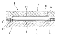
図1は、本発明に係る加速度センサの実施の形態1を示す断面図である。この加速度センサ2は、加速度センサ素子3を載置するためのベース部4と、ベース部4と接合してセンサ素子3を気密封止するためのキャップ部5とを備える。
Embodiment 1 FIG.
FIG. 1 is a cross-sectional view showing a first embodiment of an acceleration sensor according to the present invention. The
図2に上面図を示すベース部4は、矩形状のシリコン半導体基板6(広義には基板)を備え、該基板6の主面上には、加速度を検出するためのセンサ素子3と該センサ素子3を囲む枠部8とが設けてある。なお、枠部8は矩形状が一般的であるが、その形状は本発明を限定しない。加速度センサ素子3および枠部8は、例えば、半導体基板6上に、不純物としてリンがドーピングされたポリシリコン層を堆積した後、ポリシリコンをエッチングなどにより選択的に除去して形成される。ドーパントとして、リン以外に例えばガリウム、ボロン、ヒ素などでもよい。
2 includes a rectangular silicon semiconductor substrate 6 (substrate in a broad sense) and a
図3(a),(b)は、加速度センサ素子3を示す拡大図である。加速度センサ素子3は容量式の加速度センサ素子で、外力によって変位する重り部10を備える。重り部10は、半導体基板6主面と所定の間隔をあけて図3(a)左右方向を長手方向、上下方向を短手方向とした略矩形状の可動電極12を有する。可動電極12は、各短辺から長手方向にそれぞれ突出した突出部14L,14R、さらに短手方向に伸びた梁部16L,16Rを介して、半導体基板6主面上に固定された支持部18L,18Rに連結されている。梁部16L,16Rは、図3(a)上下方向長さに比べて左右方向長さ(幅)が短く左右方向に関して僅かに伸縮可能で、その結果、加速度センサ2が左右方向に外力を受けた場合に、可動電極12が左右方向に変位できるようになっている。可動電極12には、各長辺中央からそれぞれ短手方向に伸びた所定の大きさの溝20U,20Dが形成されている。各溝20U,20D内にはそれぞれ、半導体基板6主面上に固定された固定電極22U,22Dが配置されている。加速度センサ2が外力を受けて固定電極22Uと溝20Uを形成する可動電極12部分内面の隙間および固定電極22Dと溝20Dを形成する可動電極12部分内面の隙間が変化することで、可動電極12と各固定電極22U,22Dの間の静電容量が変化する(上述したように、可動電極12および固定電極22U,22Dを形成するポリシリコンには、電気的導通を図るためリンがドーピングされている。)。静電容量の変化は、電気信号として外部の容量計測回路(図示せず)に出力される。
3A and 3B are enlarged views showing the
加速度センサ素子3の構成は本発明を限定するものではなく、例えば可動電極が半導体基板6の主面方向に垂直な方向に変位できるものでもよい。また、容量式に限らず、ピエゾ抵抗式でもよい。
The configuration of the
図1,2に戻って、枠部8上にはノンドープのポリシリコン層24が形成されている。ポリシリコン層24は、例えばCVD法により成膜した例えばシリコン酸化膜で、枠部8を形成するポリシリコンに含まれるリンが拡散してポリシリコン層24とキャップ部5との接合界面に到達して析出することがないようにその厚みが設定されている。ポリシリコン層24は、枠部8とキャップ部5との間の中間層を構成する。枠部8とポリシリコン層24には、主面方向に関して略同一位置に枠状の貫通溝がそれぞれ形成され、全体として枠状の溝25を構成している。
1 and 2, a
キャップ部5は、シリコンの矩形状半導体基板から例えばザグリ加工により凹部26が形成されたキャップ(本体)27を備え、凹部26を形成する側の主面には金属層28が形成されている。金属層28は、キャップ27に、例えばチタン膜、続いてニッケル膜を例えば蒸着やスパッタリングで形成する。チタン膜とニッケル膜の厚さは、ポリシリコン層24との間の接合の強さおよび膜形成に伴って生じる残留応力を考慮して、それぞれ数十nm、数百nmが適当である。
The
加速度センサ2の製造時、ベース部4のポリシリコン層24とキャップ部5の金属層28を重ね合わせる。この状態で、真空下あるいは不活性ガス下の加熱炉内にベース部4およびキャップ部5を入れ、400℃で数十分から数時間加熱する。その結果、ポリシリコン層24のポリシリコンと金属層28のニッケルとが共晶合金を形成し、ベース部4とキャップ部5の接合が行われる。このとき、ベース部4のドーピングされた枠部8と金属層28の間にはノンドープのポリシリコン層24が介在されているので、枠部8を形成するポリシリコンに含まれるリンは、ノンドープのポリシリコン層24に拡散してもポリシリコン層4と金属層28との接合界面にリンが到達して析出することはない。その結果、ベース部4とキャップ部5の接合不良を防止できる。
When manufacturing the
かかる構成を備えた加速度センサ2は、ベース部4とキャップ部5との接合領域が多層構造となっているために、外力の影響を受けやすい。例えば、加速度センサ2を金属フレーム(図示せず)上に熱を加えてダイボンドする場合、シリコン半導体基板6と金属フレームの接着となるため両者の熱膨張係数の差から生じる残留応力、ダイボンド工程後に加速度センサ2等を封止するためのモールド工程時には、モールド樹脂を射出する圧力、加速度センサ2を搭載したデバイスの完成後には、加速度センサ2が置かれる環境(例えば熱履歴や湿気)によるモールドやダイボンドの劣化に伴う応力の変化などが外力として挙げられる。
The
溝25を有さない従来の構成では、上記外力により接合領域の各層間(半導体基板6と枠部8の間および枠部8とポリシリコン層24の間)でクラックが発生して、気密封止が破れ、加速度センサ素子3の特性が変動する場合がある。また、クラックに到らなくても、応力が枠部8や半導体基板6を通じて加速度センサ素子3まで伝播し、加速度センサ素子3の特性変動を引き起こす可能性がある。
In the conventional configuration having no
これに対し、本実施形態の構成では、外力によりクラックが生じた場合でも溝25でクラックの進行が止まるので、センサ2の気密性は保たれセンサ素子3の特性変動は生じない。応力もまた、溝25を超えて伝播しないので、センサ素子3の特性変動に影響を与えない。したがって、溝25を設けることで高信頼性の加速度センサ2を提供できる。
On the other hand, in the configuration of the present embodiment, even when a crack is generated by an external force, the progress of the crack is stopped in the
本実施形態ではまた、枠部8に設けた枠状の溝とポリシリコン層24に設けた枠状の溝は、互いに重なる位置に配設しているので、加速度センサ2の半導体基板6の主面方向に関する寸法の小型化を図ることができる。
In the present embodiment, the frame-shaped groove provided in the
実施の形態2.
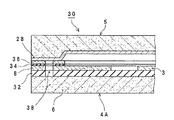
図4は、本発明に係る加速度センサの実施の形態2を示す部分拡大断面図である。以下の説明では、実施の形態1と同一または類似の構成要素は同一の符号または同一の符号に適当な添字を付して表す。
FIG. 4 is a partially enlarged sectional view showing a second embodiment of the acceleration sensor according to the present invention. In the following description, constituent elements that are the same as or similar to those in the first embodiment are represented by the same reference numerals or the same reference numerals with appropriate subscripts.
本実施形態に係る加速度センサ30において、半導体基板6の主面上には絶縁層32が形成されている。絶縁層32は、半導体基板6上に、例えばまずシリコン酸化膜、続いてシリコン窒化膜を例えばCVD法を用いて形成する。加速度センサ素子3と枠部8はこの絶縁層32上に形成され、これらの間が電気的に絶縁されている。
In the
金属層28と枠部8の間には、実施の形態1のように所定の厚みのポリシリコン層24を介在させる代わりに、拡散防止層としての絶縁層34およびノンドープのポリシリコン層36(これら層34、36が枠部8とキャップ部5の間の中間層を構成する。)を介在させる。このために、ベース部4Aの製造工程時、枠部8上に絶縁層34を例えばCVD法により、続いてポリシリコン層36を例えばスパッタリングにより形成する。次に、ベース部4Aのポリシリコン層36とキャップ部5の金属層28を重ね合わせる。この状態で、実施の形態1と同様にして、ポリシリコン層36のポリシリコンと金属層28のニッケルとが共晶合金を形成するように加熱し、ベース部4Aとキャップ部5の接合を行わせる。ポリシリコン層36と枠部8の間には拡散防止層34が介在されているので、枠部8を形成するシリコンに含まれるリンがノンドープのポリシリコン層36に拡散してポリシリコン層36と金属層28の界面に析出するのを防止できる。
Instead of interposing the
絶縁層32、枠部8、絶縁層34、およびポリシリコン層36には、主面方向に関して略同一位置に枠状の貫通溝がそれぞれ形成され、全体として枠状の溝38を構成している。
In the insulating
かかる構成を備えた加速度センサ30は、ベース部4Aとキャップ部5の接合領域が多層構造となっているために外力の影響を受けやすいが、外力によりクラックが生じた場合でも溝38でクラックの進行が止まるので、加速度センサ30の気密性は保たれ加速度センサ素子3の特性変動は生じない。応力もまた、溝38を超えて伝播しないので、加速度センサ素子3の特性変動に影響を与えない。したがって、溝38を設けることで高信頼性の加速度センサ30を提供できる。
The
本実施形態ではまた、絶縁層32、枠部8、絶縁層34、およびポリシリコン層36にそれぞれ設けた枠状の溝は、互いに重なる位置に配設しているので、加速度センサ30の半導体基板6の主面方向に関する寸法の小型化を図ることができる。
In the present embodiment, the frame-shaped grooves provided in the insulating
半導体基板6にも絶縁層32、枠部8、絶縁層34、およびポリシリコン層36と主面方向に関して略同一位置に枠状の溝を形成し、これにより、各層32,8,34,36とともに枠状の溝38を構成するようにしてもよい。溝38が半導体基板6まで至る構成は、応力の伝播距離が絶縁層32まで溝を設けた場合より長くなり、したがって上述の応力の伝播を防止する効果を増すことができるだけでなく、絶縁層32と半導体基板6との間で発生し得るクラックの進行および応力の伝播を防止する効果を有する。
A frame-like groove is also formed in the
実施の形態3.
図5は、本発明に係る加速度センサの実施の形態3を示す部分拡大断面図である。本実施形態に係る加速度センサ40は、実施の形態2の加速度センサ30の構成と類似しているが、ベース部4に溝38を設ける代わりに、キャップ本体27Bの接合領域に枠状の溝42を設ける。溝42は、凹部26Bと同一工程(例えばザグリ加工)で形成してもよいし、別工程(例えばエッチング)で形成してもよい。
FIG. 5 is a partially enlarged sectional view showing a third embodiment of the acceleration sensor according to the present invention. The
応力はキャップ部5B側を伝播する場合もあるが、本実施形態のように溝42を設けることで、応力は溝42を超えて伝播しないので、センサ素子3の特性変動に影響を与えず、したがって高信頼性の加速度センサ40を提供できる。
In some cases, the stress propagates on the
実施の形態4.
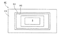
図6は、本発明に係る加速度センサの実施の形態4を示す断面図である。図7は、本実施形態に係る加速度センサ50のベース部4Cの上面図である。速度センサ50は、実施の形態1の加速度センサ2と類似の構成を有するが、ベース部とキャップ部との接合領域に溝25を設ける代わりに、接合領域よりも加速度センサ素子3側に延在した枠部8C部分(すなわち接合領域と加速度センサ素子3との間)に枠状の溝52を設けたものである。
FIG. 6 is a sectional view showing an acceleration sensor according to a fourth embodiment of the present invention. FIG. 7 is a top view of the
ベース部4Cとキャップ部5の接合においてポリシリコン層24と金属層28の材料(シリコンとニッケル)の熱膨張係数の差により生じる残留応力は、ポリシリコン層24と金属層28の接合端部54が最大となる。したがって、溝52を設けない場合、残留応力が枠部8C続いて半導体基板6を介して加速度センサ素子3に伝播し、該センサ素子3の特性変動が引き起こされる場合あるが、溝52を設けることで、応力は溝52を超えて伝播しないので、センサ素子3の特性変動に影響を与えず、したがって高信頼性の加速度センサ50を提供できる。
Residual stress caused by the difference in thermal expansion coefficient between the materials (silicon and nickel) of the
半導体基板6にも枠部8Cの枠状溝52と主面方向に関して略同一位置に枠状の溝を形成してもよい。
A frame-like groove may be formed in the
実施の形態5.
図8は、本発明に係る加速度センサの実施の形態5を示す断面図である。本実施形態に係る加速度センサ60は、実施の形態2の加速度センサ30と類似の構成を有するが、キャップ部とベース部との接合領域に溝38を設ける代わりに、接合領域よりも加速度センサ素子3側に延在した枠部8D部分および絶縁層32(すなわち接合領域と加速度センサ素子3との間)に枠状の溝62を設けたものである。
FIG. 8 is a sectional
キャップ部5の金属層28とベース部4Dのポリシリコン層36の接合においてニッケルとシリコンの熱膨張係数の差により生じる残留応力は、金属層28とポリシリコン層36の接合端部64が最大となる。したがって、溝62を設けない場合、残留応力がポリシリコン層36、絶縁層34、枠部8、絶縁層32、続いて半導体基板6を介して加速度センサ素子3に伝播し、該センサ素子3の特性変動が引き起こされる場合あるが、溝62を設けることで、応力は溝62を超えて伝播しないので、加速度センサ素子3の特性変動に影響を与えず、したがって高信頼性の加速度センサ60を提供できる。
Residual stress caused by the difference in thermal expansion coefficient between nickel and silicon in the joining of the
半導体基板6にも絶縁層32、枠部8Dと主面方向に関して略同一位置に枠状の溝を形成し、これにより、各層32,8Dとともに枠状の溝62を構成するようにしてもよい。
A frame-like groove may be formed in the
実施の形態6.
図9は、本発明に係る加速度センサの実施の形態6を示す断面図である。本実施形態に係る加速度センサ70は、実施の形態2,3,5と同様の溝38E,42E,62Eを備えたものである。ベース部4Eの溝38Eとキャップ部5Eの溝42Eは、半導体基板6の主面方向に関して略同一位置に形成され、加速度センサ70の主面方向に関する寸法の小型化が図られている。
FIG. 9 is a sectional
溝62Eを設ければ、溝38E,42Eを設けなくても加速度センサ素子3への応力の伝播は防止できるが、溝38E,42Eは主としてクラックによって加速度センサ70の気密封止が破れるのを防止するためのものである。
If the
以上、本発明の具体的な実施形態を説明したが、本発明はこれらに限らず種々改変可能である。例えば、枠部および枠部−キャップ部間に配置される中間層(例えば、実施の形態1であればポリシリコン層24であり、実施の形態2であれば少なくとも絶縁層34を含む層)にそれぞれ形成する枠状の溝は、半導体基板主面方向に関して略同一の位置に配設するのであれば、連通していない場合(中間層に形成する枠状溝が貫通溝でない場合)も本発明の範囲内に含まれる。但し、別工程で作製したベース部とキャップ部を接合する点や溝の形成のし易さの点などを考慮して、中間層に形成する溝は、中間層とキャップ部との接合界面に開放されているのが好ましい。また、ベース部とキャップ部との接合領域の各層間に発生し得るクラックや残留応力に対応するために、枠部および中間層の各溝は貫通溝であるのが好ましい。これは、溝の形成のし易さの点からも有利である。
Although specific embodiments of the present invention have been described above, the present invention is not limited to these and can be variously modified. For example, an intermediate layer (for example, a
さらに、実施の形態2,6において半導体基板に直に形成する絶縁層に溝を設けない構成も、本発明の範囲内に含まれる。 Furthermore, a configuration in which a groove is not provided in the insulating layer formed directly on the semiconductor substrate in the second and sixth embodiments is also included in the scope of the present invention.
加えて、中間層とキャップとの接合領域よりも内側に延在する部分に形成する枠状の溝は、貫通溝でない構成も本発明の範囲内に含まれる。 In addition, the frame-like groove formed in the portion extending inward from the joining region between the intermediate layer and the cap includes a configuration that is not a through groove.
3 加速度センサ素子
4A ベース部
5 キャップ部
6 半導体基板
8 枠部
28 金属層
30 加速度センサ
34 絶縁層
36 ノンドープのポリシリコン層
38 枠状の溝
DESCRIPTION OF
Claims (4)
基板上に配設された、加速度センサ素子および該センサ素子を囲む枠部と、
枠部上に配設された中間層と、
中間層と接合され、これにより加速度センサ素子を封止するキャップ部とを備え、
枠部および中間層にはそれぞれ、基板主面方向に関し略同一の位置に枠状の溝が設けてあることを特徴とする加速度センサ。 A substrate,
An acceleration sensor element disposed on the substrate and a frame portion surrounding the sensor element;
An intermediate layer disposed on the frame,
A cap portion that is bonded to the intermediate layer and thereby seals the acceleration sensor element;
An acceleration sensor characterized in that a frame-like groove is provided in each of the frame part and the intermediate layer at substantially the same position in the substrate main surface direction.
基板上に配設された、加速度センサ素子および該センサ素子を囲む枠部と、
枠部上に配設された中間層と、
中間層と接合され、これにより加速度センサ素子を封止するキャップ部とを備え、
枠部は、中間層とキャップ部との接合領域よりも加速度センサ素子側に延在する延在部を有し、該延在部に加速度センサ素子を囲むように枠状の溝が設けてあることを特徴とする加速度センサ。
A substrate,
An acceleration sensor element disposed on the substrate and a frame portion surrounding the sensor element;
An intermediate layer disposed on the frame,
A cap portion that is bonded to the intermediate layer and thereby seals the acceleration sensor element;
The frame portion has an extending portion that extends to the acceleration sensor element side with respect to the bonding region between the intermediate layer and the cap portion, and a frame-like groove is provided in the extending portion so as to surround the acceleration sensor element. An acceleration sensor characterized by that.
Priority Applications (6)
| Application Number | Priority Date | Filing Date | Title |
|---|---|---|---|
| JP2003311066A JP2005077349A (en) | 2003-09-03 | 2003-09-03 | Acceleration sensor |
| US10/816,812 US6988407B2 (en) | 2003-09-03 | 2004-04-05 | Acceleration sensor |
| TW093110193A TWI234659B (en) | 2003-09-03 | 2004-04-13 | Acceleration sensor |
| CNB2004100431437A CN100380129C (en) | 2003-09-03 | 2004-05-12 | Acceleration sensor |
| KR1020040043725A KR100555617B1 (en) | 2003-09-03 | 2004-06-14 | Acceleration sensor |
| DE102004028927A DE102004028927B4 (en) | 2003-09-03 | 2004-06-15 | accelerometer |
Applications Claiming Priority (1)
| Application Number | Priority Date | Filing Date | Title |
|---|---|---|---|
| JP2003311066A JP2005077349A (en) | 2003-09-03 | 2003-09-03 | Acceleration sensor |
Publications (2)
| Publication Number | Publication Date |
|---|---|
| JP2005077349A true JP2005077349A (en) | 2005-03-24 |
| JP2005077349A5 JP2005077349A5 (en) | 2006-03-09 |
Family
ID=34214245
Family Applications (1)
| Application Number | Title | Priority Date | Filing Date |
|---|---|---|---|
| JP2003311066A Pending JP2005077349A (en) | 2003-09-03 | 2003-09-03 | Acceleration sensor |
Country Status (6)
| Country | Link |
|---|---|
| US (1) | US6988407B2 (en) |
| JP (1) | JP2005077349A (en) |
| KR (1) | KR100555617B1 (en) |
| CN (1) | CN100380129C (en) |
| DE (1) | DE102004028927B4 (en) |
| TW (1) | TWI234659B (en) |
Cited By (6)
| Publication number | Priority date | Publication date | Assignee | Title |
|---|---|---|---|---|
| JP2009027055A (en) * | 2007-07-23 | 2009-02-05 | Seiko Instruments Inc | Airtight package, and method of manufacturing airtight package |
| JP2010139495A (en) * | 2008-11-13 | 2010-06-24 | Denso Corp | Semiconductor device and method for producing the same |
| JP2012127839A (en) * | 2010-12-16 | 2012-07-05 | Japan Aviation Electronics Industry Ltd | Capacitance type acceleration sensor |
| WO2012133765A1 (en) * | 2011-03-30 | 2012-10-04 | 株式会社村田製作所 | Bonding member for solid oxide fuel cell, solid oxide fuel cell, and solid oxide fuel cell module |
| JP2016135761A (en) * | 2015-01-14 | 2016-07-28 | 御木本製薬株式会社 | Defensin-production promotor, cathelicidin-production promotor, and antimicrobial agent |
| WO2018003353A1 (en) * | 2016-07-01 | 2018-01-04 | 株式会社デンソー | Semiconductor device |
Families Citing this family (8)
| Publication number | Priority date | Publication date | Assignee | Title |
|---|---|---|---|---|
| JP2006125887A (en) * | 2004-10-26 | 2006-05-18 | Fujitsu Media Device Kk | Acceleration sensor |
| US7406870B2 (en) * | 2005-01-06 | 2008-08-05 | Ricoh Company, Ltd. | Semiconductor sensor |
| JP4839747B2 (en) * | 2005-09-20 | 2011-12-21 | 三菱電機株式会社 | Capacitance type acceleration sensor |
| JP4486103B2 (en) * | 2007-03-19 | 2010-06-23 | Okiセミコンダクタ株式会社 | Acceleration sensor and method of manufacturing acceleration sensor |
| JP5446107B2 (en) * | 2008-03-17 | 2014-03-19 | 三菱電機株式会社 | Element wafer and method for manufacturing element wafer |
| CN103063876B (en) * | 2013-01-05 | 2014-08-20 | 中国科学院上海微系统与信息技术研究所 | Variable area type capacitive horizontal accelerated speed sensor and manufacture method |
| US10131540B2 (en) * | 2015-03-12 | 2018-11-20 | Taiwan Semiconductor Manufacturing Co., Ltd. | Structure and method to mitigate soldering offset for wafer-level chip scale package (WLCSP) applications |
| JP6729423B2 (en) | 2017-01-27 | 2020-07-22 | 三菱電機株式会社 | Semiconductor device and method of manufacturing semiconductor device |
Family Cites Families (7)
| Publication number | Priority date | Publication date | Assignee | Title |
|---|---|---|---|---|
| FI81915C (en) * | 1987-11-09 | 1990-12-10 | Vaisala Oy | KAPACITIV ACCELERATIONSGIVARE OCH FOERFARANDE FOER FRAMSTAELLNING DAERAV. |
| US5121180A (en) * | 1991-06-21 | 1992-06-09 | Texas Instruments Incorporated | Accelerometer with central mass in support |
| JP2000022169A (en) * | 1998-06-29 | 2000-01-21 | Matsushita Electric Works Ltd | Semiconductor acceleration sensor and manufacture thereof |
| JP2000187040A (en) | 1998-12-22 | 2000-07-04 | Matsushita Electric Works Ltd | Acceleration sensor and its manufacture |
| JP2001337103A (en) | 2000-05-26 | 2001-12-07 | Matsushita Electric Works Ltd | Semiconductor acceleration sensor |
| JP4386559B2 (en) | 2000-10-20 | 2009-12-16 | 三菱電機株式会社 | Acceleration sensor and manufacturing method thereof |
| JP4156946B2 (en) * | 2003-02-26 | 2008-09-24 | 三菱電機株式会社 | Acceleration sensor |
-
2003
- 2003-09-03 JP JP2003311066A patent/JP2005077349A/en active Pending
-
2004
- 2004-04-05 US US10/816,812 patent/US6988407B2/en not_active Expired - Fee Related
- 2004-04-13 TW TW093110193A patent/TWI234659B/en not_active IP Right Cessation
- 2004-05-12 CN CNB2004100431437A patent/CN100380129C/en not_active Expired - Fee Related
- 2004-06-14 KR KR1020040043725A patent/KR100555617B1/en not_active IP Right Cessation
- 2004-06-15 DE DE102004028927A patent/DE102004028927B4/en not_active Expired - Fee Related
Cited By (7)
| Publication number | Priority date | Publication date | Assignee | Title |
|---|---|---|---|---|
| JP2009027055A (en) * | 2007-07-23 | 2009-02-05 | Seiko Instruments Inc | Airtight package, and method of manufacturing airtight package |
| JP2010139495A (en) * | 2008-11-13 | 2010-06-24 | Denso Corp | Semiconductor device and method for producing the same |
| JP2012127839A (en) * | 2010-12-16 | 2012-07-05 | Japan Aviation Electronics Industry Ltd | Capacitance type acceleration sensor |
| WO2012133765A1 (en) * | 2011-03-30 | 2012-10-04 | 株式会社村田製作所 | Bonding member for solid oxide fuel cell, solid oxide fuel cell, and solid oxide fuel cell module |
| WO2012133087A1 (en) * | 2011-03-30 | 2012-10-04 | 株式会社村田製作所 | Bonding member for solid oxide fuel cell, solid oxide fuel cell, and solid oxide fuel cell module |
| JP2016135761A (en) * | 2015-01-14 | 2016-07-28 | 御木本製薬株式会社 | Defensin-production promotor, cathelicidin-production promotor, and antimicrobial agent |
| WO2018003353A1 (en) * | 2016-07-01 | 2018-01-04 | 株式会社デンソー | Semiconductor device |
Also Published As
| Publication number | Publication date |
|---|---|
| KR100555617B1 (en) | 2006-03-03 |
| US20050044953A1 (en) | 2005-03-03 |
| TWI234659B (en) | 2005-06-21 |
| DE102004028927A1 (en) | 2005-04-07 |
| CN100380129C (en) | 2008-04-09 |
| US6988407B2 (en) | 2006-01-24 |
| TW200510727A (en) | 2005-03-16 |
| DE102004028927B4 (en) | 2008-07-24 |
| KR20050025224A (en) | 2005-03-14 |
| CN1591023A (en) | 2005-03-09 |
Similar Documents
| Publication | Publication Date | Title |
|---|---|---|
| US8497557B2 (en) | Semiconductor device | |
| US6789423B2 (en) | Micro inertia sensor and method of manufacturing the same | |
| JP2005077349A (en) | Acceleration sensor | |
| EP1074827B1 (en) | Pressure sensor and method of manufacturing the same | |
| JP4495711B2 (en) | Functional element and manufacturing method thereof | |
| US7762141B2 (en) | Pressure sensor and manufacturing method thereof | |
| US9000544B2 (en) | MEMS package structure | |
| JP2004170390A (en) | Sensor for dynamic quantity | |
| JP2003337075A (en) | Absolute pressure type pressure sensor | |
| JP2001326367A (en) | Sensor and method for manufacturing the same | |
| JP2005172543A (en) | Acceleration sensor and manufacturing method therefor | |
| JP2009014469A (en) | Semiconductor device and method for manufacturing the same | |
| JP7233982B2 (en) | Package and package manufacturing method | |
| JP5727798B2 (en) | MEMS sensor | |
| KR100311826B1 (en) | Method for hermetic packaging in microsensors | |
| JP7079075B2 (en) | package | |
| JP2002134759A (en) | Acceleration sensor and manufacturing method therefor | |
| JP2007057455A (en) | Pressure sensor and manufacturing method thereof | |
| JPH0831609B2 (en) | Electrostatic bonding method and semiconductor pressure sensor | |
| JP2005223209A (en) | Vacuum package sensor element, wafer level vacuum package, and manufacturing method thereof | |
| JP4095280B2 (en) | Acceleration sensor element | |
| JP2007292658A (en) | Pressure sensor and manufacturing method of same | |
| JP2004132811A (en) | Force detecting element, and manufacturing method of force detecting element | |
| JP2007078444A (en) | Pressure sensor and manufacturing method for pressure sensor | |
| JPH10107295A (en) | Semiconductor sensor |
Legal Events
| Date | Code | Title | Description |
|---|---|---|---|
| A521 | Written amendment |
Free format text: JAPANESE INTERMEDIATE CODE: A523 Effective date: 20060118 |
|
| A621 | Written request for application examination |
Free format text: JAPANESE INTERMEDIATE CODE: A621 Effective date: 20060118 |
|
| A977 | Report on retrieval |
Free format text: JAPANESE INTERMEDIATE CODE: A971007 Effective date: 20080728 |
|
| A131 | Notification of reasons for refusal |
Free format text: JAPANESE INTERMEDIATE CODE: A131 Effective date: 20080902 |
|
| A521 | Written amendment |
Free format text: JAPANESE INTERMEDIATE CODE: A523 Effective date: 20081029 |
|
| RD03 | Notification of appointment of power of attorney |
Free format text: JAPANESE INTERMEDIATE CODE: A7423 Effective date: 20081029 |
|
| A02 | Decision of refusal |
Free format text: JAPANESE INTERMEDIATE CODE: A02 Effective date: 20081125 |