JP2005057260A - Thin-film transistor circuit device, method for manufacturing the same, and liquid crystal display device using the same - Google Patents
Thin-film transistor circuit device, method for manufacturing the same, and liquid crystal display device using the same Download PDFInfo
- Publication number
- JP2005057260A JP2005057260A JP2004212977A JP2004212977A JP2005057260A JP 2005057260 A JP2005057260 A JP 2005057260A JP 2004212977 A JP2004212977 A JP 2004212977A JP 2004212977 A JP2004212977 A JP 2004212977A JP 2005057260 A JP2005057260 A JP 2005057260A
- Authority
- JP
- Japan
- Prior art keywords
- film transistor
- thin film
- circuit device
- wiring
- transistor circuit
- Prior art date
- Legal status (The legal status is an assumption and is not a legal conclusion. Google has not performed a legal analysis and makes no representation as to the accuracy of the status listed.)
- Pending
Links
- 239000010409 thin film Substances 0.000 title claims abstract description 200
- 238000004519 manufacturing process Methods 0.000 title claims abstract description 41
- 239000004973 liquid crystal related substance Substances 0.000 title claims description 25
- 238000000034 method Methods 0.000 title abstract description 67
- 229910001182 Mo alloy Inorganic materials 0.000 claims abstract description 108
- 239000010955 niobium Substances 0.000 claims abstract description 101
- 229910052758 niobium Inorganic materials 0.000 claims abstract description 99
- GUCVJGMIXFAOAE-UHFFFAOYSA-N niobium atom Chemical compound [Nb] GUCVJGMIXFAOAE-UHFFFAOYSA-N 0.000 claims abstract description 98
- 229910052750 molybdenum Inorganic materials 0.000 claims abstract description 55
- ZOKXTWBITQBERF-UHFFFAOYSA-N Molybdenum Chemical compound [Mo] ZOKXTWBITQBERF-UHFFFAOYSA-N 0.000 claims abstract description 54
- 239000011733 molybdenum Substances 0.000 claims abstract description 54
- 229910000838 Al alloy Inorganic materials 0.000 claims abstract description 36
- 229910052782 aluminium Inorganic materials 0.000 claims abstract description 36
- XAGFODPZIPBFFR-UHFFFAOYSA-N aluminium Chemical compound [Al] XAGFODPZIPBFFR-UHFFFAOYSA-N 0.000 claims abstract description 36
- 239000012298 atmosphere Substances 0.000 claims abstract description 13
- 239000010408 film Substances 0.000 claims description 188
- 239000000758 substrate Substances 0.000 claims description 55
- 229910052751 metal Inorganic materials 0.000 claims description 49
- 239000002184 metal Substances 0.000 claims description 49
- 229910052779 Neodymium Inorganic materials 0.000 claims description 24
- QEFYFXOXNSNQGX-UHFFFAOYSA-N neodymium atom Chemical compound [Nd] QEFYFXOXNSNQGX-UHFFFAOYSA-N 0.000 claims description 24
- 230000015572 biosynthetic process Effects 0.000 claims description 14
- QVGXLLKOCUKJST-UHFFFAOYSA-N atomic oxygen Chemical compound [O] QVGXLLKOCUKJST-UHFFFAOYSA-N 0.000 claims description 10
- 229910000484 niobium oxide Inorganic materials 0.000 claims description 10
- URLJKFSTXLNXLG-UHFFFAOYSA-N niobium(5+);oxygen(2-) Chemical compound [O-2].[O-2].[O-2].[O-2].[O-2].[Nb+5].[Nb+5] URLJKFSTXLNXLG-UHFFFAOYSA-N 0.000 claims description 10
- 239000001301 oxygen Substances 0.000 claims description 10
- 229910052760 oxygen Inorganic materials 0.000 claims description 10
- RYGMFSIKBFXOCR-UHFFFAOYSA-N Copper Chemical compound [Cu] RYGMFSIKBFXOCR-UHFFFAOYSA-N 0.000 claims description 7
- XUIMIQQOPSSXEZ-UHFFFAOYSA-N Silicon Chemical compound [Si] XUIMIQQOPSSXEZ-UHFFFAOYSA-N 0.000 claims description 7
- 229910052802 copper Inorganic materials 0.000 claims description 7
- 239000010949 copper Substances 0.000 claims description 7
- 229910052710 silicon Inorganic materials 0.000 claims description 7
- 239000010703 silicon Substances 0.000 claims description 7
- 229910052709 silver Inorganic materials 0.000 claims description 7
- 239000004332 silver Substances 0.000 claims description 7
- 230000003647 oxidation Effects 0.000 claims description 4
- 238000007254 oxidation reaction Methods 0.000 claims description 4
- AMGQUBHHOARCQH-UHFFFAOYSA-N indium;oxotin Chemical compound [In].[Sn]=O AMGQUBHHOARCQH-UHFFFAOYSA-N 0.000 claims description 2
- 230000001590 oxidative effect Effects 0.000 claims description 2
- YVTHLONGBIQYBO-UHFFFAOYSA-N zinc indium(3+) oxygen(2-) Chemical compound [O--].[Zn++].[In+3] YVTHLONGBIQYBO-UHFFFAOYSA-N 0.000 claims description 2
- TYHJXGDMRRJCRY-UHFFFAOYSA-N zinc indium(3+) oxygen(2-) tin(4+) Chemical compound [O-2].[Zn+2].[Sn+4].[In+3] TYHJXGDMRRJCRY-UHFFFAOYSA-N 0.000 claims description 2
- 229910045601 alloy Inorganic materials 0.000 abstract description 36
- 239000000956 alloy Substances 0.000 abstract description 36
- 230000007797 corrosion Effects 0.000 abstract description 13
- 238000005260 corrosion Methods 0.000 abstract description 13
- 239000010410 layer Substances 0.000 description 87
- 238000005530 etching Methods 0.000 description 37
- 229910021417 amorphous silicon Inorganic materials 0.000 description 35
- 238000000206 photolithography Methods 0.000 description 32
- QTBSBXVTEAMEQO-UHFFFAOYSA-N Acetic acid Chemical compound CC(O)=O QTBSBXVTEAMEQO-UHFFFAOYSA-N 0.000 description 31
- NBIIXXVUZAFLBC-UHFFFAOYSA-N Phosphoric acid Chemical compound OP(O)(O)=O NBIIXXVUZAFLBC-UHFFFAOYSA-N 0.000 description 20
- 150000004767 nitrides Chemical class 0.000 description 19
- 230000001681 protective effect Effects 0.000 description 16
- 238000001312 dry etching Methods 0.000 description 13
- 238000001039 wet etching Methods 0.000 description 13
- GRYLNZFGIOXLOG-UHFFFAOYSA-N Nitric acid Chemical compound O[N+]([O-])=O GRYLNZFGIOXLOG-UHFFFAOYSA-N 0.000 description 11
- 239000011521 glass Substances 0.000 description 11
- 229910017604 nitric acid Inorganic materials 0.000 description 11
- 238000004544 sputter deposition Methods 0.000 description 11
- XKRFYHLGVUSROY-UHFFFAOYSA-N Argon Chemical compound [Ar] XKRFYHLGVUSROY-UHFFFAOYSA-N 0.000 description 10
- 229910000147 aluminium phosphate Inorganic materials 0.000 description 10
- 239000011651 chromium Substances 0.000 description 9
- 229910052804 chromium Inorganic materials 0.000 description 8
- 239000000463 material Substances 0.000 description 7
- VYZAMTAEIAYCRO-UHFFFAOYSA-N Chromium Chemical compound [Cr] VYZAMTAEIAYCRO-UHFFFAOYSA-N 0.000 description 6
- 229920002120 photoresistant polymer Polymers 0.000 description 6
- 239000000243 solution Substances 0.000 description 6
- BQCADISMDOOEFD-UHFFFAOYSA-N Silver Chemical compound [Ag] BQCADISMDOOEFD-UHFFFAOYSA-N 0.000 description 5
- 229910052786 argon Inorganic materials 0.000 description 5
- 239000004065 semiconductor Substances 0.000 description 5
- 238000010586 diagram Methods 0.000 description 4
- 239000003870 refractory metal Substances 0.000 description 4
- 239000003513 alkali Substances 0.000 description 3
- 238000004380 ashing Methods 0.000 description 3
- 229910021420 polycrystalline silicon Inorganic materials 0.000 description 3
- 238000006243 chemical reaction Methods 0.000 description 2
- -1 composed of silver Chemical compound 0.000 description 2
- 230000000694 effects Effects 0.000 description 2
- 230000005684 electric field Effects 0.000 description 2
- 230000005496 eutectics Effects 0.000 description 2
- 229910052735 hafnium Inorganic materials 0.000 description 2
- 229920005591 polysilicon Polymers 0.000 description 2
- 229910052715 tantalum Inorganic materials 0.000 description 2
- 229910052719 titanium Inorganic materials 0.000 description 2
- 229910052721 tungsten Inorganic materials 0.000 description 2
- 229910052720 vanadium Inorganic materials 0.000 description 2
- 229910052726 zirconium Inorganic materials 0.000 description 2
- 229910021364 Al-Si alloy Inorganic materials 0.000 description 1
- 229910001257 Nb alloy Inorganic materials 0.000 description 1
- 229910000583 Nd alloy Inorganic materials 0.000 description 1
- VYPSYNLAJGMNEJ-UHFFFAOYSA-N Silicium dioxide Chemical compound O=[Si]=O VYPSYNLAJGMNEJ-UHFFFAOYSA-N 0.000 description 1
- UBSJOWMHLJZVDJ-UHFFFAOYSA-N aluminum neodymium Chemical compound [Al].[Nd] UBSJOWMHLJZVDJ-UHFFFAOYSA-N 0.000 description 1
- 239000012300 argon atmosphere Substances 0.000 description 1
- 230000004888 barrier function Effects 0.000 description 1
- XMPZTFVPEKAKFH-UHFFFAOYSA-P ceric ammonium nitrate Chemical compound [NH4+].[NH4+].[Ce+4].[O-][N+]([O-])=O.[O-][N+]([O-])=O.[O-][N+]([O-])=O.[O-][N+]([O-])=O.[O-][N+]([O-])=O.[O-][N+]([O-])=O XMPZTFVPEKAKFH-UHFFFAOYSA-P 0.000 description 1
- 239000007789 gas Substances 0.000 description 1
- 238000010438 heat treatment Methods 0.000 description 1
- 239000001307 helium Substances 0.000 description 1
- 229910052734 helium Inorganic materials 0.000 description 1
- SWQJXJOGLNCZEY-UHFFFAOYSA-N helium atom Chemical compound [He] SWQJXJOGLNCZEY-UHFFFAOYSA-N 0.000 description 1
- 239000012535 impurity Substances 0.000 description 1
- 239000011261 inert gas Substances 0.000 description 1
- 239000011229 interlayer Substances 0.000 description 1
- 238000010030 laminating Methods 0.000 description 1
- 230000008018 melting Effects 0.000 description 1
- 238000002844 melting Methods 0.000 description 1
- 239000011259 mixed solution Substances 0.000 description 1
- 229910021421 monocrystalline silicon Inorganic materials 0.000 description 1
- 230000002093 peripheral effect Effects 0.000 description 1
- 239000002356 single layer Substances 0.000 description 1
Images


Classifications
-
- G—PHYSICS
- G02—OPTICS
- G02F—OPTICAL DEVICES OR ARRANGEMENTS FOR THE CONTROL OF LIGHT BY MODIFICATION OF THE OPTICAL PROPERTIES OF THE MEDIA OF THE ELEMENTS INVOLVED THEREIN; NON-LINEAR OPTICS; FREQUENCY-CHANGING OF LIGHT; OPTICAL LOGIC ELEMENTS; OPTICAL ANALOGUE/DIGITAL CONVERTERS
- G02F1/00—Devices or arrangements for the control of the intensity, colour, phase, polarisation or direction of light arriving from an independent light source, e.g. switching, gating or modulating; Non-linear optics
- G02F1/01—Devices or arrangements for the control of the intensity, colour, phase, polarisation or direction of light arriving from an independent light source, e.g. switching, gating or modulating; Non-linear optics for the control of the intensity, phase, polarisation or colour
- G02F1/13—Devices or arrangements for the control of the intensity, colour, phase, polarisation or direction of light arriving from an independent light source, e.g. switching, gating or modulating; Non-linear optics for the control of the intensity, phase, polarisation or colour based on liquid crystals, e.g. single liquid crystal display cells
- G02F1/133—Constructional arrangements; Operation of liquid crystal cells; Circuit arrangements
- G02F1/1333—Constructional arrangements; Manufacturing methods
- G02F1/1345—Conductors connecting electrodes to cell terminals
- G02F1/13458—Terminal pads
-
- G—PHYSICS
- G02—OPTICS
- G02F—OPTICAL DEVICES OR ARRANGEMENTS FOR THE CONTROL OF LIGHT BY MODIFICATION OF THE OPTICAL PROPERTIES OF THE MEDIA OF THE ELEMENTS INVOLVED THEREIN; NON-LINEAR OPTICS; FREQUENCY-CHANGING OF LIGHT; OPTICAL LOGIC ELEMENTS; OPTICAL ANALOGUE/DIGITAL CONVERTERS
- G02F1/00—Devices or arrangements for the control of the intensity, colour, phase, polarisation or direction of light arriving from an independent light source, e.g. switching, gating or modulating; Non-linear optics
- G02F1/01—Devices or arrangements for the control of the intensity, colour, phase, polarisation or direction of light arriving from an independent light source, e.g. switching, gating or modulating; Non-linear optics for the control of the intensity, phase, polarisation or colour
- G02F1/13—Devices or arrangements for the control of the intensity, colour, phase, polarisation or direction of light arriving from an independent light source, e.g. switching, gating or modulating; Non-linear optics for the control of the intensity, phase, polarisation or colour based on liquid crystals, e.g. single liquid crystal display cells
- G02F1/133—Constructional arrangements; Operation of liquid crystal cells; Circuit arrangements
- G02F1/136—Liquid crystal cells structurally associated with a semi-conducting layer or substrate, e.g. cells forming part of an integrated circuit
- G02F1/1362—Active matrix addressed cells
- G02F1/136286—Wiring, e.g. gate line, drain line
- G02F1/13629—Multilayer wirings
-
- H—ELECTRICITY
- H01—ELECTRIC ELEMENTS
- H01L—SEMICONDUCTOR DEVICES NOT COVERED BY CLASS H10
- H01L27/00—Devices consisting of a plurality of semiconductor or other solid-state components formed in or on a common substrate
- H01L27/02—Devices consisting of a plurality of semiconductor or other solid-state components formed in or on a common substrate including semiconductor components specially adapted for rectifying, oscillating, amplifying or switching and having at least one potential-jump barrier or surface barrier; including integrated passive circuit elements with at least one potential-jump barrier or surface barrier
- H01L27/12—Devices consisting of a plurality of semiconductor or other solid-state components formed in or on a common substrate including semiconductor components specially adapted for rectifying, oscillating, amplifying or switching and having at least one potential-jump barrier or surface barrier; including integrated passive circuit elements with at least one potential-jump barrier or surface barrier the substrate being other than a semiconductor body, e.g. an insulating body
- H01L27/1214—Devices consisting of a plurality of semiconductor or other solid-state components formed in or on a common substrate including semiconductor components specially adapted for rectifying, oscillating, amplifying or switching and having at least one potential-jump barrier or surface barrier; including integrated passive circuit elements with at least one potential-jump barrier or surface barrier the substrate being other than a semiconductor body, e.g. an insulating body comprising a plurality of TFTs formed on a non-semiconducting substrate, e.g. driving circuits for AMLCDs
- H01L27/124—Devices consisting of a plurality of semiconductor or other solid-state components formed in or on a common substrate including semiconductor components specially adapted for rectifying, oscillating, amplifying or switching and having at least one potential-jump barrier or surface barrier; including integrated passive circuit elements with at least one potential-jump barrier or surface barrier the substrate being other than a semiconductor body, e.g. an insulating body comprising a plurality of TFTs formed on a non-semiconducting substrate, e.g. driving circuits for AMLCDs with a particular composition, shape or layout of the wiring layers specially adapted to the circuit arrangement, e.g. scanning lines in LCD pixel circuits
-
- H—ELECTRICITY
- H01—ELECTRIC ELEMENTS
- H01L—SEMICONDUCTOR DEVICES NOT COVERED BY CLASS H10
- H01L29/00—Semiconductor devices adapted for rectifying, amplifying, oscillating or switching, or capacitors or resistors with at least one potential-jump barrier or surface barrier, e.g. PN junction depletion layer or carrier concentration layer; Details of semiconductor bodies or of electrodes thereof ; Multistep manufacturing processes therefor
- H01L29/40—Electrodes ; Multistep manufacturing processes therefor
- H01L29/43—Electrodes ; Multistep manufacturing processes therefor characterised by the materials of which they are formed
- H01L29/45—Ohmic electrodes
- H01L29/456—Ohmic electrodes on silicon
-
- H—ELECTRICITY
- H01—ELECTRIC ELEMENTS
- H01L—SEMICONDUCTOR DEVICES NOT COVERED BY CLASS H10
- H01L29/00—Semiconductor devices adapted for rectifying, amplifying, oscillating or switching, or capacitors or resistors with at least one potential-jump barrier or surface barrier, e.g. PN junction depletion layer or carrier concentration layer; Details of semiconductor bodies or of electrodes thereof ; Multistep manufacturing processes therefor
- H01L29/40—Electrodes ; Multistep manufacturing processes therefor
- H01L29/43—Electrodes ; Multistep manufacturing processes therefor characterised by the materials of which they are formed
- H01L29/49—Metal-insulator-semiconductor electrodes, e.g. gates of MOSFET
- H01L29/4908—Metal-insulator-semiconductor electrodes, e.g. gates of MOSFET for thin film semiconductor, e.g. gate of TFT
-
- H—ELECTRICITY
- H01—ELECTRIC ELEMENTS
- H01L—SEMICONDUCTOR DEVICES NOT COVERED BY CLASS H10
- H01L29/00—Semiconductor devices adapted for rectifying, amplifying, oscillating or switching, or capacitors or resistors with at least one potential-jump barrier or surface barrier, e.g. PN junction depletion layer or carrier concentration layer; Details of semiconductor bodies or of electrodes thereof ; Multistep manufacturing processes therefor
- H01L29/66—Types of semiconductor device ; Multistep manufacturing processes therefor
- H01L29/66007—Multistep manufacturing processes
- H01L29/66075—Multistep manufacturing processes of devices having semiconductor bodies comprising group 14 or group 13/15 materials
- H01L29/66227—Multistep manufacturing processes of devices having semiconductor bodies comprising group 14 or group 13/15 materials the devices being controllable only by the electric current supplied or the electric potential applied, to an electrode which does not carry the current to be rectified, amplified or switched, e.g. three-terminal devices
- H01L29/66409—Unipolar field-effect transistors
- H01L29/66477—Unipolar field-effect transistors with an insulated gate, i.e. MISFET
- H01L29/66742—Thin film unipolar transistors
- H01L29/6675—Amorphous silicon or polysilicon transistors
- H01L29/66765—Lateral single gate single channel transistors with inverted structure, i.e. the channel layer is formed after the gate
-
- H—ELECTRICITY
- H01—ELECTRIC ELEMENTS
- H01L—SEMICONDUCTOR DEVICES NOT COVERED BY CLASS H10
- H01L29/00—Semiconductor devices adapted for rectifying, amplifying, oscillating or switching, or capacitors or resistors with at least one potential-jump barrier or surface barrier, e.g. PN junction depletion layer or carrier concentration layer; Details of semiconductor bodies or of electrodes thereof ; Multistep manufacturing processes therefor
- H01L29/66—Types of semiconductor device ; Multistep manufacturing processes therefor
- H01L29/68—Types of semiconductor device ; Multistep manufacturing processes therefor controllable by only the electric current supplied, or only the electric potential applied, to an electrode which does not carry the current to be rectified, amplified or switched
- H01L29/76—Unipolar devices, e.g. field effect transistors
- H01L29/772—Field effect transistors
- H01L29/78—Field effect transistors with field effect produced by an insulated gate
- H01L29/786—Thin film transistors, i.e. transistors with a channel being at least partly a thin film
- H01L29/78651—Silicon transistors
- H01L29/7866—Non-monocrystalline silicon transistors
- H01L29/78663—Amorphous silicon transistors
- H01L29/78669—Amorphous silicon transistors with inverted-type structure, e.g. with bottom gate
-
- H—ELECTRICITY
- H01—ELECTRIC ELEMENTS
- H01L—SEMICONDUCTOR DEVICES NOT COVERED BY CLASS H10
- H01L29/00—Semiconductor devices adapted for rectifying, amplifying, oscillating or switching, or capacitors or resistors with at least one potential-jump barrier or surface barrier, e.g. PN junction depletion layer or carrier concentration layer; Details of semiconductor bodies or of electrodes thereof ; Multistep manufacturing processes therefor
- H01L29/66—Types of semiconductor device ; Multistep manufacturing processes therefor
- H01L29/68—Types of semiconductor device ; Multistep manufacturing processes therefor controllable by only the electric current supplied, or only the electric potential applied, to an electrode which does not carry the current to be rectified, amplified or switched
- H01L29/76—Unipolar devices, e.g. field effect transistors
- H01L29/772—Field effect transistors
- H01L29/78—Field effect transistors with field effect produced by an insulated gate
- H01L29/786—Thin film transistors, i.e. transistors with a channel being at least partly a thin film
- H01L29/78651—Silicon transistors
- H01L29/7866—Non-monocrystalline silicon transistors
- H01L29/78672—Polycrystalline or microcrystalline silicon transistor
- H01L29/78678—Polycrystalline or microcrystalline silicon transistor with inverted-type structure, e.g. with bottom gate
Abstract
Description
本発明は、薄膜トランジスタ回路装置およびその製造方法および薄膜トランジスタ回路装置を用いた液晶表示装置に関するものである。 The present invention relates to a thin film transistor circuit device, a manufacturing method thereof, and a liquid crystal display device using the thin film transistor circuit device.
近年、液晶表示装置は、薄膜トランジスタ(TFT(Thin Film Transistor))液晶表示装置が主流となり、薄膜トランジスタは、薄膜トランジスタ液晶表示層の大型化、微細化に伴い改良が加えられてきた。最近では更に、薄膜トランジスタが、液晶表示装置の画素を駆動するスイッチング素子として以外に液晶表示装置を駆動するドライバー回路や静電保護回路用のトランジスタとして薄膜トランジスタ回路装置に作りこまれることが行われるようになってきている。 In recent years, thin film transistor (TFT) liquid crystal display devices have become the mainstream of liquid crystal display devices, and thin film transistors have been improved as the thin film transistor liquid crystal display layers become larger and finer. Recently, a thin film transistor has been incorporated into a thin film transistor circuit device as a driver circuit for driving a liquid crystal display device or a transistor for an electrostatic protection circuit in addition to a switching element for driving a pixel of the liquid crystal display device. It has become to.
このために、薄膜トランジスタ回路装置のトランジスタ間の接続に用いられる配線に対する要求も厳しくなってきている。 For this reason, the requirement for wiring used for connection between transistors of the thin film transistor circuit device has also become strict.
従来、薄膜トランジスタ回路装置に形成される配線には配線抵抗を減らすためにアルミニウムまたはアルミニウム合金のようなアルミニウム系配線が用いられてきた。 Conventionally, aluminum wiring such as aluminum or aluminum alloy has been used for wiring formed in a thin film transistor circuit device in order to reduce wiring resistance.
しかしながらアルミニウム系配線は、熱履歴によりヒロックが生じ易いという欠点がある。ヒロックは先端がとがった形状をしているため、対向する基板を傷つける等の問題を発生する場合がある。この欠点を改善するため、アルミニウム系配線の上に高融点金属膜を積層する積層配線がある。特開平11−259016号公報に、アルミニウム系配線のヒロックを防止するため、アルミニウム系の配線上に高融点金属(例えばモリブデン)膜を積層させる技術が開示されている。 However, aluminum-based wiring has a drawback that hillocks are likely to occur due to thermal history. Since the hillock has a sharp pointed shape, it may cause problems such as damage to the opposing substrate. In order to improve this drawback, there is a laminated wiring in which a refractory metal film is laminated on an aluminum-based wiring. Japanese Patent Application Laid-Open No. 11-259016 discloses a technique of laminating a refractory metal (for example, molybdenum) film on an aluminum-based wiring in order to prevent hillocks in the aluminum-based wiring.
特開平11−259016号公報によれば、ネオジム(Nd)を含むアルミニウム合金を下層に、上層に高融点金属を用いた積層配線が開示されている。特許文献1では、高融点金属として、Cr、Mo、W、Ti、Zr、Hf、V、Nb、Taから選ばれた一の金属またはそれらの合金が開示されている。
Japanese Patent Application Laid-Open No. 11-259016 discloses a multilayer wiring using an aluminum alloy containing neodymium (Nd) as a lower layer and a refractory metal as an upper layer.
これに対し、端子を露出するために窒化膜をドライエッチングでエッチング除去する際、モリブデン系合金がエッチングされることを防止するために、特開2000−284326号公報には、モリブデン(Mo)にニオブ(Nb)を約17原子%以上添加することで、ニオブを含むモリブデン合金のエッチングレートを窒化膜のエッチングレートの4分の1以下とすることができることが開示されている。
しかしながら、上述のモリブデン系の配線は、大気中の水分により腐食が進行し易いという性質を有する。従ってモリブデン系の配線は、表面が大気中に露出している端子部においてモリブデン腐食を生じ易く、外部との接続信頼性が良くない。また、高融点金属としてモリブデン以外のCr、W、Ti、Zr、Hf、V、Nb、Taを適用した場合、アルミニウム合金に積層させた形でのウェットエッチングが困難であり、ゲート配線側面のテーパ形状が悪くなり、ゲート配線の上層に層間絶縁膜を挟んで形成されるドレインおよびソース配線の断線が生じ易くなる。 However, the molybdenum-based wiring described above has a property that corrosion easily proceeds due to moisture in the atmosphere. Therefore, molybdenum-based wiring is liable to cause molybdenum corrosion at the terminal portion whose surface is exposed to the atmosphere, and the connection reliability with the outside is not good. In addition, when Cr, W, Ti, Zr, Hf, V, Nb, Ta other than molybdenum is applied as the refractory metal, wet etching in a form laminated on an aluminum alloy is difficult, and the taper on the side surface of the gate wiring is difficult. The shape deteriorates, and disconnection of the drain and source wirings formed with the interlayer insulating film sandwiched between the gate wirings is likely to occur.
また、特開2000−284326号公報によれば、配線を覆う窒化膜と配線の上層を構成するモリブデン系合金とのドライエッチングの選択比を上げるためにモリブデンにニオブを約17原子%以上添加すると、ニオブを含むモリブデン合金のエッチングレートを窒化膜のエッチングレートの4分の1以下とすることができて好ましいとしている。しかしながら、ニオブを含むモリブデン合金の耐腐食性については何の知見も開示していない。 According to Japanese Patent Laid-Open No. 2000-284326, when niobium is added to molybdenum at about 17 atomic% or more in order to increase the dry etching selectivity between the nitride film covering the wiring and the molybdenum-based alloy constituting the upper layer of the wiring. The etching rate of the molybdenum alloy containing niobium can be reduced to a quarter or less of the etching rate of the nitride film. However, no knowledge is disclosed about the corrosion resistance of molybdenum alloys containing niobium.
本発明は、少なくとも配線にモリブデン系合金を用いた配線構造を有する薄膜トランジスタ回路装置の大気中でのモリブデン系合金の耐腐食性を高めることを目的とするものである。 An object of the present invention is to improve the corrosion resistance of a molybdenum-based alloy in the atmosphere of a thin film transistor circuit device having a wiring structure using at least a molybdenum-based alloy for wiring.
本発明は、少なくとも基板の中央部に形成された主回路領域から、基板の外周囲に形成された端子へ延在する配線を有する薄膜トランジスタ回路装置であって、端子は絶縁膜で覆われた配線の一部を露出させ、該露出面に端子電極が形成された端子であり、配線の最表面がニオブを含むモリブデン合金であることを特徴とする薄膜トランジスタ回路装置である。端子が、基板の中央部に形成された主回路領域と基板の外周囲に形成された外部回路領域との薄膜トランジスタ間を接続する絶縁膜で覆われた配線の一部を露出させ、該露出面に端子電極が形成された端子であっても良い。 The present invention relates to a thin film transistor circuit device having wiring extending from at least a main circuit region formed in a central portion of a substrate to terminals formed on the outer periphery of the substrate, wherein the terminals are covered with an insulating film. A thin film transistor circuit device characterized in that a part of the terminal is exposed, a terminal electrode is formed on the exposed surface, and the outermost surface of the wiring is a molybdenum alloy containing niobium. The terminal exposes a part of the wiring covered with an insulating film that connects between the thin film transistors of the main circuit region formed in the central portion of the substrate and the external circuit region formed in the outer periphery of the substrate, and the exposed surface The terminal in which the terminal electrode was formed may be sufficient.
更に、最表面のニオブを含むモリブデン合金の表面にニオブの酸化物からなる層が形成されていることが好ましい。 Furthermore, a layer made of niobium oxide is preferably formed on the surface of the molybdenum alloy containing niobium on the outermost surface.
更に、モリブデン合金は、ニオブを5〜20原子%の割合で含むことが好ましい。 Furthermore, the molybdenum alloy preferably contains niobium in a proportion of 5 to 20 atomic%.
配線は、ニオブを含むモリブデン合金層のみで形成することができる。更に、配線は、少なくとも最上層がニオブを含むモリブデン合金層で前記モリブデン合金層の下層が前記モリブデン合金層よりも低抵抗金属からなる積層構造であってもよく、シリコン膜上に形成される場合は、下層に更にモリブデン合金層が形成されていることが好ましい。 The wiring can be formed only of a molybdenum alloy layer containing niobium. Furthermore, the wiring may have a laminated structure in which at least the uppermost layer is a molybdenum alloy layer containing niobium and the lower layer of the molybdenum alloy layer is made of a metal having a lower resistance than the molybdenum alloy layer, and the wiring is formed on the silicon film. It is preferable that a molybdenum alloy layer is further formed in the lower layer.
更に、低抵抗金属は、アルミニウムを主体とする金属、銅を主体とする金属、銀を主体とする金属のいずれかを用いることができる。 Further, as the low resistance metal, any of a metal mainly composed of aluminum, a metal mainly composed of copper, and a metal mainly composed of silver can be used.
また、アルミニウムを主体とする金属は、純アルミニウムまたはネオジムを含むアルミニウム合金であることが好ましく、端子電極は、透明電極であることが好ましく、透明電極としては、ITO(Indium Tin Oxide)、IZO(Indium Zinc Oxide)またはIZTO(Indium Tin Zinc Oxide)を使うことができる。 The metal mainly composed of aluminum is preferably pure aluminum or an aluminum alloy containing neodymium, and the terminal electrode is preferably a transparent electrode. Examples of the transparent electrode include ITO (Indium Tin Oxide), IZO ( Indium Zinc Oxide) or IZTO (Indium Tin Zinc Oxide) can be used.
更に本発明は、基板の中央部に形成された主回路領域と基板の外周囲に形成された外部回路領域とに形成された薄膜トランジスタおよび配線と、薄膜トランジスタの電極あるいは配線上に形成された絶縁膜と、絶縁膜に形成され下層の薄膜トランジスタの電極あるいは配線の少なくとも一部を露出する開口部と、開口部に電極あるいは開口部間を接続する接続配線とを有し、開口部に露出する薄膜トランジスタの電極あるいは配線を構成する金属がニオブを含むモリブデン合金であることを特徴とする薄膜トランジスタ回路装置。 Furthermore, the present invention provides a thin film transistor and a wiring formed in a main circuit region formed in the center of the substrate and an external circuit region formed in the outer periphery of the substrate, and an insulating film formed on the electrode or wiring of the thin film transistor And an opening that exposes at least a part of the electrode or wiring of the lower-layer thin film transistor formed in the insulating film, and a connection wiring that connects the electrode or opening to the opening, and the thin film transistor exposed to the opening A thin film transistor circuit device, wherein the metal constituting the electrode or the wiring is a molybdenum alloy containing niobium.
更に、開口部に露出するニオブを含むモリブデン合金の表面にニオブの酸化物からなる層が形成されていることが好ましい。 Furthermore, a layer made of niobium oxide is preferably formed on the surface of the molybdenum alloy containing niobium exposed in the opening.
また、開口部に露出するモリブデン合金は、ニオブを5〜20原子%の割合で含むことが好ましい。 Moreover, it is preferable that the molybdenum alloy exposed to the opening contains niobium at a ratio of 5 to 20 atomic%.
更に本発明は、配線あるいは薄膜トランジスタの電極がニオブを含むモリブデン合金層のみからなることを特徴とし、配線あるいは薄膜トランジスタの電極は、少なくとも最上層がニオブを含むモリブデン合金層でモリブデン合金層の下層がモリブデン合金層よりも低抵抗金属からなる積層構造であっても良い。また、配線あるいは薄膜トランジスタの電極は、シリコン膜に接して配線が形成されている場合は、下層に更にモリブデン合金層が形成されていても良い。 Furthermore, the present invention is characterized in that the wiring or thin film transistor electrode comprises only a molybdenum alloy layer containing niobium, and at least the uppermost layer of the wiring or thin film transistor electrode is a molybdenum alloy layer containing niobium and the lower layer of the molybdenum alloy layer is molybdenum. A laminated structure made of a metal having a resistance lower than that of the alloy layer may be used. Further, when the wiring or the electrode of the thin film transistor is formed in contact with the silicon film, a molybdenum alloy layer may be further formed in the lower layer.
低抵抗金属は、アルミニウムを主体とする金属、銅を主体とする金属、銀を主体とする金属のいずれかであることが好ましく、アルミニウムを主体とする金属は、純アルミニウムまたはネオジムを含有するアルミニウム合金であることが好ましい。 The low resistance metal is preferably a metal mainly composed of aluminum, a metal mainly composed of copper, or a metal mainly composed of silver, and the metal mainly composed of aluminum is pure aluminum or aluminum containing neodymium. An alloy is preferred.
更に、電極あるいは接続配線が透明電極であることが好ましく、透明電極は、ITO、IZOまたはIZTOであることが好ましい。 Furthermore, the electrode or the connection wiring is preferably a transparent electrode, and the transparent electrode is preferably ITO, IZO or IZTO.
本発明は、基板の中央部に形成された主回路領域と基板の外周囲に形成された外部回路領域とに形成された薄膜トランジスタおよび配線と有する薄膜トランジスタ回路装置の製造法であって、少なくとも薄膜トランジスタの電極あるいは配線上に絶縁膜を形成する絶縁膜形成工程と、絶縁膜に形成され下層の薄膜トランジスタの電極あるいは配線の少なくとも一部を露出して開口部を形成する開口部形成工程と、開口部に電極あるいは開口部間を接続する接続配線を構成する導電膜を形成する導電膜形成工程とを有し、開口部に露出する薄膜トランジスタの電極あるいは配線を構成する金属がニオブを含むモリブデン合金であることを特徴とする薄膜トランジスタ回路装置の製造方法である。 The present invention relates to a method of manufacturing a thin film transistor circuit device having a thin film transistor and a wiring formed in a main circuit region formed in a central portion of a substrate and an external circuit region formed in an outer periphery of the substrate. An insulating film forming step of forming an insulating film on the electrode or wiring; an opening forming step of forming an opening by exposing at least a part of the electrode or wiring of the underlying thin film transistor formed on the insulating film; and A conductive film forming step of forming a conductive film constituting a connection wiring connecting electrodes or openings, and the metal constituting the electrode or wiring of the thin film transistor exposed in the opening is a molybdenum alloy containing niobium A method of manufacturing a thin film transistor circuit device.
更に、開口部を形成後、開口部に露出した金属の表面を酸化する酸化工程を有することが好ましい。 Furthermore, it is preferable to have an oxidation step of oxidizing the surface of the metal exposed in the opening after the opening is formed.
この際、導電膜形成工程と酸化工程とが酸素含有雰囲気中で金属をスッパタすることであっても良い。 At this time, the conductive film formation step and the oxidation step may be performed by sputtering metal in an oxygen-containing atmosphere.
また、上述の薄膜回路装置が形成された基板と基板上に少なくとも共通配線を形成した他方の基板とを対向して配置し、間隙に液晶を狭持することで液晶表示装置が形成できる。 In addition, a liquid crystal display device can be formed by disposing the substrate on which the above-described thin film circuit device is formed and the other substrate on which at least the common wiring is formed facing each other and holding the liquid crystal in the gap.
本発明によれば、モリブデンにニオブを5〜20原子%含ませたることにより、モリブデン合金の大気中での耐腐食性を大幅に改善することができる。この配線構造をドレイン配線にも適用することによりゲート端子/配線及びドレイン端子/配線の信頼性を向上させることができる。 According to the present invention, by adding 5 to 20 atomic percent of niobium in molybdenum, the corrosion resistance of the molybdenum alloy in the atmosphere can be greatly improved. The reliability of the gate terminal / wiring and the drain terminal / wiring can be improved by applying this wiring structure to the drain wiring.
本発明は、少なくとも配線にモリブデン系合金を用いた配線構造を有する薄膜トランジスタ回路装置の大気中でのモリブデン系合金の耐腐食性を高めることを目的とするものであり、更に、少なくともモリブデン系合金とアルミあるいはアルミ系合金との積層膜をウェットエッチングする際に順テーパ状のエッチング形状を得ることを目的とするものである。 It is an object of the present invention to improve the corrosion resistance of a molybdenum-based alloy in the atmosphere of a thin film transistor circuit device having a wiring structure using at least a molybdenum-based alloy for wiring, and at least a molybdenum-based alloy and An object of the present invention is to obtain a forward tapered etching shape when a laminated film of aluminum or an aluminum-based alloy is wet-etched.
本発明の薄膜トランジスタ回路装置は、第1の基板と、第1の基板上に設けられ表示領域の外側周辺でゲート端子を構成するゲート配線と、ゲート配線を覆って第1の基板上に設けられる第1絶縁膜と、第1絶縁膜上に設けられ、薄膜トランジスタの活性層となる半導体層と、ゲート配線と交差し、表示領域の外側周辺でドレイン端子を構成するドレイン配線と、ドレイン配線を覆って第1絶縁膜上に設けた第2絶縁膜と、ゲート端子及びドレイン端子上の絶縁膜に設けたゲート端子開口及びドレイン端子開口をそれぞれ覆うゲート端子電極及びドレイン端子電極とを備え、ゲート配線は下から順に低抵抗金属、ニオブを含むモリブデン合金を有し、低抵抗金属はモリブデン合金よりも抵抗が小さいことを特徴とする。 A thin film transistor circuit device of the present invention is provided on a first substrate, a gate wiring provided on the first substrate and constituting a gate terminal around the outside of the display region, and covering the gate wiring on the first substrate. A first insulating film, a semiconductor layer provided on the first insulating film and serving as an active layer of the thin film transistor, a gate wiring, a drain wiring that forms a drain terminal around the outside of the display region, and the drain wiring are covered A second insulating film provided on the first insulating film, and a gate terminal electrode and a drain terminal electrode covering the gate terminal opening and the drain terminal opening provided in the insulating film on the gate terminal and the drain terminal, respectively. Has a low-resistance metal and a molybdenum alloy containing niobium in order from the bottom, and the low-resistance metal has a smaller resistance than the molybdenum alloy.
上記の薄膜トランジスタ回路装置は、ドレイン配線と同じ層にソース電極が形成され、ドレイン配線及びソース配線は半導体層にそれぞれ接続され、ドレイン配線及びソース配線は下から順にモリブデン若しくはモリブデン合金、中間層に低抵抗金属、ニオブを含むモリブデン合金を有し、低抵抗金属は下層のモリブデン若しくはモリブデン合金及び上層のモリブデン合金のいずれよりも抵抗が小さい。 In the above thin film transistor circuit device, the source electrode is formed in the same layer as the drain wiring, the drain wiring and the source wiring are connected to the semiconductor layer, respectively, and the drain wiring and the source wiring are molybdenum or molybdenum alloy in order from the bottom, and the lower layer is the intermediate layer. The low-resistance metal has a resistance metal and a molybdenum alloy containing niobium, and has a lower resistance than any of lower-layer molybdenum or molybdenum alloy and upper-layer molybdenum alloy.
更に、ソース電極上の第2絶縁膜にはコンタクトホールが設けられ、ゲート端子電極及びドレイン端子電極と同じ材料からなる画素電極がコンタクトホールを通してソース電極に接続される。 Further, a contact hole is provided in the second insulating film on the source electrode, and a pixel electrode made of the same material as the gate terminal electrode and the drain terminal electrode is connected to the source electrode through the contact hole.
更に、上層モリブデン・ニオブとゲート端子電極及びドレイン端子電極を構成する材料との間にニオブの酸化物を設けることにより、外部との接続信頼性を向上することが出来る。 Further, by providing niobium oxide between the upper layer molybdenum / niobium and the material constituting the gate terminal electrode and the drain terminal electrode, the connection reliability with the outside can be improved.
上記本薄膜トランジスタ回路装置は、ゲート端子電極及びドレイン端子電極を構成する材料はITO、IZOまたはIZTOである。 In the thin film transistor circuit device, the material constituting the gate terminal electrode and the drain terminal electrode is ITO, IZO or IZTO.
また、薄膜トランジスタ回路装置は、低抵抗金属は、アルミニウムを主体とする金属、銅を主体とする金属あるいは銀を主体とする金属のいずれかであり、さらにアルミニウムを主体とする金属は、純アルミニウムまたはネオジムを含むアルミニウム合金であることが好ましい。 In the thin film transistor circuit device, the low resistance metal is a metal mainly composed of aluminum, a metal mainly composed of copper or a metal mainly composed of silver, and the metal mainly composed of aluminum is pure aluminum or An aluminum alloy containing neodymium is preferable.
更に本発明の薄膜トランジスタ回路装置の製造方法は、第1の基板上に表示領域の外側周辺でゲート端子を構成するゲート配線を形成するゲート配線形成工程と、ゲート配線を覆って第1の基板上に第1絶縁膜を形成する第1絶縁膜形成工程と、第1絶縁膜上にゲート配線の一部をゲート電極とする薄膜トランジスタの半導体層を形成する半導体層形成工程と、第1絶縁膜上にゲート配線と交差し、表示領域の外側周辺でドレイン端子を構成し、半導体層に接続されるドレイン配線を形成するドレイン配線形成工程と、ドレイン配線を覆って第1絶縁膜上に第2絶縁膜を形成する第2絶縁膜形成工程と、ゲート端子及びドレイン端子上の絶縁膜にゲート端子開口及びドレイン端子開口を形成する端子開口形成工程と、ゲート端子開口及びドレイン端子開口を覆うゲート端子電極及びドレイン端子電極をそれぞれ形成する端子電極形成工程とを備える薄膜トランジスタ回路装置の製造方法であって、ゲート配線は下から順に低抵抗金属、ニオブを含むモリブデン合金を有し、低抵抗金属はモリブデン合金よりも抵抗が小さいことを特徴とする。 Furthermore, the manufacturing method of the thin film transistor circuit device according to the present invention includes a gate wiring forming step of forming a gate wiring constituting a gate terminal around the outside of the display area on the first substrate, and the gate wiring covering the first substrate on the first substrate. Forming a first insulating film on the first insulating film; forming a semiconductor layer of a thin film transistor having a part of the gate wiring as a gate electrode on the first insulating film; and on the first insulating film A drain wiring forming step of forming a drain terminal that intersects with the gate wiring and is formed around the outside of the display region and forms a drain wiring connected to the semiconductor layer; and a second insulating layer on the first insulating film covering the drain wiring. A second insulating film forming step of forming a film, a terminal opening forming step of forming a gate terminal opening and a drain terminal opening in the insulating film on the gate terminal and the drain terminal, a gate terminal opening and a drain A thin film transistor circuit device comprising: a terminal electrode forming step of forming a gate terminal electrode and a drain terminal electrode each covering a gate terminal opening, wherein the gate wiring has a low-resistance metal and a molybdenum alloy containing niobium in order from the bottom. The low resistance metal is characterized by having a lower resistance than the molybdenum alloy.
上記薄膜トランジスタ回路装置の製造方法において、ドレイン配線形成工程において、ドレイン配線と同時にソース電極が形成され、ソース配線は半導体層に接続され、ドレイン配線及びソース配線は下から順にモリブデン若しくはモリブデン合金、中間層に低抵抗金属、ニオブを含むモリブデン合金を有し、低抵抗金属は下層のモリブデン若しくはモリブデン合金及び上層のモリブデン合金のいずれよりも抵抗が小さい。 In the method of manufacturing the thin film transistor circuit device, in the drain wiring forming step, a source electrode is formed simultaneously with the drain wiring, the source wiring is connected to the semiconductor layer, and the drain wiring and the source wiring are sequentially molybdenum, molybdenum alloy, intermediate layer from the bottom. The low resistance metal has a molybdenum alloy containing niobium, and the low resistance metal has lower resistance than any of the lower layer molybdenum or the molybdenum alloy and the upper layer molybdenum alloy.
上記薄膜トランジスタ回路装置の製造方法において、端子開口形成工程において、ソース電極上の第2絶縁膜にコンタクトホールが設けられ、ゲート端子電極及びドレイン端子電極と同じ材料からなる画素電極がコンタクトホールを通してソース電極に接続される。 In the method of manufacturing the thin film transistor circuit device, in the terminal opening forming step, a contact hole is provided in the second insulating film on the source electrode, and the pixel electrode made of the same material as the gate terminal electrode and the drain terminal electrode passes through the contact hole. Connected to.
更に、上記薄膜トランジスタ回路装置の製造方法において、開口部に露出した配線の表面とゲート端子電極及びドレイン端子電極を構成する材料との間にニオブの酸化物を形成する工程を含むことにより、外部との接続信頼性を向上することが出来る。 Furthermore, in the method of manufacturing the thin film transistor circuit device, the method includes forming a niobium oxide between the surface of the wiring exposed in the opening and the material constituting the gate terminal electrode and the drain terminal electrode, The connection reliability can be improved.
更に、上記薄膜トランジスタ回路装置の製造方法において、ゲート端子電極及びドレイン端子電極を構成する材料はITO、IZOまたはIZTOである。 Furthermore, in the method for manufacturing the thin film transistor circuit device, the material constituting the gate terminal electrode and the drain terminal electrode is ITO, IZO, or IZTO.
上記薄膜トランジスタ回路装置の製造方法において、アルミニウムを主体とする金属は純アルミニウムまたはネオジムを含むアルミニウム合金であることが好ましい。 In the method for manufacturing the thin film transistor circuit device, the metal mainly composed of aluminum is preferably pure aluminum or an aluminum alloy containing neodymium.
本発明のモリブデン系の合金は、モリブデンにニオブを5〜20原子%含ませれば最適なモリブデン合金となる。モリブデン合金とアルミあるいはアルミ系合金との積層膜をウェットエッチングする際に順テーパ状のエッチング形状を得ることを目的とする場合、ニオブを含むモリブデン合金とネオジムを含むアルミニウム合金とのエッチングレート比は、1.5〜0.5であることが好ましく、1.25〜0.75であることがより好ましい。上記の条件は、モリブデンにニオブを5〜15原子%含有させる、あるいは、5〜10原子%含有させることで達成できる。また、りん酸:硝酸:酢酸の成分調整により、エッチングレート比を調整することが可能であり、特に耐食性を優先する必要がある場合は、モリブデンにニオブを20原子%含ませることも可能である。 The molybdenum-based alloy of the present invention is an optimal molybdenum alloy if molybdenum contains 5 to 20 atomic% of niobium. The etching rate ratio between molybdenum alloy containing niobium and aluminum alloy containing neodymium is the purpose when obtaining a forward taper-shaped etching shape when a multilayer film of molybdenum alloy and aluminum or aluminum-based alloy is wet-etched. 1.5 to 0.5, preferably 1.25 to 0.75. The above conditions can be achieved by containing 5 to 15 atomic percent of niobium in molybdenum or 5 to 10 atomic percent. Moreover, it is possible to adjust the etching rate ratio by adjusting the phosphoric acid: nitric acid: acetic acid components, and when it is necessary to give priority to corrosion resistance, it is also possible to include 20 atomic% of niobium in molybdenum. .
順テーパ状のエッチング形状を得るためには、モリブデンにニオブを5〜10原子%含ませると最適となり、耐食性を優先する場合はモリブデンにニオブを10〜15原子%含ませると最適となり、特に耐食性を優先する場合はモリブデンにニオブを15〜20原子%含ませると最適となる。 In order to obtain a forward-tapered etching shape, it is optimal to include 5 to 10 atomic percent of niobium in molybdenum. When priority is given to corrosion resistance, it is optimal to include 10 to 15 atomic percent of niobium in molybdenum. In the case where priority is given to the case, it is optimal that molybdenum contains 15 to 20 atomic% of niobium.
本発明のモリブデン系の合金を用いた配線は、薄膜トランジスタ回路装置の表面に表面が露出する端子と該端子が接続する配線との構造が同一である配線に用いるのに最適な構造である。配線の構造は、モリブデン系合金の単層構造の配線、下層がアルミ系合金で上層がモリブデン系合金の複層構造の配線構造が好ましく、配線を形成する基体(基板あるいは基板上に形成された膜)がシリコン系の基体の場合、下層が純モリブデンまたはモリブデン系の合金、中間層がアルミ系の合金で最表面の層がモリブデン系の合金である複層配線構造であることがより好ましい。 The wiring using the molybdenum-based alloy of the present invention is an optimum structure for use in a wiring in which the structure of the terminal whose surface is exposed on the surface of the thin film transistor circuit device and the wiring connected to the terminal are the same. The wiring structure is preferably a single layer structure wiring of a molybdenum-based alloy, a wiring structure having a multilayer structure in which the lower layer is an aluminum-based alloy and the upper layer is a molybdenum-based alloy, and is formed on a substrate (substrate or substrate formed on the substrate). When the film is a silicon-based substrate, it is more preferable to have a multilayer wiring structure in which the lower layer is pure molybdenum or a molybdenum-based alloy, the intermediate layer is an aluminum-based alloy, and the outermost layer is a molybdenum-based alloy.
本発明の薄膜トランジスタ回路装置が形成された第1の基板と例えば共通配線が形成された第2の基板とを対向して配置し、間隙に液晶を狭持することで液晶表示装置が形成できる。 A liquid crystal display device can be formed by disposing a first substrate on which a thin film transistor circuit device of the present invention is formed and a second substrate on which a common wiring is formed, for example, and sandwiching liquid crystal in a gap.
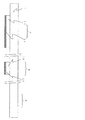
(実施例1)
液晶表示装置の画素を形成する側の基板を、本発明の実施例として説明する。図1は、液晶表示装置の画素を形成する側の基板の薄膜トランジスタ回路装置の全体構成の一部を模式的に示した図で、図2〜図9は、薄膜トランジスタ回路装置の一部を模式的に示した工程断面図である。
(Example 1)
A substrate on a pixel forming side of a liquid crystal display device will be described as an embodiment of the present invention. FIG. 1 is a diagram schematically showing a part of the entire configuration of the thin film transistor circuit device on the substrate on the pixel forming side of the liquid crystal display device, and FIGS. 2 to 9 schematically show a part of the thin film transistor circuit device. It is process sectional drawing shown in.
本発明を液晶表示装置以外の薄膜トランジスタ回路装置に適用できることは言うまでもない。 It goes without saying that the present invention can be applied to thin film transistor circuit devices other than liquid crystal display devices.
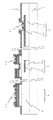
図1に示すように、薄膜トランジスタ回路装置100は、横方向にゲート配線2、ゲート端子3が設けられ、基板の最外周領域には静電保護配線4が形成されている。ゲート配線2はゲート端子3を通過し、ゲート配線22となって静電保護素子19を介して静電保護配線4に接続されている。薄膜トランジスタ回路装置100には、ゲート配線2に直交してドレイン配線7が設けられている。ドレイン配線7もドレイン端子8を通過し、ドレイン配線27となって静電保護素子19を介して静電保護配線4に接続されている。ゲート配線2とドレイン配線7とが交差する領域に薄膜トランジスタ10が設けられている。薄膜トランジスタ10のゲート端はゲート配線に接続され薄膜トランジスタ10のドレイン端子8はドレイン配線7に接続されソース端は画素電極(不図示)に接続されている。静電保護素子19は、薄膜トランジスタ10と同じ構造のトランジスタで構成されている。
As shown in FIG. 1, the thin film
図1では、I−I’で囲われた内部領域が主回路領域となり液晶表示装置に使用する薄膜トランジスタ回路装置の場合は、表示素子領域となっている。 In FIG. 1, the inner region surrounded by I-I ′ is the main circuit region, and in the case of a thin film transistor circuit device used for a liquid crystal display device, it is a display element region.
図1の薄膜トランジスタ回路装置は、液晶表示装置の基板を形成するもので、静電保護素子19は、薄膜トランジスタ回路装置の製造時の静電保護に使われている。液晶表示装置を製造する段階ではJ−J’の部分で基板を切断する。図1には示していないが、ゲート端子3およびドレイン端子8と表示素子領域との間に、更に静電保護回路やドライバー回路等の回路が形成される場合がある。これらの静電保護回路・ドライバー回路を含めて外部回路領域と称す。静電保護素子19と同様には、回路領域に形成される薄膜トランジスタも主回路領域に形成される薄膜トランジスタ10と同じ構造のトランジスタで構成されている。
The thin film transistor circuit device of FIG. 1 forms a substrate of a liquid crystal display device, and the
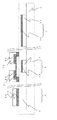
図2〜12は、ドレイン配線7およびドレイン端子8、薄膜トランジスタ10およびゲート配線2およびゲート端子3の各断面を薄膜トランジスタ回路装置の製造工程順に模式的に示した工程断面図である。各図において左からドレイン配線およびドレイン端子形成領域A、薄膜トランジスタ形成領域B、ゲート配線およびゲート端子領域Cの順に描いている。
2 to 12 are process sectional views schematically showing respective sections of the
まず、ガラスからなる透明基板1上に、ネオジムを2原子%含む膜厚200〜400nmのアルミニウム合金膜およびニオブを5〜15原子%含む膜厚50〜100nmのモリブデン合金膜をこの順に成膜し、下層がアルミニウム合金膜で上層がモリブデン合金膜である積層膜を形成した。積層膜を通常のフォトリソ法で形成したフォトレジストをマスクに、りん酸:硝酸:酢酸のエッチング液を用いたウェットエッチング法でゲート配線2、ゲート端子3及び静電保護配線4(図示せず)を形成した(第1フォトリソグラフィー工程)。ゲート配線2、ゲート端子3及び静電保護配線4(図示せず)は、下層がアルミニウム合金層31で上層がモリブデン合金層32の積層構造をしている(図2)。
First, on a
透明基板1として用いるガラスは、薄膜トランジスタ10を高温ポリシリコン法で形成する場合は石英ガラスのような耐熱性のあるガラスを用い、低温ポリシリコン法あるいはアモルファスシリコン法で形成する場合はアルカリガラスや無アルカリガラスが用いられる。本実施例ではアモルファスシリコン法を用いたカラー薄膜トランジスタ液晶表示装置用の薄膜トランジスタ回路装置を基板上に形成する例であるので、無アルカリガラスを用いた。
The glass used as the
次に、膜厚200〜600nmの窒化膜5、膜厚100〜300nmのアモルファスシリコン(以下、a−Siと略す)膜61、膜厚20〜70nmのn+型アモルファスシリコン(以下、n+型a−Siと略す)膜62、膜厚200〜500nmのクロム(Cr)膜70をこの順に成膜した(図3)。
Next, the
薄膜トランジスタ10のゲート絶縁膜となる窒化膜5は、窒化膜以外に酸窒化膜や酸化膜等の絶縁膜が使用できる。
As the
次に、クロム膜70の上にハーフトーンマスクを用いフォトリソ法によりレジストパターン58、59を形成した。レジストパターン58はドレイン端子8を含むドレイン配線の形成領域A上に、レジストパターン59は薄膜トランジスタ形成領域B上にそれぞれ形成した。
Next, resist
このとき、レジストパターン58および59はハーフトーン若しくはグレートーンマスクを用いて形成することが好ましい。
At this time, the resist
ハーフトーン若しくはグレートーンマスクは、完全露光部、遮光部以外に薄膜トランジスタ10のチャネル領域に対応する領域を半透過領域とするパターンとなっている。この結果、薄膜トランジスタ形成領域Bに形成されたレジストパターン59の膜厚は、薄膜トランジスタ10のチャネルが形成される領域の膜厚が0.5〜1.0μm、それ以外の膜厚が1.5〜2.0μmとなる。
The half-tone or gray-tone mask has a pattern in which a region corresponding to the channel region of the
次に、レジストパターン58、59をマスクとして、例えば、硝酸セリウムアンモニウム及び硝酸の混合液を用いてクロム膜70をエッチング除去した(図4)。
Next, using the resist
次に、レジストパターン58、59をマスクとして、n+型a−Si膜62及びa−Si膜61を順次ドライエッチングにより除去した(図5)。
Next, using the resist
次に、レジストパターン59の内の薄膜トランジスタ10のチャネル領域に対応する薄い部分を除去できる時間だけ酸素プラズマアッシングによりレジストパターン58、59を厚さ方向にエッチングした。これによりレジストパターン58、59は、それぞれ膜厚は0.5〜1.0μmのレジストパターン88、89および90となる(図6)。
Next, the resist
次に、レジストパターン88、89および90をマスクとしてクロム膜70を選択的にドライエッチングにより除去してドレイン端子電極73および薄膜トランジスタ10のドレイン電極74およびソース電極75を形成した(図7)。
Next, the chromium film 70 was selectively removed by dry etching using the resist
次に、レジストパターン88、89および90を除去した後、続いて、ドレイン端子電極73、ドレイン電極74、ソース電極75をマスクとして薄膜トランジスタ10のチャネル領域のn+型a−Si膜62とa−Si膜61の一部を厚さ方向にドライエッチングを用いてエッチング除去した(第2フォトリソグラフィー工程)。次に、膜厚100〜300nmの窒化膜からなる保護膜11を基板表面に形成し、続いて、フォトリソ工程を用いてドレイン端子8、薄膜トランジスタ10のソース電極75およびゲート端子上の絶縁膜をエッチング除去して開口12、13、14を形成した。このとき、ドレイン端子8および薄膜トランジスタ10のソース電極75に対応する開口12および13は、保護膜11をエッチング除去して形成され、ゲート端子3に対応する開口14は、保護膜11及び窒化膜5をエッチング除去して形成されている(第3フォトリソグラフィー工程)(図8)。
Next, after removing the resist
保護膜11は、窒化膜以外に酸化膜、酸窒化膜等の絶縁膜を用いることができることは言うまでもない。 Needless to say, the protective film 11 may be an insulating film such as an oxide film or an oxynitride film in addition to the nitride film.
最後に、スパッタ法で、厚さ30〜100nmのITO膜を成膜し、その後、フォトリソ工程を用いてエッチングマスクとなるフォトレジストパターンを形成し、次に、ドライエッチングを用いてITO膜をパターンニングし、ドレイン端子電極15、画素電極16、ゲート端子電極17を形成した(第4フォトリソグラフィー工程)(図9)。
Finally, an ITO film having a thickness of 30 to 100 nm is formed by sputtering, and then a photoresist pattern to be an etching mask is formed by using a photolithography process, and then the ITO film is patterned by using dry etching. The
以上のようにして薄膜トランジスタ回路装置が形成された。図9に示すように、ゲート端子3の電極構造は、下層から順にネオジムを含むアルミニウム合金、ニオブを含むモリブデン合金、ITOである。この場合、ニオブを含むモリブデン合金は、ニオブの含有率が5〜20原子%であることが好ましい。
A thin film transistor circuit device was formed as described above. As shown in FIG. 9, the electrode structure of the
尚、ITOに代えてIZOあるいはIZTO等を用いても同様の効果が得られる。 The same effect can be obtained by using IZO or IZTO instead of ITO.
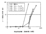
ITO、IZOあるいはIZTOとネオジムを含むアルミニウム合金との間にモリブデン系合金を挟むことによりITO、IZOあるいはIZTOとAlとの間で発生する電池作用が防止でき、かつ、ITO、IZOあるいはIZTOとの間の接触抵抗が小さくなる。しかしながら、ITO、IZOあるいはIZTOは水分を通し易く、モリブデン系合金上をITO、IZOあるいはIZTOが覆う構造ではあっても、モリブデン系合金には耐湿性が求められる。ここで、モリブデンにニオブを5〜20原子%含有させることによる著しい効果を、グラフを用いて説明する。 By interposing a molybdenum alloy between ITO, IZO or IZTO and an aluminum alloy containing neodymium, the battery action generated between ITO, IZO or IZTO and Al can be prevented, and with ITO, IZO or IZTO The contact resistance between them becomes small. However, ITO, IZO, or IZTO can easily pass moisture, and the molybdenum-based alloy is required to have moisture resistance even if the molybdenum-based alloy is covered with ITO, IZO, or IZTO. Here, the remarkable effect by containing 5-20 atomic% of niobium in molybdenum is demonstrated using a graph.
図10は、ニオブを含むモリブデン合金中のニオブの割合を変化させたときの高温多湿試験による合金抵抗値の経時変化を示したものである(横軸および縦軸は対数目盛)。ニオブを含まない純モリブデンでは約30時間経過すると合金抵抗値が増大し始める。また、ニオブを5、10、15原子%含有させた合金では、5原子%では約30時間経過したときに増加の兆候が観察されたが、ニオブを10、15原子%含有させた合金では全く抵抗値に変化は観察されなかった。ニオブを10、15原子%含有させた合金は、約100時間経過した時点から抵抗値の増大が観察された。従って、耐湿性は、モリブデンにニオブを5原子%以上含有させることが好ましく、10原子%以上含有させることがより好ましいことがわかる。 FIG. 10 shows the change over time in the alloy resistance value by the high temperature and humidity test when the proportion of niobium in the molybdenum alloy containing niobium is changed (the horizontal axis and the vertical axis are logarithmic scales). With pure molybdenum containing no niobium, the alloy resistance value starts to increase after about 30 hours. In addition, in the alloy containing 5, 10, 15 atomic% of niobium, signs of increase were observed after about 30 hours at 5 atomic%, but in the alloy containing 10, 15 atomic% of niobium, No change in resistance value was observed. In the alloy containing niobium at 10 and 15 atomic%, an increase in resistance value was observed after about 100 hours. Therefore, it can be seen that the moisture resistance is preferably 5 atomic% or more and more preferably 10 atomic% or more in molybdenum.
ニオブを15原子%以上含有させた場合も抵抗値の変化はニオブを10原子%、15原子%含有させた場合との差異は見られなかった。 Even when niobium was contained in an amount of 15 atomic% or more, the change in resistance value was not different from that in the case where niobium was contained at 10 atomic% or 15 atomic%.
図11は、ニオブを含むモリブデン合金をりん酸:硝酸:酢酸でウェットエッチングする際のニオブを含むモリブデン合金とネオジムを含むアルミニウム合金のエッチングレート比のモリブデンにニオブを含ませる割合による変化を示している。理想的には、ニオブを含むモリブデン合金とネオジムを含むアルミニウム合金との積層膜をウェットエッチングするので、良好なエッチング形状を得る為にはニオブを含むモリブデン合金とネオジムを含むアルミニウム合金のエッチングレートがほぼ等しくなることが好ましい。従って、ニオブを含むモリブデン合金とネオジムを含むアルミニウム合金とのエッチングレート比は、1.5〜0.5であることが好ましく、1.25〜0.75であることがより好ましい。上記の条件は、モリブデンにニオブを5〜15原子%含有させる、あるいは、5〜10原子%含有させることで達成できる。また、りん酸:硝酸:酢酸の成分調整により、エッチングレート比を調整することが可能であり、特に耐食性を優先する必要がある場合は、モリブデンにニオブを20原子%含ませることも可能である。 FIG. 11 shows the change in the etching rate ratio between the molybdenum alloy containing niobium and the aluminum alloy containing neodymium when the molybdenum alloy containing niobium is wet-etched with phosphoric acid: nitric acid: acetic acid according to the ratio of niobium contained in molybdenum. Yes. Ideally, a laminated film of a molybdenum alloy containing niobium and an aluminum alloy containing neodymium is wet etched, so in order to obtain a good etching shape, the etching rate of the molybdenum alloy containing niobium and the aluminum alloy containing neodymium is It is preferable that they are approximately equal. Therefore, the etching rate ratio between the molybdenum alloy containing niobium and the aluminum alloy containing neodymium is preferably 1.5 to 0.5, and more preferably 1.25 to 0.75. The above conditions can be achieved by containing 5 to 15 atomic percent of niobium in molybdenum or 5 to 10 atomic percent. Moreover, it is possible to adjust the etching rate ratio by adjusting the phosphoric acid: nitric acid: acetic acid components, and when it is necessary to give priority to corrosion resistance, it is also possible to include 20 atomic% of niobium in molybdenum. .
図10、11の結果から、モリブデンにニオブを5〜20原子%含ませれば最適なニオブを含むモリブデン合金となる。本発明を適用する液晶表示装置が、エッチング形状を優先と場合はモリブデンにニオブを5〜10原子%含ませると最適となり、耐食性を優先する場合はモリブデンにニオブを10〜15原子%含ませると最適となり、特に耐食性を優先する場合はモリブデンにニオブを15〜20原子%含ませると最適となる。 From the results shown in FIGS. 10 and 11, when molybdenum contains 5 to 20 atomic% of niobium, an optimal molybdenum alloy containing niobium is obtained. The liquid crystal display device to which the present invention is applied is optimal when 5-10 atomic percent of niobium is included in molybdenum when the etching shape is prioritized, and when 10-15 atomic percent of niobium is included in molybdenum when corrosion resistance is prioritized. In particular, when priority is given to corrosion resistance, it is optimal to include 15 to 20 atomic percent of niobium in molybdenum.
本実施例では、表示素子部の構造も最も単純な構成を示しているために、表示素子領域のゲート配線2やドレイン配線7は同一の層に形成した構造で説明しているが、ゲート端子3およびドレイン端子8に加わる静電から表示素子やドライバー回路を構成するトランジスタを保護する静電保護回路を設けた場合や横電界型の用に画素部の構造が複雑な場合、ゲート電極とゲート配線/ドレイン電極とドレイン配線7を別の層に作りこむ場合がある。図31に一方の薄膜トランジスタ10のゲート配線と他方の薄膜トランジスタ10の一端とを接合する場合を例に模式図を示す。図31(a)は、該構成の平面図を示し、図31(b)は、図31(a)のa−a’の断面を示す図である。
In this embodiment, since the structure of the display element portion also shows the simplest structure, the
図31(a)では2個の薄膜トランジスタ10が並列して形成され、一方の薄膜トランジスタ10のゲート配線2と他方の薄膜トランジスタ10の一方の電極とが接続され、他方の薄膜トランジスタ10のゲート配線2と一方の薄膜トランジスタ10の一方の電極とが接続されている。図31(b)は、図31(a)のA−A’断面図である。基板1上にネオジムを含むアルミニウム合金層31とニオブを含むモリブデン合金層32の積層構造のゲート配線2が形成されている。ゲート配線2上には、ゲート絶縁膜となる窒化膜5とa−Si膜61およびn+a−Si膜62の積層構造である薄膜トランジスタ10のボディーと該ボディー上に形成されたニオブを含むモリブデン合金層121、ネオジムを含むアルミニウム合金層122およびニオブを含むモリブデン合金層123の積層構造の電極が形成されている。保護膜11が表面全面を覆うように形成され、電極上の保護膜11には電極を露出する第1の開口部が形成されている。更に、保護膜11と窒化膜5には、ゲート配線2の表面を露出するための第2の開口部が形成され、第1の開口部と第2の開口部とを介してゲート配線2と電極とを接続する接続配線77が形成されている。
(実施例2)
次に、本発明の実施例2を図12に示す。図12は、図9のD部の拡大図で、ゲート端子3のITOとニオブを含むモリブデン合金の界面に、ニオブの酸化物が形成されている。
In FIG. 31A, two
(Example 2)
Next,
ニオブの酸化物からなる層18は、ITOをスパッタで成膜する際、アルゴンに酸素を添加することで実現できる。 The layer 18 made of niobium oxide can be realized by adding oxygen to argon when ITO is formed by sputtering.
実施例2では、スパッタを用いて厚さ30〜100nmのITOを成膜した。スパッタ条件は、圧力は、0.2〜1.0Pa、DCパワーは、1〜2KW、酸素流量は、アルゴン流量の0.1〜2%が好ましい条件であったが、装置等の違いでこの条件以外に最適値がある場合があり、適宜決定することができることはいうまでもない。 In Example 2, an ITO film having a thickness of 30 to 100 nm was formed by sputtering. The sputtering conditions were preferably such that the pressure was 0.2 to 1.0 Pa, the DC power was 1 to 2 kW, and the oxygen flow rate was 0.1 to 2% of the argon flow rate. Needless to say, there may be an optimum value other than the conditions, which can be determined as appropriate.
アルゴンに若干の酸素を添加するこれにより、スパッタ開始直後にニオブを含むモリブデン合金の表面に、約1〜5nmの薄いニオブの酸化物からなる層18が形成される。ニオブの酸化物からなる層18は不働体であるのでバリア膜の役割をはたし、モリブデン及びその下のAlの腐食を阻止することができる。尚、アルゴンガスに変えて、ヘリウム等の不活性ガスを用いることができることはいうまでもない。 By adding a slight amount of oxygen to argon, a layer 18 made of a thin niobium oxide of about 1 to 5 nm is formed on the surface of the molybdenum alloy containing niobium immediately after the start of sputtering. Since the layer 18 made of niobium oxide is a passive material, it plays a role of a barrier film, and can prevent corrosion of molybdenum and the underlying Al. Needless to say, an inert gas such as helium can be used instead of the argon gas.
尚、ニオブの酸化物からなる層18は、酸素を含む雰囲気中で加熱した後、ITOをアルゴン雰囲気中でスパッタしても形成することができることはいうまでもない。ITOをスパッタする前に下地加熱を行う場合、スパッタ装置内を減圧せず大気雰囲気あるいはアルゴンに酸素を含有させ下地加熱し、その後減圧してスパッタを行えば工程を増やすことなくニオブの酸化物からなる層18を形成できる。
(実施例3)
次に、本発明の実施例3について図13、14を用いて説明する。実施例1では、ネオジムを含むアルミニウム合金とニオブを含むモリブデン合金の積層構造をゲート配線のみに適用したが、本実施例ではドレイン配線にも適用したものである。この場合、ドレイン配線はその下面がアモルファスシリコン膜と接触するので、アルミニウムとシリコン膜との共晶反応を防止するために、ネオジムを含むアルミニウム合金下にもニオブを含むモリブデン合金を設ける3層構造となる。アモルファスシリコン層との共晶反応を防止するためのモリブデン合金層は、表面が露出することがないので純モリブデン層であっても問題はない。
Needless to say, the layer 18 made of niobium oxide can be formed by heating in an atmosphere containing oxygen and then sputtering ITO in an argon atmosphere. If the substrate is heated before sputtering ITO, the substrate is heated without adding pressure to the atmosphere, or the atmosphere is heated by adding oxygen to the atmosphere or argon. A layer 18 can be formed.
(Example 3)
Next, a third embodiment of the present invention will be described with reference to FIGS. In the first embodiment, the laminated structure of the aluminum alloy containing neodymium and the molybdenum alloy containing niobium is applied only to the gate wiring, but in this embodiment, it is also applied to the drain wiring. In this case, since the lower surface of the drain wiring is in contact with the amorphous silicon film, a three-layer structure in which a molybdenum alloy containing niobium is also provided under an aluminum alloy containing neodymium in order to prevent a eutectic reaction between aluminum and the silicon film. It becomes. Since the surface of the molybdenum alloy layer for preventing eutectic reaction with the amorphous silicon layer is not exposed, there is no problem even if it is a pure molybdenum layer.
本実施例ではシリコン膜としてアモルファスシリコン膜を用いているが、単結晶シリコンあるいは多結晶シリコンでも同様の結果になることはいうまでもない。 In this embodiment, an amorphous silicon film is used as the silicon film, but it goes without saying that the same result can be obtained with single crystal silicon or polycrystalline silicon.
実施例1の図3ではクロム膜70を成膜したが、本実施例では、ニオブを5〜15原子%含む膜厚50〜100nmのモリブデン合金膜121、ネオジムを2原子%含む膜厚200〜400nmのアルミニウム合金膜122およびニオブを5〜15原子%含む膜厚50〜100nmのモリブデン合金膜123をこの順に成膜した(図13)。 In FIG. 3 of the first embodiment, the chromium film 70 is formed. However, in this embodiment, the molybdenum alloy film 121 having a thickness of 50 to 100 nm containing 5 to 15 atomic% of niobium and the film thickness of 200 to 200 containing 2 atomic% of neodymium. A 400 nm aluminum alloy film 122 and a 50-100 nm thick molybdenum alloy film 123 containing 5-15 atomic% of niobium were formed in this order (FIG. 13).
次に、図4と同様に、モリブデン合金膜123の上にグレートーンマスクを用いフォトリソ法によりレジストパターンを、ドレイン端子を含むドレイン配線の形成領域A上と薄膜トランジスタ形成領域B上とにそれぞれ形成した。これらのレジストは図4の説明と同様に、薄膜トランジスタ10のチャネル領域に対応する領域を半透過領域とするハーフトーン若しくはグレートーンマスクを用いて形成することが好ましい。本実施例においても薄膜トランジスタ10のチャネルが形成される領域の膜厚が0.5〜1.0μm、それ以外の膜厚が1.5〜2.0μmのレジストパターンが形成された。
Next, as in FIG. 4, resist patterns were formed on the molybdenum alloy film 123 on the formation region A of the drain wiring including the drain terminal and the thin film transistor formation region B by a photolithography method using a gray-tone mask. . Similar to the description of FIG. 4, these resists are preferably formed using a halftone or gray tone mask in which a region corresponding to the channel region of the
次に、レジストパターンをマスクとして、例えば、りん酸:硝酸:酢酸のエッチング液を用いたウェットエッチング法により、レジストパターンに覆われていない、モリブデン合金膜121、アルミニウム合金膜122およびモリブデン合金膜123をエッチングした。 Next, using the resist pattern as a mask, for example, a molybdenum alloy film 121, an aluminum alloy film 122, and a molybdenum alloy film 123 that are not covered with the resist pattern by a wet etching method using an etching solution of phosphoric acid: nitric acid: acetic acid. Was etched.
その後、レジストパターンをマスクとして、n+型a−Si膜62及びa−Si膜61を順次ドライエッチングにより除去した。 Thereafter, using the resist pattern as a mask, the n + -type a-Si film 62 and the a-Si film 61 were sequentially removed by dry etching.
次に、図6と同様に、レジストパターンの内の薄膜トランジスタ10のチャネル領域に対応する薄い部分を除去できる時間だけ酸素プラズマアッシングによりレジストパターンを厚さ方向にエッチングし、薄膜トランジスタ10のチャネル領域が形成される領域のレジストパターンが除去される。
Next, as in FIG. 6, the resist pattern is etched in the thickness direction by oxygen plasma ashing for a time that can remove a thin portion of the resist pattern corresponding to the channel region of the
次に、図7と同様に、残っているレジストパターンをマスクとして薄膜トランジスタ10のチャネル形成領域のモリブデン合金膜121、アルミニウム合金膜122およびモリブデン合金膜123をエッチング除去した。
Next, as in FIG. 7, the molybdenum alloy film 121, the aluminum alloy film 122, and the molybdenum alloy film 123 in the channel formation region of the
次に、図8と同様に、レジストパターンを除去した後、続いて、ドレイン電極、ソース電極をマスクとしてn+型a−Si膜62とa−Si膜61の一部を厚さ方向に除去した(第2フォトリソグラフィー工程)。次に、膜厚100〜300nmの窒化膜からなる保護膜11を基板表面に形成し、続いて、フォトリソ工程を通してドレイン端子8、薄膜トランジスタ10のソース電極およびゲート端子3上の絶縁膜をエッチング除去して開口を形成した。このとき、ドレイン端子8および薄膜トランジスタ10のソース電極に対応する開口は、保護膜11をエッチング除去して形成され、ゲート端子3に対応する開口14は、保護膜11及び絶縁膜5をエッチング除去して形成されている(第3フォトリソグラフィー工程)。
Next, as in FIG. 8, after removing the resist pattern, the n + -type a-Si film 62 and a part of the a-Si film 61 are removed in the thickness direction using the drain electrode and the source electrode as a mask. (Second photolithography step). Next, a protective film 11 made of a nitride film having a thickness of 100 to 300 nm is formed on the substrate surface, and subsequently, the
最後に、スパッタ法で、厚さ30〜100nmのITOの透明導電膜を成膜し、その後、フォトリソ工程を通してパターンニングし、ドレイン端子電極15、画素電極16、ゲート端子電極17を形成した(第4フォトリソグラフィー工程)(図14)。
Finally, an ITO transparent conductive film having a thickness of 30 to 100 nm is formed by sputtering, and then patterned through a photolithography process to form the
以上のようにして薄膜トランジスタ回路装置が形成された。図14に示すように、ドレイン配線およびドレイン端子8、ゲート配線およびゲート端子3および、ソース・ドレイン電極の電極構造は、下層から順にニオブを含むモリブデン合金、ネオジムを含むアルミニウム合金、ニオブを含むモリブデン合金およびITOである。この場合、ニオブを含むモリブデン合金は、ニオブの含有率が5〜20原子%であることが好ましい。
(実施例4)
図15〜22は、本実施例のドレイン配線7およびドレイン端子8、薄膜トランジスタ10およびゲート配線2およびゲート端子3の各断面を薄膜トランジスタ回路装置の製造工程順に模式的に示した工程断面図である。各図において左からドレイン配線およびドレイン端子形成領域A、薄膜トランジスタ形成領域B、ゲート配線およびゲート端子領域Cの順に描いている。
A thin film transistor circuit device was formed as described above. As shown in FIG. 14, the drain wiring and drain
Example 4
15 to 22 are process cross-sectional views schematically showing respective cross sections of the
まず、ガラスからなる透明基板1上に、ネオジムを2原子%含む膜厚200〜400nmのアルミニウム合金膜およびニオブを5〜15原子%含む膜厚50〜100nmのモリブデン合金膜をこの順に成膜し、下層がアルミニウム合金膜で上層がモリブデン合金膜である積層膜を形成した。積層膜を通常のフォトリソ法で形成したフォトレジストをマスクに、りん酸:硝酸:酢酸のエッチング液を用いたウェットエッチング法でゲート配線2、ゲート端子3及び静電保護配線4(図示せず)を形成した(第1フォトリソグラフィー工程)(図15)。ゲート配線2、ゲート端子3及び静電保護配線4(図示せず)は、下層がアルミニウム合金層31で上層がモリブデン合金層32の積層構造をしている。
First, on a
本実施例も実施例1同様にカラー薄膜トランジスタ液晶表示装置用の薄膜トランジスタ回路装置を基板上に形成する例であるので、無アルカリガラスを用いた。 Since this example is also an example in which a thin film transistor circuit device for a color thin film transistor liquid crystal display device is formed on a substrate in the same manner as in Example 1, non-alkali glass was used.
次に、膜厚200〜600nmの窒化膜5、膜厚100〜300nmのa−Si膜61、膜厚20〜70nmのn+型a−Si膜62、ニオブを5〜15原子%含む膜厚200〜500nmのモリブデン合金膜40をこの順に成膜した(図16)。
Next, a
次に、モリブデン合金膜40の上にグレートーンマスクを用いてフォトリソ法によりレジストパターン58、59を形成した。レジストパターン58はドレイン端子を含むドレイン配線の形成領域A上に形成し、レジストパターン59は薄膜トランジスタ形成領域B上にそれぞれ形成した。
Next, resist
このとき、レジストパターン58および59はハーフトーン若しくはグレートーンマスクを用いて形成することが好ましい。
At this time, the resist
ハーフトーン若しくはグレートーンマスクは、完全露光部、遮光部以外に薄膜トランジスタ10のチャネル領域に対応する領域を半透過領域とするパターンとなっている。この結果、薄膜トランジスタ形成領域Bに形成されたレジストパターン59の膜厚は、薄膜トランジスタ10のチャネルが形成される領域の膜厚が0.5〜1.0μm、それ以外の膜厚が1.5〜2.0μmとなる。
The half-tone or gray-tone mask has a pattern in which a region corresponding to the channel region of the
次に、レジストパターン58、59をマスクとして、例えば、りん酸:硝酸:酢酸のエッチング液を用いたウェットエッチング法でモリブデン合金層40をエッチング除去した(図17)。
Next, using the resist
次に、レジストパターン58、59をマスクとして、n+型a−Si膜62及びa−Si膜61を順次ドライエッチングにより除去した(図18)。
Next, using the resist
次に、レジストパターン59の内の薄膜トランジスタ10のチャネル領域に対応する薄い部分を除去できる時間だけ酸素プラズマアッシングによりレジストパターン58、59を厚さ方向にエッチングした(図19)。これによりレジストパターン58、59は、それぞれ膜厚は0.5〜1.0μmのレジストパターン88、89および90となる。
Next, the resist
次に、レジストパターン88、89および90をマスクとして薄膜トランジスタ10のチャネル領域に露出しているモリブデン合金層40を選択的にドライエッチングにより除去してドレイン端子電極73および薄膜トランジスタ10のドレイン電極74およびソース電極75を形成した(図20)。
Next, the molybdenum alloy layer 40 exposed in the channel region of the
次に、レジストパターン88、89および90を除去し、続いてドレイン電極74、ソース電極75をマスクとしてn+型a−Si膜62とa−Si膜61の一部を厚さ方向に除去した(第2フォトリソグラフィー工程)。次に、膜厚100〜300nmの窒化膜からなる保護膜11を基板表面に形成し、続いて、フォトリソ工程を用いてドレイン端子8、薄膜トランジスタ10のソース電極75およびゲート端子3上の絶縁膜をエッチング除去して開口12、13、14を形成した。このとき、ドレイン端子8および薄膜トランジスタ10のソース電極75に対応する開口12および13は、保護膜11をエッチング除去して形成され、ゲート端子3に対応する開口14は、保護膜11及び窒化膜5をエッチング除去して形成されている(第3フォトリソグラフィー工程)(図21)。
Next, the resist
最後に、スパッタ法で、厚さ30〜100nmのITO膜を成膜し、その後、フォトリソ工程を用いてエッチングマスクとなるフォトレジストパターンを形成し、次に、ドライエッチングを用いてITO膜をパターンニングし、ドレイン端子電極15、画素電極16、ゲート端子電極17を形成した(第4フォトリソグラフィー工程)(図22)。
(実施例5)
上述の実施例では、4PRで行ったが、5PRで行うこともできる。
Finally, an ITO film having a thickness of 30 to 100 nm is formed by sputtering, and then a photoresist pattern to be an etching mask is formed by using a photolithography process, and then the ITO film is patterned by using dry etching. The
(Example 5)
In the above-described embodiment, the process is performed at 4PR, but can be performed at 5PR.
図23〜30は、ドレイン配線7およびドレイン端子8、薄膜トランジスタ10およびゲート配線2およびゲート端子3の各断面を薄膜トランジスタ回路装置の製造工程順に模式的に示した工程断面図である。各図において左からドレイン配線およびドレイン端子形成領域A、薄膜トランジスタ形成領域B、ゲート配線およびゲート端子領域Cの順に描いている。
23 to 30 are process sectional views schematically showing respective sections of the
まず、ガラスからなる透明基板1上に、ネオジムを2原子%含む膜厚200〜400nmのアルミニウム合金膜21およびニオブを5〜15原子%含む膜厚50〜100nmのモリブデン合金膜をこの順に成膜し、下層がアルミニウム合金膜で上層がモリブデン合金膜である積層膜を形成した。積層膜を通常のフォトリソ法で形成したフォトレジストをマスクに、りん酸:硝酸:酢酸のエッチング液を用いたウェットエッチング法でゲート配線2、ゲート端子3及び静電保護配線4(図示せず)を形成した(第1フォトリソグラフィー工程)(図23)。ゲート配線2、ゲート端子3及び静電保護配線4(図示せず)は、下層がアルミニウム合金層31で上層がモリブデン合金層32の積層構造をしている。
First, on a
本実施例も実施例1同様にカラー薄膜トランジスタ表示装置用の薄膜トランジスタ回路装置を基板上に形成する例であるので、無アルカリガラスを用いた。 Since this example is also an example in which a thin film transistor circuit device for a color thin film transistor display device is formed on a substrate in the same manner as in Example 1, alkali-free glass was used.
次に、膜厚200〜600nmの窒化膜5、膜厚100〜300nmのa−Si膜61、膜厚20〜70nmのn+型a−Si膜62をこの順に成膜した。
Next, a
次に、n+型a−Si膜62の薄膜トランジスタ形成領域B上にフォトリソ法を用いてレジストパターン57を形成した(図24)。レジストパターン57をマスクとして、n+型a−Si膜62およびa−Si膜61をドライエッチング法を用いて除去した(第2フォトリソグラフィー工程)。
Next, a resist
次に、レジストパターン57を除去後、ニオブを5〜15原子%含む膜厚200〜500nmのモリブデン合金膜40を形成した(図25)。
Next, after removing the resist
次に、モリブデン合金膜40の上にフォトリソ法によりレジストパターン88、89および90を形成した。レジストパターン88はドレイン端子を含むドレイン配線の形成領域A上に形成し、レジストパターン88および89は薄膜トランジスタ形成領域B上にそれぞれ形成した(図26)。
Next, resist
次に、レジストパターン88、89および90をマスクとして、例えば、りん酸:硝酸:酢酸のエッチング液を用いたウェットエッチング法でモリブデン合金層40をエッチング除去してドレイン端子電極73および薄膜トランジスタ10のドレイン電極74およびソース電極75を形成した(図27)(第3フォトリソグラフィー工程)。
Next, using the resist
次に、レジストパターン88、89および90を除去し、続いて、ドレイン端子電極73、ドレイン電極74、ソース電極75をマスクとしてn+型a−Si膜62とa−Si膜61の一部を厚さ方向に除去した(図28)。次に、膜厚100〜300nmの窒化膜からなる保護膜11を基板表面に形成し、続いて、フォトリソ工程を用いてドレイン端子8、薄膜トランジスタ10のソース電極75およびゲート端子3上の絶縁膜をエッチング除去して開口12、13、14を形成した(第4フォトリソグラフィー工程)(図29)。このとき、ドレイン端子8および薄膜トランジスタ10のソース電極75に対応する開口12および13は、保護膜11をエッチング除去して形成され、ゲート端子3に対応する開口14は、保護膜11及び絶縁膜5をエッチング除去して形成されている。
Next, the resist
最後に、スパッタ法で、厚さ30〜100nmのITO膜を成膜し、その後、フォトリソ工程を用いてエッチングマスクとなるフォトレジストパターンを形成し、次に、ドライエッチングを用いてITO膜をパターンニングし、ドレイン端子電極15、画素電極16、ゲート端子電極17を形成した(第5フォトリソグラフィー工程)(図30)。
(実施例6)
アルミニウム合金は、ウェットエッチングする際に完全に除去される必要がある。シリコンを含有するAl−Si合金は、ドライエッチングでは完全に除去できるがウェットエッチングでは表面に薄い層として残るので好ましくない。
Finally, an ITO film having a thickness of 30 to 100 nm is formed by sputtering, and then a photoresist pattern to be an etching mask is formed by using a photolithography process, and then the ITO film is patterned by using dry etching. The
(Example 6)
The aluminum alloy needs to be completely removed during wet etching. An Al—Si alloy containing silicon can be completely removed by dry etching, but is not preferable because it remains as a thin layer on the surface by wet etching.
ウェットエッチングで完全に除去できる不純物であればネオジム以外の不純物を含んでいても良いことは言うまでもない。 Needless to say, impurities other than neodymium may be included as long as they can be completely removed by wet etching.
ウェットエッチングで完全に除去できる点で、純アルミニウムあるいはアルミニウム−ネオジム合金が好ましく用いることができる。 Pure aluminum or an aluminum-neodymium alloy can be preferably used because it can be completely removed by wet etching.
更に、ウェットエッチングする際に完全に除去できれば、純アルミニウムあるいはアルミニウム系の合金以外に、銀を主体とする銀形の合金あるいは銅を主体とする銅系の合金であっても良いことは言うまでもない。 Furthermore, as long as it can be completely removed during wet etching, it is needless to say that other than pure aluminum or an aluminum-based alloy, a silver-based alloy mainly composed of silver or a copper-based alloy mainly composed of copper may be used. .
また、上述の実施形態においては、縦電界方式の液晶表示装置の薄膜トランジスタの構造について記したが、横電界方式等、液晶制御方式が異なる薄膜トランジスタの構造に用いても、上記実施形態と同様の効果が得られる。 Further, in the above-described embodiment, the structure of the thin film transistor of the vertical electric field type liquid crystal display device is described. Is obtained.
本発明の薄膜トランジスタ回路装置が形成された第1の基板と例えば共通配線が形成された第2の基板とを対向して配置し、液晶を狭持することで液晶表示装置が形成できる。 A liquid crystal display device can be formed by placing a first substrate on which a thin film transistor circuit device of the present invention is formed and a second substrate on which, for example, a common wiring is formed facing each other and sandwiching liquid crystal.
1 透明基板
2、22 ゲート配線
3 ゲート端子
4 静電保護配線
5 窒化膜
7 ドレイン配線
8 ドレイン端子
10 薄膜トランジスタ
11 保護膜
12、13、14 開口
15 ドレイン端子電極
16 画素電極
17 ゲート端子電極
18 ニオブの酸化物からなる層
19 静電保護素子
31、122 アルミニウム合金層
32 モリブデン合金層
70 クロム膜
57、58、59、88、89、90 レジストパターン
61 アモルファスシリコン(a−Si)膜
62 n+型アモルファスシリコン(n+型a−Siと略す)膜
73 ドレイン端子電極
74 ドレイン電極
75 ソース電極
77 接続配線
100 薄膜トランジスタ回路装置
121,123 モリブデン合金膜
122 アルミニウム合金膜
DESCRIPTION OF
Claims (30)
前記端子は絶縁膜で覆われた配線の一部を露出させ、該露出面に端子電極が形成された端子であり、
前記露出面がニオブを含むモリブデン合金であることを特徴とする薄膜トランジスタ回路装置。 A thin film transistor circuit device having wiring extending from a main circuit region formed at least in a central portion of a substrate to a terminal formed on an outer periphery of the substrate,
The terminal is a terminal in which a part of the wiring covered with an insulating film is exposed, and a terminal electrode is formed on the exposed surface,
A thin film transistor circuit device, wherein the exposed surface is a molybdenum alloy containing niobium.
前記薄膜トランジスタの電極あるいは前記配線上に形成された絶縁膜と、
前記絶縁膜に形成され下層の前記薄膜トランジスタの電極あるいは前記配線の少なくとも一部を露出する開口部と、
前記開口部に電極あるいは前記開口部間を接続する接続配線とを有し、
前記開口部に露出する前記薄膜トランジスタの電極あるいは前記配線を構成する金属がニオブを含むモリブデン合金であることを特徴とする薄膜トランジスタ回路装置。 A thin film transistor and a wiring formed in a main circuit region formed in the center of the substrate and an external circuit region formed in the outer periphery of the substrate;
An insulating film formed on the electrode of the thin film transistor or the wiring;
An opening formed in the insulating film and exposing at least part of the electrode of the underlying thin film transistor or the wiring;
Having an electrode or a connection wiring connecting between the openings in the opening,
A thin film transistor circuit device, wherein a metal constituting the electrode of the thin film transistor or the wiring exposed in the opening is a molybdenum alloy containing niobium.
少なくとも前記薄膜トランジスタの電極あるいは前記配線上に絶縁膜を形成する絶縁膜形成工程と、
前記絶縁膜に形成され下層の前記薄膜トランジスタの電極あるいは前記配線の少なくとも一部を露出して開口部を形成する開口部形成工程と、
前記開口部に電極あるいは前記開口部間を接続する接続配線を構成する導電膜を形成する金属膜形成工程とを有し、
前記開口部に露出する前記薄膜トランジスタの電極あるいは前記配線を構成する金属がニオブを含むモリブデン合金であることを特徴とする薄膜トランジスタ回路装置の製造方法。 A method of manufacturing a thin film transistor circuit device having a thin film transistor and a wiring formed in a main circuit region formed in a central portion of a substrate and an external circuit region formed in an outer periphery of the substrate,
An insulating film forming step of forming an insulating film on at least the electrode of the thin film transistor or the wiring; and
An opening forming step of forming an opening by exposing at least a part of the electrode of the thin film transistor or the wiring formed in the insulating film; and
A metal film forming step of forming a conductive film constituting an electrode or connection wiring connecting between the openings in the opening,
A method of manufacturing a thin film transistor circuit device, wherein a metal constituting the electrode of the thin film transistor or the wiring exposed in the opening is a molybdenum alloy containing niobium.
Priority Applications (7)
| Application Number | Priority Date | Filing Date | Title |
|---|---|---|---|
| US10/895,404 US7105896B2 (en) | 2003-07-22 | 2004-07-21 | Thin film transistor circuit device, production method thereof and liquid crystal display using the think film transistor circuit device |
| JP2004212977A JP2005057260A (en) | 2003-07-22 | 2004-07-21 | Thin-film transistor circuit device, method for manufacturing the same, and liquid crystal display device using the same |
| KR1020040057114A KR100702284B1 (en) | 2003-07-22 | 2004-07-22 | Thin film transistor circuit device and liquid crystal display using the thin film transistor circuit device |
| TW093121918A TWI253618B (en) | 2003-07-22 | 2004-07-22 | Thin film transistor circuit device, production method thereof and liquid crystal display using the thin film transistor circuit device |
| CNB2004100544435A CN100370349C (en) | 2003-07-22 | 2004-07-22 | Thin film transistor circuit device, production method thereof and liquid crystal display using the thin film transistor circuit device |
| US11/384,342 US7341898B2 (en) | 2003-07-22 | 2006-03-21 | Thin film transistor circuit device, production method thereof and liquid crystal display using the thin film transistor circuit device |
| KR1020060110237A KR20070003719A (en) | 2003-07-22 | 2006-11-09 | Method of production for thin film transistor circuit device |
Applications Claiming Priority (2)
| Application Number | Priority Date | Filing Date | Title |
|---|---|---|---|
| JP2003277459 | 2003-07-22 | ||
| JP2004212977A JP2005057260A (en) | 2003-07-22 | 2004-07-21 | Thin-film transistor circuit device, method for manufacturing the same, and liquid crystal display device using the same |
Publications (2)
| Publication Number | Publication Date |
|---|---|
| JP2005057260A true JP2005057260A (en) | 2005-03-03 |
| JP2005057260A5 JP2005057260A5 (en) | 2007-08-02 |
Family
ID=34277594
Family Applications (1)
| Application Number | Title | Priority Date | Filing Date |
|---|---|---|---|
| JP2004212977A Pending JP2005057260A (en) | 2003-07-22 | 2004-07-21 | Thin-film transistor circuit device, method for manufacturing the same, and liquid crystal display device using the same |
Country Status (5)
| Country | Link |
|---|---|
| US (2) | US7105896B2 (en) |
| JP (1) | JP2005057260A (en) |
| KR (2) | KR100702284B1 (en) |
| CN (1) | CN100370349C (en) |
| TW (1) | TWI253618B (en) |
Cited By (3)
| Publication number | Priority date | Publication date | Assignee | Title |
|---|---|---|---|---|
| JP2007048878A (en) * | 2005-08-09 | 2007-02-22 | Mitsubishi Electric Corp | Semiconductor device |
| JP2008133529A (en) * | 2006-08-29 | 2008-06-12 | Rohm & Haas Electronic Materials Llc | Stripping method |
| US7888148B2 (en) | 2006-09-29 | 2011-02-15 | Samsung Electronics Co., Ltd. | Signal line for a display device, etchant, thin film transistor panel, and method for manufacturing the same |
Families Citing this family (11)
| Publication number | Priority date | Publication date | Assignee | Title |
|---|---|---|---|---|
| JP2005062802A (en) * | 2003-07-28 | 2005-03-10 | Advanced Display Inc | Method for manufacturing thin film transistor array substrate |
| KR101061850B1 (en) * | 2004-09-08 | 2011-09-02 | 삼성전자주식회사 | Thin film transistor array panel and manufacturing method thereof |
| TWI252587B (en) * | 2004-12-14 | 2006-04-01 | Quanta Display Inc | Method for manufacturing a pixel electrode contact of a thin-film transistors liquid crystal display |
| US20070259190A1 (en) * | 2006-05-02 | 2007-11-08 | Jau-Jier Chu | ITO transparent substrate with high resistance at low-temperature sputtering process and method for producing the same |
| US20070262311A1 (en) * | 2006-05-11 | 2007-11-15 | Toppoly Optoelectronics Corp. | Flat panel display and fabrication method and thereof |
| TW200820444A (en) * | 2006-10-27 | 2008-05-01 | Chunghwa Picture Tubes Ltd | Thin film transistor and fabrication method thereof |
| TWI374510B (en) | 2008-04-18 | 2012-10-11 | Au Optronics Corp | Gate driver on array of a display and method of making device of a display |
| KR101909139B1 (en) * | 2011-02-07 | 2018-12-19 | 삼성디스플레이 주식회사 | Thin film transistor array panel and manufacturing method thereof |
| KR20180028084A (en) | 2016-09-07 | 2018-03-16 | 삼성디스플레이 주식회사 | Display device |
| US9666482B1 (en) * | 2016-09-14 | 2017-05-30 | Infineon Technologies Ag | Self aligned silicon carbide contact formation using protective layer |
| CN110928085B (en) * | 2019-11-26 | 2021-01-15 | Tcl华星光电技术有限公司 | Array substrate and display panel |
Citations (6)
| Publication number | Priority date | Publication date | Assignee | Title |
|---|---|---|---|---|
| JPH10293321A (en) * | 1997-04-17 | 1998-11-04 | Mitsubishi Electric Corp | Liquid crystal display and its manufacture |
| JPH1138440A (en) * | 1997-07-17 | 1999-02-12 | Sharp Corp | Active matrix type liquid crystal display device and its production |
| JP2000284326A (en) * | 1999-03-30 | 2000-10-13 | Hitachi Ltd | Liquid crystal display device and its production |
| JP2000307118A (en) * | 1999-04-21 | 2000-11-02 | Matsushita Electric Ind Co Ltd | Thin-film transistor and manufacture thereof |
| JP2002327264A (en) * | 2001-04-26 | 2002-11-15 | Hitachi Metals Ltd | Sputtering target for forming thin film |
| JP2002365640A (en) * | 2001-03-26 | 2002-12-18 | Lg Phillips Lcd Co Ltd | Liquid crystal display device and manufacturing method therefor |
Family Cites Families (7)
| Publication number | Priority date | Publication date | Assignee | Title |
|---|---|---|---|---|
| JP3009438B2 (en) * | 1989-08-14 | 2000-02-14 | 株式会社日立製作所 | Liquid crystal display |
| US5530573A (en) * | 1993-05-27 | 1996-06-25 | Sharp Kabushiki Kaisha | Multiple domain liquid crystal display having a cell thickness divided by helical pitch equal to 1/8 or less |
| JPH0926598A (en) | 1995-07-10 | 1997-01-28 | Hitachi Ltd | Active matrix type liquid crystal display device |
| KR100239778B1 (en) * | 1996-12-03 | 2000-01-15 | 구본준 | Lcd device and its manufacturing method |
| JPH1187068A (en) * | 1997-07-15 | 1999-03-30 | Tdk Corp | Organic el element and manufacture thereof |
| JPH11259016A (en) * | 1998-03-13 | 1999-09-24 | Toshiba Corp | Manufacture of array substrate for display device |
| TWI255957B (en) * | 1999-03-26 | 2006-06-01 | Hitachi Ltd | Liquid crystal display device and method of manufacturing the same |
-
2004
- 2004-07-21 JP JP2004212977A patent/JP2005057260A/en active Pending
- 2004-07-21 US US10/895,404 patent/US7105896B2/en active Active
- 2004-07-22 TW TW093121918A patent/TWI253618B/en active
- 2004-07-22 CN CNB2004100544435A patent/CN100370349C/en active Active
- 2004-07-22 KR KR1020040057114A patent/KR100702284B1/en active IP Right Grant
-
2006
- 2006-03-21 US US11/384,342 patent/US7341898B2/en active Active
- 2006-11-09 KR KR1020060110237A patent/KR20070003719A/en not_active Application Discontinuation
Patent Citations (6)
| Publication number | Priority date | Publication date | Assignee | Title |
|---|---|---|---|---|
| JPH10293321A (en) * | 1997-04-17 | 1998-11-04 | Mitsubishi Electric Corp | Liquid crystal display and its manufacture |
| JPH1138440A (en) * | 1997-07-17 | 1999-02-12 | Sharp Corp | Active matrix type liquid crystal display device and its production |
| JP2000284326A (en) * | 1999-03-30 | 2000-10-13 | Hitachi Ltd | Liquid crystal display device and its production |
| JP2000307118A (en) * | 1999-04-21 | 2000-11-02 | Matsushita Electric Ind Co Ltd | Thin-film transistor and manufacture thereof |
| JP2002365640A (en) * | 2001-03-26 | 2002-12-18 | Lg Phillips Lcd Co Ltd | Liquid crystal display device and manufacturing method therefor |
| JP2002327264A (en) * | 2001-04-26 | 2002-11-15 | Hitachi Metals Ltd | Sputtering target for forming thin film |
Cited By (3)
| Publication number | Priority date | Publication date | Assignee | Title |
|---|---|---|---|---|
| JP2007048878A (en) * | 2005-08-09 | 2007-02-22 | Mitsubishi Electric Corp | Semiconductor device |
| JP2008133529A (en) * | 2006-08-29 | 2008-06-12 | Rohm & Haas Electronic Materials Llc | Stripping method |
| US7888148B2 (en) | 2006-09-29 | 2011-02-15 | Samsung Electronics Co., Ltd. | Signal line for a display device, etchant, thin film transistor panel, and method for manufacturing the same |
Also Published As
| Publication number | Publication date |
|---|---|
| KR20050011725A (en) | 2005-01-29 |
| US20050056839A1 (en) | 2005-03-17 |
| TWI253618B (en) | 2006-04-21 |
| TW200515355A (en) | 2005-05-01 |
| US7105896B2 (en) | 2006-09-12 |
| KR100702284B1 (en) | 2007-03-30 |
| CN100370349C (en) | 2008-02-20 |
| US7341898B2 (en) | 2008-03-11 |
| CN1601360A (en) | 2005-03-30 |
| KR20070003719A (en) | 2007-01-05 |
| US20060175611A1 (en) | 2006-08-10 |
Similar Documents
| Publication | Publication Date | Title |
|---|---|---|
| US7341898B2 (en) | Thin film transistor circuit device, production method thereof and liquid crystal display using the thin film transistor circuit device | |
| JP5240964B2 (en) | Thin film transistor array panel and manufacturing method thereof | |
| JP5215543B2 (en) | Thin film transistor substrate | |
| KR100983196B1 (en) | Thin Film Transistor Substrates and Display Devices | |
| JP4903667B2 (en) | Method for manufacturing thin film transistor substrate for display device | |
| US8796680B2 (en) | Thin-film transistor substrate and method of manufacturing the same | |
| KR100698950B1 (en) | Manufacturing method of thin film transistor array substrate | |
| JP2007157916A (en) | Tft board, and manufacturing method therefor | |
| KR100618361B1 (en) | Interconnections including multi-layer metal film stack for improving corrosion and heat resistances | |
| JP2007053363A5 (en) | ||
| KR20080106900A (en) | Reflective tft substrate and method for manufacturing reflective tft substrate | |
| US11215891B2 (en) | Active matrix substrate and manufacturing method thereof | |
| KR20060097381A (en) | Thin film transistor substrate and method of manufacturing the same | |
| JP4996789B2 (en) | Method for forming wiring contact structure and method for manufacturing thin film transistor substrate | |
| JP2007250804A (en) | Thin-film transistor substrate and its manufacturing method | |
| JP2007114360A (en) | Liquid crystal display provided with thin film transistor and its manufacturing method | |
| JP2019169606A (en) | Active matrix substrate and method of manufacturing the same | |
| KR20170113740A (en) | Thin film transistor, thin film transistor panel, and method for manufacturing the same | |
| JP2008098642A (en) | Manufacturing method for thin-film transistor substrate | |
| JP7284613B2 (en) | Active matrix substrate and manufacturing method thereof | |
| JP2007227440A (en) | Tft substrate and its manufacturing method | |
| TW200426498A (en) | Etchant for signal wire and method of manufacturing thin film transistor array panel using etchant | |
| KR100472175B1 (en) | Manufacturing method of semiconductor device using molybdenum or molybdenum alloy | |
| JP4166486B2 (en) | Thin film transistor substrate | |
| JP2005026690A (en) | Tft display panel and manufacturing method |
Legal Events
| Date | Code | Title | Description |
|---|---|---|---|
| RD03 | Notification of appointment of power of attorney |
Free format text: JAPANESE INTERMEDIATE CODE: A7423 Effective date: 20050222 |
|
| RD04 | Notification of resignation of power of attorney |
Free format text: JAPANESE INTERMEDIATE CODE: A7424 Effective date: 20050222 |
|
| RD04 | Notification of resignation of power of attorney |
Free format text: JAPANESE INTERMEDIATE CODE: A7424 Effective date: 20060209 |
|
| A521 | Written amendment |
Free format text: JAPANESE INTERMEDIATE CODE: A523 Effective date: 20070619 |
|
| A621 | Written request for application examination |
Free format text: JAPANESE INTERMEDIATE CODE: A621 Effective date: 20070619 |
|
| A711 | Notification of change in applicant |
Free format text: JAPANESE INTERMEDIATE CODE: A711 Effective date: 20100316 |
|
| A977 | Report on retrieval |
Free format text: JAPANESE INTERMEDIATE CODE: A971007 Effective date: 20100809 |
|
| A131 | Notification of reasons for refusal |
Free format text: JAPANESE INTERMEDIATE CODE: A131 Effective date: 20110518 |
|
| A521 | Written amendment |
Free format text: JAPANESE INTERMEDIATE CODE: A523 Effective date: 20110719 |
|
| A131 | Notification of reasons for refusal |
Free format text: JAPANESE INTERMEDIATE CODE: A131 Effective date: 20120207 |
|
| A02 | Decision of refusal |
Free format text: JAPANESE INTERMEDIATE CODE: A02 Effective date: 20120605 |