JP2004354496A - Liquid crystal display device and method for manufacturing the same - Google Patents
Liquid crystal display device and method for manufacturing the same Download PDFInfo
- Publication number
- JP2004354496A JP2004354496A JP2003149482A JP2003149482A JP2004354496A JP 2004354496 A JP2004354496 A JP 2004354496A JP 2003149482 A JP2003149482 A JP 2003149482A JP 2003149482 A JP2003149482 A JP 2003149482A JP 2004354496 A JP2004354496 A JP 2004354496A
- Authority
- JP
- Japan
- Prior art keywords
- contact hole
- metal layer
- liquid crystal
- crystal display
- display device
- Prior art date
- Legal status (The legal status is an assumption and is not a legal conclusion. Google has not performed a legal analysis and makes no representation as to the accuracy of the status listed.)
- Granted
Links
Images


Classifications
-
- G—PHYSICS
- G02—OPTICS
- G02F—OPTICAL DEVICES OR ARRANGEMENTS FOR THE CONTROL OF LIGHT BY MODIFICATION OF THE OPTICAL PROPERTIES OF THE MEDIA OF THE ELEMENTS INVOLVED THEREIN; NON-LINEAR OPTICS; FREQUENCY-CHANGING OF LIGHT; OPTICAL LOGIC ELEMENTS; OPTICAL ANALOGUE/DIGITAL CONVERTERS
- G02F1/00—Devices or arrangements for the control of the intensity, colour, phase, polarisation or direction of light arriving from an independent light source, e.g. switching, gating or modulating; Non-linear optics
- G02F1/01—Devices or arrangements for the control of the intensity, colour, phase, polarisation or direction of light arriving from an independent light source, e.g. switching, gating or modulating; Non-linear optics for the control of the intensity, phase, polarisation or colour
- G02F1/13—Devices or arrangements for the control of the intensity, colour, phase, polarisation or direction of light arriving from an independent light source, e.g. switching, gating or modulating; Non-linear optics for the control of the intensity, phase, polarisation or colour based on liquid crystals, e.g. single liquid crystal display cells
- G02F1/133—Constructional arrangements; Operation of liquid crystal cells; Circuit arrangements
- G02F1/1333—Constructional arrangements; Manufacturing methods
- G02F1/1345—Conductors connecting electrodes to cell terminals
- G02F1/13458—Terminal pads
-
- G—PHYSICS
- G02—OPTICS
- G02F—OPTICAL DEVICES OR ARRANGEMENTS FOR THE CONTROL OF LIGHT BY MODIFICATION OF THE OPTICAL PROPERTIES OF THE MEDIA OF THE ELEMENTS INVOLVED THEREIN; NON-LINEAR OPTICS; FREQUENCY-CHANGING OF LIGHT; OPTICAL LOGIC ELEMENTS; OPTICAL ANALOGUE/DIGITAL CONVERTERS
- G02F1/00—Devices or arrangements for the control of the intensity, colour, phase, polarisation or direction of light arriving from an independent light source, e.g. switching, gating or modulating; Non-linear optics
- G02F1/01—Devices or arrangements for the control of the intensity, colour, phase, polarisation or direction of light arriving from an independent light source, e.g. switching, gating or modulating; Non-linear optics for the control of the intensity, phase, polarisation or colour
- G02F1/13—Devices or arrangements for the control of the intensity, colour, phase, polarisation or direction of light arriving from an independent light source, e.g. switching, gating or modulating; Non-linear optics for the control of the intensity, phase, polarisation or colour based on liquid crystals, e.g. single liquid crystal display cells
- G02F1/133—Constructional arrangements; Operation of liquid crystal cells; Circuit arrangements
- G02F1/136—Liquid crystal cells structurally associated with a semi-conducting layer or substrate, e.g. cells forming part of an integrated circuit
- G02F1/1362—Active matrix addressed cells
-
- G—PHYSICS
- G02—OPTICS
- G02F—OPTICAL DEVICES OR ARRANGEMENTS FOR THE CONTROL OF LIGHT BY MODIFICATION OF THE OPTICAL PROPERTIES OF THE MEDIA OF THE ELEMENTS INVOLVED THEREIN; NON-LINEAR OPTICS; FREQUENCY-CHANGING OF LIGHT; OPTICAL LOGIC ELEMENTS; OPTICAL ANALOGUE/DIGITAL CONVERTERS
- G02F1/00—Devices or arrangements for the control of the intensity, colour, phase, polarisation or direction of light arriving from an independent light source, e.g. switching, gating or modulating; Non-linear optics
- G02F1/01—Devices or arrangements for the control of the intensity, colour, phase, polarisation or direction of light arriving from an independent light source, e.g. switching, gating or modulating; Non-linear optics for the control of the intensity, phase, polarisation or colour
- G02F1/13—Devices or arrangements for the control of the intensity, colour, phase, polarisation or direction of light arriving from an independent light source, e.g. switching, gating or modulating; Non-linear optics for the control of the intensity, phase, polarisation or colour based on liquid crystals, e.g. single liquid crystal display cells
- G02F1/133—Constructional arrangements; Operation of liquid crystal cells; Circuit arrangements
- G02F1/1333—Constructional arrangements; Manufacturing methods
- G02F1/1337—Surface-induced orientation of the liquid crystal molecules, e.g. by alignment layers
- G02F1/13378—Surface-induced orientation of the liquid crystal molecules, e.g. by alignment layers by treatment of the surface, e.g. embossing, rubbing or light irradiation
- G02F1/133784—Surface-induced orientation of the liquid crystal molecules, e.g. by alignment layers by treatment of the surface, e.g. embossing, rubbing or light irradiation by rubbing
Abstract
Description
【0001】
【発明の属する技術分野】
本発明は、液晶表示装置およびその製造方法に関し、特に液晶表示パネルの基板上に形成された電気接続用端子部へのゴミの付着を軽減し得る構造の液晶表示装置およびその製造方法に関する。
【0002】
【従来の技術】
液晶表示装置は、パーソナルコンピュータやTVなどのディスプレイとして広く用いられている。中でもアクティブマトリックス型液晶表示装置は、高速応答性を有し、高画素数化に適しており、ディスプレイ画面の高画質化、大型化、カラー化等を実現するディスプレイとして実用化されている。以下アクティブマトリックス型液晶表示装置を例に採って説明する。
【0003】
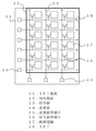
図3は、アクティブマトリックス型液晶表示装置を模式的に表した平面図である。アクティブマトリックス型液晶表示装置は、TFT基板11と対向基板12との間に液晶層を挟持させた構造を有している。TFT基板11には、信号線13と走査線14の交差部に画素電極17がマトリックス状に配設され、各画素電極17には駆動用のTFT(スイッチング素子)18が付設されている。信号線13の端部には信号線用端子16が設けられており、また走査線14の端部には走査線用端子15が設けられている。これら信号線端子16および走査線端子15は、フレキシブル配線基板の端子や駆動回路などのバンプの圧着、また表示検査時の駆動信号入力のためのプローブの接触等をする電気接続用端子である。一方、対向基板12には図示はしていないが共通電極やカラーフイルタおよび配向膜が設けられている。なお、共通電極は、TFT基板上に設けるものもある。
【0004】
図4(a)〜(f)は、液晶表示装置の製造方法、特にTFT基板の製造方法の1例を工程順に示した断面図である。ガラスなどの透明基板21上に第1のメタル層を形成し、パターニングして走査線22および走査線用端子23を形成する。この上全面に第1の絶縁膜24を形成する。次に全面に第2のメタル層を形成し、パターニングして信号線25および信号線用端子26を形成する。次にこれらの上全面に第2の絶縁層27を形成する。次にコンタクトホール28および29を形成して走査線用端子23および信号線用端子26を露出させる。次にこの上全面に透明な導電膜を形成し、パターニングして画素電極30および走査線用端子と信号線用端子に接続された透明電極31、32を形成する。この後、表示領域に配向膜を形成する。この後、配向膜上に液晶分子を所定方向に配列させるために、例えばラビングなどによりある方向性をもった傷を形成する。なお、スイッチング素子であるTFTの形成工程については、本発明に直接関係がないので省略してある。
【0005】
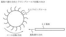
ラビングは、図5に示すようにラビングロール51を回転させながら基板52の表面をスライドさせ、ラビング布の毛で配向膜上にある方向性をもった傷を形成する方法が一般的である。このラビング方法によると、ラビング布の毛により削られた配向膜屑や、ラビング布から剥離した繊維屑といったゴミが発生する。またラビング工程ではあるまとまった枚数の基板をまとめて処理するため、ラビングロールに付着する等したゴミは一基板のみならず、処理する基板全体に運ばれることになる。こうやって運ばれたゴミは、コンタクトホール等、基板上の表面段差の大きい部分に多く付着する。
【0006】
ここで、ラビングによる段差へのゴミ付着例を図6に示す。図5に示すようなラビングロール51の回転,基板進行方向の場合、図6に示すように基板52に形成されている段差部53のA部およびB部に屑が付着する。この回転方向であるとラビング方向前方のB部の屑はラビングロールの毛により掻きだされるためゴミの付着量が少ないが、ラビング方向後方のA部はラビングロールの回転方向に対して影になっているため、よりゴミの付着量が多くなる。よってラビング時のゴミ付着を軽減させる場合、このゴミの付着量が多いA部に相当する段差を軽減することにより、ゴミ付着量が大幅に軽減する。
【0007】
ここで従来の端子構造を説明する。第1の従来技術の端子構造を図7に示す。図7(a)は平面図であり、図7(b)はA−A断面図である。断面構造は、図7(b)に示すように基板10上より、第1のメタル層1、第1の絶縁膜6、第2のメタル層2、第2の絶縁膜7、ITO層3からなる。また、各層メタルの接続用として、第1のコンタクトホール4と、第2のコンタクトホール5が配置される。第1のコンタクトホール4により第1のメタル層1と第2のメタル層2が、第2のコンタクトホール5により第2のメタル層2とITO層3が接続される。平面構造は、図7(a)に示すように外側からITO層3、第1のメタル層1、第2のメタル層2、第1のコンタクトホール4、第2のコンタクトホール5と順に形成される。
【0008】
また第1の従来技術より工程数を削減した場合の端子構造として、第2の従来技術の端子構造を説明する。第2の従来技術を図8に示す。図8(a)は平面図であり、図8(b)はB−B断面図である。断面構造は、図8(b)に示すように基板10上より、第1のメタル層1、第1の絶縁膜6、第2の絶縁膜7、ITO層3からなる。また、第1のメタル層1とITO膜3との接続用として、第1のコンタクトホール4が配置される。第1のコンタクトホール4は第1の絶縁膜6と第2の絶縁膜7の両膜にホールを形成する。平面構造は、図8(a)に示すように外側からITO層3、第1のメタル層1、第1のコンタクトホール4、と順に形成される。これら従来の端子構造は、第1のコンタクトホール4と第2のコンタクトホール5の端面が近接もしくは一致しているため、最上層のITO層3の表面段差は第1の絶縁膜6、第2の絶縁膜7の厚みをあわせた分とほぼ同等であり大きい。よって先に述べたラビング工程でのゴミが付着量は多くなる。
【0009】
なお、この配向膜の屑付着を軽減させるための技術として、従来基板表面の段差を軽減することによりゴミ付着防止や配向膜の印刷性の向上する方法が提案されている。この方法は、スイッチング素子と画素電極とを電気的に接続するためのコンタクトホール内に有機樹脂の平坦化層を設けるというものである(特許文献1参照)。
【0010】
また、他の従来の技術として、表示領域外にダミー電極を配列し、ラビング処理時布材から剥離した繊維屑をダミー電極で除去することで表示領域内にゴミが進入するのを防ぐことが提案されている(特許文献2参照)。
【0011】
【特許文献1】
特開2001−311963号公報(〔0029〕、〔0030〕、図1)
【特許文献2】
特開平9−43629号公報(〔0007〕〜〔0010〕、図1)
【0012】
【発明が解決しようとする課題】
上記した第1の従来の端子構造の場合、第1のコンタクトホール4と第2のコンタクトホール5の端面が近接しているため、最上層のITO層3の表面段差は第1の絶縁膜6、第2の絶縁膜7の厚みをあわせた分とほぼ同等であり大きい。また段差を軽減するため第1のコンタクトホール4の端面に対して第2のコンタクトホール5の端面を所定の間隔以上離すように形成すれば一段差の変化量が小さくなりゴミ付着量は軽減できるが、第2のコンタクトホール5のサイズがかなり小さくなり電気的接続においてコンタクト(接触)抵抗の増加が懸念される。
【0013】
また、第2の従来の端子構造の場合、第1のコンタクトホール4で第1の絶縁膜6、第2の絶縁膜7に同時に穴を形成するため、最上層のITO層3の表面段差は両層厚みをあわせた分となり、表面段差が大きくなる。このためゴミが付着し易いという問題がある。
【0014】
また、上記特許文献1の段差を軽減する方法は、コンタクトホール内に有機樹脂の平坦化層を形成するという方法であり、本発明が対象にしている端子部へ適用すると当然のことながら圧着する側との導通はとれなくなってしまう。
【0015】
さらに、上記特許文献2の段差を軽減する方法は、表示領域へのゴミ付着を対策するものであり、この技術により端子部のゴミ付着の軽減はできない。また、前記ダミー電極に相当するようなゴミを除去する何らかのパターンを端子部周辺に配置するには、それらのパターンを形成するためのスペースが必要である。設計的に余分なスペースがない場合には、この技術を使用することは難しい。
【0016】
本発明の目的は、こうした端子部における段差を、従来の特性を損なうことなく小さくできる電気接続用端子構造を有する液晶表示装置およびその製造方法を提供することである。
【0017】
【課題を解決するための手段】
本発明は、透明絶縁性基板上にマトリクス状に配置された複数の走査線と信号線を備え、走査線と信号線との交差部には画素電極およびスイッチング素子が設けられている第1の基板と、この第1の基板と平行に配置された第2の基板と、第1の基板と第2の基板との間に挟持された液晶とを有する液晶表示装置において、前記走査線および信号線の電気接続用端子部が、段差を小さくした構造を有することを特徴とする。電気接続用端子部は、第1のメタル層と、第1のメタル層を露出させるための第1のコンタクトホールを備える第1の絶縁膜と、前記第1のコンタクトホール内に前記第1のメタル層に接続するように形成した第2のメタル層と、前記第2のメタル層を露出させるための第2のコンタクトホールを備える第2の絶縁膜と、前記第2のメタル層と接続するように形成した透明電極層とから構成され、前記第2のコンタクトホールは、第1のコンタクトホールの外周壁より所定の間隔を開けて小さく形成されている。第2のコンタクトホールは、前記第1のコンタクトホールの中央にまたは前記第1のコンタクトホールの中央からラビング方向にずれて設けられている形成されている。透明電極層は、その端辺が前記第2の絶縁膜の段差のある外周壁より間隔をあけて小さく形成されていることを特徴とする。そして透明電極層は、その外周部が前記第2のコンタクトホール上から前記第2の絶縁膜の上に掛るように形成されている。前記透明電極層は、ラビング方向にずれた第2のコンタクトホール上に、前記第2のメタル層に接続されて設けられている。
【0018】
また、本発明によれば、透明基板上にメタル層を形成し、パターニングして走査線と共にその電気接続用端子部となる第1のメタル層を形成する工程と、この上全面に第1の絶縁膜を形成し前記第1のメタル層を露出させるための第1のコンタクトホールを形成する工程と、この上全面にメタル層を形成し、パターニングして信号線と共に前記第1のメタル層に接続された第2のメタル層を形成する工程と、これらの上全面に第2の絶縁層を形成し第2のコンタクトホールを設け前記第2のメタル層を露出させる工程と、この上全面に透明な導電膜を形成し、パターニングして画素電極および前記第2のメタル層に接続された透明電極層を形成する工程と、外周部の電気接続用端子部の部分を除いた全面(表示領域)に配向膜を形成する工程と、この配向膜上に液晶分子を所定方向に配列させるためのラビング処理を行う工程とを有する液晶表示装置の製造方法において、前記第2のコンタクトホールは、第1のコンタクトホールの外周壁より所定の間隔を開けて小さく形成されている液晶表示装置の製造方法が得られる。第2のコンタクトホールは、第1のコンタクトホールの中央部に位置するように形成されているか、または第2のコンタクトホールは、第1のコンタクトホールの内部でラビング方向にずれて形成されており、透明電極層は、第2のコンタクトホール上に形成されている。
【0019】
【発明の実施の形態】
次に本発明について図面を参照して詳細に説明する。ここではアクティブマトリックス型液晶表示装置を例にとって説明する。本発明の液晶表示装置の全体構成は、図3に模式的に示したように、TFT基板11と対向基板12との間に液晶層を挟持させた構造を有している。TFT基板11には、信号線13と走査線14の交差部に画素電極17がマトリクス状に配設され、各画素電極17には駆動用のTFT(スイッチング素子)18が付設されている。信号線13の端部には信号線用端子16が設けられており、また走査線14の端部には走査線用端子15が設けられている。これら信号線端子16および走査線端子15は、フレキシブル配線基板端子や駆動回路などのバンプの圧着、また表示検査時の駆動信号入力のためのプローブの接触等をする電気接続用端子である。一方、対向基板12には図示はしていないが共通電極やカラーフイルタおよび配向膜が設けられている。本発明の特徴部分は、以下に説明するように信号線端子および走査線端子の構造にある。
【0020】
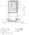
図1(a)、(b)は、本発明の第1の実施形態である走査線端子または信号線端子構造を示す平面図および断面図である。端子の断面構造は、図1(b)に示すようにガラスなどの透明基板10上に設けた第1のメタル層1、この第1のメタル層1を露出させるための第1のコンタクトホール4を形成した第1の絶縁膜6、第1のメタル層1と接続するように第1のコンタクトホール4内に設けた第2のメタル層2、この第2のメタル層2を露出させるための第2のコンタクトホール5を備える第2の絶縁膜7、第2のコンタクトホール5を介して第2のメタル層2と接続するように設けたITO層3からなる。ITO層3は、その外周部が第2のコンタクトホール5の上から第2の絶縁膜7に掛かるように形成されている。
【0021】
平面構造は、図1(a)に示すように第2のコンタクトホール5は、第1のコンタクトホール4の外周壁より所定の間隔をあけて小さく形成されている。ITO層3は、圧着する側の導電パターンの外形,ピッチ等にあわせて形成され、その内側に第2のコンタクトホール5が配置される。すなわち、ITO層3は、第2のコンタクトホール5より広い幅aを有しており、外周部は第2の絶縁膜7の上まで延びて形成されている。しかしITO層3の外周幅は、第1のメタル層1、第1のコンタクトホール4および第2のメタル層2の端辺の幅より小さくされている。ITO層3の外周辺は、第1のメタル層1、第1のコンタクトホール4および第2のメタル層2の端辺とは所定の間隔をあけて配置されている。ここでいう所定の間隔とは、第1のコンタクトホール4により形成される段差と、第2のコンタクトホール5により形成される段差の位置を離すためのものである。なお、ITO層3の少なくとも1辺において、第1のメタル層1、第1のコンタクトホール4および第2のメタル層2の端辺と所定の間隔をあけて配置されておればよい。
【0022】
次に本発明の液晶表示装置の製造方法、特に図1に示す端子構造を有するTFT基板の製造方法の1例を工程順に説明する。ガラスなどの透明基板の上に、メタル層を形成し、パターニングして例えば走査線と共にその端子部となる第1のメタル層1を形成する。つぎにこの上全面に第1の絶縁膜6を形成し、第1のコンタクトホール4を設けて端子部の第1のメタル層1を露出させる。ついで第1の絶縁膜6の上にメタル層を形成し、パターニングして例えば信号線と共に第1のコンタクトホール4内に第1のメタル層1と接続された第2のメタル層2を形成する。つぎにこの上全面に第2の絶縁膜7を形成し、この第2の絶縁膜7に第1のコンタクトホール4より小さい第2のコンタクトホール5を形成し、第2のメタル層2の1部を露出させる。つぎにこの上全面にITO膜を設け、パターニングして画素電極と共に第2のコンタクトホール5の上にITO層3を形成する。このITO層3は、第2のコンタクトホール5より大きいが第1のコンタクトホール4より小さい広がりを有するように形成する。この後、外周部の走査線用端子と信号線用端子の部分などを除いた表示領域に配向膜を形成し、配向膜表面に液晶分子を所定方向に配列させるために、例えばラビングなどによりある方向性をもった傷を形成する。
【0023】
なお、スイッチング素子であるTFTの形成工程については、本発明に直接関係がないので省略してある。また、対向基板は従来と同様に透明基板上に共通電極やカラーフイルタおよび配向膜を形成して製作する。このようにして製作したTFT基板と、べつに製作した対向基板とを間に液晶層を挟んで対向させることにより液晶表示装置が完成する。なお、ここでは対向基板上に共通電極を設ける例について述べたが、共通電極はTFT基板側に設けてもよい。
【0024】
このように本実施形態の電気接続用端子においては、端子を構成しているITO層3の表面の段差が第2の絶縁膜7の厚みのみとなるため、表面段差は小さくなりラビング工程において端子へのゴミ付着を軽減できるという効果がある。
【0025】
次に本発明の第2の実施形態の端子構造について説明する。図2(a)、(b)は、本発明の第2の実施形態である電気接続用端子を示す断面図および平面図である。断面構造は図2(b)に示すように、透明基板10上に形成した第1のメタル層1、この第1のメタル層1の上部に形成した第1のコンタクトホール4を有する第1の絶縁膜6、第1のコンタクトホール4内に第1のメタル層1と接続するように形成した第2のメタル層2、第2のコンタクトホール5を有する第2の絶縁膜7、第2のコンタクトホール5を介して第2のメタル層2に接続されたITO層3からなる。ここで第2のコンタクトホール5は、第1のコンタクトホール4の中央からラビング方向に偏って設けられている。ITO層3は、偏ったコンタクトホール5の上に外周部が第2の絶縁膜7に掛かるように設けられている。
【0026】
平面構造は、図2(a)に示すようにITO層3が圧着する側の端子の外形,ピッチにあわせて形成され、その内側に第2のコンタクトホール5が配置される。そして第1のメタル層1、第1のコンタクトホール4、第2のメタル層2の端辺が、ITO層3の一部の端辺に対して所定の間隔をあけて形成されている。すなわちITO層3がラビング方向に偏って形成されており、ラビング方向の後方部では第1のコンタクトホール4の端辺に対し間隔があいている。これは図6で説明したことから分かるように、ラビング方向の前端部(B部)にはラビング時の配向膜の屑がたまりにくいが、後端部(A部)では屑がたまりやすいので、本実施形態のようにラビング方向の後方部において、端子のITO層が段差を形成している第1のコンタクトホール4の端辺から間隔があいて離れておれば、端子へのゴミ付着は少ないからである。ここが第1の実施形態との相違点になる。この第2の実施形態の端子構造は、上述した第1の実施形態とほぼ同様の工程を経て製作することができる。
【0027】
この第2の実施形態によれば、第1のメタル層1、第1のコンタクトホール4、第2のメタル層2の形成領域を第1の実施形態よりも小さくできるため、圧着側の端子ピッチが狭い場合等でも活用でき、屑の発生状況によっては第1の実施形態と同等の効果が期待できる。
【0028】
【発明の効果】
以上詳細に述べたように、本発明の電気接続用端子構造によれば、以下のような効果が得られる。
(1)外部と電気接触する領域a(図1参照)の表面段差が小さくなり、ラビング時の配向膜屑やラビング布から剥離した繊維屑に代表されるような工程上で発生するゴミが端子へ付着することを軽減できる。
(2)領域a(図2参照)を広げる必要がないため、圧着側の端子が狭ピッチの場合にも活用できる。
(3)第1のコンタクトホール、第2のコンタクトホールとも広く形成することが可能であり、コンタクト抵抗の低減が可能である。
【図面の簡単な説明】
【図1】(a)、(b)は、本発明の第1の実施形態である端子構造を示す平面図および断面図である。
【図2】(a)、(b)は、本発明の第2の実施形態である端子構造を示す平面図および断面図である。
【図3】アクティブマトリックス型液晶表示装置の構成を模式的に示した平面図である。
【図4】液晶表示装置の製造工程の要部を工程順に説明する断面図である。
【図5】基板のラビング工程を説明するための図である。
【図6】基板のラビング工程において、基板の段差部にゴミが付着する様子を説明するための図である。
【図7】(a)、(b)は、従来の端子構造を示す平面図および断面図である。
【図8】(a)、(b)は、従来の他の端子構造を示す平面図および断面図である。
【符号の説明】
1 第1のメタル層
2 第2のメタル層
3 ITO層
4 第1のコンタクトホール
5 第2のコンタクトホール
6、24 第1の絶縁膜
7、27 第2の絶縁膜
10、21 基板
11 TFT基板
12 対向基板
13、25 信号線
14、22 走査線
15、23 走査線用端子
16、26 信号線用端子
17、30 画素電極
28、29 コンタクトホール
31、32 透明電極
51 ラビングロール
52 基板
53 段差部[0001]
TECHNICAL FIELD OF THE INVENTION
The present invention relates to a liquid crystal display device and a method of manufacturing the same, and more particularly, to a liquid crystal display device having a structure capable of reducing adhesion of dust to an electric connection terminal portion formed on a substrate of a liquid crystal display panel and a method of manufacturing the same.
[0002]
[Prior art]
Liquid crystal display devices are widely used as displays for personal computers and TVs. Among them, an active matrix type liquid crystal display device has a high-speed response, is suitable for increasing the number of pixels, and has been put to practical use as a display for realizing a high-quality, large-sized, and color display screen. Hereinafter, an active matrix type liquid crystal display device will be described as an example.
[0003]
FIG. 3 is a plan view schematically showing an active matrix type liquid crystal display device. The active matrix type liquid crystal display device has a structure in which a liquid crystal layer is sandwiched between a
[0004]
FIGS. 4A to 4F are cross-sectional views illustrating an example of a method of manufacturing a liquid crystal display device, in particular, a method of manufacturing a TFT substrate in the order of steps. A first metal layer is formed on a transparent substrate 21 such as glass and patterned to form a
[0005]
The rubbing is generally performed by sliding the surface of the
[0006]
Here, an example of dust adhering to a step due to rubbing is shown in FIG. In the case of the rotation of the rubbing roll 51 and the traveling direction of the substrate as shown in FIG. 5, debris adheres to the portions A and B of the step portion 53 formed on the
[0007]
Here, a conventional terminal structure will be described. FIG. 7 shows a first prior art terminal structure. FIG. 7A is a plan view, and FIG. 7B is an AA cross-sectional view. As shown in FIG. 7B, the cross-sectional structure is from the
[0008]
Also, a terminal structure according to the second prior art will be described as a terminal structure in a case where the number of steps is reduced as compared with the first prior art. FIG. 8 shows a second conventional technique. FIG. 8A is a plan view, and FIG. 8B is a BB cross-sectional view. The cross-sectional structure includes a
[0009]
As a technique for reducing the adhesion of dust on the alignment film, there has been proposed a method for preventing dust adhesion and improving the printability of the alignment film by reducing steps on the substrate surface. In this method, a flattening layer of an organic resin is provided in a contact hole for electrically connecting a switching element and a pixel electrode (see Patent Document 1).
[0010]
Further, as another conventional technique, dummy electrodes are arranged outside the display area, and fiber dust separated from the cloth material during the rubbing process is removed by the dummy electrode to prevent dust from entering the display area. It has been proposed (see Patent Document 2).
[0011]
[Patent Document 1]
JP 2001-319663 A ([0029], [0030], FIG. 1)
[Patent Document 2]
JP-A-9-43629 ([0007] to [0010], FIG. 1)
[0012]
[Problems to be solved by the invention]
In the case of the first conventional terminal structure described above, since the end surfaces of the
[0013]
In the case of the second conventional terminal structure, holes are formed in the first insulating film 6 and the second
[0014]
Further, the method of reducing the level difference in
[0015]
Further, the method of reducing the level difference described in
[0016]
An object of the present invention is to provide a liquid crystal display device having an electric connection terminal structure capable of reducing such a step in a terminal portion without deteriorating the conventional characteristics, and a method of manufacturing the same.
[0017]
[Means for Solving the Problems]
The first aspect of the present invention includes a plurality of scanning lines and signal lines arranged in a matrix on a transparent insulating substrate, and a pixel electrode and a switching element are provided at intersections of the scanning lines and the signal lines. In a liquid crystal display device having a substrate, a second substrate arranged in parallel with the first substrate, and a liquid crystal sandwiched between the first substrate and the second substrate, the scanning lines and the signal The electric connection terminal portion of the wire has a structure in which a step is reduced. The electrical connection terminal portion includes a first metal layer, a first insulating film including a first contact hole for exposing the first metal layer, and a first insulating film provided in the first contact hole. A second metal layer formed so as to be connected to the metal layer, a second insulating film having a second contact hole for exposing the second metal layer, and a connection to the second metal layer The second contact hole is formed smaller at a predetermined interval from the outer peripheral wall of the first contact hole. The second contact hole is formed so as to be provided at the center of the first contact hole or shifted from the center of the first contact hole in the rubbing direction. The transparent electrode layer is characterized in that its edge is formed smaller at a distance from the stepped outer peripheral wall of the second insulating film. The transparent electrode layer is formed so that its outer peripheral portion extends from above the second contact hole to above the second insulating film. The transparent electrode layer is provided on the second contact hole shifted in the rubbing direction and connected to the second metal layer.
[0018]
Further, according to the present invention, a step of forming a metal layer on a transparent substrate and patterning the same to form a first metal layer to be an electric connection terminal portion together with a scanning line, Forming an insulating film and forming a first contact hole for exposing the first metal layer, forming a metal layer on the entire surface of the first contact hole, and patterning the metal layer together with a signal line in the first metal layer; Forming a connected second metal layer, forming a second insulating layer on the entire upper surface thereof, providing a second contact hole, and exposing the second metal layer; A step of forming a transparent conductive film and patterning to form a transparent electrode layer connected to the pixel electrode and the second metal layer; Forming an alignment film Performing a rubbing process for arranging liquid crystal molecules in a predetermined direction on the alignment film, wherein the second contact hole is formed at a predetermined distance from an outer peripheral wall of the first contact hole. Thus, a method of manufacturing a liquid crystal display device which is formed small with an interval therebetween can be obtained. The second contact hole is formed so as to be located at the center of the first contact hole, or the second contact hole is formed so as to be shifted in the rubbing direction inside the first contact hole. The transparent electrode layer is formed on the second contact hole.
[0019]
BEST MODE FOR CARRYING OUT THE INVENTION
Next, the present invention will be described in detail with reference to the drawings. Here, an active matrix type liquid crystal display device will be described as an example. The overall configuration of the liquid crystal display device of the present invention has a structure in which a liquid crystal layer is sandwiched between a
[0020]
FIGS. 1A and 1B are a plan view and a cross-sectional view illustrating a scanning line terminal or signal line terminal structure according to a first embodiment of the present invention. As shown in FIG. 1B, the sectional structure of the terminal is a
[0021]
In the planar structure, as shown in FIG. 1A, the
[0022]
Next, an example of a method of manufacturing the liquid crystal display device of the present invention, in particular, an example of a method of manufacturing a TFT substrate having the terminal structure shown in FIG. A metal layer is formed on a transparent substrate such as glass and patterned to form, for example, a
[0023]
The step of forming the TFT as a switching element is omitted because it is not directly related to the present invention. The counter substrate is manufactured by forming a common electrode, a color filter, and an alignment film on a transparent substrate as in the related art. The liquid crystal display device is completed by facing the TFT substrate manufactured in this manner and the counter substrate manufactured separately with a liquid crystal layer interposed therebetween. Although the example in which the common electrode is provided over the counter substrate is described here, the common electrode may be provided on the TFT substrate side.
[0024]
As described above, in the electrical connection terminal of the present embodiment, the step on the surface of the
[0025]
Next, a terminal structure according to a second embodiment of the present invention will be described. FIGS. 2A and 2B are a cross-sectional view and a plan view showing an electric connection terminal according to a second embodiment of the present invention. As shown in FIG. 2B, the cross-sectional structure has a
[0026]
The planar structure is formed according to the outer shape and pitch of the terminal on the side where the
[0027]
According to the second embodiment, the formation area of the
[0028]
【The invention's effect】
As described in detail above, according to the terminal structure for electrical connection of the present invention, the following effects can be obtained.
(1) The surface step of the region a (see FIG. 1) that is in electrical contact with the outside is reduced, and dust generated in a process typified by alignment film dust at the time of rubbing or fiber dust peeled from the rubbing cloth is generated by the terminal Can be reduced.
(2) Since it is not necessary to expand the area a (see FIG. 2), it can be utilized even when the terminals on the crimp side have a narrow pitch.
(3) Both the first contact hole and the second contact hole can be formed widely, and the contact resistance can be reduced.
[Brief description of the drawings]
FIGS. 1A and 1B are a plan view and a cross-sectional view showing a terminal structure according to a first embodiment of the present invention.
FIGS. 2A and 2B are a plan view and a cross-sectional view illustrating a terminal structure according to a second embodiment of the present invention.
FIG. 3 is a plan view schematically showing a configuration of an active matrix type liquid crystal display device.
FIG. 4 is a cross-sectional view for explaining main parts of a manufacturing process of the liquid crystal display device in order of process.
FIG. 5 is a view for explaining a rubbing step of the substrate.
FIG. 6 is a view for explaining how dust adheres to a step portion of the substrate in a rubbing step of the substrate.
FIGS. 7A and 7B are a plan view and a sectional view showing a conventional terminal structure.
FIGS. 8A and 8B are a plan view and a cross-sectional view showing another conventional terminal structure.
[Explanation of symbols]
DESCRIPTION OF
Claims (11)
Priority Applications (5)
| Application Number | Priority Date | Filing Date | Title |
|---|---|---|---|
| JP2003149482A JP4517063B2 (en) | 2003-05-27 | 2003-05-27 | Liquid crystal display |
| US10/848,716 US7142276B2 (en) | 2003-05-27 | 2004-05-19 | LCD device having a smaller level difference |
| TW093114913A TWI248545B (en) | 2003-05-27 | 2004-05-26 | LCD device having a smaller level difference |
| KR1020040037819A KR100649915B1 (en) | 2003-05-27 | 2004-05-27 | Lcd device having a smaller level difference |
| CN2004100474201A CN1573477B (en) | 2003-05-27 | 2004-05-27 | LCD device having a smaller level difference |
Applications Claiming Priority (1)
| Application Number | Priority Date | Filing Date | Title |
|---|---|---|---|
| JP2003149482A JP4517063B2 (en) | 2003-05-27 | 2003-05-27 | Liquid crystal display |
Publications (2)
| Publication Number | Publication Date |
|---|---|
| JP2004354496A true JP2004354496A (en) | 2004-12-16 |
| JP4517063B2 JP4517063B2 (en) | 2010-08-04 |
Family
ID=33447691
Family Applications (1)
| Application Number | Title | Priority Date | Filing Date |
|---|---|---|---|
| JP2003149482A Expired - Lifetime JP4517063B2 (en) | 2003-05-27 | 2003-05-27 | Liquid crystal display |
Country Status (5)
| Country | Link |
|---|---|
| US (1) | US7142276B2 (en) |
| JP (1) | JP4517063B2 (en) |
| KR (1) | KR100649915B1 (en) |
| CN (1) | CN1573477B (en) |
| TW (1) | TWI248545B (en) |
Cited By (1)
| Publication number | Priority date | Publication date | Assignee | Title |
|---|---|---|---|---|
| WO2013073495A1 (en) * | 2011-11-18 | 2013-05-23 | シャープ株式会社 | Active matrix substrate, liquid crystal display device and method for manufacturing active matrix substrate |
Families Citing this family (6)
| Publication number | Priority date | Publication date | Assignee | Title |
|---|---|---|---|---|
| JP2007108470A (en) * | 2005-10-14 | 2007-04-26 | Nec Lcd Technologies Ltd | Active matrix substrate and liquid crystal display device |
| JP5019834B2 (en) * | 2006-09-26 | 2012-09-05 | インフォビジョン オプトエレクトロニクス ホールデングズ リミティッド | Display device substrate and display device |
| US8218116B2 (en) * | 2007-08-01 | 2012-07-10 | Sony Corporation | Liquid crystal display panel and manufacturing method thereof |
| JP5154298B2 (en) * | 2007-08-01 | 2013-02-27 | 株式会社ジャパンディスプレイウェスト | Liquid crystal display panel and manufacturing method thereof |
| CN105824162B (en) * | 2016-06-01 | 2020-09-01 | 北京京东方光电科技有限公司 | Array substrate, manufacturing method thereof and display device |
| CN109581718A (en) * | 2019-01-30 | 2019-04-05 | 京东方科技集团股份有限公司 | Array substrate mother matrix, array substrate, display panel and display device |
Citations (7)
| Publication number | Priority date | Publication date | Assignee | Title |
|---|---|---|---|---|
| JPH09171197A (en) * | 1995-11-21 | 1997-06-30 | Samsung Electron Co Ltd | Manufacture of liquid crystal display device |
| JPH09230362A (en) * | 1996-02-20 | 1997-09-05 | Semiconductor Energy Lab Co Ltd | Liquid crystal display device |
| JPH1115022A (en) * | 1997-06-26 | 1999-01-22 | Nec Corp | Liquid crystal display device and manufacturing method therefor |
| JPH11242238A (en) * | 1997-12-26 | 1999-09-07 | Sharp Corp | Reflection type liquid crystal display device, manufacture therefor and manufacture of circuit board |
| JP2001194679A (en) * | 2000-01-13 | 2001-07-19 | Seiko Epson Corp | Liquid crystal device and its manufacturing method |
| JP2002207223A (en) * | 2000-10-31 | 2002-07-26 | Sharp Corp | Method for manufacturing display device, and substrate for display device |
| JP2004094020A (en) * | 2002-09-02 | 2004-03-25 | Toshiba Matsushita Display Technology Co Ltd | Liquid crystal display |
Family Cites Families (6)
| Publication number | Priority date | Publication date | Assignee | Title |
|---|---|---|---|---|
| JPH0943629A (en) | 1995-07-31 | 1997-02-14 | Sony Corp | Liquid crystal display device |
| KR100660809B1 (en) | 1999-12-31 | 2006-12-26 | 엘지.필립스 엘시디 주식회사 | Liquid crystal display device and method for fabricating the same |
| JP2001311963A (en) | 2000-04-27 | 2001-11-09 | Toshiba Corp | Liquid crystal display device and manufacturing method therefor |
| JP4815659B2 (en) * | 2000-06-09 | 2011-11-16 | ソニー株式会社 | Liquid crystal display |
| KR100685945B1 (en) * | 2000-12-29 | 2007-02-23 | 엘지.필립스 엘시디 주식회사 | Liquid crystal display and manufacturing method of the same |
| KR100858297B1 (en) * | 2001-11-02 | 2008-09-11 | 삼성전자주식회사 | Reflective-transmissive type liquid crystal display device and method of manufacturing the same |
-
2003
- 2003-05-27 JP JP2003149482A patent/JP4517063B2/en not_active Expired - Lifetime
-
2004
- 2004-05-19 US US10/848,716 patent/US7142276B2/en active Active
- 2004-05-26 TW TW093114913A patent/TWI248545B/en active
- 2004-05-27 KR KR1020040037819A patent/KR100649915B1/en active IP Right Grant
- 2004-05-27 CN CN2004100474201A patent/CN1573477B/en active Active
Patent Citations (7)
| Publication number | Priority date | Publication date | Assignee | Title |
|---|---|---|---|---|
| JPH09171197A (en) * | 1995-11-21 | 1997-06-30 | Samsung Electron Co Ltd | Manufacture of liquid crystal display device |
| JPH09230362A (en) * | 1996-02-20 | 1997-09-05 | Semiconductor Energy Lab Co Ltd | Liquid crystal display device |
| JPH1115022A (en) * | 1997-06-26 | 1999-01-22 | Nec Corp | Liquid crystal display device and manufacturing method therefor |
| JPH11242238A (en) * | 1997-12-26 | 1999-09-07 | Sharp Corp | Reflection type liquid crystal display device, manufacture therefor and manufacture of circuit board |
| JP2001194679A (en) * | 2000-01-13 | 2001-07-19 | Seiko Epson Corp | Liquid crystal device and its manufacturing method |
| JP2002207223A (en) * | 2000-10-31 | 2002-07-26 | Sharp Corp | Method for manufacturing display device, and substrate for display device |
| JP2004094020A (en) * | 2002-09-02 | 2004-03-25 | Toshiba Matsushita Display Technology Co Ltd | Liquid crystal display |
Cited By (3)
| Publication number | Priority date | Publication date | Assignee | Title |
|---|---|---|---|---|
| WO2013073495A1 (en) * | 2011-11-18 | 2013-05-23 | シャープ株式会社 | Active matrix substrate, liquid crystal display device and method for manufacturing active matrix substrate |
| JPWO2013073495A1 (en) * | 2011-11-18 | 2015-04-02 | シャープ株式会社 | Active matrix substrate, liquid crystal display device, and method of manufacturing active matrix substrate |
| US9164341B2 (en) | 2011-11-18 | 2015-10-20 | Sharp Kabushiki Kaisha | Active matrix substrate, liquid crystal display device and method for manufacturing active matrix substrate |
Also Published As
| Publication number | Publication date |
|---|---|
| US20040239857A1 (en) | 2004-12-02 |
| KR20040102344A (en) | 2004-12-04 |
| US7142276B2 (en) | 2006-11-28 |
| TW200510882A (en) | 2005-03-16 |
| TWI248545B (en) | 2006-02-01 |
| JP4517063B2 (en) | 2010-08-04 |
| CN1573477B (en) | 2010-05-26 |
| CN1573477A (en) | 2005-02-02 |
| KR100649915B1 (en) | 2006-11-24 |
Similar Documents
| Publication | Publication Date | Title |
|---|---|---|
| JP4004672B2 (en) | Substrate for liquid crystal display device and manufacturing method thereof | |
| CN100465715C (en) | Method for forming pad electrode, method for manufacturing liquid crystal display device | |
| KR101192073B1 (en) | Fringe Field Switching mode Liquid Crystal Display device and fabrication method thereof | |
| US9057905B2 (en) | Touch sensor, manufacturing method thereof, and liquid crystal display having touch panel | |
| TWI297095B (en) | Bonding pad structure for a display and fabrication method thereof | |
| JP4442684B2 (en) | Liquid crystal display device and manufacturing method thereof | |
| KR20070000893A (en) | Liquid crystal display apparatus of horizontal electronic field applying type and fabricating method thereof | |
| TWI512582B (en) | Touch panel and touch display panel | |
| JP2011118429A (en) | Display panel | |
| US8633069B2 (en) | Array substrate and manufacturing method thereof, active display | |
| CN111554696A (en) | Total reflection type display substrate, manufacturing method thereof and total emission type display device | |
| CN111638616B (en) | Display substrate and manufacturing method thereof, display panel and manufacturing method thereof | |
| JP2002116712A (en) | Display device and its manufacturing method | |
| JP2004354496A (en) | Liquid crystal display device and method for manufacturing the same | |
| KR101832270B1 (en) | Liquid crystal display device and method of fabricating thereof | |
| CN105974689A (en) | Array substrate and preparation method thereof and liquid crystal display panel | |
| US20100078644A1 (en) | Insulating film pattern, method for manufacturing the same, and method for manufacturing thin film transistor substrate using the same | |
| JPH10161149A (en) | Manufacture of array substrate for display device | |
| US8040477B2 (en) | Array substrate, liquid crystal display panel, and method of manufacturing the same | |
| KR20120075111A (en) | Fringe field switching liquid crystal display device and method of fabricating the same | |
| JP4842709B2 (en) | Manufacturing method of display device | |
| JP2009271105A (en) | Method for manufacturing liquid crystal display device | |
| JP4850589B2 (en) | Display device | |
| CN112596316B (en) | Array substrate and preparation method thereof, display panel and preparation method thereof, and display device | |
| KR20090073709A (en) | Method of fabricating color filter on tft type array substrate for in-plane switching mode liquid crystal display device |
Legal Events
| Date | Code | Title | Description |
|---|---|---|---|
| RD01 | Notification of change of attorney |
Free format text: JAPANESE INTERMEDIATE CODE: A7421 Effective date: 20050317 |
|
| A621 | Written request for application examination |
Free format text: JAPANESE INTERMEDIATE CODE: A621 Effective date: 20060417 |
|
| RD01 | Notification of change of attorney |
Free format text: JAPANESE INTERMEDIATE CODE: A7421 Effective date: 20070126 |
|
| RD01 | Notification of change of attorney |
Free format text: JAPANESE INTERMEDIATE CODE: A7421 Effective date: 20080618 |
|
| A977 | Report on retrieval |
Free format text: JAPANESE INTERMEDIATE CODE: A971007 Effective date: 20090113 |
|
| RD01 | Notification of change of attorney |
Free format text: JAPANESE INTERMEDIATE CODE: A7421 Effective date: 20090602 |
|
| A131 | Notification of reasons for refusal |
Free format text: JAPANESE INTERMEDIATE CODE: A131 Effective date: 20090804 |
|
| A521 | Request for written amendment filed |
Free format text: JAPANESE INTERMEDIATE CODE: A523 Effective date: 20090918 |
|
| A131 | Notification of reasons for refusal |
Free format text: JAPANESE INTERMEDIATE CODE: A131 Effective date: 20091104 |
|
| A521 | Request for written amendment filed |
Free format text: JAPANESE INTERMEDIATE CODE: A523 Effective date: 20100104 |
|
| TRDD | Decision of grant or rejection written | ||
| A711 | Notification of change in applicant |
Free format text: JAPANESE INTERMEDIATE CODE: A711 Effective date: 20100312 |
|
| A01 | Written decision to grant a patent or to grant a registration (utility model) |
Free format text: JAPANESE INTERMEDIATE CODE: A01 Effective date: 20100316 |
|
| A01 | Written decision to grant a patent or to grant a registration (utility model) |
Free format text: JAPANESE INTERMEDIATE CODE: A01 |
|
| A61 | First payment of annual fees (during grant procedure) |
Free format text: JAPANESE INTERMEDIATE CODE: A61 Effective date: 20100405 |
|
| FPAY | Renewal fee payment (event date is renewal date of database) |
Free format text: PAYMENT UNTIL: 20130528 Year of fee payment: 3 |
|
| R150 | Certificate of patent or registration of utility model |
Ref document number: 4517063 Country of ref document: JP Free format text: JAPANESE INTERMEDIATE CODE: R150 Free format text: JAPANESE INTERMEDIATE CODE: R150 |
|
| FPAY | Renewal fee payment (event date is renewal date of database) |
Free format text: PAYMENT UNTIL: 20130528 Year of fee payment: 3 |
|
| S111 | Request for change of ownership or part of ownership |
Free format text: JAPANESE INTERMEDIATE CODE: R313113 |
|
| FPAY | Renewal fee payment (event date is renewal date of database) |
Free format text: PAYMENT UNTIL: 20130528 Year of fee payment: 3 |
|
| R350 | Written notification of registration of transfer |
Free format text: JAPANESE INTERMEDIATE CODE: R350 |
|
| FPAY | Renewal fee payment (event date is renewal date of database) |
Free format text: PAYMENT UNTIL: 20130528 Year of fee payment: 3 |
|
| R250 | Receipt of annual fees |
Free format text: JAPANESE INTERMEDIATE CODE: R250 |
|
| R250 | Receipt of annual fees |
Free format text: JAPANESE INTERMEDIATE CODE: R250 |
|
| R250 | Receipt of annual fees |
Free format text: JAPANESE INTERMEDIATE CODE: R250 |
|
| R250 | Receipt of annual fees |
Free format text: JAPANESE INTERMEDIATE CODE: R250 |
|
| R250 | Receipt of annual fees |
Free format text: JAPANESE INTERMEDIATE CODE: R250 |
|
| R250 | Receipt of annual fees |
Free format text: JAPANESE INTERMEDIATE CODE: R250 |
|
| R250 | Receipt of annual fees |
Free format text: JAPANESE INTERMEDIATE CODE: R250 |
|
| R250 | Receipt of annual fees |
Free format text: JAPANESE INTERMEDIATE CODE: R250 |
|
| R250 | Receipt of annual fees |
Free format text: JAPANESE INTERMEDIATE CODE: R250 |
|
| R250 | Receipt of annual fees |
Free format text: JAPANESE INTERMEDIATE CODE: R250 |
|
| S111 | Request for change of ownership or part of ownership |
Free format text: JAPANESE INTERMEDIATE CODE: R313113 |
|
| R350 | Written notification of registration of transfer |
Free format text: JAPANESE INTERMEDIATE CODE: R350 |
|
| EXPY | Cancellation because of completion of term | ||
| RD02 | Notification of acceptance of power of attorney |
Free format text: JAPANESE INTERMEDIATE CODE: R3D02 |