【0001】
【発明の属する技術分野】
本発明は、陽極と陰極との間に有機EL材料からなる異なるピーク波長の発光を行う複数の発光層を含む有機層を挟持してなる有機EL(エレクトロルミネッセンス)素子に関し、特に、白色発光を行う有機EL素子に用いて好適である。
【0002】
【従来の技術】
有機EL素子は自己発光のため、視認性に優れ、かつ数V〜数十Vの低電圧駆動が可能なため駆動回路を含めた軽量化が可能である。そこで、有機EL素子は、薄膜型ディスプレイ、照明、バックライトとしての活用が期待されている。
【0003】
また、有機EL素子は色バリエーションが豊富であることも特徴である。また、複数の発光色を組み合わせる混色によってさまざまな発光が可能となることも特徴である。
【0004】
発光色の中で、特に白色発光のニーズは高い。白色発光は車載ディスプレイの主流であり、またバックライトとしても活用できる。さらに、カラーフィルタを用いて青、緑、赤の画素に分けることが可能である。
【0005】
このような白色発光を行う有機EL素子としては、短波長発光である青色発光層と長波長発光である赤色発光層との2層を積層することにより、両発光層の混色として白色の発光を得るようにしたものが提案されている(例えば、特許文献1参照)。
【0006】
【特許文献1】
特開平7−142169号公報
【0007】
【発明が解決しようとする課題】
しかしながら、このような発色の異なる(つまり、異なるピーク波長の)2層の発光層を積層したものにおいては、素子の駆動時間すなわち発光時間や印加電圧の変化に伴って、2つの発光層において膜質が変化したり、正孔(ホール)や電子の輸送性の度合が変化する等により、発光中心が移動し、その結果、色度変化を生じやすい。
【0008】
特に、2つの発光層の混色として白色を得る場合、白色は他の色に比べて色度変化に敏感であるため、上記問題が顕在化する。
【0009】
そこで、本発明は上記問題に鑑み、異なるピーク波長を有する複数の発光層からの混色発光を行うようにした有機EL素子において、駆動時間や電圧変化に伴う色度変化を極力抑制できるようにすることを目的とする。
【0010】
【課題を解決するための手段】
上記目的を達成するため、本発明者らは鋭意検討を行い、図3(a)、(b)、(c)に示すような推定メカニズムを考えた。
【0011】
まず、従来の2層の発光層によって混色を得る場合について図3(a)に示す。図3(a)において、正孔輸送層H1と電子輸送層E1との間に二つの発光層AとBが積層されている場合を考える。ここで、一方の発光層Aを赤色側である長波長発光層A、他方の発光層Bを青色側である短波長発光層Bとする。
【0012】
そして、図3(a)に示すように、正孔hは正孔輸送層H1から長波長発光層A、短波長発光層Bへと移動し、電子eは電子輸送層E1から短波長発光層B、長波長発光層Aへと移動し、両発光層A、Bの界面を中心とした領域すなわち発光帯域R1にて発光が行われる。
【0013】
理想的には、この発光帯域R1にて発光すれば、両発光層A、Bの混色として所望の色度すなわち白色発光が得られる。しかし、駆動時間や電圧変化に伴う発光中心の移動によって、発光帯域も一方の発光層の側へ片寄り、発光帯域R1からR2へと移動する。
【0014】
この発光帯域の移動に伴い、例えば、図3(a)では、長波長発光層Aにおける発光の割合が増加し、短波長発光層Bにおける発光の割合が減少する。すると、理想である白色に対して、赤色がかった発色となってしまう。
【0015】
そこで、異なるピーク波長の発光を行う発光層を交互に積層する場合に、従来の2層発光層の構成に対して、発光層の数を増加させることを考えた。例えば、図3(b)に示すように、発光層を3層構成とした場合には、次のような効果が推測される。
【0016】
図3(b)では、発光層を長波長発光層A、短波長発光層B、長波長発光層Aの3層としている。この場合、理想的な白色発光を実現する発光帯域R1から、発光帯域が移動して発光帯域R2になったとしても、図に示すように、長波長発光層Aと短波長発光層Bの発光に占める割合は実質的に変化しないため、色度変化もほとんどないと考えられる。
【0017】
そして、異なるピーク波長の発光を行う発光層を交互に積層するにあたって発光層を4層以上の積層構成とした場合にも、図3(b)に示す場合と同様の考えから、発光帯域が移動したとしても、2層発光層の場合に比べて、色度変化を抑制できると考えられる。
【0018】
しかしながら、実際には、図3(c)に示すように、長波長発光層Aと短波長発光層Bのホスト材料のポテンシャルエネルギー準位が一般に異なるため、発光帯域R1を十分に広げることが困難である場合が生じることがわかった。そのような場合には、発光層を3層構成とした場合でも、2層発光層の場合と同様な現象が生じ、色度変化の抑制効果が十分でなくなってしまう。
【0019】
このような問題の発生原因としては、従来の2層構成の発光層の例をみてみると次のような理由が考えられる。従来の2層発光層では、正孔輸送層側の発光層はそのホストが正孔輸送性物質であり、電子輸送層側の発光層はそのホストが電子輸送性物質である。
【0020】
このようなホストの構成では、積層された各発光層は、正孔が移動しやすい発光層と電子が移動しやすい発光層とに分けられた形となる。そのため、上記図3(a)に示したように、エネルギーギャップを有する両発光層の界面付近にて正孔と電子とが再結合し、両発光層が発光する形となっている。
【0021】
このような2層発光層における発光形態を考えると、3層構成の発光層においても同様の現象が起こると考えられる。つまり、ある発光層と他の発光層との間では正孔や電子の移動が不十分となり、3層の発光層のうち、ある2層の界面にて発光が生じやすくなることが考えられる。そのため、上記図3(b)に示したような3層に渡る広い発光帯域R1の実現が困難になると考えられる。
【0022】
そこで、本発明者らは、3層以上の発光層とした場合において、各発光層の間でエネルギーギャップが存在したとしても、正孔や電子がすべての各発光層間を移動しやすくすればよいのではないかと考えた。
【0023】
そして、積層するすべての発光層において、ホストとして正孔輸送性物質と電子輸送性物質との混合物を用いれば、各発光層において、正孔輸送機能および電子輸送機能が十分に発揮されると考え、実験検討を行った。本発明は、この検討結果に基づいて創出されたものである。
【0024】
すなわち、請求項1に記載の発明では、陽極(20)、正孔輸送層(40)、発光層(50)、電子輸送層(60)および陰極(70)を備える有機EL素子において、前記発光層(50)は、異なるピーク波長の発光を行う発光層(51、52、53、54、55)が交互に3層以上積層されたものであり、かつ、これら積層された各々の発光層は、ドーパントと、ホストとしての正孔輸送性物質および電子輸送性物質とを含んでなるものであることを特徴とする。
【0025】
本発明は、実験的に見出されたものであり、発光層(50)を、異なるピーク波長の発光を行う発光層(51、52、53、54、55)が交互に3層以上積層されたものとした場合に、各々の発光層を、ドーパントと、ホストとしての正孔輸送性物質および電子輸送性物質とを含んでなるものとすれば、従来に比べて駆動時間や電圧変化に伴う色度変化を極力抑制することができる。
【0026】
ここで、請求項2に記載の発明のように、前記積層された各々の発光層(51〜55)のすべてにおいて、ホストが同じ物質からなることが好ましい。
【0027】
それによれば、各発光層(51〜55)のエネルギー準位を同程度にすることができ、各発光層(51〜55)の間のエネルギーギャップを極力小さくできるので、発光帯域をより広いものとできる。
【0028】
また、請求項3に記載の発明のように、前記発光層(50)は、前記積層された各々の発光層(51〜55)の発光の混色として白色の発光を行うものにできる。
【0029】
また、請求項4に記載の発明では、前記発光層(50)中の前記正孔輸送性物質が、前記正孔輸送層(40)中の物質と同じであることを特徴とする。
【0030】
それによれば、発光層(50)中の正孔輸送性物質が正孔輸送層(40)中の物質と同じであるため、正孔輸送層(40)から発光層(50)への正孔の注入を容易にしてその効率を向上させることができるとともに、材料を兼用することでコスト低減を図ることができる。
【0031】
さらに、請求項5に記載の発明では、前記発光層(50)中の前記電子輸送性物質が、前記電子輸送層(60)中の物質と同じであることを特徴とする。
【0032】
それによれば、発光層(50)中の電子輸送性物質が電子輸送層(60)中の物質と同じであるため、電子輸送層(60)から発光層(50)への電子の注入を容易にしてその効率を向上させることができるとともに、材料を兼用することでコスト低減を図ることができる。
【0033】
請求項6に記載の発明では、前記発光層(50)中の前記正孔輸送性物質が前記正孔輸送層(40)中の物質と同じであり、且つ、前記発光層中の前記電子輸送性物質が前記電子輸送層(60)中の物質と同じであることを特徴とする。
【0034】
それによれば、上記請求項4および請求項5に記載の発明と同様の効果を奏することができる。
【0035】
また、請求項7に記載の発明では、前記積層された各々の発光層(51〜55)のホストにおいて、前記正孔輸送性物質の割合が1重量%〜30重量%であることを特徴とする。また、請求項8に記載の発明では、前記積層された各々の発光層(51〜55)のホストにおいて、前記電子輸送性物質の割合が99重量%〜70重量%であることを特徴とする。
【0036】
これら請求項7および請求項8に記載の発明は、積層された各発光層(51〜55)のホストにおいて、正孔輸送性物質の割合及び電子輸送性物質の割合を限定したものである。これにより、移動度の高い正孔と移動度の低い電子との発光層(50)中におけるバランスをとり、効率の向上及び耐久性の向上を図ることができる。
【0037】
請求項9に記載の発明では、前記発光層(50)中の前記正孔輸送性物質および前記電子輸送性物質のガラス転移温度が、120℃以上であることを特徴とする。
【0038】
それによれば、発光層(50)中の正孔輸送性物質と電子輸送性物質のガラス転移温度が120℃以上であるため、高温での耐久性向上のためには好ましい。
【0039】
ところで、陽極(20)と正孔輸送層(40)との間に正孔注入層(30)を設ける場合、銅フタロシアニン(以下、「CuPc」と略記する)からなるものが好ましい。このCuPcは分子内の分極が大きいため、陽極(20)との密着性が高いためである。
【0040】
高温下での安定性を向上させるには、陽極(20)との界面の密着性を向上させることは重要である。そこで、陽極(20)と接する正孔注入層(30)としては、形態変化の小さいポルフィリン系化合物層を設けることが好ましい。
【0041】
本発明者らは、陽極(20)と接する正孔注入層(30)としてポルフィリン系化合物であるCuPcを採用した場合について、そのCuPc膜の結晶状態の変化に着目した。
【0042】
その結果、高温環境下の放置前後で、このCuPc膜の結晶状態が大きく異なることを見出した。このCuPc膜の結晶状態の変化について、具体的に調べた結果を示す。
【0043】
この結晶状態における変化の確認は効率良く行うため、放置環境温度を120℃と高くして加速し、放置時間は2時間で評価することとした。以下、この条件における放置を加速高温放置という。
【0044】
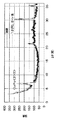
ガラス基板上に、ITO(インジウム−スズの酸化物)からなる陽極を形成し、アルゴンと酸素混合のプラズマによる表面処理を陽極表面に施した後、陽極上にCuPcを成膜した。この場合におけるCuPc膜の結晶の状態を、上記加速高温放置の前と後でX線回折によって分析した結果を図2に示す。
【0045】
図2に示すように、回折ピークにおいて、2θ=6.68°に発生しているピークがCuPcの結晶構造に由来している。図2では、このピークにおいて実線で図示するものが加速高温放置の前のピークすなわち初期のピークであり、破線で図示するものが加速高温放置の後のピークすなわち120℃、2時間放置後のピークである。
【0046】
そして、このピーク値の積分値が大きい、すなわちピーク値が高いほど、CuPc膜の結晶性が高いことを示している。図2では、120℃、2時間の加速高温放置によって、当該ピーク値(積分値)が加速高温放置前の1.5倍に変化している。
【0047】
このことから、本発明者らは、結晶性正孔注入層であるCuPc膜上に正孔輸送層、発光層、電子輸送層、陰極等が成膜された後、つまり、発光素子形態になってから、CuPc膜がこのような結晶状態の変化を起こすことが、CuPc膜の密着性の低下を引き起こす原因であると考えた。
【0048】
つまり、CuPc膜の結晶性ができるだけ高くなるように成膜すれば、CuPc膜の密着性、特に、陽極との界面の密着性を向上させることができると考えた。
【0049】
そして、鋭意検討の結果、請求項10に記載の発明のように、前記陽極(20)と前記正孔輸送層(40)との間に、CuPcからなる正孔注入層(30)を設けた場合、CuPcのX線回折法により現れる回折ピークの値において、有機EL素子の使用温度内の加熱による回折ピークの変化量が、前記加熱前の回折ピークの±25%以内となっているものであれば、よいことがわかった。
【0050】
このように、正孔注入層(30)としてのCuPc膜の高温環境下における結晶状態の変化を小さくすれば、CuPc膜の密着性を向上できる。その結果、高温での耐久性向上に有利となる。また、温度変化により生じるCuPc膜の凹凸を極力低減し、ショートやリークの発生を抑制できる。
【0051】
なお、上記各手段の括弧内の符号は、後述する実施形態に記載の具体的手段との対応関係を示す一例である。
【0052】
【発明の実施の形態】
本実施形態における有機EL素子は、陽極、正孔輸送層、発光層、電子輸送層および陰極を備えるものであり、必要に応じて、陽極と正孔輸送層との間に正孔注入層を設けたり、電子輸送層と陰極との間に電子注入層を設けてもよい。
【0053】
ここで、発光層は、異なるピーク波長の発光を行う発光層が交互に3層以上積層されたものであり、かつ、これら各々の発光層は、ドーパントとホストとしての正孔輸送性物質および電子輸送性物質とを含んでなるものである。
【0054】
なお、異なるピーク波長の発光を行う発光層が交互に3層以上積層されたものとは、比較的長いピーク波長の発光を行う発光層と比較的短いピーク波長の発光を行う発光層とが交互に3層以上積層されたものである。つまり、長波長発光層と短波長発光層とが交互に3層以上積層されたものである。
【0055】
また、正孔輸送性物質とは、所定の電界下で電子の移動度よりも正孔の移動度の方が大きいものをいい、電子輸送性物質とは、所定の電界下で正孔の移動度よりも電子の移動度の方が大きいものをいう。
【0056】
この有機EL素子の基本動作は、周知のとおり、本質的に、電子及び正孔を電極から注入する過程と、電子及び正孔が固体中を移動する過程と、電子及び正孔が再結合し、一重項又は三重項励起子を生成する過程と、その励起子が発光する過程とからなる。
【0057】
本実施形態の有機EL素子につき、さらに説明する。図1は本発明の実施形態に係る有機EL素子S1の概略断面構成を示す図である。
【0058】
図1中、10は基板であり、通常、ソーダガラス、バリウムシリケートガラス、アルミノシリケートガラスなどのガラスか、ポリエステル、ポリカーボネート、ポリスルホン、ポリメチルメタクリレート、ポリプロピレン、ポリエチレンなどのプラスチック、石英、陶器などのセラミックをはじめとする汎用の基板材料を板状、シート状又はフィルム状に形成して用いられ、必要に応じて、これらは適宜積層して用いられる。
【0059】
望ましい基板材料は透明なガラス及びプラスチックであり、シリコンなどの不透明なセラミックは、透明な電極と組合せて用いられる。発光の色度を調節する必要があるときには、基板10の適所に、例えば、フィルター膜、色度変換膜、誘電体反射膜などの色度調節手段を設ける。
【0060】
20は陽極であり、電気的に低抵抗率であって、しかも、全可視領域にわたって光透過率の大きい金属若しくは電導性化合物の1または複数を、例えば、真空蒸着、スパッタリング、化学蒸着(CVD)、原子層エピタクシー(ALE)、塗布、浸漬などの方法により、基板10の一側に密着させてなる。
【0061】
ここで、陽極20は、この陽極20における抵抗率が1kΩ/□以下、望ましくは、5〜50Ω/□になるように、厚さ10〜1000nm、望ましくは、50〜500nmの単層または多層に成膜することによって形成される。
【0062】
陽極20における電導性材料としては、例えば、金、白金、銀、銅、コバルト、ニッケル、パラジウム、バナジウム、タングステン、アルミニウムなどの金属、酸化亜鉛、酸化錫、酸化インジウム、酸化錫と酸化インジウムとの混合系(以下、「ITO」と略記する)などの金属酸化物、さらには、アニリン、チオフェン、ピロールなどを反復単位とする電導性オリゴマー及び電導性ポリマーが挙げられる。
【0063】
このうち、ITOは、低抵抗率のものが容易に得られるうえに、酸などを用いてエッチングすることにより、微細パターンを容易に形成できる特徴がある。
【0064】
30は正孔注入層であり、通常、陽極20におけると同様の方法により、陽極20に密着させて、正孔注入性物質を厚さ1〜100nmに成膜することによって形成される。
【0065】
正孔注入性物質としては、陽極20からの正孔注入と輸送を容易ならしめるべく、イオン化電位が小さく、かつ、例えば、104〜106V/cmの電界下において、少なくとも、10−6cm2/V・秒の正孔移動度を発揮するものが望ましい。個々の正孔注入性物質としては、有機EL素子において汎用される、例えば、フタロシアニン誘導体、特に銅フタロシアニンが最も好ましい。
【0066】
40は正孔輸送層であり、通常、陽極20におけると同様の方法により、正孔注入層30に密着させて、正孔輸送性物質を厚さ1〜100nmに成膜することによって形成される。
【0067】
個々の正孔輸送性物質としては、有機EL素子において汎用される、例えば、アリールアミン誘導体、イミダゾール誘導体、オキサジアゾール誘導体、オキサゾール誘導体、トリアゾール誘導体、カルコン誘導体、スチリルアントラセン誘導体、スチルベン誘導体、テトラアリールエテン誘導体、トリアリールアミン誘導体、トリアリールエテン誘導体、トリアリールメタン誘導体、フタロシアニン誘導体、フルオレノン誘導体、ヒドラゾン誘導体、N−ビニルカルバゾール誘導体、ピラゾリン誘導体、ピラゾロン誘導体、フェニルアントラセン誘導体、フェニレンジアミン誘導体、ポリアリールアルカン誘導体、ポリシラン誘導体、ポリフェニレンビニレン誘導体などが挙げられ、必要に応じて、これらは適宜組合せて用いられる。
【0068】
また、分子内の分極が大きく、陽極20すなわちITO等との密着性が高い化合物は、正孔注入性物質あるいは、正孔注入/輸送層性物質としても用いることができる。
【0069】
50は発光層であり、本例では、異なるピーク波長の発光を行う発光層51、52、53、54、55が交互に5層積層されたものである。そして、積層された各々の発光層51〜55は、ドーパントと、ホストとしての正孔輸送性物質および電子輸送性物質からなる混合物とを含んでなるものである。
【0070】
発光層50は、通常、陽極20におけると同様の方法により、正孔輸送層40に密着させて、発光層1層の厚さをそれぞれ1nm〜100nmに成膜することによって形成される。
【0071】
具体的には、各発光層51〜55は、共蒸着法により形成されるものであり、実際には、各発光層51〜55の界面では、隣り合う発光層51〜55の材料同士が混合された層を形成している場合もある。
【0072】
ここで、各発光層51〜55におけるドーパントとしては、有機EL素子において汎用される蛍光色素材料を用いることができる。そのような蛍光色素材料としては、例えば、青色系の発光を行うペリレン、黄色系の発光を行うルブレン、緑色系の発光を行うクマリン等が挙げられる。
【0073】
また、各発光層51〜55におけるホストの正孔輸送性物質としては、上記正孔輸送層40に用いられる正孔輸送性物質から選択された物質を用いることができる。また、各発光層51〜55におけるホストの電子輸送性物質としては、後述の電子輸送層60に用いられる電子輸送性物質から選択された物質を用いることができる。
【0074】
このようなホストの正孔輸送性物質としては、例えば、トリフェニルアミン4量体等が挙げられ、ホストの電子輸送性物質としては、例えば、トリピレニルアダマンタン、トリス(8−キノリノラート)アルミニウム(以下、「Alq3」という)等が挙げられる。
【0075】
また、発光層50においては、積層された各々の発光層51〜55のすべてにおいて、ホストが同じ物質からなることが好ましい。例えば、5層の発光層51〜55のすべてにおいて、ホストがトリフェニルアミン4量体とトリピレニルアダマンタンとの混合物からなるようにすることが好ましい。
【0076】
また、発光層50のホストとしての正孔輸送性物質が、正孔輸送層40中の物質と同じであることが好ましい。そのようにすれば、正孔輸送層40から発光層50への正孔の注入を容易にしてその効率を向上させることができるとともに、材料を兼用することで有機EL素子のコスト低減を図ることができる。
【0077】
また、発光層50のホストとしての電子輸送性物質が、発光層50の上に位置する電子輸送層60中の物質と同じであることが好ましい。そのようにすれば、電子輸送層60から発光層50への電子の注入を容易にしてその効率を向上させることができるとともに、材料を兼用することで有機EL素子のコスト低減を図ることができる。
【0078】
また、発光層50において、積層された各発光層51〜55のホストにおける正孔輸送性物質と電子輸送性物質の割合は、ホストからの発光が生じない限り特に限定されないが、混合物の状態で所期の機能を有効に作用するのに好ましい割合は、正孔輸送性物質が1重量%〜90重量%、電子輸送性物質が99重量%〜10重量%であり、さらに望ましくは,正孔輸送性物質が1重量%〜30重量%、電子輸送性物質が99重量%〜70重量%である。
【0079】
この割合は、移動度の高い正孔と移動度の低い電子との発光層50中におけるバランスをとったもので、この割合を外れると混合ホストとしての機能が有効に作用しない場合が生じ、ホスト材料からの発光が観測され、輝度寿命の低下が大きくなる。
【0080】
また、発光層50において、積層された各発光層51〜55におけるドーパントは、ホスト材料全体に対して、0.05〜50重量%、望ましくは、0.1〜30重量%の割合とすることができる。
【0081】
また、高温での耐久性向上のためには、発光層50中の正孔輸送性物質および電子輸送性物質のガラス転移温度が、120℃以上であることが好ましい。
【0082】
次に、図1において、発光層50の上に位置する上記電子輸送層60は、通常、陽極20におけると同様の方法により、発光層50に密着させて、電子親和力の大きい有機化合物を1つまたは複数を厚さ10〜100nmに成膜することによって形成される。
【0083】
複数の電子輸送性物質を用いる場合には、その複数の電子輸送性物質を均一に混合して単層に形成しても、混合することなく、電子輸送性物質ごとに隣接する複数の層に形成してもよい。
【0084】
好ましい電子輸送性物質はキノリノール金属錯体、ベンゾキノン、アントラキノン、フルオレノンなどの環状ケトン又はその誘導体、シラザン誘導体であり、この中でもキノリノール金属錯体が最も好ましい。
【0085】
ここでいうキノリノール金属錯体とは、分子内にピリジン残基とヒドロキシ基とを有する、例えば、8−キノリノール類、ベンゾキノリン−10−オール類などの配位子としてのキノリノール類と、そのピリジン残基における窒素原子から電子対の供与を受けて配位子と配位結合を形成する、中心原子としての、例えば、リチウム、ベリリウム、マグネシウム、カルシウム、亜鉛、アルミニウム、ガリウム、インジウムなどの周期律表における第1族、第2族、第12族又は第13族に属する金属若しくはその酸化物からなる錯体一般を意味する。
【0086】
配位子が8−キノリノール類又はベンゾキノリン−10−オールのいずれかである場合、それらは置換基を1又は複数有していてもよく、ヒドロキシ基が結合する8位または10位の炭素以外の炭素へ、例えば、フルオロ基、クロロ基、ブロモ基、ヨード基などのハロゲン基、メチル基、トリフルオロメチル基、エチル基、プロピル基、イソプロピル基、ブチル基、イソブチル基、sec−ブチル基、tert−ブチル基、ペンチル基、イソペンチル基、ネオペンチル基、tert−ペンチル基などの脂肪族炭化水素基、メトキシ基、トリフルオロメトキシ基、エトキシ基、プロポキシ基、イソプロポキシ基、ブトキシ基、イソブトキシ基、sec−ブトキシ基、tert−ブトキシ基、ペンチルオキシ基、イソペンチルオキシ基、フェノキシ基、ベンジルオキシ基などのエーテル基、アセトキシ基、トリフルオロアセトキシ基、ベンゾイルオキシ基、メトキシカルボニル基、トリフルオロメトキシカルボニル基、エトキシカルボニル基、プロポキシカルボニル基などのエステル基、さらには、シアノ基、ニトロ基、スルホ基などの置換基が1つまたは複数結合することを妨げない。キノリノール金属錯体が分子内に2以上の配位子を有する場合、それらの配位子は互いに同じものであっても異なるものであってもよい。
【0087】
具体的なキノリノール金属錯体としては、例えば、上記Alq3、トリス(3,4−ジメチル−8−キノリノラート)アルミニウム、トリス(4−メチル−8−キノリノラート)アルミニウム、トリス(4−メトキシ−8−キノリノラート)アルミニウム、トリス(4,5−ジメチル−8−キノリノラート)アルミニウム、トリス(4,6−ジメチル−8−キノリノラート)アルミニウム、トリス(5−クロロ−8−キノリノラート)アルミニウム、トリス(5−ブロモ−8−キノリノラート)アルミニウム、トリス(5,7−ジクロロ−8−キノリノラート)アルミニウム、トリス(5−シアノ−8−キノリノラート)アルミニウム、トリス(5−スルホニル−8−キノリノラート)アルミニウム、トリス(5−プロピル−8−キノリノラート)アルミニウム、ビス(2−メチル−8−キノリノラート)アルミニウムオキシドなどのアルミニウム錯体が挙げられる。
【0088】
また、亜鉛錯体としては、例えば、ビス(8−キノリノラート)亜鉛、ビス(2−メチル−8−キノリノラート)亜鉛、ビス(2,4−ジメチル−8−キノリノラート)亜鉛、ビス(2−メチル−5−クロロ−8−キノリノラート)亜鉛、ビス(2−メチル−5−シアノ−8−キノリノラート)亜鉛、ビス(3,4−ジメチル−8−キノリノラート)亜鉛、ビス(4,6−ジメチル−8−キノリノラート)亜鉛、ビス(5−クロロ−8−キノリノラート)亜鉛、ビス(5,7−ジクロロ−8−キノリノラート)亜鉛などが挙げられる。
【0089】
さらに、ベリリウム錯体としては、例えば、ビス(8−キノリノラート)ベリリウム、ビス(2−メチル−8−キノリノラート)ベリリウム、ビス(2,4−ジメチル−8−キノリノラート)ベリリウム、ビス(2−メチル−5−クロロ−8−キノリノラート)ベリリウム、ビス(2−メチル−5−シアノ−8−キノリノラート)ベリリウム、ビス(3,4−ジメチル−8−キノリノラート)ベリリウム、ビス(4,6−ジメチル−8−キノリノラート)ベリリウム、ビス(5−クロロ−8−キノリノラート)ベリリウム、ビス(5,7−ジクロロ−8−キノリノラート)ベリリウム、ビス(10−ヒドロキシベンゾ[h]キノリノラート)ベリリウムなどが挙げられる。
【0090】
上記以外のキノリノール金属錯体としては、例えば、ビス(8−キノリノラート)マグネシウム、ビス(2−メチル−8−キノリノラート)マグネシウム、ビス(2,4−ジメチル−8−キノリノラート)マグネシウム、ビス(2−メチル−5−クロロ−8−キノリノラート)マグネシウム、ビス(2−メチル−5−シアノ−8−キノリノラート)マグネシウム、ビス(3,4−ジメチル−8−キノリノラート)マグネシウム、ビス(4,6−ジメチル−8−キノリノラート)マグネシウム、ビス(5−クロロ−8−キノリノラート)マグネシウム、ビス(5,7−ジクロロ−8−キノリノラート)マグネシウムなどのマグネシウム錯体、トリス(8−キノリノラート)インジウムなどのインジウム錯体、トリス(5−クロロ−8−キノリノラート)ガリウムなどのガリウム錯体、ビス(5−クロロ−8−キノリノラート)カルシウムなどのカルシウム錯体などが挙げられる。なお、上記したキノリノール金属錯体は、必要に応じて、適宜組合せて用いられる。
【0091】
また、上記した電子輸送性物質は単なる例示であって、本実施形態で用いる電子輸送性物質は決してこれらに限定されてはならない。
【0092】
また、図1において、70は陰極であり、通常、電子輸送層60に密着させて、電子輸送層60において用いられる化合物より仕事関数の低い(通常、5eV以下)、例えば、リチウム、マグネシウム、カルシウム、ナトリウム、リチウム、銀、銅、アルミニウム、インジウムなどの金属若しくは金属酸化物又は電導性化合物を単独または組合せて蒸着することによって形成する。
【0093】
陰極70の厚みについては特に制限がなく、電導性、製造コスト、素子全体の厚み、光透過性などを勘案しながら、通常、抵抗率が1kΩ/□以下になるように、厚さ10nm以上、望ましくは、50〜500nmに設定される。
【0094】
なお、電子の陰極70から電子輸送層60への移動を容易ならしめるために、陽極20における同様の方法により、陰極70における電子輸送層60へ接する側に、例えば、弗化リチウム(LiF)、酸化リチウムなどのアルカリ金属化合物やアルカリ土類金属化合物による厚さ0.1〜2nmの薄膜を形成してもよい。
【0095】
また、陰極70と、有機化合物を含有する電子輸送層60との間の密着性を高めるために、必要に応じて、例えば、芳香族ジアミン化合物、キナクリドン化合物、ナフタセン化合物、有機シリコン化合物又は有機燐化合物を含んでなる界面層を設けてもよい。
【0096】
このように、本実施形態の有機EL素子S1は、基板10上に、陽極20、正孔輸送層40、発光層50、電子輸送層60、陰極70、さらに、必要に応じて、正孔注入層30を隣接する層と互いに密着させながら一体に形成することにより得ることができる。
【0097】
各層を形成するにあたっては、有機化合物の酸化や分解、さらには、酸素や水分の吸着などを最小限に抑えるべく、高真空下、詳細には、10−5Torr以下で一貫作業するのが望ましい。
【0098】
また、発光層50において、積層される各々の発光層51〜56を形成するにあたっては、あらかじめ、ホストとドーパントとを所定の割合で混合しておくか、あるいは、真空蒸着における両者の加熱速度を互いに独立して制御することによって、発光層50における両者の配合比を調節する。
【0099】
かくして形成された有機EL素子S1は、使用環境における劣化を最小限に抑えるべく、素子の一部又は全体を、例えば、不活性ガス雰囲気下で封止ガラスや金属キャップにより封止するか、あるいは、紫外線硬化樹脂などによる保護層で覆うのが望ましい。
【0100】
本実施形態の有機EL素子S1の使用方法について説明すると、この有機EL素子S1は、用途に応じて、比較的高電圧のパルス性電圧を間欠的に印加するか、あるいは、比較的低電圧の直流電圧(通常、3〜50V)を連続的に印加して駆動する。
【0101】
この有機EL素子S1は、陽極20の電位が陰極70の電位より高いときにのみ発光する。したがって、この有機EL素子S1へ印加する電圧は直流であっても交流であってもよく、印加する電圧の波形、周期も適宜のものとすればよい。
【0102】
交流を印加すると、この有機EL素子S1は、原理上、印加する交流の波形および周期に応じて輝度が増減したり点滅を繰返す。図1に示す有機EL素子S1の場合、陽極20と陰極70との間に電圧を印加すると、陽極20から注入された正孔が正孔注入層30、正孔輸送層40を経て発光層50へ、また、陰極70から注入された電子が電子輸送層60を経て発光層50へそれぞれ到達する。
【0103】
その結果、発光層50において、正孔と電子の再結合が起こり、それにより生じた励起状態のドーパントから目的とする色の発光が陽極20および基板10を透過して放出されることとなる。本例では、5層の発光層51〜55の混色としての発光が行われる。
【0104】
ところで、本実施形態では、発光層50を、異なるピーク波長の発光を行う発光層51、52、53、54、55が交互に3層以上(本例では5層)積層されたものとした場合に、各々の発光層51〜55を、ドーパントと、ホストとしての正孔輸送性物質および電子輸送性物質とを含んでなるものとしている。
【0105】
それによれば、3層以上の発光層とした場合において、積層するすべての発光層51〜55において、ホストとして正孔輸送性物質と電子輸送性物質との混合物を用いることで、各発光層51〜55において、正孔輸送機能および電子輸送機能が十分に発揮される。
【0106】
そのため、各発光層51〜55の間でエネルギーギャップが存在したとしても、正孔や電子がすべての各発光層51〜55間を移動しやすくすることができ、従来に比べて駆動時間や電圧変化に伴う色度変化を極力抑制することができる。
【0107】
また、本実施形態の好ましい形態では、積層された各々の発光層51〜55のすべてにおいて、ホストが同じ物質からなるものとしている。それによれば、各発光層51〜55のエネルギー準位を同程度にすることができ、各発光層51〜55の間のエネルギーギャップを極力小さくできるので、発光帯域をより広いものとできる。
【0108】
また、本実施形態では、発光層50として、ホスト材料からの発光を抑えるために、ホスト材料は正孔輸送性物質と電子輸送性物質とからなる混合層が用いられていることで、次のような効果も奏する。
【0109】
すなわち、正孔は正孔輸送性物質によりドーパントへ運ばれ、また電子は電子輸送性物質によりドーパントへ運ばれる。そのため、ホスト材料中の正孔輸送性物質と電子輸送性物質中へ同時に正孔と電子が注入されることが抑えられ、ホストに由来する発光が抑制され、その劣化抑制・耐久性向上が図れる。
【0110】
このように、本実施形態の有機EL素子S1は、耐久性に優れているうえに、発光効率が高く、その結果として、輝度が大きいので、発光体や、情報を視覚的に表示する情報表示機器において多種多様の用途を有する。
【0111】
この有機EL素子S1を光源とする発光体は、消費電力が小さいうえに、軽量なパネル状に構成することができるので、一般照明の光源に加えて、例えば、液晶素子、複写装置、印字装置、電子写真装置、コンピューター及びその応用機器、工業制御機器、電子計測器、分析機器、計器一般、通信機器、医療用電子計測機器、自動車を含む車輌、船舶、航空機、宇宙船などに搭載する機器、航空機の管制機器、インテリア、看板、標識などにおける省エネルギーにして省スペースな光源として有用である。
【0112】
また、この有機EL素子S1を、例えば、コンピューター、テレビジョン、ビデオ、ゲーム、時計、電話、カーナビゲーション、車載用マルチメーター、オシロスコープ、レーダー、ソナーなどの情報表示機器に用いる場合には、単独で用いるか、あるいは、緑色域、青色域、及び赤色域で発光する有機EL素子の組合せとしてフルカラー用のディスプレイなどに使用できる。
【0113】
この中でも、特に耐久性が要求される車載用途のディスプレイに使用した場合が最も本実施形態の有機EL素子S1の特徴を生かすことができる。駆動方式としては、汎用の単純マトリックス方式やアクティブマトリックス方式を適用できる。
【0114】
また、本実施形態の有機EL素子S1を自動車や車輌に搭載して使用する場合、高温環境(例えば70〜80℃程度)となることは避けられない。有機層のうちアモルファス性の有機層はガラス転移温度(Tg)以上になると結晶化して膜表面の凹凸が増大し、電流のリークが生じやすくなる。そこで、車載用とする場合には、素子における有機層全てのTgが120℃以上であることが好ましい。
【0115】
また、本実施形態の有機EL素子S1を、例えば、車載用のディスプレイ等に採用した場合においては、その使用温度は−40℃〜120℃程度のものである。
【0116】
このような使用温度において、高温環境下での安定性を向上させるには、正孔注入層30の密着性、特に、陽極20との界面の密着性を向上させる必要がある。これは、両者の線膨張係数の差が大きいためと考えられる。
【0117】
そこで、陽極20と接する正孔注入層30としては、形態変化の小さいポルフィリン系化合物層を設けることが好ましい。
【0118】
具体的には、ポルフィリン系化合物としてCuPcを用いた場合、CuPcのX線回折法により現れる回折ピークの値において、有機EL素子S1の使用温度内の加熱による回折ピーク変化量が、加熱前の回折ピークの±25%以内になっているものが好ましい。使用温度は、本例では−40〜120℃である。
【0119】
ここで、CuPcの回折ピークはCuPcの結晶性を示すもので、CuPcからなる正孔注入層30すなわちCuPc膜30をX線回折法により測定したとき、基板10と平行なCuPc膜30の(200)面の回折ピークである。具体的には、上記図2に示した2θ=6.68°に発生しているピークに相当するものであり、これを、以下、CuPc結晶性ピークという。
【0120】
そして、本実施形態では、このCuPc結晶性ピーク(2θ=6.68°)の値つまりピークの積分値において、有機EL素子S1の使用温度(−40℃〜120℃)内の加熱による当該CuPc結晶性ピークの変化量が、加熱前の当該CuPc結晶性ピークの値の±25%以内とすることが好ましい。
【0121】
このCuPc結晶性ピークの値の加熱前後における変化量を±25%以内に小さく抑えることにより、CuPc膜の密着性を向上させることができる。そして、高温環境下で使用しても、ショートやリークが発生しない程度にまで、有機材料の結晶状態の変化を小さくすることができる。
【0122】
ちなみに、上記図2に示したデータでは、加熱前のCuPc結晶性ピークの値に比べ、加熱後のCuPc結晶性ピークの値は1.5倍と大きく変化しており、ショートおよびリークが発生しやすくなっている。
【0123】
このような、CuPc結晶性ピークの値の加熱前後における変化量を±25%以内に小さく抑えたCuPc膜30は、例えば、下地である陽極20の表面を150℃で紫外線オゾン処理し、続いて、520℃の材料加熱温度にてCuPcを蒸着して成膜することにより実現可能である。
【0124】
そして、本実施形態において、このようなCuPc膜30とすれば、正孔注入層30の密着性を向上させ、より高温環境に適した有機EL素子S1を提供することができる。
【0125】
また、上述したように、素子を形成した後、高温環境下において、正孔注入層30の結晶性が変化しがたい特性を有することが重要である。そのため、図1において、陽極20の直上の結晶性材料を結晶性が高い安定した膜に成膜するためには、陽極20の表面粗度が重要となる。つまり、より平坦な方が結晶性の高い安定した膜が形成できる。
【0126】
本実施形態では、陽極20としてITOを使用した場合、具体的には、その平均表面粗さRaが2nm以下であり、10点平均表面粗さRzが20nm以下であることが望ましい。図1の実施形態において、例えば、ガラス基板10上に形成した陽極20としてのITOの表面を研磨してRaを約1nm以下、Rzを約10nmとすることができる。
【0127】
次に、本実施形態について、限定するものではないが、以下の実施例および比較例を参照して、より具体的に述べる。
【0128】
【実施例】
(実施例1)
ガラス基板10上に150nmの厚さのITOである陽極20をスパッタリング法により形成した。パターニング後、ITO表面を研磨し、表面を平坦にする。具体的には、その平均表面粗さRaが2nm以下であり、10点平均表面粗さRzが20nm以下であることが望ましい。本例では、ITOの表面を研磨してRaを約1nm以下、Rzを約10nmとしたものを使用した。
【0129】
その陽極20の上に正孔注入層30として、CuPC(銅フタロシアニン)を真空蒸着法により15nm形成した。さらに正孔輸送層40としてトリフェニルアミン4量体を真空蒸着法により40nm形成するした。
【0130】
そして、本例では、発光層50として、異なるピーク波長の発光を行う発光層が交互に3層積層されたものとした。ここで、各発光層のホストはいずれも、正孔輸送性物質であるトリフェニルアミン4量体と電子輸送性物質であるトリピレニルアダマンタンとの混合物とした。
【0131】
すなわち、まず、ホストとしてのトリフェニルアミン4量体24重量%およびトリピレニルアダマンタン74重量%の混合物とドーパントとしてのペリレン2重量%とからなる短波長発光層51を10nm形成し、そして、ホストとしてのトリフェニルアミン4量体23重量%およびトリピレニルアダマンタン72重量%の混合物とドーパントとしてのルブレン5重量%とからなる長波長発光層52を20nm形成し、最後に、ホストとしてのトリフェニルアミン4量体24重量%およびトリピレニルアダマンタン74重量%の混合物とドーパントとしてのペリレン2重量%とからなる短波長発光層53を10nm形成した。
【0132】
このように、本例では、正孔輸送層40の上に、短波長発光層51、長波長発光層52、短波長発光層53の3層が積層されてなる発光層50を形成した。
【0133】
さらに、電子輸送層60としてAlq3を20nm形成した。これら有機層を形成した後、陰極70としてLiFを0.5nm成膜し、その上にAlを100nm成膜した。
【0134】
こうして、白色発光素子としての有機EL素子を得た。本例では、積層された3層の発光層51〜53においてペリレンによる青色発光とルブレンによる黄色発光が行われ、これらの混色として白色発光を行う。この素子について、国際照明委員会(CIE)による色度座標における色度は、(0.32、0.34)であった。
【0135】
この素子を85℃、400Cd/m2で1/64デューティ駆動で発光し続けた時の輝度半減寿命は、1300時間であった。さらに、輝度半減時の色度は(0.33、0.35)であり、色度変化は非常に小さかった。
【0136】
(実施例2)
本例では、発光層50として、異なるピーク波長の発光を行う発光層が交互に5層積層されたものとした。ここで、各発光層51〜55のホストはいずれも、正孔輸送性物質であるトリフェニルアミン4量体と電子輸送性物質であるトリピレニルアダマンタンとの混合物とした。
【0137】
すなわち、まず、ホストとしてのトリフェニルアミン4量体24重量%およびトリピレニルアダマンタン74重量%の混合物とドーパントとしてのペリレン2重量%とからなる短波長発光層51を5nm形成し、そして、ホストとしてのトリフェニルアミン4量体23重量%およびトリピレニルアダマンタン72重量%の混合物とドーパントとしてのルブレン5重量%とからなる長波長発光層52を10nm形成し、さらに、ホストとしてのトリフェニルアミン4量体24重量%およびトリピレニルアダマンタン74重量%の混合物とドーパントとしてのペリレン2重量%とからなる短波長発光層53を5nm形成し、そして、ホストとしてのトリフェニルアミン4量体23重量%およびトリピレニルアダマンタン72重量%の混合物とドーパントとしてのルブレン5重量%とからなる長波長発光層54を10nm形成し、最後に、ホストとしてのトリフェニルアミン4量体24重量%およびトリピレニルアダマンタン74重量%の混合物とドーパントとしてのペリレン2重量%とからなる短波長発光層55を5nm形成した。
【0138】
この発光層50以外は上記実施例1と同様に素子を作製し、白色発光素子としての有機EL素子を得た。本例では、積層された5層の発光層51〜55においてペリレンによる青色発光とルブレンによる黄色発光が行われ、これらの混色として白色発光を行う。この素子について、国際照明委員会(CIE)による色度座標における色度は、(0.31、0.33)であった。
【0139】
この素子を85℃、400Cd/m2で1/64デューティ駆動で発光し続けた時の輝度半減寿命は、1500時間であった。さらに、輝度半減時の色度は(0.32、0.34)であり、色度変化は非常に小さかった。
【0140】
(比較例1)
発光層50として、まず、ホストとしてのトリフェニルアミン4量体95重量%とドーパントとしてのルブレン5重量%とからなる長波長発光層を5nm形成し、そして、ホストとしてのトリピレニルアダマンタン98重量%とドーパントとしてのペリレン2重量%とからなる長波長発光層を20nm形成した。
【0141】
この発光層50以外は上記実施例1と同様に素子を作製し、白色発光素子としての有機EL素子を得た。本例では、積層された2層の発光層においてペリレンによる青色発光とルブレンによる黄色発光が行われ、これらの混色として白色発光を行う。この素子について、国際照明委員会(CIE)による色度座標における色度は、(0.35、0.42)であった。
【0142】
この素子を85℃、400Cd/m2で1/64デューティ駆動で発光し続けた時の輝度半減寿命は、800時間であった。さらに、輝度半減時の色度は(0.39、0.47)であり、色度変化は上記実施例に比べて大きかった。
【0143】
(比較例2)
発光層50として、まず、ホストとしてのトリフェニルアミン4量体98重量%とドーパントとしてのペリレン2重量%とからなる短波長発光層を5nm形成し、そして、ホストとしてのトリフェニルアミン4量体95重量%とドーパントとしてのルブレン5重量%とからなる長波長発光層を5nm形成し、最後に、ホストとしてのトリピレニルアダマンタン98重量%とドーパントとしてのペリレン2重量%とからなる短波長発光層を10nm形成した。
【0144】
この発光層以外は上記実施例1と同様に素子を作製し、白色発光素子としての有機EL素子を得た。本例では、積層された3層の発光層においてペリレンによる青色発光とルブレンによる黄色発光が行われ、これらの混色として白色発光を行う。この素子について、国際照明委員会(CIE)による色度座標における色度は、(0.33、0.38)であった。
【0145】
この素子を85℃、400Cd/m2で1/64デューティ駆動で発光し続けた時の輝度半減寿命は、800時間であった。さらに、輝度半減時の色度は(0.36、0.42)であり、色度変化は上記実施例に比べて大きかった。
【0146】
このように、上記実施例における有機EL素子においては、比較例である従来の有機EL素子に比べて駆動時間や電圧変化に伴う色度変化を極力抑制することができた。
【図面の簡単な説明】
【図1】本発明の実施形態に係る有機EL素子の概略断面図である。
【図2】CuPc膜の結晶性の状態を加速高温放置の前と後でX線回折によって分析した結果を示す図である。
【図3】本発明者らの推定メカニズムを示す図である。
【符号の説明】
20…陽極、30…正孔注入層、40…正孔輸送層、50…発光層、51〜56…積層された発光層、60…電子輸送層、70…陰極。[0001]
TECHNICAL FIELD OF THE INVENTION
The present invention relates to an organic EL (electroluminescence) element in which an organic layer including a plurality of light emitting layers, each of which emits light having a different peak wavelength, made of an organic EL material is interposed between an anode and a cathode. It is suitable for use in an organic EL device to be performed.
[0002]
[Prior art]
Since the organic EL element is self-luminous, it has excellent visibility and can be driven at a low voltage of several V to several tens V, so that the weight including the driving circuit can be reduced. Thus, organic EL elements are expected to be used as thin-film displays, lighting, and backlights.
[0003]
Further, the organic EL element is characterized by abundant color variations. Another feature is that various colors can be emitted by mixing a plurality of emission colors.
[0004]
Among emission colors, the need for white emission is particularly high. White light emission is the mainstream of in-vehicle displays and can also be used as a backlight. Furthermore, it is possible to divide into blue, green, and red pixels using a color filter.
[0005]
As an organic EL element that emits such white light, by laminating two layers, a blue light emitting layer that emits short wavelength light and a red light emitting layer that emits long wavelength, white light is emitted as a mixed color of both light emitting layers. There has been proposed a device that obtains the information (for example, see Patent Document 1).
[0006]
[Patent Document 1]
JP-A-7-142169
[0007]
[Problems to be solved by the invention]
However, in the case where such two light emitting layers having different colors (that is, different peak wavelengths) are stacked, the film quality of the two light emitting layers is changed according to the change in the driving time of the element, that is, the light emitting time or the applied voltage. Changes, or the degree of transportability of holes or electrons changes, and so the emission center shifts, and as a result, chromaticity changes easily occur.
[0008]
In particular, when white is obtained as a mixed color of two light-emitting layers, the above problem becomes apparent because white is more sensitive to chromaticity change than other colors.
[0009]
In view of the above problems, the present invention is to minimize the change in chromaticity due to driving time and voltage change in an organic EL device that performs mixed color light emission from a plurality of light emitting layers having different peak wavelengths. The purpose is to:
[0010]
[Means for Solving the Problems]
In order to achieve the above object, the present inventors have conducted intensive studies and considered an estimation mechanism as shown in FIGS. 3 (a), 3 (b) and 3 (c).
[0011]
First, FIG. 3A shows a case where color mixing is obtained by a conventional two light emitting layers. In FIG. 3A, a case is considered where two light emitting layers A and B are stacked between the hole transport layer H1 and the electron transport layer E1. Here, one light emitting layer A is a long wavelength light emitting layer A on the red side, and the other light emitting layer B is a short wavelength light emitting layer B on the blue side.
[0012]
Then, as shown in FIG. 3A, the holes h move from the hole transport layer H1 to the long wavelength light emitting layer A and the short wavelength light emitting layer B, and the electrons e move from the electron transport layer E1 to the short wavelength light emitting layer. B, the light moves to the long-wavelength light-emitting layer A, and light is emitted in a region centered on the interface between the two light-emitting layers A and B, that is, in the light-emitting band R1.
[0013]
Ideally, if light is emitted in this emission band R1, a desired chromaticity, that is, white light emission as a mixed color of the two light-emitting layers A and B can be obtained. However, due to the movement of the emission center due to the drive time or the voltage change, the emission band also shifts toward one of the emission layers and moves from the emission band R1 to R2.
[0014]
With the shift of the light emission band, for example, in FIG. 3A, the ratio of light emission in the long wavelength light emitting layer A increases and the ratio of light emission in the short wavelength light emitting layer B decreases. Then, the color becomes reddish with respect to the ideal white.
[0015]
Therefore, when the light emitting layers that emit light of different peak wavelengths are alternately stacked, the number of light emitting layers was considered to be increased as compared with the configuration of the conventional two-layer light emitting layer. For example, as shown in FIG. 3B, when the light emitting layer has a three-layer structure, the following effects are presumed.
[0016]
In FIG. 3B, the light emitting layers are three layers of a long wavelength light emitting layer A, a short wavelength light emitting layer B, and a long wavelength light emitting layer A. In this case, even if the light emission band moves from the light emission band R1 that realizes ideal white light emission to the light emission band R2, the light emission of the long wavelength light emission layer A and the short wavelength light emission layer B as shown in the figure. Since the ratio of the chromaticity does not substantially change, it is considered that there is almost no change in chromaticity.
[0017]
When the light-emitting layers emitting light of different peak wavelengths are alternately stacked, the light-emitting band is shifted based on the same idea as that shown in FIG. Even so, it is considered that the change in chromaticity can be suppressed as compared with the case of the two-layer light emitting layer.
[0018]
However, in practice, as shown in FIG. 3C, since the potential energy levels of the host materials of the long wavelength light emitting layer A and the short wavelength light emitting layer B are generally different, it is difficult to sufficiently expand the light emission band R1. Was found to occur. In such a case, even when the light-emitting layer has a three-layer structure, the same phenomenon as in the case of the two-layer light-emitting layer occurs, and the effect of suppressing the change in chromaticity becomes insufficient.
[0019]
As a cause of such a problem, the following reason can be considered when an example of a conventional light emitting layer having a two-layer structure is considered. In the conventional two-layer light emitting layer, the host of the light emitting layer on the hole transport layer side is a hole transporting substance, and the host of the light emitting layer on the electron transporting layer side is an electron transporting substance.
[0020]
In such a configuration of the host, each of the stacked light-emitting layers is divided into a light-emitting layer in which holes easily move and a light-emitting layer in which electrons easily move. Therefore, as shown in FIG. 3A, holes and electrons are recombined near the interface between the two light emitting layers having an energy gap, and the two light emitting layers emit light.
[0021]
Considering the light emission mode in such a two-layer light-emitting layer, it is considered that the same phenomenon occurs in the light-emitting layer having a three-layer structure. That is, it is considered that holes and electrons do not sufficiently move between a certain light emitting layer and another light emitting layer, and light emission is likely to occur at an interface of a certain two layers among the three light emitting layers. Therefore, it is considered that it is difficult to realize a wide emission band R1 over three layers as shown in FIG.
[0022]
Therefore, the present inventors need to make it easy for holes and electrons to move between all the light-emitting layers even when there is an energy gap between the light-emitting layers in the case of three or more light-emitting layers. I thought it might be.
[0023]
It is considered that if a mixture of a hole-transporting substance and an electron-transporting substance is used as a host in all the light-emitting layers to be laminated, the hole-transporting function and the electron-transporting function are sufficiently exhibited in each light-emitting layer. An experimental study was conducted. The present invention has been created based on the results of this study.
[0024]
That is, according to the first aspect of the present invention, in the organic EL device including the anode (20), the hole transport layer (40), the light emitting layer (50), the electron transport layer (60), and the cathode (70), The layer (50) is formed by alternately stacking three or more light emitting layers (51, 52, 53, 54, 55) that emit light of different peak wavelengths, and each of the stacked light emitting layers is , A dopant, and a hole-transporting substance and an electron-transporting substance as hosts.
[0025]
The present invention has been found experimentally, and three or more light emitting layers (51, 52, 53, 54, 55) that emit light of different peak wavelengths are alternately laminated. If each light-emitting layer is composed of a dopant and a hole-transporting substance and an electron-transporting substance as a host, the light-emitting layer may be accompanied by a change in driving time or a change in voltage as compared with the related art. Chromaticity change can be suppressed as much as possible.
[0026]
Here, as in the second aspect of the present invention, it is preferable that the host is made of the same substance in all of the stacked light emitting layers (51 to 55).
[0027]
According to this, the energy levels of the light emitting layers (51 to 55) can be made substantially the same, and the energy gap between the light emitting layers (51 to 55) can be made as small as possible. And can be.
[0028]
Further, as in the invention according to claim 3, the light emitting layer (50) can emit white light as a mixed color of light emitted from the stacked light emitting layers (51 to 55).
[0029]
The invention according to claim 4 is characterized in that the hole transporting substance in the light emitting layer (50) is the same as the substance in the hole transporting layer (40).
[0030]
According to this, since the hole transporting substance in the light emitting layer (50) is the same as the substance in the hole transporting layer (40), the hole transporting from the hole transporting layer (40) to the light emitting layer (50) is performed. Can be easily injected to improve the efficiency, and the cost can be reduced by using the same material.
[0031]
Further, the invention according to claim 5 is characterized in that the electron transporting substance in the light emitting layer (50) is the same as the substance in the electron transporting layer (60).
[0032]
According to this, since the electron transporting substance in the light emitting layer (50) is the same as the substance in the electron transporting layer (60), injection of electrons from the electron transporting layer (60) to the light emitting layer (50) is facilitated. Thus, the efficiency can be improved, and the cost can be reduced by using the same material.
[0033]
In the invention according to claim 6, the hole transporting substance in the light emitting layer (50) is the same as the substance in the hole transporting layer (40), and the electron transporting in the light emitting layer is performed. The conductive material is the same as the material in the electron transport layer (60).
[0034]
According to this, the same effects as those of the inventions according to the fourth and fifth aspects can be obtained.
[0035]
Further, in the invention according to claim 7, in the host of each of the stacked light emitting layers (51 to 55), the ratio of the hole transporting substance is 1% by weight to 30% by weight. I do. In the invention according to claim 8, in the host of each of the light emitting layers (51 to 55), the proportion of the electron transporting substance is 99% by weight to 70% by weight. .
[0036]
The inventions according to claims 7 and 8 limit the proportion of the hole transporting substance and the proportion of the electron transporting substance in the host of each of the laminated light emitting layers (51 to 55). This makes it possible to balance holes with high mobility and electrons with low mobility in the light emitting layer (50), thereby improving efficiency and durability.
[0037]
According to a ninth aspect of the present invention, the glass transition temperature of the hole transporting substance and the electron transporting substance in the light emitting layer (50) is 120 ° C. or more.
[0038]
According to this, the glass transition temperature of the hole transporting substance and the electron transporting substance in the light emitting layer (50) is 120 ° C. or higher, which is preferable for improving the durability at high temperatures.
[0039]
When the hole injection layer (30) is provided between the anode (20) and the hole transport layer (40), the hole injection layer (30) is preferably made of copper phthalocyanine (hereinafter abbreviated as "CuPc"). This is because CuPc has large intramolecular polarization and therefore has high adhesion to the anode (20).
[0040]
In order to improve the stability at high temperatures, it is important to improve the adhesion at the interface with the anode (20). Therefore, as the hole injection layer (30) in contact with the anode (20), it is preferable to provide a porphyrin-based compound layer having a small change in shape.
[0041]
The present inventors have focused on a change in the crystal state of the CuPc film when CuPc, which is a porphyrin-based compound, is employed as the hole injection layer (30) in contact with the anode (20).
[0042]
As a result, they found that the crystal state of this CuPc film was significantly different before and after being left in a high-temperature environment. The result of specifically examining the change in the crystal state of the CuPc film is shown.
[0043]
In order to efficiently confirm the change in the crystal state, the temperature was set to 120 ° C. to accelerate and the storage time was evaluated for 2 hours. Hereinafter, leaving under these conditions is referred to as accelerated high-temperature leaving.
[0044]
An anode made of ITO (indium-tin oxide) was formed on a glass substrate, surface treatment was performed on the surface of the anode with a plasma of a mixture of argon and oxygen, and then CuPc was formed on the anode. FIG. 2 shows the results of X-ray diffraction analysis of the crystal state of the CuPc film in this case before and after the accelerated high-temperature storage.
[0045]
As shown in FIG. 2, in the diffraction peak, the peak generated at 2θ = 6.68 ° originates from the crystal structure of CuPc. In FIG. 2, the peak shown by a solid line in FIG. 2 is the peak before the accelerated high-temperature exposure, that is, the initial peak, and the peak shown by the broken line is the peak after the accelerated high-temperature exposure, that is, the peak after standing at 120 ° C. for 2 hours. It is.
[0046]
The larger the integrated value of the peak value, that is, the higher the peak value, the higher the crystallinity of the CuPc film. In FIG. 2, the peak value (integral value) is changed to 1.5 times the value before the accelerated high-temperature storage by the accelerated high-temperature storage at 120 ° C. for 2 hours.
[0047]
From this, the present inventors have found that a hole transport layer, a light emitting layer, an electron transport layer, a cathode, and the like are formed on a CuPc film, which is a crystalline hole injection layer, that is, a light emitting element is formed. After that, it was considered that such a change in the crystal state of the CuPc film caused the decrease in the adhesion of the CuPc film.
[0048]
That is, it was considered that the adhesion of the CuPc film, particularly, the adhesion at the interface with the anode can be improved by forming the film so that the crystallinity of the CuPc film is as high as possible.
[0049]
As a result of intensive studies, a hole injection layer (30) made of CuPc was provided between the anode (20) and the hole transport layer (40), as in the invention according to claim 10. In this case, in the value of the diffraction peak appearing by the X-ray diffraction method of CuPc, the amount of change of the diffraction peak due to heating within the operating temperature of the organic EL element is within ± 25% of the diffraction peak before the heating. If so, I found it good.
[0050]
Thus, if the change in the crystal state of the CuPc film as the hole injection layer (30) in a high-temperature environment is reduced, the adhesion of the CuPc film can be improved. As a result, it is advantageous for improving durability at high temperatures. In addition, the unevenness of the CuPc film caused by the temperature change can be reduced as much as possible, and the occurrence of short circuit and leak can be suppressed.
[0051]
It should be noted that reference numerals in parentheses of the above-described units are examples showing the correspondence with specific units described in the embodiments described later.
[0052]
BEST MODE FOR CARRYING OUT THE INVENTION
The organic EL device according to the present embodiment includes an anode, a hole transport layer, a light emitting layer, an electron transport layer, and a cathode. If necessary, a hole injection layer is provided between the anode and the hole transport layer. Alternatively, an electron injection layer may be provided between the electron transport layer and the cathode.
[0053]
Here, the light emitting layer is formed by alternately stacking three or more light emitting layers that emit light of different peak wavelengths, and each of these light emitting layers is composed of a dopant, a hole transporting substance as a host, and an electron transporting substance. And a transportable substance.
[0054]
Note that a light emitting layer emitting light with a relatively long peak wavelength and a light emitting layer emitting light with a relatively short peak wavelength are alternately stacked when three or more light emitting layers emitting light of different peak wavelengths are alternately stacked. And three or more layers. That is, three or more long wavelength light emitting layers and short wavelength light emitting layers are alternately laminated.
[0055]
In addition, a hole-transporting substance refers to a substance in which the mobility of holes is higher than the mobility of electrons under a predetermined electric field. The electron mobility is higher than the electron mobility.
[0056]
As is well known, the basic operation of this organic EL device is essentially a process of injecting electrons and holes from an electrode, a process of moving electrons and holes in a solid, and a recombination of electrons and holes. , A process of generating a singlet or triplet exciton, and a process of emitting light from the exciton.
[0057]
The organic EL device of the present embodiment will be further described. FIG. 1 is a diagram showing a schematic sectional configuration of an organic EL element S1 according to an embodiment of the present invention.
[0058]
In FIG. 1, reference numeral 10 denotes a substrate, which is usually a glass such as soda glass, barium silicate glass, or aluminosilicate glass; a plastic such as polyester, polycarbonate, polysulfone, polymethyl methacrylate, polypropylene, or polyethylene; or a ceramic such as quartz or earthenware. And other general-purpose substrate materials in the form of a plate, a sheet, or a film, and these are appropriately laminated and used as necessary.
[0059]
Preferred substrate materials are transparent glass and plastic, and opaque ceramics such as silicon are used in combination with transparent electrodes. When it is necessary to adjust the chromaticity of light emission, chromaticity adjusting means such as a filter film, a chromaticity conversion film, and a dielectric reflection film are provided at an appropriate position on the substrate 10.
[0060]
Reference numeral 20 denotes an anode, which has one or more metals or conductive compounds that are electrically low in resistivity and have high light transmittance over the entire visible region, for example, vacuum deposition, sputtering, and chemical vapor deposition (CVD). The substrate 10 is adhered to one side of the substrate 10 by a method such as atomic layer epitaxy (ALE), coating, and dipping.
[0061]
Here, the anode 20 is formed into a single layer or a multilayer having a thickness of 10 to 1000 nm, preferably 50 to 500 nm so that the resistivity of the anode 20 is 1 kΩ / □ or less, preferably 5 to 50 Ω / □. It is formed by forming a film.
[0062]
Examples of the conductive material in the anode 20 include metals such as gold, platinum, silver, copper, cobalt, nickel, palladium, vanadium, tungsten, and aluminum, zinc oxide, tin oxide, indium oxide, and tin oxide and indium oxide. Examples thereof include metal oxides such as a mixed system (hereinafter abbreviated as “ITO”), and conductive oligomers and conductive polymers having aniline, thiophene, pyrrole and the like as a repeating unit.
[0063]
Among them, ITO is characterized in that a low-resistivity one can be easily obtained and a fine pattern can be easily formed by etching using an acid or the like.
[0064]
Reference numeral 30 denotes a hole injection layer, which is usually formed by forming a hole injection substance to a thickness of 1 to 100 nm in close contact with the anode 20 in the same manner as in the anode 20.
[0065]
As the hole injecting substance, in order to facilitate hole injection and transport from the anode 20, the ionization potential is small and, for example, 10 4 -10 6 Under an electric field of V / cm, at least 10 -6 cm 2 / V · sec is desirable. As the individual hole injecting substances, for example, phthalocyanine derivatives, particularly copper phthalocyanine, which are widely used in organic EL devices, are most preferable.
[0066]
Reference numeral 40 denotes a hole transporting layer, which is usually formed by forming a hole transporting substance in a thickness of 1 to 100 nm in close contact with the hole injecting layer 30 in the same manner as in the anode 20. .
[0067]
Examples of the individual hole transporting substances include those commonly used in organic EL devices, for example, arylamine derivatives, imidazole derivatives, oxadiazole derivatives, oxazole derivatives, triazole derivatives, chalcone derivatives, styrylanthracene derivatives, stilbene derivatives, tetraaryl Ethene derivatives, triarylamine derivatives, triarylethene derivatives, triarylmethane derivatives, phthalocyanine derivatives, fluorenone derivatives, hydrazone derivatives, N-vinylcarbazole derivatives, pyrazoline derivatives, pyrazolone derivatives, phenylanthracene derivatives, phenylenediamine derivatives, polyarylalkanes Derivatives, polysilane derivatives, polyphenylenevinylene derivatives, and the like can be mentioned, and if necessary, these can be used in appropriate combination.
[0068]
Further, a compound having a large intramolecular polarization and a high adhesiveness to the anode 20, that is, the ITO or the like can be used as a hole injecting substance or a hole injecting / transporting layer substance.
[0069]
Reference numeral 50 denotes a light-emitting layer. In this example, five light-emitting layers 51, 52, 53, 54, and 55 that emit light of different peak wavelengths are alternately stacked. Each of the stacked light emitting layers 51 to 55 contains a dopant and a mixture of a hole transporting substance and an electron transporting substance as a host.
[0070]
The light emitting layer 50 is usually formed by forming a single light emitting layer with a thickness of 1 nm to 100 nm in close contact with the hole transport layer 40 in the same manner as in the anode 20.
[0071]
Specifically, each of the light emitting layers 51 to 55 is formed by a co-evaporation method, and actually, at the interface of each light emitting layer 51 to 55, the materials of the adjacent light emitting layers 51 to 55 are mixed. In some cases.
[0072]
Here, as a dopant in each of the light emitting layers 51 to 55, a fluorescent dye material generally used in an organic EL element can be used. Examples of such a fluorescent dye material include perylene that emits blue light, rubrene that emits yellow light, and coumarin that emits green light.
[0073]
In addition, as the host hole transporting substance in each of the light emitting layers 51 to 55, a substance selected from the hole transporting substances used for the hole transporting layer 40 can be used. Further, as the electron transporting substance of the host in each of the light emitting layers 51 to 55, a substance selected from the electron transporting substances used for the electron transporting layer 60 described later can be used.
[0074]
Examples of such a hole transporting substance of the host include triphenylamine tetramer, and examples of the electron transporting substance of the host include, for example, tripyrenyl adamantane, tris (8-quinolinolate) aluminum ( Hereinafter, referred to as “Alq3”).
[0075]
In the light emitting layer 50, the host is preferably made of the same substance in all of the stacked light emitting layers 51 to 55. For example, in all of the five light-emitting layers 51 to 55, the host is preferably made of a mixture of triphenylamine tetramer and tripyrenyl adamantane.
[0076]
It is preferable that the hole-transporting substance as the host of the light-emitting layer 50 is the same as the substance in the hole-transporting layer 40. By doing so, it is possible to easily inject holes from the hole transport layer 40 into the light emitting layer 50 to improve the efficiency, and to reduce the cost of the organic EL element by using the same material. Can be.
[0077]
Further, it is preferable that the electron-transporting substance as the host of the light-emitting layer 50 is the same as the substance in the electron-transport layer 60 located on the light-emitting layer 50. By doing so, it is possible to easily inject electrons from the electron transport layer 60 to the light emitting layer 50 to improve the efficiency, and to reduce the cost of the organic EL element by using the same material. .
[0078]
In the light-emitting layer 50, the ratio of the hole-transporting substance and the electron-transporting substance in the host of each of the stacked light-emitting layers 51 to 55 is not particularly limited as long as light emission from the host does not occur. Preferable ratios for effectively acting the intended function are as follows: 1% to 90% by weight of the hole transporting substance, 99% to 10% by weight of the electron transporting substance, and more preferably, the hole transporting substance. The transportable substance is 1% to 30% by weight, and the electron transportable substance is 99% to 70% by weight.
[0079]
This ratio is obtained by balancing holes with high mobility and electrons with low mobility in the light emitting layer 50. If the ratio is out of this ratio, the function as the mixed host may not work effectively. Light emission from the material is observed, and the decrease in luminance life is increased.
[0080]
In the light-emitting layer 50, the dopant in each of the stacked light-emitting layers 51 to 55 is 0.05 to 50% by weight, preferably 0.1 to 30% by weight, based on the entire host material. Can be.
[0081]
Further, in order to improve the durability at a high temperature, the glass transition temperature of the hole transporting substance and the electron transporting substance in the light emitting layer 50 is preferably 120 ° C. or higher.
[0082]
Next, in FIG. 1, the electron transport layer 60 located on the light emitting layer 50 is usually brought into close contact with the light emitting layer 50 in the same manner as in the anode 20 so that one organic compound having a high electron affinity is formed. Alternatively, it is formed by forming a plurality of films to a thickness of 10 to 100 nm.
[0083]
When a plurality of electron transporting substances are used, even if the plurality of electron transporting substances are uniformly mixed to form a single layer, without mixing, the electron transporting substances are added to a plurality of adjacent layers for each electron transporting substance. It may be formed.
[0084]
Preferred electron transporting substances are quinolinol metal complexes, cyclic ketones such as benzoquinone, anthraquinone, and fluorenone or derivatives thereof, and silazane derivatives. Of these, quinolinol metal complexes are most preferred.
[0085]
The quinolinol metal complex as used herein means a quinolinol having a pyridine residue and a hydroxy group in a molecule, for example, a quinolinol as a ligand such as 8-quinolinols and benzoquinolin-10-ols, and a pyridine residue. Periodic table such as lithium, beryllium, magnesium, calcium, zinc, aluminum, gallium, indium, etc. as a central atom which forms a coordination bond with a ligand by donating an electron pair from a nitrogen atom in the group Means a complex of a metal belonging to Group 1, Group 2, Group 12 or Group 13 or an oxide thereof.
[0086]
When the ligand is any of 8-quinolinols or benzoquinolin-10-ol, they may have one or more substituents, other than the carbon at the 8- or 10-position to which the hydroxy group is bonded. To carbon, for example, a fluoro group, a chloro group, a bromo group, a halogen group such as an iodo group, a methyl group, a trifluoromethyl group, an ethyl group, a propyl group, an isopropyl group, a butyl group, an isobutyl group, a sec-butyl group, tert-butyl group, pentyl group, isopentyl group, neopentyl group, aliphatic hydrocarbon group such as tert-pentyl group, methoxy group, trifluoromethoxy group, ethoxy group, propoxy group, isopropoxy group, butoxy group, isobutoxy group, sec-butoxy group, tert-butoxy group, pentyloxy group, isopentyloxy group, phenoxy Groups, ether groups such as benzyloxy group, acetoxy group, trifluoroacetoxy group, benzoyloxy group, methoxycarbonyl group, trifluoromethoxycarbonyl group, ethoxycarbonyl group, ester groups such as propoxycarbonyl group, and further, cyano group, It does not prevent one or more substituents such as a nitro group and a sulfo group from binding. When the quinolinol metal complex has two or more ligands in the molecule, those ligands may be the same or different.
[0087]
Specific examples of the quinolinol metal complex include, for example, Alq3, tris (3,4-dimethyl-8-quinolinolate) aluminum, tris (4-methyl-8-quinolinolate) aluminum, and tris (4-methoxy-8-quinolinolate). Aluminum, tris (4,5-dimethyl-8-quinolinolate) aluminum, tris (4,6-dimethyl-8-quinolinolate) aluminum, tris (5-chloro-8-quinolinolate) aluminum, tris (5-bromo-8- (Quinolinolate) aluminum, tris (5,7-dichloro-8-quinolinolate) aluminum, tris (5-cyano-8-quinolinolate) aluminum, tris (5-sulfonyl-8-quinolinolate) aluminum, tris (5-propyl-8-) Quinolinola G) aluminum, aluminum complexes such as bis (2-methyl-8-quinolinolato) aluminum oxide.
[0088]
Examples of the zinc complex include bis (8-quinolinolate) zinc, bis (2-methyl-8-quinolinolate) zinc, bis (2,4-dimethyl-8-quinolinolate) zinc, bis (2-methyl-5) -Chloro-8-quinolinolate) zinc, bis (2-methyl-5-cyano-8-quinolinolate) zinc, bis (3,4-dimethyl-8-quinolinolate) zinc, bis (4,6-dimethyl-8-quinolinolate) ) Zinc, bis (5-chloro-8-quinolinolate) zinc, bis (5,7-dichloro-8-quinolinolate) zinc and the like.
[0089]
Further, as the beryllium complex, for example, bis (8-quinolinolate) beryllium, bis (2-methyl-8-quinolinolate) beryllium, bis (2,4-dimethyl-8-quinolinolate) beryllium, bis (2-methyl-5) -Chloro-8-quinolinolate) beryllium, bis (2-methyl-5-cyano-8-quinolinolate) beryllium, bis (3,4-dimethyl-8-quinolinolate) beryllium, bis (4,6-dimethyl-8-quinolinolate) ) Beryllium, bis (5-chloro-8-quinolinolate) beryllium, bis (5,7-dichloro-8-quinolinolate) beryllium, bis (10-hydroxybenzo [h] quinolinolate) beryllium and the like.
[0090]
Examples of the quinolinol metal complex other than the above include, for example, bis (8-quinolinolate) magnesium, bis (2-methyl-8-quinolinolate) magnesium, bis (2,4-dimethyl-8-quinolinolate) magnesium, bis (2-methyl) -5-chloro-8-quinolinolate) magnesium, bis (2-methyl-5-cyano-8-quinolinolate) magnesium, bis (3,4-dimethyl-8-quinolinolate) magnesium, bis (4,6-dimethyl-8) -Quinolinolate) magnesium, bis (5-chloro-8-quinolinolate) magnesium, magnesium complex such as bis (5,7-dichloro-8-quinolinolate) magnesium, indium complex such as tris (8-quinolinolate) indium, tris (5 -Chloro-8-quinolino Gallium complexes such as chromatography g) gallium, bis (such as calcium complexes such as 5-chloro-8-quinolinolato) calcium can be cited. The above quinolinol metal complexes are used in an appropriate combination as needed.
[0091]
The above-described electron transporting substances are merely examples, and the electron transporting substances used in the present embodiment should not be limited to these.
[0092]
In FIG. 1, reference numeral 70 denotes a cathode, which is usually in close contact with the electron transport layer 60 and has a work function lower than that of the compound used in the electron transport layer 60 (typically 5 eV or less), for example, lithium, magnesium, calcium, or the like. , A metal such as sodium, lithium, silver, copper, aluminum, indium, or a metal oxide, or a conductive compound alone or in combination.
[0093]
The thickness of the cathode 70 is not particularly limited, and is usually 10 nm or more so that the resistivity is 1 kΩ / □ or less, while taking into account the conductivity, the manufacturing cost, the thickness of the entire device, light transmittance, and the like. Desirably, it is set to 50 to 500 nm.
[0094]
In order to facilitate the transfer of electrons from the cathode 70 to the electron transporting layer 60, for example, lithium fluoride (LiF), A thin film having a thickness of 0.1 to 2 nm may be formed using an alkali metal compound such as lithium oxide or an alkaline earth metal compound.
[0095]
In order to enhance the adhesion between the cathode 70 and the electron transport layer 60 containing an organic compound, if necessary, for example, an aromatic diamine compound, a quinacridone compound, a naphthacene compound, an organic silicon compound, or an organic phosphorus compound may be used. An interface layer containing a compound may be provided.
[0096]
As described above, the organic EL element S1 according to the present embodiment includes, on the substrate 10, the anode 20, the hole transport layer 40, the light emitting layer 50, the electron transport layer 60, the cathode 70, and, if necessary, the hole injection. It can be obtained by forming the layer 30 integrally with an adjacent layer while making the layer 30 adhere to each other.
[0097]
In forming each layer, in order to minimize the oxidation and decomposition of organic compounds, and the adsorption of oxygen and moisture, etc. -5 It is desirable to work consistently below Torr.
[0098]
In forming the respective light emitting layers 51 to 56 to be laminated in the light emitting layer 50, the host and the dopant are mixed in advance at a predetermined ratio, or the heating rate of both in vacuum deposition is reduced. By controlling them independently of each other, the mixing ratio of the two in the light emitting layer 50 is adjusted.
[0099]
The organic EL element S1 thus formed is partially or entirely sealed with a sealing glass or a metal cap in an inert gas atmosphere, for example, in order to minimize deterioration in the use environment, or It is desirable to cover with a protective layer made of UV curable resin.
[0100]
The method of using the organic EL element S1 according to the present embodiment will be described. The organic EL element S1 may be configured to intermittently apply a relatively high voltage pulse voltage or a relatively low voltage It is driven by continuously applying a DC voltage (typically 3 to 50 V).
[0101]
The organic EL element S1 emits light only when the potential of the anode 20 is higher than the potential of the cathode 70. Therefore, the voltage applied to the organic EL element S1 may be DC or AC, and the waveform and cycle of the applied voltage may be appropriate.
[0102]
When an alternating current is applied, the organic EL element S1 repeatedly increases and decreases in luminance and blinks repeatedly according to the waveform and cycle of the applied alternating current in principle. In the case of the organic EL device S1 shown in FIG. 1, when a voltage is applied between the anode 20 and the cathode 70, the holes injected from the anode 20 pass through the hole injection layer 30, the hole transport layer 40, and the light emitting layer 50. And the electrons injected from the cathode 70 reach the light emitting layer 50 via the electron transport layer 60, respectively.
[0103]
As a result, holes and electrons are recombined in the light emitting layer 50, and light of a desired color is emitted from the excited state dopant through the anode 20 and the substrate 10 and emitted. In this example, light emission of a mixed color of the five light emitting layers 51 to 55 is performed.
[0104]
By the way, in the present embodiment, the light emitting layer 50 is formed by alternately stacking three or more layers (five layers in this example) of the light emitting layers 51, 52, 53, 54, 55 that emit light of different peak wavelengths. Each of the light-emitting layers 51 to 55 contains a dopant, and a hole-transport substance and an electron-transport substance as a host.
[0105]
According to this, in the case where three or more light emitting layers are used, in each of the stacked light emitting layers 51 to 55, by using a mixture of a hole transporting substance and an electron transporting substance as a host, each light emitting layer 51 is formed. ~ 55, the hole transport function and the electron transport function are sufficiently exhibited.
[0106]
Therefore, even if there is an energy gap between the light emitting layers 51 to 55, holes and electrons can easily move between all the light emitting layers 51 to 55. The chromaticity change accompanying the change can be suppressed as much as possible.
[0107]
In a preferred embodiment of the present embodiment, the host is made of the same substance in all of the stacked light emitting layers 51 to 55. According to this, the energy levels of the light emitting layers 51 to 55 can be made substantially the same, and the energy gap between the light emitting layers 51 to 55 can be made as small as possible, so that the light emitting band can be made wider.
[0108]
Further, in the present embodiment, in order to suppress light emission from the host material as the light emitting layer 50, the host material uses a mixed layer including a hole transporting substance and an electron transporting substance. Such effects are also exerted.
[0109]
That is, holes are transported to the dopant by the hole transporting substance, and electrons are transported to the dopant by the electron transporting substance. Therefore, injection of holes and electrons into the hole-transporting substance and the electron-transporting substance in the host material at the same time is suppressed, light emission originating from the host is suppressed, and deterioration and durability can be suppressed. .
[0110]
As described above, the organic EL element S1 of the present embodiment has excellent durability, high luminous efficiency, and consequently high luminance. Therefore, the luminous body and the information display for visually displaying information are provided. It has a wide variety of uses in equipment.
[0111]
Since the light-emitting body using the organic EL element S1 as a light source has low power consumption and can be formed in a lightweight panel shape, in addition to the light source for general illumination, for example, a liquid crystal element, a copying apparatus, a printing apparatus , Electrophotographic equipment, computers and their applied equipment, industrial control equipment, electronic measuring instruments, analytical equipment, general instruments, communication equipment, medical electronic measuring equipment, equipment including automobiles, vehicles, ships, aircraft, spacecraft, etc. It is useful as an energy-saving and space-saving light source in aircraft control equipment, interiors, signs, signs, and the like.
[0112]
When the organic EL element S1 is used for an information display device such as a computer, a television, a video, a game, a clock, a telephone, a car navigation, an in-vehicle multimeter, an oscilloscope, a radar, and a sonar, the organic EL element S1 is used alone. It can be used for a full-color display or the like as a combination of organic EL elements that emit light in green, blue and red regions.
[0113]
Among them, the characteristics of the organic EL element S1 of the present embodiment can be most utilized when used for a display for in-vehicle use, which particularly requires durability. As a driving method, a general-purpose simple matrix method or an active matrix method can be applied.
[0114]
In addition, when the organic EL element S1 of the present embodiment is used by being mounted on an automobile or a vehicle, a high temperature environment (for example, about 70 to 80 ° C.) cannot be avoided. Among the organic layers, the amorphous organic layer is crystallized when the temperature becomes equal to or higher than the glass transition temperature (Tg), the unevenness of the film surface increases, and the current leaks easily. Therefore, when used in a vehicle, it is preferable that the Tg of all the organic layers in the element be 120 ° C. or higher.
[0115]
In the case where the organic EL element S1 of the present embodiment is employed in, for example, an in-vehicle display, the operating temperature is about −40 ° C. to 120 ° C.
[0116]
At such a use temperature, in order to improve the stability in a high-temperature environment, it is necessary to improve the adhesion of the hole injection layer 30, particularly, the adhesion at the interface with the anode 20. This is probably because the difference between the two coefficients of linear expansion is large.
[0117]
Therefore, as the hole injection layer 30 in contact with the anode 20, a porphyrin-based compound layer having a small change in shape is preferably provided.
[0118]
Specifically, when CuPc is used as the porphyrin-based compound, the amount of change in the diffraction peak due to heating within the operating temperature of the organic EL element S1 in the value of the diffraction peak appearing by the X-ray diffraction method of CuPc is the diffraction before heating. Those having a peak within ± 25% are preferable. The working temperature is -40 to 120C in this example.
[0119]
Here, the diffraction peak of CuPc indicates the crystallinity of CuPc. When the hole injection layer 30 made of CuPc, that is, the CuPc film 30 is measured by the X-ray diffraction method, the (200) of the CuPc film 30 parallel to the substrate 10 is obtained. ) Plane diffraction peak. Specifically, it corresponds to the peak generated at 2θ = 6.68 ° shown in FIG. 2, and is hereinafter referred to as a CuPc crystalline peak.
[0120]
In the present embodiment, in the value of the CuPc crystalline peak (2θ = 6.68 °), that is, the integrated value of the peak, the CuPc due to heating within the operating temperature (−40 ° C. to 120 ° C.) of the organic EL element S1 is obtained. It is preferable that the amount of change in the crystalline peak be within ± 25% of the value of the CuPc crystalline peak before heating.
[0121]
By suppressing the change in the value of the CuPc crystallinity peak before and after heating to within ± 25%, the adhesion of the CuPc film can be improved. Further, even when used in a high-temperature environment, a change in the crystal state of the organic material can be reduced to a level that does not cause short circuit or leak.
[0122]
Incidentally, in the data shown in FIG. 2, the value of the CuPc crystalline peak after heating is significantly changed to 1.5 times as large as the value of the CuPc crystalline peak before heating. It's easier.
[0123]
Such a CuPc film 30 in which the change in the value of the crystalline peak of CuPc before and after heating is suppressed to within ± 25%, for example, by subjecting the surface of the anode 20 as a base to ultraviolet ozone treatment at 150 ° C. It can be realized by depositing CuPc at a material heating temperature of 520 ° C. to form a film.
[0124]
In the present embodiment, if such a CuPc film 30 is used, the adhesion of the hole injection layer 30 can be improved, and the organic EL element S1 suitable for a higher temperature environment can be provided.
[0125]
Further, as described above, it is important that the hole injection layer 30 has such characteristics that the crystallinity thereof is hard to change under a high temperature environment after the element is formed. Therefore, in FIG. 1, the surface roughness of the anode 20 is important for forming a crystalline material immediately above the anode 20 into a stable film having high crystallinity. That is, a flatter film can form a stable film having higher crystallinity.
[0126]
In the present embodiment, when ITO is used as the anode 20, specifically, it is desirable that the average surface roughness Ra is 2 nm or less and the 10-point average surface roughness Rz is 20 nm or less. In the embodiment of FIG. 1, for example, the surface of ITO serving as the anode 20 formed on the glass substrate 10 can be polished so that Ra is about 1 nm or less and Rz is about 10 nm.
[0127]
Next, the present embodiment will be described more specifically with reference to, but not limited to, the following Examples and Comparative Examples.
[0128]
【Example】
(Example 1)
An anode 20 of ITO having a thickness of 150 nm was formed on the glass substrate 10 by a sputtering method. After patterning, the ITO surface is polished to make the surface flat. Specifically, it is desirable that the average surface roughness Ra is 2 nm or less and the 10-point average surface roughness Rz is 20 nm or less. In this example, the surface of the ITO was polished to make Ra about 1 nm or less and Rz about 10 nm.
[0129]
On the anode 20, CuPC (copper phthalocyanine) was formed as a hole injection layer 30 to a thickness of 15 nm by a vacuum evaporation method. Further, a triphenylamine tetramer was formed as the hole transport layer 40 to a thickness of 40 nm by a vacuum evaporation method.
[0130]
In this example, three light emitting layers that emit light of different peak wavelengths are alternately stacked as the light emitting layer 50. Here, the host of each light emitting layer was a mixture of triphenylamine tetramer as a hole transporting substance and tripyrenyl adamantane as an electron transporting substance.
[0131]
That is, first, a short-wavelength light-emitting layer 51 composed of a mixture of 24% by weight of a triphenylamine tetramer as a host and 74% by weight of tripyrenyladamantane and 2% by weight of perylene as a dopant is formed to have a thickness of 10 nm. A long-wavelength light-emitting layer 52 composed of a mixture of 23% by weight of triphenylamine tetramer and 72% by weight of tripyrenyladamantane and 5% by weight of rubrene as a dopant is formed to a thickness of 20 nm. A 10 nm short-wavelength light-emitting layer 53 comprising a mixture of 24% by weight of an amine tetramer and 74% by weight of tripyrenyladamantane and 2% by weight of perylene as a dopant was formed.
[0132]
As described above, in this example, the light emitting layer 50 in which the three layers of the short wavelength light emitting layer 51, the long wavelength light emitting layer 52, and the short wavelength light emitting layer 53 are stacked on the hole transport layer 40 is formed.
[0133]
Further, Alq3 was formed to a thickness of 20 nm as the electron transport layer 60. After forming these organic layers, LiF was formed as a cathode 70 to a thickness of 0.5 nm, and Al was formed thereon to a thickness of 100 nm.
[0134]
Thus, an organic EL device as a white light emitting device was obtained. In this example, blue light emission by perylene and yellow light emission by rubrene are performed in the three light emitting layers 51 to 53 that are stacked, and white light emission is performed as a mixed color of these. The chromaticity of this element at the chromaticity coordinates determined by the International Commission on Illumination (CIE) was (0.32, 0.34).
[0135]
This device was heated at 85 ° C. and 400 Cd / m. 2 And the half life of luminance when light emission was continued at 1/64 duty drive was 1300 hours. Further, the chromaticity when the luminance was reduced by half was (0.33, 0.35), and the chromaticity change was very small.
[0136]
(Example 2)
In this example, five light emitting layers that emit light of different peak wavelengths are alternately stacked as the light emitting layer 50. Here, the host of each of the light emitting layers 51 to 55 was a mixture of a triphenylamine tetramer as a hole transporting substance and a tripyrenyl adamantane as an electron transporting substance.
[0137]
That is, first, a short-wavelength light-emitting layer 51 composed of a mixture of 24% by weight of a triphenylamine tetramer as a host and 74% by weight of a tripyrenyladamantane and 2% by weight of a perylene as a dopant is formed to a thickness of 5 nm. A long-wavelength light-emitting layer 52 composed of a mixture of 23% by weight of triphenylamine tetramer and 72% by weight of tripyrenyladamantane and 5% by weight of rubrene as a dopant is formed to a thickness of 10 nm, and triphenylamine as a host is further formed. A short-wavelength light-emitting layer 53 composed of a mixture of 24% by weight of a tetramer and 74% by weight of tripyrenyladamantane and 2% by weight of perylene as a dopant is formed to a thickness of 5 nm, and 23% by weight of a triphenylamine tetramer as a host % And 72% by weight of tripyrenyl adamantane with dough A long-wavelength light-emitting layer 54 composed of 5% by weight of rubrene as a 10 nm thick film is formed, and finally, a mixture of 24% by weight of a triphenylamine tetramer as a host and 74% by weight of tripyrenyladamantane and perylene as a dopant A short-wavelength light-emitting layer 55 of 2% by weight was formed to a thickness of 5 nm.
[0138]
Elements other than the light emitting layer 50 were manufactured in the same manner as in Example 1 to obtain an organic EL element as a white light emitting element. In this example, blue light emission by perylene and yellow light emission by rubrene are performed in the five stacked light emitting layers 51 to 55, and white light emission is performed as a mixed color of these. The chromaticity of this element at the chromaticity coordinates determined by the International Commission on Illumination (CIE) was (0.31, 0.33).
[0139]
This device was heated at 85 ° C. and 400 Cd / m. 2 And the half life of luminance when the light emission was continued at 1/64 duty drive was 1500 hours. Further, the chromaticity when the luminance was reduced by half was (0.32, 0.34), and the chromaticity change was very small.
[0140]
(Comparative Example 1)
First, as the light emitting layer 50, a long-wavelength light emitting layer composed of 95% by weight of triphenylamine tetramer as a host and 5% by weight of rubrene as a dopant is formed to a thickness of 5 nm, and 98% by weight of tripyrenyl adamantane as a host % And a long-wavelength light-emitting layer composed of 2% by weight of perylene as a dopant was formed to a thickness of 20 nm.
[0141]
Elements other than the light emitting layer 50 were manufactured in the same manner as in Example 1 to obtain an organic EL element as a white light emitting element. In this example, blue light emission by perylene and yellow light emission by rubrene are performed in the stacked two light emitting layers, and white light emission is performed as a mixed color of these. The chromaticity of this element at the chromaticity coordinates determined by the International Commission on Illumination (CIE) was (0.35, 0.42).
[0142]
This device was heated at 85 ° C. and 400 Cd / m. 2 And the half life of luminance when the light emission was continued at 1/64 duty drive was 800 hours. Further, the chromaticity when the luminance was reduced by half was (0.39, 0.47), and the chromaticity change was larger than that in the above example.
[0143]
(Comparative Example 2)
First, as the light-emitting layer 50, a short-wavelength light-emitting layer composed of 98% by weight of a triphenylamine tetramer as a host and 2% by weight of perylene as a dopant is formed to a thickness of 5 nm, and then a triphenylamine tetramer as a host is formed. A long-wavelength light-emitting layer composed of 95% by weight and 5% by weight of rubrene as a dopant is formed to a thickness of 5 nm. A layer was formed to a thickness of 10 nm.
[0144]
Elements other than the light-emitting layer were prepared in the same manner as in Example 1 to obtain an organic EL element as a white light-emitting element. In this example, blue light emission by perylene and yellow light emission by rubrene are performed in the three light-emitting layers, and white light is emitted as a mixed color of these. The chromaticity of this element at the chromaticity coordinates determined by the International Commission on Illumination (CIE) was (0.33, 0.38).
[0145]
This device was heated at 85 ° C. and 400 Cd / m. 2 And the half life of luminance when the light emission was continued at 1/64 duty drive was 800 hours. Further, the chromaticity when the luminance was reduced by half was (0.36, 0.42), and the change in the chromaticity was larger than that in the above example.
[0146]
As described above, in the organic EL element in the above example, the chromaticity change accompanying the driving time and the voltage change could be suppressed as much as possible in comparison with the conventional organic EL element as the comparative example.
[Brief description of the drawings]
FIG. 1 is a schematic sectional view of an organic EL device according to an embodiment of the present invention.
FIG. 2 is a diagram showing the results of analyzing the crystallinity state of a CuPc film by X-ray diffraction before and after accelerated high-temperature storage.
FIG. 3 is a diagram showing an estimation mechanism of the present inventors.
[Explanation of symbols]
20: anode, 30: hole injection layer, 40: hole transport layer, 50: light emitting layer, 51 to 56: laminated light emitting layer, 60: electron transport layer, 70: cathode.