JP2004235217A - Semiconductor device and method for manufacturing electronic device - Google Patents
Semiconductor device and method for manufacturing electronic device Download PDFInfo
- Publication number
- JP2004235217A JP2004235217A JP2003018797A JP2003018797A JP2004235217A JP 2004235217 A JP2004235217 A JP 2004235217A JP 2003018797 A JP2003018797 A JP 2003018797A JP 2003018797 A JP2003018797 A JP 2003018797A JP 2004235217 A JP2004235217 A JP 2004235217A
- Authority
- JP
- Japan
- Prior art keywords
- tab
- semiconductor device
- semiconductor chip
- chip
- mounting
- Prior art date
- Legal status (The legal status is an assumption and is not a legal conclusion. Google has not performed a legal analysis and makes no representation as to the accuracy of the status listed.)
- Pending
Links
Images


Classifications
-
- H—ELECTRICITY
- H01—ELECTRIC ELEMENTS
- H01L—SEMICONDUCTOR DEVICES NOT COVERED BY CLASS H10
- H01L24/00—Arrangements for connecting or disconnecting semiconductor or solid-state bodies; Methods or apparatus related thereto
- H01L24/01—Means for bonding being attached to, or being formed on, the surface to be connected, e.g. chip-to-package, die-attach, "first-level" interconnects; Manufacturing methods related thereto
- H01L24/26—Layer connectors, e.g. plate connectors, solder or adhesive layers; Manufacturing methods related thereto
- H01L24/28—Structure, shape, material or disposition of the layer connectors prior to the connecting process
- H01L24/29—Structure, shape, material or disposition of the layer connectors prior to the connecting process of an individual layer connector
-
- H—ELECTRICITY
- H01—ELECTRIC ELEMENTS
- H01L—SEMICONDUCTOR DEVICES NOT COVERED BY CLASS H10
- H01L2224/00—Indexing scheme for arrangements for connecting or disconnecting semiconductor or solid-state bodies and methods related thereto as covered by H01L24/00
- H01L2224/01—Means for bonding being attached to, or being formed on, the surface to be connected, e.g. chip-to-package, die-attach, "first-level" interconnects; Manufacturing methods related thereto
- H01L2224/26—Layer connectors, e.g. plate connectors, solder or adhesive layers; Manufacturing methods related thereto
- H01L2224/31—Structure, shape, material or disposition of the layer connectors after the connecting process
- H01L2224/32—Structure, shape, material or disposition of the layer connectors after the connecting process of an individual layer connector
- H01L2224/321—Disposition
- H01L2224/32151—Disposition the layer connector connecting between a semiconductor or solid-state body and an item not being a semiconductor or solid-state body, e.g. chip-to-substrate, chip-to-passive
- H01L2224/32221—Disposition the layer connector connecting between a semiconductor or solid-state body and an item not being a semiconductor or solid-state body, e.g. chip-to-substrate, chip-to-passive the body and the item being stacked
- H01L2224/32245—Disposition the layer connector connecting between a semiconductor or solid-state body and an item not being a semiconductor or solid-state body, e.g. chip-to-substrate, chip-to-passive the body and the item being stacked the item being metallic
-
- H—ELECTRICITY
- H01—ELECTRIC ELEMENTS
- H01L—SEMICONDUCTOR DEVICES NOT COVERED BY CLASS H10
- H01L2224/00—Indexing scheme for arrangements for connecting or disconnecting semiconductor or solid-state bodies and methods related thereto as covered by H01L24/00
- H01L2224/01—Means for bonding being attached to, or being formed on, the surface to be connected, e.g. chip-to-package, die-attach, "first-level" interconnects; Manufacturing methods related thereto
- H01L2224/42—Wire connectors; Manufacturing methods related thereto
- H01L2224/47—Structure, shape, material or disposition of the wire connectors after the connecting process
- H01L2224/48—Structure, shape, material or disposition of the wire connectors after the connecting process of an individual wire connector
- H01L2224/4805—Shape
- H01L2224/4809—Loop shape
- H01L2224/48091—Arched
-
- H—ELECTRICITY
- H01—ELECTRIC ELEMENTS
- H01L—SEMICONDUCTOR DEVICES NOT COVERED BY CLASS H10
- H01L2224/00—Indexing scheme for arrangements for connecting or disconnecting semiconductor or solid-state bodies and methods related thereto as covered by H01L24/00
- H01L2224/01—Means for bonding being attached to, or being formed on, the surface to be connected, e.g. chip-to-package, die-attach, "first-level" interconnects; Manufacturing methods related thereto
- H01L2224/42—Wire connectors; Manufacturing methods related thereto
- H01L2224/47—Structure, shape, material or disposition of the wire connectors after the connecting process
- H01L2224/48—Structure, shape, material or disposition of the wire connectors after the connecting process of an individual wire connector
- H01L2224/481—Disposition
- H01L2224/48151—Connecting between a semiconductor or solid-state body and an item not being a semiconductor or solid-state body, e.g. chip-to-substrate, chip-to-passive
- H01L2224/48221—Connecting between a semiconductor or solid-state body and an item not being a semiconductor or solid-state body, e.g. chip-to-substrate, chip-to-passive the body and the item being stacked
- H01L2224/48245—Connecting between a semiconductor or solid-state body and an item not being a semiconductor or solid-state body, e.g. chip-to-substrate, chip-to-passive the body and the item being stacked the item being metallic
- H01L2224/48247—Connecting between a semiconductor or solid-state body and an item not being a semiconductor or solid-state body, e.g. chip-to-substrate, chip-to-passive the body and the item being stacked the item being metallic connecting the wire to a bond pad of the item
-
- H—ELECTRICITY
- H01—ELECTRIC ELEMENTS
- H01L—SEMICONDUCTOR DEVICES NOT COVERED BY CLASS H10
- H01L2224/00—Indexing scheme for arrangements for connecting or disconnecting semiconductor or solid-state bodies and methods related thereto as covered by H01L24/00
- H01L2224/01—Means for bonding being attached to, or being formed on, the surface to be connected, e.g. chip-to-package, die-attach, "first-level" interconnects; Manufacturing methods related thereto
- H01L2224/42—Wire connectors; Manufacturing methods related thereto
- H01L2224/47—Structure, shape, material or disposition of the wire connectors after the connecting process
- H01L2224/49—Structure, shape, material or disposition of the wire connectors after the connecting process of a plurality of wire connectors
- H01L2224/491—Disposition
- H01L2224/4912—Layout
- H01L2224/49171—Fan-out arrangements
-
- H—ELECTRICITY
- H01—ELECTRIC ELEMENTS
- H01L—SEMICONDUCTOR DEVICES NOT COVERED BY CLASS H10
- H01L2224/00—Indexing scheme for arrangements for connecting or disconnecting semiconductor or solid-state bodies and methods related thereto as covered by H01L24/00
- H01L2224/73—Means for bonding being of different types provided for in two or more of groups H01L2224/10, H01L2224/18, H01L2224/26, H01L2224/34, H01L2224/42, H01L2224/50, H01L2224/63, H01L2224/71
- H01L2224/732—Location after the connecting process
- H01L2224/73251—Location after the connecting process on different surfaces
- H01L2224/73265—Layer and wire connectors
-
- H—ELECTRICITY
- H01—ELECTRIC ELEMENTS
- H01L—SEMICONDUCTOR DEVICES NOT COVERED BY CLASS H10
- H01L2224/00—Indexing scheme for arrangements for connecting or disconnecting semiconductor or solid-state bodies and methods related thereto as covered by H01L24/00
- H01L2224/80—Methods for connecting semiconductor or other solid state bodies using means for bonding being attached to, or being formed on, the surface to be connected
- H01L2224/83—Methods for connecting semiconductor or other solid state bodies using means for bonding being attached to, or being formed on, the surface to be connected using a layer connector
- H01L2224/8338—Bonding interfaces outside the semiconductor or solid-state body
- H01L2224/83385—Shape, e.g. interlocking features
-
- H—ELECTRICITY
- H01—ELECTRIC ELEMENTS
- H01L—SEMICONDUCTOR DEVICES NOT COVERED BY CLASS H10
- H01L2924/00—Indexing scheme for arrangements or methods for connecting or disconnecting semiconductor or solid-state bodies as covered by H01L24/00
- H01L2924/01—Chemical elements
- H01L2924/01029—Copper [Cu]
-
- H—ELECTRICITY
- H01—ELECTRIC ELEMENTS
- H01L—SEMICONDUCTOR DEVICES NOT COVERED BY CLASS H10
- H01L2924/00—Indexing scheme for arrangements or methods for connecting or disconnecting semiconductor or solid-state bodies as covered by H01L24/00
- H01L2924/01—Chemical elements
- H01L2924/01078—Platinum [Pt]
-
- H—ELECTRICITY
- H01—ELECTRIC ELEMENTS
- H01L—SEMICONDUCTOR DEVICES NOT COVERED BY CLASS H10
- H01L2924/00—Indexing scheme for arrangements or methods for connecting or disconnecting semiconductor or solid-state bodies as covered by H01L24/00
- H01L2924/15—Details of package parts other than the semiconductor or other solid state devices to be connected
- H01L2924/181—Encapsulation
Abstract
Description
【0001】
【発明の属する技術分野】
本発明は半導体装置及びその半導体装置を組み込んだ電子装置の製造技術に係わり、特に絶縁性樹脂で形成される封止部の下面に半導体チップを搭載したタブの下面を露出させる樹脂封止型半導体装置に適用して有効な技術に関する。
【0002】
【従来の技術】
量産性に富み、コスト低減が可能になる封止形態の半導体装置として、樹脂封止型半導体装置が知られている。また、封止部(パッケージ)内に組み込まれる半導体チップで発生する熱を速やかに封止部の外側に放散するために、半導体チップを固定した支持板(タブ)の裏面(下面)を封止部の裏面(下面)に露出させる構造が知られている(例えば、特許文献1参照)。
【0003】
この特許文献1には、封止樹脂の底面の中央に半導体素子を上面に固定したダイパッドの下面が露出するとともに、封止樹脂の底面に複数のランド電極を有する半導体装置が開示されている。ランド電極は四角形状の封止樹脂の各辺に沿って千鳥足跡状に2列配列され、かつ外側の列のランド電極の外端は封止樹脂の外周面と一致する構造になっている。
【0004】
【特許文献1】
特開2001−77136号公報(第5頁、図3〜図6)
【0005】
【発明が解決しようとする課題】
樹脂封止型半導体装置においては、金属板を所定のリードパターンとしたリードフレームが使用されている。封止部の下面にタブの下面を露出させる構造の樹脂封止型半導体装置(以下単にタブ露出型とも呼称する)でも同様にリードフレームが使用されている。リードフレームは、一般に、1枚のリードフレームから複数の製品を製造することができる構造となっている。製品が形成される製品形成部内に半導体チップが固定されるタブが含まれている。
【0006】
半導体装置の封止部(パッケージ)内に組み込む半導体チップ(半導体素子)も、半導体装置の多機能・高出力化の要請から、消費電力が暫時大きくなる傾向にある。このような高消費電力製品では、半導体素子で発生する熱をより迅速に封止部の外部に放散させる必要があり、熱抵抗低減から半導体チップを搭載するタブの厚さもより薄くなる傾向にある。
【0007】
例えば、HDD(hard disk drive )装置のドライブ用半導体装置の場合、外部電極端子数〔ピン数〕は64となり、パッケージ構造は、四角形の封止部の4辺からそれぞれリードを突出させるQFP〔Quad Flat Non−Leaded Package〕型になっている。この半導体装置は、実装基板であるPWB(printed wiring board)に半田で接続し、半導体チップで発生した熱をタブ,半田を介して実装基板に放熱するものである。この結果、放熱性を良好とするため、例えば、タブの厚さは0.25〜0.125mm程度と薄いものが要求されている。
【0008】
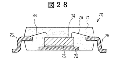
図28は従来のタブ露出型の半導体装置70の模式的断面図である。偏平四角形状の絶縁性樹脂からなる封止部71の下面中央にはタブ72の下面が露出している。このタブ72の上面には接合材73によって半導体チップ74が固定されている。封止部71の周面、即ち各辺の内外にはリード75が延在している。リード75はガルウィング型になっている。これらリード75の内端と半導体チップ74の電極(図示せず)は導電性のワイヤ76で電気的に接続されている。このような構造によれば、半導体チップ74で発生した熱をタブ72を介して外部に放散することができる。
【0009】
一方、地球環境悪化を抑制するために、半導体装置の実装に用いる接合材としては、鉛の含有量が少ない半田や、鉛を含まない半田(鉛フリー半田と呼称)が使用されている。この鉛フリー半田は、種々あるが、Sn−Ag−CuにZnやBiを添加した鉛フリー半田(融点240℃)が使用される。このような高融点半田の場合、半導体装置を半田を一時的に溶融(リフロー)して実装する場合、実装環境温度は240〜260℃と高くなる。
【0010】
本発明者においては、高温高湿の雰囲気下で寿命試験を行ったところ、薄いタブは剛性が低いため、反り等の変形が起き、半導体チップからタブが剥離する現象が発生するおそれがあることが判明した。このようなタブの剥離、即ち半導体チップとタブとの間に隙間が発生すると、この部分に水分が溜まり、半導体装置を実装基板にリフローにて実装する際、水分が膨張して水蒸気爆発を起こし実装不良が発生してしまう。
【0011】
本発明の目的は、放熱性が良好で実装の信頼性が高いタブ露出型半導体装置を提供することにある。
本発明の他の目的は、放熱性の良好なタブ露出型半導体装置を実装した実装の信頼性が高い電子装置及びその製造方法を提供することにある。
本発明の前記ならびにそのほかの目的と新規な特徴は、本明細書の記述および添付図面からあきらかになるであろう。
【0012】
【課題を解決するための手段】
本願において開示される発明のうち代表的なものの概要を簡単に説明すれば、下記のとおりである。
【0013】
(1)本発明の半導体装置は、封止部と、封止部の下面に下面が露出する厚さ0.125mm程度のタブと、封止部の内外に亘って延在し外端が外部電極端子となる複数のリードと、タブの上面にAgペースト材からなる接着材を介して固定される半導体チップと、半導体チップの電極とリードの内端部分を接続する導電性のワイヤとを有し、タブには封止部の内側に向かって屈曲して突出する凸部が設けられ、かつタブの下面全域が実装用の半田付け接合面となり、タブの面積は半導体チップの面積よりも大きくなり、凸部として半導体チップを固定するチップ搭載凸部と、封止部内に食い込む食い込み凸部とを有し、半導体チップはチップ搭載凸部の上面に固定されている。食い込み凸部はタブの縁に櫛歯状に設けられている。
【0014】
(2)本発明の電子装置は、実装基板と、この実装基板の上面に半田を介して実装される電子装置とからなっている。半導体装置は、封止部と、封止部の下面に下面が露出する厚さ0.125mm程度のタブと、封止部の内外に亘って延在し外端が外部電極端子となる複数のリードと、タブの上面にAgペースト材からなる接着材を介して固定される半導体チップと、半導体チップの電極とリードの内端部分を接続する導電性のワイヤとを有し、タブには封止部の内側に向かって突出する凸部が設けられ、かつタブの下面全域が実装用の半田付け接合面となり、タブの面積は半導体チップの面積よりも大きくなり、凸部として半導体チップを固定するチップ搭載凸部と、封止部内に食い込む食い込み凸部とを有し、半導体チップはチップ搭載凸部の上面に固定されている。食い込み凸部はタブの縁に櫛歯状に設けられている。半導体装置のタブ及び外部電極端子は実装基板に鉛フリー半田(例えば、Sn・Ag・CuにZnやBiを含む半田)を介して接合されている。
【0015】
このような電子装置は以下の方法で製造される。即ち、実装基板に接合材を介して半導体装置を実装する電子装置の製造方法であって、
前記半導体装置は、封止部と、前記封止部の下面に下面が露出する厚さ0.125mm程度のタブと、前記封止部の内外に亘って延在し外端が外部電極端子となる複数のリードと、前記タブの上面に接着材(Agペースト材)を介して固定される半導体チップと、前記半導体チップの電極と前記リードを接続する導電性のワイヤとを有し、前記タブには前記封止部の内側に突出する凸部(チップ搭載凸部及び食い込み凸部)が設けられ、前記タブの下面全域が実装用の半田付け接合面となることを特徴とし、
前記接合材による実装においては240℃以上の高温リフローによって、前記実装基板に前記タブ及び前記リードを鉛フリー半田を介して接合する。
【0016】
【発明の実施の形態】
以下、図面を参照して本発明の実施の形態を詳細に説明する。なお、発明の実施の形態を説明するための全図において、同一機能を有するものは同一符号を付け、その繰り返しの説明は省略する。
【0017】
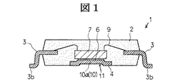
(実施形態1)
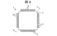
図1乃至図12は本発明の一実施形態(実施形態1)である半導体装置の製造方法に係わる図である。図1乃至図6は本実施形態1の半導体装置1の構造に係わる図である。図2乃至図4は外観を示す図であり、図1,図5及び図6は内部構造を示す断面図や一部を切り欠いた図である。
【0018】
本実施形態1の半導体装置1は、外観的には図2乃至図4に示すように、偏平四角形状の封止部2と、この封止部2の内外に亘って延在する複数のリード3とからなっている。リード3は、四角形の各辺から所定ピッチで突出する配列構成になっている。また、リード3はガルウィング型となり、半導体装置1が面実装できるようになっている。
【0019】
また、図1及び図4に示すように、封止部2の下面には、タブ(チップ搭載部)4が露出する構造になっている。四角形状のタブ4はその各角部がタブ吊りリード5で支持され、かつこのタブ吊りリード5は、図5に示すように途中で一段高く折り曲げられている。タブ吊りリード5の外端は、タブ4の端に沿って切断されている。四角形状のタブ4の一つの隅は切り欠くように斜めに切断されるように傾斜している。この傾斜面は、半導体装置1の方向性を認識するためのものである。
【0020】
タブ4の下面及びリード3の先端の実装部3bの下面は、略同一平面に位置している。これは、半導体装置1を実装基板に実装する際、リード3の実装部3bを接合材で実装基板の配線(接続のためのランド)に接合する際、実装基板に設けた熱放散パッドに接合材で接合するためである。従って、接合材による実装が確実に行えるならば、リード3の実装部3bの下面とタブ4の下面が必ずしも同一平面になくともよい。
【0021】
タブ4の上面には接着材6によって半導体チップ7が固定されている。そして、図6に示すように、半導体チップ7の電極8と各リード3の内端部分は導電性のワイヤ9で電気的に接続されている。接着材6としてはAgペースト材が使用されている。
【0022】
一方、これが本発明の特徴の一つであるが、タブ4は平坦な一枚板からなるものでなく、封止部2の内部に向かって突出する凸部10を有している。この凸部10は封止部2の中央に設けられ、半導体チップ7を搭載するチップ搭載凸部10aになっている。凸部10は、プレス金型による成形によって屈曲させて形成してある。従って、タブ4の下面には凸部10に対応しかつ凸部10よりも僅かに小さい凹部11が形成されることになる。例えば、凸部10の突出高さは70μm程度である。
【0023】
本発明では、凸部には、チップ搭載凸部の他に封止部に食い込んでタブが封止部から剥離しないような役割を果たす食い込み凸部が設けられる。この食い込み凸部を用いる例については後述する。
【0024】
タブ4は半導体チップ7よりも大きくなっている。これは半導体チップ7で発生した熱を速やかに外部に広く放熱するためであり、タブ4はヒートスプレッダ(放熱板)の役割を果たす。
【0025】
本実施形態1では、チップ搭載凸部10aは半導体チップ7よりも小さく形成され、半導体チップ7よりも面積が小さい部分で接着材6を介して半導体チップ7がタブ4に接着されている。これにより、半導体チップ7の裏面の一部も封止部2を形成する樹脂に接着されることになり、半導体チップ7と樹脂との接着面積の増大が図れ、耐湿性の向上を図ることができる。
【0026】
タブ4及びリード3は一枚の同じ厚さのリードフレームから形成される。リードフレームは、例えば、タブを介する熱放散を良好とするために、熱伝導性が良好な銅合金板等で形成される。また、タブの厚さ方向の熱抵抗を小さくするために、0.125mm程度と薄くなっている。半導体チップ7は、半導体基板に1乃至複数のトランジスタ等の能動素子を形成したものである。また、半導体基板は基準電位(グランド電位)となるように構成してもよい。この場合、導電性の接着材で半導体チップをタブに固定することによって、タブはグランド電位になる。
【0027】
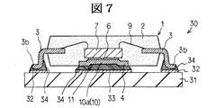
図7は本実施形態1の半導体装置1の実装構造、即ち電子装置30の一部を示す模式的断面図である。電子装置30は、実装基板31と、この実装基板31に実装された本実施形態1による半導体装置1等を実装した構造になっている。
【0028】
実装基板31の上面には所定の配線等が形成されているが、本実施形態1では半導体装置1のリード3の実装部3bに対応するランド32と、タブ4に対応する熱放散パッド33を模式的に示す。ランド32及び熱放散パッド33には、半導体装置1のリード3の実装部3b及びタブ4が接合材34によって電気的に接合されている。
【0029】
複数のランド32及び熱放散パッド33は、実装基板31の製造時に同時に形成され、同一の導体層をパターン化することによって形成される。また、ランド32及び熱放散パッド33の表面は図示しないメッキ膜が形成され、接合材34の濡れ性が良好になるようになっている。
【0030】
本実施形態1の電子装置の製造方法においては、即ち実装基板31に半導体装置1を実装する際、接合材34として鉛フリー半田を用いる。鉛フリー半田としては、例えば、融点が240℃程度となる、Sn−Ag−CuにZnやBiを添加した接合材が用いられる。また、実装の雰囲気としては、鉛フリー半田が酸化しない窒素雰囲気等で行われる。
【0031】
このような方法によれば、タブ4の反り等の変形が起き難くなり、半導体チップ7からタブ4が剥離する現象の発生を防止することができる。即ち、Agペースト材とタブ4との剥離が起き難くなる。
【0032】
また、本発明者は、240℃程度の温度下において、平坦な一枚板からなるタブ4の反り変形についてタブ4の厚さを変えて調べてみたところ、タブ4の厚さが0.25mm程度と薄くなると反り等の変形が発生することが分かった。しかし、本実施形態1のようにタブ4にチップ搭載凸部10aを設けることによってタブ4に反り等が発生せず、タブ4と接着材6(Agペースト材)との間に隙間が発生しないことも検証している。
【0033】
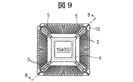
つぎに、図8乃至図12を参照しながら本実施形態1の半導体装置1の製造について説明する。半導体装置1の製造には、図8に示すように、製品形成部が複数設けられた銅合金板からなる厚さ0.125mm程度のリードフレーム15が用意される。
【0034】
製品形成部は単一の半導体装置1を形成する部分であり、図8には、縦横二つ合計4個が示されている。製品形成部fはエッチングや精密プレスによって所定のリードパターンを形成することによって形成され、かつプレスによって凸部10(チップ搭載凸部10a)等が設けられている。製品形成部fは、四角形枠に沿って延在するダム16と、前記四角形の中心に設けられるタブ4と、前記ダム16の各角部から四角形の対角線方向に延在し前記タブ4をタブ4の角部で支持するタブ吊りリード5と、ダム16の4辺の内外に亘って延在する複数のリード3とからなっている。また、タブ吊りリード5,ダム16及びリード3の外端はそれぞれフレーム枠17に支持されている。
【0035】
リード3はダム16の内外に亘って延在し、ダム16は四角形枠に沿って延在しと説明したが、リード3とダム16は交差し、ダム16は厳密にはリード3とリード3との間の部分またはリード3とフレーム枠17との部分であり、ダム16の内側から外側に直線的にリード3が延在することになる。
【0036】
図9及び図11はダムより内側のリードパターン、即ち製品形成部fのインナーリード部分のパターンを示すものである。図10は図9のB−B線に沿う断面図である。図10には、タブ吊りリード5が途中で下方に一段折り曲げられてタブ4を支持している状態、及びタブ4の中央が上面側に一段突出されてチップ搭載凸部10a(凸部10)が設けられている状態を示す。プレスによる成形のためチップ搭載凸部10aの反対面には凹部11が発生することになる。チップ搭載凸部10aの突出高さは、特に限定はされないが、70μm程度であり、従って、凹部11の窪み深さも70μm程度である。リードフレーム15は、図示しないが、チップ搭載部やリード3の実装部となる部分等に、必要に応じてメッキ膜が形成されている。
【0037】
このようなリードフレーム15を用意した後、図11に示すように、タブ4のチップ搭載凸部10a上(図1参照)に接合材としてAgペースト材を用いて半導体チップ7を固定(搭載)する。
【0038】
つぎに、図11に示すように、半導体チップ7の電極8とリード3の内端部分を導電性のワイヤ9で電気的に接続する。
【0039】
つぎに、図12に示すように、ダム16の内側の封止領域に、例えば、トランスファモールディング装置によって絶縁性樹脂からなる封止部2を形成する。
【0040】
つぎに、リード3とリード3の間のダム16、及びリード3とフレーム枠17との間のダム16を切断除去するとともに、リード3をフレーム枠17から切断して分離し、かつタブ吊りリード5を封止部2のつけ根で切断する。また、封止部2から突出するリード3を成形してリード3をガルウィング型とすることによって、図1乃至図3に示す半導体装置1を複数製造することができる。
【0041】
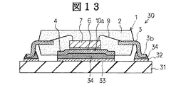
図13は本実施形態1の第1の変形例である半導体装置の実装状態(電子装置)の模式的断面図である。
【0042】
第1の変形例である半導体装置1は、実施形態1の半導体装置1において、タブ4のチップ搭載凸部10aの大きさを半導体チップ7よりも大きくし、半導体チップ7の下面全域がチップ搭載凸部10aの上面に接着材6を介して固定できるようにした例である。
【0043】
このような構成にすることによって、半導体チップ7とタブ4との接着面積が増大し、半導体チップ7からタブ4への熱の伝達量が増大する。従って、半導体装置1を電子装置30に実装した場合、半導体チップ7で発生した熱は、接着材6,タブ4,タブ4の下面全域に設けられた接合材34を通って実装基板31の熱放散パッド33に効率的にて伝達され、効率的な熱放散が可能になるため、電子装置30の耐熱信頼性が向上する。
【0044】
また、上記第1の変形例によれば、タブ4のチップ搭載凸部10aの大きさが上記半導体チップ7より大きいので、例えば、バーンイン試験時や半田実装時の熱履歴による応力によって、上記半導体チップ7にクラックが発生したり、上記半導体チップ7とチップ搭載凸部10a間に剥離が生じたりすることを抑制することが可能である。つまり、上記タブ4のチップ搭載凸部10aをチップと同等あるいは、大きくすることによって、上記半導体チップ7の応力に対する変曲点を実質的に無くすことができるので、チップ近傍での応力集中を抑制し、信頼性の高い半導体装置を提供できる。
【0045】
図14は本実施形態1の第2の変形例である半導体装置の実装状態の模式的断面図である。第2の変形例である半導体装置1は、実施形態1の半導体装置1において、チップ搭載凸部10aを複数とした例である。例えば、図14の場合はチップ搭載凸部10aを2列2行の状態で4個形成したものである。このように複数のチップ搭載凸部10aで1個の半導体チップ7を支持するようにしてもよい。チップ搭載凸部10aとチップ搭載凸部10aとの間には窪み10cが発生する。なお、半導体チップ7の大きさに近似した大きさのチップ搭載凸部10a(例えば、実施形態1の半導体装置)に、1乃至複数の窪み10cを設ける構成でもよい。
【0046】
図15は本実施形態1の第3の変形例である半導体装置の実装状態の模式的断面図である。第3の変形例である半導体装置1は、実施形態1の半導体装置1において、タブ4の大きさを半導体チップ7に対してさらに大きくしたものであり、熱放散性能をさらに高める構成である。即ち、本例におけるタブ4は、タブ4の端が半導体チップ7の端とリード3の内端との中間位置sよりも外側に位置するように大きくなっている。
本実施形態1によれば以下の効果を有する。
【0047】
(1)半導体チップ7を搭載するタブ4は、0.125mm程度と薄くなり、熱抵抗が小さくなり、熱放散性能が良好な半導体装置1になる。また、電子装置30は実装基板31と、この実装基板31上に接合材34(鉛フリー半田等)を介して接合された前記半導体装置1となるが、半導体装置1において、前述のようにタブ4は、0.125mm程度と薄くなり、熱抵抗が小さくなる結果、耐熱信頼性が良好な電子装置になる。
【0048】
(2)上記(1)のようにタブ4は薄くなっているが、タブ4には選択的に屈曲して形成されるチップ搭載凸部10a(凸部10)が設けられていることから、平坦な一枚板からなるタブ構造に比較して曲げ剛性及び強度が大きく(高く)なる。この結果、半導体装置1を実装基板31に接合材34(鉛フリー半田)を使用して接合する際の熱に起因するタブ4の反り等の変形を防止でき、半導体チップ7をタブ4に接着する接着材の劣化や剥がれを抑止できることになり、実装の信頼性が高い半導体装置1を提供することができる。また、この半導体装置1を実装した電子装置30は耐熱信頼性の高いものとなる。
【0049】
(3)上記(2)により、タブ4の曲げ剛性及び強度が大きくなることから、240℃程度と半田付け温度が高い高温リフローでの半導体装置1の実装が可能になる。この結果、半田付け温度が240℃程度となる鉛フリー半田による実装も可能になり、信頼性の高い電子装置30を提供することができる。
【0050】
(4)タブ4は半導体チップ7よりも大きくなっていることから、半導体チップ7で発生した熱を速やかに外部に広く放熱することができる。
【0051】
(5)チップ搭載凸部10aは半導体チップ7よりも小さく形成されていることから、封止部2を形成する樹脂が半導体チップ7の下面側にも接着されるため、半導体チップ7と樹脂との接着面積が増大し、耐湿性の向上を図ることができる。
【0052】
(6)第1の変形例のように、タブ4のチップ搭載凸部10aの面積を半導体チップ7の面積よりも大きくし、かつ半導体チップ7の下面全域をチップ搭載凸部10aの上面に接着材6を介して固定することによって放熱面積の増大が図れる。この結果、放熱性能が良好な半導体装置1及び耐熱信頼性が高い電子装置30を提供することができる。
【0053】
(7)第2の変形例のように、タブ4の端が半導体チップ7の端とリード3の内端との中間位置sよりも外側に位置するように、さらにタブ4を大きくすることによって放熱面積の増大が図れる。この結果、放熱性能が良好な半導体装置1及び耐熱信頼性が高い電子装置30を提供することができる。
【0054】
(実施形態2)
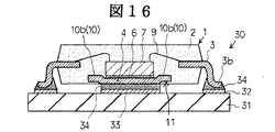
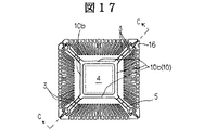
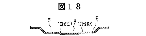
図16乃至図18は本発明の他の実施形態(実施形態2)である半導体装置に係わる図である。図16は半導体装置の実装状態を示す模式的断面図、図17は半導体装置の製造において用いるリードフレームのインナーリードパターンを示す平面図、図18は図17のC−C線に沿う拡大断面図である。
【0055】
本実施形態2の半導体装置1は、実施形態1の半導体装置1において、タブ4の断面形状が異なるだけである。即ち、本実施形態2の場合は、タブ4に設ける凸部10はタブ4の周辺に沿って設けられている。この凸部10は、タブ4の下面よりも下面が浮き上がる凸部10であることから、封止部2の内部に食い込む食い込み凸部10bになる。そして、タブ4の平坦面上に半導体チップ7を接着材6によって固定した構造になっている。食い込み凸部10bは上下面が封止部2内に位置する。
【0056】
このように、タブ4には封止部2内に食い込む食い込み凸部10bを有することから、タブ4は封止部2から抜け難くなり、半導体チップ7のタブ4からの剥離を防止することができる。
【0057】
図17は半導体装置1の製造に用いるリードフレーム15のインナーリードパターンを示す図であり、図18は図17のC−C線に沿う拡大断面図である。図16及び図18からも分かるように、タブ4の全周縁がプレス成形によって一段高く突出して食い込み凸部10bが形成されている。
【0058】
また、本実施形態2では、半導体チップ7の下面全域が接着材6によって平坦なタブ4の上面に固定され、放熱性能を向上させている。
【0059】
本実施形態2においても、実施形態1の場合と同様に放熱性が良好で実装の信頼性が高いタブ露出型半導体装置の提供、放熱性の良好なタブ露出型半導体装置を実装した実装の信頼性が高い電子装置の提供が可能になる。
【0060】
図19は本実施形態2の変形例である半導体装置の実装状態の模式的断面図である。変形例である半導体装置1は、実施形態2の半導体装置1において、半導体チップ7の下面の周縁部分はタブ4に固定されず、その隙間には封止部2を形成する樹脂が入り込む構造となっている。この結果、半導体チップ7と樹脂との接着面積が増大し、半導体装置1の耐湿性を向上させることができる。
【0061】
(実施形態3)
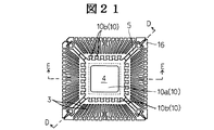
図20乃至図23は本発明の他の実施形態(実施形態3)である半導体装置に係わる図である。図20は半導体装置の実装状態を示す模式的断面図、図21は半導体装置の製造において用いるリードフレームのインナーリードパターンを示す平面図、図22は図21のD−D線に沿う拡大断面図、図23は図21のE−E線に沿う拡大断面図である。
【0062】
本実施形態3の半導体装置1は、実施形態1の半導体装置1において、タブ4の周縁の食い込み凸部10bを、図21のインナーリードパターンの図で示すように櫛歯状に形成したものである。この櫛歯状の食い込み凸部10bは、図20に示すように、傾斜するように折り曲げられて形成されている。本実施形態3は、タブ4の中央側にチップ搭載凸部10a(凸部10)が設けられ、タブ4の周縁に食い込み凸部10b(凸部10)が設けられる例である。
【0063】
また、櫛歯状の一つ一つの食い込み凸部10bは、つけ根部分よりも先端の幅が広くなる構造になり、食い込み凸部10bが封止部2からさらに抜け難い構造になっている。この結果、タブ4の封止部2からの脱落が防止できる。この幅の違う構造は、食い込み凸部10bを傾斜させたることによってさらに抜け抑止効果が増大する。即ち、実施形態2の場合のように、タブ4の平坦部分と、この平坦部分に平行に延在する食い込み凸部10bとの関係に比較し、櫛歯状の一つ一つの食い込み凸部10bが先端に向かうほど幅が広くなる構造では、抜け方向に対して幅広部分が引っ掛かるようになることから抜け防止に効果がある。
【0064】
図23は食い込み凸部10bが設けられないタブ4部分の断面図であり、図22はタブ吊りリード5の延在方向に沿う断面図である。図22には食い込み凸部10bが現れている。本実施形態3では、櫛歯状の一つ一つの食い込み凸部10bが先端に向かうに従って徐々に幅が広くなる構造としたが、段付き構造やその組み合わせの構造でも同様の効果を得ることができる。
【0065】
本実施形態3においても、実施形態1の場合と同様に放熱性が良好で実装の信頼性が高いタブ露出型半導体装置の提供、放熱性の良好なタブ露出型半導体装置を実装した実装の信頼性が高い電子装置の提供が可能になる。
【0066】
(実施形態4)
図24は本発明の他の実施形態(実施形態4)である半導体装置の実装状態の模式的断面図、即ち電子装置30の一部を示す図である。
【0067】
本実施形態4は実施形態1の半導体装置1において、リード3の実装部3bを封止部2の下面に露出させるノンリード型半導体装置構造としたものである。即ち、封止部(パッケージ)2の側方に意図的に外部電極端子を突出させることなく封止部2の下面である実装面側にリード3の実装部3bを露出させるものである。封止部2の下面にリード3の実装部3bの下面を露出させるために、封止部2は片面モールディングによって形成されるため、断面形状は実施形態1のものとはやや異なる。他の部分は実施形態1の半導体装置1と同じである。露出するリード(外部電極端子)の配置から、本実施形態4の半導体装置1はQFN(Quad Flat Non−Leaded Package)構造である。本発明は、同様に封止部2の下面の両側に外部電極端子を配列するSON(Small Outline Non−Leaded Package)にも適用できる。
【0068】
本実施形態4においても、実施形態1の場合と同様に放熱性が良好で実装の信頼性が高いタブ露出型半導体装置の提供、放熱性の良好なタブ露出型半導体装置を実装した実装の信頼性が高い電子装置の提供が可能になる。
【0069】
(実施形態5)
図25は本発明の他の実施形態(実施形態5)である半導体装置の実装状態の模式的断面図である。本実施形態5の半導体装置1は、実施形態1の第1の変形例の構造に櫛歯状の食い込み凸部10bを設けたリード3がガルウィング型になる構成である。即ち、本実施形態5の半導体装置1は、実施形態1の半導体装置1において、タブ4のチップ搭載凸部10aの大きさを半導体チップ7よりも大きくし、半導体チップ7の下面全域がチップ搭載凸部10aの上面に接着材6を介して固定できるようにした例であり、かつ実施形態3のようにタブ4の周縁に櫛歯状に食い込み凸部10bを設けたものである。
【0070】
本実施形態5においても、実施形態1の場合と同様に放熱性が良好で実装の信頼性が高いタブ露出型半導体装置の提供、放熱性の良好なタブ露出型半導体装置を実装した実装の信頼性が高い電子装置の提供が可能になる。
【0071】
(実施形態6)
図26は本発明の他の実施形態(実施形態6)である半導体装置の実装状態の模式的断面図である。本実施形態6の半導体装置1は、実施形態5の半導体装置1をノンリード型半導体装置にしたものである。
【0072】
本実施形態6においても、実施形態1の場合と同様に放熱性が良好で実装の信頼性が高いタブ露出型半導体装置の提供、放熱性の良好なタブ露出型半導体装置を実装した実装の信頼性が高い電子装置の提供が可能になる。
【0073】
(実施形態7)
図27は本発明の他の実施形態(実施形態7)である半導体装置の実装状態の模式的断面図である。本実施形態7の半導体装置1は実施形態2の半導体装置1(図16)において、平坦な一枚板からなるタブ4の周縁に、櫛歯状の食い込み凸部10bを設けた例である。櫛歯状の一つ一つの食い込み凸部10bは、実施形態3の半導体装置1(図20)と同様に傾斜した構造になり、かつ一つ一つの食い込み凸部10bは先端に向かって徐々に幅が広い構造になっている。
【0074】
本実施形態7においても、実施形態1の場合と同様に放熱性が良好で実装の信頼性が高いタブ露出型半導体装置の提供、放熱性の良好なタブ露出型半導体装置を実装した実装の信頼性が高い電子装置の提供が可能になる。
以上本発明者によってなされた発明を実施形態に基づき具体的に説明したが、本発明は上記実施形態に限定されるものではなく、その要旨を逸脱しない範囲で種々変更可能であることはいうまでもない。
【0075】
【発明の効果】
本願において開示される発明のうち代表的なものによって得られる効果を簡単に説明すれば、下記のとおりである。
【0076】
(1)放熱性が良好で実装の信頼性が高いタブ露出型半導体装置を提供することができる。
【0077】
(2)放熱性の良好なタブ露出型半導体装置を実装した実装の信頼性が高い電子装置を提供することができる。
【0078】
(3)放熱性の良好なタブ露出型半導体装置を実装した実装の信頼性が高い電子装置の製造方法を提供することができる。
【図面の簡単な説明】
【図1】本発明の一実施形態(実施形態1)である半導体装置の模式的断面図である。
【図2】本実施形態1の半導体装置の平面図である。
【図3】本実施形態1の半導体装置の側面図である。
【図4】本実施形態1の半導体装置の底面図である。
【図5】図2のA−A線に沿う模式的断面図である。
【図6】本実施形態1の半導体装置において封止部の一部を取り除いた状態を示す模式的平面図である。
【図7】本実施形態1の半導体装置の実装状態を示す模式的断面図である。
【図8】本実施形態1の半導体装置の製造方法で使用するリードフレームの平面図である。
【図9】前記リードフレームの製品形成部のインナーリードパターンを示す平面図である。
【図10】図9のB−B線に沿う拡大断面図である。
【図11】前記リードフレームに半導体チップを固定し、ワイヤボンディングが終了したインナーリードを含む一部の模式的平面図である。
【図12】本実施形態1の半導体装置の製造方法において、封止部を形成した状態を示す製品形成部分の平面図である。
【図13】本実施形態1の第1の変形例である半導体装置の実装状態の模式的断面図である。
【図14】本実施形態1の第2の変形例である半導体装置の実装状態の模式的断面図である。
【図15】本実施形態1の第3の変形例である半導体装置の実装状態の模式的断面図である。
【図16】本発明の他の実施形態(実施形態2)である半導体装置の実装状態の模式的断面図である。
【図17】本実施形態2の半導体装置の製造において用いるリードフレームのインナーリードパターンを示す平面図である。
【図18】図17のC−C線に沿う拡大断面図である。
【図19】本実施形態2の変形例である半導体装置の実装状態の模式的断面図である。
【図20】本発明の他の実施形態(実施形態3)である半導体装置の実装状態の模式的断面図である。
【図21】本実施形態3の半導体装置の製造において用いるリードフレームのインナーリードパターンを示す平面図である。
【図22】図21のD−D線に沿う拡大断面図である。
【図23】図21のE−E線に沿う拡大断面図である。
【図24】本発明の他の実施形態(実施形態4)である半導体装置の実装状態の模式的断面図である。
【図25】本発明の他の実施形態(実施形態5)である半導体装置の実装状態の模式的断面図である。
【図26】本発明の他の実施形態(実施形態6)である半導体装置の実装状態の模式的断面図である。
【図27】本発明の他の実施形態(実施形態7)である半導体装置の実装状態の模式的断面図である。
【図28】従来の半導体装置の断面図である。
【符号の説明】
1…半導体装置、2…封止部(パッケージ)、3…リード、3b…実装部、4…タブ(チップ搭載部)、5…タブ吊りリード、6…接着材、7…半導体チップ、8…電極、9…ワイヤ、10…凸部、10a…チップ搭載凸部、10b…食い込み凸部、10c…窪み、11…凹部、15…リードフレーム、16…ダム、17…フレーム枠、30…電子装置、31…実装基板、32…ランド、33…熱放散パッド、34…接合材、70…半導体装置、71…封止部、72…タブ、73…接合材、74…半導体チップ、75…リード、76…ワイヤ。[0001]
TECHNICAL FIELD OF THE INVENTION
The present invention relates to a semiconductor device and a technology for manufacturing an electronic device incorporating the semiconductor device, and more particularly to a resin-sealed semiconductor that exposes a lower surface of a tab on which a semiconductor chip is mounted on a lower surface of a sealing portion formed of an insulating resin. It relates to technology that is effective when applied to equipment.
[0002]
[Prior art]
2. Description of the Related Art A resin-sealed semiconductor device is known as a sealed semiconductor device which is highly mass-producible and enables cost reduction. Also, in order to quickly dissipate the heat generated by the semiconductor chip incorporated in the sealing portion (package) to the outside of the sealing portion, the back surface (lower surface) of the support plate (tab) to which the semiconductor chip is fixed is sealed. A structure that exposes the back surface (lower surface) of a portion is known (for example, see Patent Document 1).
[0003]
This
[0004]
[Patent Document 1]
JP 2001-77136 A (
[0005]
[Problems to be solved by the invention]
2. Description of the Related Art In a resin-sealed semiconductor device, a lead frame in which a metal plate has a predetermined lead pattern is used. A lead frame is also used in a resin-sealed semiconductor device having a structure in which a lower surface of a tab is exposed on a lower surface of a sealing portion (hereinafter, also simply referred to as a tab-exposed type). A lead frame generally has a structure in which a plurality of products can be manufactured from one lead frame. A tab for fixing the semiconductor chip is included in a product forming part where a product is formed.
[0006]
The power consumption of a semiconductor chip (semiconductor element) incorporated in a sealing portion (package) of a semiconductor device also tends to increase temporarily due to a demand for multifunctional and high-output semiconductor devices. In such high power consumption products, it is necessary to dissipate the heat generated in the semiconductor element to the outside of the sealing portion more quickly, and the thickness of the tab on which the semiconductor chip is mounted tends to be smaller due to a reduction in thermal resistance. .
[0007]
For example, in the case of a drive semiconductor device of a hard disk drive (HDD) device, the number of external electrode terminals (the number of pins) is 64, and the package structure is a QFP [Quad] in which leads protrude from four sides of a rectangular sealing portion. [Flat Non-Leaded Package] type. This semiconductor device is connected to a printed wiring board (PWB), which is a mounting substrate, by soldering, and radiates heat generated in the semiconductor chip to the mounting substrate via tabs and solder. As a result, in order to improve the heat dissipation, for example, the tab is required to be as thin as about 0.25 to 0.125 mm.
[0008]
FIG. 28 is a schematic cross-sectional view of a conventional tab-exposed
[0009]
On the other hand, in order to suppress the deterioration of the global environment, solder having a low lead content or solder containing no lead (referred to as lead-free solder) is used as a bonding material for mounting a semiconductor device. Although there are various types of lead-free solder, lead-free solder (melting point 240 ° C.) obtained by adding Zn or Bi to Sn—Ag—Cu is used. In the case of such a high melting point solder, when the semiconductor device is temporarily melted (reflowed) and mounted, the mounting environment temperature is as high as 240 to 260 ° C.
[0010]
In the present inventor, when a life test was performed in a high-temperature, high-humidity atmosphere, the thin tab had low rigidity, so deformation such as warpage might occur, and a phenomenon that the tab was peeled from the semiconductor chip might occur. There was found. If such a separation of the tab, that is, a gap is generated between the semiconductor chip and the tab, moisture accumulates in this portion, and when the semiconductor device is mounted on the mounting board by reflow, the moisture expands and causes a steam explosion. Mounting defects will occur.
[0011]
An object of the present invention is to provide a tab-exposed type semiconductor device having good heat dissipation and high mounting reliability.
Another object of the present invention is to provide an electronic device in which a tab-exposed type semiconductor device having good heat dissipation is mounted and has high mounting reliability, and a method of manufacturing the same.
The above and other objects and novel features of the present invention will become apparent from the description of the present specification and the accompanying drawings.
[0012]
[Means for Solving the Problems]
The outline of a typical invention among the inventions disclosed in the present application will be briefly described as follows.
[0013]
(1) The semiconductor device of the present invention includes a sealing portion, a tab having a thickness of about 0.125 mm whose lower surface is exposed at the lower surface of the sealing portion, and an outer end extending outside and inside the sealing portion. The semiconductor device includes a plurality of leads serving as electrode terminals, a semiconductor chip fixed to an upper surface of the tab via an adhesive made of an Ag paste material, and a conductive wire connecting an electrode of the semiconductor chip and an inner end of the lead. Then, the tab is provided with a convex portion that bends and projects toward the inside of the sealing portion, and the entire lower surface of the tab becomes a soldering joint surface for mounting, and the area of the tab is larger than the area of the semiconductor chip. The semiconductor chip is fixed to the upper surface of the chip mounting protrusion, and has a chip mounting protrusion fixing the semiconductor chip as the protrusion, and a biting protrusion that cuts into the sealing portion. The biting projection is provided in a comb-like shape on the edge of the tab.
[0014]
(2) The electronic device of the present invention includes a mounting board and an electronic device mounted on the upper surface of the mounting board via solder. The semiconductor device has a sealing portion, a tab having a thickness of about 0.125 mm whose lower surface is exposed to the lower surface of the sealing portion, and a plurality of tabs extending over the inside and outside of the sealing portion and having outer ends serving as external electrode terminals. The semiconductor device includes a lead, a semiconductor chip fixed on the upper surface of the tab via an adhesive made of an Ag paste material, and a conductive wire for connecting an electrode of the semiconductor chip to an inner end portion of the lead. A convex portion protruding toward the inside of the stop is provided, and the entire lower surface of the tab becomes a soldering joint surface for mounting, the area of the tab becomes larger than the area of the semiconductor chip, and the semiconductor chip is fixed as a convex portion The semiconductor chip is fixed to the upper surface of the chip mounting protrusion, which has a chip mounting protrusion to be inserted and a biting protrusion that cuts into the sealing portion. The biting projection is provided in a comb-like shape on the edge of the tab. The tab and the external electrode terminal of the semiconductor device are joined to the mounting substrate via lead-free solder (for example, solder containing Zn, Bi, and Sn, Ag, and Cu).
[0015]
Such an electronic device is manufactured by the following method. That is, a method of manufacturing an electronic device in which a semiconductor device is mounted on a mounting board via a bonding material,
The semiconductor device has a sealing portion, a tab having a thickness of about 0.125 mm whose lower surface is exposed on the lower surface of the sealing portion, and an outer end extending over the inside and outside of the sealing portion and having an external electrode terminal. A plurality of leads, a semiconductor chip fixed to an upper surface of the tab via an adhesive (Ag paste material), and a conductive wire connecting an electrode of the semiconductor chip to the lead. Is provided with a convex portion (a chip mounting convex portion and a biting convex portion) protruding inside the sealing portion, and the entire lower surface of the tab serves as a soldering joint surface for mounting,
In mounting with the bonding material, the tab and the lead are bonded to the mounting board via a lead-free solder by high-temperature reflow of 240 ° C. or more.
[0016]
BEST MODE FOR CARRYING OUT THE INVENTION
Hereinafter, embodiments of the present invention will be described in detail with reference to the drawings. In all the drawings for describing the embodiments of the present invention, components having the same functions are denoted by the same reference numerals, and their repeated description will be omitted.
[0017]
(Embodiment 1)
1 to 12 are diagrams related to a method for manufacturing a semiconductor device according to an embodiment (Embodiment 1) of the present invention. 1 to 6 are diagrams related to the structure of the
[0018]
As shown in FIGS. 2 to 4, the
[0019]
Further, as shown in FIGS. 1 and 4, a tab (chip mounting portion) 4 is exposed on the lower surface of the sealing
[0020]
The lower surface of the
[0021]
A
[0022]
On the other hand, this is one of the features of the present invention, but the
[0023]
In the present invention, in addition to the chip mounting protrusion, the protrusion is provided with a biting protrusion serving to prevent the tab from being separated from the sealing portion by cutting into the sealing portion. An example in which this biting projection is used will be described later.
[0024]
The
[0025]
In the first embodiment, the
[0026]
The
[0027]
FIG. 7 is a schematic sectional view showing a mounting structure of the
[0028]
Although a predetermined wiring or the like is formed on the upper surface of the mounting
[0029]
The plurality of
[0030]
In the method for manufacturing an electronic device according to the first embodiment, that is, when the
[0031]
According to such a method, deformation such as warpage of the
[0032]
Further, the present inventor examined the warpage deformation of the
[0033]
Next, the manufacture of the
[0034]
The product forming part is a part that forms a
[0035]
Although it has been described that the
[0036]
9 and 11 show a lead pattern inside the dam, that is, a pattern of an inner lead portion of the product forming portion f. FIG. 10 is a sectional view taken along line BB of FIG. FIG. 10 shows a state in which the
[0037]
After preparing such a
[0038]
Next, as shown in FIG. 11, the electrodes 8 of the
[0039]
Next, as shown in FIG. 12, the sealing
[0040]
Next, the
[0041]
FIG. 13 is a schematic cross-sectional view of a mounted state (electronic device) of a semiconductor device according to a first modification of the first embodiment.
[0042]
The
[0043]
With such a configuration, the bonding area between the
[0044]
Further, according to the first modification, the size of the
[0045]
FIG. 14 is a schematic sectional view of a mounted state of a semiconductor device according to a second modification of the first embodiment. A
[0046]
FIG. 15 is a schematic cross-sectional view of a mounted state of a semiconductor device according to a third modification of the first embodiment. The
According to the first embodiment, the following effects can be obtained.
[0047]
(1) The
[0048]
(2) Although the
[0049]
(3) According to the above (2), the bending rigidity and strength of the
[0050]
(4) Since the
[0051]
(5) Since the
[0052]
(6) As in the first modification, the area of the
[0053]
(7) As in the second modification, the
[0054]
(Embodiment 2)
FIGS. 16 to 18 relate to a semiconductor device according to another embodiment (Embodiment 2) of the present invention. 16 is a schematic cross-sectional view showing a mounting state of the semiconductor device, FIG. 17 is a plan view showing an inner lead pattern of a lead frame used in manufacturing the semiconductor device, and FIG. 18 is an enlarged cross-sectional view taken along line CC of FIG. It is.
[0055]
The
[0056]
As described above, since the
[0057]
FIG. 17 is a diagram showing an inner lead pattern of the
[0058]
In the second embodiment, the entire lower surface of the
[0059]
Also in the second embodiment, as in the first embodiment, the provision of the tab-exposed semiconductor device having good heat dissipation and high mounting reliability, and the reliability of the mounting of the tab-exposed semiconductor device having good heat dissipation. An electronic device with high reliability can be provided.
[0060]
FIG. 19 is a schematic cross-sectional view of a mounted state of a semiconductor device according to a modification of the second embodiment. The
[0061]
(Embodiment 3)
20 to 23 are diagrams related to a semiconductor device according to another embodiment (Embodiment 3) of the present invention. 20 is a schematic cross-sectional view showing a mounting state of the semiconductor device, FIG. 21 is a plan view showing an inner lead pattern of a lead frame used in manufacturing the semiconductor device, and FIG. 22 is an enlarged cross-sectional view taken along line DD of FIG. FIG. 23 is an enlarged sectional view taken along line EE of FIG.
[0062]
The
[0063]
In addition, each of the comb-teeth-shaped biting
[0064]
FIG. 23 is a cross-sectional view of the portion of the
[0065]
Also in the third embodiment, as in the first embodiment, the provision of a tab-exposed type semiconductor device having good heat dissipation and high mounting reliability, and the reliability of mounting with the tab-exposed type semiconductor device having good heat dissipation. An electronic device with high reliability can be provided.
[0066]
(Embodiment 4)
FIG. 24 is a schematic sectional view of a mounted state of a semiconductor device according to another embodiment (Embodiment 4) of the present invention, that is, a diagram showing a part of the
[0067]
In the fourth embodiment, the
[0068]
Also in the fourth embodiment, as in the first embodiment, the provision of a tab-exposed semiconductor device having good heat dissipation and high mounting reliability, and the reliability of mounting a tab-exposed semiconductor device having good heat dissipation, are provided. An electronic device with high reliability can be provided.
[0069]
(Embodiment 5)
FIG. 25 is a schematic sectional view of a mounted state of a semiconductor device according to another embodiment (Embodiment 5) of the present invention. The
[0070]
Also in the fifth embodiment, as in the case of the first embodiment, the provision of a tab-exposed type semiconductor device having good heat dissipation and high mounting reliability, and the reliability of mounting the tab-exposed type semiconductor device having good heat dissipation. An electronic device with high reliability can be provided.
[0071]
(Embodiment 6)
FIG. 26 is a schematic sectional view of a mounted state of a semiconductor device according to another embodiment (Embodiment 6) of the present invention. The
[0072]
Also in the sixth embodiment, as in the first embodiment, the provision of a tab-exposed semiconductor device having good heat dissipation and high mounting reliability, and the reliability of the mounting of the tab-exposed semiconductor device having good heat dissipation. An electronic device with high reliability can be provided.
[0073]
(Embodiment 7)
FIG. 27 is a schematic sectional view of a mounted state of a semiconductor device according to another embodiment (Embodiment 7) of the present invention. The
[0074]
Also in the seventh embodiment, as in the first embodiment, the provision of the tab-exposed semiconductor device having good heat dissipation and high mounting reliability, and the reliability of the mounting of the tab-exposed semiconductor device having good heat dissipation. An electronic device with high reliability can be provided.
Although the invention made by the inventor has been specifically described based on the embodiment, the present invention is not limited to the above embodiment, and various changes can be made without departing from the gist of the invention. Nor.
[0075]
【The invention's effect】
The effects obtained by the typical inventions among the inventions disclosed in the present application will be briefly described as follows.
[0076]
(1) It is possible to provide a tab-exposed type semiconductor device having good heat dissipation and high mounting reliability.
[0077]
(2) It is possible to provide an electronic device having high reliability of mounting on which a tab-exposed semiconductor device having good heat dissipation is mounted.
[0078]
(3) It is possible to provide a method of manufacturing an electronic device in which a tab-exposed semiconductor device having good heat dissipation is mounted and mounting is highly reliable.
[Brief description of the drawings]
FIG. 1 is a schematic cross-sectional view of a semiconductor device according to an embodiment (Embodiment 1) of the present invention.
FIG. 2 is a plan view of the semiconductor device according to the first embodiment.
FIG. 3 is a side view of the semiconductor device according to the first embodiment.
FIG. 4 is a bottom view of the semiconductor device according to the first embodiment.
FIG. 5 is a schematic sectional view taken along line AA of FIG. 2;
FIG. 6 is a schematic plan view showing a state where a part of a sealing portion is removed in the semiconductor device of the first embodiment.
FIG. 7 is a schematic cross-sectional view showing a mounted state of the semiconductor device of the first embodiment.
FIG. 8 is a plan view of a lead frame used in the method of manufacturing a semiconductor device according to the first embodiment.
FIG. 9 is a plan view showing an inner lead pattern of a product forming portion of the lead frame.
FIG. 10 is an enlarged sectional view taken along the line BB of FIG. 9;
FIG. 11 is a schematic plan view of a part including an inner lead in which a semiconductor chip is fixed to the lead frame and wire bonding is completed.
FIG. 12 is a plan view of a product forming portion showing a state in which a sealing portion is formed in the method of manufacturing a semiconductor device according to the first embodiment.
FIG. 13 is a schematic cross-sectional view of a mounted state of a semiconductor device according to a first modification of the first embodiment.
FIG. 14 is a schematic cross-sectional view of a mounted state of a semiconductor device according to a second modification of the first embodiment.
FIG. 15 is a schematic cross-sectional view of a semiconductor device according to a third modification of the first embodiment in a mounted state.
FIG. 16 is a schematic cross-sectional view of a mounted state of a semiconductor device according to another embodiment (Embodiment 2) of the present invention.
FIG. 17 is a plan view showing an inner lead pattern of a lead frame used in manufacturing the semiconductor device of the second embodiment.
FIG. 18 is an enlarged sectional view taken along line CC of FIG. 17;
FIG. 19 is a schematic sectional view of a mounted state of a semiconductor device according to a modification of the second embodiment.
FIG. 20 is a schematic cross-sectional view of a mounted state of a semiconductor device according to another embodiment (Embodiment 3) of the present invention.
FIG. 21 is a plan view showing an inner lead pattern of a lead frame used in manufacturing the semiconductor device of the third embodiment.
FIG. 22 is an enlarged sectional view taken along line DD of FIG. 21.
FIG. 23 is an enlarged sectional view taken along line EE in FIG. 21;
FIG. 24 is a schematic cross-sectional view of a mounted state of a semiconductor device according to another embodiment (Embodiment 4) of the present invention.
FIG. 25 is a schematic sectional view of a mounted state of a semiconductor device according to another embodiment (Embodiment 5) of the present invention.
FIG. 26 is a schematic sectional view of a mounted state of a semiconductor device according to another embodiment (Embodiment 6) of the present invention.
FIG. 27 is a schematic sectional view of a mounted state of a semiconductor device according to another embodiment (Embodiment 7) of the present invention.
FIG. 28 is a sectional view of a conventional semiconductor device.
[Explanation of symbols]
DESCRIPTION OF
Claims (33)
前記封止部の下面に下面が露出するタブと、
前記封止部の内外に亘って延在し外端が外部電極端子となる複数のリードと、
前記タブの上面に接着材を介して固定される半導体チップと、
前記半導体チップの電極と前記リードを接続する導電性のワイヤとを有し、
前記タブには前記封止部の内側に突出する凸部が設けられ、
前記タブの下面全域が実装用の半田付け接合面となることを特徴とする半導体装置。A sealing portion,
A tab whose lower surface is exposed on the lower surface of the sealing portion,
A plurality of leads extending over the inside and outside of the sealing portion and having outer ends serving as external electrode terminals,
A semiconductor chip fixed to the upper surface of the tab via an adhesive,
Having a conductive wire connecting the electrode of the semiconductor chip and the lead,
The tab is provided with a convex portion protruding inside the sealing portion,
A semiconductor device, wherein the entire lower surface of the tab serves as a soldering joint surface for mounting.
前記半導体装置は、
封止部と、
前記封止部の下面に下面が露出するタブと、
前記封止部の内外に亘って延在する複数のリードと、
前記タブの上面に接着材を介して固定される半導体チップと、
前記半導体チップの電極と前記リードを接続する導電性のワイヤとを有し、
前記タブには前記封止部の内側に突出する凸部が設けられる構造となり、
前記タブの下面全域が半田によって前記実装基板に実装されていることを特徴とする電子装置。An electronic device comprising a mounting board and a semiconductor device mounted on a top surface of the mounting board via a bonding material,
The semiconductor device includes:
A sealing portion,
A tab whose lower surface is exposed on the lower surface of the sealing portion,
A plurality of leads extending over the inside and outside of the sealing portion,
A semiconductor chip fixed to the upper surface of the tab via an adhesive,
Having a conductive wire connecting the electrode of the semiconductor chip and the lead,
The tab has a structure in which a convex portion protruding inside the sealing portion is provided,
An electronic device, wherein the entire lower surface of the tab is mounted on the mounting board by soldering.
前記半導体装置は、封止部と、前記封止部の下面に下面が露出するタブと、前記封止部の内外に亘って延在し外端が外部電極端子となる複数のリードと、前記タブの上面に接着材を介して固定される半導体チップと、前記半導体チップの電極と前記リードを接続する導電性のワイヤとを有し、前記タブには前記封止部の内側に突出する凸部が設けられ、前記タブの下面全域が実装用の半田付け接合面となることを特徴とし、
前記接合材による実装においては240℃以上の高温リフローによって、前記実装基板に前記タブ及び前記リードを前記接合材を介して接合する電子装置の製造方法。A method of manufacturing an electronic device for mounting a semiconductor device on a mounting board via a bonding material,
The semiconductor device includes a sealing portion, a tab having a lower surface exposed at a lower surface of the sealing portion, a plurality of leads extending over the inside and outside of the sealing portion and having outer ends serving as external electrode terminals, A semiconductor chip fixed to an upper surface of the tab via an adhesive, and a conductive wire connecting the electrode of the semiconductor chip and the lead, wherein the tab has a protrusion protruding inside the sealing portion. Portion is provided, wherein the entire lower surface of the tab is a soldering joint surface for mounting,
A method for manufacturing an electronic device, comprising: bonding the tab and the lead to the mounting substrate via the bonding material by high-temperature reflow of 240 ° C. or more when mounting with the bonding material.
Priority Applications (1)
| Application Number | Priority Date | Filing Date | Title |
|---|---|---|---|
| JP2003018797A JP2004235217A (en) | 2003-01-28 | 2003-01-28 | Semiconductor device and method for manufacturing electronic device |
Applications Claiming Priority (1)
| Application Number | Priority Date | Filing Date | Title |
|---|---|---|---|
| JP2003018797A JP2004235217A (en) | 2003-01-28 | 2003-01-28 | Semiconductor device and method for manufacturing electronic device |
Publications (1)
| Publication Number | Publication Date |
|---|---|
| JP2004235217A true JP2004235217A (en) | 2004-08-19 |
Family
ID=32948836
Family Applications (1)
| Application Number | Title | Priority Date | Filing Date |
|---|---|---|---|
| JP2003018797A Pending JP2004235217A (en) | 2003-01-28 | 2003-01-28 | Semiconductor device and method for manufacturing electronic device |
Country Status (1)
| Country | Link |
|---|---|
| JP (1) | JP2004235217A (en) |
Cited By (6)
| Publication number | Priority date | Publication date | Assignee | Title |
|---|---|---|---|---|
| JP2007054972A (en) * | 2005-08-22 | 2007-03-08 | Apic Yamada Corp | Resin mold |
| JP2007194379A (en) * | 2006-01-19 | 2007-08-02 | Matsushita Electric Ind Co Ltd | Lead frame, semiconductor device, and method of manufacturing same |
| JP2008270661A (en) * | 2007-04-24 | 2008-11-06 | Mitsui High Tec Inc | Lead frame, lead frame manufacturing method, semiconductor device, and semiconductor device manufacturing method |
| JP2009076658A (en) * | 2007-09-20 | 2009-04-09 | Renesas Technology Corp | Semiconductor device and manufacturing method thereof |
| JP2013251489A (en) * | 2012-06-04 | 2013-12-12 | Denso Corp | Manufacturing method of mold package |
| US8912640B2 (en) | 2011-07-04 | 2014-12-16 | Renesas Electronics Corporation | Semiconductor device and method of manufacturing the same |
-
2003
- 2003-01-28 JP JP2003018797A patent/JP2004235217A/en active Pending
Cited By (7)
| Publication number | Priority date | Publication date | Assignee | Title |
|---|---|---|---|---|
| JP2007054972A (en) * | 2005-08-22 | 2007-03-08 | Apic Yamada Corp | Resin mold |
| JP2007194379A (en) * | 2006-01-19 | 2007-08-02 | Matsushita Electric Ind Co Ltd | Lead frame, semiconductor device, and method of manufacturing same |
| JP2008270661A (en) * | 2007-04-24 | 2008-11-06 | Mitsui High Tec Inc | Lead frame, lead frame manufacturing method, semiconductor device, and semiconductor device manufacturing method |
| JP2009076658A (en) * | 2007-09-20 | 2009-04-09 | Renesas Technology Corp | Semiconductor device and manufacturing method thereof |
| US8912640B2 (en) | 2011-07-04 | 2014-12-16 | Renesas Electronics Corporation | Semiconductor device and method of manufacturing the same |
| US9252088B2 (en) | 2011-07-04 | 2016-02-02 | Renesas Electronics Corporation | Semiconductor device and method of manufacturing the same |
| JP2013251489A (en) * | 2012-06-04 | 2013-12-12 | Denso Corp | Manufacturing method of mold package |
Similar Documents
| Publication | Publication Date | Title |
|---|---|---|
| KR100192760B1 (en) | Method for manufacturing bga package using metal carrier frame | |
| JP5122835B2 (en) | Semiconductor device, lead frame, and manufacturing method of semiconductor device | |
| JP4860939B2 (en) | Semiconductor device | |
| US6340837B1 (en) | Semiconductor device and method of fabricating the same | |
| JP2005057067A (en) | Semiconductor device and manufacturing method thereof | |
| JP2008258411A (en) | Semiconductor device and manufacturing method thereof | |
| JP2001077274A (en) | Lead frame and manufacture of resin-sealed semiconductor device using the same | |
| US8076771B2 (en) | Semiconductor device having metal cap divided by slit | |
| JP2006339595A (en) | Semiconductor device | |
| JP4635471B2 (en) | Semiconductor device and manufacturing method thereof, mounting structure of semiconductor device, and lead frame | |
| JP2004235217A (en) | Semiconductor device and method for manufacturing electronic device | |
| JP2000058739A (en) | Semiconductor device and lead frame for using manufacture thereof | |
| EP3319122B1 (en) | Semiconductor device with wettable corner leads | |
| JP2001024133A (en) | Lead frame, resin sealed semiconductor device employing it and manufacture thereof | |
| JP2539432B2 (en) | Resin-sealed semiconductor device | |
| JPH10256318A (en) | Semiconductor device, manufacturing and mounting methods thereof, circuit board mounted with the same, flexible board and manufacture thereof | |
| JP4038021B2 (en) | Manufacturing method of semiconductor device | |
| JPH06349973A (en) | Resin-sealed semiconductor device | |
| TWI792588B (en) | Semiconductor package | |
| US11227820B2 (en) | Through hole side wettable flank | |
| JP2001077285A (en) | Lead frame and manufacture of resin-sealed semiconductor device using the same | |
| JPH10261735A (en) | Semiconductor device and its manufacture | |
| JP2001267484A (en) | Semiconductor device and manufacturing method thereof | |
| JP4994883B2 (en) | Resin-sealed semiconductor device | |
| JPH07130937A (en) | Surface mounting type of semiconductor device, and lead frame used for its manufacture |
Legal Events
| Date | Code | Title | Description |
|---|---|---|---|
| A621 | Written request for application examination |
Free format text: JAPANESE INTERMEDIATE CODE: A621 Effective date: 20051222 |
|
| A977 | Report on retrieval |
Free format text: JAPANESE INTERMEDIATE CODE: A971007 Effective date: 20071018 |
|
| A131 | Notification of reasons for refusal |
Free format text: JAPANESE INTERMEDIATE CODE: A131 Effective date: 20071023 |
|
| A02 | Decision of refusal |
Free format text: JAPANESE INTERMEDIATE CODE: A02 Effective date: 20080311 |