EP3319122B1 - Semiconductor device with wettable corner leads - Google Patents
Semiconductor device with wettable corner leads Download PDFInfo
- Publication number
- EP3319122B1 EP3319122B1 EP17190245.5A EP17190245A EP3319122B1 EP 3319122 B1 EP3319122 B1 EP 3319122B1 EP 17190245 A EP17190245 A EP 17190245A EP 3319122 B1 EP3319122 B1 EP 3319122B1
- Authority
- EP
- European Patent Office
- Prior art keywords
- leads
- lead frame
- lead
- corner
- semiconductor device
- Prior art date
- Legal status (The legal status is an assumption and is not a legal conclusion. Google has not performed a legal analysis and makes no representation as to the accuracy of the status listed.)
- Active
Links
- 239000004065 semiconductor Substances 0.000 title claims description 36
- 238000000034 method Methods 0.000 claims description 26
- 150000001875 compounds Chemical class 0.000 claims description 11
- 229910052751 metal Inorganic materials 0.000 claims description 10
- 239000002184 metal Substances 0.000 claims description 10
- 239000011248 coating agent Substances 0.000 claims description 7
- 238000000576 coating method Methods 0.000 claims description 7
- 238000005520 cutting process Methods 0.000 claims description 6
- 238000004070 electrodeposition Methods 0.000 claims description 5
- 238000009713 electroplating Methods 0.000 claims description 5
- 229910001128 Sn alloy Inorganic materials 0.000 claims description 3
- ATJFFYVFTNAWJD-UHFFFAOYSA-N Tin Chemical compound [Sn] ATJFFYVFTNAWJD-UHFFFAOYSA-N 0.000 claims description 3
- 229910001092 metal group alloy Inorganic materials 0.000 claims 3
- 230000001681 protective effect Effects 0.000 claims 1
- 229910000679 solder Inorganic materials 0.000 description 12
- 239000000758 substrate Substances 0.000 description 12
- 239000010949 copper Substances 0.000 description 7
- RYGMFSIKBFXOCR-UHFFFAOYSA-N Copper Chemical compound [Cu] RYGMFSIKBFXOCR-UHFFFAOYSA-N 0.000 description 6
- 229910052802 copper Inorganic materials 0.000 description 6
- 238000007747 plating Methods 0.000 description 6
- 238000000465 moulding Methods 0.000 description 4
- 238000003491 array Methods 0.000 description 3
- KDLHZDBZIXYQEI-UHFFFAOYSA-N palladium Substances [Pd] KDLHZDBZIXYQEI-UHFFFAOYSA-N 0.000 description 3
- PXHVJJICTQNCMI-UHFFFAOYSA-N Nickel Chemical compound [Ni] PXHVJJICTQNCMI-UHFFFAOYSA-N 0.000 description 2
- 230000000712 assembly Effects 0.000 description 2
- 238000000429 assembly Methods 0.000 description 2
- 230000007797 corrosion Effects 0.000 description 2
- 238000005260 corrosion Methods 0.000 description 2
- 238000005538 encapsulation Methods 0.000 description 2
- 238000005516 engineering process Methods 0.000 description 2
- 238000005530 etching Methods 0.000 description 2
- 238000007689 inspection Methods 0.000 description 2
- 238000004519 manufacturing process Methods 0.000 description 2
- 229910052763 palladium Inorganic materials 0.000 description 2
- 229910052709 silver Inorganic materials 0.000 description 2
- GHYOCDFICYLMRF-UTIIJYGPSA-N (2S,3R)-N-[(2S)-3-(cyclopenten-1-yl)-1-[(2R)-2-methyloxiran-2-yl]-1-oxopropan-2-yl]-3-hydroxy-3-(4-methoxyphenyl)-2-[[(2S)-2-[(2-morpholin-4-ylacetyl)amino]propanoyl]amino]propanamide Chemical compound C1(=CCCC1)C[C@@H](C(=O)[C@@]1(OC1)C)NC([C@H]([C@@H](C1=CC=C(C=C1)OC)O)NC([C@H](C)NC(CN1CCOCC1)=O)=O)=O GHYOCDFICYLMRF-UTIIJYGPSA-N 0.000 description 1
- 239000000853 adhesive Substances 0.000 description 1
- 230000001070 adhesive effect Effects 0.000 description 1
- 229940125797 compound 12 Drugs 0.000 description 1
- 230000007812 deficiency Effects 0.000 description 1
- 230000009977 dual effect Effects 0.000 description 1
- 230000007613 environmental effect Effects 0.000 description 1
- 229910052737 gold Inorganic materials 0.000 description 1
- 239000010931 gold Substances 0.000 description 1
- 238000010330 laser marking Methods 0.000 description 1
- 229910052759 nickel Inorganic materials 0.000 description 1
- 238000004806 packaging method and process Methods 0.000 description 1
- 238000007789 sealing Methods 0.000 description 1
- 239000004332 silver Substances 0.000 description 1
- 238000005476 soldering Methods 0.000 description 1
Images

Classifications
-
- H—ELECTRICITY
- H01—ELECTRIC ELEMENTS
- H01L—SEMICONDUCTOR DEVICES NOT COVERED BY CLASS H10
- H01L23/00—Details of semiconductor or other solid state devices
- H01L23/48—Arrangements for conducting electric current to or from the solid state body in operation, e.g. leads, terminal arrangements ; Selection of materials therefor
- H01L23/488—Arrangements for conducting electric current to or from the solid state body in operation, e.g. leads, terminal arrangements ; Selection of materials therefor consisting of soldered or bonded constructions
- H01L23/495—Lead-frames or other flat leads
- H01L23/49541—Geometry of the lead-frame
- H01L23/49548—Cross section geometry
- H01L23/49551—Cross section geometry characterised by bent parts
- H01L23/49555—Cross section geometry characterised by bent parts the bent parts being the outer leads
-
- H—ELECTRICITY
- H01—ELECTRIC ELEMENTS
- H01L—SEMICONDUCTOR DEVICES NOT COVERED BY CLASS H10
- H01L23/00—Details of semiconductor or other solid state devices
- H01L23/48—Arrangements for conducting electric current to or from the solid state body in operation, e.g. leads, terminal arrangements ; Selection of materials therefor
- H01L23/488—Arrangements for conducting electric current to or from the solid state body in operation, e.g. leads, terminal arrangements ; Selection of materials therefor consisting of soldered or bonded constructions
- H01L23/495—Lead-frames or other flat leads
- H01L23/49541—Geometry of the lead-frame
- H01L23/49548—Cross section geometry
-
- H—ELECTRICITY
- H01—ELECTRIC ELEMENTS
- H01L—SEMICONDUCTOR DEVICES NOT COVERED BY CLASS H10
- H01L23/00—Details of semiconductor or other solid state devices
- H01L23/48—Arrangements for conducting electric current to or from the solid state body in operation, e.g. leads, terminal arrangements ; Selection of materials therefor
- H01L23/488—Arrangements for conducting electric current to or from the solid state body in operation, e.g. leads, terminal arrangements ; Selection of materials therefor consisting of soldered or bonded constructions
- H01L23/495—Lead-frames or other flat leads
- H01L23/49537—Plurality of lead frames mounted in one device
-
- H—ELECTRICITY
- H01—ELECTRIC ELEMENTS
- H01L—SEMICONDUCTOR DEVICES NOT COVERED BY CLASS H10
- H01L21/00—Processes or apparatus adapted for the manufacture or treatment of semiconductor or solid state devices or of parts thereof
- H01L21/02—Manufacture or treatment of semiconductor devices or of parts thereof
- H01L21/04—Manufacture or treatment of semiconductor devices or of parts thereof the devices having at least one potential-jump barrier or surface barrier, e.g. PN junction, depletion layer or carrier concentration layer
- H01L21/48—Manufacture or treatment of parts, e.g. containers, prior to assembly of the devices, using processes not provided for in a single one of the subgroups H01L21/06 - H01L21/326
- H01L21/4814—Conductive parts
- H01L21/4821—Flat leads, e.g. lead frames with or without insulating supports
- H01L21/4825—Connection or disconnection of other leads to or from flat leads, e.g. wires, bumps, other flat leads
-
- H—ELECTRICITY
- H01—ELECTRIC ELEMENTS
- H01L—SEMICONDUCTOR DEVICES NOT COVERED BY CLASS H10
- H01L21/00—Processes or apparatus adapted for the manufacture or treatment of semiconductor or solid state devices or of parts thereof
- H01L21/02—Manufacture or treatment of semiconductor devices or of parts thereof
- H01L21/04—Manufacture or treatment of semiconductor devices or of parts thereof the devices having at least one potential-jump barrier or surface barrier, e.g. PN junction, depletion layer or carrier concentration layer
- H01L21/48—Manufacture or treatment of parts, e.g. containers, prior to assembly of the devices, using processes not provided for in a single one of the subgroups H01L21/06 - H01L21/326
- H01L21/4814—Conductive parts
- H01L21/4821—Flat leads, e.g. lead frames with or without insulating supports
- H01L21/4842—Mechanical treatment, e.g. punching, cutting, deforming, cold welding
-
- H—ELECTRICITY
- H01—ELECTRIC ELEMENTS
- H01L—SEMICONDUCTOR DEVICES NOT COVERED BY CLASS H10
- H01L21/00—Processes or apparatus adapted for the manufacture or treatment of semiconductor or solid state devices or of parts thereof
- H01L21/02—Manufacture or treatment of semiconductor devices or of parts thereof
- H01L21/04—Manufacture or treatment of semiconductor devices or of parts thereof the devices having at least one potential-jump barrier or surface barrier, e.g. PN junction, depletion layer or carrier concentration layer
- H01L21/50—Assembly of semiconductor devices using processes or apparatus not provided for in a single one of the subgroups H01L21/06 - H01L21/326, e.g. sealing of a cap to a base of a container
- H01L21/56—Encapsulations, e.g. encapsulation layers, coatings
- H01L21/561—Batch processing
-
- H—ELECTRICITY
- H01—ELECTRIC ELEMENTS
- H01L—SEMICONDUCTOR DEVICES NOT COVERED BY CLASS H10
- H01L23/00—Details of semiconductor or other solid state devices
- H01L23/28—Encapsulations, e.g. encapsulating layers, coatings, e.g. for protection
- H01L23/31—Encapsulations, e.g. encapsulating layers, coatings, e.g. for protection characterised by the arrangement or shape
-
- H—ELECTRICITY
- H01—ELECTRIC ELEMENTS
- H01L—SEMICONDUCTOR DEVICES NOT COVERED BY CLASS H10
- H01L23/00—Details of semiconductor or other solid state devices
- H01L23/48—Arrangements for conducting electric current to or from the solid state body in operation, e.g. leads, terminal arrangements ; Selection of materials therefor
- H01L23/488—Arrangements for conducting electric current to or from the solid state body in operation, e.g. leads, terminal arrangements ; Selection of materials therefor consisting of soldered or bonded constructions
- H01L23/495—Lead-frames or other flat leads
- H01L23/49503—Lead-frames or other flat leads characterised by the die pad
- H01L23/4951—Chip-on-leads or leads-on-chip techniques, i.e. inner lead fingers being used as die pad
-
- H—ELECTRICITY
- H01—ELECTRIC ELEMENTS
- H01L—SEMICONDUCTOR DEVICES NOT COVERED BY CLASS H10
- H01L23/00—Details of semiconductor or other solid state devices
- H01L23/48—Arrangements for conducting electric current to or from the solid state body in operation, e.g. leads, terminal arrangements ; Selection of materials therefor
- H01L23/488—Arrangements for conducting electric current to or from the solid state body in operation, e.g. leads, terminal arrangements ; Selection of materials therefor consisting of soldered or bonded constructions
- H01L23/495—Lead-frames or other flat leads
- H01L23/49579—Lead-frames or other flat leads characterised by the materials of the lead frames or layers thereon
- H01L23/49582—Metallic layers on lead frames
-
- H—ELECTRICITY
- H01—ELECTRIC ELEMENTS
- H01L—SEMICONDUCTOR DEVICES NOT COVERED BY CLASS H10
- H01L23/00—Details of semiconductor or other solid state devices
- H01L23/48—Arrangements for conducting electric current to or from the solid state body in operation, e.g. leads, terminal arrangements ; Selection of materials therefor
- H01L23/488—Arrangements for conducting electric current to or from the solid state body in operation, e.g. leads, terminal arrangements ; Selection of materials therefor consisting of soldered or bonded constructions
- H01L23/498—Leads, i.e. metallisations or lead-frames on insulating substrates, e.g. chip carriers
- H01L23/49805—Leads, i.e. metallisations or lead-frames on insulating substrates, e.g. chip carriers the leads being also applied on the sidewalls or the bottom of the substrate, e.g. leadless packages for surface mounting
-
- H—ELECTRICITY
- H01—ELECTRIC ELEMENTS
- H01L—SEMICONDUCTOR DEVICES NOT COVERED BY CLASS H10
- H01L24/00—Arrangements for connecting or disconnecting semiconductor or solid-state bodies; Methods or apparatus related thereto
- H01L24/01—Means for bonding being attached to, or being formed on, the surface to be connected, e.g. chip-to-package, die-attach, "first-level" interconnects; Manufacturing methods related thereto
- H01L24/42—Wire connectors; Manufacturing methods related thereto
- H01L24/47—Structure, shape, material or disposition of the wire connectors after the connecting process
- H01L24/48—Structure, shape, material or disposition of the wire connectors after the connecting process of an individual wire connector
-
- H—ELECTRICITY
- H01—ELECTRIC ELEMENTS
- H01L—SEMICONDUCTOR DEVICES NOT COVERED BY CLASS H10
- H01L2224/00—Indexing scheme for arrangements for connecting or disconnecting semiconductor or solid-state bodies and methods related thereto as covered by H01L24/00
- H01L2224/01—Means for bonding being attached to, or being formed on, the surface to be connected, e.g. chip-to-package, die-attach, "first-level" interconnects; Manufacturing methods related thereto
- H01L2224/42—Wire connectors; Manufacturing methods related thereto
- H01L2224/47—Structure, shape, material or disposition of the wire connectors after the connecting process
- H01L2224/48—Structure, shape, material or disposition of the wire connectors after the connecting process of an individual wire connector
- H01L2224/481—Disposition
- H01L2224/48151—Connecting between a semiconductor or solid-state body and an item not being a semiconductor or solid-state body, e.g. chip-to-substrate, chip-to-passive
- H01L2224/48221—Connecting between a semiconductor or solid-state body and an item not being a semiconductor or solid-state body, e.g. chip-to-substrate, chip-to-passive the body and the item being stacked
- H01L2224/48245—Connecting between a semiconductor or solid-state body and an item not being a semiconductor or solid-state body, e.g. chip-to-substrate, chip-to-passive the body and the item being stacked the item being metallic
-
- H—ELECTRICITY
- H01—ELECTRIC ELEMENTS
- H01L—SEMICONDUCTOR DEVICES NOT COVERED BY CLASS H10
- H01L2224/00—Indexing scheme for arrangements for connecting or disconnecting semiconductor or solid-state bodies and methods related thereto as covered by H01L24/00
- H01L2224/01—Means for bonding being attached to, or being formed on, the surface to be connected, e.g. chip-to-package, die-attach, "first-level" interconnects; Manufacturing methods related thereto
- H01L2224/42—Wire connectors; Manufacturing methods related thereto
- H01L2224/47—Structure, shape, material or disposition of the wire connectors after the connecting process
- H01L2224/48—Structure, shape, material or disposition of the wire connectors after the connecting process of an individual wire connector
- H01L2224/484—Connecting portions
- H01L2224/48475—Connecting portions connected to auxiliary connecting means on the bonding areas, e.g. pre-ball, wedge-on-ball, ball-on-ball
- H01L2224/48476—Connecting portions connected to auxiliary connecting means on the bonding areas, e.g. pre-ball, wedge-on-ball, ball-on-ball between the wire connector and the bonding area
- H01L2224/48477—Connecting portions connected to auxiliary connecting means on the bonding areas, e.g. pre-ball, wedge-on-ball, ball-on-ball between the wire connector and the bonding area being a pre-ball (i.e. a ball formed by capillary bonding)
- H01L2224/48478—Connecting portions connected to auxiliary connecting means on the bonding areas, e.g. pre-ball, wedge-on-ball, ball-on-ball between the wire connector and the bonding area being a pre-ball (i.e. a ball formed by capillary bonding) the connecting portion being a wedge bond, i.e. wedge on pre-ball
- H01L2224/48479—Connecting portions connected to auxiliary connecting means on the bonding areas, e.g. pre-ball, wedge-on-ball, ball-on-ball between the wire connector and the bonding area being a pre-ball (i.e. a ball formed by capillary bonding) the connecting portion being a wedge bond, i.e. wedge on pre-ball on the semiconductor or solid-state body
-
- H—ELECTRICITY
- H01—ELECTRIC ELEMENTS
- H01L—SEMICONDUCTOR DEVICES NOT COVERED BY CLASS H10
- H01L2224/00—Indexing scheme for arrangements for connecting or disconnecting semiconductor or solid-state bodies and methods related thereto as covered by H01L24/00
- H01L2224/93—Batch processes
- H01L2224/95—Batch processes at chip-level, i.e. with connecting carried out on a plurality of singulated devices, i.e. on diced chips
- H01L2224/97—Batch processes at chip-level, i.e. with connecting carried out on a plurality of singulated devices, i.e. on diced chips the devices being connected to a common substrate, e.g. interposer, said common substrate being separable into individual assemblies after connecting
-
- H—ELECTRICITY
- H01—ELECTRIC ELEMENTS
- H01L—SEMICONDUCTOR DEVICES NOT COVERED BY CLASS H10
- H01L23/00—Details of semiconductor or other solid state devices
- H01L23/28—Encapsulations, e.g. encapsulating layers, coatings, e.g. for protection
- H01L23/31—Encapsulations, e.g. encapsulating layers, coatings, e.g. for protection characterised by the arrangement or shape
- H01L23/3107—Encapsulations, e.g. encapsulating layers, coatings, e.g. for protection characterised by the arrangement or shape the device being completely enclosed
-
- H—ELECTRICITY
- H01—ELECTRIC ELEMENTS
- H01L—SEMICONDUCTOR DEVICES NOT COVERED BY CLASS H10
- H01L2924/00—Indexing scheme for arrangements or methods for connecting or disconnecting semiconductor or solid-state bodies as covered by H01L24/00
- H01L2924/0001—Technical content checked by a classifier
- H01L2924/00014—Technical content checked by a classifier the subject-matter covered by the group, the symbol of which is combined with the symbol of this group, being disclosed without further technical details
-
- H—ELECTRICITY
- H01—ELECTRIC ELEMENTS
- H01L—SEMICONDUCTOR DEVICES NOT COVERED BY CLASS H10
- H01L2924/00—Indexing scheme for arrangements or methods for connecting or disconnecting semiconductor or solid-state bodies as covered by H01L24/00
- H01L2924/15—Details of package parts other than the semiconductor or other solid state devices to be connected
- H01L2924/181—Encapsulation
-
- H—ELECTRICITY
- H01—ELECTRIC ELEMENTS
- H01L—SEMICONDUCTOR DEVICES NOT COVERED BY CLASS H10
- H01L2924/00—Indexing scheme for arrangements or methods for connecting or disconnecting semiconductor or solid-state bodies as covered by H01L24/00
- H01L2924/30—Technical effects
- H01L2924/38—Effects and problems related to the device integration
- H01L2924/384—Bump effects
- H01L2924/3841—Solder bridging
Definitions
- the present invention relates to semiconductor packaging and, more particularly, to a semiconductor device having solder wettable corner leads or 'flanks' to facilitate inspection of solder joints when the semiconductor device is mounted on a substrate or circuit board using a surface-mount technology (SMT) process.
- SMT surface-mount technology
- a typical semiconductor device comprises a semiconductor die attached to a lead frame flag. Bonding pads on the die are electrically connected to leads of the lead frame with bond wires.
- This assembly is encapsulated with a mold compound, which protects the die and wire bonds from environmental and physical damage.
- the leads extend outward from the sides of the package, while in others such as the Quad Flat No leads (QFN) or Dual Flat No leads (DFN), the leads are flush with the sides of the package body.
- QFN Quad Flat No leads
- DNN Dual Flat No leads
- These device are non-wettable at their flanks due to the untreated copper surface that is exposed yet flush with the side walls of the device. That is, due to the manner in which the semiconductor packages are singulated with a saw blade, the surface of the exposed lead or flank is flush with the mold compound of the device such that solder does not readily climb-up or "wick" the flank of the package meaning that the QFN package is not flank wettable. This makes it difficult to inspect the solder joints after the package has been attached to a substrate or circuit board.
- US2011074016 relates to a semiconductor package with a flip chip bonding structure which includes: a semiconductor chip having a main surface with multiple electrode pads formed therein and a back surface located on the opposite side thereto; four lead terminals each having an upper surface with the semiconductor chip placed thereover and a lower surface located on the opposite side thereto; and a sealing body having a main surface and a back surface located on the opposite side thereto.
- JP2003258187 relates to a semiconductor device having a lead frame, which can be used with any mounting system of a flip chip mounting system or a wire-bonding mounting system.
- the present invention provides a method of assembling a flank wettable semiconductor device.
- the method includes providing an array of rectangular lead frames, wherein individual lead frames are separated by saw streets and each lead frame has leads that extend to corners of the lead frame such that each lead has an end that abuts two adjacent, perpendicular saw streets.
- the lead frame is etched along the saw streets such that dimples are formed at the end of each of the leads.
- Semiconductor dies are mounted on and attached to respective ones of the lead frames. Then, bond pads on the dies are electrically connected with respective ones of the leads of the lead frames upon which the dies are mounted.
- the dies and the electrical connections are encapsulated with a mold compound and then the lead frame array is cut along the saw streets to separate individual devices from adjacent devices. Each device has corner bond pads that are flush with the mold compound and the dimples of each lead are exposed after the cutting.
- the present invention provides a flank wettable semiconductor device.
- the device comprises a lead frame including a plurality of leads, and a semiconductor die mounted on the lead frame. Bonding pads on the die are electrically connected to respective ones of the leads.
- a mold compound encapsulates the die, the leads and the electrical connections. Ends of the leads are exposed at corner side walls of the device. The exposed portion of each of the leads is flush with two adjacent sides of the device, and includes a dimple therein such that the leads are wettable.
- FIGS. 1A and 1B a semiconductor device 10 in accordance with a preferred embodiment of the present invention is shown.
- FIG. 1A is a see-through front isometric view
- FIG. 1B is a bottom isometric view of the semiconductor device 10.
- the device 10 is generally rectangular in shape and also is generally very small.
- the device 10 is on the order of 0.6mm X 0.6mm (L X W).
- the device 10 has a body 12 formed from a mold compound and four leads 14.
- the body 12, in this embodiment, is generally square shaped and the leads 14 are exposed at the four corners of the bottom and side surfaces of the device 10.
- the leads 14 also are flush with the bottom and side surfaces of the device 10 and include a dimple at the corner, which facilitates wicking of solder when the device 10 is attached to a substrate or circuit board (not shown).
- the leads 14 are spaced from each other by about 0.4mm.
- the device 10 also comprises a semiconductor die 16 that is mounted on and attached to the leads 14. Bonding pads of the die 16 are electrically connected to the leads 14, in this embodiment, with bond wires 18.
- the die 16 could comprise a flip-chip die having bumps on its bonding pads such that the die can be electrically connected to the leads 14 by placing the die bonding pads in contact with the leads 14.
- the die 16, bond wires 18, and portions of the leads 14 are encapsulated by the mold compound 12.
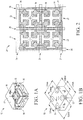
- FIG. 2 shows a portion of a lead frame array 20 used to assemble the device 10, with four individual lead frames 22 being shown.
- the lead frames 22 are separated from each other by saw streets 24, which run in the X-direction, and saw streets 26, which run in the Y-direction.
- Each of the lead frames 22 comprises four of the leads 14, which extend from the corners of the lead frames towards the centers thereof.
- the individual leads 14 extend to the corners of the frame such that each lead 14 abuts two adjacent, perpendicular saw streets.
- the lead frame array 20 may be formed from a sheet of conductive metal, such as copper, and may be pre-plated (PPF) or post-plated with Sn on either the PPF or Cu surface.
- PPF pre-plated
- the lead frame array 20 also is etched at the outer corners of the leads 14 to form dimples 28 therein.
- a dimple depth generally is one-half of the lead frame thickness following a standard lead frame half etching process.
- the leads 14 and lead frames 22 are sized and shaped to receive the die 16.
- the die 16 is mounted on and attached to the leads 14.
- the lead frames 22 may include die flags for receiving and supporting the die 16.
- Lead frame arrays formed from a sheet of copper, etching of lead frame arrays, and plating of lead frame arrays are known in the art so further description is not necessary for a complete understanding of the present invention. Referring now to FIG. 3A , a side view of the device 10 being mounted on a substrate 30 is shown.
- the substrate 30 may comprise a printed circuit board (PCB) having internal metal traces for connecting devices mounted thereon to each other, as is known in the art.
- the substrate 30 includes pads 32 to which the leads 14 of the device 10 will be electrically connected.
- FIG. 3B is an isometric view of the device 10 mounted on the substrate 30 with the leads 14 electrically connected to the substrate pads 32 with solder 34. The solder 34 contacts the leads 14 and fills the dimple 28.
- FIG. 3C is a top plan view of the device 10 attached to the substrate 30.
- FIG. 4 is a side elevational view of a packaged semiconductor device 40 in accordance with another embodiment of the present invention.
- the device 40 is similar to the device 10 and includes a body 42 formed from a mold compound that encapsulates a semiconductor die (not shown).
- the device 40 has corner leads 44 that are flush with the sides of the body 42 and are exposed at two adjacent sides and a bottom surface of the device 10.
- the device 40 also has leads 46 that are exposed on only one side and the bottom surface of the device 40. Both of the corner leads 44 and the side leads 46 include dimples 48 for receiving solder when the device 40 is attached to a substrate or circuit board.
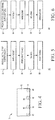
- FIG. 5 is a flow chart illustrating a method 50 of manufacturing a lead frame or an array of lead frames like the lead frame array 22 shown in FIG. 2 .
- a sheet of conductive metal such as copper is provided.
- a resist is applied to the metal sheet and then at step 56 the metal sheet is half-etched to form one or more lead frames (e.g., an array of lead frames).
- the lead frames include corner leads, like the lead frames 22 shown in FIG. 2 .
- the lead frames are separated by saw streets that extend in both the X-axis and Y-axis directions. Dimples are formed in the leads at step 56, like the dimples 28 and 48 shown in FIGS. 2 and 4 .
- a plating step 58 may be performed to plate the leads such as Pd or Ag to prevent corrosion.
- the plating step 58 can plate the entire lead frame or only selected portions thereof, as desired.
- the plating step 58 preferably is performed using an electro-plating or electro-deposition process during which the lead frames including the ends or edges of the leads 44a, 44b are coated with a solderable layer such as Nickel/Palladium/Gold.
- the leads may be connected to a source of electrical potential so that they will form a cathode during the electro-plating or electro-deposition process.
- the electro-plating or electro-deposition process results in a conductive, wettable metal layer being deposited onto the exposed surfaces of the lead frame.
- the plating layer imparts solderability or solder wettability during a soldering process such as SMT (surface mount technology) as well as protecting the exposed surfaces of the lead frame from corrosion.
- the lead frame may comprise bare copper or the lead frame may be pre-plated such as with silver at the bond surface (back side typically remains as bare copper) and a coating of tin or tin alloy may be applied to the exposed lead ends before or after cutting the lead frame into individual semiconductor devices.
- the lead frame or lead frame array is taped - that is, a layer of tape is applied the backside of the lead frame. The tape prevents the lead frames from being deformed prior to use.
- the method 50 typically is performed by a lead frame supplier. However, the method 50 also could be performed at a test and assembly facility.
- FIG. 6 is a flow chart illustrating a method 60 of assembling a semiconductor device such as the semiconductor devices 10 and 40.
- the method starts with a step 62 of being provided with a lead frame, such as the pre-plated lead frame array shown in FIG. 2 .
- the provided lead frames include dimples in the portions of the leads that will be exposed after assembly.
- a die is mounted on and attached to the leads of a lead frame, such as the lead frames made in accordance with the method 50.
- the corners of the non-active side of the die rest on and are attached to inner portions of the leads.
- a die attach adhesive or double-sided tape may be used to attach the die to the leads.
- Step 64 is followed by a wire bonding step 66, where die bonding pads are electrically connected to respective ones of the leads with bond wires.
- the die may be a flip-chip die and have solder bumps on the die bond pads and then the die is mounted on the lead frame with the die active side facing the lead frame such that the die bond pads are in direct contact with the leads.
- the wire bonding step 66 is followed by an encapsulation or molding step 68 in which the lead frame, die and bond wires are covered with a mold compound, as is known in the art.
- the molding step 68 preferably comprises a mold array process (MAP) where several assemblies formed on a lead frame array are all molded at the same time.
- MAP mold array process
- the singulated QFN (Quad Flat No lead) devices may then be inspected and packed for shipment.
Description
- The present invention relates to semiconductor packaging and, more particularly, to a semiconductor device having solder wettable corner leads or 'flanks' to facilitate inspection of solder joints when the semiconductor device is mounted on a substrate or circuit board using a surface-mount technology (SMT) process.
- A typical semiconductor device comprises a semiconductor die attached to a lead frame flag. Bonding pads on the die are electrically connected to leads of the lead frame with bond wires. This assembly is encapsulated with a mold compound, which protects the die and wire bonds from environmental and physical damage. In some packages, the leads extend outward from the sides of the package, while in others such as the Quad Flat No leads (QFN) or Dual Flat No leads (DFN), the leads are flush with the sides of the package body. For example, during assembly, an array of packages are assembled simultaneously. After the molding or encapsulation step, individual devices are formed with a saw singulation step, where adjacent devices are separated using a saw. These device are non-wettable at their flanks due to the untreated copper surface that is exposed yet flush with the side walls of the device. That is, due to the manner in which the semiconductor packages are singulated with a saw blade, the surface of the exposed lead or flank is flush with the mold compound of the device such that solder does not readily climb-up or "wick" the flank of the package meaning that the QFN package is not flank wettable. This makes it difficult to inspect the solder joints after the package has been attached to a substrate or circuit board.
- In order to overcome this deficiency, current leadless plastic packages with side solderable terminals have solderable flanks in the package side walls. However, this design cannot be applied to ultra-small packages (≤1mm x1mm) with multiple I/O terminals and a large I/O pitch (≥0.4mm) because the package is not large enough to accommodate multiple terminals in the side walls.
- Accordingly, it would be desirable to have an ultra-small leadless package with wettable flanks to facilitate inspection of solder joints when the package is mounted such as to a printed circuit board (PCB) using an SMT process.
-
US2011074016 relates to a semiconductor package with a flip chip bonding structure which includes: a semiconductor chip having a main surface with multiple electrode pads formed therein and a back surface located on the opposite side thereto;
four lead terminals each having an upper surface with the semiconductor chip placed thereover and a lower surface located on the opposite side thereto;
and a sealing body having a main surface and a back surface located on the opposite side thereto. -
JP2003258187 - The following detailed description of a preferred embodiment of the invention will be better understood when read in conjunction with the appended drawings. The present invention is illustrated by way of example and is not limited by the accompanying figures in which like references indicate similar elements. It is to be understood that the drawings are not to scale and have been simplified for ease of understanding the invention.
-
FIGS. 1A and 1B are a see-through front isometric view, and a bottom isometric view of a semiconductor device in accordance with an embodiment of the present invention; -
FIG. 2 is a top plan view of a lead frame array used to assemble the device ofFIGS. 1A - 1B ; -
FIGS. 3A, 3B and 3C are a front elevational view, a top plan view, and a side view illustrating the device ofFIGS. 1A - 1C being attached to a substrate; -
FIG. 4 is a side elevational view of a semiconductor device in accordance with another embodiment of the invention; -
FIG. 5 is a flow chart illustrating a method of manufacturing a lead frame in accordance with an embodiment of the invention; and -
FIG. 6 is a flow chart illustrating a method of assembling a semiconductor device in accordance with an embodiment of the present invention. - In one embodiment, the present invention provides a method of assembling a flank wettable semiconductor device. The method includes providing an array of rectangular lead frames, wherein individual lead frames are separated by saw streets and each lead frame has leads that extend to corners of the lead frame such that each lead has an end that abuts two adjacent, perpendicular saw streets. The lead frame is etched along the saw streets such that dimples are formed at the end of each of the leads. Semiconductor dies are mounted on and attached to respective ones of the lead frames. Then, bond pads on the dies are electrically connected with respective ones of the leads of the lead frames upon which the dies are mounted. The dies and the electrical connections are encapsulated with a mold compound and then the lead frame array is cut along the saw streets to separate individual devices from adjacent devices. Each device has corner bond pads that are flush with the mold compound and the dimples of each lead are exposed after the cutting.
- In another embodiment the present invention provides a flank wettable semiconductor device. The device comprises a lead frame including a plurality of leads, and a semiconductor die mounted on the lead frame. Bonding pads on the die are electrically connected to respective ones of the leads. A mold compound encapsulates the die, the leads and the electrical connections. Ends of the leads are exposed at corner side walls of the device. The exposed portion of each of the leads is flush with two adjacent sides of the device, and includes a dimple therein such that the leads are wettable.
- Referring now to
FIGS. 1A and 1B , asemiconductor device 10 in accordance with a preferred embodiment of the present invention is shown.FIG. 1A is a see-through front isometric view, andFIG. 1B is a bottom isometric view of thesemiconductor device 10. Thedevice 10 is generally rectangular in shape and also is generally very small. For example, in one embodiment thedevice 10 is on the order of 0.6mm X 0.6mm (L X W). - The
device 10 has abody 12 formed from a mold compound and four leads 14. Thebody 12, in this embodiment, is generally square shaped and theleads 14 are exposed at the four corners of the bottom and side surfaces of thedevice 10. Theleads 14 also are flush with the bottom and side surfaces of thedevice 10 and include a dimple at the corner, which facilitates wicking of solder when thedevice 10 is attached to a substrate or circuit board (not shown). In one embodiment, theleads 14 are spaced from each other by about 0.4mm. - As can be seen in
FIG. 1A , thedevice 10 also comprises asemiconductor die 16 that is mounted on and attached to theleads 14. Bonding pads of the die 16 are electrically connected to theleads 14, in this embodiment, withbond wires 18. In other embodiments, the die 16 could comprise a flip-chip die having bumps on its bonding pads such that the die can be electrically connected to theleads 14 by placing the die bonding pads in contact with theleads 14. The die 16,bond wires 18, and portions of theleads 14 are encapsulated by themold compound 12. -
FIG. 2 shows a portion of alead frame array 20 used to assemble thedevice 10, with fourindividual lead frames 22 being shown. Thelead frames 22 are separated from each other by sawstreets 24, which run in the X-direction, and sawstreets 26, which run in the Y-direction. Each of thelead frames 22 comprises four of theleads 14, which extend from the corners of the lead frames towards the centers thereof. At thesaw streets lead frame array 20 may be formed from a sheet of conductive metal, such as copper, and may be pre-plated (PPF) or post-plated with Sn on either the PPF or Cu surface. Thelead frame array 20 also is etched at the outer corners of theleads 14 to formdimples 28 therein. A dimple depth generally is one-half of the lead frame thickness following a standard lead frame half etching process. The leads 14 and leadframes 22 are sized and shaped to receive thedie 16. In the embodiment shown thedie 16 is mounted on and attached to the leads 14. In other embodiments, the lead frames 22 may include die flags for receiving and supporting thedie 16. Lead frame arrays formed from a sheet of copper, etching of lead frame arrays, and plating of lead frame arrays are known in the art so further description is not necessary for a complete understanding of the present invention. Referring now toFIG. 3A , a side view of thedevice 10 being mounted on asubstrate 30 is shown. Thesubstrate 30 may comprise a printed circuit board (PCB) having internal metal traces for connecting devices mounted thereon to each other, as is known in the art. Thesubstrate 30 includespads 32 to which the leads 14 of thedevice 10 will be electrically connected.FIG. 3B is an isometric view of thedevice 10 mounted on thesubstrate 30 with theleads 14 electrically connected to thesubstrate pads 32 withsolder 34. Thesolder 34 contacts theleads 14 and fills thedimple 28.FIG. 3C is a top plan view of thedevice 10 attached to thesubstrate 30. - As can be seen, it is relatively easy to visually inspect the solder joints that couple the
device 10 to thesubstrate 30. -
FIG. 4 is a side elevational view of a packaged semiconductor device 40 in accordance with another embodiment of the present invention. The device 40 is similar to thedevice 10 and includes abody 42 formed from a mold compound that encapsulates a semiconductor die (not shown). The device 40 has corner leads 44 that are flush with the sides of thebody 42 and are exposed at two adjacent sides and a bottom surface of thedevice 10. The device 40 also has leads 46 that are exposed on only one side and the bottom surface of the device 40. Both of the corner leads 44 and the side leads 46 includedimples 48 for receiving solder when the device 40 is attached to a substrate or circuit board. -
FIG. 5 is a flow chart illustrating amethod 50 of manufacturing a lead frame or an array of lead frames like thelead frame array 22 shown inFIG. 2 . - At
step 52, a sheet of conductive metal, such as copper is provided. Atstep 54, a resist is applied to the metal sheet and then atstep 56 the metal sheet is half-etched to form one or more lead frames (e.g., an array of lead frames). In accordance with the present invention, the lead frames include corner leads, like the lead frames 22 shown inFIG. 2 . The lead frames are separated by saw streets that extend in both the X-axis and Y-axis directions. Dimples are formed in the leads atstep 56, like thedimples FIGS. 2 and4 . After the lead frames have been half-etched, aplating step 58 may be performed to plate the leads such as Pd or Ag to prevent corrosion. The platingstep 58 can plate the entire lead frame or only selected portions thereof, as desired. The platingstep 58 preferably is performed using an electro-plating or electro-deposition process during which the lead frames including the ends or edges of the leads 44a, 44b are coated with a solderable layer such as Nickel/Palladium/Gold. During the plating process, the leads may be connected to a source of electrical potential so that they will form a cathode during the electro-plating or electro-deposition process. The electro-plating or electro-deposition process results in a conductive, wettable metal layer being deposited onto the exposed surfaces of the lead frame. The plating layer imparts solderability or solder wettability during a soldering process such as SMT (surface mount technology) as well as protecting the exposed surfaces of the lead frame from corrosion. It should be noted that the lead frame may comprise bare copper or the lead frame may be pre-plated such as with silver at the bond surface (back side typically remains as bare copper) and a coating of tin or tin alloy may be applied to the exposed lead ends before or after cutting the lead frame into individual semiconductor devices. Atstep 59, the lead frame or lead frame array is taped - that is, a layer of tape is applied the backside of the lead frame. The tape prevents the lead frames from being deformed prior to use. Themethod 50 typically is performed by a lead frame supplier. However, themethod 50 also could be performed at a test and assembly facility. -
FIG. 6 is a flow chart illustrating amethod 60 of assembling a semiconductor device such as thesemiconductor devices 10 and 40. - The method starts with a
step 62 of being provided with a lead frame, such as the pre-plated lead frame array shown inFIG. 2 . The provided lead frames include dimples in the portions of the leads that will be exposed after assembly. At step 64 a die is mounted on and attached to the leads of a lead frame, such as the lead frames made in accordance with themethod 50. In a presently preferred embodiment, the corners of the non-active side of the die rest on and are attached to inner portions of the leads. A die attach adhesive or double-sided tape may be used to attach the die to the leads. -
Step 64 is followed by awire bonding step 66, where die bonding pads are electrically connected to respective ones of the leads with bond wires. In an alternative embodiment, the die may be a flip-chip die and have solder bumps on the die bond pads and then the die is mounted on the lead frame with the die active side facing the lead frame such that the die bond pads are in direct contact with the leads. - The
wire bonding step 66 is followed by an encapsulation ormolding step 68 in which the lead frame, die and bond wires are covered with a mold compound, as is known in the art. Themolding step 68 preferably comprises a mold array process (MAP) where several assemblies formed on a lead frame array are all molded at the same time. After themolding step 68, laser marking is performed and if there is a tape on a bottom surface of the lead frame array, then the tape is removed in a de-taping step. Then the assemblies are separated from each other in asingulation step 69 in which a saw blade is run along the saw streets, thereby cutting and separating the simultaneously assembled devices from each other. The singulated QFN (Quad Flat No lead) devices may then be inspected and packed for shipment.
Claims (13)
- A method of assembling a flank wettable semiconductor device, comprising:providing an array of rectangular lead frames, wherein individual lead frames are separated by saw streets and each lead frame has leads that extend to corners of the lead frame such that each corner lead has an end that abuts two adjacent, perpendicular saw streets, and wherein each corner lead has a dimple formed at an outer surface thereof;mounting and attaching semiconductor dies to respective ones of the lead frames;electrically connecting bond pads on the dies with respective ones of the leads of the lead frames upon which the dies are mounted;encapsulating the dies and the electrical connections with a mold compound;cutting the lead frame array along the saw streets to separate individual devices from adjacent devices, whereby each device has corner bond pads that are flush with the mold compound thereof and wherein the dimples of each corner lead are exposed after the cutting.
- The method of claim 1, further comprising applying a coating metal or metal alloy to the exposed lead ends prior to cutting the lead frame into individual semiconductor devices.
- The method of claim 2, wherein the metal coating is applied by electro-plating or electro-deposition.
- The method of claim 3, wherein the coating metal or metal alloy comprises tin or a tin alloy.
- The method of any preceding claim, wherein the step of electrically connecting comprises attaching bond wires to the die bonding pads and respective ones of the leads.
- The method of any preceding claim, wherein non-active sides of the dies are attached to the leads of each of the respective lead frames.
- The method of any preceding claim, wherein each individual lead frame has four corner leads, each of which extends to a separate corner thereof.
- The method of claim 7, wherein each individual lead frame includes one or more additional leads disposed on a side of the semiconductor device between the corner leads on said side.
- A flank wettable semiconductor device, comprising:a lead frame including a plurality of leads;a semiconductor die mounted on the lead frame, wherein bonding pads on the die are electrically connected to respective ones of the leads;a mold compound that encapsulates the die, the leads and the electrical connections, wherein ends of the leads are exposed at corner side walls of the device, andwherein the exposed portion of each of the leads is flush with two adjacent sides of the device, and includes a dimple therein such that the leads are wettable.
- The semiconductor device of claim 9, further comprising a coating of a protective metal or metal alloy on the exposed portions of the leads.
- The semiconductor device of claim 10, wherein the coating comprises a tin or tin alloy.
- The semiconductor device of claims 9 to 11, wherein the coating is applied to the exposed portions of the leads by electro-plating or electro-deposition prior to the device being separated from an adjacent device during assembly.
- The semiconductor device of claims 9 to 12, further comprising a plurality of bond wires that electrically connect the die bonding pads with the leads.
Applications Claiming Priority (1)
| Application Number | Priority Date | Filing Date | Title |
|---|---|---|---|
| US15/344,564 US9847283B1 (en) | 2016-11-06 | 2016-11-06 | Semiconductor device with wettable corner leads |
Publications (2)
| Publication Number | Publication Date |
|---|---|
| EP3319122A1 EP3319122A1 (en) | 2018-05-09 |
| EP3319122B1 true EP3319122B1 (en) | 2019-06-26 |
Family
ID=59846445
Family Applications (1)
| Application Number | Title | Priority Date | Filing Date |
|---|---|---|---|
| EP17190245.5A Active EP3319122B1 (en) | 2016-11-06 | 2017-09-08 | Semiconductor device with wettable corner leads |
Country Status (3)
| Country | Link |
|---|---|
| US (1) | US9847283B1 (en) |
| EP (1) | EP3319122B1 (en) |
| CN (1) | CN108074901B (en) |
Cited By (2)
| Publication number | Priority date | Publication date | Assignee | Title |
|---|---|---|---|---|
| US11393699B2 (en) | 2019-12-24 | 2022-07-19 | Vishay General Semiconductor, Llc | Packaging process for plating with selective molding |
| US11450534B2 (en) | 2019-12-24 | 2022-09-20 | Vishay General Semiconductor, Llc | Packaging process for side-wall plating with a conductive film |
Family Cites Families (36)
| Publication number | Priority date | Publication date | Assignee | Title |
|---|---|---|---|---|
| US5804880A (en) | 1996-11-04 | 1998-09-08 | National Semiconductor Corporation | Solder isolating lead frame |
| US6544817B2 (en) | 2000-06-23 | 2003-04-08 | Carsem Semiconductor Sdn. Bhd. | Method for sawing a moulded leadframe package |
| JP3660861B2 (en) * | 2000-08-18 | 2005-06-15 | 株式会社ルネサステクノロジ | Manufacturing method of semiconductor device |
| US20020177254A1 (en) | 2000-10-31 | 2002-11-28 | Chow Wai Wong | Semiconductor package and method for making the same |
| JP2002164470A (en) * | 2000-11-27 | 2002-06-07 | Hitachi Ltd | Semiconductor device and its manufacturing method |
| JP3895570B2 (en) | 2000-12-28 | 2007-03-22 | 株式会社ルネサステクノロジ | Semiconductor device |
| JP4034073B2 (en) | 2001-05-11 | 2008-01-16 | 株式会社ルネサステクノロジ | Manufacturing method of semiconductor device |
| JP2003110080A (en) * | 2001-09-28 | 2003-04-11 | Citizen Electronics Co Ltd | Semiconductor device |
| JP2003174137A (en) * | 2001-12-06 | 2003-06-20 | Citizen Electronics Co Ltd | Semiconductor device and method for manufacturing the same |
| DE10202881B4 (en) | 2002-01-25 | 2007-09-20 | Infineon Technologies Ag | Method for producing semiconductor chips with a chip edge protection layer, in particular for wafer level packaging chips |
| JP2003258187A (en) * | 2002-03-01 | 2003-09-12 | Citizen Electronics Co Ltd | Semiconductor device |
| US6885086B1 (en) | 2002-03-05 | 2005-04-26 | Amkor Technology, Inc. | Reduced copper lead frame for saw-singulated chip package |
| US6608366B1 (en) | 2002-04-15 | 2003-08-19 | Harry J. Fogelson | Lead frame with plated end leads |
| JP2004055860A (en) | 2002-07-22 | 2004-02-19 | Renesas Technology Corp | Semiconductor device fabricating process |
| US6872599B1 (en) | 2002-12-10 | 2005-03-29 | National Semiconductor Corporation | Enhanced solder joint strength and ease of inspection of leadless leadframe package (LLP) |
| US7060535B1 (en) | 2003-10-29 | 2006-06-13 | Ns Electronics Bangkok (1993) Ltd. | Flat no-lead semiconductor die package including stud terminals |
| JP2005191240A (en) | 2003-12-25 | 2005-07-14 | Renesas Technology Corp | Semiconductor device and method for manufacturing the same |
| JP4417150B2 (en) * | 2004-03-23 | 2010-02-17 | 株式会社ルネサステクノロジ | Semiconductor device |
| CN100440444C (en) | 2004-07-22 | 2008-12-03 | 株式会社瑞萨科技 | Semiconductor device manufacturing method |
| WO2009125250A1 (en) | 2008-04-11 | 2009-10-15 | Freescale Semiconductor, Inc. | Integrated circuit package, method of manufacturing an integrated circuit package and printed circuit board |
| JP2009294719A (en) | 2008-06-02 | 2009-12-17 | Autonetworks Technologies Ltd | Road marking recognition device |
| US8652881B2 (en) | 2008-09-22 | 2014-02-18 | Stats Chippac Ltd. | Integrated circuit package system with anti-peel contact pads |
| US20100133693A1 (en) * | 2008-12-03 | 2010-06-03 | Texas Instruments Incorporated | Semiconductor Package Leads Having Grooved Contact Areas |
| JP5271949B2 (en) * | 2009-09-29 | 2013-08-21 | ルネサスエレクトロニクス株式会社 | Semiconductor device |
| US8501539B2 (en) * | 2009-11-12 | 2013-08-06 | Freescale Semiconductor, Inc. | Semiconductor device package |
| US20110140253A1 (en) * | 2009-12-14 | 2011-06-16 | National Semiconductor Corporation | Dap ground bond enhancement |
| US8329509B2 (en) | 2010-04-01 | 2012-12-11 | Freescale Semiconductor, Inc. | Packaging process to create wettable lead flank during board assembly |
| US8017447B1 (en) * | 2010-08-03 | 2011-09-13 | Linear Technology Corporation | Laser process for side plating of terminals |
| CN103155136B (en) | 2010-09-29 | 2015-03-04 | Nxp股份有限公司 | Singulation of IC packages |
| US20120126378A1 (en) * | 2010-11-24 | 2012-05-24 | Unisem (Mauritius ) Holdings Limited | Semiconductor device package with electromagnetic shielding |
| CN102789994B (en) | 2011-05-18 | 2016-08-10 | 飞思卡尔半导体公司 | The wettable semiconductor device in side |
| US8841758B2 (en) * | 2012-06-29 | 2014-09-23 | Freescale Semiconductor, Inc. | Semiconductor device package and method of manufacture |
| JP6244147B2 (en) | 2013-09-18 | 2017-12-06 | エスアイアイ・セミコンダクタ株式会社 | Manufacturing method of semiconductor device |
| US9892952B2 (en) | 2014-07-25 | 2018-02-13 | Semiconductor Components Industries, Llc | Wafer level flat no-lead semiconductor packages and methods of manufacture |
| US20160148876A1 (en) * | 2014-11-20 | 2016-05-26 | Microchip Technology Incorporated | Flat no-leads package with improved contact pins |
| US9578744B2 (en) * | 2014-12-22 | 2017-02-21 | Stmicroelectronics, Inc. | Leadframe package with pre-applied filler material |
-
2016
- 2016-11-06 US US15/344,564 patent/US9847283B1/en active Active
-
2017
- 2017-09-08 EP EP17190245.5A patent/EP3319122B1/en active Active
- 2017-11-06 CN CN201711078780.1A patent/CN108074901B/en active Active
Non-Patent Citations (1)
| Title |
|---|
| None * |
Cited By (4)
| Publication number | Priority date | Publication date | Assignee | Title |
|---|---|---|---|---|
| US11393699B2 (en) | 2019-12-24 | 2022-07-19 | Vishay General Semiconductor, Llc | Packaging process for plating with selective molding |
| US11450534B2 (en) | 2019-12-24 | 2022-09-20 | Vishay General Semiconductor, Llc | Packaging process for side-wall plating with a conductive film |
| US11764075B2 (en) | 2019-12-24 | 2023-09-19 | Vishay General Semiconductor, Llc | Package assembly for plating with selective molding |
| US11876003B2 (en) | 2019-12-24 | 2024-01-16 | Vishay General Semiconductor, Llc | Semiconductor package and packaging process for side-wall plating with a conductive film |
Also Published As
| Publication number | Publication date |
|---|---|
| CN108074901A (en) | 2018-05-25 |
| CN108074901B (en) | 2023-11-03 |
| EP3319122A1 (en) | 2018-05-09 |
| US9847283B1 (en) | 2017-12-19 |
Similar Documents
| Publication | Publication Date | Title |
|---|---|---|
| US8685795B2 (en) | Flank wettable semiconductor device | |
| KR102054385B1 (en) | Resin-encapsulated semiconductor device and method of manufacturing the same | |
| US6525406B1 (en) | Semiconductor device having increased moisture path and increased solder joint strength | |
| US20160056097A1 (en) | Semiconductor device with inspectable solder joints | |
| US7808084B1 (en) | Semiconductor package with half-etched locking features | |
| US20080265396A1 (en) | Quad flat no-lead chip carrier with standoff | |
| US20030006055A1 (en) | Semiconductor package for fixed surface mounting | |
| US20050087847A1 (en) | Method for fabricating a semiconductor package with multi layered leadframe | |
| CN209785926U (en) | semiconductor device with a plurality of transistors | |
| JP2005057067A (en) | Semiconductor device and manufacturing method thereof | |
| US11342252B2 (en) | Leadframe leads having fully plated end faces | |
| US9177836B1 (en) | Packaged integrated circuit device having bent leads | |
| US8115288B2 (en) | Lead frame for semiconductor device | |
| KR20150109284A (en) | Semiconductor device and method of manufacturing the same | |
| KR20150105923A (en) | Semiconductor device and method of manufacturing the same | |
| CN212182312U (en) | Semiconductor package | |
| KR100804341B1 (en) | A semiconductor device and method of manufacturing the same | |
| EP3319122B1 (en) | Semiconductor device with wettable corner leads | |
| US20110108967A1 (en) | Semiconductor chip grid array package and method for fabricating same | |
| US20200321228A1 (en) | Method of manufacturing a lead frame, method of manufacturing an electronic apparatus, and electronic apparatus | |
| US20220208660A1 (en) | Electronic package with surface contact wire extensions | |
| US11227820B2 (en) | Through hole side wettable flank | |
| US9099363B1 (en) | Substrate with corner cut-outs and semiconductor device assembled therewith | |
| US20190067033A1 (en) | Surface Mount Semiconductor Device and Method of Manufacture | |
| US20210183752A1 (en) | Semiconductor device and corresponding method |
Legal Events
| Date | Code | Title | Description |
|---|---|---|---|
| PUAI | Public reference made under article 153(3) epc to a published international application that has entered the european phase |
Free format text: ORIGINAL CODE: 0009012 |
|
| STAA | Information on the status of an ep patent application or granted ep patent |
Free format text: STATUS: THE APPLICATION HAS BEEN PUBLISHED |
|
| AK | Designated contracting states |
Kind code of ref document: A1 Designated state(s): AL AT BE BG CH CY CZ DE DK EE ES FI FR GB GR HR HU IE IS IT LI LT LU LV MC MK MT NL NO PL PT RO RS SE SI SK SM TR |
|
| AX | Request for extension of the european patent |
Extension state: BA ME |
|
| STAA | Information on the status of an ep patent application or granted ep patent |
Free format text: STATUS: REQUEST FOR EXAMINATION WAS MADE |
|
| 17P | Request for examination filed |
Effective date: 20181101 |
|
| RBV | Designated contracting states (corrected) |
Designated state(s): AL AT BE BG CH CY CZ DE DK EE ES FI FR GB GR HR HU IE IS IT LI LT LU LV MC MK MT NL NO PL PT RO RS SE SI SK SM TR |
|
| GRAP | Despatch of communication of intention to grant a patent |
Free format text: ORIGINAL CODE: EPIDOSNIGR1 |
|
| STAA | Information on the status of an ep patent application or granted ep patent |
Free format text: STATUS: GRANT OF PATENT IS INTENDED |
|
| INTG | Intention to grant announced |
Effective date: 20190313 |
|
| GRAS | Grant fee paid |
Free format text: ORIGINAL CODE: EPIDOSNIGR3 |
|
| GRAA | (expected) grant |
Free format text: ORIGINAL CODE: 0009210 |
|
| STAA | Information on the status of an ep patent application or granted ep patent |
Free format text: STATUS: THE PATENT HAS BEEN GRANTED |
|
| AK | Designated contracting states |
Kind code of ref document: B1 Designated state(s): AL AT BE BG CH CY CZ DE DK EE ES FI FR GB GR HR HU IE IS IT LI LT LU LV MC MK MT NL NO PL PT RO RS SE SI SK SM TR |
|
| REG | Reference to a national code |
Ref country code: GB Ref legal event code: FG4D |
|
| REG | Reference to a national code |
Ref country code: CH Ref legal event code: EP |
|
| REG | Reference to a national code |
Ref country code: AT Ref legal event code: REF Ref document number: 1149293 Country of ref document: AT Kind code of ref document: T Effective date: 20190715 |
|
| REG | Reference to a national code |
Ref country code: DE Ref legal event code: R096 Ref document number: 602017004812 Country of ref document: DE |
|
| REG | Reference to a national code |
Ref country code: IE Ref legal event code: FG4D |
|
| REG | Reference to a national code |
Ref country code: NL Ref legal event code: MP Effective date: 20190626 |
|
| PG25 | Lapsed in a contracting state [announced via postgrant information from national office to epo] |
Ref country code: SE Free format text: LAPSE BECAUSE OF FAILURE TO SUBMIT A TRANSLATION OF THE DESCRIPTION OR TO PAY THE FEE WITHIN THE PRESCRIBED TIME-LIMIT Effective date: 20190626 Ref country code: HR Free format text: LAPSE BECAUSE OF FAILURE TO SUBMIT A TRANSLATION OF THE DESCRIPTION OR TO PAY THE FEE WITHIN THE PRESCRIBED TIME-LIMIT Effective date: 20190626 Ref country code: AL Free format text: LAPSE BECAUSE OF FAILURE TO SUBMIT A TRANSLATION OF THE DESCRIPTION OR TO PAY THE FEE WITHIN THE PRESCRIBED TIME-LIMIT Effective date: 20190626 Ref country code: FI Free format text: LAPSE BECAUSE OF FAILURE TO SUBMIT A TRANSLATION OF THE DESCRIPTION OR TO PAY THE FEE WITHIN THE PRESCRIBED TIME-LIMIT Effective date: 20190626 Ref country code: NO Free format text: LAPSE BECAUSE OF FAILURE TO SUBMIT A TRANSLATION OF THE DESCRIPTION OR TO PAY THE FEE WITHIN THE PRESCRIBED TIME-LIMIT Effective date: 20190926 Ref country code: LT Free format text: LAPSE BECAUSE OF FAILURE TO SUBMIT A TRANSLATION OF THE DESCRIPTION OR TO PAY THE FEE WITHIN THE PRESCRIBED TIME-LIMIT Effective date: 20190626 |
|
| REG | Reference to a national code |
Ref country code: LT Ref legal event code: MG4D |
|
| PG25 | Lapsed in a contracting state [announced via postgrant information from national office to epo] |
Ref country code: GR Free format text: LAPSE BECAUSE OF FAILURE TO SUBMIT A TRANSLATION OF THE DESCRIPTION OR TO PAY THE FEE WITHIN THE PRESCRIBED TIME-LIMIT Effective date: 20190927 Ref country code: RS Free format text: LAPSE BECAUSE OF FAILURE TO SUBMIT A TRANSLATION OF THE DESCRIPTION OR TO PAY THE FEE WITHIN THE PRESCRIBED TIME-LIMIT Effective date: 20190626 Ref country code: BG Free format text: LAPSE BECAUSE OF FAILURE TO SUBMIT A TRANSLATION OF THE DESCRIPTION OR TO PAY THE FEE WITHIN THE PRESCRIBED TIME-LIMIT Effective date: 20190926 Ref country code: LV Free format text: LAPSE BECAUSE OF FAILURE TO SUBMIT A TRANSLATION OF THE DESCRIPTION OR TO PAY THE FEE WITHIN THE PRESCRIBED TIME-LIMIT Effective date: 20190626 |
|
| REG | Reference to a national code |
Ref country code: AT Ref legal event code: MK05 Ref document number: 1149293 Country of ref document: AT Kind code of ref document: T Effective date: 20190626 |
|
| PG25 | Lapsed in a contracting state [announced via postgrant information from national office to epo] |
Ref country code: NL Free format text: LAPSE BECAUSE OF FAILURE TO SUBMIT A TRANSLATION OF THE DESCRIPTION OR TO PAY THE FEE WITHIN THE PRESCRIBED TIME-LIMIT Effective date: 20190626 Ref country code: AT Free format text: LAPSE BECAUSE OF FAILURE TO SUBMIT A TRANSLATION OF THE DESCRIPTION OR TO PAY THE FEE WITHIN THE PRESCRIBED TIME-LIMIT Effective date: 20190626 Ref country code: EE Free format text: LAPSE BECAUSE OF FAILURE TO SUBMIT A TRANSLATION OF THE DESCRIPTION OR TO PAY THE FEE WITHIN THE PRESCRIBED TIME-LIMIT Effective date: 20190626 Ref country code: CZ Free format text: LAPSE BECAUSE OF FAILURE TO SUBMIT A TRANSLATION OF THE DESCRIPTION OR TO PAY THE FEE WITHIN THE PRESCRIBED TIME-LIMIT Effective date: 20190626 Ref country code: RO Free format text: LAPSE BECAUSE OF FAILURE TO SUBMIT A TRANSLATION OF THE DESCRIPTION OR TO PAY THE FEE WITHIN THE PRESCRIBED TIME-LIMIT Effective date: 20190626 Ref country code: SK Free format text: LAPSE BECAUSE OF FAILURE TO SUBMIT A TRANSLATION OF THE DESCRIPTION OR TO PAY THE FEE WITHIN THE PRESCRIBED TIME-LIMIT Effective date: 20190626 Ref country code: PT Free format text: LAPSE BECAUSE OF FAILURE TO SUBMIT A TRANSLATION OF THE DESCRIPTION OR TO PAY THE FEE WITHIN THE PRESCRIBED TIME-LIMIT Effective date: 20191028 |
|
| PG25 | Lapsed in a contracting state [announced via postgrant information from national office to epo] |
Ref country code: IS Free format text: LAPSE BECAUSE OF FAILURE TO SUBMIT A TRANSLATION OF THE DESCRIPTION OR TO PAY THE FEE WITHIN THE PRESCRIBED TIME-LIMIT Effective date: 20191026 Ref country code: SM Free format text: LAPSE BECAUSE OF FAILURE TO SUBMIT A TRANSLATION OF THE DESCRIPTION OR TO PAY THE FEE WITHIN THE PRESCRIBED TIME-LIMIT Effective date: 20190626 Ref country code: IT Free format text: LAPSE BECAUSE OF FAILURE TO SUBMIT A TRANSLATION OF THE DESCRIPTION OR TO PAY THE FEE WITHIN THE PRESCRIBED TIME-LIMIT Effective date: 20190626 Ref country code: ES Free format text: LAPSE BECAUSE OF FAILURE TO SUBMIT A TRANSLATION OF THE DESCRIPTION OR TO PAY THE FEE WITHIN THE PRESCRIBED TIME-LIMIT Effective date: 20190626 |
|
| PG25 | Lapsed in a contracting state [announced via postgrant information from national office to epo] |
Ref country code: TR Free format text: LAPSE BECAUSE OF FAILURE TO SUBMIT A TRANSLATION OF THE DESCRIPTION OR TO PAY THE FEE WITHIN THE PRESCRIBED TIME-LIMIT Effective date: 20190626 |
|
| PG25 | Lapsed in a contracting state [announced via postgrant information from national office to epo] |
Ref country code: DK Free format text: LAPSE BECAUSE OF FAILURE TO SUBMIT A TRANSLATION OF THE DESCRIPTION OR TO PAY THE FEE WITHIN THE PRESCRIBED TIME-LIMIT Effective date: 20190626 Ref country code: PL Free format text: LAPSE BECAUSE OF FAILURE TO SUBMIT A TRANSLATION OF THE DESCRIPTION OR TO PAY THE FEE WITHIN THE PRESCRIBED TIME-LIMIT Effective date: 20190626 |
|
| PG25 | Lapsed in a contracting state [announced via postgrant information from national office to epo] |
Ref country code: IS Free format text: LAPSE BECAUSE OF FAILURE TO SUBMIT A TRANSLATION OF THE DESCRIPTION OR TO PAY THE FEE WITHIN THE PRESCRIBED TIME-LIMIT Effective date: 20200320 Ref country code: MC Free format text: LAPSE BECAUSE OF FAILURE TO SUBMIT A TRANSLATION OF THE DESCRIPTION OR TO PAY THE FEE WITHIN THE PRESCRIBED TIME-LIMIT Effective date: 20190626 |
|
| REG | Reference to a national code |
Ref country code: DE Ref legal event code: R097 Ref document number: 602017004812 Country of ref document: DE |
|
| PLBE | No opposition filed within time limit |
Free format text: ORIGINAL CODE: 0009261 |
|
| STAA | Information on the status of an ep patent application or granted ep patent |
Free format text: STATUS: NO OPPOSITION FILED WITHIN TIME LIMIT |
|
| PG2D | Information on lapse in contracting state deleted |
Ref country code: IS |
|
| PG25 | Lapsed in a contracting state [announced via postgrant information from national office to epo] |
Ref country code: IE Free format text: LAPSE BECAUSE OF NON-PAYMENT OF DUE FEES Effective date: 20190908 Ref country code: LU Free format text: LAPSE BECAUSE OF NON-PAYMENT OF DUE FEES Effective date: 20190908 |
|
| REG | Reference to a national code |
Ref country code: BE Ref legal event code: MM Effective date: 20190930 |
|
| 26N | No opposition filed |
Effective date: 20200603 |
|
| PG25 | Lapsed in a contracting state [announced via postgrant information from national office to epo] |
Ref country code: SI Free format text: LAPSE BECAUSE OF FAILURE TO SUBMIT A TRANSLATION OF THE DESCRIPTION OR TO PAY THE FEE WITHIN THE PRESCRIBED TIME-LIMIT Effective date: 20190626 Ref country code: BE Free format text: LAPSE BECAUSE OF NON-PAYMENT OF DUE FEES Effective date: 20190930 |
|
| PG25 | Lapsed in a contracting state [announced via postgrant information from national office to epo] |
Ref country code: FR Free format text: LAPSE BECAUSE OF NON-PAYMENT OF DUE FEES Effective date: 20190930 |
|
| REG | Reference to a national code |
Ref country code: CH Ref legal event code: PL |
|
| PG25 | Lapsed in a contracting state [announced via postgrant information from national office to epo] |
Ref country code: CY Free format text: LAPSE BECAUSE OF FAILURE TO SUBMIT A TRANSLATION OF THE DESCRIPTION OR TO PAY THE FEE WITHIN THE PRESCRIBED TIME-LIMIT Effective date: 20190626 |
|
| PG25 | Lapsed in a contracting state [announced via postgrant information from national office to epo] |
Ref country code: HU Free format text: LAPSE BECAUSE OF FAILURE TO SUBMIT A TRANSLATION OF THE DESCRIPTION OR TO PAY THE FEE WITHIN THE PRESCRIBED TIME-LIMIT; INVALID AB INITIO Effective date: 20170908 Ref country code: MT Free format text: LAPSE BECAUSE OF FAILURE TO SUBMIT A TRANSLATION OF THE DESCRIPTION OR TO PAY THE FEE WITHIN THE PRESCRIBED TIME-LIMIT Effective date: 20190626 |
|
| PG25 | Lapsed in a contracting state [announced via postgrant information from national office to epo] |
Ref country code: CH Free format text: LAPSE BECAUSE OF NON-PAYMENT OF DUE FEES Effective date: 20200930 Ref country code: LI Free format text: LAPSE BECAUSE OF NON-PAYMENT OF DUE FEES Effective date: 20200930 |
|
| GBPC | Gb: european patent ceased through non-payment of renewal fee |
Effective date: 20210908 |
|
| PG25 | Lapsed in a contracting state [announced via postgrant information from national office to epo] |
Ref country code: MK Free format text: LAPSE BECAUSE OF FAILURE TO SUBMIT A TRANSLATION OF THE DESCRIPTION OR TO PAY THE FEE WITHIN THE PRESCRIBED TIME-LIMIT Effective date: 20190626 |
|
| PG25 | Lapsed in a contracting state [announced via postgrant information from national office to epo] |
Ref country code: GB Free format text: LAPSE BECAUSE OF NON-PAYMENT OF DUE FEES Effective date: 20210908 |
|
| PGFP | Annual fee paid to national office [announced via postgrant information from national office to epo] |
Ref country code: DE Payment date: 20230928 Year of fee payment: 7 |