JP2004228342A - Semiconductor device and its manufacturing method - Google Patents
Semiconductor device and its manufacturing method Download PDFInfo
- Publication number
- JP2004228342A JP2004228342A JP2003014466A JP2003014466A JP2004228342A JP 2004228342 A JP2004228342 A JP 2004228342A JP 2003014466 A JP2003014466 A JP 2003014466A JP 2003014466 A JP2003014466 A JP 2003014466A JP 2004228342 A JP2004228342 A JP 2004228342A
- Authority
- JP
- Japan
- Prior art keywords
- film
- trench
- oxide film
- silicon oxide
- boron
- Prior art date
- Legal status (The legal status is an assumption and is not a legal conclusion. Google has not performed a legal analysis and makes no representation as to the accuracy of the status listed.)
- Pending
Links
- 239000004065 semiconductor Substances 0.000 title claims abstract description 45
- 238000004519 manufacturing process Methods 0.000 title claims abstract description 16
- 229910052581 Si3N4 Inorganic materials 0.000 claims abstract description 42
- HQVNEWCFYHHQES-UHFFFAOYSA-N silicon nitride Chemical compound N12[Si]34N5[Si]62N3[Si]51N64 HQVNEWCFYHHQES-UHFFFAOYSA-N 0.000 claims abstract description 42
- ZOXJGFHDIHLPTG-UHFFFAOYSA-N Boron Chemical compound [B] ZOXJGFHDIHLPTG-UHFFFAOYSA-N 0.000 claims abstract description 32
- 229910052796 boron Inorganic materials 0.000 claims abstract description 32
- 229910021420 polycrystalline silicon Inorganic materials 0.000 claims abstract description 21
- 229920005591 polysilicon Polymers 0.000 claims abstract description 20
- VYPSYNLAJGMNEJ-UHFFFAOYSA-N Silicium dioxide Chemical compound O=[Si]=O VYPSYNLAJGMNEJ-UHFFFAOYSA-N 0.000 claims description 62
- 229910052814 silicon oxide Inorganic materials 0.000 claims description 62
- 239000000758 substrate Substances 0.000 claims description 16
- 238000000034 method Methods 0.000 claims description 13
- 150000004767 nitrides Chemical class 0.000 claims description 2
- 238000003475 lamination Methods 0.000 claims 1
- 239000000463 material Substances 0.000 abstract 1
- 239000010410 layer Substances 0.000 description 40
- 238000009792 diffusion process Methods 0.000 description 15
- 238000010438 heat treatment Methods 0.000 description 15
- 239000005380 borophosphosilicate glass Substances 0.000 description 11
- 239000012535 impurity Substances 0.000 description 10
- 230000015572 biosynthetic process Effects 0.000 description 7
- 230000015556 catabolic process Effects 0.000 description 7
- 238000001312 dry etching Methods 0.000 description 6
- 230000003647 oxidation Effects 0.000 description 6
- 238000007254 oxidation reaction Methods 0.000 description 6
- 239000011229 interlayer Substances 0.000 description 4
- 238000005468 ion implantation Methods 0.000 description 4
- XUIMIQQOPSSXEZ-UHFFFAOYSA-N Silicon Chemical compound [Si] XUIMIQQOPSSXEZ-UHFFFAOYSA-N 0.000 description 3
- 239000012298 atmosphere Substances 0.000 description 3
- 238000010586 diagram Methods 0.000 description 3
- 230000005684 electric field Effects 0.000 description 3
- 238000000206 photolithography Methods 0.000 description 3
- 229910052710 silicon Inorganic materials 0.000 description 3
- 239000010703 silicon Substances 0.000 description 3
- KRHYYFGTRYWZRS-UHFFFAOYSA-N Fluorane Chemical compound F KRHYYFGTRYWZRS-UHFFFAOYSA-N 0.000 description 2
- 238000005229 chemical vapour deposition Methods 0.000 description 2
- 238000004518 low pressure chemical vapour deposition Methods 0.000 description 2
- 239000002184 metal Substances 0.000 description 2
- 239000012299 nitrogen atmosphere Substances 0.000 description 2
- 238000005268 plasma chemical vapour deposition Methods 0.000 description 2
- 238000001039 wet etching Methods 0.000 description 2
- OAICVXFJPJFONN-UHFFFAOYSA-N Phosphorus Chemical compound [P] OAICVXFJPJFONN-UHFFFAOYSA-N 0.000 description 1
- 239000003990 capacitor Substances 0.000 description 1
- 230000000873 masking effect Effects 0.000 description 1
- 230000000149 penetrating effect Effects 0.000 description 1
- 229910052698 phosphorus Inorganic materials 0.000 description 1
- 239000011574 phosphorus Substances 0.000 description 1
- 238000004544 sputter deposition Methods 0.000 description 1
- 239000000126 substance Substances 0.000 description 1
Images


Classifications
-
- H—ELECTRICITY
- H01—ELECTRIC ELEMENTS
- H01L—SEMICONDUCTOR DEVICES NOT COVERED BY CLASS H10
- H01L29/00—Semiconductor devices adapted for rectifying, amplifying, oscillating or switching, or capacitors or resistors with at least one potential-jump barrier or surface barrier, e.g. PN junction depletion layer or carrier concentration layer; Details of semiconductor bodies or of electrodes thereof ; Multistep manufacturing processes therefor
- H01L29/66—Types of semiconductor device ; Multistep manufacturing processes therefor
- H01L29/68—Types of semiconductor device ; Multistep manufacturing processes therefor controllable by only the electric current supplied, or only the electric potential applied, to an electrode which does not carry the current to be rectified, amplified or switched
- H01L29/76—Unipolar devices, e.g. field effect transistors
- H01L29/772—Field effect transistors
- H01L29/78—Field effect transistors with field effect produced by an insulated gate
- H01L29/7801—DMOS transistors, i.e. MISFETs with a channel accommodating body or base region adjoining a drain drift region
- H01L29/7802—Vertical DMOS transistors, i.e. VDMOS transistors
- H01L29/7813—Vertical DMOS transistors, i.e. VDMOS transistors with trench gate electrode, e.g. UMOS transistors
-
- H—ELECTRICITY
- H01—ELECTRIC ELEMENTS
- H01L—SEMICONDUCTOR DEVICES NOT COVERED BY CLASS H10
- H01L21/00—Processes or apparatus adapted for the manufacture or treatment of semiconductor or solid state devices or of parts thereof
- H01L21/02—Manufacture or treatment of semiconductor devices or of parts thereof
- H01L21/04—Manufacture or treatment of semiconductor devices or of parts thereof the devices having at least one potential-jump barrier or surface barrier, e.g. PN junction, depletion layer or carrier concentration layer
- H01L21/18—Manufacture or treatment of semiconductor devices or of parts thereof the devices having at least one potential-jump barrier or surface barrier, e.g. PN junction, depletion layer or carrier concentration layer the devices having semiconductor bodies comprising elements of Group IV of the Periodic System or AIIIBV compounds with or without impurities, e.g. doping materials
- H01L21/28—Manufacture of electrodes on semiconductor bodies using processes or apparatus not provided for in groups H01L21/20 - H01L21/268
- H01L21/28008—Making conductor-insulator-semiconductor electrodes
- H01L21/28017—Making conductor-insulator-semiconductor electrodes the insulator being formed after the semiconductor body, the semiconductor being silicon
- H01L21/28158—Making the insulator
- H01L21/28167—Making the insulator on single crystalline silicon, e.g. using a liquid, i.e. chemical oxidation
- H01L21/28185—Making the insulator on single crystalline silicon, e.g. using a liquid, i.e. chemical oxidation with a treatment, e.g. annealing, after the formation of the gate insulator and before the formation of the definitive gate conductor
-
- H—ELECTRICITY
- H01—ELECTRIC ELEMENTS
- H01L—SEMICONDUCTOR DEVICES NOT COVERED BY CLASS H10
- H01L21/00—Processes or apparatus adapted for the manufacture or treatment of semiconductor or solid state devices or of parts thereof
- H01L21/02—Manufacture or treatment of semiconductor devices or of parts thereof
- H01L21/04—Manufacture or treatment of semiconductor devices or of parts thereof the devices having at least one potential-jump barrier or surface barrier, e.g. PN junction, depletion layer or carrier concentration layer
- H01L21/18—Manufacture or treatment of semiconductor devices or of parts thereof the devices having at least one potential-jump barrier or surface barrier, e.g. PN junction, depletion layer or carrier concentration layer the devices having semiconductor bodies comprising elements of Group IV of the Periodic System or AIIIBV compounds with or without impurities, e.g. doping materials
- H01L21/28—Manufacture of electrodes on semiconductor bodies using processes or apparatus not provided for in groups H01L21/20 - H01L21/268
- H01L21/28008—Making conductor-insulator-semiconductor electrodes
- H01L21/28017—Making conductor-insulator-semiconductor electrodes the insulator being formed after the semiconductor body, the semiconductor being silicon
- H01L21/28158—Making the insulator
- H01L21/28167—Making the insulator on single crystalline silicon, e.g. using a liquid, i.e. chemical oxidation
- H01L21/28194—Making the insulator on single crystalline silicon, e.g. using a liquid, i.e. chemical oxidation by deposition, e.g. evaporation, ALD, CVD, sputtering, laser deposition
-
- H—ELECTRICITY
- H01—ELECTRIC ELEMENTS
- H01L—SEMICONDUCTOR DEVICES NOT COVERED BY CLASS H10
- H01L29/00—Semiconductor devices adapted for rectifying, amplifying, oscillating or switching, or capacitors or resistors with at least one potential-jump barrier or surface barrier, e.g. PN junction depletion layer or carrier concentration layer; Details of semiconductor bodies or of electrodes thereof ; Multistep manufacturing processes therefor
- H01L29/40—Electrodes ; Multistep manufacturing processes therefor
- H01L29/43—Electrodes ; Multistep manufacturing processes therefor characterised by the materials of which they are formed
- H01L29/49—Metal-insulator-semiconductor electrodes, e.g. gates of MOSFET
- H01L29/51—Insulating materials associated therewith
- H01L29/511—Insulating materials associated therewith with a compositional variation, e.g. multilayer structures
- H01L29/513—Insulating materials associated therewith with a compositional variation, e.g. multilayer structures the variation being perpendicular to the channel plane
-
- H—ELECTRICITY
- H01—ELECTRIC ELEMENTS
- H01L—SEMICONDUCTOR DEVICES NOT COVERED BY CLASS H10
- H01L29/00—Semiconductor devices adapted for rectifying, amplifying, oscillating or switching, or capacitors or resistors with at least one potential-jump barrier or surface barrier, e.g. PN junction depletion layer or carrier concentration layer; Details of semiconductor bodies or of electrodes thereof ; Multistep manufacturing processes therefor
- H01L29/40—Electrodes ; Multistep manufacturing processes therefor
- H01L29/43—Electrodes ; Multistep manufacturing processes therefor characterised by the materials of which they are formed
- H01L29/49—Metal-insulator-semiconductor electrodes, e.g. gates of MOSFET
- H01L29/51—Insulating materials associated therewith
- H01L29/518—Insulating materials associated therewith the insulating material containing nitrogen, e.g. nitride, oxynitride, nitrogen-doped material
-
- H—ELECTRICITY
- H01—ELECTRIC ELEMENTS
- H01L—SEMICONDUCTOR DEVICES NOT COVERED BY CLASS H10
- H01L29/00—Semiconductor devices adapted for rectifying, amplifying, oscillating or switching, or capacitors or resistors with at least one potential-jump barrier or surface barrier, e.g. PN junction depletion layer or carrier concentration layer; Details of semiconductor bodies or of electrodes thereof ; Multistep manufacturing processes therefor
- H01L29/66—Types of semiconductor device ; Multistep manufacturing processes therefor
- H01L29/66007—Multistep manufacturing processes
- H01L29/66075—Multistep manufacturing processes of devices having semiconductor bodies comprising group 14 or group 13/15 materials
- H01L29/66227—Multistep manufacturing processes of devices having semiconductor bodies comprising group 14 or group 13/15 materials the devices being controllable only by the electric current supplied or the electric potential applied, to an electrode which does not carry the current to be rectified, amplified or switched, e.g. three-terminal devices
- H01L29/66234—Bipolar junction transistors [BJT]
- H01L29/66325—Bipolar junction transistors [BJT] controlled by field-effect, e.g. insulated gate bipolar transistors [IGBT]
- H01L29/66333—Vertical insulated gate bipolar transistors
- H01L29/66348—Vertical insulated gate bipolar transistors with a recessed gate
-
- H—ELECTRICITY
- H01—ELECTRIC ELEMENTS
- H01L—SEMICONDUCTOR DEVICES NOT COVERED BY CLASS H10
- H01L29/00—Semiconductor devices adapted for rectifying, amplifying, oscillating or switching, or capacitors or resistors with at least one potential-jump barrier or surface barrier, e.g. PN junction depletion layer or carrier concentration layer; Details of semiconductor bodies or of electrodes thereof ; Multistep manufacturing processes therefor
- H01L29/66—Types of semiconductor device ; Multistep manufacturing processes therefor
- H01L29/68—Types of semiconductor device ; Multistep manufacturing processes therefor controllable by only the electric current supplied, or only the electric potential applied, to an electrode which does not carry the current to be rectified, amplified or switched
- H01L29/70—Bipolar devices
- H01L29/72—Transistor-type devices, i.e. able to continuously respond to applied control signals
- H01L29/739—Transistor-type devices, i.e. able to continuously respond to applied control signals controlled by field-effect, e.g. bipolar static induction transistors [BSIT]
- H01L29/7393—Insulated gate bipolar mode transistors, i.e. IGBT; IGT; COMFET
- H01L29/7395—Vertical transistors, e.g. vertical IGBT
- H01L29/7396—Vertical transistors, e.g. vertical IGBT with a non planar surface, e.g. with a non planar gate or with a trench or recess or pillar in the surface of the emitter, base or collector region for improving current density or short circuiting the emitter and base regions
- H01L29/7397—Vertical transistors, e.g. vertical IGBT with a non planar surface, e.g. with a non planar gate or with a trench or recess or pillar in the surface of the emitter, base or collector region for improving current density or short circuiting the emitter and base regions and a gate structure lying on a slanted or vertical surface or formed in a groove, e.g. trench gate IGBT
-
- H—ELECTRICITY
- H01—ELECTRIC ELEMENTS
- H01L—SEMICONDUCTOR DEVICES NOT COVERED BY CLASS H10
- H01L29/00—Semiconductor devices adapted for rectifying, amplifying, oscillating or switching, or capacitors or resistors with at least one potential-jump barrier or surface barrier, e.g. PN junction depletion layer or carrier concentration layer; Details of semiconductor bodies or of electrodes thereof ; Multistep manufacturing processes therefor
- H01L29/40—Electrodes ; Multistep manufacturing processes therefor
- H01L29/41—Electrodes ; Multistep manufacturing processes therefor characterised by their shape, relative sizes or dispositions
- H01L29/423—Electrodes ; Multistep manufacturing processes therefor characterised by their shape, relative sizes or dispositions not carrying the current to be rectified, amplified or switched
- H01L29/42312—Gate electrodes for field effect devices
- H01L29/42316—Gate electrodes for field effect devices for field-effect transistors
- H01L29/4232—Gate electrodes for field effect devices for field-effect transistors with insulated gate
- H01L29/42364—Gate electrodes for field effect devices for field-effect transistors with insulated gate characterised by the insulating layer, e.g. thickness or uniformity
- H01L29/42368—Gate electrodes for field effect devices for field-effect transistors with insulated gate characterised by the insulating layer, e.g. thickness or uniformity the thickness being non-uniform
-
- Y—GENERAL TAGGING OF NEW TECHNOLOGICAL DEVELOPMENTS; GENERAL TAGGING OF CROSS-SECTIONAL TECHNOLOGIES SPANNING OVER SEVERAL SECTIONS OF THE IPC; TECHNICAL SUBJECTS COVERED BY FORMER USPC CROSS-REFERENCE ART COLLECTIONS [XRACs] AND DIGESTS
- Y10—TECHNICAL SUBJECTS COVERED BY FORMER USPC
- Y10S—TECHNICAL SUBJECTS COVERED BY FORMER USPC CROSS-REFERENCE ART COLLECTIONS [XRACs] AND DIGESTS
- Y10S257/00—Active solid-state devices, e.g. transistors, solid-state diodes
- Y10S257/90—MOSFET type gate sidewall insulating spacer
Abstract
Description
【0001】
【発明の属する技術分野】
本発明は、トレンチゲート構造を有する半導体装置およびその製造方法に関する。
【0002】
【従来の技術】
従来、半導体基板の一面に形成されたトレンチの側壁上にゲート絶縁膜を形成し、このトレンチ内にゲート電極を埋め込んだ、いわゆるトレンチゲート構造を持つ半導体装置がある。
【0003】
このような半導体装置には、さらに、ゲート絶縁膜がシリコン酸化膜とシリコン窒化膜とシリコン酸化膜との積層膜、いわゆるONO(Oxide Nitride Oxide)膜から構成されているものがある。この半導体装置では、ゲート絶縁膜をONO膜で構成することにより、ゲート絶縁膜をシリコン酸化膜のみで形成した場合よりもゲート耐圧が高くなっている。(例えば、特許文献1参照)
また、このようなトレンチゲート構造の半導体装置の製造工程では、一般的に、B(ボロン)やP(リン)等の不純物がドープされたポリシリコンによりゲート電極が形成される。そして、ゲート電極の形成後に、ゲート電極の上に層間絶縁膜を形成し、この層間絶縁膜を平坦化するために熱処理が行われる。また、ゲート電極を形成した後に、ソース領域等の不純物拡散層を形成する場合では、ゲート電極の形成後に、ソース領域等を形成するためにイオン注入を行い、不純物を拡散させるための熱処理が行われる。
【0004】
【特許文献1】
特開2001−196587号公報
【0005】
【発明が解決しようとする課題】
上述した製造工程において、特に、ゲート電極としてボロンがドープされたP+型ポリシリコンを用いた場合では、ゲート電極の形成後に熱処理を行ったとき、ゲート電極に含まれるボロンがゲート絶縁膜中に拡散してしまう場合がある。これにより、ゲート絶縁膜の膜質が劣化するため、ゲート絶縁膜の耐圧が設定値よりも低下するという問題が発生する恐れがあった。
【0006】
本発明は上記点に鑑みて、ボロンがドープされたポリシリコンがトレンチ内に埋め込まれたトレンチゲート構造の半導体装置において、トレンチの側壁上に形成された絶縁膜の耐圧の低下を抑制することができる半導体装置およびその製造方法を提供することを目的とする。
【0007】
【課題を解決するための手段】
上記目的を達成するため、請求項1に記載の発明では、トレンチの側壁に積層膜(7f)が形成され、トレンチ(6)の内部にボロンがドープされたポリシリコン(8)が埋め込まれてなるトレンチゲート構造を有する半導体装置であって、積層膜(7f)中のシリコン窒化膜(7b)は、ボロンの通過を抑制できる膜厚および膜質であり、積層膜(7f)中のトレンチ(6)側の第1のシリコン酸化膜(7a)の膜厚は、ポリシリコン(8)側の第2のシリコン酸化膜(7c)の膜厚よりも大きいことを特徴としている。
【0008】
このようにトレンチの側壁上に形成された積層膜のうち、シリコン窒化膜が、ボロンがこの膜を通過するのを抑制できる膜厚および膜質にて形成されていることから、ポリシリコンに含まれるボロンがトレンチ側の第1のシリコン酸化膜中に拡散するのを抑制することができる。
【0009】
そして、トレンチ側の第1のシリコン酸化膜は、ポリシリコン側の第2のシリコン酸化膜よりも厚くなっていることから、これとは反対に、第2のシリコン酸化膜の方が第1のシリコン酸化膜より厚い場合と比較して、積層膜全体に対するボロンにより汚染されない領域の割合を大きくすることができる。このため、本発明によれば、第2のシリコン酸化膜の方が第1のシリコン酸化膜より厚い場合と比較して、積層膜の耐圧がボロンの拡散により低下するのを抑制することができる。
【0010】
なお、請求項1の発明は、例えばPチャネル型のトレンチゲート構造のトランジスタを有する半導体装置において適用することができる。
【0011】
請求項2に記載の発明では、トレンチ(6)の内部にボロンがドープされたポリシリコン(8)が埋め込まれてなるトレンチゲート構造を有する半導体装置の製造方法であって、トレンチ(6)の側壁上に、ポリシリコン(8)側の第2のシリコン酸化膜(7c)よりも膜厚が大きくなるように、第1のシリコン酸化膜(7a)を形成する工程と、第1のシリコン酸化膜(7a)の上に、ボロンが通過を抑制できる膜厚および膜質にてシリコン窒化膜(7b)を形成する工程と、シリコン窒化膜(7b)の上に、トレンチ(6)側の第1のシリコン酸化膜(7a)よりも膜厚が小さくなるように、第2のシリコン酸化膜(7c)を形成することで積層膜(7f)を形成する工程とを有することを特徴としている。
【0012】
この製造方法により、請求項1に記載の半導体装置を製造することができる。
【0013】
また、本発明によれば、トレンチ側のシリコン酸化膜を形成する工程にて、トレンチ側のシリコン酸化膜で積層膜全体としての耐圧設計を行うことで、目標とする耐圧を有する積層膜を形成することができる。
【0014】
なお、請求項2の発明は、例えばPチャネル型のトレンチゲート構造のトランジスタを有する半導体装置の製造方法に適用することができる。
【0015】
なお、上記各手段の括弧内の符号は、後述する実施形態に記載の具体的手段との対応関係を示すものである。
【0016】
【発明の実施の形態】
(第1実施形態)
図1に、本発明の一実施形態に係る半導体装置の断面構成を示す。この半導体装置は、パワーMOSFET、IGBTなどのトレンチゲート構造を持つトランジスタを有している。なお、本実施形態では、Pチャネル型のトランジスタを例にして説明する。
【0017】
図1において、P+型あるいはN+型のシリコン基板1上にP−型のドリフト層2が形成され、その上にベース領域となるN型層3が形成されている。N型層3内には、ソース領域となるP+型層4が形成されている。そして、これらにより半導体基板5が構成されている。
【0018】
また、半導体基板5の一面には、P+型層4およびN型層3を貫通し、ドリフト層2に達するトレンチ6が形成されており、このトレンチ6の内壁にゲート絶縁膜7が形成されている。さらに、トレンチ6の内部には、ゲート絶縁膜7を介してゲート電極8が埋め込まれている。
【0019】
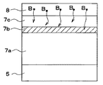
このゲート絶縁膜7は、トレンチ6の側壁部に形成されたいわゆるONO膜7fと、トレンチ6の上部、底部に形成されたシリコン酸化膜7d、7eとからなる。
【0020】
さらにONO膜7fは、トレンチ6側の第1のシリコン酸化膜7aと、シリコン窒化膜7bと、ゲート電極8側の第2のシリコン酸化膜7cとから構成されている。なお、以下では、トレンチ6側の第1のシリコン酸化膜7aをボトム酸化膜、ゲート電極8側の第2のシリコン酸化膜7cをトップ酸化膜と呼ぶ。
【0021】
シリコン窒化膜7bはボロンがこの膜を通過するのを防ぐことができる膜厚および膜質となっている。具体的には、膜厚は例えば10〜30nmとなっている。また、シリコン窒化膜7bはその上端がN型層3とP+型層4の境界より上、すなわち半導体基板5の一面側に位置している。
【0022】
ボトム酸化膜7aの膜厚は例えば100nm程度であり、トップ酸化膜7cの膜厚は例えば10〜30nmである。このようにボトム酸化膜7aの膜厚はトップ酸化膜7cの膜厚よりも大きくなっている。
【0023】
一方、トレンチ6の上部、底部に形成されたシリコン酸化膜7d、7eは、トレンチ6の側壁部に形成されたONO膜7fよりも膜厚が大きい膜となっている。ここで、トレンチ6の上部は、トレンチ6の上側のコーナー部を含む部分であり、トレンチ6の底部は、トレンチ6の底側のコーナー部を含む部分である。
【0024】
ゲート電極8は、ボロンがドープされたポリシリコンにより構成されている。
また、ベース領域となるN型層3およびソース領域となるP+型層4の一面、つまり半導体基板5の表面上にはBPSG膜9が形成されており、このBPSG膜9に形成されたコンタクトホールを介し、ソース電極10および図1には図示されないゲート、コレクタ電極となる金属膜が形成されている。
【0025】
半導体装置を上記した構成とすることにより、トレンチ6の内壁上に形成されたONO膜7f等をゲート絶縁膜7とし、N型層3におけるトレンチ6の側壁近辺の領域をチャネル領域3aとする、トレンチゲート構造を持つトランジスタが構成される。
【0026】
ここで、ゲート絶縁膜7において、トレンチ6の側壁部にはボトム酸化膜7aとシリコン窒化膜7bとトップ酸化膜7cとからなるONO膜7fが形成されている。このため、トレンチ6の側壁部におけるゲート絶縁膜がシリコン酸化膜のみから構成された場合と比較して、高いゲート耐圧が得られている。また、トレンチ6の上部、底部には、トレンチ6の側壁部に形成された積層膜よりも膜厚が大きなシリコン酸化膜7d、7eが形成されている。このため、トレンチ6の上下のコーナー部での電界集中が緩和され、その部分での電解集中による耐圧の低下が防止されている。
【0027】
次に、上記した半導体装置の製造方法について、図2に示す工程図を参照して説明する。
【0028】
まず、図2(a)に示す工程において、P+型あるいはN+型のシリコン基板1の上にP−型のドリフト層2を形成し、ついで、ベース領域となるN型層3、およびソース領域となるP+型層4をイオン注入および不純物を拡散させるための熱処理によって順次形成する。このとき、N型層3の深さを2〜3μm、P+型層4の深さを約0.5μmとする。
【0029】
次に、図2(b)に示す工程において、トレンチマスクとなるシリコン酸化膜11をCVD法により0.5μm程度堆積し、フォトリソグラフィーおよび異方性ドライエッチングによってパターニングを行う。次いで、パターニングされたシリコン酸化膜11をマスクとして、異方性ドライエッチングにより、P+型層4およびN型層3を貫通し、ドリフト層2に達するトレンチ6を形成する。このとき、トレンチ6の深さを2〜6μmとする。
【0030】
次に、図2(c)に示す工程において、CF4およびO2ガスを用いたケミカルドライエッチングによりトレンチ6を構成する内壁の表面を0.1μm程度等方的にエッチング除去する。そして、H2OまたはO2雰囲気中の熱酸化により、l00nm程度の犠牲酸化膜を形成する。この後、希フッ酸によるウェットエッチングにて、犠牲酸化膜を除去する。このとき、トレンチマスク用の酸化膜11も同時にエッチングされる。ウェットエッチングの時間は、犠牲酸化膜のみを除去する時間、犠牲酸化膜とトレンチマスク用のシリコン酸化膜11の両方を除去する時間のどちらに設定してもよい。
【0031】
続いて、後に形成するトップ酸化膜7c(図1参照)よりも膜厚が大きくなるように、トレンチ6の内壁上にボトム酸化膜としての第1のシリコン酸化膜7aを形成する。具体的には、H2OまたはO2雰囲気中の熱酸化により、100nm程度の膜厚となるように、シリコン酸化膜7aを形成する。
【0032】
次に、図2(d)に示す工程において、後に形成するゲート電極8に含まれるボロンがボトム酸化膜7aに拡散するのを防ぐことができるように、ボロンが通過するのを抑制できる膜厚および膜質にてシリコン窒化膜7bを形成する。具体的には、LPCVD法により、膜厚が10〜30nmのシリコン窒化膜7bを形成する。
【0033】
なお、シリコン窒化膜7bをN2雰囲気中の熱酸化により形成することもできる。CVD法によりシリコン窒化膜7bを形成する方法とN2雰囲気中の熱酸化によりシリコン窒化膜7bを形成する方法とでは、同じ膜厚のシリコン窒化膜7bを形成したとき、前者の方が後者よりも容易に膜厚が厚いシリコン窒化膜7bを形成できる。このことから、前者の方法によりシリコン窒化膜7bを形成することが好ましい。
【0034】
次に、図2(e)に示す工程において、CHF3およびO2ガス系を用いた異方性ドライエッチングにより、シリコン窒化膜7bのうち、トレンチ6の側壁部のシリコン窒化膜を残し、トレンチ6の底部のシリコン窒化膜を除去して、第1のシリコン酸化膜7aを露出させる。このとき、同時にトレンチ6の上部および基板表面のシリコン酸化膜11上に形成されたシリコン窒化膜も同時に除去され、その部分において第1のシリコン酸化膜7aが露出する。
【0035】
次に、図2(f)に示す工程において、第1のシリコン酸化膜7aよりも膜厚が小さくなるように、シリコン窒化膜7bの上にトップ酸化膜としての第2のシリコン酸化膜7cを形成する。具体的には、例えば、950℃のH2OもしくはO2雰囲気中で熱酸化を行い、5〜10nmの第2のシリコン酸化膜7cを形成する。
【0036】
このようにして、トレンチ6の側壁部では、ボトム酸化膜7a、シリコン窒化膜7b、トップ酸化膜7cから構成されたONO膜7fが形成される。また、シリコン窒化膜が除去されたトレンチ6の上部、底部には、熱酸化によって膜厚が大きくなった約200nmのシリコン酸化膜7d、7eが形成される。これにより、トレンチ6の上部と底部におけるコーナー部での電界集中を緩和することができるため、その部分でのゲート絶縁膜7の電界集中による耐圧の低下を防ぐことができる。
【0037】
次に、図2(g)に示す工程において、トレンチ6の内部を含む半導体基板5の表面上にボロンがドープされたポリシリコン8をLPCVD法により形成し、トレンチ6の内部を充填する。続いて、そのポリシリコン8を所望の厚さにエッチバックする。
【0038】
次に、図2(h)の工程において、フォトリソグラフィーによって多結晶シリコン8をパターニングし、ゲート電極8を形成する。
【0039】
この後、図1に示すように、層間絶縁膜となるBPSG膜9をプラズマCVD法により成膜し、さらにBPSG膜9の表面を平坦化するための熱処理を行う。そして、フォトリソグラフィーおよび異方性ドライエッチによりコンタクトホールを形成し、ソース、ゲートおよびコレクタ電極となる金属膜をスパッタ法により形成する。このようにして、図1に示す半導体装置が製造される。
【0040】
以下に本実施形態の特徴を説明する。ボロンが注入されたP+型ポリシリコンをゲート電極として用いた場合、例えば図2(h)のゲート電極8を形成する工程の後に行うBPSG膜9を平坦化するための熱処理により、ゲート電極8に含まれるボロンがトップ酸化膜7cおよびシリコン窒化膜7b中に拡散する。そして、従来では、シリコン窒化膜7bの膜厚や膜質によっては、ボロンがシリコン窒化膜7bを通過し、さらにボトム酸化膜7a中やチャネル領域3a中にもボロンが拡散する恐れがあった。
【0041】
このことから、従来ではゲート絶縁膜7の膜質が劣化するためゲート絶縁膜7の耐圧が設定値よりも低下したり、チャネル領域3aの不純物濃度が変動することで、しきい値電圧が設定値から変動するという問題が発生する恐れがあった。
【0042】
これに対して、本実施形態では、トレンチ6の側壁部に形成したONO膜7fにおいて、シリコン窒化膜7bをボロンが通過するのを防ぐことができる膜厚および膜質にて形成している。
【0043】
これにより、ゲート電極8の形成後のBPSG膜9に対する熱処理によるゲート電極8に含まれるボロンの拡散をシリコン窒化膜7bにて食い止めることができる。このため、ボトム酸化膜7aおよびチャネル領域3aにボロンが拡散するのを防ぐことができる。したがって、ゲート絶縁膜の耐圧の低下やチャネル領域3aの不純物濃度の変動を抑制することができ、ゲート絶縁膜7の耐圧やしきい値電圧が設定値から変動するのを抑制することができる。
【0044】
図3に図1中の一点鎖線にて示す領域21の拡大図を示す。図3は領域21を90°回転させた図であり、上からゲート電極8、ONO膜7fおよび半導体基板5を示している。また、図4に図3とは反対にONO膜7f中のトップ酸化膜7cをボトム酸化膜7aよりも厚くしたときの図を示す。
【0045】
本実施形態では、図3に示すように、ONO膜7fのシリコン酸化膜をトップ酸化膜7cは薄く、ボトム酸化膜7aは厚くなるように形成している。これにより、図4に示すように、トップ酸化膜7cをボトム酸化膜7aよりも厚く形成するときよりも、ONO膜7f全体に対してボロンが拡散する領域を少なくすることができる。すなわち、ONO膜7f全体に対するボロンの拡散を効果的に抑制することができる。
【0046】
このことから、本実施形態のように、ONO膜7fにおいて、ボトム酸化膜7aの膜厚をトップ酸化膜7cの膜厚よりも大きくなるようにすることで、これとは反対にトップ酸化膜7cの膜厚をボトム酸化膜7aの膜厚よりも大きくする場合と比較して、ゲート電極8の形成後の熱処理によるボロンの拡散により、膜質が劣化する領域を少なくすることができる。これにより、ゲート絶縁膜7の側壁部での耐圧が設定値よりも低下するのを抑制することができる。
【0047】
なお、本実施形態では上述したようにONO膜7fにおいて、ボロンの拡散により汚染される領域を少なくしている。したがって、ボロンの拡散が抑制されているボトム酸化膜7aの耐圧が、ONO膜7f全体の目標耐圧となるように、ボトム酸化膜7aの膜厚等を設計するのが良い。
【0048】
これまでに説明してきたように、本実施形態によれば、ゲート絶縁膜7として、トレンチ6の上部、底部には膜厚が大きなシリコン酸化膜7d、7eを形成することにより、トレンチ6の上部、底部におけるゲート絶縁膜7の耐圧を向上させることができ、さらに、トレンチ6の側壁部におけるONO膜7fを上述したように形成することにより、トレンチ6の側壁部におけるゲート絶縁膜7の耐圧も向上させることができる。
(第2実施形態)
第1実施形態では、トレンチゲート型の半導体装置の製造方法において、ベース領域としてのN型層3やソース領域としてのP+型層4をゲート電極8よりも先に形成する場合を説明したが、ゲート電極8を形成した後に、N型層3やP+型層4をイオン注入及び不純物拡散のための熱処理により形成することもできる。
【0049】
この場合では、図2(a)〜(h)に示す工程のうち、図2(a)に示す工程ではN型層3やP+型層4の形成を行わず、図2(h)に示す工程にて、ゲート電極を形成した後、ドリフト層2のうちN型層3やP+型層4を形成する領域の表面上のシリコン酸化膜11を除去する。そして、N型層3やP+型層4をイオン注入及び不純物拡散のための熱処理により形成するように製造工程を変更する。なお、その他のゲート絶縁膜7を形成する等の図2(b)〜図2(f)に示す工程は第1実施形態と同様に行う。
【0050】
N型層3やP+型層4を形成した後、図1に示すように、層間絶縁膜となるBPSG膜9をプラズマCVD法により成膜し、さらにBPSG膜9の表面を平坦化するための熱処理を行う。その後も第1実施形態と同様に行うことで、半導体装置を製造することができる。
【0051】
この場合においては、N型層3やP+型層4を形成する際の不純物を拡散させるための熱処理や、第1実施形態と同様にBPSG膜9の平坦化のための熱処理により、ゲート電極8に含まれるボロンがゲート絶縁膜および半導体基板5に向かって拡散する恐れがある。
【0052】
したがって、本実施形態においても、ゲート絶縁膜7を構成するONO膜7fを第1実施形態と同様に形成することで、ゲート電極の形成後における不純物拡散のための熱処理や、BPSG膜9の平坦化のための熱処理等により、ゲート電極8からゲート絶縁膜7に対するボロンの拡散を効果的に抑制することができる。
(他の実施形態)
なお、上記した各実施形態では、トレンチ6の上部および底部の絶縁膜をシリコン酸化膜のみにより形成する場合を説明したが、トレンチの上部および底部のいずれか一方のみをシリコン酸化膜により構成し、他方をONO膜により構成することもできる。トレンチの上部および底部のいずれか一方のみをシリコン酸化膜にするためには、他方のシリコン窒化膜を除去しないようにマスクして異方性ドライエッチングを行うように上記した製造工程を変更すればよい。
【0053】
また、ゲート絶縁膜7を全てONO膜により構成することもできる。この場合は、上記した製造工程において、シリコン窒化膜7bを除去せず、その上にシリコン酸化膜7cを形成するように製造工程を変更すれば良い。
【0054】
また、上記した各実施形態では、Pチャネル型のトランジスタを有する半導体装置を例として説明したが、ボロンがドープされたポリシリコンをゲート電極として用いており、かつ、半導体装置の各層の導電型をそれぞれ反対の導電型としたNチャネル型のトランジスタを有する半導体装置においても、本発明を適用することができる。
【0055】
また、上記した各実施形態では、半導体装置として、パワーMOSFET、IGBT等のトランジスタを構成するものを例として説明したが、これに限らず、トレンチの内部にポリシリコンが埋め込まれたトレンチ型のキャパシタを備える半導体装置等のトレンチゲート構造を有する半導体装置においても本発明を適用することができる。
【0056】
この場合においても、トレンチの内壁上に形成する絶縁膜をONO膜により構成し、ONO膜を構成するシリコン窒化膜をボロンの通過を抑制できる膜厚および膜質にて形成し、トップ酸化膜は薄く、ボトム酸化膜は厚くなるように、それぞれのシリコン酸化膜を形成する。
【0057】
このようにシリコン窒化膜を形成することで、ゲート電極の形成後の熱処理によるゲート電極に含まれるボロンの拡散をシリコン窒化膜にて食い止めることができ、ボトム酸化膜にボロンが拡散するのを防ぐことができる。
【0058】
さらに、ボトム酸化膜をトップ酸化膜よりも厚く形成することで、ONO膜中におけるボロンが拡散する領域を少なくすることができる。これにより、ボロンの拡散を効果的に抑制することができるため、トレンチの内壁上に形成された絶縁膜の耐圧が、設定値よりも低下するのを抑制することができる。
【図面の簡単な説明】
【図1】本発明の第1実施形態における半導体装置の断面図である。
【図2】図1に示す半導体装置の製造工程を示す図である。
【図3】図1中の領域21の拡大図である。
【図4】図3よりもゲート絶縁膜7の耐圧が低いときの例を示す図である。
【符号の説明】
1…シリコン基板、2…ドリフト層、3…N型層、3a…チャネル領域、
4…P+型層、5…半導体基板、6…トレンチ、7…ゲート絶縁膜、
7a…シリコン酸化膜(ボトム酸化膜)、7b…シリコン窒化膜、
7c…シリコン酸化膜(トップ酸化膜)、7d、7e…シリコン酸化膜、
7f…ONO膜、8…ゲート電極、9…BPSG膜、10…ソース電極、
11…シリコン酸化膜。[0001]
TECHNICAL FIELD OF THE INVENTION
The present invention relates to a semiconductor device having a trench gate structure and a method for manufacturing the same.
[0002]
[Prior art]
Conventionally, there is a semiconductor device having a so-called trench gate structure in which a gate insulating film is formed on a side wall of a trench formed on one surface of a semiconductor substrate, and a gate electrode is buried in the trench.
[0003]
In such a semiconductor device, there is a semiconductor device in which a gate insulating film is formed of a stacked film of a silicon oxide film, a silicon nitride film, and a silicon oxide film, that is, a so-called ONO (Oxide Nitride Oxide) film. In this semiconductor device, since the gate insulating film is formed of the ONO film, the gate withstand voltage is higher than when the gate insulating film is formed only of the silicon oxide film. (For example, see Patent Document 1)
In the process of manufacturing a semiconductor device having such a trench gate structure, a gate electrode is generally formed of polysilicon doped with impurities such as B (boron) and P (phosphorus). After the formation of the gate electrode, an interlayer insulating film is formed on the gate electrode, and heat treatment is performed to planarize the interlayer insulating film. In the case where an impurity diffusion layer such as a source region is formed after forming a gate electrode, ion implantation is performed after the gate electrode is formed to form a source region or the like, and heat treatment for diffusing impurities is performed. Is
[0004]
[Patent Document 1]
JP 2001-196587 A
[Problems to be solved by the invention]
In the above-described manufacturing process, particularly, when P + -type polysilicon doped with boron is used as the gate electrode, when heat treatment is performed after the formation of the gate electrode, boron contained in the gate electrode is contained in the gate insulating film. May spread. As a result, the quality of the gate insulating film is degraded, and there is a possibility that a problem that the withstand voltage of the gate insulating film becomes lower than a set value may occur.
[0006]
The present invention has been made in view of the above circumstances, and in a semiconductor device having a trench gate structure in which boron-doped polysilicon is embedded in a trench, it is possible to suppress a decrease in withstand voltage of an insulating film formed on a sidewall of the trench. It is an object of the present invention to provide a semiconductor device and a method for manufacturing the same.
[0007]
[Means for Solving the Problems]
In order to achieve the above object, according to the first aspect of the present invention, a laminated film (7f) is formed on the side wall of the trench, and boron-doped polysilicon (8) is embedded in the trench (6). The silicon nitride film (7b) in the laminated film (7f) has a film thickness and film quality capable of suppressing the passage of boron, and has a trench (6f) in the laminated film (7f). The thickness of the first silicon oxide film (7a) on the ()) side is larger than the thickness of the second silicon oxide film (7c) on the polysilicon (8) side.
[0008]
Among the stacked films formed on the sidewalls of the trench in this manner, the silicon nitride film is included in the polysilicon because it is formed with a film thickness and film quality that can suppress the passage of boron through this film. It is possible to suppress boron from diffusing into the first silicon oxide film on the trench side.
[0009]
Since the first silicon oxide film on the trench side is thicker than the second silicon oxide film on the polysilicon side, on the contrary, the second silicon oxide film is the first silicon oxide film on the trench side. Compared with the case where the thickness is larger than the silicon oxide film, the ratio of the region which is not contaminated with boron to the entire stacked film can be increased. Therefore, according to the present invention, it is possible to suppress a decrease in the breakdown voltage of the stacked film due to the diffusion of boron as compared with the case where the second silicon oxide film is thicker than the first silicon oxide film. .
[0010]
The invention of
[0011]
According to a second aspect of the present invention, there is provided a method of manufacturing a semiconductor device having a trench gate structure in which boron-doped polysilicon (8) is embedded in a trench (6). Forming a first silicon oxide film (7a) on the side wall so as to be thicker than a second silicon oxide film (7c) on the polysilicon (8) side; A step of forming a silicon nitride film (7b) on the film (7a) with a film thickness and film quality capable of suppressing the passage of boron, and a first step on the trench (6) side on the silicon nitride film (7b). Forming a stacked film (7f) by forming a second silicon oxide film (7c) so that the film thickness is smaller than that of the silicon oxide film (7a).
[0012]
According to this manufacturing method, the semiconductor device according to the first aspect can be manufactured.
[0013]
Further, according to the present invention, in the step of forming the silicon oxide film on the trench side, the withstand voltage design of the entire stacked film is performed by the silicon oxide film on the trench side, so that the stacked film having the target withstand voltage is formed. can do.
[0014]
The invention according to
[0015]
In addition, the code | symbol in the parenthesis of each said means shows the correspondence with the concrete means described in embodiment mentioned later.
[0016]
BEST MODE FOR CARRYING OUT THE INVENTION
(1st Embodiment)
FIG. 1 shows a cross-sectional configuration of a semiconductor device according to one embodiment of the present invention. This semiconductor device has a transistor having a trench gate structure such as a power MOSFET and an IGBT. In this embodiment, a P-channel transistor will be described as an example.
[0017]
In FIG. 1, a P − -
[0018]
On one surface of the
[0019]
The
[0020]
Further, the ONO film 7f includes a first
[0021]
The
[0022]
The thickness of the
[0023]
On the other hand, the
[0024]
The
A
[0025]
With the above-described configuration of the semiconductor device, the ONO film 7f and the like formed on the inner wall of the
[0026]
Here, in the
[0027]
Next, a method for manufacturing the above-described semiconductor device will be described with reference to the process chart shown in FIG.
[0028]
First, in a step shown in FIG. 2A, a P − -
[0029]
Next, in the step shown in FIG. 2B, a
[0030]
Next, in the step shown in FIG. 2C, the surface of the inner wall constituting the
[0031]
Subsequently, a first
[0032]
Next, in the step shown in FIG. 2D, a film thickness capable of suppressing the passage of boron so that boron contained in the
[0033]
It is also possible to form the
[0034]
Next, in the step shown in FIG. 2E, the silicon nitride film on the side wall of the
[0035]
Next, in a step shown in FIG. 2F, a second
[0036]
Thus, an ONO film 7f composed of the
[0037]
Next, in the step shown in FIG. 2G, boron-doped
[0038]
Next, in the step of FIG. 2H, the
[0039]
Thereafter, as shown in FIG. 1, a
[0040]
Hereinafter, features of the present embodiment will be described. In the case where P + -type polysilicon into which boron is implanted is used as the gate electrode, for example, a heat treatment for planarizing the
[0041]
From this, conventionally, the film quality of the
[0042]
On the other hand, in the present embodiment, the ONO film 7f formed on the side wall of the
[0043]
Thereby, the diffusion of boron contained in the
[0044]
FIG. 3 is an enlarged view of a
[0045]
In this embodiment, as shown in FIG. 3, the silicon oxide film of the ONO film 7f is formed such that the
[0046]
From this, as in the present embodiment, by making the thickness of the
[0047]
In the present embodiment, as described above, the area of the ONO film 7f that is contaminated by the diffusion of boron is reduced. Therefore, it is preferable to design the thickness and the like of the
[0048]
As described above, according to the present embodiment, the
(2nd Embodiment)
In the first embodiment, the case where the N-
[0049]
In this case, among the steps shown in FIGS. 2A to 2H, in the step shown in FIG. 2A, the N-
[0050]
After forming the N-
[0051]
In this case, a heat treatment for diffusing impurities when forming the N-
[0052]
Therefore, also in this embodiment, by forming the ONO film 7f constituting the
(Other embodiments)
In each of the above-described embodiments, the case where the insulating films at the top and bottom of the
[0053]
Further, the
[0054]
In each of the above embodiments, the semiconductor device having a P-channel transistor has been described as an example. However, boron-doped polysilicon is used as the gate electrode, and the conductivity type of each layer of the semiconductor device is changed. The present invention can be applied to a semiconductor device having N-channel transistors of opposite conductivity types.
[0055]
Further, in each of the above-described embodiments, a semiconductor device that constitutes a transistor such as a power MOSFET or an IGBT has been described as an example. However, the present invention is not limited to this, and a trench-type capacitor in which polysilicon is embedded in a trench is used. The present invention can also be applied to a semiconductor device having a trench gate structure, such as a semiconductor device including a semiconductor device.
[0056]
Also in this case, the insulating film formed on the inner wall of the trench is formed of an ONO film, the silicon nitride film forming the ONO film is formed with a film thickness and film quality capable of suppressing the passage of boron, and the top oxide film is formed thin. Then, each silicon oxide film is formed so that the bottom oxide film becomes thick.
[0057]
By forming the silicon nitride film in this manner, the diffusion of boron contained in the gate electrode due to the heat treatment after the formation of the gate electrode can be prevented by the silicon nitride film, and the diffusion of boron into the bottom oxide film is prevented. be able to.
[0058]
Further, by forming the bottom oxide film thicker than the top oxide film, the region where boron is diffused in the ONO film can be reduced. Thus, the diffusion of boron can be effectively suppressed, so that the breakdown voltage of the insulating film formed on the inner wall of the trench can be suppressed from lowering below a set value.
[Brief description of the drawings]
FIG. 1 is a sectional view of a semiconductor device according to a first embodiment of the present invention.
FIG. 2 is a view illustrating a manufacturing process of the semiconductor device illustrated in FIG. 1;
FIG. 3 is an enlarged view of a
FIG. 4 is a diagram showing an example when the withstand voltage of the
[Explanation of symbols]
DESCRIPTION OF
4 ... P + type layer, 5 ... semiconductor substrate, 6 ... trench, 7 ... gate insulating film,
7a: silicon oxide film (bottom oxide film); 7b: silicon nitride film;
7c: silicon oxide film (top oxide film), 7d, 7e: silicon oxide film,
7f ONO film, 8 gate electrode, 9 BPSG film, 10 source electrode,
11: silicon oxide film.
Claims (2)
前記積層膜(7f)中の前記シリコン窒化膜(7b)は、前記ボロンの通過を抑制できる膜厚および膜質であり、前記積層膜(7f)中の前記トレンチ(6)側の第1の前記シリコン酸化膜(7a)の膜厚は、前記ポリシリコン(8)側の第2のシリコン酸化膜(7c)の膜厚よりも大きいことを特徴とする半導体装置。A first silicon oxide film (7a), a silicon nitride film (7b), and a second silicon oxide film (7c) are sequentially stacked on side walls of a trench (6) formed on one surface of a semiconductor substrate (5). A semiconductor device having a trench gate structure in which a laminated film (7f) is formed, and boron-doped polysilicon (8) is embedded in the trench (6) through the laminated film,
The silicon nitride film (7b) in the laminated film (7f) has a thickness and a film quality capable of suppressing the passage of the boron, and the first nitride film (7b) in the laminated film (7f) on the trench (6) side has the first structure. A semiconductor device, wherein the thickness of the silicon oxide film (7a) is larger than the thickness of the second silicon oxide film (7c) on the polysilicon (8) side.
前記半導体基板(5)の一面に前記トレンチ(6)を形成する工程と、
前記トレンチ(6)の側壁上に、前記ポリシリコン(8)側の前記第2のシリコン酸化膜(7c)よりも膜厚が大きくなるように、前記第1のシリコン酸化膜(7a)を形成する工程と、
前記第1の前記シリコン酸化膜(7a)の上に、前記ボロンが通過を抑制できる膜厚および膜質にて前記シリコン窒化膜(7b)を形成する工程と、
前記シリコン窒化膜(7b)の上に、前記トレンチ(6)側の第1のシリコン酸化膜(7a)よりも膜厚が小さくなるように、前記第2のシリコン酸化膜(7c)を形成することで前記積層膜(7f)を形成する工程とを有することを特徴とする半導体装置の製造方法。A lamination in which a first silicon oxide film (7a), a silicon nitride film (7b), and a second silicon oxide film (7c) are laminated on a side wall of a trench (6) formed on one surface of a semiconductor substrate (5). Manufacturing of a semiconductor device having a trench gate structure in which a film (7f) is formed and boron-doped polysilicon (8) is embedded in the trench (6) via the laminated film (7f). The method,
Forming the trench (6) on one surface of the semiconductor substrate (5);
The first silicon oxide film (7a) is formed on the side wall of the trench (6) so as to be thicker than the second silicon oxide film (7c) on the polysilicon (8) side. The process of
Forming the silicon nitride film (7b) on the first silicon oxide film (7a) with a film thickness and film quality capable of suppressing the passage of the boron;
The second silicon oxide film (7c) is formed on the silicon nitride film (7b) so as to be thinner than the first silicon oxide film (7a) on the trench (6) side. Forming the laminated film (7f).
Priority Applications (2)
| Application Number | Priority Date | Filing Date | Title |
|---|---|---|---|
| JP2003014466A JP2004228342A (en) | 2003-01-23 | 2003-01-23 | Semiconductor device and its manufacturing method |
| US10/726,590 US6974996B2 (en) | 2003-01-23 | 2003-12-04 | Semiconductor device and method of manufacturing the same |
Applications Claiming Priority (1)
| Application Number | Priority Date | Filing Date | Title |
|---|---|---|---|
| JP2003014466A JP2004228342A (en) | 2003-01-23 | 2003-01-23 | Semiconductor device and its manufacturing method |
Publications (1)
| Publication Number | Publication Date |
|---|---|
| JP2004228342A true JP2004228342A (en) | 2004-08-12 |
Family
ID=32732792
Family Applications (1)
| Application Number | Title | Priority Date | Filing Date |
|---|---|---|---|
| JP2003014466A Pending JP2004228342A (en) | 2003-01-23 | 2003-01-23 | Semiconductor device and its manufacturing method |
Country Status (2)
| Country | Link |
|---|---|
| US (1) | US6974996B2 (en) |
| JP (1) | JP2004228342A (en) |
Cited By (1)
| Publication number | Priority date | Publication date | Assignee | Title |
|---|---|---|---|---|
| KR100683089B1 (en) | 2005-08-24 | 2007-02-15 | 삼성전자주식회사 | Recessed gate structure, method of forming the recessed gate structure, semiconductor device having the recessed gate structure and method of manufacturing the semiconductor device |
Families Citing this family (6)
| Publication number | Priority date | Publication date | Assignee | Title |
|---|---|---|---|---|
| JP2006216897A (en) * | 2005-02-07 | 2006-08-17 | Toshiba Corp | Semiconductor device and manufacturing method therefor |
| US8497549B2 (en) * | 2007-08-21 | 2013-07-30 | Fairchild Semiconductor Corporation | Method and structure for shielded gate trench FET |
| JP5587535B2 (en) * | 2007-11-14 | 2014-09-10 | ローム株式会社 | Semiconductor device |
| US20100013009A1 (en) * | 2007-12-14 | 2010-01-21 | James Pan | Structure and Method for Forming Trench Gate Transistors with Low Gate Resistance |
| JP5452195B2 (en) | 2009-12-03 | 2014-03-26 | 株式会社 日立パワーデバイス | Semiconductor device and power conversion device using the same |
| CN102097378B (en) * | 2009-12-10 | 2013-12-04 | 力士科技股份有限公司 | Method for manufacturing trench metal-oxide semiconductor field effect transistor (MOSFET) |
Family Cites Families (10)
| Publication number | Priority date | Publication date | Assignee | Title |
|---|---|---|---|---|
| US4785337A (en) * | 1986-10-17 | 1988-11-15 | International Business Machines Corporation | Dynamic ram cell having shared trench storage capacitor with sidewall-defined bridge contacts and gate electrodes |
| US4833094A (en) * | 1986-10-17 | 1989-05-23 | International Business Machines Corporation | Method of making a dynamic ram cell having shared trench storage capacitor with sidewall-defined bridge contacts and gate electrodes |
| JP3167457B2 (en) * | 1992-10-22 | 2001-05-21 | 株式会社東芝 | Semiconductor device |
| JP2871530B2 (en) * | 1995-05-10 | 1999-03-17 | 日本電気株式会社 | Method for manufacturing semiconductor device |
| JP2000196074A (en) | 1998-12-25 | 2000-07-14 | Toshiba Corp | Semiconductor device and its manufacture |
| ITMI20010039A1 (en) * | 2000-01-14 | 2002-07-11 | Denso Corp | SEMICONDUCTOR DEVICE AND METHOD FOR MANUFACTURING ITSELF |
| US6864532B2 (en) * | 2000-01-14 | 2005-03-08 | Denso Corporation | Semiconductor device and method for manufacturing the same |
| JP2001326273A (en) * | 2000-05-16 | 2001-11-22 | Denso Corp | Method for manufacturing semiconductor device |
| JP2003060207A (en) * | 2001-08-09 | 2003-02-28 | Mitsubishi Electric Corp | Semiconductor device and manufacturing method therefor |
| JP2003224274A (en) | 2002-01-28 | 2003-08-08 | Denso Corp | Semiconductor device |
-
2003
- 2003-01-23 JP JP2003014466A patent/JP2004228342A/en active Pending
- 2003-12-04 US US10/726,590 patent/US6974996B2/en not_active Expired - Lifetime
Cited By (1)
| Publication number | Priority date | Publication date | Assignee | Title |
|---|---|---|---|---|
| KR100683089B1 (en) | 2005-08-24 | 2007-02-15 | 삼성전자주식회사 | Recessed gate structure, method of forming the recessed gate structure, semiconductor device having the recessed gate structure and method of manufacturing the semiconductor device |
Also Published As
| Publication number | Publication date |
|---|---|
| US6974996B2 (en) | 2005-12-13 |
| US20040145012A1 (en) | 2004-07-29 |
Similar Documents
| Publication | Publication Date | Title |
|---|---|---|
| US7354829B2 (en) | Trench-gate transistor with ono gate dielectric and fabrication process therefor | |
| US6469345B2 (en) | Semiconductor device and method for manufacturing the same | |
| JP2005209807A (en) | Insulated gate semiconductor device and its manufacturing method | |
| JP2008166696A (en) | Transistor having recess channel, and its manufacturing method | |
| JP2004266140A (en) | Semiconductor device and its manufacturing method | |
| JP5198760B2 (en) | Semiconductor device and manufacturing method thereof | |
| JP2009302450A (en) | Semiconductor device and its manufacturing method | |
| JP4618766B2 (en) | Semiconductor device | |
| JP2005150522A (en) | Semiconductor device and manufacturing method thereof | |
| JP2004228342A (en) | Semiconductor device and its manufacturing method | |
| US6744113B2 (en) | Semiconductor device with element isolation using impurity-doped insulator and oxynitride film | |
| JP4192381B2 (en) | Semiconductor device and manufacturing method thereof | |
| JP2001196587A (en) | Semiconductor device and method of manufacturing the same | |
| KR20120053511A (en) | Method for fabricating trench dmos transistor | |
| US7723784B2 (en) | Insulated gate semiconductor device and method for manufacturing the same | |
| JP4223026B2 (en) | Semiconductor device | |
| JP2006093506A (en) | Insulation gate type semiconductor device and its manufacturing method | |
| JP5738094B2 (en) | Manufacturing method of semiconductor device | |
| JP2008004686A (en) | Method of manufacturing semiconductor device | |
| JP4826036B2 (en) | Manufacturing method of semiconductor device | |
| JP2000223708A (en) | Semiconductor device | |
| JP4984697B2 (en) | Manufacturing method of semiconductor device | |
| KR100234692B1 (en) | Transistor and the manufacturing method thereof | |
| JP3608999B2 (en) | Manufacturing method of semiconductor device | |
| JP4067783B2 (en) | Manufacturing method of semiconductor device |
Legal Events
| Date | Code | Title | Description |
|---|---|---|---|
| A621 | Written request for application examination |
Free format text: JAPANESE INTERMEDIATE CODE: A621 Effective date: 20050323 |
|
| A977 | Report on retrieval |
Free format text: JAPANESE INTERMEDIATE CODE: A971007 Effective date: 20070830 |
|
| A131 | Notification of reasons for refusal |
Free format text: JAPANESE INTERMEDIATE CODE: A131 Effective date: 20070904 |
|
| A02 | Decision of refusal |
Free format text: JAPANESE INTERMEDIATE CODE: A02 Effective date: 20080108 |