JP2004203049A - インクジェットプリントヘッド及びその製造方法 - Google Patents
インクジェットプリントヘッド及びその製造方法 Download PDFInfo
- Publication number
- JP2004203049A JP2004203049A JP2003425225A JP2003425225A JP2004203049A JP 2004203049 A JP2004203049 A JP 2004203049A JP 2003425225 A JP2003425225 A JP 2003425225A JP 2003425225 A JP2003425225 A JP 2003425225A JP 2004203049 A JP2004203049 A JP 2004203049A
- Authority
- JP
- Japan
- Prior art keywords
- conductor
- ink
- forming
- insulating layer
- print head
- Prior art date
- Legal status (The legal status is an assumption and is not a legal conclusion. Google has not performed a legal analysis and makes no representation as to the accuracy of the status listed.)
- Granted
Links
- 238000004519 manufacturing process Methods 0.000 title abstract description 37
- 239000004020 conductor Substances 0.000 claims abstract description 150
- 238000005192 partition Methods 0.000 claims abstract description 33
- 239000010410 layer Substances 0.000 claims description 101
- 239000000758 substrate Substances 0.000 claims description 48
- 238000000034 method Methods 0.000 claims description 45
- 239000011241 protective layer Substances 0.000 claims description 25
- 239000000463 material Substances 0.000 claims description 16
- 238000000151 deposition Methods 0.000 claims description 13
- 238000000059 patterning Methods 0.000 claims description 11
- 239000007769 metal material Substances 0.000 claims description 10
- ATJFFYVFTNAWJD-UHFFFAOYSA-N Tin Chemical compound [Sn] ATJFFYVFTNAWJD-UHFFFAOYSA-N 0.000 claims description 8
- 238000007599 discharging Methods 0.000 claims description 6
- 238000001312 dry etching Methods 0.000 claims description 6
- 230000008878 coupling Effects 0.000 claims description 2
- 238000010168 coupling process Methods 0.000 claims description 2
- 238000005859 coupling reaction Methods 0.000 claims description 2
- 238000009413 insulation Methods 0.000 abstract description 6
- 230000008569 process Effects 0.000 description 25
- 229910052751 metal Inorganic materials 0.000 description 13
- 239000002184 metal Substances 0.000 description 13
- MZLGASXMSKOWSE-UHFFFAOYSA-N tantalum nitride Chemical compound [Ta]#N MZLGASXMSKOWSE-UHFFFAOYSA-N 0.000 description 13
- 229920000642 polymer Polymers 0.000 description 11
- 239000010408 film Substances 0.000 description 9
- XUIMIQQOPSSXEZ-UHFFFAOYSA-N Silicon Chemical compound [Si] XUIMIQQOPSSXEZ-UHFFFAOYSA-N 0.000 description 7
- 229910052710 silicon Inorganic materials 0.000 description 7
- 239000010703 silicon Substances 0.000 description 7
- 229910000838 Al alloy Inorganic materials 0.000 description 6
- PXHVJJICTQNCMI-UHFFFAOYSA-N Nickel Chemical compound [Ni] PXHVJJICTQNCMI-UHFFFAOYSA-N 0.000 description 6
- 229910052782 aluminium Inorganic materials 0.000 description 6
- XAGFODPZIPBFFR-UHFFFAOYSA-N aluminium Chemical compound [Al] XAGFODPZIPBFFR-UHFFFAOYSA-N 0.000 description 6
- 230000004888 barrier function Effects 0.000 description 6
- 229910052581 Si3N4 Inorganic materials 0.000 description 5
- HQVNEWCFYHHQES-UHFFFAOYSA-N silicon nitride Chemical compound N12[Si]34N5[Si]62N3[Si]51N64 HQVNEWCFYHHQES-UHFFFAOYSA-N 0.000 description 5
- 239000010409 thin film Substances 0.000 description 5
- 239000004642 Polyimide Substances 0.000 description 4
- VYPSYNLAJGMNEJ-UHFFFAOYSA-N Silicium dioxide Chemical compound O=[Si]=O VYPSYNLAJGMNEJ-UHFFFAOYSA-N 0.000 description 4
- 238000005530 etching Methods 0.000 description 4
- 238000010438 heat treatment Methods 0.000 description 4
- 238000010030 laminating Methods 0.000 description 4
- 229920001721 polyimide Polymers 0.000 description 4
- 229910052814 silicon oxide Inorganic materials 0.000 description 4
- 230000001070 adhesive effect Effects 0.000 description 3
- 239000011248 coating agent Substances 0.000 description 3
- 238000000576 coating method Methods 0.000 description 3
- 229910052759 nickel Inorganic materials 0.000 description 3
- 238000000206 photolithography Methods 0.000 description 3
- 229920002120 photoresistant polymer Polymers 0.000 description 3
- 229910052715 tantalum Inorganic materials 0.000 description 3
- GUVRBAGPIYLISA-UHFFFAOYSA-N tantalum atom Chemical compound [Ta] GUVRBAGPIYLISA-UHFFFAOYSA-N 0.000 description 3
- 239000010419 fine particle Substances 0.000 description 2
- 238000003475 lamination Methods 0.000 description 2
- 230000007246 mechanism Effects 0.000 description 2
- 230000004048 modification Effects 0.000 description 2
- 238000012986 modification Methods 0.000 description 2
- 238000005507 spraying Methods 0.000 description 2
- 238000004544 sputter deposition Methods 0.000 description 2
- 239000000853 adhesive Substances 0.000 description 1
- RVSGESPTHDDNTH-UHFFFAOYSA-N alumane;tantalum Chemical compound [AlH3].[Ta] RVSGESPTHDDNTH-UHFFFAOYSA-N 0.000 description 1
- 238000004380 ashing Methods 0.000 description 1
- 238000009835 boiling Methods 0.000 description 1
- 238000005229 chemical vapour deposition Methods 0.000 description 1
- -1 for example Polymers 0.000 description 1
- 230000020169 heat generation Effects 0.000 description 1
- 239000011810 insulating material Substances 0.000 description 1
- 150000002739 metals Chemical class 0.000 description 1
- 238000001259 photo etching Methods 0.000 description 1
- 238000003825 pressing Methods 0.000 description 1
- 230000002265 prevention Effects 0.000 description 1
- 239000004065 semiconductor Substances 0.000 description 1
- 239000000126 substance Substances 0.000 description 1
Images


Classifications
-
- B—PERFORMING OPERATIONS; TRANSPORTING
- B41—PRINTING; LINING MACHINES; TYPEWRITERS; STAMPS
- B41J—TYPEWRITERS; SELECTIVE PRINTING MECHANISMS, i.e. MECHANISMS PRINTING OTHERWISE THAN FROM A FORME; CORRECTION OF TYPOGRAPHICAL ERRORS
- B41J2/00—Typewriters or selective printing mechanisms characterised by the printing or marking process for which they are designed
- B41J2/22—Typewriters or selective printing mechanisms characterised by the printing or marking process for which they are designed characterised by selective application of impact or pressure on a printing material or impression-transfer material
- B41J2/23—Typewriters or selective printing mechanisms characterised by the printing or marking process for which they are designed characterised by selective application of impact or pressure on a printing material or impression-transfer material using print wires
- B41J2/235—Print head assemblies
-
- B—PERFORMING OPERATIONS; TRANSPORTING
- B41—PRINTING; LINING MACHINES; TYPEWRITERS; STAMPS
- B41J—TYPEWRITERS; SELECTIVE PRINTING MECHANISMS, i.e. MECHANISMS PRINTING OTHERWISE THAN FROM A FORME; CORRECTION OF TYPOGRAPHICAL ERRORS
- B41J2/00—Typewriters or selective printing mechanisms characterised by the printing or marking process for which they are designed
- B41J2/005—Typewriters or selective printing mechanisms characterised by the printing or marking process for which they are designed characterised by bringing liquid or particles selectively into contact with a printing material
- B41J2/01—Ink jet
- B41J2/135—Nozzles
- B41J2/16—Production of nozzles
- B41J2/1621—Manufacturing processes
- B41J2/1631—Manufacturing processes photolithography
-
- B—PERFORMING OPERATIONS; TRANSPORTING
- B41—PRINTING; LINING MACHINES; TYPEWRITERS; STAMPS
- B41J—TYPEWRITERS; SELECTIVE PRINTING MECHANISMS, i.e. MECHANISMS PRINTING OTHERWISE THAN FROM A FORME; CORRECTION OF TYPOGRAPHICAL ERRORS
- B41J2/00—Typewriters or selective printing mechanisms characterised by the printing or marking process for which they are designed
- B41J2/005—Typewriters or selective printing mechanisms characterised by the printing or marking process for which they are designed characterised by bringing liquid or particles selectively into contact with a printing material
- B41J2/01—Ink jet
- B41J2/135—Nozzles
- B41J2/14—Structure thereof only for on-demand ink jet heads
- B41J2/14016—Structure of bubble jet print heads
- B41J2/14088—Structure of heating means
- B41J2/14112—Resistive element
- B41J2/14129—Layer structure
-
- B—PERFORMING OPERATIONS; TRANSPORTING
- B41—PRINTING; LINING MACHINES; TYPEWRITERS; STAMPS
- B41J—TYPEWRITERS; SELECTIVE PRINTING MECHANISMS, i.e. MECHANISMS PRINTING OTHERWISE THAN FROM A FORME; CORRECTION OF TYPOGRAPHICAL ERRORS
- B41J2/00—Typewriters or selective printing mechanisms characterised by the printing or marking process for which they are designed
- B41J2/005—Typewriters or selective printing mechanisms characterised by the printing or marking process for which they are designed characterised by bringing liquid or particles selectively into contact with a printing material
- B41J2/01—Ink jet
- B41J2/135—Nozzles
- B41J2/16—Production of nozzles
- B41J2/1601—Production of bubble jet print heads
- B41J2/1603—Production of bubble jet print heads of the front shooter type
-
- B—PERFORMING OPERATIONS; TRANSPORTING
- B41—PRINTING; LINING MACHINES; TYPEWRITERS; STAMPS
- B41J—TYPEWRITERS; SELECTIVE PRINTING MECHANISMS, i.e. MECHANISMS PRINTING OTHERWISE THAN FROM A FORME; CORRECTION OF TYPOGRAPHICAL ERRORS
- B41J2/00—Typewriters or selective printing mechanisms characterised by the printing or marking process for which they are designed
- B41J2/005—Typewriters or selective printing mechanisms characterised by the printing or marking process for which they are designed characterised by bringing liquid or particles selectively into contact with a printing material
- B41J2/01—Ink jet
- B41J2/135—Nozzles
- B41J2/16—Production of nozzles
- B41J2/1621—Manufacturing processes
- B41J2/1626—Manufacturing processes etching
- B41J2/1628—Manufacturing processes etching dry etching
-
- B—PERFORMING OPERATIONS; TRANSPORTING
- B41—PRINTING; LINING MACHINES; TYPEWRITERS; STAMPS
- B41J—TYPEWRITERS; SELECTIVE PRINTING MECHANISMS, i.e. MECHANISMS PRINTING OTHERWISE THAN FROM A FORME; CORRECTION OF TYPOGRAPHICAL ERRORS
- B41J2/00—Typewriters or selective printing mechanisms characterised by the printing or marking process for which they are designed
- B41J2/005—Typewriters or selective printing mechanisms characterised by the printing or marking process for which they are designed characterised by bringing liquid or particles selectively into contact with a printing material
- B41J2/01—Ink jet
- B41J2/135—Nozzles
- B41J2/16—Production of nozzles
- B41J2/1621—Manufacturing processes
- B41J2/164—Manufacturing processes thin film formation
- B41J2/1646—Manufacturing processes thin film formation thin film formation by sputtering
Abstract
【解決手段】 基板と,基板の表面に形成された第1絶縁層と,第1絶縁層上に上下に互いに離隔されて形成された第1及び第2導線と,第1導線と第2導線を電気的に連結する複数の導線連結部を含むヒータ部と,第1及び第2導線間に形成された第2絶縁層と,基板の上部に設けられ,インクチャンバを限定する隔壁と,隔壁の上部に設けられて前記インクチャンバの上部壁をなし,ノズルが形成されたノズルプレートとを備えるインクジェットプリントヘッドである。本発明により,別途の抵抗体を設けずとも導線間を複数の導線連結部で連結することによりヒータ部を形成できる改善された構造のインクジェットプリントヘッド及びその製造方法を実現できるようになる。
【選択図】 図2
Description
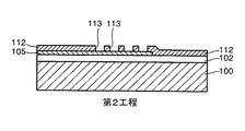
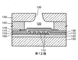
102,112 第1及び2絶縁層
104 ヒータ部
105,106 第1及び第2導線
110 導線連結部
110a 第1接面部
114 保護層
118 キャビテーション防止層
120 インクチャンバ
122 隔壁
130 ノズル
132 ノズルプレート
Claims (10)
- 基板と;
前記基板の表面に形成された第1絶縁層と;
前記第1絶縁層上に上下に互いに離隔した状態で形成される第1導線及び第2導線と;
前記第1導線と第2導線との間に,前記第1導線と第2導線を電気的に連結する1又は2以上の導線連結部を少なくとも含むヒータ部と;
前記第1導線と第2導線との間に形成され,前記1又は2以上の導線連結部を絶縁するための第2絶縁層と;
前記基板の上部に設けられ,吐出されるインクが満たされるインクチャンバを形成するための隔壁と;
前記隔壁の上部に設けられて前記インクチャンバの上部壁をなし,前記インクチャンバに満たされたインクを吐出するためのノズルが形成されたノズルプレートとを備えることを特徴とする,インクジェットプリントヘッド。 - 前記第1導線または第2導線が前記導線連結部と連結する1又は2以上の接面のうち少なくとも1つには界面が形成されることを特徴とする,請求項1に記載のインクジェットプリントヘッド。
- 前記導線連結部は前記第1導線または第2導線のうちいずれか1つから凸形状に形成されることを特徴とする,請求項1又は2に記載のインクジェットプリントヘッド。
- 前記導線連結部はTi,TiN,Ta,またはTaNのうち少なくとも1つからなることを特徴とする,請求項1,2,または3項のうちいずれか1項に記載のインクジェットプリントヘッド。
- 前記基板の上部には,前記第1導線及び第2導線を覆うように前記基板の全面に形成される保護層をさらに備えることを特徴とする,請求項1,2,3,または4項のうちいずれか1項に記載のインクジェットプリントヘッド。
- 前記保護層上には,キャビテーション防止層がさらに形成されることを特徴とする,請求項5に記載のインクジェットプリントヘッド。
- (a)基板の表面に第1絶縁層を形成する段階と;
(b)前記第1絶縁層上に第1導線を形成する段階と;
(c)前記第1絶縁層及び前記第1導線上に第2絶縁層を形成し,パターニングして前記第1導線を露出させる複数のビアホールを形成する段階と;
(d)前記ビアホール及び前記第2絶縁層上に1又は2以上の導線連結部と,第2導線を形成する段階と;
(e)前記第1及び第2導線を覆うように前記基板の全面に保護層を形成する段階と;
(f)前記保護層上にキャビテーション防止層を形成する段階と;
(g)前記基板の上部にインクチャンバの隔壁を形成する段階と;
(h)前記隔壁上に,前記インクチャンバからインクを吐出するためのノズルが形成されたノズルプレートを形成する段階とを含むことを特徴とする,インクジェットプリントヘッドの製造方法。 - 前記(d)段階は,前記ビアホール及び前記第2絶縁層上に所定の金属物質を積層し,これをパターニングして前記1又は2以上の導線連結部と前記第2導線を略同時に形成する段階を含むことを特徴とする,請求項7に記載のインクジェットプリントヘッドの製造方法。
- 前記(d)段階は,前記ビアホールに所定の物質を積層し,これをドライエッチングして前記複数の導線連結部を形成する段階と,前記第2絶縁層及び前記導線連結部上に第2導線を形成する段階とを含むことを特徴とする,請求項7又は8に記載のインクジェットプリントヘッドの製造方法。
- 前記所定の物質は,Ti,TiN,Ta,またはTaNのうち少なくとも1つからなることを特徴とする,請求項9に記載のインクジェットプリントヘッドの製造方法。
Applications Claiming Priority (1)
| Application Number | Priority Date | Filing Date | Title |
|---|---|---|---|
| KR10-2002-0081863A KR100472485B1 (ko) | 2002-12-20 | 2002-12-20 | 잉크젯 프린트헤드 및 그 제조방법 |
Publications (2)
| Publication Number | Publication Date |
|---|---|
| JP2004203049A true JP2004203049A (ja) | 2004-07-22 |
| JP4107496B2 JP4107496B2 (ja) | 2008-06-25 |
Family
ID=32709698
Family Applications (1)
| Application Number | Title | Priority Date | Filing Date |
|---|---|---|---|
| JP2003425225A Expired - Fee Related JP4107496B2 (ja) | 2002-12-20 | 2003-12-22 | インクジェットプリントヘッド及びその製造方法 |
Country Status (4)
| Country | Link |
|---|---|
| US (1) | US7018019B2 (ja) |
| JP (1) | JP4107496B2 (ja) |
| KR (1) | KR100472485B1 (ja) |
| CN (1) | CN100349742C (ja) |
Families Citing this family (4)
| Publication number | Priority date | Publication date | Assignee | Title |
|---|---|---|---|---|
| JP4617145B2 (ja) * | 2003-12-16 | 2011-01-19 | キヤノン株式会社 | 液体吐出ヘッド用基板の製造方法 |
| KR100723414B1 (ko) * | 2005-12-07 | 2007-05-30 | 삼성전자주식회사 | 열구동 방식의 잉크젯 프린트헤드 |
| JP5404121B2 (ja) * | 2009-03-25 | 2014-01-29 | キヤノン株式会社 | 記録基板、該記録基板の製造方法及び液体吐出ヘッド |
| CN108773186B (zh) * | 2018-08-14 | 2023-10-27 | 北京捷润科技有限公司 | 一种喷头保护装置和保护方法 |
Family Cites Families (6)
| Publication number | Priority date | Publication date | Assignee | Title |
|---|---|---|---|---|
| US4513298A (en) * | 1983-05-25 | 1985-04-23 | Hewlett-Packard Company | Thermal ink jet printhead |
| US4990939A (en) * | 1988-09-01 | 1991-02-05 | Ricoh Company, Ltd. | Bubble jet printer head with improved operational speed |
| JP3559701B2 (ja) * | 1997-12-18 | 2004-09-02 | キヤノン株式会社 | インクジェット記録ヘッド用基板、該基板の製造方法及びインクジェット記録ヘッド及びインクジェット記録装置 |
| JPH11291531A (ja) * | 1998-04-03 | 1999-10-26 | Sony Corp | 記録装置及びその製造方法 |
| US6293654B1 (en) * | 1998-04-22 | 2001-09-25 | Hewlett-Packard Company | Printhead apparatus |
| EP1142967B1 (en) * | 2000-03-30 | 2008-12-24 | Hewlett-Packard Company | Jet printing ink |
-
2002
- 2002-12-20 KR KR10-2002-0081863A patent/KR100472485B1/ko not_active IP Right Cessation
-
2003
- 2003-10-23 US US10/690,820 patent/US7018019B2/en not_active Expired - Fee Related
- 2003-12-02 CN CNB2003101187337A patent/CN100349742C/zh not_active Expired - Fee Related
- 2003-12-22 JP JP2003425225A patent/JP4107496B2/ja not_active Expired - Fee Related
Also Published As
| Publication number | Publication date |
|---|---|
| JP4107496B2 (ja) | 2008-06-25 |
| KR100472485B1 (ko) | 2005-03-09 |
| KR20040055230A (ko) | 2004-06-26 |
| CN100349742C (zh) | 2007-11-21 |
| CN1509875A (zh) | 2004-07-07 |
| US20040135850A1 (en) | 2004-07-15 |
| US7018019B2 (en) | 2006-03-28 |
Similar Documents
| Publication | Publication Date | Title |
|---|---|---|
| US8109609B2 (en) | Ink ejecting device and method of manufacturing the same | |
| EP1908593A1 (en) | Inkjet printhead and method of manufaturing the same | |
| JP2002079679A (ja) | インクジェットのプリントヘッドおよびその製造方法 | |
| US8191998B2 (en) | Liquid ejecting head | |
| KR100433528B1 (ko) | 잉크젯 프린트헤드 및 그 제조방법 | |
| KR100425306B1 (ko) | 버블젯 방식의 잉크젯 프린트헤드 | |
| KR100856412B1 (ko) | 잉크젯 프린트헤드의 제조방법 | |
| JP4107496B2 (ja) | インクジェットプリントヘッド及びその製造方法 | |
| JP2004237732A (ja) | インクジェットプリントヘッド及びその製造方法 | |
| KR20100011652A (ko) | 잉크젯 프린트헤드 및 그 제조방법 | |
| KR20080114358A (ko) | 잉크젯 프린트헤드의 제조방법 | |
| US20090267996A1 (en) | Heater stack with enhanced protective strata structure and methods for making enhanced heater stack | |
| CN108136776B (zh) | 流体喷射设备 | |
| US20090141083A1 (en) | Inkjet printhead and method of manufacturing the same | |
| KR100723415B1 (ko) | 잉크젯 프린트헤드의 제조방법 | |
| JP7191669B2 (ja) | 液体吐出ヘッド用基板およびその製造方法 | |
| KR100553912B1 (ko) | 잉크젯 프린트헤드 및 그 제조방법 | |
| JP2004142462A (ja) | インクジェットプリントヘッド及びその製造方法 | |
| KR100519765B1 (ko) | 잉크젯 프린트헤드 및 그 제조방법 | |
| KR100497389B1 (ko) | 잉크젯 프린트헤드 및 그 제조방법 | |
| JP7286349B2 (ja) | 液体吐出ヘッド用基板、液体吐出ヘッド用基板の製造方法、および液体吐出ヘッド | |
| CN110406258B (zh) | 液体喷头基板、制造液体喷头基板的方法和液体喷头 | |
| KR100484202B1 (ko) | 리버스 히터를 가진 잉크젯 프린트헤드 및 그 제조방법 | |
| KR100421027B1 (ko) | 잉크젯 프린트헤드 및 그 제조방법 | |
| KR100438726B1 (ko) | 잉크 젯 프린트 헤드 및 이의 제조 방법 |
Legal Events
| Date | Code | Title | Description |
|---|---|---|---|
| A131 | Notification of reasons for refusal |
Free format text: JAPANESE INTERMEDIATE CODE: A131 Effective date: 20070116 |
|
| A521 | Written amendment |
Free format text: JAPANESE INTERMEDIATE CODE: A523 Effective date: 20070411 |
|
| A131 | Notification of reasons for refusal |
Free format text: JAPANESE INTERMEDIATE CODE: A131 Effective date: 20070515 |
|
| A521 | Written amendment |
Free format text: JAPANESE INTERMEDIATE CODE: A523 Effective date: 20070814 |
|
| A131 | Notification of reasons for refusal |
Free format text: JAPANESE INTERMEDIATE CODE: A131 Effective date: 20071030 |
|
| A521 | Written amendment |
Free format text: JAPANESE INTERMEDIATE CODE: A523 Effective date: 20080129 |
|
| TRDD | Decision of grant or rejection written | ||
| A01 | Written decision to grant a patent or to grant a registration (utility model) |
Free format text: JAPANESE INTERMEDIATE CODE: A01 Effective date: 20080304 |
|
| A61 | First payment of annual fees (during grant procedure) |
Free format text: JAPANESE INTERMEDIATE CODE: A61 Effective date: 20080327 |
|
| FPAY | Renewal fee payment (event date is renewal date of database) |
Free format text: PAYMENT UNTIL: 20110411 Year of fee payment: 3 |
|
| R150 | Certificate of patent or registration of utility model |
Free format text: JAPANESE INTERMEDIATE CODE: R150 |
|
| LAPS | Cancellation because of no payment of annual fees |