JP2004203049A - Ink-jet print head and method of manufacturing the same - Google Patents
Ink-jet print head and method of manufacturing the same Download PDFInfo
- Publication number
- JP2004203049A JP2004203049A JP2003425225A JP2003425225A JP2004203049A JP 2004203049 A JP2004203049 A JP 2004203049A JP 2003425225 A JP2003425225 A JP 2003425225A JP 2003425225 A JP2003425225 A JP 2003425225A JP 2004203049 A JP2004203049 A JP 2004203049A
- Authority
- JP
- Japan
- Prior art keywords
- conductor
- ink
- forming
- insulating layer
- print head
- Prior art date
- Legal status (The legal status is an assumption and is not a legal conclusion. Google has not performed a legal analysis and makes no representation as to the accuracy of the status listed.)
- Granted
Links
- 238000004519 manufacturing process Methods 0.000 title abstract description 37
- 239000004020 conductor Substances 0.000 claims abstract description 150
- 238000005192 partition Methods 0.000 claims abstract description 33
- 239000010410 layer Substances 0.000 claims description 101
- 239000000758 substrate Substances 0.000 claims description 48
- 238000000034 method Methods 0.000 claims description 45
- 239000011241 protective layer Substances 0.000 claims description 25
- 239000000463 material Substances 0.000 claims description 16
- 238000000151 deposition Methods 0.000 claims description 13
- 238000000059 patterning Methods 0.000 claims description 11
- 239000007769 metal material Substances 0.000 claims description 10
- ATJFFYVFTNAWJD-UHFFFAOYSA-N Tin Chemical compound [Sn] ATJFFYVFTNAWJD-UHFFFAOYSA-N 0.000 claims description 8
- 238000007599 discharging Methods 0.000 claims description 6
- 238000001312 dry etching Methods 0.000 claims description 6
- 230000008878 coupling Effects 0.000 claims description 2
- 238000010168 coupling process Methods 0.000 claims description 2
- 238000005859 coupling reaction Methods 0.000 claims description 2
- 238000009413 insulation Methods 0.000 abstract description 6
- 230000008569 process Effects 0.000 description 25
- 229910052751 metal Inorganic materials 0.000 description 13
- 239000002184 metal Substances 0.000 description 13
- MZLGASXMSKOWSE-UHFFFAOYSA-N tantalum nitride Chemical compound [Ta]#N MZLGASXMSKOWSE-UHFFFAOYSA-N 0.000 description 13
- 229920000642 polymer Polymers 0.000 description 11
- 239000010408 film Substances 0.000 description 9
- XUIMIQQOPSSXEZ-UHFFFAOYSA-N Silicon Chemical compound [Si] XUIMIQQOPSSXEZ-UHFFFAOYSA-N 0.000 description 7
- 229910052710 silicon Inorganic materials 0.000 description 7
- 239000010703 silicon Substances 0.000 description 7
- 229910000838 Al alloy Inorganic materials 0.000 description 6
- PXHVJJICTQNCMI-UHFFFAOYSA-N Nickel Chemical compound [Ni] PXHVJJICTQNCMI-UHFFFAOYSA-N 0.000 description 6
- 229910052782 aluminium Inorganic materials 0.000 description 6
- XAGFODPZIPBFFR-UHFFFAOYSA-N aluminium Chemical compound [Al] XAGFODPZIPBFFR-UHFFFAOYSA-N 0.000 description 6
- 230000004888 barrier function Effects 0.000 description 6
- 229910052581 Si3N4 Inorganic materials 0.000 description 5
- HQVNEWCFYHHQES-UHFFFAOYSA-N silicon nitride Chemical compound N12[Si]34N5[Si]62N3[Si]51N64 HQVNEWCFYHHQES-UHFFFAOYSA-N 0.000 description 5
- 239000010409 thin film Substances 0.000 description 5
- 239000004642 Polyimide Substances 0.000 description 4
- VYPSYNLAJGMNEJ-UHFFFAOYSA-N Silicium dioxide Chemical compound O=[Si]=O VYPSYNLAJGMNEJ-UHFFFAOYSA-N 0.000 description 4
- 238000005530 etching Methods 0.000 description 4
- 238000010438 heat treatment Methods 0.000 description 4
- 238000010030 laminating Methods 0.000 description 4
- 229920001721 polyimide Polymers 0.000 description 4
- 229910052814 silicon oxide Inorganic materials 0.000 description 4
- 230000001070 adhesive effect Effects 0.000 description 3
- 239000011248 coating agent Substances 0.000 description 3
- 238000000576 coating method Methods 0.000 description 3
- 229910052759 nickel Inorganic materials 0.000 description 3
- 238000000206 photolithography Methods 0.000 description 3
- 229920002120 photoresistant polymer Polymers 0.000 description 3
- 229910052715 tantalum Inorganic materials 0.000 description 3
- GUVRBAGPIYLISA-UHFFFAOYSA-N tantalum atom Chemical compound [Ta] GUVRBAGPIYLISA-UHFFFAOYSA-N 0.000 description 3
- 239000010419 fine particle Substances 0.000 description 2
- 238000003475 lamination Methods 0.000 description 2
- 230000007246 mechanism Effects 0.000 description 2
- 230000004048 modification Effects 0.000 description 2
- 238000012986 modification Methods 0.000 description 2
- 238000005507 spraying Methods 0.000 description 2
- 238000004544 sputter deposition Methods 0.000 description 2
- 239000000853 adhesive Substances 0.000 description 1
- RVSGESPTHDDNTH-UHFFFAOYSA-N alumane;tantalum Chemical compound [AlH3].[Ta] RVSGESPTHDDNTH-UHFFFAOYSA-N 0.000 description 1
- 238000004380 ashing Methods 0.000 description 1
- 238000009835 boiling Methods 0.000 description 1
- 238000005229 chemical vapour deposition Methods 0.000 description 1
- -1 for example Polymers 0.000 description 1
- 230000020169 heat generation Effects 0.000 description 1
- 239000011810 insulating material Substances 0.000 description 1
- 150000002739 metals Chemical class 0.000 description 1
- 238000001259 photo etching Methods 0.000 description 1
- 238000003825 pressing Methods 0.000 description 1
- 230000002265 prevention Effects 0.000 description 1
- 239000004065 semiconductor Substances 0.000 description 1
- 239000000126 substance Substances 0.000 description 1
Images


Classifications
-
- B—PERFORMING OPERATIONS; TRANSPORTING
- B41—PRINTING; LINING MACHINES; TYPEWRITERS; STAMPS
- B41J—TYPEWRITERS; SELECTIVE PRINTING MECHANISMS, i.e. MECHANISMS PRINTING OTHERWISE THAN FROM A FORME; CORRECTION OF TYPOGRAPHICAL ERRORS
- B41J2/00—Typewriters or selective printing mechanisms characterised by the printing or marking process for which they are designed
- B41J2/22—Typewriters or selective printing mechanisms characterised by the printing or marking process for which they are designed characterised by selective application of impact or pressure on a printing material or impression-transfer material
- B41J2/23—Typewriters or selective printing mechanisms characterised by the printing or marking process for which they are designed characterised by selective application of impact or pressure on a printing material or impression-transfer material using print wires
- B41J2/235—Print head assemblies
-
- B—PERFORMING OPERATIONS; TRANSPORTING
- B41—PRINTING; LINING MACHINES; TYPEWRITERS; STAMPS
- B41J—TYPEWRITERS; SELECTIVE PRINTING MECHANISMS, i.e. MECHANISMS PRINTING OTHERWISE THAN FROM A FORME; CORRECTION OF TYPOGRAPHICAL ERRORS
- B41J2/00—Typewriters or selective printing mechanisms characterised by the printing or marking process for which they are designed
- B41J2/005—Typewriters or selective printing mechanisms characterised by the printing or marking process for which they are designed characterised by bringing liquid or particles selectively into contact with a printing material
- B41J2/01—Ink jet
- B41J2/135—Nozzles
- B41J2/16—Production of nozzles
- B41J2/1621—Manufacturing processes
- B41J2/1631—Manufacturing processes photolithography
-
- B—PERFORMING OPERATIONS; TRANSPORTING
- B41—PRINTING; LINING MACHINES; TYPEWRITERS; STAMPS
- B41J—TYPEWRITERS; SELECTIVE PRINTING MECHANISMS, i.e. MECHANISMS PRINTING OTHERWISE THAN FROM A FORME; CORRECTION OF TYPOGRAPHICAL ERRORS
- B41J2/00—Typewriters or selective printing mechanisms characterised by the printing or marking process for which they are designed
- B41J2/005—Typewriters or selective printing mechanisms characterised by the printing or marking process for which they are designed characterised by bringing liquid or particles selectively into contact with a printing material
- B41J2/01—Ink jet
- B41J2/135—Nozzles
- B41J2/14—Structure thereof only for on-demand ink jet heads
- B41J2/14016—Structure of bubble jet print heads
- B41J2/14088—Structure of heating means
- B41J2/14112—Resistive element
- B41J2/14129—Layer structure
-
- B—PERFORMING OPERATIONS; TRANSPORTING
- B41—PRINTING; LINING MACHINES; TYPEWRITERS; STAMPS
- B41J—TYPEWRITERS; SELECTIVE PRINTING MECHANISMS, i.e. MECHANISMS PRINTING OTHERWISE THAN FROM A FORME; CORRECTION OF TYPOGRAPHICAL ERRORS
- B41J2/00—Typewriters or selective printing mechanisms characterised by the printing or marking process for which they are designed
- B41J2/005—Typewriters or selective printing mechanisms characterised by the printing or marking process for which they are designed characterised by bringing liquid or particles selectively into contact with a printing material
- B41J2/01—Ink jet
- B41J2/135—Nozzles
- B41J2/16—Production of nozzles
- B41J2/1601—Production of bubble jet print heads
- B41J2/1603—Production of bubble jet print heads of the front shooter type
-
- B—PERFORMING OPERATIONS; TRANSPORTING
- B41—PRINTING; LINING MACHINES; TYPEWRITERS; STAMPS
- B41J—TYPEWRITERS; SELECTIVE PRINTING MECHANISMS, i.e. MECHANISMS PRINTING OTHERWISE THAN FROM A FORME; CORRECTION OF TYPOGRAPHICAL ERRORS
- B41J2/00—Typewriters or selective printing mechanisms characterised by the printing or marking process for which they are designed
- B41J2/005—Typewriters or selective printing mechanisms characterised by the printing or marking process for which they are designed characterised by bringing liquid or particles selectively into contact with a printing material
- B41J2/01—Ink jet
- B41J2/135—Nozzles
- B41J2/16—Production of nozzles
- B41J2/1621—Manufacturing processes
- B41J2/1626—Manufacturing processes etching
- B41J2/1628—Manufacturing processes etching dry etching
-
- B—PERFORMING OPERATIONS; TRANSPORTING
- B41—PRINTING; LINING MACHINES; TYPEWRITERS; STAMPS
- B41J—TYPEWRITERS; SELECTIVE PRINTING MECHANISMS, i.e. MECHANISMS PRINTING OTHERWISE THAN FROM A FORME; CORRECTION OF TYPOGRAPHICAL ERRORS
- B41J2/00—Typewriters or selective printing mechanisms characterised by the printing or marking process for which they are designed
- B41J2/005—Typewriters or selective printing mechanisms characterised by the printing or marking process for which they are designed characterised by bringing liquid or particles selectively into contact with a printing material
- B41J2/01—Ink jet
- B41J2/135—Nozzles
- B41J2/16—Production of nozzles
- B41J2/1621—Manufacturing processes
- B41J2/164—Manufacturing processes thin film formation
- B41J2/1646—Manufacturing processes thin film formation thin film formation by sputtering
Landscapes
- Engineering & Computer Science (AREA)
- Manufacturing & Machinery (AREA)
- Particle Formation And Scattering Control In Inkjet Printers (AREA)
Abstract
Description
本発明は,インクジェットプリントヘッド及びその製造方法に関する。 The present invention relates to an inkjet printhead and a method for manufacturing the same.
一般的にインクジェット式プリントヘッド(インクジェットプリントヘッド)は,印刷用インクの微小な液滴を印刷用紙又は記録用紙上の所望の位置に吐出させて所定色相の画像に印刷する装置である。このようなインクジェットプリントヘッドはインク液滴の吐出メカニズムにより,大きく2種の方式に分類されうる。その1つは,熱源を利用してインクにバブルを発生させてそのバブルの膨張力によりインク液滴を吐出させる熱駆動方式のインクジェットプリンタヘッドであり,他の1つは圧電体を使用してその圧電体の変形によりインクに加えられる圧力によりインク液滴を吐出させる圧電駆動方式のインクジェットプリントヘッドである。 In general, an ink jet print head (ink jet print head) is a device that discharges minute droplets of printing ink to a desired position on printing paper or recording paper to print an image of a predetermined hue. Such inkjet printheads can be broadly classified into two types according to an ink droplet ejection mechanism. One is a thermal drive type ink jet printer head that generates a bubble in the ink using a heat source and ejects ink droplets by the expansion force of the bubble, and the other uses a piezoelectric body. This is a piezoelectric drive type ink jet print head that ejects ink droplets by pressure applied to ink by deformation of the piezoelectric body.
上記熱駆動方式のインクジェットプリントヘッドでのインク液滴吐出メカニズムをさらに詳細に説明すると,以下の通りである。まず抵抗発熱体からなるヒータにパルス状の電流が流れれば,ヒータから熱が発生しつつヒータに隣接したインクはほぼ300℃ほどに瞬間加熱される。これにより,インクが沸騰しつつバブルが生成され,生成されたバブルは膨脹してインクチャンバ内に満たされたインクに圧力を加える。これにより,ノズル付近にあったインクがノズルを介して液滴状でインクチャンバ外に吐出される。 The mechanism of ejecting ink droplets in the thermal drive type inkjet printhead will be described in more detail as follows. First, if a pulsed current flows through the heater made of the resistance heating element, the ink adjacent to the heater is instantaneously heated to about 300 ° C. while generating heat from the heater. As a result, bubbles are generated while the ink is boiling, and the generated bubbles expand to apply pressure to the ink filled in the ink chamber. As a result, the ink near the nozzle is ejected from the ink chamber through the nozzle as droplets.
ここで,図1を参照しながら,従来にかかるインクジェットプリントヘッドについて説明する。図1は,従来にかかるインクジェットプリントヘッドの垂直構造を示した断面図である。 Here, a conventional ink jet print head will be described with reference to FIG. FIG. 1 is a cross-sectional view illustrating a vertical structure of a conventional inkjet print head.
図1を参照すると,インクジェットプリントヘッドのノズル32が垂直上方向の場合のインクジェットプリントヘッドは基板上に多数の物質層が積層されてなされたベースプレート10と,ベースプレート10上に積層されてインクチャンバ22の間仕切りとなる隔壁20と,隔壁20の上に積層されるノズルプレート30とからなる。インクチャンバ22内にはインクが満たされ,インクチャンバ22の下方にはインクを加熱してバブルを生成させるためのヒータ13が設けられている。インクチャンバ22はインクチャンバ22の内部にインクを供給するための通路であるインク流路(図示せず。)と連結されている。ノズルプレート30にはそれぞれのインクチャンバ22に対応する位置にインクの吐出がなされる多数のノズル32が形成されている(特許文献1参照)。
Referring to FIG. 1, when the
上記のようなインクジェットプリントヘッドの垂直構造をさらに詳細に説明すると,以下の通りである。 The vertical structure of the inkjet print head as described above will be described in more detail.
シリコンからなる基板11上には,ヒータ13と基板11間の断熱及び絶縁のための絶縁層12が形成されている。絶縁層12は基板11上に主にシリコン酸化膜を蒸着することによりなされる。絶縁層12上にはインクチャンバ22内のインクを加熱してバブルを発生させるためのヒータ13が形成されている。このヒータ13は,例えばタンタル窒化物(TaN)またはタンタル−アルミニウム合金(TaAl)を絶縁層12上に薄膜の形態で蒸着することにより形成される。ヒータ13上には,ここに電流を印加するための導線14が設けられている。この導線14は,例えばアルミニウムまたはアルミニウム合金からなる。具体的に,導線14はアルミニウムなどをヒータ13上に所定厚さで積層した後,これを所定形状にパターニングすることにより形成される。
An
ヒータ13と導線14上にはそれらを保護するための保護層15が形成されている。保護層15はヒータ13及び導線14が酸化されたり,インクと直接接触することを防止するためのものであり,主にシリコン窒化膜を蒸着することによりなされる。そして,保護層15上にはインクチャンバ22が形成される部位にキャビテーション防止層16が形成されている。キャビテーション防止層16はその上面がインクチャンバ22の底面を形成してインクチャンバ22内のバブルが消滅する時に発生する高圧力によりヒータ13が損傷されることを防止するためのものであり,主にタンタル薄膜が利用される。
A
当該基板11上に数個の物質層(絶縁層12,ヒータ13,導線14,保護層15,キャビテーション防止層16)が積層されて形成されたベースプレート10上には,インクチャンバ22を形成するための隔壁20が積層されている。このような隔壁20は感光性ポリマーをベースプレート10上に加熱,加圧して圧着するラミネーション法により塗布した後,これをパターニングすることにより形成される。この時,感光性ポリマーの塗布厚さは吐出されるインク液滴の体積によって要求されるインクチャンバ22の高さにより決まる。したがって,インクチャンバ22の高さに応じて塗布される感光性ポリマーの高さを自由に調節できる。
An ink chamber 22 is formed on a
また,隔壁20上にはノズル32が形成されているノズルプレート30が積層されている。ノズルプレート30はポリイミドまたはニッケルからなり,隔壁20をなす感光性ポリマーの接着性を利用して隔壁20上に接着される。なお,本願発明に関連する技術文献情報には,次のものがある。
A
しかしながら,上記説明の従来にかかるインクジェットプリントヘッドのような構造では,熱エネルギーを発生させるヒータ13が30Ω/square(面抵抗,sq省略可。)ほどの高抵抗の金属物質からなるのに反し,このヒータに電流を印加する導線14はこれよりはるかに低抵抗を有する金属物質からなる。従って,上記のようなインクジェットプリントヘッドでは,同じ金属物質で導線14とヒータ13とを形成することは不可能であった。
However, in the above-described structure of the conventional ink jet print head, the
本発明は,上記問題点に鑑みてなされたものであり,本発明の目的は,別途の抵抗体を設けずとも,ヒータとしての機能を果たすヒータ部を形成可能な構造のインクジェットプリントヘッド及びその製造方法を提供するところにその目的がある。 SUMMARY OF THE INVENTION The present invention has been made in view of the above problems, and an object of the present invention is to provide an ink jet print head having a structure capable of forming a heater portion that functions as a heater without providing a separate resistor, and an ink jet print head having the same. The purpose is to provide a manufacturing method.
上記課題を解決するため,本発明の第1の観点によれば,インクジェットプリントヘッドは,基板と,該基板の表面に形成された第1絶縁層と,第1絶縁層上に上下に互いに離隔されて形成された第1及び第2導線と,前記第1及び第2導線間で前記第1及び第2導線を電気的に連結する複数の導線連結部を含むヒータ部と,前記第1及び第2導線間に形成されて前記複数の導線連結部間にできる空間を満たすような第2絶縁層と,前記基板の上部に設けられ,吐出されるインクが満たされるインクチャンバを限定する隔壁と,前記隔壁の上部に設けられて前記インクチャンバの上部壁をなし,前記インクチャンバに満たされたインクが吐出されるノズルが形成されたノズルプレートとを備える。 According to a first aspect of the present invention, there is provided an inkjet printhead including: a substrate; a first insulating layer formed on a surface of the substrate; A heater portion including first and second conductive wires formed by the first and second conductive wires, and a plurality of conductive wire connecting portions for electrically connecting the first and second conductive wires between the first and second conductive wires; A second insulating layer formed between the second conductive lines to fill a space formed between the plurality of conductive line connecting portions, and a partition wall provided on the substrate and defining an ink chamber filled with ink to be ejected. And a nozzle plate provided above the partition wall, forming an upper wall of the ink chamber, and having a nozzle formed with a nozzle for discharging ink filled in the ink chamber.
ここで,前記第1及び第2導線がそれぞれ前記導線連結部と連結される第1及び第2連結部のうち少なくとも1つには界面が形成される。 Here, an interface is formed in at least one of the first and second connection parts where the first and second conductors are respectively connected to the conductor connection part.
従って,前記導線連結部は前記第1及び第2導線のうちいずれか1つから延びて形成されるか,Ti,TiN,Ta及びTaNからなる群より選択されたいずれか1つの物質からなることが望ましい。 Therefore, the conductor connection part may be formed to extend from any one of the first and second conductors or may be made of any one material selected from the group consisting of Ti, TiN, Ta, and TaN. Is desirable.
上記インクジェットプリントヘッドは第1及び第2導線を覆うように基板の全面に形成された保護層と,保護層上に形成されたキャビテーション防止層とをさらに備えることが望ましい。 The inkjet printhead may further include a protective layer formed on the entire surface of the substrate so as to cover the first and second conductive lines, and a cavitation preventing layer formed on the protective layer.
上記課題を解決するために,本発明の別の観点によれば,インクジェットプリントヘッドの製造方法は,(a)基板の表面に第1絶縁層を形成する段階と,(b)第1絶縁層上に第1導線を形成する段階と,(c)第1絶縁層及び第1導線上に第2絶縁層を形成し,これをパターニングして第1導線を露出させる複数のビアホールを形成する段階と,(d)ビアホール及び第2絶縁層上に複数の導線連結部及び第2導線を形成する段階と,(e)第1及び第2導線を覆うように基板の全面に保護層を形成する段階と,(f)保護層上にキャビテーション防止層を形成する段階と,(g)基板の上部にインクチャンバを限定する隔壁を形成する段階と,(h)隔壁上にノズルが形成されたノズルプレートを形成する段階とを含む。 According to another aspect of the present invention, there is provided a method of manufacturing an inkjet print head, comprising: (a) forming a first insulating layer on a surface of a substrate; and (b) forming a first insulating layer. Forming a first conductive line thereon; and (c) forming a first insulating layer and a second insulating layer on the first conductive line, and patterning the second insulating layer to form a plurality of via holes exposing the first conductive line. (D) forming a plurality of conductor connection portions and second conductors on the via holes and the second insulating layer; and (e) forming a protective layer on the entire surface of the substrate so as to cover the first and second conductors. (F) forming an anti-cavitation layer on the protective layer, (g) forming a partition defining an ink chamber on the substrate, and (h) forming a nozzle on the partition. Forming a plate.
上記(d)段階は,ビアホール及び第2絶縁層上に所定の金属物質を積層し,これをパターニングして複数の導線連結部及び第2導線を同時に形成する段階を含む。 The step (d) includes depositing a predetermined metal material on the via hole and the second insulating layer, and patterning the same to form a plurality of conductor connection parts and the second conductor at the same time.
また,(d)段階は,ビアホールに所定の物質を積層し,これをドライエッチングして複数の導線連結部を形成する段階と,第2絶縁層及び導線連結部上に第2導線を形成する段階とを含みうる。この時,所定の物質はTi,TiN,Ta及びTaNからなる群より選択された1つであることが望ましい。 The step (d) includes depositing a predetermined material in the via hole and dry-etching the same to form a plurality of conductor connection parts, and forming a second conductor on the second insulating layer and the conductor connection part. Steps. At this time, the predetermined material is preferably one selected from the group consisting of Ti, TiN, Ta, and TaN.
上記課題を解決するために,本発明の別の観点によれば,インクジェットプリントヘッドは,基板と,基板の表面に形成された第1絶縁層と,第1絶縁層上に上下に互いに所定距離だけ離れた状態で形成される第1導線及び第2導線と,第1導線と第2導線との間に,第1導線と第2導線を電気的に接続する1又は2以上の導線連結部を少なくとも含むヒータ部と,第1導線と第2導線との間に形成され,1又は2以上の導線連結部を絶縁するための第2絶縁層と,基板の上部に設けられ,吐出されるインクが満たされるインクチャンバを形成するための隔壁と,隔壁の上部に設けられてインクチャンバの上部壁をなし,インクチャンバに満たされたインクを吐出するためのノズルが形成されたノズルプレートとを備えることを特徴としている。 According to another aspect of the present invention, there is provided an inkjet printhead including a substrate, a first insulating layer formed on a surface of the substrate, and a predetermined distance above and below the first insulating layer. A first conductor and a second conductor formed at a distance from each other, and one or more conductor connection portions electrically connecting the first conductor and the second conductor between the first conductor and the second conductor. A second insulating layer formed between the first conductive wire and the second conductive wire for insulating at least one or more conductive wire connecting portions, and provided on the upper portion of the substrate and discharged. A partition wall for forming an ink chamber filled with ink, and a nozzle plate provided on the partition wall to form an upper wall of the ink chamber and formed with nozzles for discharging ink filled in the ink chamber. Is characterized by having .
本発明によれば,インジェットプリントヘッドには,第1導線と第2導線が互いに離れた状態で基板上に備わっており,さらに第1導線と第2導線との間を電気的に連結する導線連結部が1又は2以上備わっている。上記1又は2以上の導線連結部が第1導線または第2導線に連結する際に生成する界面の界面抵抗によって,ヒータの機能を果たしている。かかる構成によれば,電気抵抗が小さい導線を備えるだけで,電気抵抗の大きい金属物質を備えなくとも,ヒータとしての機能を果たすため効率的にインクジェットプリンタヘッドを組立て/製造したり,さらにはコストを削減することができる。 According to the present invention, a first conductive wire and a second conductive wire are provided on a substrate in a state of being separated from each other, and further electrically connect the first conductive wire and the second conductive wire to each other. One or more conductor connection parts are provided. The one or more conductor connection portions function as a heater by the interface resistance of the interface generated when the one or more conductor connection portions are connected to the first conductor or the second conductor. According to such a configuration, it is possible to efficiently assemble / manufacture an ink jet printer head because it functions as a heater without providing a conductive material having a low electric resistance and a metal material having a high electric resistance. Can be reduced.
第1導線または第2導線が導線連結部と連結する1又は2以上の接面のうち少なくとも1つには界面が形成されるように構成してもよい。 An interface may be formed on at least one of one or more contact surfaces where the first conductor or the second conductor is connected to the conductor connection part.
導線連結部は第1導線または第2導線のうちいずれか1つから凸形状に形成されるように構成してもよい。 The conductor connecting portion may be configured to be formed in a convex shape from one of the first conductor and the second conductor.
導線連結部はTi,TiN,Ta,またはTaNのうち少なくとも1つからなるように構成してもよい。 The conductor connecting portion may be configured to include at least one of Ti, TiN, Ta, or TaN.
基板の上部には,第1導線及び第2導線を覆うように基板の全面に形成される保護層をさらに備えるように構成してもよい。 The substrate may further include a protective layer formed on the entire surface of the substrate so as to cover the first conductive line and the second conductive line.
保護層上には,キャビテーション防止層がさらに形成されるように構成してもよい。 The anti-cavitation layer may be further formed on the protective layer.
また,上記課題を解決するために,本発明の別の観点によれば,(a)基板の表面に第1絶縁層を形成する段階と,(b)第1絶縁層上に第1導線を形成する段階と,(c)第1絶縁層及び第1導線上に第2絶縁層を形成し,パターニングして第1導線を露出させる複数のビアホールを形成する段階と,(d)ビアホール及び第2絶縁層上に1又は2以上の導線連結部と,第2導線を形成する段階と,(e)第1及び第2導線を覆うように基板の全面に保護層を形成する段階と,(f)保護層上にキャビテーション防止層を形成する段階と,(g)基板の上部にインクチャンバの隔壁を形成する段階と,(h)隔壁上に,前記インクチャンバからインクを吐出するためのノズルが形成されたノズルプレートを形成する段階とを含むことを特徴としている。 According to another aspect of the present invention, there is provided, in order to solve the above-described problems, (a) forming a first insulating layer on a surface of a substrate; and (b) forming a first conductive wire on the first insulating layer. Forming; (c) forming a second insulating layer on the first insulating layer and the first conductive line, and patterning to form a plurality of via holes exposing the first conductive line; (2) forming one or more conductor connection portions and a second conductor on the insulating layer; (e) forming a protective layer on the entire surface of the substrate so as to cover the first and second conductors; f) forming an anti-cavitation layer on the protective layer; (g) forming a partition of the ink chamber on the substrate; and (h) nozzle for discharging ink from the ink chamber on the partition. Forming a nozzle plate on which a nozzle is formed. It is.
上記(d)段階は,ビアホール及び第2絶縁層上に所定の金属物質を積層し,これをパターニングして1又は2以上の導線連結部と第2導線を略同時に形成する段階を含むように構成してもよい。 The step (d) includes depositing a predetermined metal material on the via hole and the second insulating layer and patterning the same to form one or more conductor connection portions and the second conductor substantially simultaneously. You may comprise.
上記(d)段階は,ビアホールに所定の物質を積層し,これをドライエッチングして複数の導線連結部を形成する段階と,第2絶縁層及び導線連結部上に第2導線を形成する段階とを含むように構成してもよい。 The step (d) includes depositing a predetermined material in the via hole and dry-etching the same to form a plurality of conductor connection parts, and forming a second conductor on the second insulating layer and the conductor connection part. May be included.
上記所定の物質は,Ti,TiN,Ta,またはTaNのうち少なくとも1つからなるように構成してもよい。 The predetermined substance may be made of at least one of Ti, TiN, Ta, and TaN.
以上説明したように,本発明によれば,インクジェットプリントヘッドに,導線間を1又は2以上の導線連結部によって,ヒータ部を形成することで,別途の抵抗体を用意する必要がなくなり,インクジェットプリントヘッドの製造の効率化または製造コストの削減化を図れる。 As described above, according to the present invention, by forming a heater portion between one or more conductors in an inkjet printhead by using one or more conductor connection portions, it is not necessary to prepare a separate resistor, and the inkjet printhead is not required. It is possible to increase the efficiency of manufacturing the print head or reduce the manufacturing cost.
以下,本発明の好適な実施の形態について,添付図面を参照しながら詳細に説明する。なお,以下の説明及び添付図面において,略同一の機能及び構成を有する構成要素については,同一符号を付することにより,重複説明を省略する。なお,以下に例示される実施例は本発明の範囲を限定するのではなく,本発明を当該技術分野に属する当業者に十分に説明するために提供されるものである。図面で同じ参照符号は同じ構成要素を指し,図面上で各構成要素のサイズは説明の明瞭性のためで誇張されていることがある。また,ある層が基板や他の層の上に存在すると説明される時,その層は基板や他の層に直接接しつつその上に存在することもあり,その間に第3の層が存在することもある。 Hereinafter, preferred embodiments of the present invention will be described in detail with reference to the accompanying drawings. In the following description and the accompanying drawings, components having substantially the same functions and configurations are denoted by the same reference numerals, and redundant description will be omitted. It should be noted that the embodiments illustrated below do not limit the scope of the present invention, but are provided to sufficiently explain the present invention to those skilled in the art. In the drawings, the same reference numerals refer to the same components, and the size of each component in the drawings may be exaggerated for clarity of description. Also, when a layer is described as being on a substrate or another layer, that layer may be directly above the substrate or another layer while in contact therewith, with a third layer between them Sometimes.
まず,図2および図3を参照しながら,第1の実施の形態にかかるインクジェットプリントヘッドについて説明する。図2は,第1の実施の形態にかかるインクジェットプリントヘッドの垂直構造の概略を示した断面図であり,図3は,図2に示すヒータ部の概略的な平面図である。なお,図面にはインクジェットプリントヘッドの単位構造だけ図示されているが,チップ状に製造されるインクジェットプリントヘッドでは多数のインクチャンバと多数のノズルとが1列または2列に配列され,解像度を一層高めるために3列以上に配列されることもある。 First, an ink jet print head according to a first embodiment will be described with reference to FIGS. FIG. 2 is a sectional view schematically showing a vertical structure of the inkjet print head according to the first embodiment, and FIG. 3 is a schematic plan view of a heater shown in FIG. Although only the unit structure of the ink-jet printhead is shown in the drawing, a chip-shaped ink-jet printhead has a large number of ink chambers and a large number of nozzles arranged in one or two rows to further increase the resolution. It may be arranged in three or more rows to enhance it.
また,第1の実施の形態にかかるインクジェット式プリンタ(インクジェットプリンタ)とは,インクの微細な粒子を紙に吹き付けることにより印刷を行なうプリンタである。なお,インクの微細粒子を吹き付ける方式であれば,かかる例に限定されず,例えば,インクジェット式プリンタは,圧電素子に基づくマッハジェット方式,バブルジェット(登録商標)方式,サーマルインクジェット方式など場合も含まれる。 The ink jet printer (ink jet printer) according to the first embodiment is a printer that performs printing by spraying fine particles of ink on paper. The method is not limited to this example as long as it is a method of spraying fine particles of ink. For example, an ink jet printer includes a Mach jet method, a bubble jet (registered trademark) method, and a thermal ink jet method based on a piezoelectric element. It is.
まず,図2を参照すると,シリコンからなる基板100の表面には,第1導線105と基板100間の絶縁のための第1絶縁層102が形成されている。一方,第1絶縁層102はヒータ部104で発生した熱エネルギーが基板100方向に抜け出ることを抑制するための断熱層としての機能も果たす。このような第1絶縁層102は一般的に,例えばシリコン酸化膜またはシリコン窒化膜等からなる。
First, referring to FIG. 2, a first insulating
第1絶縁層102上には,第1導線105及び第2導線106が上下に互いに所定距離離隔された状態で形成されている。第1導線105及び第2導線106はアルミニウム,アルミニウム合金のような導電性が良好な金属からなる。
On the first insulating
上記第1導線105及び第2導線106の間には,離隔した第1導線105及び第2導線106の間を電気的に連結するべく,複数の導線連結部110を含むヒータ部104が設けられている。ヒータ部104は,図1に示すヒータ13が熱を発生する機能を果たすのと同様に,抵抗値が低い導線に基づき構成されることで,上記熱発生機能を達成している。導線連結部110は第2導線106から垂直下方向に凸状に形成されて第1導線105と連結される。従って,第1導線105と導線連結部110とが連結するように接している先端の第1接面部110aのそれぞれには界面が存在する。このような界面の存在は界面抵抗を発生させ,それにより導線連結部110はそれぞれ大きい抵抗値を有するようになる。つまり,導線連結部110は,抵抗値が大きいヒータとして機能せしめることが可能となる。一方,導線連結部110は第1導線105及び第2導線106の間を所定の間隔で並列的に連結されており,このように連結された導線連結部110の総抵抗値がインクジェットプリントヘッドのヒータに要求される抵抗値になる。図3には第1導線105及び第2導線106間に形成された複数の導線連結部110を含むヒータ部104の平面が概略的に図示されている。ここで,導線連結部110はその断面が円形状に形成されている。
A
ここで,本実施の形態にかかる導線連結部110による連結は,例えば,導線連結部110が電気的に第1導線等と接続する場合,導線連結部110が第1導線等に接するように接続する場合,導線連結部110が当該第1導線及び第2導線に連接する場合などを含む。
Here, the connection by the
なお,第1の実施の形態にかかる導線連結部110は,図3に示す円形状の場合を例に挙げて説明したが,かかる場合に限定されず,例えば,導線連結部110は,矩形形状,三角形状など多様な形状に形成する場合でも実施でき,その導線連結部110の個数もヒータに要求される抵抗値に合わせて多様に変更できる。また,第1の実施の形態にかかる導線連結部110は図2に図示した凸形状に限定されず,例えば,導線連結部110は,第1導線105から凸形状に第2導線に向けて延びて連結するように形成する場合等でも実施可能である。
In addition, although the
第1導線105及び第2導線106間には,導線連結部110間の隙間を満たすように第2絶縁層112が形成されている。このような第2絶縁層112は第1導線105と第2導線間106の絶縁と,各導線連結部110相互間の絶縁のためのものであり,第1絶縁層102と同様に,例えばシリコン酸化膜等からなる。
A second insulating
第1導線105及び第2導線106上にはそれらを保護するために保護層114が形成されている。このような保護層114は第1導線105及び第2導線106の酸化や,インクと直接的に接触することを防止するためのものであり,保護層114は,主にシリコン窒化膜などを蒸着することによって,層をなす。
A
保護層114上にはキャビテーション防止層118が形成されている。このようなキャビテーション防止層118はその上面がインクチャンバ120の底面を形成し,インクチャンバ120内のバブルが消滅することで,発生するインクチャンバ120内の状態が高圧力によりヒータ部104が損傷されることを防止するためのものであり,主にタンタル薄膜などが利用される。
An
上記の複数の物質層が積層された基板100の上部には隔壁122が設けられている。隔壁122は,図2に示すように,基板100上の保護層114に連結するように備えられている。上記隔壁122は吐出されるインクが満たされるインクチャンバ120及びインクチャンバ120にインクを供給するインク流路(図示せず)を限定する。すなわち,隔壁122はインクチャンバ120とインク流路の側壁とをなす。このような隔壁122は感光性ポリマーを複数の物質層が積層された基板100上に加熱し,圧着してラミネーション法によって塗布した後,これをパターニングすることにより形成される。この時,感光性ポリマーの塗布厚さは吐出されるインク液滴の体積によって要求されるインクチャンバ120の高さにより決まる。したがって,感光性ポリマーの塗布の量を調整することで,インクチャンバ120の高さを自由に調節できる。
A
隔壁122上にはノズル130が形成されたノズルプレート132が積層されており,このようなノズルプレート132は,例えばポリイミドまたはニッケルなどからなる。
A
上記説明したような構造で,複数の導線連結部110を含むヒータ部104は第1導線105及び第2導線106によって印加された電流によってインクチャンバ120に満たされたインクを加熱してバブルを発生させる。
In the structure described above, the
次に,図4を参照しながら,第2の実施の形態にかかるインクジェットプリントヘッドについて説明する。図4は,第2の実施の形態にかかるインクジェットプリントヘッドの垂直構造を図示した断面図である。なお,図4に示すインクジェットプリントヘッドは,導線連結部がバリアメタルからなるという点以外には図2に示すインクジェットプリントヘッドと,ほぼ同様な構成であるため,以下ではその差異点を中心に説明する。 Next, an ink jet print head according to a second embodiment will be described with reference to FIG. FIG. 4 is a cross-sectional view illustrating a vertical structure of an inkjet print head according to the second embodiment. The ink-jet printhead shown in FIG. 4 has substantially the same configuration as the ink-jet printhead shown in FIG. 2 except that the conductor connecting portion is made of a barrier metal. I do.
図4を参照すると,第1導線105及び第2導線206を連結する導線連結部210はTi,TiN,Ta,またはTaNなどのようなバリアメタルからなる。このようなバリアメタルは付着性に優れ,導線連結部210が第1導線105または第2導線206に付着する付着力が向上し,第1導線105及び第2導線206を容易に連結させることができる。また付着力があるため導線連結部210を高集積化させることができる。一方,第1導線105または第2導線206が導線連結部210と連結または接触する面である第1接面部210aまたは第2接面部210bにはそれぞれ界面が存在するようになり,上記界面の界面抵抗により導線連結部210はそれぞれ大きい抵抗値を有するようになる。そして,このような1又は2以上の導線連結部210は第1導線105及び第2導線206の間に所定間隔,並列的に連結されており,このように連結された導線連結部210の総抵抗値がプリントヘッドのヒータに要求される抵抗値になる。
Referring to FIG. 4, a
以上のように,第2の実施の形態にかかるインクジェットプリントヘッドでは,導線間を複数の導線連結部で連結することによりヒータ部204を形成できる。
As described above, in the ink jet print head according to the second embodiment, the
以下では,インクジェットプリントヘッドを製造する方法を説明する。 Hereinafter, a method of manufacturing an inkjet printhead will be described.
まず,図5A〜図5Gを参照しながら,第1の実施の形態にかかるインクジェットプリントヘッドの製造方法について説明する。図5A〜図5Gは,図2に示すインクジェットプリントヘッドを製造する過程を説明するための断面図である。 First, a method of manufacturing the inkjet print head according to the first embodiment will be described with reference to FIGS. 5A to 5G. 5A to 5G are cross-sectional views illustrating a process of manufacturing the inkjet print head shown in FIG.
図5Aは,基板100の表面に第1絶縁層102を形成した後,その上に第1導線105を形成した状態を図示したものである。図5Aを参照しながら,第1の実施の形態にかかるインクジェットプリントヘッドを製造する第1工程について説明する。
FIG. 5A illustrates a state in which a first insulating
まず,図5Aに示す第1工程では,第1の実施の形態にかかる基板100としてはシリコンウェーハを300〜500μmほどの厚さに加工して使用する。このようなシリコンウェーハは半導体素子の製造に広く使われるものであり,大量生産に効果的である。
First, in a first step shown in FIG. 5A, a silicon wafer is processed into a thickness of about 300 to 500 μm and used as the
一方,図5Aに示すシリコンウェーハは,当該シリコンウェーハのきわめて一部を図示したものであり,第1の実施の形態にかかるインクジェットプリントヘッドは,1つのウェーハで数十〜数百個程度,チップ状に製造できる。 On the other hand, the silicon wafer shown in FIG. 5A shows a very small part of the silicon wafer, and the ink jet print head according to the first embodiment requires several tens to several hundreds of chips per wafer. Can be manufactured in a shape.
そして,設けられたシリコン基板100の表面に第1絶縁層102を形成する。第1絶縁層102は基板100の表面を高温で酸化させる時,その表面に形成されるシリコン酸化膜等からなりうる。一方,第1絶縁層102は基板100上に蒸着されたシリコン窒化膜などの異なる絶縁物質からもなりうる。
Then, the first insulating
次に,基板100の表面に形成された第1絶縁層102上に第1導線105を形成する。具体的には,まず第1絶縁層102上にアルミニウムまたはアルミニウム合金などの導電性の良好な金属物質をスパッタリングにより蒸着して金属層を形成する。次に,金属層の表面にフォトレジストを塗布した後,これを写真平板(photolithography)によってパターニングしてエッチングマスクを形成する。次に,金属層のうちエッチングマスクによって露出された部分をドライエッチングによって除去し,通常のフォトレジスト除去工程であるアッシング及びストリッピングによりエッチングマスクを除去すれば,図5Aに示すような第1導線105が形成される。
Next, a first
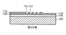
図5Bに示すものは,第1絶縁層102及び第1導線105上に第2絶縁層112を形成し,これをパターニングして第1導線105を露出させる複数のビアホール113を形成した状態を図示したものである。図5Bを参照しながら,第1の実施の形態にかかるインクジェットプリントヘッドを製造する第2工程について説明する。
FIG. 5B illustrates a state in which a second insulating
まず,図5Bに示す第2工程では,第1絶縁層102及び第1導線105上にシリコン酸化膜からなる第2絶縁層112を形成する。次に,前記第2絶縁層112を前述した写真工程及びドライエッチング工程によってパターニングし,導線連結部(図2に示す導線連結部110。)が形成される部分の第1導線105を露出させる複数のビアホール113を形成する。
First, in a second step shown in FIG. 5B, a second insulating
図5Cは,ビアホール(図5Bに示すビアホール113。)及び第2絶縁層112上に複数の導線連結部110及び第2導線106を形成した状態を図示したものである。図5Cを参照しながら,第1の実施の形態にかかるインクジェットプリントヘッドを製造する第3工程について説明する。
FIG. 5C illustrates a state in which a plurality of
まず,図5Cに示す第3工程では,複数のビアホール(図5Bに示すビアホール113。)及び第2絶縁層112上に導電性が良好なアルミニウムやアルミニウム合金などの金属物質を蒸着して金属層を形成する。次に,金属層を前述した写真工程及びエッチング工程によってパターニングし,複数の導線連結部110及び第2導線106を同時に形成する。
First, in a third step shown in FIG. 5C, a metal material having good conductivity, such as aluminum or an aluminum alloy, is deposited on the plurality of via holes (via
図5Dは,第1導線105及び第2導線106を覆うように図5Cに示す結果物の全表面に保護層114を形成した状態を図示したものである。図5Dを参照しながら,第1の実施の形態にかかるインクジェットプリントヘッドを製造する第4工程について説明すると,保護層114は化学気相蒸着法によりシリコン窒化膜(SiN)などを蒸着することにより形成されうる。
FIG. 5D illustrates a state in which a
図5Eは,保護層114上にキャビテーション防止層118を形成した状態を示したものである。図5Eを参照しながら,第1の実施の形態にかかるインクジェットプリントヘッドを製造する第5工程について説明すると,キャビテーション防止層118はスパッタリングにより保護層114上にタンタル薄膜を蒸着させた後,これをパターニングすることにより形成される。
FIG. 5E shows a state in which a
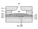
図5Fは,多数の物質層の形成された基板100の上部にインクチャンバ(図2のインクチャンバ120)を限定する隔壁122を形成した状態を図示したものである。図5Fを参照しながら,第1の実施の形態にかかるインクジェットプリントヘッドを製造する第6工程について説明すると,隔壁122は感光性ポリマー,例えばポリイミドを多数の物質層が形成された基板100の上部に所定厚さに塗布した後,これを写真エッチング法によってパターニングすることにより形成されうる。感光性ポリマーの厚さは25〜35μmほどであり,この厚さは吐出されるインク液滴の体積により要求されるインクチャンバ(図2に示すインクチャンバ120)の高さによって決まり,例示された高さとは異なる範囲の高さを有することもある。
FIG. 5F illustrates a state in which a
図5Gは,隔壁122の上部にノズル130が形成されたノズルプレート132を形成した状態を図示したものである。図5Gを参照しながら,第1の実施の形態にかかるインクジェットプリントヘッドを製造する第7工程について説明すると,ノズルプレート132はポリイミドまたはニッケルからなされており,隔壁122をなす感光性ポリマーの接着性を利用して隔壁122上に接着される。
FIG. 5G illustrates a state in which a
一方,図6A〜図6Fは図4に示す第2の実施の形態にかかるインクジェットプリントヘッドを製造する過程を説明するための断面図である。 6A to 6F are cross-sectional views illustrating a process of manufacturing the inkjet print head according to the second embodiment shown in FIG.
まず,基板100上に第1絶縁層102及び第1導線105を形成し,その上に第2絶縁層112及び複数のビアホール(図5Bに示すビアホール113)を形成することは図5A及び図5Bとほぼ同様な構成である。
First, forming a first insulating
次に,図6Aは,第2の実施の形態にかかるビアホール(図5Bに示すビアホール113)に複数の導線連結部210を形成した状態を図示したものである。図6Aを参照しながら,第2の実施の形態にかかるインクジェットプリントヘッドを製造する第1工程について説明する。
Next, FIG. 6A illustrates a state in which a plurality of
具体的に説明すると,導線連結部210は第1導線105を露出させる複数のビアホール(図5Bの113)にTi,TiN,Ta及びTaNのようなバリアメタルを積層し,これをドライエッチングすることにより形成される。
More specifically, the
図6Bは第2絶縁層112及び導線連結部210の上面に第2導線206を形成した状態を図示したものである。図6Bを参照しながら,第2の実施の形態にかかるインクジェットプリントヘッドを製造する第2工程について説明する。
FIG. 6B illustrates a state where the second
具体的には,第2絶縁層及び導線連結部の上面にアルミニウムまたはアルミニウム合金などの金属物質を蒸着して金属層を形成し,これをパターニングして第2導線を形成する。 More specifically, a metal material such as aluminum or an aluminum alloy is deposited on the second insulating layer and the upper surface of the conductor connection part to form a metal layer, and the metal layer is patterned to form a second conductor.
一方,図6C〜図6Fに図示された過程は図5D〜図5Gに図示された過程と,ほぼ同一なのでこれに関わる説明は省略する。 Meanwhile, the processes illustrated in FIGS. 6C to 6F are substantially the same as the processes illustrated in FIGS. 5D to 5G, and a description thereof will be omitted.
以上,添付図面を参照しながら本発明の好適な実施形態について説明したが,本発明はかかる例に限定されない。当業者であれば,特許請求の範囲に記載された技術的思想の範疇内において各種の変更例または修正例を想定し得ることは明らかであり,それらについても当然に本発明の技術的範囲に属するものと了解される。 As described above, the preferred embodiments of the present invention have been described with reference to the accompanying drawings, but the present invention is not limited to such examples. It is obvious that those skilled in the art can envisage various changes or modifications within the scope of the technical idea described in the claims, and those modifications naturally fall within the technical scope of the present invention. It is understood to belong.
上記実施形態においては,インクジェットプリントヘッドの各要素が基板,絶縁層,導線,保護層,キャビテーション防止層等からなる場合を例にあげて説明したが,本発明はかかる例に限定されない。例えば,インクジェットプリントヘッドの各要素を構成するために使われる物質は例示されていない物質が使われても実施することができる。 In the above embodiment, the case where each element of the ink jet print head includes a substrate, an insulating layer, a conductive wire, a protective layer, a cavitation preventing layer, and the like has been described as an example, but the present invention is not limited to this example. For example, the material used to configure each element of the inkjet print head can be implemented even if a material not shown is used.
また,上記実施形態において各段階で例示された具体的な数値は製造されたプリントヘッドが正常に作動できる範囲内でいかようにも例示された範囲を外れて調整可能である。 In addition, the specific values exemplified in each step in the above embodiment can be adjusted outside of the exemplified ranges within a range in which the manufactured print head can normally operate.
また,上記実施形態において,各物質の積層及び形成方法も単に例示されたものであり,多様な積層法が適用されうる。特に,ヒータ部の構造及びこれを形成する方法に主な特徴があるが,その上に積層される隔壁とノズルプレートとは上記説明の方法とは異なる方法により形成される場合でも実施できる。例えば,ノズルプレートは隔壁と同じ物質を利用して一体に形成される場合でもよい。 In addition, in the above-described embodiment, the method of laminating and forming each material is merely an example, and various laminating methods can be applied. In particular, the main features of the structure of the heater portion and the method of forming the heater portion are described. However, the present invention can be implemented even when the partition walls and the nozzle plate laminated thereon are formed by a method different from the above-described method. For example, the nozzle plate may be integrally formed using the same material as the partition.
また,上記実施形態において,第1導線と第2導線の間に配置される導線連結部は,複数個の場合を例に挙げて説明したが,かかる例に限定されない。例えば,導線連結部は,1個の場合であっても実施することができる。 Further, in the above-described embodiment, a case has been described in which a plurality of conductor connection portions are disposed between the first conductor and the second conductor, but the invention is not limited to such an example. For example, the present invention can be practiced with a single conductor connection.
また,上記実施形態において,第1導線と第2導線の間には,上記導線連結部同士を絶縁するために第2絶縁層が備えられる場合を例に挙げて説明したが,かかる例に限定されず,例えば,上記第2絶縁層を備えない場合であっても実施することができる。 Further, in the above embodiment, the case where the second insulating layer is provided between the first conductor and the second conductor to insulate the conductor coupling portions from each other has been described as an example, but the invention is not limited to this example. However, for example, the present invention can be implemented even when the above-mentioned second insulating layer is not provided.
本発明は,印刷用インクの微小な液滴を記録用紙上の所望する位置に吐出させて所定色相の画像に印刷するインクジェットプリントヘッドに適用可能である。 INDUSTRIAL APPLICABILITY The present invention is applicable to an ink jet print head that discharges minute droplets of printing ink to a desired position on a recording sheet and prints an image of a predetermined hue.
100 基板
102,112 第1及び2絶縁層
104 ヒータ部
105,106 第1及び第2導線
110 導線連結部
110a 第1接面部
114 保護層
118 キャビテーション防止層
120 インクチャンバ
122 隔壁
130 ノズル
132 ノズルプレート
DESCRIPTION OF
Claims (10)
前記基板の表面に形成された第1絶縁層と;
前記第1絶縁層上に上下に互いに離隔した状態で形成される第1導線及び第2導線と;
前記第1導線と第2導線との間に,前記第1導線と第2導線を電気的に連結する1又は2以上の導線連結部を少なくとも含むヒータ部と;
前記第1導線と第2導線との間に形成され,前記1又は2以上の導線連結部を絶縁するための第2絶縁層と;
前記基板の上部に設けられ,吐出されるインクが満たされるインクチャンバを形成するための隔壁と;
前記隔壁の上部に設けられて前記インクチャンバの上部壁をなし,前記インクチャンバに満たされたインクを吐出するためのノズルが形成されたノズルプレートとを備えることを特徴とする,インクジェットプリントヘッド。 A substrate;
A first insulating layer formed on a surface of the substrate;
A first conductive wire and a second conductive wire formed on the first insulating layer so as to be vertically separated from each other;
A heater unit between the first conductor and the second conductor, the heater unit including at least one or more conductor connection parts for electrically connecting the first conductor and the second conductor;
A second insulating layer formed between the first conductor and the second conductor, for insulating the one or more conductor coupling parts;
A partition wall provided on the substrate for forming an ink chamber filled with ink to be ejected;
An ink jet print head, comprising: a nozzle plate provided above the partition wall, forming an upper wall of the ink chamber, and having a nozzle for discharging ink filled in the ink chamber.
(b)前記第1絶縁層上に第1導線を形成する段階と;
(c)前記第1絶縁層及び前記第1導線上に第2絶縁層を形成し,パターニングして前記第1導線を露出させる複数のビアホールを形成する段階と;
(d)前記ビアホール及び前記第2絶縁層上に1又は2以上の導線連結部と,第2導線を形成する段階と;
(e)前記第1及び第2導線を覆うように前記基板の全面に保護層を形成する段階と;
(f)前記保護層上にキャビテーション防止層を形成する段階と;
(g)前記基板の上部にインクチャンバの隔壁を形成する段階と;
(h)前記隔壁上に,前記インクチャンバからインクを吐出するためのノズルが形成されたノズルプレートを形成する段階とを含むことを特徴とする,インクジェットプリントヘッドの製造方法。 (A) forming a first insulating layer on a surface of the substrate;
(B) forming a first conductive line on the first insulating layer;
(C) forming a second insulating layer on the first insulating layer and the first conductive line and patterning to form a plurality of via holes exposing the first conductive line;
(D) forming one or more conductor connection portions on the via hole and the second insulating layer, and forming a second conductor;
(E) forming a protective layer on the entire surface of the substrate so as to cover the first and second conductive lines;
(F) forming an anti-cavitation layer on the protective layer;
(G) forming a partition of an ink chamber on the substrate;
(H) forming a nozzle plate having nozzles for discharging ink from the ink chamber on the partition walls.
Applications Claiming Priority (1)
| Application Number | Priority Date | Filing Date | Title |
|---|---|---|---|
| KR10-2002-0081863A KR100472485B1 (en) | 2002-12-20 | 2002-12-20 | Inkjet printhead and manufacturing method thereof |
Publications (2)
| Publication Number | Publication Date |
|---|---|
| JP2004203049A true JP2004203049A (en) | 2004-07-22 |
| JP4107496B2 JP4107496B2 (en) | 2008-06-25 |
Family
ID=32709698
Family Applications (1)
| Application Number | Title | Priority Date | Filing Date |
|---|---|---|---|
| JP2003425225A Expired - Fee Related JP4107496B2 (en) | 2002-12-20 | 2003-12-22 | Ink jet print head and manufacturing method thereof |
Country Status (4)
| Country | Link |
|---|---|
| US (1) | US7018019B2 (en) |
| JP (1) | JP4107496B2 (en) |
| KR (1) | KR100472485B1 (en) |
| CN (1) | CN100349742C (en) |
Families Citing this family (4)
| Publication number | Priority date | Publication date | Assignee | Title |
|---|---|---|---|---|
| JP4617145B2 (en) * | 2003-12-16 | 2011-01-19 | キヤノン株式会社 | Manufacturing method of substrate for liquid discharge head |
| KR100723414B1 (en) * | 2005-12-07 | 2007-05-30 | 삼성전자주식회사 | Thermally driven type inkjet printhead |
| JP5404121B2 (en) * | 2009-03-25 | 2014-01-29 | キヤノン株式会社 | Recording substrate, method for manufacturing the recording substrate, and liquid discharge head |
| CN108773186B (en) * | 2018-08-14 | 2023-10-27 | 北京捷润科技有限公司 | Spray head protection device and protection method |
Family Cites Families (6)
| Publication number | Priority date | Publication date | Assignee | Title |
|---|---|---|---|---|
| US4513298A (en) * | 1983-05-25 | 1985-04-23 | Hewlett-Packard Company | Thermal ink jet printhead |
| US4990939A (en) * | 1988-09-01 | 1991-02-05 | Ricoh Company, Ltd. | Bubble jet printer head with improved operational speed |
| JP3559701B2 (en) * | 1997-12-18 | 2004-09-02 | キヤノン株式会社 | Substrate for inkjet recording head, method for manufacturing the substrate, inkjet recording head, and inkjet recording apparatus |
| JPH11291531A (en) * | 1998-04-03 | 1999-10-26 | Sony Corp | Recorder and manufacture thereof |
| US6293654B1 (en) * | 1998-04-22 | 2001-09-25 | Hewlett-Packard Company | Printhead apparatus |
| EP1142967B1 (en) * | 2000-03-30 | 2008-12-24 | Hewlett-Packard Company | Jet printing ink |
-
2002
- 2002-12-20 KR KR10-2002-0081863A patent/KR100472485B1/en not_active IP Right Cessation
-
2003
- 2003-10-23 US US10/690,820 patent/US7018019B2/en not_active Expired - Fee Related
- 2003-12-02 CN CNB2003101187337A patent/CN100349742C/en not_active Expired - Fee Related
- 2003-12-22 JP JP2003425225A patent/JP4107496B2/en not_active Expired - Fee Related
Also Published As
| Publication number | Publication date |
|---|---|
| CN100349742C (en) | 2007-11-21 |
| US20040135850A1 (en) | 2004-07-15 |
| US7018019B2 (en) | 2006-03-28 |
| KR20040055230A (en) | 2004-06-26 |
| JP4107496B2 (en) | 2008-06-25 |
| KR100472485B1 (en) | 2005-03-09 |
| CN1509875A (en) | 2004-07-07 |
Similar Documents
| Publication | Publication Date | Title |
|---|---|---|
| US8109609B2 (en) | Ink ejecting device and method of manufacturing the same | |
| EP1908593A1 (en) | Inkjet printhead and method of manufaturing the same | |
| JP2002079679A (en) | Ink jet printing head and method of fabricating the same | |
| US8191998B2 (en) | Liquid ejecting head | |
| KR100433528B1 (en) | Inkjet printhead and manufacturing method thereof | |
| KR100425306B1 (en) | Bubble-jet type inkjet printhead | |
| KR100856412B1 (en) | Method of manufacturing inkjet printhead | |
| JP4107496B2 (en) | Ink jet print head and manufacturing method thereof | |
| JP2004237732A (en) | Ink jet printhead and method for manufacturing the same | |
| KR20100011652A (en) | Inkjet printhead and method of manufacturing the same | |
| KR20080114358A (en) | Method of manufacturing inkjet printhead | |
| US20090267996A1 (en) | Heater stack with enhanced protective strata structure and methods for making enhanced heater stack | |
| CN108136776B (en) | Fluid ejection apparatus | |
| US20090141083A1 (en) | Inkjet printhead and method of manufacturing the same | |
| KR100723415B1 (en) | Method of fabricating inkjet printhead | |
| JP7191669B2 (en) | SUBSTRATE FOR LIQUID EJECTION HEAD AND MANUFACTURING METHOD THEREOF | |
| KR100553912B1 (en) | Inkjet printhead and method for manufacturing the same | |
| JP2004142462A (en) | Inkjet printhead and its manufacturing method | |
| KR100519765B1 (en) | Inkjet printhead and manufacturing method the same | |
| KR100497389B1 (en) | Inkjet printhead and method of manufacturing thereof | |
| JP7286349B2 (en) | LIQUID EJECTION HEAD SUBSTRATE, LIQUID EJECTION HEAD SUBSTRATE MANUFACTURING METHOD, AND LIQUID EJECTION HEAD | |
| CN110406258B (en) | Liquid ejection head substrate, method of manufacturing liquid ejection head substrate, and liquid ejection head | |
| KR100484202B1 (en) | Inkjet printhead with reverse heater and method of manufacturing thereof | |
| KR100421027B1 (en) | Inkjet printhead and manufacturing method thereof | |
| KR100438726B1 (en) | Ink jet print head and manufacturing method thereof |
Legal Events
| Date | Code | Title | Description |
|---|---|---|---|
| A131 | Notification of reasons for refusal |
Free format text: JAPANESE INTERMEDIATE CODE: A131 Effective date: 20070116 |
|
| A521 | Written amendment |
Free format text: JAPANESE INTERMEDIATE CODE: A523 Effective date: 20070411 |
|
| A131 | Notification of reasons for refusal |
Free format text: JAPANESE INTERMEDIATE CODE: A131 Effective date: 20070515 |
|
| A521 | Written amendment |
Free format text: JAPANESE INTERMEDIATE CODE: A523 Effective date: 20070814 |
|
| A131 | Notification of reasons for refusal |
Free format text: JAPANESE INTERMEDIATE CODE: A131 Effective date: 20071030 |
|
| A521 | Written amendment |
Free format text: JAPANESE INTERMEDIATE CODE: A523 Effective date: 20080129 |
|
| TRDD | Decision of grant or rejection written | ||
| A01 | Written decision to grant a patent or to grant a registration (utility model) |
Free format text: JAPANESE INTERMEDIATE CODE: A01 Effective date: 20080304 |
|
| A61 | First payment of annual fees (during grant procedure) |
Free format text: JAPANESE INTERMEDIATE CODE: A61 Effective date: 20080327 |
|
| FPAY | Renewal fee payment (event date is renewal date of database) |
Free format text: PAYMENT UNTIL: 20110411 Year of fee payment: 3 |
|
| R150 | Certificate of patent or registration of utility model |
Free format text: JAPANESE INTERMEDIATE CODE: R150 |
|
| LAPS | Cancellation because of no payment of annual fees |