JP2004186461A - Manufacturing method of circuit unit - Google Patents
Manufacturing method of circuit unit Download PDFInfo
- Publication number
- JP2004186461A JP2004186461A JP2002352141A JP2002352141A JP2004186461A JP 2004186461 A JP2004186461 A JP 2004186461A JP 2002352141 A JP2002352141 A JP 2002352141A JP 2002352141 A JP2002352141 A JP 2002352141A JP 2004186461 A JP2004186461 A JP 2004186461A
- Authority
- JP
- Japan
- Prior art keywords
- wiring layer
- conductive wiring
- resin
- conductive film
- conductive
- Prior art date
- Legal status (The legal status is an assumption and is not a legal conclusion. Google has not performed a legal analysis and makes no representation as to the accuracy of the status listed.)
- Granted
Links
Images


Classifications
-
- H—ELECTRICITY
- H01—ELECTRIC ELEMENTS
- H01L—SEMICONDUCTOR DEVICES NOT COVERED BY CLASS H10
- H01L24/00—Arrangements for connecting or disconnecting semiconductor or solid-state bodies; Methods or apparatus related thereto
- H01L24/93—Batch processes
- H01L24/95—Batch processes at chip-level, i.e. with connecting carried out on a plurality of singulated devices, i.e. on diced chips
- H01L24/97—Batch processes at chip-level, i.e. with connecting carried out on a plurality of singulated devices, i.e. on diced chips the devices being connected to a common substrate, e.g. interposer, said common substrate being separable into individual assemblies after connecting
-
- H—ELECTRICITY
- H01—ELECTRIC ELEMENTS
- H01L—SEMICONDUCTOR DEVICES NOT COVERED BY CLASS H10
- H01L21/00—Processes or apparatus adapted for the manufacture or treatment of semiconductor or solid state devices or of parts thereof
- H01L21/02—Manufacture or treatment of semiconductor devices or of parts thereof
- H01L21/04—Manufacture or treatment of semiconductor devices or of parts thereof the devices having at least one potential-jump barrier or surface barrier, e.g. PN junction, depletion layer or carrier concentration layer
- H01L21/48—Manufacture or treatment of parts, e.g. containers, prior to assembly of the devices, using processes not provided for in a single one of the subgroups H01L21/06 - H01L21/326
- H01L21/4814—Conductive parts
- H01L21/4846—Leads on or in insulating or insulated substrates, e.g. metallisation
-
- H—ELECTRICITY
- H01—ELECTRIC ELEMENTS
- H01L—SEMICONDUCTOR DEVICES NOT COVERED BY CLASS H10
- H01L23/00—Details of semiconductor or other solid state devices
- H01L23/28—Encapsulations, e.g. encapsulating layers, coatings, e.g. for protection
- H01L23/31—Encapsulations, e.g. encapsulating layers, coatings, e.g. for protection characterised by the arrangement or shape
- H01L23/3107—Encapsulations, e.g. encapsulating layers, coatings, e.g. for protection characterised by the arrangement or shape the device being completely enclosed
- H01L23/3121—Encapsulations, e.g. encapsulating layers, coatings, e.g. for protection characterised by the arrangement or shape the device being completely enclosed a substrate forming part of the encapsulation
- H01L23/3128—Encapsulations, e.g. encapsulating layers, coatings, e.g. for protection characterised by the arrangement or shape the device being completely enclosed a substrate forming part of the encapsulation the substrate having spherical bumps for external connection
-
- H—ELECTRICITY
- H01—ELECTRIC ELEMENTS
- H01L—SEMICONDUCTOR DEVICES NOT COVERED BY CLASS H10
- H01L23/00—Details of semiconductor or other solid state devices
- H01L23/48—Arrangements for conducting electric current to or from the solid state body in operation, e.g. leads, terminal arrangements ; Selection of materials therefor
- H01L23/488—Arrangements for conducting electric current to or from the solid state body in operation, e.g. leads, terminal arrangements ; Selection of materials therefor consisting of soldered or bonded constructions
- H01L23/498—Leads, i.e. metallisations or lead-frames on insulating substrates, e.g. chip carriers
- H01L23/49866—Leads, i.e. metallisations or lead-frames on insulating substrates, e.g. chip carriers characterised by the materials
- H01L23/49894—Materials of the insulating layers or coatings
-
- H—ELECTRICITY
- H01—ELECTRIC ELEMENTS
- H01L—SEMICONDUCTOR DEVICES NOT COVERED BY CLASS H10
- H01L2224/00—Indexing scheme for arrangements for connecting or disconnecting semiconductor or solid-state bodies and methods related thereto as covered by H01L24/00
- H01L2224/01—Means for bonding being attached to, or being formed on, the surface to be connected, e.g. chip-to-package, die-attach, "first-level" interconnects; Manufacturing methods related thereto
- H01L2224/26—Layer connectors, e.g. plate connectors, solder or adhesive layers; Manufacturing methods related thereto
- H01L2224/31—Structure, shape, material or disposition of the layer connectors after the connecting process
- H01L2224/32—Structure, shape, material or disposition of the layer connectors after the connecting process of an individual layer connector
- H01L2224/321—Disposition
- H01L2224/32151—Disposition the layer connector connecting between a semiconductor or solid-state body and an item not being a semiconductor or solid-state body, e.g. chip-to-substrate, chip-to-passive
- H01L2224/32221—Disposition the layer connector connecting between a semiconductor or solid-state body and an item not being a semiconductor or solid-state body, e.g. chip-to-substrate, chip-to-passive the body and the item being stacked
- H01L2224/32225—Disposition the layer connector connecting between a semiconductor or solid-state body and an item not being a semiconductor or solid-state body, e.g. chip-to-substrate, chip-to-passive the body and the item being stacked the item being non-metallic, e.g. insulating substrate with or without metallisation
-
- H—ELECTRICITY
- H01—ELECTRIC ELEMENTS
- H01L—SEMICONDUCTOR DEVICES NOT COVERED BY CLASS H10
- H01L2224/00—Indexing scheme for arrangements for connecting or disconnecting semiconductor or solid-state bodies and methods related thereto as covered by H01L24/00
- H01L2224/01—Means for bonding being attached to, or being formed on, the surface to be connected, e.g. chip-to-package, die-attach, "first-level" interconnects; Manufacturing methods related thereto
- H01L2224/42—Wire connectors; Manufacturing methods related thereto
- H01L2224/44—Structure, shape, material or disposition of the wire connectors prior to the connecting process
- H01L2224/45—Structure, shape, material or disposition of the wire connectors prior to the connecting process of an individual wire connector
- H01L2224/45001—Core members of the connector
- H01L2224/45099—Material
- H01L2224/451—Material with a principal constituent of the material being a metal or a metalloid, e.g. boron (B), silicon (Si), germanium (Ge), arsenic (As), antimony (Sb), tellurium (Te) and polonium (Po), and alloys thereof
-
- H—ELECTRICITY
- H01—ELECTRIC ELEMENTS
- H01L—SEMICONDUCTOR DEVICES NOT COVERED BY CLASS H10
- H01L2224/00—Indexing scheme for arrangements for connecting or disconnecting semiconductor or solid-state bodies and methods related thereto as covered by H01L24/00
- H01L2224/01—Means for bonding being attached to, or being formed on, the surface to be connected, e.g. chip-to-package, die-attach, "first-level" interconnects; Manufacturing methods related thereto
- H01L2224/42—Wire connectors; Manufacturing methods related thereto
- H01L2224/47—Structure, shape, material or disposition of the wire connectors after the connecting process
- H01L2224/48—Structure, shape, material or disposition of the wire connectors after the connecting process of an individual wire connector
- H01L2224/4805—Shape
- H01L2224/4809—Loop shape
- H01L2224/48091—Arched
-
- H—ELECTRICITY
- H01—ELECTRIC ELEMENTS
- H01L—SEMICONDUCTOR DEVICES NOT COVERED BY CLASS H10
- H01L2224/00—Indexing scheme for arrangements for connecting or disconnecting semiconductor or solid-state bodies and methods related thereto as covered by H01L24/00
- H01L2224/01—Means for bonding being attached to, or being formed on, the surface to be connected, e.g. chip-to-package, die-attach, "first-level" interconnects; Manufacturing methods related thereto
- H01L2224/42—Wire connectors; Manufacturing methods related thereto
- H01L2224/47—Structure, shape, material or disposition of the wire connectors after the connecting process
- H01L2224/48—Structure, shape, material or disposition of the wire connectors after the connecting process of an individual wire connector
- H01L2224/481—Disposition
- H01L2224/48151—Connecting between a semiconductor or solid-state body and an item not being a semiconductor or solid-state body, e.g. chip-to-substrate, chip-to-passive
- H01L2224/48221—Connecting between a semiconductor or solid-state body and an item not being a semiconductor or solid-state body, e.g. chip-to-substrate, chip-to-passive the body and the item being stacked
- H01L2224/48225—Connecting between a semiconductor or solid-state body and an item not being a semiconductor or solid-state body, e.g. chip-to-substrate, chip-to-passive the body and the item being stacked the item being non-metallic, e.g. insulating substrate with or without metallisation
- H01L2224/48227—Connecting between a semiconductor or solid-state body and an item not being a semiconductor or solid-state body, e.g. chip-to-substrate, chip-to-passive the body and the item being stacked the item being non-metallic, e.g. insulating substrate with or without metallisation connecting the wire to a bond pad of the item
-
- H—ELECTRICITY
- H01—ELECTRIC ELEMENTS
- H01L—SEMICONDUCTOR DEVICES NOT COVERED BY CLASS H10
- H01L2224/00—Indexing scheme for arrangements for connecting or disconnecting semiconductor or solid-state bodies and methods related thereto as covered by H01L24/00
- H01L2224/01—Means for bonding being attached to, or being formed on, the surface to be connected, e.g. chip-to-package, die-attach, "first-level" interconnects; Manufacturing methods related thereto
- H01L2224/42—Wire connectors; Manufacturing methods related thereto
- H01L2224/47—Structure, shape, material or disposition of the wire connectors after the connecting process
- H01L2224/48—Structure, shape, material or disposition of the wire connectors after the connecting process of an individual wire connector
- H01L2224/481—Disposition
- H01L2224/48151—Connecting between a semiconductor or solid-state body and an item not being a semiconductor or solid-state body, e.g. chip-to-substrate, chip-to-passive
- H01L2224/48221—Connecting between a semiconductor or solid-state body and an item not being a semiconductor or solid-state body, e.g. chip-to-substrate, chip-to-passive the body and the item being stacked
- H01L2224/48245—Connecting between a semiconductor or solid-state body and an item not being a semiconductor or solid-state body, e.g. chip-to-substrate, chip-to-passive the body and the item being stacked the item being metallic
- H01L2224/48247—Connecting between a semiconductor or solid-state body and an item not being a semiconductor or solid-state body, e.g. chip-to-substrate, chip-to-passive the body and the item being stacked the item being metallic connecting the wire to a bond pad of the item
-
- H—ELECTRICITY
- H01—ELECTRIC ELEMENTS
- H01L—SEMICONDUCTOR DEVICES NOT COVERED BY CLASS H10
- H01L2224/00—Indexing scheme for arrangements for connecting or disconnecting semiconductor or solid-state bodies and methods related thereto as covered by H01L24/00
- H01L2224/01—Means for bonding being attached to, or being formed on, the surface to be connected, e.g. chip-to-package, die-attach, "first-level" interconnects; Manufacturing methods related thereto
- H01L2224/42—Wire connectors; Manufacturing methods related thereto
- H01L2224/47—Structure, shape, material or disposition of the wire connectors after the connecting process
- H01L2224/48—Structure, shape, material or disposition of the wire connectors after the connecting process of an individual wire connector
- H01L2224/484—Connecting portions
- H01L2224/48463—Connecting portions the connecting portion on the bonding area of the semiconductor or solid-state body being a ball bond
- H01L2224/48465—Connecting portions the connecting portion on the bonding area of the semiconductor or solid-state body being a ball bond the other connecting portion not on the bonding area being a wedge bond, i.e. ball-to-wedge, regular stitch
-
- H—ELECTRICITY
- H01—ELECTRIC ELEMENTS
- H01L—SEMICONDUCTOR DEVICES NOT COVERED BY CLASS H10
- H01L2224/00—Indexing scheme for arrangements for connecting or disconnecting semiconductor or solid-state bodies and methods related thereto as covered by H01L24/00
- H01L2224/01—Means for bonding being attached to, or being formed on, the surface to be connected, e.g. chip-to-package, die-attach, "first-level" interconnects; Manufacturing methods related thereto
- H01L2224/42—Wire connectors; Manufacturing methods related thereto
- H01L2224/47—Structure, shape, material or disposition of the wire connectors after the connecting process
- H01L2224/49—Structure, shape, material or disposition of the wire connectors after the connecting process of a plurality of wire connectors
- H01L2224/491—Disposition
- H01L2224/4912—Layout
- H01L2224/49171—Fan-out arrangements
-
- H—ELECTRICITY
- H01—ELECTRIC ELEMENTS
- H01L—SEMICONDUCTOR DEVICES NOT COVERED BY CLASS H10
- H01L2224/00—Indexing scheme for arrangements for connecting or disconnecting semiconductor or solid-state bodies and methods related thereto as covered by H01L24/00
- H01L2224/73—Means for bonding being of different types provided for in two or more of groups H01L2224/10, H01L2224/18, H01L2224/26, H01L2224/34, H01L2224/42, H01L2224/50, H01L2224/63, H01L2224/71
- H01L2224/732—Location after the connecting process
- H01L2224/73251—Location after the connecting process on different surfaces
- H01L2224/73265—Layer and wire connectors
-
- H—ELECTRICITY
- H01—ELECTRIC ELEMENTS
- H01L—SEMICONDUCTOR DEVICES NOT COVERED BY CLASS H10
- H01L2224/00—Indexing scheme for arrangements for connecting or disconnecting semiconductor or solid-state bodies and methods related thereto as covered by H01L24/00
- H01L2224/80—Methods for connecting semiconductor or other solid state bodies using means for bonding being attached to, or being formed on, the surface to be connected
- H01L2224/85—Methods for connecting semiconductor or other solid state bodies using means for bonding being attached to, or being formed on, the surface to be connected using a wire connector
- H01L2224/85909—Post-treatment of the connector or wire bonding area
- H01L2224/8591—Cleaning, e.g. oxide removal step, desmearing
- H01L2224/85913—Plasma cleaning
-
- H—ELECTRICITY
- H01—ELECTRIC ELEMENTS
- H01L—SEMICONDUCTOR DEVICES NOT COVERED BY CLASS H10
- H01L2224/00—Indexing scheme for arrangements for connecting or disconnecting semiconductor or solid-state bodies and methods related thereto as covered by H01L24/00
- H01L2224/93—Batch processes
- H01L2224/95—Batch processes at chip-level, i.e. with connecting carried out on a plurality of singulated devices, i.e. on diced chips
- H01L2224/97—Batch processes at chip-level, i.e. with connecting carried out on a plurality of singulated devices, i.e. on diced chips the devices being connected to a common substrate, e.g. interposer, said common substrate being separable into individual assemblies after connecting
-
- H—ELECTRICITY
- H01—ELECTRIC ELEMENTS
- H01L—SEMICONDUCTOR DEVICES NOT COVERED BY CLASS H10
- H01L24/00—Arrangements for connecting or disconnecting semiconductor or solid-state bodies; Methods or apparatus related thereto
- H01L24/01—Means for bonding being attached to, or being formed on, the surface to be connected, e.g. chip-to-package, die-attach, "first-level" interconnects; Manufacturing methods related thereto
- H01L24/42—Wire connectors; Manufacturing methods related thereto
- H01L24/44—Structure, shape, material or disposition of the wire connectors prior to the connecting process
- H01L24/45—Structure, shape, material or disposition of the wire connectors prior to the connecting process of an individual wire connector
-
- H—ELECTRICITY
- H01—ELECTRIC ELEMENTS
- H01L—SEMICONDUCTOR DEVICES NOT COVERED BY CLASS H10
- H01L24/00—Arrangements for connecting or disconnecting semiconductor or solid-state bodies; Methods or apparatus related thereto
- H01L24/01—Means for bonding being attached to, or being formed on, the surface to be connected, e.g. chip-to-package, die-attach, "first-level" interconnects; Manufacturing methods related thereto
- H01L24/42—Wire connectors; Manufacturing methods related thereto
- H01L24/47—Structure, shape, material or disposition of the wire connectors after the connecting process
- H01L24/48—Structure, shape, material or disposition of the wire connectors after the connecting process of an individual wire connector
-
- H—ELECTRICITY
- H01—ELECTRIC ELEMENTS
- H01L—SEMICONDUCTOR DEVICES NOT COVERED BY CLASS H10
- H01L24/00—Arrangements for connecting or disconnecting semiconductor or solid-state bodies; Methods or apparatus related thereto
- H01L24/01—Means for bonding being attached to, or being formed on, the surface to be connected, e.g. chip-to-package, die-attach, "first-level" interconnects; Manufacturing methods related thereto
- H01L24/42—Wire connectors; Manufacturing methods related thereto
- H01L24/47—Structure, shape, material or disposition of the wire connectors after the connecting process
- H01L24/49—Structure, shape, material or disposition of the wire connectors after the connecting process of a plurality of wire connectors
-
- H—ELECTRICITY
- H01—ELECTRIC ELEMENTS
- H01L—SEMICONDUCTOR DEVICES NOT COVERED BY CLASS H10
- H01L24/00—Arrangements for connecting or disconnecting semiconductor or solid-state bodies; Methods or apparatus related thereto
- H01L24/73—Means for bonding being of different types provided for in two or more of groups H01L24/10, H01L24/18, H01L24/26, H01L24/34, H01L24/42, H01L24/50, H01L24/63, H01L24/71
-
- H—ELECTRICITY
- H01—ELECTRIC ELEMENTS
- H01L—SEMICONDUCTOR DEVICES NOT COVERED BY CLASS H10
- H01L2924/00—Indexing scheme for arrangements or methods for connecting or disconnecting semiconductor or solid-state bodies as covered by H01L24/00
- H01L2924/01—Chemical elements
- H01L2924/01005—Boron [B]
-
- H—ELECTRICITY
- H01—ELECTRIC ELEMENTS
- H01L—SEMICONDUCTOR DEVICES NOT COVERED BY CLASS H10
- H01L2924/00—Indexing scheme for arrangements or methods for connecting or disconnecting semiconductor or solid-state bodies as covered by H01L24/00
- H01L2924/01—Chemical elements
- H01L2924/01006—Carbon [C]
-
- H—ELECTRICITY
- H01—ELECTRIC ELEMENTS
- H01L—SEMICONDUCTOR DEVICES NOT COVERED BY CLASS H10
- H01L2924/00—Indexing scheme for arrangements or methods for connecting or disconnecting semiconductor or solid-state bodies as covered by H01L24/00
- H01L2924/01—Chemical elements
- H01L2924/0101—Neon [Ne]
-
- H—ELECTRICITY
- H01—ELECTRIC ELEMENTS
- H01L—SEMICONDUCTOR DEVICES NOT COVERED BY CLASS H10
- H01L2924/00—Indexing scheme for arrangements or methods for connecting or disconnecting semiconductor or solid-state bodies as covered by H01L24/00
- H01L2924/01—Chemical elements
- H01L2924/01011—Sodium [Na]
-
- H—ELECTRICITY
- H01—ELECTRIC ELEMENTS
- H01L—SEMICONDUCTOR DEVICES NOT COVERED BY CLASS H10
- H01L2924/00—Indexing scheme for arrangements or methods for connecting or disconnecting semiconductor or solid-state bodies as covered by H01L24/00
- H01L2924/01—Chemical elements
- H01L2924/01018—Argon [Ar]
-
- H—ELECTRICITY
- H01—ELECTRIC ELEMENTS
- H01L—SEMICONDUCTOR DEVICES NOT COVERED BY CLASS H10
- H01L2924/00—Indexing scheme for arrangements or methods for connecting or disconnecting semiconductor or solid-state bodies as covered by H01L24/00
- H01L2924/01—Chemical elements
- H01L2924/01029—Copper [Cu]
-
- H—ELECTRICITY
- H01—ELECTRIC ELEMENTS
- H01L—SEMICONDUCTOR DEVICES NOT COVERED BY CLASS H10
- H01L2924/00—Indexing scheme for arrangements or methods for connecting or disconnecting semiconductor or solid-state bodies as covered by H01L24/00
- H01L2924/01—Chemical elements
- H01L2924/01033—Arsenic [As]
-
- H—ELECTRICITY
- H01—ELECTRIC ELEMENTS
- H01L—SEMICONDUCTOR DEVICES NOT COVERED BY CLASS H10
- H01L2924/00—Indexing scheme for arrangements or methods for connecting or disconnecting semiconductor or solid-state bodies as covered by H01L24/00
- H01L2924/01—Chemical elements
- H01L2924/01046—Palladium [Pd]
-
- H—ELECTRICITY
- H01—ELECTRIC ELEMENTS
- H01L—SEMICONDUCTOR DEVICES NOT COVERED BY CLASS H10
- H01L2924/00—Indexing scheme for arrangements or methods for connecting or disconnecting semiconductor or solid-state bodies as covered by H01L24/00
- H01L2924/01—Chemical elements
- H01L2924/01047—Silver [Ag]
-
- H—ELECTRICITY
- H01—ELECTRIC ELEMENTS
- H01L—SEMICONDUCTOR DEVICES NOT COVERED BY CLASS H10
- H01L2924/00—Indexing scheme for arrangements or methods for connecting or disconnecting semiconductor or solid-state bodies as covered by H01L24/00
- H01L2924/01—Chemical elements
- H01L2924/01078—Platinum [Pt]
-
- H—ELECTRICITY
- H01—ELECTRIC ELEMENTS
- H01L—SEMICONDUCTOR DEVICES NOT COVERED BY CLASS H10
- H01L2924/00—Indexing scheme for arrangements or methods for connecting or disconnecting semiconductor or solid-state bodies as covered by H01L24/00
- H01L2924/01—Chemical elements
- H01L2924/01079—Gold [Au]
-
- H—ELECTRICITY
- H01—ELECTRIC ELEMENTS
- H01L—SEMICONDUCTOR DEVICES NOT COVERED BY CLASS H10
- H01L2924/00—Indexing scheme for arrangements or methods for connecting or disconnecting semiconductor or solid-state bodies as covered by H01L24/00
- H01L2924/01—Chemical elements
- H01L2924/01082—Lead [Pb]
-
- H—ELECTRICITY
- H01—ELECTRIC ELEMENTS
- H01L—SEMICONDUCTOR DEVICES NOT COVERED BY CLASS H10
- H01L2924/00—Indexing scheme for arrangements or methods for connecting or disconnecting semiconductor or solid-state bodies as covered by H01L24/00
- H01L2924/06—Polymers
- H01L2924/078—Adhesive characteristics other than chemical
- H01L2924/07802—Adhesive characteristics other than chemical not being an ohmic electrical conductor
-
- H—ELECTRICITY
- H01—ELECTRIC ELEMENTS
- H01L—SEMICONDUCTOR DEVICES NOT COVERED BY CLASS H10
- H01L2924/00—Indexing scheme for arrangements or methods for connecting or disconnecting semiconductor or solid-state bodies as covered by H01L24/00
- H01L2924/10—Details of semiconductor or other solid state devices to be connected
- H01L2924/11—Device type
- H01L2924/12—Passive devices, e.g. 2 terminal devices
- H01L2924/1204—Optical Diode
- H01L2924/12042—LASER
-
- H—ELECTRICITY
- H01—ELECTRIC ELEMENTS
- H01L—SEMICONDUCTOR DEVICES NOT COVERED BY CLASS H10
- H01L2924/00—Indexing scheme for arrangements or methods for connecting or disconnecting semiconductor or solid-state bodies as covered by H01L24/00
- H01L2924/10—Details of semiconductor or other solid state devices to be connected
- H01L2924/11—Device type
- H01L2924/13—Discrete devices, e.g. 3 terminal devices
- H01L2924/1304—Transistor
- H01L2924/1305—Bipolar Junction Transistor [BJT]
- H01L2924/13055—Insulated gate bipolar transistor [IGBT]
-
- H—ELECTRICITY
- H01—ELECTRIC ELEMENTS
- H01L—SEMICONDUCTOR DEVICES NOT COVERED BY CLASS H10
- H01L2924/00—Indexing scheme for arrangements or methods for connecting or disconnecting semiconductor or solid-state bodies as covered by H01L24/00
- H01L2924/10—Details of semiconductor or other solid state devices to be connected
- H01L2924/11—Device type
- H01L2924/14—Integrated circuits
-
- H—ELECTRICITY
- H01—ELECTRIC ELEMENTS
- H01L—SEMICONDUCTOR DEVICES NOT COVERED BY CLASS H10
- H01L2924/00—Indexing scheme for arrangements or methods for connecting or disconnecting semiconductor or solid-state bodies as covered by H01L24/00
- H01L2924/15—Details of package parts other than the semiconductor or other solid state devices to be connected
- H01L2924/151—Die mounting substrate
- H01L2924/153—Connection portion
- H01L2924/1531—Connection portion the connection portion being formed only on the surface of the substrate opposite to the die mounting surface
- H01L2924/15311—Connection portion the connection portion being formed only on the surface of the substrate opposite to the die mounting surface being a ball array, e.g. BGA
-
- H—ELECTRICITY
- H01—ELECTRIC ELEMENTS
- H01L—SEMICONDUCTOR DEVICES NOT COVERED BY CLASS H10
- H01L2924/00—Indexing scheme for arrangements or methods for connecting or disconnecting semiconductor or solid-state bodies as covered by H01L24/00
- H01L2924/15—Details of package parts other than the semiconductor or other solid state devices to be connected
- H01L2924/181—Encapsulation
-
- H—ELECTRICITY
- H01—ELECTRIC ELEMENTS
- H01L—SEMICONDUCTOR DEVICES NOT COVERED BY CLASS H10
- H01L2924/00—Indexing scheme for arrangements or methods for connecting or disconnecting semiconductor or solid-state bodies as covered by H01L24/00
- H01L2924/19—Details of hybrid assemblies other than the semiconductor or other solid state devices to be connected
- H01L2924/1901—Structure
- H01L2924/1904—Component type
- H01L2924/19041—Component type being a capacitor
-
- H—ELECTRICITY
- H01—ELECTRIC ELEMENTS
- H01L—SEMICONDUCTOR DEVICES NOT COVERED BY CLASS H10
- H01L2924/00—Indexing scheme for arrangements or methods for connecting or disconnecting semiconductor or solid-state bodies as covered by H01L24/00
- H01L2924/19—Details of hybrid assemblies other than the semiconductor or other solid state devices to be connected
- H01L2924/1901—Structure
- H01L2924/1904—Component type
- H01L2924/19043—Component type being a resistor
-
- H—ELECTRICITY
- H01—ELECTRIC ELEMENTS
- H01L—SEMICONDUCTOR DEVICES NOT COVERED BY CLASS H10
- H01L2924/00—Indexing scheme for arrangements or methods for connecting or disconnecting semiconductor or solid-state bodies as covered by H01L24/00
- H01L2924/30—Technical effects
- H01L2924/35—Mechanical effects
- H01L2924/351—Thermal stress
-
- H—ELECTRICITY
- H05—ELECTRIC TECHNIQUES NOT OTHERWISE PROVIDED FOR
- H05K—PRINTED CIRCUITS; CASINGS OR CONSTRUCTIONAL DETAILS OF ELECTRIC APPARATUS; MANUFACTURE OF ASSEMBLAGES OF ELECTRICAL COMPONENTS
- H05K3/00—Apparatus or processes for manufacturing printed circuits
- H05K3/22—Secondary treatment of printed circuits
- H05K3/28—Applying non-metallic protective coatings
- H05K3/284—Applying non-metallic protective coatings for encapsulating mounted components
-
- H—ELECTRICITY
- H05—ELECTRIC TECHNIQUES NOT OTHERWISE PROVIDED FOR
- H05K—PRINTED CIRCUITS; CASINGS OR CONSTRUCTIONAL DETAILS OF ELECTRIC APPARATUS; MANUFACTURE OF ASSEMBLAGES OF ELECTRICAL COMPONENTS
- H05K3/00—Apparatus or processes for manufacturing printed circuits
- H05K3/38—Improvement of the adhesion between the insulating substrate and the metal
- H05K3/381—Improvement of the adhesion between the insulating substrate and the metal by special treatment of the substrate
-
- Y—GENERAL TAGGING OF NEW TECHNOLOGICAL DEVELOPMENTS; GENERAL TAGGING OF CROSS-SECTIONAL TECHNOLOGIES SPANNING OVER SEVERAL SECTIONS OF THE IPC; TECHNICAL SUBJECTS COVERED BY FORMER USPC CROSS-REFERENCE ART COLLECTIONS [XRACs] AND DIGESTS
- Y10—TECHNICAL SUBJECTS COVERED BY FORMER USPC
- Y10T—TECHNICAL SUBJECTS COVERED BY FORMER US CLASSIFICATION
- Y10T29/00—Metal working
- Y10T29/49—Method of mechanical manufacture
- Y10T29/49002—Electrical device making
- Y10T29/49117—Conductor or circuit manufacturing
- Y10T29/49124—On flat or curved insulated base, e.g., printed circuit, etc.
- Y10T29/49128—Assembling formed circuit to base
-
- Y—GENERAL TAGGING OF NEW TECHNOLOGICAL DEVELOPMENTS; GENERAL TAGGING OF CROSS-SECTIONAL TECHNOLOGIES SPANNING OVER SEVERAL SECTIONS OF THE IPC; TECHNICAL SUBJECTS COVERED BY FORMER USPC CROSS-REFERENCE ART COLLECTIONS [XRACs] AND DIGESTS
- Y10—TECHNICAL SUBJECTS COVERED BY FORMER USPC
- Y10T—TECHNICAL SUBJECTS COVERED BY FORMER US CLASSIFICATION
- Y10T29/00—Metal working
- Y10T29/49—Method of mechanical manufacture
- Y10T29/49002—Electrical device making
- Y10T29/49117—Conductor or circuit manufacturing
- Y10T29/49124—On flat or curved insulated base, e.g., printed circuit, etc.
- Y10T29/4913—Assembling to base an electrical component, e.g., capacitor, etc.
- Y10T29/49144—Assembling to base an electrical component, e.g., capacitor, etc. by metal fusion
-
- Y—GENERAL TAGGING OF NEW TECHNOLOGICAL DEVELOPMENTS; GENERAL TAGGING OF CROSS-SECTIONAL TECHNOLOGIES SPANNING OVER SEVERAL SECTIONS OF THE IPC; TECHNICAL SUBJECTS COVERED BY FORMER USPC CROSS-REFERENCE ART COLLECTIONS [XRACs] AND DIGESTS
- Y10—TECHNICAL SUBJECTS COVERED BY FORMER USPC
- Y10T—TECHNICAL SUBJECTS COVERED BY FORMER US CLASSIFICATION
- Y10T29/00—Metal working
- Y10T29/49—Method of mechanical manufacture
- Y10T29/49002—Electrical device making
- Y10T29/49117—Conductor or circuit manufacturing
- Y10T29/49124—On flat or curved insulated base, e.g., printed circuit, etc.
- Y10T29/49155—Manufacturing circuit on or in base
- Y10T29/49165—Manufacturing circuit on or in base by forming conductive walled aperture in base
Landscapes
- Engineering & Computer Science (AREA)
- Microelectronics & Electronic Packaging (AREA)
- Computer Hardware Design (AREA)
- Power Engineering (AREA)
- Condensed Matter Physics & Semiconductors (AREA)
- General Physics & Mathematics (AREA)
- Physics & Mathematics (AREA)
- Manufacturing & Machinery (AREA)
- Ceramic Engineering (AREA)
- Production Of Multi-Layered Print Wiring Board (AREA)
- Encapsulation Of And Coatings For Semiconductor Or Solid State Devices (AREA)
- Non-Metallic Protective Coatings For Printed Circuits (AREA)
- Manufacturing Of Printed Wiring (AREA)
Abstract
Description
【0001】
【発明の属する技術分野】
本発明は回路装置の製造方法に関し、特に、プラズマを用いて回路装置を構成する要素同士の密着を向上させる回路装置の製造方法に関する。
【0002】
【従来の技術】
近年、ICパッケージは携帯機器や小型・高密度実装機器への採用が進み、従来のICパッケージとその実装概念が大きく変わろうとしている。絶縁樹脂シートの一例としてフレキシブルシートであるポリイミド樹脂シートを採用した半導体装置に関する技術がある(例えば、特許文献1参照)。
【0003】
図13は、フレキシブルシート50をインターポーザー基板として採用する半導体装置を示すものである。図13(A)はこの半導体装置の平面図であり、図13(B)は、図13(A)のA−A線における断面図である。以下にてこの半導体装置の製造方法を説明する。
【0004】
先ず、フレキシブルシート50の上には、接着剤を介して銅箔パターン51が貼り合わされて用意されている。この銅箔パターン51は、実装される半導体素子がトランジスタ、ICにより、そのパターンが異なるが、一般には、ボンディングパッド51A、アイランド51Bが形成されている。また符号52は、フレキシブルシート50の裏面から電極を取り出すための開口部であり、前記銅箔パターン51が露出している。続いて、このフレキシブルシート50は、ダイボンダーに搬送され、半導体素子53が実装される。その後、このフレキシブルシート50は、ワイヤーボンダーに搬送され、ボンディングパッド51Aと半導体素子53のパッドが金属細線54で電気的に接続されている。
【0005】
最後に、図13(A)の如く、フレキシブルシート50の表面に封止樹脂層55が設けられて封止される。ここでは、ボンディングパッド51A、アイランド51B、半導体素子53および金属細線54を被覆するようにトランスファーモールドされる。その後、図13(B)に示すように、半田や半田ボール等の接続手段56が設けられ、半田リフロー炉を通過することで開口部52を介してボンディングパッド51Aと融着した球状の半田56が形成される。その後、フレキシブルシート50には、半導体素子53がマトリックス状に形成されるため、ダイシングされ、個々に分離される。
【0006】
しかしながら、図13を参照して説明した半導体装置の製造方法は、フレキシブルシート50を採用しているために、様々な問題を有していた。即ち、フレキシブルシート50自身が有る程度の厚みを有しているので装置の薄型化に限界があり、製造工程に於いてフレキシブルシート50にクラックが発生したり、フレキシブルシート50に反りが発生してしまうという数々の問題を有していた。
【0007】
上記のような問題を解決するために、フレキシブルシート50等のようなインターポーザー基板を不要にした薄型の回路装置およびその製造方法が提案されている(例えば特許文献2を参照)。
【0008】
図14を参照して、この回路装置60の概要を説明する。回路装置60は、フレキシブルシート等のインターポーザを不要にして構成されている。そして、絶縁樹脂62の表裏にシート状に接着された導電膜をエッチングすることにより、第1の導電配線層63および第2の導電配線層64から成る多層配線構造が実現されている。第1の導電配線層63および第2の導電配線層64は、層間絶縁層62により絶縁され、多層接続手段72により所望の箇所で電気的に接続されている。また、第2の導電配線層64の所望の箇所には外部電極74が形成され、これは実装基板等との接続電極となる。第1の導電配線層63上には、オーバーコート樹脂76がパッドとなる箇所を除いて塗布されており、絶縁性接着剤68を介して半導体素子67が固着されており、半導体素子67の電極と第1の導電配線層63とは金属細線71により電気的に接続されている。封止樹脂層73は、半導体素子67および金属細線71を封止して全体の機械的な支持を行う働きを有する。
【0009】
上記した回路装置60は、フレキシブルシート等のインターポーザを不要にして構成されており、このことにより、装置全体が薄型化されている等の利点を有する。
【0010】
また、金属から成るパターンの表面に付着した汚染物質の除去等を行う技術として、プラズマ照射の技術がある。図15を参照して、半導体装置が実装されたリードフレームにプラズマを照射して、表面に付着した汚染物質を除去する方法を説明する。
【0011】
図15(A)を参照して、リードフレームの加工を行う工程および素子の実装工程等を経たリードフレーム110の構成を説明する。ランド状に形成されたアイランド114には半導体素子112が実装され、アイランド114を囲むように多数個のリード111が設けられている。また、リード111は半導体素子112の表面に設けた電極に対応しており、金属細線113を介して各電極はリードと電気的に接続されている。
【0012】
図15(B)を参照して、プラズマ照射を行う工程を説明する。先ず、密閉された容器内部にリードフレーム110を載置する。次に、容器内部にガスを導入して、放電によりプラズマガスを生成する。そしてプラズマガス中に存在するラジカルまたはイオンが、リードフレーム110の表面に衝突することによりリードフレーム110表面の洗浄が行われる。
【0013】
【特許文献1】
特開2000−133678号公報(第5頁、第2図)
【特許文献2】
特願2001−185420(第1図)
【0014】
【発明が解決しようとする課題】
しかしながら、上記した回路装置60では、第1の導電配線層を被覆するオーバーコート樹脂76と封止樹脂層73との密着性が充分でなく、使用状況下の温度変化により発生する熱応力により、両者の界面にクラックが発生してしまう問題があった。更にオーバーコート樹脂76と封止樹脂層73との界面から外気に含まれる水分等が回路装置内部に進入してしまう等の問題もあった。
【0015】
また、図15に示したようなプラズマ照射によるリードフレームの洗浄方法では、アイランド114やリード111が形成されるように複雑な形状に加工されているため、プラズマ照射によりリードフレーム110に局所的な電位の増加が発生する。このことから、リードフレームの局所的な電位差により、金属細線113を介して半導体素子112に電流が流れ込み、半導体素子表面に形成されたCMOS等の素子が破壊されてしまう問題があった。更に、プラズマ照射の工程でリードフレーム110が高温となることから、リードが変形して、金属細線113が断線してしまう問題があった。
【0016】
本発明はこのような問題を鑑みて成されたものであり、本発明の主な目的は、プラズマ照射を用いて、回路装置を構成する要素同士の密着力を向上させる回路装置の製造方法を提供することにある。
【0017】
【課題を解決するための手段】
本発明は、層間絶縁層を介して多層に積層された導電膜を設ける工程と、表面の前記導電膜を選択的に除去して導電配線層を形成する工程と、前記層間絶縁層に貫通孔を形成して前記貫通孔に接続手段を形成することにより前記導電配線層と裏面の前記導電膜を電気的に接続する工程と、回路素子を固着して前記導電配線層と電気的に接続する工程と、前記回路素子も含めて前記導電配線層にプラズマを照射する工程と、前記回路素子を被覆するように樹脂層を形成する工程とを有することを特徴とする。導電配線層をプラズマ照射により粗化させることにより、導電配線層と樹脂部材との密着を向上させることができる。
【0018】
更に、導電配線層上に樹脂が形成された場合は、樹脂を粗化させることにより、樹脂層と樹脂との密着性を向上させることが可能となる。また、導電配線層は、電気的に連結されているので、プラズマの照射により樹脂にチャージアップされる電圧は、導電配線層および導電膜を介して外部に逃がされる。従って、プラズマを照射する工程に於いて局所的な電位差の発生を抑制することができるので、半導体素子等の回路素子が破壊されるのを抑制することができる。
【0019】
【発明の実施の形態】
本発明の回路装置の製造方法は、層間絶縁層22を介して多層に積層された導電膜23を設ける工程と、表面の導電膜23を選択的に除去して導電配線層12を形成する工程と、層間絶縁層22に貫通孔31を形成して貫通孔31に接続手段14を形成することにより導電配線層12と裏面の導電膜23を電気的に接続する工程と、回路素子13を固着して裏面の導電配線層12と電気的に接続する工程と、回路素子13も含めて導電配線層12にプラズマを照射する工程と、回路素子13を被覆するように封止樹脂層17を形成する工程とを有する。
このような各工程を以下にて説明する。
【0020】
本発明の第1の工程は、図1から図3に示すように、層間絶縁層22を介して多層に積層された導電膜23を用意し、導電膜23を選択的に除去して導電配線層12を形成し、層間絶縁層22に貫通孔31を形成して貫通孔31に接続手段14を形成することにより導電配線層12と導電膜23を電気的に接続する工程である。
【0021】
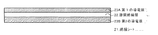
本工程では、先ず、第1の導電膜23Aおよび第2の導電膜23Bが層間絶縁層22を介して積層された絶縁シート21を設ける。ここで、層間絶縁層22の材料としては、例えば、ガラスエポキシ樹脂、レジン系樹脂または液晶ポリマーが挙げられる。絶縁シート21の表面は、実質全域に第1の導電膜23Aが形成され、裏面にも実質全域に第2の導電膜23Bが形成されるものである。層間絶縁層22の材料は、熱可塑性樹脂または熱硬化性樹脂を採用することができる。また、第1の導電膜23Aおよび第2の導電膜23Bは、好ましくは、Cuを主材料とするもの、または公知のリードフレームの材料であり、メッキ法、蒸着法またはスパッタ法で層間絶縁層22に被覆されたり、圧延法やメッキ法により形成された金属箔が貼着されても良い。また絶縁シート21は、キャスティング法で形成されても良い。以下に簡単にその製造方法を述べる。まず平膜状の第1の導電膜23Aの上に糊状の絶縁性樹脂を塗布し、また平膜状の第2の導電膜23Bの上にも糊状の絶縁性樹脂を塗布する。そして両者の樹脂を半硬化させた後に貼り合わせると絶縁シート21ができあがる。
【0022】
ペースト状のものを塗ってシートとするキャスティング法の場合、その膜厚は、10μm〜100μm程度である。またシートとして形成する場合、市販のものは25μmが最小の膜厚である。また熱伝導性が考慮され、中にフィラーが混入されても良い。材料としては、ガラス、酸化Si、酸化アルミニウム、窒化Al、Siカーバイド、窒化ボロン等が考えられる。
【0023】
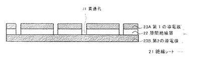
図2を参照して、次に、絶縁シート21の所望個所に第1の導電膜23Aおよび層間絶縁層22に貫通孔31を形成し、第2の導電膜23Bを選択的に露出させる。具体的には、第1の導電膜23Aの貫通孔31を形成する部分だけを露出してホトレジストで全面を被覆する。そしてこのホトレジストを介して第1の導電膜23Aをエッチングする。第1の導電膜23AはCuを主材料とするものであるので、エッチング液は、塩化第2鉄または塩化第2銅を用いてケミカルエッチングを行う。貫通孔31の開口径は、ホトリソグラフィーの解像度により変化するが、ここでは50〜100μm程度である。またこのエッチングの際に、第2の導電膜23Bは接着性のシート等でカバーしてエッチング液から保護する。しかし第2の導電膜23B自体が十分に厚く、エッチング後にも平坦性が維持できる膜厚であれば、少々エッチングされても構わない。
【0024】
続いて、ホトレジストを取り除いた後、第1の導電膜23Aをマスクにして、レーザーにより貫通孔31の真下の層間絶縁層22を取り除き、貫通孔31の底に第2の導電膜23Bを露出させる。レーザーとしては、炭酸ガスレーザーが好ましい。またレーザーで絶縁樹脂を蒸発させた後、開口部の底部に残査がある場合は、過マンガン酸ソーダまたは過硫酸アンモニウム等でウェットエッチングし、この残査を取り除く。
【0025】
図3を参照して、次に、貫通孔31を含む第1の導電膜23A全面に第2の導電膜23Bと第1の導電膜23Aの電気的接続を行う多層接続手段14であるメッキ膜を形成する。このメッキ膜は無電解メッキと電解メッキの両方で形成され、ここでは、無電解メッキにより約2μmのCuを少なくとも貫通孔31を含む第1の導電膜23A全面に形成する。これにより第1の導電膜23Aと第2の導電膜23Bが電気的に導通するため、再度この第1および第2導電膜23A、23Bを電極にして電解メッキを行い、約20μmのCuをメッキする。これにより貫通孔31はCuで埋め込まれ、多層接続手段14が形成される。またメッキ膜は、ここではCuを採用したが、Au、Ag、Pd等を採用しても良い。またマスクを使用して部分メッキをしても良い。
【0026】
次に、図3を参照して、第1の導電膜23Aを所望のパターンにエッチングして第1の導電配線層12Aを形成する。第1の導電膜23A上に所望のパターンのホトレジストで被覆し、図11に示すような配線を形成する場合は、ボンディングパッド部およびそこから中央に延在される第1の導電配線層12Aをケミカルエッチングにより形成する。第1の導電膜23AはCuを主材料とするものであるので、エッチング液は、塩化第2鉄または塩化第2銅を用いれば良い。
【0027】
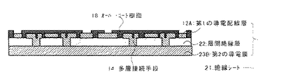
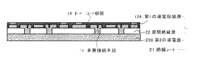
本発明の第2の工程は、図4および図5に示す如く、パッドとなる箇所を露出させて表面の導電配線層12をオーバーコート樹脂18で被覆する工程である。図4を参照して、オーバーコート樹脂18は溶剤で溶かしたエポキシ樹脂等をスクリーン印刷で付着し、熱硬化させる。または、樹脂から成るドライフィルムを貼り付ける。ここで使用する樹脂としては、熱硬化性樹脂または熱可塑性樹脂を使用することができる。また、オーバーコート樹脂18の材料としては感光性の樹脂または非感光性の樹脂を使用することができる。更に、ボンディングパッドとなる箇所の導電配線層を露出させるために、その上部のオーバーコート樹脂は部分的に除去される。
次に、図5に示す如く、ボンディングパッド上にはボンディング性を考慮して、Au、Ag等のメッキ膜が形成される。このメッキ膜はオーバーコート樹脂18をマスクとしてボンディングパッド上に選択的に無電界メッキで付着されるか、また第2の導電膜23Bを電極として電界メッキで付着される。
【0028】
本発明の第3の工程は、図6を参照して、オーバーコート樹脂18上に回路素子13を固着して導電配線層12と電気的に接続する工程である。
【0029】
回路素子13は、ここでは半導体素子であり、ベアチップのままオーバーコート樹脂18上に絶縁性接着樹脂等を介してダイボンドされる。回路素子13とその下の第1の導電配線層12Aとはオーバーコート樹脂18で電気的に絶縁されるので、第1の導電配線層12Aは回路素子13の下でも自由に配線でき、多層配線構造を実現できる。
【0030】
また、回路素子13の各電極パッドは周辺に設けた第1の導電配線層12Aの一部であるボンデイングパッドに金属細線15で接続されている。ここで、回路素子13はフェイスダウンで実装されても良い。この場合、回路素子13の各電極パッド表面に半田ボールやバンプが設けられ、第1の導電配線層12Aの表面には半田ボールの位置に対応した部分にボンディングパッドと同様の電極が設けられる。
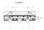
【0031】
本発明の第4の工程は、図7を参照して、回路素子13も含めてオーバーコート樹脂18の表面にプラズマを照射し、オーバーコート樹脂18にチャージアップされる電圧を導電配線層12から導電膜23を介して逃がしながらオーバーコート樹脂18の表面を粗化する工程である。図7(A)はプラズマ洗浄を行う概要を示す図であり、図7(B)は1つの搭載部15にプラズマ照射を行う様子を示す断面図である。
【0032】
図7(A)を参照して、プラズマ洗浄機30は、密閉容器34の内部に設けた上段電極31と、上段電極31に対向して設けられて上部に絶縁シート21が載置される下段電極31とを有している。また、ガスを容器内部に供給する注入口35と、その排気を行う排気口36が設けられている。上段電極31と下段電極32のどちらかは、高周波電源と接続されており、電源と接続されない電極は接地されている。
【0033】
導電箔表面の汚染物質を行うプラズマ洗浄は、化学的エッチングと物理的エッチングの2つの方法がある。化学的エッチングにはDP(Direct Plazma)またはPE(Plazma Etching)が含まれ、ガスとして酸素を使用することができる。物理・化学的エッチングにはRIE(Reactive Ion Etching)が含まれ、ガスとしてアルゴン、ネオンまたはヘリウム等の不活性ガスを使用することができる。化学的エッチングでは化学的効果を使用して有機物の汚染物質の除去および表面の粗化をすることができ、物理的エッチングではスパッタ効果で有機物および無機物の汚染物質の除去および表面の粗化を行うことができる。本発明では、どちらの手法も用いることが可能である。また、オゾンを用いてプラズマ照射を行うことも可能である。
【0034】
図7(B)を参照して、プラズマによる表面粗化の詳細を説明する。本発明では、プラズマの照射は、絶縁シート21の全域に渡って行われる。具体的には、放電により生成されたプラズマ33の中のイオンを、絶縁シート21の表面全域に衝突させている。従って、オーバーコート樹脂18、回路素子13および金属細線15にイオンが衝突して、それらの表面には微細な凹凸が形成されて粗化される。また、それらの表面に付着した有機性または無機性の汚染物質は除去される。
【0035】
また、第1の導電配線層12Aは、最下層の導電膜である第2の導電膜23Bにより電気的に一体となっている。従って、プラズマの影響下に晒されても、オーバーコート樹脂18に蓄積される電荷により発生する電圧は、第1の導電配線層12Aおよび第2の導電膜を介して外部に逃がされる。このことから、回路素子13が電圧破壊し易いCMOS等であっても、回路素子13に与えるダメージを最小に抑制することができる。
【0036】
また、アルゴンを用いるRIEによりプラズマ照射を行う場合は、アルゴンのイオンエネルギーを40eV〜100eVの範囲に成るように設定する。このことにより、表面の付着物は除去され、表面の適度な粗化と洗浄化を行うことができる。
【0037】
更にまた、上記したDPとRIEを組み合わせてプラズマ照射を行うこともできる。この場合は、酸素ガスを用いたDPを行った後に、不活性ガスを用いたRIEを行う。このことにより、DPを行うことにより表面に形成された酸化膜をRIEにより適度に除去することができる。
【0038】
絶縁シート21は、最下層の第2の導電膜23Bにより機械的に支持されている。従って、本工程により、絶縁シート21が加熱されても、絶縁シート21は均一に熱膨張を行うので、第1の導電配線層12Aの局所的な熱膨張や変形は防止される。従って、第1の導電配線層12Aの膨張や変形による金属細線15の折れ曲がりや断線を抑止することができる。
【0039】
第1の導電配線層12Aがオーバーコート樹脂18で被覆された状態でプラズマ照射を行うことの利点を説明する。第1の導電配線層12Aはその角部も含めて、オーバーコート樹脂18により被覆されている。従って、プラズマ照射を行うことにより、第1の導電配線層12Aの角部からスパークが発生するのを防止することができる。このことから、スパークの集中により、導電配線層12Aの材料である銅が蒸散してしまうのを防止することができる。更に、蒸散した材料により、プラズマ洗浄機30内が汚染されてしまうのを防止することもできる。
【0040】
本発明の第5の工程は、図8を参照して、回路素子13およびオーバーコート樹脂18の表面を被覆するように封止樹脂層17を形成する工程である。
【0041】
絶縁シート21は、モールド装置にセットされて樹脂モールドを行う。モールド方法としては、トランスファーモールド、インジェクションモールド、塗布、ディピング等でも可能である。本発明では、熱可塑性樹脂を用いたトランスファーモールドで樹脂封止をおこなっている。オーバーコート樹脂18は前工程でその表面が粗化されているので、オーバーコート樹脂18の表面と封止樹脂層17との密着性は向上される。
【0042】
また、図8(A)を参照して、本工程では、モールドキャビティーの下金型に絶縁シート21はフラットで当接される必要があるが、厚い第2の導電膜23Bがこの働きをする。しかもモールドキャビティーから取り出した後も、封止樹脂層17の収縮が完全に完了するまで、第2の導電膜23Bによってパッケージの平坦性を維持している。すなわち、本工程までの絶縁シート21の機械的支持の役割は第2の導電膜23Bにより担われている。
【0043】
図8(B)を参照して、更に本工程では、絶縁シート21上にマトリックス状に多数個の回路素子13が固着されたブロックを形成しており、このブロックが1つのモールド金型で共通モールドされる。同図では、1枚の絶縁シート21に複数個(ここでは4個)のブロックが離間して設けられ、各ブロックが1つの封止樹脂層17で樹脂封止されている。従って、1つの金型を用いて多数個の回路装置をモールドすることが可能となり、製造される回路装置の大きさや形状に応じて金型を新たに作成するコストを省くことが可能となり、更に、使用する樹脂量を削減することができる。
【0044】
更に、本工程では、モールドキャビティーの下金型に絶縁シート21はフラットで当接される必要があるが、厚い第2の導電膜23Bがこの働きをする。しかもモールドキャビティーから取り出した後も、封止樹脂層層17の収縮が完全に完了するまで、第2の導電膜23Bによってパッケージの平坦性を維持している。すなわち、本工程までの絶縁シート21の機械的支持の役割は第2の導電膜23Bにより担われている。
【0045】
本発明の第6の工程は、図9を参照して、第2の導電膜23Bを選択的に除去することにより、第2の導電配線層12Bを形成することにある。
【0046】
第2の導電膜23Bは、所望のパターンのホトレジストで被覆し、ケミカルエッチングで第2の導電配線層12Bを形成する。例えば、第2の導電配線層12Bは図11に示すように一定の間隔で配列され、個々は第1の導電配線層12Aと多層接続手段14を介して電気的に接続されて多層配線構造を実現している。
【0047】
次に、第2の導電配線層15は外部電極16を形成する部分を露出して溶剤で溶かしたエポキシ樹脂等をスクリーン印刷してオーバーコート樹脂18で大部分を被覆する。次に半田のリフローによりこの露出部分に外部電極16を同時に形成する。最後に、絶縁シート21には回路装置が多数マトリックス状に形成されているので、封止樹脂層層17および絶縁シート21をダイシングしてそれらを個々の回路装置に分離する。
【0048】
また、第2の導電膜23Bは全面的に除去することも可能である。この場合は、層間絶縁層11の裏面から多層接続手段14が露出し、露出した多層接続手段14に外部電極が形成される。
【0049】
図10および図11を参照して、上記した工程で製造される回路装置10の構成を説明する。回路装置10は、層間絶縁層11を介して積層された第1の導電配線層12Aおよび第2の導電配線層12Bと、前記第1の導電配線層12Aを被覆するオーバーコート樹脂18と、オーバーコート樹脂18上に固着されて第1の導電配線層12Aと電気的に接続される回路素子13と、回路素子13を被覆する封止樹脂層層17と、前記両導電配線層12同士を所望の個所で層間絶縁層11を貫通して接続する多層接続手段14と、第2の導電配線層12Bの所望個所に設けた外部電極16とから成る構成と成っている。このような構成要素を以下にて説明する。
【0050】
第1の導電配線層12Aおよび第2の導電配線層12Bは、層間絶縁層11の表裏に形成された導電膜をエッチングすることにより形成されている。導電膜の材料は、好ましくは、Cuを主材料とするもの、または公知のリードフレームの材料であり、メッキ法、蒸着法またはスパッタ法で層間絶縁層11に被覆されたり、圧延法やメッキ法により形成された金属箔が貼着されても良い。また、第1の導電配線層12Aおよび第2の導電配線層12Bは、オーバーコート樹脂18で被覆されている。
【0051】
層間絶縁層11は、第1の導電配線層12Aと第2の導電配線層12Bとを絶縁する働きを有し、両導電配線層12の間の層として設けられている。層間絶縁層11の材料としては、高温時に軟化する特性を有する熱可塑性樹脂または熱硬化性樹脂が採用される。
【0052】
オーバーコート樹脂18は、熱硬化性樹脂または熱可塑性樹脂から成り、第1の導電配線層12Aの大部分を被覆している。また、回路素子13との接続を行うパッドとなる箇所のオーバーコート樹脂18は部分的に除去され、メッキ膜が形成されている。ここでは、オーバーコート樹脂18の表面は、前述したプラズマ照射を行う工程で粗化されており、粗化されたオーバーコート樹脂18の表面と封止樹脂層17との密着は強固になっている。
【0053】
回路素子13は、絶縁性接着剤等を介して第1の導電配線層12A上に固着されており、第1の導電配線層12Aとは金属細線15を介して電気的に接続されている。本実施の形態では、回路素子13としては、2つの半導体素子が固着されている。また、回路素子13としては、半導体素子以外の回路素子を採用することも可能であり、チップコンデンサ、チップ抵抗またはトランジスタチップ等も回路素子13として採用することができる。
【0054】
多層接続手段14は第1の導電配線層12Aと第2の導電配線層12Bとを所望の個所で層間絶縁層11を貫通して接続している。多層配線手段14としては具体的には銅のメッキ膜が適している。また金、銀、パラジュウム等のメッキ膜でも良い。
【0055】
封止樹脂層層17は第1の導電配線層12Aおよび回路素子13を被覆している。この封止樹脂層層17は完成した回路装置全体の機械的支持の働きも兼用している。また、封止樹脂層層17はトランスファーモールドにより形成される熱硬化性樹脂から形成されている。
【0056】
外部電極16は第2の導電配線層12Bの所望個所に設けられる。すなわち、第2の導電配線層12Bの大部分はオーバーコート樹脂18で被覆され、露出した第2の導電配線層12B上に半田等のロウ材で形成された外部電極16を設ける。
【0057】
図11を参照して、本発明の回路装置10の平面的な構造の一例を説明する。まず、実線で示すパターンは第1の導電配線層12Aであり、点線で示すパターンは第2の導電配線層12Bである。第1の導電配線層12Aは回路素子13を取り巻くようにボンディングパッドを形成し、一部では2段に配置されて多パッドを有する回路素子13に対応している。第1の導電配線層12Aは回路素子13の対応する電極パッドと金属細線15で接続され、ファインパターンに形成された第1の導電配線層12Aが回路素子13の下に多数延在されて、黒丸で示す多層接続手段14で第2の導電配線層12Bと接続されている。
【0058】
斯かる構造であれば、200以上パッドを有する半導体素子でも、第1の導電配線層12Aのファインパターンを利用して所望の第2の導電配線層12Bまで多層配線構造で延在でき、第2の導電配線層12Bに設けられた外部電極から外部回路への接続が行える。
【0059】
また、同図を参照して、周辺部の第1の導電配線層12Aには、回路素子13Aが実装されている。ここで、回路素子13Aとしては、チップ抵抗やチップコンデンサ等の受動部品や、ベアのトランジスタチップやダイオード等の能動部品を採用することができる。このように、最外周部に回路素子13Aを実装することにより、装置全体の実装密度を向上させることができる。
【0060】
図12を参照して、3層の配線構造を有する回路装置10の構成を説明する。同図を参照して説明する回路装置の基本的な構成は、図10を参照して説明したものと同様であり、その相違点は導電配線層12にある。ここでは、第1の導電配線層12A、第2の導電配線層12Bおよび第3の導電配線層12Cから成る3層の配線構造が形成されている。また、最上層の導電パターンである第1の導電配線層12Aは、その大部分がオーバーコート樹脂18で被覆されている。そして、オーバーコート樹脂18の表面はプラズマ処理が施されることにより、その表面は粗面となり、オーバーコート樹脂18と封止樹脂層17との密着性は向上されている。
【0061】
本発明の回路装置の製造方法によると、最下層の導電膜23で全体の導電配線層12が電気的に一体にされた状態でプラズマ洗浄を行うので、プラズマの影響によりオーバーコート樹脂18に発生する電圧を導電膜を介して外部に逃がすことができる。従って、プラズマの影響で発生した電位差により回路素子13に与えるダメージを抑制することができる。
【0062】
更に、プラズマ照射を行うことにより、導電配線層12を被覆するオーバーコート樹脂18の表面は粗化されるので、オーバーコート樹脂18と封止樹脂層17との密着性は向上される。
【0063】
更にまた、導電配線層12が形成された絶縁シート21は、最下層の導電膜23で機械的に支持され、プラズマ照射により加熱されても全体が均一に熱膨張をするので、局所的な導電配線層12の熱変形による金属細線15の折れ曲がりや断線を防止することができる。
【0064】
【発明の効果】
本発明に依れば、プラズマ照射を用いて、回路装置を構成する要素同士の密着力を向上させて、回路装置の信頼性を向上させることができる。
【図面の簡単な説明】
【図1】本発明の回路装置の製造方法を説明する断面図である。
【図2】本発明の回路装置の製造方法を説明する断面図である。
【図3】本発明の回路装置の製造方法を説明する断面図である。
【図4】本発明の回路装置の製造方法を説明する断面図である。
【図5】本発明の回路装置の製造方法を説明する断面図である。
【図6】本発明の回路装置の製造方法を説明する断面図である。
【図7】本発明の回路装置の製造方法を説明する断面図(A)、断面図(B)である。
【図8】本発明の回路装置の製造方法を説明する断面図(A)、平面図(B)である。
【図9】本発明の回路装置の製造方法を説明する断面図である。
【図10】本発明の回路装置の製造方法を説明する断面図である。
【図11】本発明の回路装置の製造方法を説明する平面図である。
【図12】本発明の回路装置の製造方法を説明する断面図である。
【図13】従来の回路装置の製造方法を説明する平面図(A)、断面図(B)である。
【図14】従来の回路装置の製造方法を説明する断面図である。
【図15】従来の回路装置の製造方法を説明する平面図(A)、断面図(B)である。
【符号の説明】
10 回路装置
12A 第1の導電配線層
12B 第2の導電配線層
13 回路素子
14 多層接続手段
15 金属細線
16 外部電極
17 封止樹脂層層
18 オーバーコート樹脂
22 層間絶縁層
23A 第1の導電膜
23B 第2の導電膜[0001]
TECHNICAL FIELD OF THE INVENTION
The present invention relates to a method for manufacturing a circuit device, and more particularly, to a method for manufacturing a circuit device that improves the adhesion between elements constituting the circuit device using plasma.
[0002]
[Prior art]
In recent years, the adoption of IC packages in portable devices and small-sized / high-density mounting devices has been advanced, and the concept of mounting the conventional IC packages and that of the conventional IC packages is about to change significantly. As an example of the insulating resin sheet, there is a technology relating to a semiconductor device employing a polyimide resin sheet which is a flexible sheet (for example, see Patent Document 1).
[0003]
FIG. 13 shows a semiconductor device employing the flexible sheet 50 as an interposer substrate. FIG. 13A is a plan view of the semiconductor device, and FIG. 13B is a cross-sectional view taken along line AA of FIG. 13A. Hereinafter, a method for manufacturing the semiconductor device will be described.
[0004]
First, a
[0005]
Finally, as shown in FIG. 13A, a sealing
[0006]
However, the method for manufacturing a semiconductor device described with reference to FIG. 13 has various problems because the flexible sheet 50 is employed. That is, since the flexible sheet 50 itself has a certain thickness, there is a limit to the reduction in the thickness of the device, and the flexible sheet 50 may be cracked or warped in the manufacturing process. Had many problems.
[0007]
In order to solve the above-described problems, a thin circuit device that does not require an interposer substrate such as the flexible sheet 50 and the like and a method of manufacturing the same have been proposed (for example, see Patent Document 2).
[0008]
The outline of the circuit device 60 will be described with reference to FIG. The circuit device 60 does not require an interposer such as a flexible sheet. Then, by etching the conductive film adhered to the front and back of the insulating resin 62 in a sheet shape, a multilayer wiring structure including the first conductive wiring layer 63 and the second
[0009]
The above-described circuit device 60 is configured without the need for an interposer such as a flexible sheet, and has the advantage that the entire device is made thinner.
[0010]
As a technique for removing contaminants attached to the surface of a metal pattern, there is a technique of plasma irradiation. Referring to FIG. 15, a method for irradiating a lead frame on which a semiconductor device is mounted with plasma to remove contaminants attached to the surface will be described.
[0011]
With reference to FIG. 15A, a configuration of the lead frame 110 that has undergone a step of processing a lead frame and a step of mounting elements will be described. A
[0012]
The step of performing plasma irradiation will be described with reference to FIG. First, the lead frame 110 is placed inside a sealed container. Next, a gas is introduced into the container, and a plasma gas is generated by discharge. Then, the radicals or ions present in the plasma gas collide with the surface of the lead frame 110, thereby cleaning the surface of the lead frame 110.
[0013]
[Patent Document 1]
JP-A-2000-133678 (page 5, FIG. 2)
[Patent Document 2]
Japanese Patent Application No. 2001-185420 (FIG. 1)
[0014]
[Problems to be solved by the invention]
However, in the above-described circuit device 60, the adhesion between the
[0015]
In the method of cleaning the lead frame by plasma irradiation as shown in FIG. 15, since the lead 114 is processed into a complicated shape so as to form the island 114 and the lead 111, the lead frame 110 is locally irradiated with the plasma. An increase in potential occurs. For this reason, there is a problem that a current flows into the
[0016]
The present invention has been made in view of such a problem, and a main object of the present invention is to provide a method of manufacturing a circuit device that improves the adhesion between elements constituting the circuit device by using plasma irradiation. To provide.
[0017]
[Means for Solving the Problems]
The present invention provides a step of providing a multilayered conductive film via an interlayer insulating layer, a step of selectively removing the conductive film on the surface to form a conductive wiring layer, and a step of forming a through hole in the interlayer insulating layer. Forming a connection means in the through-hole to electrically connect the conductive wiring layer and the conductive film on the back surface; and fixing a circuit element to electrically connect the conductive element to the conductive wiring layer. And a step of irradiating the conductive wiring layer including the circuit element with plasma, and a step of forming a resin layer so as to cover the circuit element. By roughening the conductive wiring layer by plasma irradiation, the adhesion between the conductive wiring layer and the resin member can be improved.
[0018]
Furthermore, when a resin is formed on the conductive wiring layer, it is possible to improve the adhesion between the resin layer and the resin by roughening the resin. Further, since the conductive wiring layer is electrically connected, a voltage charged up to the resin by plasma irradiation is released to the outside through the conductive wiring layer and the conductive film. Therefore, local occurrence of a potential difference can be suppressed in the step of irradiating the plasma, so that breakage of a circuit element such as a semiconductor element can be suppressed.
[0019]
BEST MODE FOR CARRYING OUT THE INVENTION
The method for manufacturing a circuit device according to the present invention includes the steps of providing a multilayered conductive film 23 via an interlayer insulating layer 22 and forming the conductive wiring layer 12 by selectively removing the conductive film 23 on the surface. Forming a through hole 31 in the interlayer insulating layer 22 and forming the connection means 14 in the through hole 31 to electrically connect the conductive wiring layer 12 and the conductive film 23 on the back surface; Electrically connecting to the conductive wiring layer 12 on the back surface, irradiating the conductive wiring layer 12 including the circuit element 13 with plasma, and forming the sealing resin layer 17 so as to cover the circuit element 13 And
Each of these steps will be described below.
[0020]
In the first step of the present invention, as shown in FIG. 1 to FIG. 3, a conductive film 23 which is stacked in multiple layers via an interlayer insulating layer 22 is prepared, and the conductive film 23 is selectively removed. In this step, the conductive wiring layer 12 and the conductive film 23 are electrically connected by forming the layer 12, forming the through hole 31 in the interlayer insulating layer 22, and forming the connection means 14 in the through hole 31.
[0021]
In this step, first, an insulating
[0022]
In the case of a casting method in which a paste is applied to form a sheet, the film thickness is about 10 μm to 100 μm. When formed as a sheet, the commercially available product has a minimum thickness of 25 μm. In addition, a filler may be mixed therein in consideration of thermal conductivity. Examples of the material include glass, Si oxide, aluminum oxide, Al nitride, Si carbide, and boron nitride.
[0023]
Referring to FIG. 2, a through hole 31 is formed in a desired portion of insulating
[0024]
Subsequently, after removing the photoresist, using the first conductive film 23A as a mask, the interlayer insulating layer 22 immediately below the through hole 31 is removed by a laser to expose the second conductive film 23B at the bottom of the through hole 31. . As the laser, a carbon dioxide laser is preferable. After the insulating resin is evaporated by the laser, if there is a residue at the bottom of the opening, the residue is removed by wet etching with sodium permanganate or ammonium persulfate.
[0025]
Referring to FIG. 3, next, a plating film serving as multilayer connection means 14 for electrically connecting second conductive film 23B and first conductive film 23A over the entire surface of first conductive film 23A including through hole 31. To form This plating film is formed by both electroless plating and electrolytic plating. Here, about 2 μm of Cu is formed on the entire first conductive film 23A including at least the through hole 31 by electroless plating. As a result, the first conductive film 23A and the second conductive film 23B are electrically connected to each other. Therefore, electrolytic plating is performed again using the first and second conductive films 23A and 23B as electrodes, and about 20 μm of Cu is plated. I do. Thereby, the through-hole 31 is filled with Cu, and the multilayer connection means 14 is formed. Although Cu is used here as the plating film, Au, Ag, Pd, or the like may be used. Alternatively, partial plating may be performed using a mask.
[0026]
Next, referring to FIG. 3, first conductive film 23A is etched into a desired pattern to form first
[0027]
In the second step of the present invention, as shown in FIGS. 4 and 5, a portion to be a pad is exposed and the conductive wiring layer 12 on the surface is covered with an
Next, as shown in FIG. 5, a plating film of Au, Ag, or the like is formed on the bonding pad in consideration of bonding properties. This plating film is selectively applied by electroless plating on the bonding pad using the
[0028]
Referring to FIG. 6, the third step of the present invention is a step of fixing circuit element 13 on
[0029]
The circuit element 13 is a semiconductor element in this case, and is die-bonded to the
[0030]
Each electrode pad of the circuit element 13 is connected to a bonding pad which is a part of the first
[0031]
In the fourth step of the present invention, referring to FIG. 7, the surface of the
[0032]
Referring to FIG. 7 (A), plasma cleaner 30 includes an upper electrode 31 provided inside closed container 34 and a lower electrode provided opposite to upper electrode 31 and having insulating
[0033]
Plasma cleaning for removing contaminants on the conductive foil surface includes two methods: chemical etching and physical etching. Chemical etching includes DP (Direct Plazma) or PE (Plazma Etching), and oxygen can be used as a gas. The physical / chemical etching includes RIE (Reactive Ion Etching), and an inert gas such as argon, neon, or helium can be used as a gas. Chemical etching can use chemical effects to remove organic contaminants and roughen the surface. Physical etching removes organic and inorganic contaminants and roughen the surface by sputtering. be able to. In the present invention, either method can be used. Further, plasma irradiation can be performed using ozone.
[0034]
With reference to FIG. 7B, details of surface roughening by plasma will be described. In the present invention, the plasma irradiation is performed over the entire area of the insulating
[0035]
Further, the first
[0036]
When plasma irradiation is performed by RIE using argon, the ion energy of argon is set to be in a range of 40 eV to 100 eV. Thereby, the deposits on the surface are removed, and the surface can be appropriately roughened and cleaned.
[0037]
Furthermore, plasma irradiation can be performed by combining the above-described DP and RIE. In this case, after performing DP using oxygen gas, RIE using an inert gas is performed. Thus, the oxide film formed on the surface by performing DP can be appropriately removed by RIE.
[0038]
The insulating
[0039]
The advantage of performing plasma irradiation in a state where the first
[0040]
Referring to FIG. 8, the fifth step of the present invention is a step of forming sealing resin layer 17 so as to cover the surfaces of circuit element 13 and
[0041]
The insulating
[0042]
In addition, referring to FIG. 8A, in this step, the insulating
[0043]
Referring to FIG. 8B, in this step, a block in which a large number of circuit elements 13 are fixed in a matrix on insulating
[0044]
Further, in this step, the insulating
[0045]
The sixth step of the present invention is to form second conductive wiring layer 12B by selectively removing second conductive film 23B with reference to FIG.
[0046]
The second conductive film 23B is covered with a photoresist having a desired pattern, and the second conductive wiring layer 12B is formed by chemical etching. For example, the second conductive wiring layers 12B are arranged at regular intervals as shown in FIG. 11, and each is electrically connected to the first
[0047]
Next, a portion of the second conductive wiring layer 15 where the external electrode 16 is to be formed is exposed, and an epoxy resin or the like dissolved in a solvent is screen-printed, and the second conductive wiring layer 15 is largely covered with the
[0048]
Further, the second conductive film 23B can be entirely removed. In this case, the multilayer connecting means 14 is exposed from the back surface of the interlayer insulating layer 11, and external electrodes are formed on the exposed multilayer connecting means 14.
[0049]
The configuration of the
[0050]
The first
[0051]
The interlayer insulating layer 11 has a function of insulating the first
[0052]
The
[0053]
The circuit element 13 is fixed on the first
[0054]
The multilayer connection means 14 connects the first
[0055]
The sealing resin layer layer 17 covers the first
[0056]
The external electrode 16 is provided at a desired portion of the second conductive wiring layer 12B. That is, most of the second conductive wiring layer 12B is covered with the
[0057]
An example of a planar structure of the
[0058]
With such a structure, even a semiconductor element having 200 or more pads can be extended in a multilayer wiring structure to a desired second conductive wiring layer 12B using the fine pattern of the first
[0059]
Referring to FIG. 3, circuit element 13A is mounted on first
[0060]
The configuration of the
[0061]
According to the method of manufacturing a circuit device of the present invention, plasma cleaning is performed in a state where the entire conductive wiring layer 12 is electrically integrated with the lowermost conductive film 23, so that the
[0062]
Further, by performing the plasma irradiation, the surface of the
[0063]
Furthermore, the insulating
[0064]
【The invention's effect】
ADVANTAGE OF THE INVENTION According to this invention, the adhesion of the elements which comprise a circuit device can be improved using plasma irradiation, and the reliability of a circuit device can be improved.
[Brief description of the drawings]
FIG. 1 is a cross-sectional view illustrating a method for manufacturing a circuit device of the present invention.
FIG. 2 is a cross-sectional view illustrating a method for manufacturing a circuit device of the present invention.
FIG. 3 is a cross-sectional view illustrating a method for manufacturing a circuit device of the present invention.
FIG. 4 is a cross-sectional view illustrating a method for manufacturing a circuit device of the present invention.
FIG. 5 is a sectional view illustrating a method for manufacturing a circuit device of the present invention.
FIG. 6 is a cross-sectional view illustrating a method for manufacturing a circuit device of the present invention.
7A and 7B are a cross-sectional view and a cross-sectional view illustrating a method for manufacturing a circuit device according to the present invention.
8A and 8B are a cross-sectional view and a plan view illustrating a method for manufacturing a circuit device according to the present invention.
FIG. 9 is a cross-sectional view illustrating a method for manufacturing a circuit device of the present invention.
FIG. 10 is a sectional view for explaining the method for manufacturing the circuit device of the present invention.
FIG. 11 is a plan view illustrating a method for manufacturing a circuit device according to the present invention.
FIG. 12 is a sectional view illustrating the method for manufacturing the circuit device of the present invention.
13A and 13B are a plan view and a cross-sectional view illustrating a conventional method for manufacturing a circuit device.
FIG. 14 is a cross-sectional view illustrating a method for manufacturing a conventional circuit device.
15A and 15B are a plan view and a cross-sectional view illustrating a method for manufacturing a conventional circuit device.
[Explanation of symbols]
DESCRIPTION OF
Claims (13)
表面の前記導電膜を選択的に除去して導電配線層を形成する工程と、
前記層間絶縁層に貫通孔を形成して前記貫通孔に接続手段を形成することにより前記導電配線層と裏面の前記導電膜を電気的に接続する工程と、
回路素子を固着して前記導電配線層と電気的に接続する工程と、
前記回路素子も含めて前記導電配線層にプラズマを照射する工程と、
前記回路素子を被覆するように樹脂層を形成する工程とを有することを特徴とする回路装置の製造方法。Providing a multi-layered conductive film via an interlayer insulating layer;
Forming a conductive wiring layer by selectively removing the conductive film on the surface;
Forming a through hole in the interlayer insulating layer and forming a connection means in the through hole to electrically connect the conductive wiring layer and the conductive film on the back surface;
Fixing a circuit element and electrically connecting to the conductive wiring layer;
Irradiating the conductive wiring layer with plasma including the circuit element,
Forming a resin layer so as to cover the circuit element.
Priority Applications (5)
| Application Number | Priority Date | Filing Date | Title |
|---|---|---|---|
| JP2002352141A JP4107952B2 (en) | 2002-12-04 | 2002-12-04 | Circuit device manufacturing method |
| US10/724,918 US6953712B2 (en) | 2002-12-04 | 2003-12-01 | Circuit device manufacturing method |
| CNB2003101195850A CN1235276C (en) | 2002-12-04 | 2003-12-04 | Method for manufacturing circuit device |
| CNB2005101193267A CN100403500C (en) | 2002-12-04 | 2003-12-04 | Circuit device manufacturing method |
| US11/207,293 US7364941B2 (en) | 2002-12-04 | 2005-08-19 | Circuit device manufacturing method |
Applications Claiming Priority (1)
| Application Number | Priority Date | Filing Date | Title |
|---|---|---|---|
| JP2002352141A JP4107952B2 (en) | 2002-12-04 | 2002-12-04 | Circuit device manufacturing method |
Related Child Applications (1)
| Application Number | Title | Priority Date | Filing Date |
|---|---|---|---|
| JP2007303187A Division JP4642061B2 (en) | 2007-11-22 | 2007-11-22 | Circuit device manufacturing method |
Publications (2)
| Publication Number | Publication Date |
|---|---|
| JP2004186461A true JP2004186461A (en) | 2004-07-02 |
| JP4107952B2 JP4107952B2 (en) | 2008-06-25 |
Family
ID=32753841
Family Applications (1)
| Application Number | Title | Priority Date | Filing Date |
|---|---|---|---|
| JP2002352141A Expired - Fee Related JP4107952B2 (en) | 2002-12-04 | 2002-12-04 | Circuit device manufacturing method |
Country Status (3)
| Country | Link |
|---|---|
| US (2) | US6953712B2 (en) |
| JP (1) | JP4107952B2 (en) |
| CN (2) | CN100403500C (en) |
Cited By (1)
| Publication number | Priority date | Publication date | Assignee | Title |
|---|---|---|---|---|
| JP2011009346A (en) * | 2009-06-24 | 2011-01-13 | Shin-Etsu Chemical Co Ltd | Optical semiconductor device |
Families Citing this family (17)
| Publication number | Priority date | Publication date | Assignee | Title |
|---|---|---|---|---|
| JP2004186460A (en) * | 2002-12-04 | 2004-07-02 | Sanyo Electric Co Ltd | Method of manufacturing circuit unit |
| US20060134831A1 (en) * | 2003-12-31 | 2006-06-22 | Microfabrica Inc. | Integrated circuit packaging using electrochemically fabricated structures |
| JP4471735B2 (en) * | 2004-05-31 | 2010-06-02 | 三洋電機株式会社 | Circuit equipment |
| US20060034029A1 (en) * | 2004-08-13 | 2006-02-16 | Cyntec Company | Current detector with improved resistance adjustable range and heat dissipation |
| US7261793B2 (en) * | 2004-08-13 | 2007-08-28 | Hewlett-Packard Development Company, L.P. | System and method for low temperature plasma-enhanced bonding |
| JP4422671B2 (en) * | 2005-12-06 | 2010-02-24 | トヨタ自動車株式会社 | Semiconductor device and manufacturing method thereof |
| JP2007294863A (en) * | 2006-03-31 | 2007-11-08 | Sanyo Electric Co Ltd | Circuit apparatus |
| US7807498B2 (en) * | 2007-07-31 | 2010-10-05 | Seiko Epson Corporation | Substrate, substrate fabrication, semiconductor device, and semiconductor device fabrication |
| US7473586B1 (en) * | 2007-09-03 | 2009-01-06 | Freescale Semiconductor, Inc. | Method of forming flip-chip bump carrier type package |
| WO2010038433A1 (en) * | 2008-09-30 | 2010-04-08 | ローム株式会社 | Method for manufacturing probe card, probe card, method for manufacturing semiconductor device, and method for forming probe |
| US9196504B2 (en) | 2012-07-03 | 2015-11-24 | Utac Dongguan Ltd. | Thermal leadless array package with die attach pad locking feature |
| US9023690B2 (en) * | 2012-11-19 | 2015-05-05 | United Test And Assembly Center | Leadframe area array packaging technology |
| US10264336B2 (en) * | 2013-03-21 | 2019-04-16 | Htc Corporation | Electronic device and conductive structure |
| US9564387B2 (en) | 2014-08-28 | 2017-02-07 | UTAC Headquarters Pte. Ltd. | Semiconductor package having routing traces therein |
| WO2016080333A1 (en) * | 2014-11-21 | 2016-05-26 | 株式会社村田製作所 | Module |
| CN113382551A (en) * | 2015-05-06 | 2021-09-10 | 哈钦森技术股份有限公司 | Plasma treatment of flexures for hard disk drives |
| MX2017014803A (en) | 2015-05-19 | 2018-05-11 | Tactotek Oy | Thermoformed plastic cover for electronics and related method of manufacture. |
Family Cites Families (35)
| Publication number | Priority date | Publication date | Assignee | Title |
|---|---|---|---|---|
| US351379A (en) * | 1886-10-26 | Yarn-reel | ||
| US3541379A (en) | 1967-09-11 | 1970-11-17 | Ppg Industries Inc | Method for initiating gaseous plasmas |
| US5675177A (en) | 1995-06-26 | 1997-10-07 | Lucent Technologies Inc. | Ultra-thin noble metal coatings for electronic packaging |
| US6171714B1 (en) * | 1996-04-18 | 2001-01-09 | Gould Electronics Inc. | Adhesiveless flexible laminate and process for making adhesiveless flexible laminate |
| US5909633A (en) * | 1996-11-29 | 1999-06-01 | Matsushita Electric Industrial Co., Ltd. | Method of manufacturing an electronic component |
| US5807787A (en) * | 1996-12-02 | 1998-09-15 | Taiwan Semiconductor Manufacturing Company, Ltd. | Method for reducing surface leakage current on semiconductor intergrated circuits during polyimide passivation |
| JPH1174651A (en) * | 1997-03-13 | 1999-03-16 | Ibiden Co Ltd | Printed wiring board and its manufacture |
| JP3712851B2 (en) | 1997-04-11 | 2005-11-02 | 松下電器産業株式会社 | Electronic component and manufacturing method thereof |
| US6074895A (en) * | 1997-09-23 | 2000-06-13 | International Business Machines Corporation | Method of forming a flip chip assembly |
| JP3739907B2 (en) | 1997-10-07 | 2006-01-25 | 松下電器産業株式会社 | Plasma cleaning method for chip mounted substrate |
| TW432550B (en) | 1998-02-07 | 2001-05-01 | Siliconware Precision Industries Co Ltd | Method of encapsulating a chip |
| SG87769A1 (en) * | 1998-09-29 | 2002-04-16 | Texas Instr Singapore Pte Ltd | Direct attachment of semiconductor chip to organic substrate |
| JP3357848B2 (en) | 1998-10-28 | 2002-12-16 | 三洋電機株式会社 | Semiconductor device and method of manufacturing the same |
| US6248614B1 (en) * | 1999-03-19 | 2001-06-19 | International Business Machines Corporation | Flip-chip package with optimized encapsulant adhesion and method |
| US6338980B1 (en) * | 1999-08-13 | 2002-01-15 | Citizen Watch Co., Ltd. | Method for manufacturing chip-scale package and manufacturing IC chip |
| US6292086B1 (en) | 1999-10-12 | 2001-09-18 | Agere Systems Guardian Corp. | Lateral high-Q inductor for semiconductor devices |
| US6096649A (en) * | 1999-10-25 | 2000-08-01 | Taiwan Semiconductor Manufacturing Company | Top metal and passivation procedures for copper damascene structures |
| JP2001127085A (en) * | 1999-10-26 | 2001-05-11 | Nec Kansai Ltd | Semiconductor device and manufacturing method therefor |
| US6406991B2 (en) * | 1999-12-27 | 2002-06-18 | Hoya Corporation | Method of manufacturing a contact element and a multi-layered wiring substrate, and wafer batch contact board |
| JP2001267463A (en) | 2000-03-17 | 2001-09-28 | Nec Yamaguchi Ltd | Semiconductor device substrate and method for manufacturing the same |
| US6471317B2 (en) * | 2000-04-11 | 2002-10-29 | Seiko Epson Corporation | Liquid jetting apparatus |
| JP3600131B2 (en) | 2000-09-04 | 2004-12-08 | 三洋電機株式会社 | Circuit device manufacturing method |
| US6909178B2 (en) * | 2000-09-06 | 2005-06-21 | Sanyo Electric Co., Ltd. | Semiconductor device and method of manufacturing the same |
| JP2002134864A (en) * | 2000-10-24 | 2002-05-10 | Ngk Spark Plug Co Ltd | Wiring substrate and method of manufacturing the same |
| JP3447690B2 (en) * | 2000-12-04 | 2003-09-16 | 日本電気株式会社 | Semiconductor chip stacking method |
| US6383893B1 (en) * | 2000-12-28 | 2002-05-07 | International Business Machines Corporation | Method of forming a crack stop structure and diffusion barrier in integrated circuits |
| US6512295B2 (en) * | 2001-03-01 | 2003-01-28 | International Business Machines Corporation | Coupled-cap flip chip BGA package with improved cap design for reduced interfacial stresses |
| JP2003007918A (en) * | 2001-06-19 | 2003-01-10 | Sanyo Electric Co Ltd | Method of manufacturing circuit device |
| JP2003007921A (en) * | 2001-06-19 | 2003-01-10 | Sanyo Electric Co Ltd | Circuit device and manufacturing method therefor |
| JP2003007922A (en) * | 2001-06-19 | 2003-01-10 | Sanyo Electric Co Ltd | Method of manufacturing circuit device |
| JP3671879B2 (en) | 2001-07-17 | 2005-07-13 | 松下電器産業株式会社 | Electronic component manufacturing method and electronic component |
| JP3977049B2 (en) * | 2001-10-18 | 2007-09-19 | 株式会社ルネサステクノロジ | Semiconductor device and electronic device incorporating the semiconductor device |
| JP4007798B2 (en) * | 2001-11-15 | 2007-11-14 | 三洋電機株式会社 | Method for manufacturing plate-like body and method for manufacturing circuit device using the same |
| US20040234703A1 (en) * | 2002-06-04 | 2004-11-25 | Frautschi Jack R. | Method of forming a polymer layer on a metal surface |
| JP2004186460A (en) | 2002-12-04 | 2004-07-02 | Sanyo Electric Co Ltd | Method of manufacturing circuit unit |
-
2002
- 2002-12-04 JP JP2002352141A patent/JP4107952B2/en not_active Expired - Fee Related
-
2003
- 2003-12-01 US US10/724,918 patent/US6953712B2/en not_active Expired - Lifetime
- 2003-12-04 CN CNB2005101193267A patent/CN100403500C/en not_active Expired - Fee Related
- 2003-12-04 CN CNB2003101195850A patent/CN1235276C/en not_active Expired - Fee Related
-
2005
- 2005-08-19 US US11/207,293 patent/US7364941B2/en active Active
Cited By (1)
| Publication number | Priority date | Publication date | Assignee | Title |
|---|---|---|---|---|
| JP2011009346A (en) * | 2009-06-24 | 2011-01-13 | Shin-Etsu Chemical Co Ltd | Optical semiconductor device |
Also Published As
| Publication number | Publication date |
|---|---|
| CN1812063A (en) | 2006-08-02 |
| US6953712B2 (en) | 2005-10-11 |
| US7364941B2 (en) | 2008-04-29 |
| US20060032049A1 (en) | 2006-02-16 |
| CN100403500C (en) | 2008-07-16 |
| CN1235276C (en) | 2006-01-04 |
| JP4107952B2 (en) | 2008-06-25 |
| US20040152234A1 (en) | 2004-08-05 |
| CN1505124A (en) | 2004-06-16 |
Similar Documents
| Publication | Publication Date | Title |
|---|---|---|
| US7364941B2 (en) | Circuit device manufacturing method | |
| US20070178686A1 (en) | Interconnect substrate, semiconductor device, and method of manufacturing the same | |
| JP2007184438A (en) | Semiconductor device | |
| US6951811B2 (en) | Method of producing vias and other conductor parts on an electrode terminal forming surface of a semiconductor wafer | |
| US6936927B2 (en) | Circuit device having a multi-layer conductive path | |
| TW201436132A (en) | Package substrate, method for manufacturing same and package structure | |
| JP2006269594A (en) | Semiconductor device and manufacturing method thereof | |
| JP2004119726A (en) | Method of manufacturing circuit device | |
| US20080224276A1 (en) | Semiconductor device package | |
| JP2002231854A (en) | Semiconductor device and its manufacturing method | |
| JP2004119727A (en) | Method of manufacturing circuit device | |
| US6883231B2 (en) | Method for fabricating a circuit device | |
| KR100658022B1 (en) | Method of manufacturing circuit device | |
| JP2003229450A (en) | Semiconductor device and method of manufacturing the same | |
| KR100639737B1 (en) | Method of manufacturing circuit device | |
| JP4642061B2 (en) | Circuit device manufacturing method | |
| JP2004186460A (en) | Method of manufacturing circuit unit | |
| JP4638657B2 (en) | Electronic component built-in multilayer board | |
| JP3918803B2 (en) | Semiconductor device substrate and manufacturing method thereof | |
| JPH10321750A (en) | Semiconductor device and manufacture of wiring board having semiconductor chip mounted thereon | |
| JP4073305B2 (en) | Circuit equipment | |
| JPH08316360A (en) | Ic mounting structure | |
| JP4107951B2 (en) | Circuit device and manufacturing method thereof | |
| JP2003163240A (en) | Semiconductor device and manufacturing method therefor | |
| JP3907002B2 (en) | Semiconductor device |
Legal Events
| Date | Code | Title | Description |
|---|---|---|---|
| A621 | Written request for application examination |
Free format text: JAPANESE INTERMEDIATE CODE: A621 Effective date: 20041201 |
|
| A977 | Report on retrieval |
Free format text: JAPANESE INTERMEDIATE CODE: A971007 Effective date: 20060501 |
|
| A131 | Notification of reasons for refusal |
Free format text: JAPANESE INTERMEDIATE CODE: A131 Effective date: 20060530 |
|
| A521 | Written amendment |
Free format text: JAPANESE INTERMEDIATE CODE: A523 Effective date: 20060725 |
|
| A02 | Decision of refusal |
Free format text: JAPANESE INTERMEDIATE CODE: A02 Effective date: 20070925 |
|
| A521 | Written amendment |
Free format text: JAPANESE INTERMEDIATE CODE: A523 Effective date: 20071122 |
|
| A911 | Transfer of reconsideration by examiner before appeal (zenchi) |
Free format text: JAPANESE INTERMEDIATE CODE: A911 Effective date: 20071130 |
|
| TRDD | Decision of grant or rejection written | ||
| A01 | Written decision to grant a patent or to grant a registration (utility model) |
Free format text: JAPANESE INTERMEDIATE CODE: A01 Effective date: 20080304 |
|
| A61 | First payment of annual fees (during grant procedure) |
Free format text: JAPANESE INTERMEDIATE CODE: A61 Effective date: 20080401 |
|
| FPAY | Renewal fee payment (event date is renewal date of database) |
Free format text: PAYMENT UNTIL: 20110411 Year of fee payment: 3 |
|
| FPAY | Renewal fee payment (event date is renewal date of database) |
Free format text: PAYMENT UNTIL: 20110411 Year of fee payment: 3 |
|
| FPAY | Renewal fee payment (event date is renewal date of database) |
Free format text: PAYMENT UNTIL: 20120411 Year of fee payment: 4 |
|
| FPAY | Renewal fee payment (event date is renewal date of database) |
Free format text: PAYMENT UNTIL: 20130411 Year of fee payment: 5 |
|
| FPAY | Renewal fee payment (event date is renewal date of database) |
Free format text: PAYMENT UNTIL: 20130411 Year of fee payment: 5 |
|
| FPAY | Renewal fee payment (event date is renewal date of database) |
Free format text: PAYMENT UNTIL: 20140411 Year of fee payment: 6 |
|
| LAPS | Cancellation because of no payment of annual fees |