JP2004157135A - Method of and apparatus for inspecting circuit pattern - Google Patents
Method of and apparatus for inspecting circuit pattern Download PDFInfo
- Publication number
- JP2004157135A JP2004157135A JP2004010030A JP2004010030A JP2004157135A JP 2004157135 A JP2004157135 A JP 2004157135A JP 2004010030 A JP2004010030 A JP 2004010030A JP 2004010030 A JP2004010030 A JP 2004010030A JP 2004157135 A JP2004157135 A JP 2004157135A
- Authority
- JP
- Japan
- Prior art keywords
- electron beam
- circuit pattern
- inspection
- inspected
- defect
- Prior art date
- Legal status (The legal status is an assumption and is not a legal conclusion. Google has not performed a legal analysis and makes no representation as to the accuracy of the status listed.)
- Pending
Links
Images


Landscapes
- Analysing Materials By The Use Of Radiation (AREA)
- Testing Or Measuring Of Semiconductors Or The Like (AREA)
Abstract
Description
本発明は半導体装置や液晶等微細な回路パターンを有する基板製造方法及び装置に係わり、特に半導体装置やホトマスクのパターン検査技術に係わり、半導体装置製造過程途中のウエハ上のパターン検査技術、電子線を使用して比較検査する技術に関する。 The present invention relates to a method and an apparatus for manufacturing a substrate having a fine circuit pattern such as a semiconductor device or a liquid crystal, and more particularly to a pattern inspection technique for a semiconductor device or a photomask. It relates to technology for comparative inspection using.
半導体ウエハの検査を一例として説明する。
半導体装置は、半導体ウエハ上にホトマスクに形成されたパターンをリソグラフィー処理およびエッチング処理により転写する工程を繰り返すことにより製造される。半導体装置の製造過程において、リソグラフィー処理やエッチング処理その他の良否、異物発生等は、半導体装置の歩留まりに大きく影響を及ぼすため、異常や不良発生を早期にあるいは事前に検知するために製造過程の半導体ウエハ上のパターンを検査する方法は従来から実施されている。
The inspection of a semiconductor wafer will be described as an example.
2. Description of the Related Art A semiconductor device is manufactured by repeating a process of transferring a pattern formed in a photomask on a semiconductor wafer by lithography and etching. In the manufacturing process of a semiconductor device, the quality of a lithography process, an etching process, and the like, the generation of foreign matter, and the like greatly affect the yield of the semiconductor device. Conventionally, a method of inspecting a pattern on a wafer has been implemented.
半導体ウエハ上のパターンに存在する欠陥を検査する方法としては、半導体ウエハに白色光を照射し、光学画像を用いて複数のLSIの同種の回路パターンを比較する欠陥検査装置が実用化されており、検査方式の概要は非特許文献1に述べられている。また、光学画像を用いた検査方法では、特許文献1に記載されているように、基板上の光学照明された領域を時間遅延積分センサで結像し、その画像と予め入力されている設計特性を比較することにより欠陥を検出する方式や、特許文献2に記載されているように、画像取得時の画像劣化をモニタしそれを画像検出時に補正することにより安定した光学画像での比較検査を行う方法が開示されている。このような光学式の検査方式で製造過程における半導体ウエハを検査した場合、光が透過してしまうシリコン酸化膜や感光性ホトレジスト材料を表面に有するパターンの残渣や欠陥は検出できなかった。また、光学系の分解能以下となるエッチング残りや微小導通穴の非開口不良は検出できなかった。さらに、配線パターンの段差底部に発生した欠陥は検出できなかった。
As a method for inspecting a defect existing in a pattern on a semiconductor wafer, a defect inspection apparatus that irradiates a semiconductor wafer with white light and compares the same circuit patterns of a plurality of LSIs using an optical image has been put to practical use. The outline of the inspection method is described in
上記のように、回路パターンの微細化や回路パターン形状の複雑化、材料の多様化に伴い、光学画像による欠陥検出が困難になってきたため、光学画像よりも分解能の高い電子線画像を用いて回路パターンを比較検査する方法が提案されてきている。電子線画像により回路パターンを比較検査する場合に、実用的な検査時間を得るためには走査電子顕微鏡(Scanning Electron Microscopy、以下SEMと略す)による観察と比べて非常に高速に画像を取得する必要がある。そして、高速で取得した画像の分解能と画像のSN比を確保する必要がある。 As described above, with the miniaturization of circuit patterns, the complexity of circuit pattern shapes, and the diversification of materials, it has become difficult to detect defects using optical images, so using electron beam images with higher resolution than optical images Methods for comparing and inspecting circuit patterns have been proposed. When comparing circuit patterns with electron beam images, it is necessary to acquire images at a much higher speed than scanning electron microscope (SEM) in order to obtain a practical inspection time. There is. Then, it is necessary to ensure the resolution of the image acquired at high speed and the SN ratio of the image.
電子線を用いたパターンの比較検査装置として、非特許文献2、非特許文献3、および特許文献3と特許文献4に、通常のSEMの100倍以上(10nA以上)の電子線電流をもった電子線を導電性基板(X線マスク等)に照射し、発生する二次電子・反射電子・透過電子のいずれかを検出し、その信号から形成された画像を比較検査することにより欠陥を自動検出する方法が開示されている。
また、絶縁物を有する回路基板を電子線で検査あるいは観察する方法としては、特許文献5および非特許文献4に、帯電の影響を少なくするために2keV以下の低加速電子線照射により安定な画像を取得する方法開示されている。さらに、特許文献6には半導体基板の裏からイオンを照射する方法、特許文献7には光を半導体基板の表面に照射することにより、絶縁物への帯電を打ち消す方法が開示されている。
また、大電流でなおかつ低加速の電子線では、空間電荷効果により高分解能な画像を得ることが困難となるが、これを解決する方法として、特許文献3に、試料直前で高加速電子線を減速し、試料上で実質的に低加速電子線として照射する方法が開示されている。
Further, as a method of inspecting or observing a circuit board having an insulator with an electron beam,
Further, it is difficult to obtain a high-resolution image due to the space charge effect with a high current and low acceleration electron beam. To solve this problem,
高速に電子線画像を取得する方法としては、試料台を連続的に移動しながら試料台上の半導体ウエハに電子線を連続照射し取得する方法がおよび特許文献3に開示されている。また、従来のSEMで用いられてきた二次電子の検出装置として、シンチレータ(Al蒸着された蛍光体)とライトガイドと光電子増倍管による構成が用いられているが、このタイプの検出装置は、蛍光体による発光を検出するため、周波数応答性が悪く、高速に電子線画像形成するには不適切である。この問題を解決するために、高周波の二次電子信号を検出する検出装置として、半導体検出器を用いた検出手段が特許文献3に開示されている。さらに、試料台を連続的に移動しながら試料台上の半導体ウエハ上の同一箇所に電子線を高速に1回あるいは数回走査して高速に画像を取得し、画像を比較により欠陥を自動検査する技術が特許文献9に開示されている。
As a method of acquiring an electron beam image at a high speed, a method of continuously irradiating a semiconductor wafer on a sample stage with an electron beam while continuously moving the sample stage and acquiring the image are disclosed in
上記従来技術の光学式検査方式を用いて、微細構造の半導体装置の製造過程における回路パターンを検査した場合、光学的に透過材質でかつ検査に用いる光学波長と屈折率に依存した光学距離が十分小さいシリコン酸化膜や、感光性レジスト材料等の残渣は検出できず、又、線状で短辺の幅が光学系の分解能以下となるエッチング残りや、微小導通孔の非開口不良の検出が困難であった。 When a circuit pattern is inspected in the process of manufacturing a semiconductor device having a fine structure using the above-described conventional optical inspection method, an optical distance that is an optically transparent material and depends on an optical wavelength and a refractive index used for the inspection is sufficient. Residues such as small silicon oxide films and photosensitive resist materials cannot be detected, and it is difficult to detect non-opening defects such as etching residues that are linear and the width of the short side is less than the resolution of the optical system, and minute holes. Met.
一方、SEMを利用した観察および検査においては、従来のSEMによる電子線画像の形成方法では極めて長い時間を要するため、半導体ウエハ全面にわたって回路パターンを検査すると極めて膨大な時間を要する。従って、半導体装置の製造工程等において実用的なスループットを得るために非常に高速に電子線画像を取得し、且つ高速に取得した電子線画像のS/N比を確保し、所定の精度を維持する必要があった。また、検査対象である回路パターンを構成する材料が感光レジストやシリコン酸化膜等の絶縁性を有する材料によって形成された場合、および絶縁性を有する材料と導電性を有する材料が混在して形成された場合には、電子線による検査で安定した輝度の画像を得ることと、所定の検査精度を得ることが困難であった。これは、物質に電子線を照射するとその部分から二次電子が発生するが、照射した電流値と二次電子電流値は等しくないため、検査対象が絶縁物の場合は帯電し、その部分からの二次電子発生効率や発生した後の二次電子の軌道が影響を受け、画像の明暗が変化してしまうと同時に、画像が実際の回路パターンの形状を反映せず歪んでしまうためである。この帯電状態は、電子線の照射条件に敏感であり、電子線の照射速度や照射範囲を変えると同一箇所の同一回路パターンでもまったく異なるコントラストを持った画像となってしまう。そのため、被検査の材料あるいは形状その他の組み合わせによっては、取得画像から欠陥の有無を認識するのに必要なコントラストが得られない場合があった。 On the other hand, in observation and inspection using an SEM, since a conventional method of forming an electron beam image by an SEM requires an extremely long time, inspecting a circuit pattern over the entire surface of a semiconductor wafer requires an enormous amount of time. Therefore, in order to obtain a practical throughput in a semiconductor device manufacturing process, an electron beam image is acquired at a very high speed, the S / N ratio of the electron beam image acquired at a high speed is secured, and a predetermined accuracy is maintained. I needed to. In addition, when the material constituting the circuit pattern to be inspected is formed of an insulating material such as a photosensitive resist or a silicon oxide film, or the insulating material and the conductive material are mixed. In such a case, it has been difficult to obtain an image of stable luminance by inspection using an electron beam and to obtain a predetermined inspection accuracy. This is because when a substance is irradiated with an electron beam, secondary electrons are generated from that part.However, since the irradiated current value and the secondary electron current value are not equal, if the inspection target is an insulator, it is charged and the part is charged. This is because the secondary electron generation efficiency and the trajectory of secondary electrons after they are generated are affected, and the brightness of the image changes, and at the same time, the image is distorted without reflecting the shape of the actual circuit pattern. . This charged state is sensitive to the irradiation condition of the electron beam, and if the irradiation speed or the irradiation range of the electron beam is changed, an image having a completely different contrast will be obtained even in the same circuit pattern in the same place. For this reason, depending on the material, shape, and other combinations of the object to be inspected, the contrast required for recognizing the presence or absence of a defect from the acquired image may not be obtained.
上記従来技術に記載したように、光学式検査方式では検出できない欠陥を検出するために、特許文献8および特許文献3に電子線を導電性基板に照射し電子線画像を取得して比較検査する方法として、細く絞った電子線を高速に試料基板に照射して検査する方法が開示されている。しかし、本従来技術では、絶縁物等の材料や被検査パターンの形状や検出したい欠陥に対して検査条件を調整する方法は記載されていない。また、別の従来技術である特許文献5には、絶縁物を有する基板を観察するために、試料基板に照射する一次電子線を減速して照射エネルギーを低加速、例えば2keV以下する方法が記載されている。しかし、この従来技術は、ある局所領域について連続的に電子線を照射し、該局所領域の帯電が安定してから画像を取得するという方法であり、電子線画像取得に長時間を要するため高速に広い領域を検査するには適さない。また、局所領域内の帯電は安定しても、比較すべき別の領域を同様な帯電の状態に制御するのは困難であり、例えば半導体ウエハ等の広い領域を検査することは困難であった。特許文献9には、大電流電子ビームを1回だけ被検査回路パターンに照射し、コントラストが変動する前の状態で高速に信号を検出することにより、広い領域の帯電状態を一様にして安定したコントラストの電子線画像を取得する方法が開示されている。この従来技術では、材料により帯電の程度が異なるため、試料および試料台に印加した負の電位を調整することで試料に照射される電子ビームの照射エネルギーを調整する方法が記載されている。しかしこの従来技術では、被検査パターンの形状や材料、検出したい欠陥に対して電子線の照射条件を設定するための具体的な記載がなかった。
As described in the above-mentioned prior art, in order to detect defects that cannot be detected by the optical inspection method, an electron beam is applied to a conductive substrate as disclosed in
すなわち、上記のような大電流電子ビームを試料に高速に走査して高速に画像を形成して画像処理により欠陥を検出するという検査方法および検査装置においては、通常のSEMとは画質が異なる。輪郭情報が少なく、材料や形状によるコントラストでパターンの形状や欠陥の有無を判別しなければならない。従って、表面パターン部と下地にコントラストがつかないと、パターン部を認識できず、その結果パターンの欠陥を検出することが困難だった。また、穴パターンの導通不良や隣接する独立したトランジスタ同士のショート不良のような欠陥は、電子線を照射した際に試料表面の帯電状態の差により生じる電位コントラストにより正常なパターンと異なるコントラストとして認識できるが、電子線の照射条件によっては正常部と不良部のコントラスト差がつかず、欠陥部の検出が困難となる場合があった。 That is, in the inspection method and the inspection apparatus in which a high-current electron beam is scanned at a high speed on a sample to form an image at a high speed and a defect is detected by image processing, the image quality is different from that of a normal SEM. There is little contour information, and it is necessary to determine the shape of the pattern and the presence or absence of a defect based on the contrast depending on the material and the shape. Therefore, if there is no contrast between the surface pattern portion and the base, the pattern portion cannot be recognized, and as a result, it is difficult to detect a defect in the pattern. Defects such as hole pattern conduction defects and short-circuit defects between adjacent independent transistors are recognized as contrasts different from normal patterns due to the potential contrast caused by the difference in the charged state of the sample surface when irradiated with an electron beam. However, depending on the irradiation conditions of the electron beam, the contrast difference between the normal part and the defective part may not be obtained, and it may be difficult to detect the defective part.
従って、被検査回路パターンの種類や検査する工程に応じて、種々材料や形状、段差、検出したい欠陥の種類が変化し、この材料や形状、段差、欠陥の種類に対して電子線画像のコントラスト特性が異なるので、各々最適な電子線照射条件を検査時の条件として求めておく必要がある。 Therefore, various materials, shapes, steps, and types of defects to be detected change according to the type of the circuit pattern to be inspected and the inspection process. Since the characteristics are different, it is necessary to find the optimum electron beam irradiation conditions as inspection conditions.
本発明の第一の目的は、半導体回路パターンに対して電子線画像を用いて検査する検査方法および検査装置において、予めコントラストの傾向を求めて装置パラメータとして記憶しておくことにより、様々な被検査回路パターンに対して検査に適した電子線照射条件を毎回探索する必要がない検査方法および検査装置を提供することにある。 A first object of the present invention is to provide an inspection method and an inspection apparatus for inspecting a semiconductor circuit pattern using an electron beam image, in which the tendency of the contrast is determined in advance and stored as an apparatus parameter, so that various types of object can be observed. It is an object of the present invention to provide an inspection method and an inspection apparatus that do not need to search for an electron beam irradiation condition suitable for inspection for an inspection circuit pattern every time.
本発明の第二の目的は、上記第一の目的を達成することにより、被検査回路パターンの検査条件すなわち検査レシピを設定するたびに最適な電子線照射条件を探索する時間を減らせることにある。 A second object of the present invention is to achieve a reduction in the time required to search for the optimal electron beam irradiation condition every time an inspection condition of a circuit pattern to be inspected, that is, an inspection recipe is set, by achieving the first object. is there.
本発明の第三の目的は、上記第一および第二の目的を達成することにより、すべての被検査回路パターンの検査に迅速に対応する技術を提供することにある。 A third object of the present invention is to provide a technique capable of quickly responding to inspection of all circuit patterns to be inspected by achieving the first and second objects.
本発明の第四の目的は、上記第一から第三の目的を達成することにより、種々の回路パターンにおける種々の欠陥を検出する感度を高感度に設定することにある。 A fourth object of the present invention is to achieve high sensitivity for detecting various defects in various circuit patterns by achieving the first to third objects.
本発明の第五の目的は、上記回路パターンに応じた最適な電子線照射条件を提示し、本条件を検査条件のパラメータとし、データベース化して任意に条件設定できるようにする装置を提供し、上記第一から第四の目的を達成することにある。本発明の第六の目的は、上記第一から第五の課題を解決し、回路パターンを高精度且つ被検査回路パターンに応じて高感度に検査する技術を提供し、その検査を半導体装置その他の微細回路パターンに適用することにより、その検査結果を半導体等の製造条件に反映し、半導体装置等の信頼性を高めるとともに不良率を低減するのに寄与する検査方法を提供することにある。 A fifth object of the present invention is to provide an apparatus that presents an optimum electron beam irradiation condition according to the circuit pattern, sets the condition as a parameter of an inspection condition, and makes it possible to arbitrarily set a condition by creating a database. It is to achieve the first to fourth objects. A sixth object of the present invention is to solve the above first to fifth problems, to provide a technique for inspecting a circuit pattern with high accuracy and high sensitivity in accordance with a circuit pattern to be inspected, and to carry out the inspection with a semiconductor device or the like. An object of the present invention is to provide an inspection method which applies the inspection result to a fine circuit pattern, thereby reflecting the inspection result in the manufacturing conditions of a semiconductor or the like, thereby improving the reliability of the semiconductor device or the like and contributing to reducing the failure rate.
半導体装置をはじめとする微細回路パターンを有する基板は、さまざまな導電膜や絶縁膜を組み合わせて形成されている。また、回路の機能や仕様に応じて、回路パターンの構造は異なる。また、材料や構造が異なると、この回路パターンを製造するプロセスや使用する製造装置が異なってくるので、発生する不良の内容も異なってくる。さらに、回路パターンのサイズが異なると、製造プロセスの裕度が異なるため、欠陥発生しやすさが異なってくる。特許文献9記載のように、微細な回路パターンを有する基板に大電流の電子線を高速に照射し、瞬時に信号を検出して電子線画像を取得し,隣接する同等のパターンと比較する検査方式および検査装置を用いて検査を実施する場合に、このような種々の回路パターンに応じて各々最適な検査条件で高感度に欠陥を検出するという上記目的を達成するため、本発明に係わる回路パターンの検査方法および検査装置について以下に述べる。
A substrate having a fine circuit pattern such as a semiconductor device is formed by combining various conductive films and insulating films. Further, the structure of the circuit pattern differs depending on the function and specification of the circuit. Further, if the material and the structure are different, the process for manufacturing the circuit pattern and the manufacturing apparatus to be used are different, so that the content of the generated defect is also different. Furthermore, when the size of the circuit pattern is different, the tolerance of the manufacturing process is different, so that the probability of occurrence of the defect is different. As described in
高速に回路パターンを検査するためには、大電流の電子線を1回あるいは数回照射して発生した二次電子を非常に短い時間で検出することで電子線画像を形成する必要がある。このような大電流電子線を用いると、試料上での電子ビームの径は通常のSEMの3nm〜10nmという径と比べて50nm〜100nm程度の太い電子線となる。発明者の検討によると、上記通常のSEMのように細く絞った電子線で取得する形状の輪郭情報による電子線画像よりも、50nm〜100nm程度の太い大電流電子線を高速に試料に照射し瞬時に画像を取得することにより、試料の材料の二次電子発生効率によって生ずるコントラストの電子線画像の方が欠陥の検出に適していることが判っている。回路パターンを形成している下地と表面パターンの材料や膜の厚さによって二次電子の発生効率が異なるため、この材料によって生じるパターンと下地の明暗コントラストの大きい電子線画像を取得すれば、パターンあるいは下地の欠陥を検出することが容易になる。このような50nm〜100nm程度の太い大電流電子線を用いて高速に電子線画像を形成した場合に、通常のSEMと比べて画質が違うことを見出した。この違いを以下に記す。 In order to inspect a circuit pattern at high speed, it is necessary to form an electron beam image by irradiating a large current electron beam once or several times and detecting secondary electrons generated in a very short time. When such a large current electron beam is used, the diameter of the electron beam on the sample becomes a thick electron beam of about 50 nm to 100 nm as compared with the diameter of 3 nm to 10 nm of a normal SEM. According to the study of the inventor, a sample is irradiated with a large, high-current electron beam having a thickness of about 50 nm to 100 nm at a higher speed than an electron beam image based on contour information of a shape obtained with a narrowed electron beam as in the case of the ordinary SEM. By acquiring an image instantly, it has been found that an electron beam image having a contrast generated by the secondary electron generation efficiency of the sample material is more suitable for detecting a defect. Since the efficiency of secondary electron generation differs depending on the material and film thickness of the surface pattern and the base forming the circuit pattern, if an electron beam image with a large contrast between the pattern generated by this material and the base is acquired, the pattern Alternatively, it becomes easy to detect a defect on the base. It has been found that when an electron beam image is formed at a high speed using such a large current electron beam having a thickness of about 50 nm to 100 nm, the image quality is different from that of a normal SEM. This difference is described below.
まず、通常のSEMのように電子線電流の少ない3nm〜10nmと細く絞った電子線を試料にゆっくり照射し信号検出も長時間かけて行う場合には、形状の輪郭情報による電子線画像が取得される。これに対し、上記特開平10−294345号公報記載の従来技術の記載されている50nm〜100nm程度の太い電子線を高速に試料に照射し瞬時に画像を取得する場合には、試料の材料の二次電子発生効率や検出効率によって生ずるコントラストの電子線画像が取得される。既に述べたように、電子ビーム径が値以上のSEMと比較して太いので、形状の輪郭の見え方が通常のSEMとは異なる。また、電子線を高速に広い領域を走査する、すなわち電子線の走査幅が広いため、通常のSEMと比較して画像の倍率すなわち画素サイズが異なる。さらに、電子線を照射した直後に高速に信号を検出して画像を形成するため、試料表面上の帯電状態が異なる。さらに、試料および試料台に負の電位を印加した構成となっているため、試料表面の電位状態が異なる。その結果、大電流電子ビームを高速に走査し高速に信号を検出して画像を形成する場合には、通常のSEMと異なる画質が得られることを発明者は見出した。 First, when a sample is slowly irradiated with an electron beam narrowed down to 3 nm to 10 nm with a small electron beam current as in a normal SEM and signal detection is also performed over a long period of time, an electron beam image based on shape contour information is acquired. Is done. On the other hand, when the sample is irradiated with a thick electron beam of about 50 nm to 100 nm at a high speed and an image is acquired instantaneously as described in the prior art described in Japanese Patent Application Laid-Open No. 10-294345, the material of the sample is An electron beam image having a contrast generated by the secondary electron generation efficiency and the detection efficiency is obtained. As described above, since the diameter of the electron beam is larger than that of an SEM having a value equal to or larger than the value, the appearance of the outline of the shape is different from that of a normal SEM. In addition, since the electron beam scans a wide area at high speed, that is, the scanning width of the electron beam is wide, the magnification of an image, that is, the pixel size is different from that of a normal SEM. Further, since a signal is detected at a high speed immediately after irradiation with an electron beam to form an image, the charged state on the sample surface is different. Further, since the configuration is such that a negative potential is applied to the sample and the sample stage, the potential state on the sample surface is different. As a result, the inventor has found that when an image is formed by scanning a large current electron beam at a high speed and detecting a signal at a high speed, an image quality different from that of a normal SEM can be obtained.
被検査回路パターンの最表面材料やパターン形状、段差により、電子線画像の明るさが異なる。電子線の照射条件を同一の状態で電子線画像を取得すると、パターンと下地の材料の組み合わせによってはコントラストがつかず、このような画像から欠陥を検出するのは困難であることがわかった。また、パターンの段差や形状によっても同様にコントラストが変化することがわかった。回路パターンを構成する各材料の二次電子発生効率は帯電の状態により変化する。そのため、表面パターンと下地の材料による明暗コントラストが大きくなる帯電条件を材料によって最適化することにより、様々な材料の組み合わせに対応して各々欠陥を検出するのに適した電子線画像を形成することが可能となる。コントラストを変えるためには、試料の帯電の状態を変えることが効果的である。しかし、電子線の走査速度や同一箇所への照射回数等を変えると、例えば同一箇所への照射回数を8回とした場合には、検査時間が8倍に増大してしまう。また、電子ビームの走査速度を変える場合にも同様に検査時間への影響が出る。電子ビームを細く絞るために電子ビーム電流を減らすと、画像のS/N比が小さくなり、欠陥検出が困難となる。検査時間への影響無しに帯電の状態を変える方法として、電子線の照射エネルギー条件を被検査回路パターンの材料や形状、段差、検出すべき欠陥の内容に応じて変えることにより、検査時間や電子線画像のS/N比に影響を与えずに試料表面の帯電状態を変化させ、欠陥検出に適切なコントラストを得ることができることを見出した。このような検査を実現するために検討した内容を以下に述べる。 The brightness of the electron beam image varies depending on the outermost surface material, pattern shape, and steps of the circuit pattern to be inspected. When an electron beam image is acquired under the same conditions of electron beam irradiation, no contrast is obtained depending on the combination of the pattern and the base material, and it has been found that it is difficult to detect a defect from such an image. Further, it was also found that the contrast similarly changed depending on the step and the shape of the pattern. The secondary electron generation efficiency of each material constituting the circuit pattern changes depending on the charging state. Therefore, by optimizing the charging conditions that increase the contrast between the surface pattern and the underlying material depending on the material, it is possible to form an electron beam image suitable for detecting defects in accordance with various combinations of materials. Becomes possible. To change the contrast, it is effective to change the charge state of the sample. However, when the scanning speed of the electron beam, the number of irradiations to the same location, and the like are changed, for example, when the number of irradiations to the same location is set to eight, the inspection time increases eight times. Also, when the scanning speed of the electron beam is changed, the inspection time is similarly affected. If the electron beam current is reduced to narrow the electron beam, the S / N ratio of the image becomes small, and it becomes difficult to detect a defect. As a method of changing the charging state without affecting the inspection time, the inspection time and electron energy can be changed by changing the irradiation energy conditions of the electron beam according to the material and shape of the circuit pattern to be inspected, the level difference, and the content of the defect to be detected. It has been found that the charge state of the sample surface can be changed without affecting the S / N ratio of the line image, and that an appropriate contrast for defect detection can be obtained. The contents studied to realize such an inspection are described below.
第一の手段は、電子線の照射エネルギーを制御して変えることにより、材料によって異なる試料帯電状態を変えることにより、材料の組み合わせが異なっても明暗のコントラストがつくようにしたものである。試料に照射する電子線のエネルギーを制御は、次の手段により可能である。電子源から発生する一次電子線を所望の加速電圧に設定し、電子線はこの加速電圧で光路を通過する。電子源から発生する一次電子線の加速電圧を変えてしまうと、光路途中で設定されている各種レンズら偏向、その他の電極やコイル電流の条件がすべて大幅に変更してしまい、変更の都度光軸を調整しなおす必要が出てくる。被検査回路パターンの形状や材料、検出したい欠陥に応じて照射エネルギーを変えるとなると、頻繁に照射エネルギーを変えることになるので、大幅な光軸調整を頻繁に行うことは煩雑であり且つ電子線の光学条件を安定に保つためにも望ましくない。そのため、試料あるいは試料台に負の電位を印加することにより、この一次電子線の加速エネルギーを試料直上で減速され、減速後の照射エネルギーで電子線は試料に照射されるような構成とした。この負の印加電圧を可変制御することにより減速の程度を可変できるので、試料への照射エネルギーを任意に設定できる。電子線は、試料直上までは一定の加速電圧で進むため、途中経路での大幅な光軸調整は必要なく、減速による表面電界の影響を微調整するだけで良い。 The first means is to control the electron beam irradiation energy to change the charged state of the sample, which varies depending on the material, so that a bright and dark contrast can be obtained even when the combination of materials is different. Control of the energy of the electron beam irradiating the sample can be performed by the following means. The primary electron beam generated from the electron source is set to a desired acceleration voltage, and the electron beam passes through the optical path at this acceleration voltage. If the accelerating voltage of the primary electron beam generated from the electron source is changed, the deflection of various lenses set in the optical path and other electrode and coil current conditions will all be significantly changed. The axis needs to be readjusted. If the irradiation energy is changed in accordance with the shape and material of the circuit pattern to be inspected and the defect to be detected, the irradiation energy will be changed frequently. It is not desirable to keep the optical conditions stable. Therefore, by applying a negative potential to the sample or the sample stage, the acceleration energy of the primary electron beam is decelerated immediately above the sample, and the electron beam is irradiated on the sample with the irradiation energy after the deceleration. The degree of deceleration can be varied by variably controlling the negative applied voltage, so that the irradiation energy to the sample can be set arbitrarily. Since the electron beam travels at a constant acceleration voltage up to just above the sample, it is not necessary to perform a significant optical axis adjustment on the way, but only to finely adjust the influence of the surface electric field due to deceleration.
第二の手段は、第一の手段で試料あるいは試料台に負の電位を印加する際に、連動して偏向電極の電圧や電流、電子ビームを試料上で収束させるためのレンズ等の調整を装置パラメータとしてデータベース化し、試料あるいは試料台に印加する電位に応じて自動的にその他の装置パラメータを設定できるようにしたものである。これにより、光軸調整を行うことなく、且つユーザが入力するパラメータを必要最小限とし、適切な装置条件を自動的に設定できるようになる。 The second means adjusts the voltage and current of the deflecting electrode and the lens for focusing the electron beam on the sample in conjunction with applying a negative potential to the sample or the sample stage by the first means. A database is prepared as device parameters, and other device parameters can be automatically set according to the potential applied to the sample or the sample stage. This makes it possible to automatically set appropriate device conditions without adjusting the optical axis, minimizing the parameters input by the user to the necessary minimum.
第三の手段は、試料あるいは試料台に印加する電位を、被検査回路パターンの最表面の材料に応じて決めることである。電子線が照射される表面に存在する材料が複数の場合には、この材料の組み合わせにより試料あるいは試料台に印加する電位を決める。詳細な条件は実施例で述べるが、例えば感光性ホトレジストが導電膜の上にある場合には、導電物と絶縁物の組み合わせになるので、電位コントラストが顕在化する比較的加速電圧の低い領域が望ましい。また、ホトレジストは帯電しやすいので、2kVから3kVという帯電しやすい電位は望ましくない。また、シリコン酸化膜とシリコン窒化膜という組み合わせの場合には、どちらも絶縁材料なので、帯電状態を変えないとコントラストが得られない。従って、このような場合には、3kV程度の電位が望ましい。このように、各々材料に応じて適切な電子線照射エネルギーが存在する。これらの電子線照射条件を、材料の組み合わせや材料の種類と対応付けてデータベース化し、例えば検査条件設定時にホトレジストを有する検査モードの推奨条件を提示することにより、被検査回路パターン毎に毎回詳細な条件探索をすることなく適切な検査条件を設定することができるようになる。 A third means is to determine the potential applied to the sample or the sample stage according to the material of the outermost surface of the circuit pattern to be inspected. When a plurality of materials exist on the surface to be irradiated with the electron beam, the potential applied to the sample or the sample stage is determined by a combination of the materials. Although detailed conditions will be described in Examples, for example, when a photosensitive photoresist is on a conductive film, a combination of a conductive material and an insulating material is used. desirable. Further, since the photoresist is easily charged, an easily charged potential of 2 kV to 3 kV is not desirable. Also, in the case of a combination of a silicon oxide film and a silicon nitride film, since both are insulating materials, no contrast can be obtained unless the charged state is changed. Therefore, in such a case, a potential of about 3 kV is desirable. Thus, there is an appropriate electron beam irradiation energy for each material. These electron beam irradiation conditions are stored in a database in association with combinations of materials and types of materials, and, for example, by presenting recommended conditions of an inspection mode having a photoresist at the time of setting inspection conditions, detailed information is provided for each circuit pattern to be inspected. Appropriate inspection conditions can be set without performing a condition search.
第四の手段は、試料あるいは試料台に印加する電位を、被検査回路パターン上で検出したい欠陥の種類に応じて決めることである。検出したい欠陥の種類が複数存在する場合には、この欠陥の組み合わせにより試料あるいは試料台に印加する電位を決める。詳細な条件は実施例で述べるが、例えばトランジスタを形成している回路パターン上で、基板と容量部をつなぐ導通孔の非導通欠陥を検出したい場合には電位コントラストを顕在化させるにの適した比較的低い1kV以下の電位が望ましい。しかし、被検査パターンの段差が大きく、段差底部で発生したパターン形状の欠陥を検出したい場合には、段差底部まで電子線が到達しやすい比較的高い3kV以上の電位が望ましい。このように、検出したい欠陥の種類に応じて適切な電子線照射エネルギーが異なる。第三の手段と同様に、これらの電子線照射条件をデータベース化し、例えば形状欠陥検出モード等の推奨値を提示することにより、毎回詳細な検査条件を探索することなく適切な検査条件を簡易に設定することができるようになる。 The fourth means is to determine the potential applied to the sample or the sample stage according to the type of defect to be detected on the circuit pattern to be inspected. When there are a plurality of types of defects to be detected, the potential applied to the sample or the sample stage is determined based on the combination of the defects. Although detailed conditions will be described in the examples, for example, on a circuit pattern forming a transistor, when it is desired to detect a non-conduction defect of a conduction hole connecting a substrate and a capacitance portion, it is suitable for realizing a potential contrast. A relatively low potential of 1 kV or less is desirable. However, in the case where the step of the pattern to be inspected is large and it is desired to detect a defect of the pattern shape generated at the bottom of the step, a relatively high potential of 3 kV or more, at which the electron beam easily reaches the bottom of the step, is desirable. Thus, the appropriate electron beam irradiation energy varies depending on the type of defect to be detected. As in the third means, these electron beam irradiation conditions are stored in a database, and by presenting recommended values such as a shape defect detection mode, for example, appropriate inspection conditions can be easily determined without searching for detailed inspection conditions every time. It can be set.
第五の手段は、操作画面より検査条件のファイルを作成する際に、上記被検査回路パターンの情報より検査条件を探索できるようにしたものである。検査条件ファイルを作成する際に、従来は回路パターンの配列やその中のチップ(ダイ)のサイズ、メモリセルや周辺回路、テストパターン等の配置を入力したり、欠陥を判定するための画像処理条件等を入力していたが、それに加え、例えば「ホトレジストモード」「配線材料(導電膜材料)モード」「絶縁材料/絶縁材料モード」等の材料の選択と、「高段差モード」「低段差モード」「段差無しモード」等の選択と、「電位コントラスト欠陥検出モード」「形状欠陥検出モード」「電位コントラスト/形状欠陥複合検出モード」のように、検出したい欠陥の種類の選択を、画面内のメニューより選択し、これらの組み合わせにより試料あるいは試料台に印加する電位の推奨値が提示され、その推奨値で電子線の照射エネルギーを最初に決めてから、各種配列や画像の明るさの調整、画像から求める欠陥判定の条件等を決めることにより、常に被検査パターンに最適な電子線照射条件で電子線画像を形成し、その電子線画像を用いて欠陥検査を実施することができるようになる。上記各種パターンに対する推奨値は、予め装置パラメータとして求めておき、上記検査モードと対応付けてデータベース化し、検査条件データベースの項目の一つとして登録しておく。各種最適な条件の内容については、実施例にて詳細に述べる。 The fifth means is such that when a file of the inspection condition is created from the operation screen, the inspection condition can be searched from the information on the circuit pattern to be inspected. Conventionally, when creating an inspection condition file, an image processing for inputting an arrangement of circuit patterns, a size of a chip (die) therein, an arrangement of memory cells, peripheral circuits, test patterns, and the like, and determining a defect. In addition to inputting the conditions and the like, in addition to the above, for example, selection of materials such as “photoresist mode”, “wiring material (conductive film material) mode”, “insulating material / insulating material mode”, and “high step mode”, “low step” Select the type of defect you want to detect, such as "mode", "stepless mode", etc., and the type of defect you want to detect, such as "potential contrast defect detection mode", "shape defect detection mode", or "potential contrast / shape defect combined detection mode". The recommended value of the potential to be applied to the sample or the sample stage is presented by the combination of these, and the irradiation energy of the electron beam is initially set at the recommended value. After adjusting the brightness of the various arrangements and images, and determining the conditions for defect determination from the images, an electron beam image is always formed under the optimum electron beam irradiation conditions for the pattern to be inspected, and the electron beam image To perform a defect inspection. The recommended values for the various patterns are obtained in advance as device parameters, are made into a database in association with the inspection mode, and registered as one of the items of the inspection condition database. The contents of various optimum conditions will be described in detail in Examples.
以上で述べた各種手段により、被検査回路パターンに応じて最適な電子線照射エネルギーを設定でき、安定し且つ画像処理に適したコントラストを得ることができるようになる。電子線画像から回路パターン上に生じた欠陥を検出する手段については、以下の通りである。試料の第一の領域を第一の電子線で照射して、試料表面から発生した二次電子を高速高効率に検出して、被検査基板第一の領域の電子線画像信号を得て第一の記憶部に記憶する。同様に、試料の第二の領域であり、第一の領域と同等の回路パターンを有する領域の電子線画像を得て、第二の記憶部に記憶しながら、第一と第二の領域の画像について詳細な位置調整を画像処理部にて行った後に第一と第二の領域の画像を比較し差画像を得て、差画像の明るさの絶対値がある所定のしきい値以上となる画素を欠陥候補と判定する等の処理を行う。従来の同一の電子線照射条件では、材料や欠陥の種類によりコントラストがつくものとつかないものがあった。コントラストがつかないものに対しては、欠陥検出の判定を調整するのが困難であり、明るさの差を抽出しにくかった。従って、電子線照射条件により常に安定してコントラストの大きい電子線画像を用いて上記手段で欠陥を抽出すれば、より高感度に欠陥を検出できるようになる。 By the various means described above, the optimum electron beam irradiation energy can be set according to the circuit pattern to be inspected, and a stable and suitable contrast for image processing can be obtained. Means for detecting a defect generated on the circuit pattern from the electron beam image is as follows. A first region of the sample is irradiated with a first electron beam, secondary electrons generated from the surface of the sample are detected at high speed and high efficiency, and an electron beam image signal of the first region of the substrate to be inspected is obtained. One storage unit. Similarly, while obtaining the electron beam image of the second region of the sample and having the same circuit pattern as the first region, and storing it in the second storage unit, the first and second regions After performing a detailed position adjustment on the image in the image processing unit, compare the images in the first and second areas to obtain a difference image, and when the absolute value of the brightness of the difference image is equal to or greater than a predetermined threshold value Then, processing such as judging a pixel as a defect candidate is performed. Under the same conventional electron beam irradiation conditions, there are some which give contrast and those which do not show depending on the type of material or defect. It is difficult to adjust the judgment of defect detection for those with no contrast, and it is difficult to extract the difference in brightness. Therefore, if a defect is extracted by the above-described means using an electron beam image having a high contrast constantly and stably under the electron beam irradiation conditions, the defect can be detected with higher sensitivity.
上記の検査方法を実施することにより、様々な形状・材料・欠陥を含む基板上回路パターンを電子線により高速高感度に検査し、回路パターン上に発生した欠陥を自動的に検出することができる検査方法と検査装置を実現することができる。 By performing the above inspection method, it is possible to inspect a circuit pattern on a substrate including various shapes, materials, and defects with an electron beam at high speed and high sensitivity, and to automatically detect a defect generated on the circuit pattern. An inspection method and an inspection apparatus can be realized.
また、以上で述べた各種手段により、被検査ウエハのパターン詳細形状や材質に応じて照射光の条件や検出条件、画像比較条件、欠陥判定条件等を各々設定したり、半導体装置のプロセス条件変更の都度これらの条件を適切に変更する際に、予め被検査回路パターンに対応する検査条件の推奨値が検査モードとして登録されており、ユーザは該検査モードの中から被検査回路パターンに対応する条件を選択することにより、最適な電子線照射条件が自動的に設定されるようになるので、検査条件ファイルを所定の手順で入力することが簡易になり、効率が向上するようになる。 Also, by the various means described above, the irradiation light conditions, detection conditions, image comparison conditions, defect judgment conditions, etc. are set according to the detailed pattern shape and material of the wafer to be inspected, and the process conditions of the semiconductor device are changed. When these conditions are appropriately changed each time, a recommended value of the inspection condition corresponding to the circuit pattern to be inspected is registered in advance as the inspection mode, and the user can select the inspection mode corresponding to the circuit pattern to be inspected from among the inspection modes. By selecting the condition, the optimum electron beam irradiation condition is automatically set, so that it is easy to input the inspection condition file in a predetermined procedure, and the efficiency is improved.
さらに、電子線照射エネルギー設定において、試料あるいは試料台に印加する電位とそれにより影響を受ける各種レンズおよび偏向電極の条件も連動して装置パラメータとして設定されるので、ユーザが各種煩雑なパラメータを設定することなく検査条件が設定されるようになる。また、試料への照射エネルギーを変えるだけですむので、検査時間や画像のS/N比に影響を与えることがない。 Further, in setting the electron beam irradiation energy, the potential applied to the sample or the sample stage and the conditions of various lenses and deflection electrodes affected by the potential are set as device parameters in conjunction with each other, so that the user sets various complicated parameters. Inspection conditions can be set without performing. Further, since only the irradiation energy to the sample needs to be changed, the inspection time and the S / N ratio of the image are not affected.
その結果、多様な製品あるいは工程の半導体装置に対して早期に高精度な検査を適用できるようになるとともに、入力パラメータの内容や数値等を誤るポテンシャルが低減した。そのため、専門に訓練されたオペレータでなくても簡易に最適な検査条件が設定できるようになった。従って、これまでに述べてきた検査方法および装置構成により、回路パターンの画像を取得して比較検査することにより該パターン上に発生した欠陥を自動的に検出するための各種装置パラメータが簡易に設定できる。 As a result, high-precision inspection can be applied to semiconductor devices of various products or processes at an early stage, and the potential of erroneous input parameter contents and numerical values has been reduced. Therefore, it is possible to easily set the optimum inspection condition without using a specially trained operator. Therefore, according to the inspection method and apparatus configuration described above, various apparatus parameters for automatically detecting a defect generated on the pattern by acquiring an image of the circuit pattern and performing comparative inspection are easily set. it can.
これらの方法と装置を用いて、回路パターンを有する基板、例えば製造過程における半導体装置を検査することにより、各々の工程の半導体装置について、従来の技術では検知できなかった、プロセス加工によって生じたパターンの形状不良や欠陥を早期に検知でき、その結果、プロセスあるいは製造装置条件等に潜在している問題を顕在化することができるようになる。これにより、従来と比べて高速且つ高精度な半導体装置をはじめとする各種基板の製造プロセスにおける不良の原因を対策することができ、高い歩留まりすなわち良品率を確保できると同時に問題となっていた検査中に発生する誤検出が低減することから、高精度な検査が可能となる。また、多種製品および多種工程の半導体装置について、従来の技術では対応に膨大な時間を要していた検査パラメータ設定が短時間に効率よくできるようになり、その結果として所望の外観検査を所望の製品・工程に早期に適用でき、且つ条件設定が条件設定のために用いるウエハ等の工完に影響を与えないですむ。その結果、プロセス加工によって生じたパターンの形状不良や微細な異物等の内容を早期に把握でき、不良発生を検知してから対策までのTATを短縮することが可能となる。 By inspecting a substrate having a circuit pattern, for example, a semiconductor device in a manufacturing process, using these methods and apparatuses, a semiconductor device in each process is not detected by the conventional technology. This makes it possible to detect a shape defect or a defect at an early stage, and as a result, it becomes possible to clarify a potential problem in a process or a condition of a manufacturing apparatus. As a result, it is possible to take measures against the cause of defects in the manufacturing process of various substrates such as semiconductor devices, which are faster and more accurate than conventional ones, and it is possible to secure a high yield, that is, a non-defective product rate, and at the same time, to perform the inspection which has been a problem Since erroneous detection that occurs during the process is reduced, highly accurate inspection can be performed. In addition, with respect to semiconductor devices of various products and various processes, inspection parameters can be efficiently set in a short time, which has required an enormous amount of time in the conventional technology. As a result, a desired appearance inspection can be performed as desired. It can be applied to products and processes at an early stage, and the setting of conditions does not affect the completion of wafers used for setting conditions. As a result, it is possible to quickly understand the contents of the pattern shape defect and minute foreign matter and the like caused by the process processing, and it is possible to shorten the TAT from the detection of the defect occurrence to the countermeasure.
本発明の検査方法においては、被検査回路パターンに応じて電子線照射条件を設定する工程として、電子線の試料への照射エネルギー、電子線のビーム電流、同一領域への電子線照射回数のいずれかあるいは全部を設定する。 In the inspection method of the present invention, as the step of setting the electron beam irradiation conditions according to the circuit pattern to be inspected, any one of the irradiation energy of the electron beam to the sample, the beam current of the electron beam, and the number of times of the electron beam irradiation to the same region is used. Or all.
また、被検査回路パターンに応じて電子線照射条件を設定する工程として、予め電子線照射条件を含む各種検査条件をデータベース化して設定し記憶して、検査実施の際に該検査条件データベースを読み出すことを行う。 Further, as a step of setting the electron beam irradiation conditions according to the circuit pattern to be inspected, various inspection conditions including the electron beam irradiation conditions are stored in a database in advance, stored and read, and the inspection condition database is read out when performing the inspection. Do that.
電子線の試料への照射エネルギーは、試料および試料台に印加した負の電圧により設定される。
電子線のビーム電流は、電子光学系に設けられた電極の電圧とコイルの電流により設定される。
The irradiation energy of the electron beam to the sample is set by a negative voltage applied to the sample and the sample stage.
The beam current of the electron beam is set by the voltage of an electrode provided in the electron optical system and the current of a coil.
被検査回路パターンの材料に応じて電子線照射条件を設定し、被検査回路パターンのパターン段差に応じて検査条件を設定し、被検査回路パターンのパターン寸法あるいはパターン形状に応じて電子線照射条件を設定し、被検査回路パターン上で検出したい欠陥の種類に応じて電子線照射条件を設定することを行う。 Set the electron beam irradiation conditions according to the material of the circuit pattern to be inspected, set the inspection conditions according to the pattern step of the circuit pattern to be inspected, and set the electron beam irradiation conditions according to the pattern size or pattern shape of the circuit pattern to be inspected. Is set, and the electron beam irradiation conditions are set according to the type of defect to be detected on the circuit pattern to be inspected.
被検査回路パターンの表面の材料が感光性ホトレジストの場合には電子線照射エネルギーを300Vから3kVの範囲望ましくはホトレジスト現像後であれば1.5kVから3kV、エッチング後であれば1.5kVから3kV、導体材料埋め込み後であれば0.3kVから0.5kVの範囲のいずれかに設定する。 When the material of the surface of the circuit pattern to be inspected is a photosensitive photoresist, the electron beam irradiation energy ranges from 300 V to 3 kV, preferably 1.5 kV to 3 kV after photoresist development, and 1.5 kV to 3 kV after etching. If it is after the embedding of the conductive material, it is set to any one of the range of 0.3 kV to 0.5 kV.
被検査回路パターンの表面材料が絶縁材料と導電膜の組み合わせであった場合には、電子線照射エネルギーを300Vから5kVの範囲、望ましくは1kVから3kVのいずれ
かに設定する。
被検査回路パターンの表面材料が絶縁材料と、異なる絶縁材料の組み合わせであった場合には、電子線照射エネルギーを1.5kVから5kVの範囲、望ましくは1.5kVから3kVの範囲のいずれかに設定する。
When the surface material of the circuit pattern to be inspected is a combination of an insulating material and a conductive film, the electron beam irradiation energy is set in the range of 300 V to 5 kV, preferably 1 kV to 3 kV.
When the surface material of the circuit pattern to be inspected is a combination of an insulating material and a different insulating material, the electron beam irradiation energy is set in a range of 1.5 kV to 5 kV, preferably in a range of 1.5 kV to 3 kV. Set.
被検査回路パターンの段差が0.3μm以上ある場合には、電子線照射エネルギーを1.5kVから5kVの範囲のいずれかに、望ましくは3kV近辺に設定する。
被検査回路パターンの段差が0.3μm以下の場合には、電子線照射エネルギーを300Vから3kVの範囲、望ましくは0.5kVから0.8kVの範囲のいずれかに設定する。
When the step of the circuit pattern to be inspected is 0.3 μm or more, the electron beam irradiation energy is set to any one of the range of 1.5 kV to 5 kV, preferably around 3 kV.
If the step of the circuit pattern to be inspected is 0.3 μm or less, the electron beam irradiation energy is set in a range of 300 V to 3 kV, preferably in a range of 0.5 kV to 0.8 kV.
被検査回路パターン上で検出したい欠陥の種類が、導通孔の非導通不良である場合には、電子線照射エネルギーを300Vから3kVの範囲、望ましくは0.5kVから0.8kVの範囲のいずれかに設定する。
被検査回路パターン上で検出したい欠陥の種類がトランジスタや配線のショート欠陥である場合には、電子線照射エネルギーを300Vから3kVの範囲、望ましくは0.5kVから0.8kVの範囲のいずれかに設定する。
If the type of defect to be detected on the circuit pattern to be inspected is a non-conduction defect in the conduction hole, the electron beam irradiation energy is set in a range of 300 V to 3 kV, preferably in a range of 0.5 kV to 0.8 kV. Set to.
When the type of defect to be detected on the circuit pattern to be inspected is a short-circuit defect of a transistor or a wiring, the electron beam irradiation energy is set in a range of 300 V to 3 kV, preferably in a range of 0.5 kV to 0.8 kV. Set.
被検査回路パターン上で検出したい欠陥の種類がパターンの形状不良である場合には、電子線照射エネルギー1kVから5kVの範囲、望ましくは1kVから3kVの範囲のいずれかに設定する。
被検査回路パターン上で検出したい欠陥の種類が薄膜残さの場合には、電子線照射エネルギーを300Vから3kVの範囲のいずれかに、望ましくは0.5kV近辺に設定する。
被検査回路パターン上で検出したい欠陥の種類が導通孔不良、トランジスタや配線のショート欠陥とパターン形状欠陥の全部である場合には、電子線照射エネルギーを1kVから5kVの範囲、望ましくは1kVから3kVの範囲のいずれかに設定する。
If the type of defect to be detected on the circuit pattern to be inspected is a pattern shape defect, the electron beam irradiation energy is set in a range of 1 kV to 5 kV, preferably in a range of 1 kV to 3 kV.
When the type of defect to be detected on the circuit pattern to be inspected is a thin film residue, the electron beam irradiation energy is set in a range from 300 V to 3 kV, preferably around 0.5 kV.
When the types of defects to be detected on the circuit pattern to be inspected are defective conduction holes, short-circuit defects of transistors and wiring, and pattern shape defects, the electron beam irradiation energy is in the range of 1 kV to 5 kV, preferably 1 kV to 3 kV. Set to any of the ranges.
被検査回路パターンのパターン形状が導通孔であり、孔内部が導電物で充填されている工程を検査する場合には、電子線照射エネルギーを300Vから3kVの範囲のいずれかに設定する。
被検査回路パターンのパターン形状が導通孔であり、孔内部が充填されていない工程を検査する場合には、電子線照射エネルギーを800Vから5kVの範囲のいずれかに設定する。
When inspecting a process in which the pattern shape of the circuit pattern to be inspected is a conductive hole and the inside of the hole is filled with a conductive material, the electron beam irradiation energy is set to any range from 300 V to 3 kV.
When inspecting a process in which the pattern shape of the circuit pattern to be inspected is a conductive hole and the inside of the hole is not filled, the electron beam irradiation energy is set to any of the range of 800 V to 5 kV.
本願の回路パターン検査装置を用いて回路パターンを有する半導体装置等の基板を検査することにより、従来の光学式パターン検査では検出できなかった光を透過するシリコン酸化膜やレジスト膜によって形成された回路パターンの検査を半導体装置等の製造方法において実用に供することができる検査時間をもって実現することができた。従来は、被検査半導体の種類や工程、製造方法や過程により異なる表面の材料や形状により検査ができなかったり欠陥検出能力が低下する場合が生じていたが、本願の検査方法と検査装置により、このような検査が困難な場合にも、電子線照射条件を最適に設定することにより、検査に適した良好なコントラストを得ることができるようになり、その結果、様々な条件の半導体ウエハに対して高感度な検査を実現することができるようになった。しかも、検査時間に影響を与えることなく被検査半導体ウエハの表面の帯電状態を変えることで上記高感度検査を実現することができる。 By inspecting a substrate such as a semiconductor device having a circuit pattern using the circuit pattern inspection apparatus of the present invention, a circuit formed by a silicon oxide film or a resist film that transmits light that cannot be detected by the conventional optical pattern inspection Inspection of a pattern can be realized with an inspection time that can be put to practical use in a method of manufacturing a semiconductor device or the like. In the past, the type and process of the semiconductor to be inspected, the inspection could not be performed due to different surface materials and shapes depending on the manufacturing method and process, or the defect detection ability was reduced.However, with the inspection method and the inspection apparatus of the present application, Even when such an inspection is difficult, by setting the electron beam irradiation conditions optimally, it becomes possible to obtain a good contrast suitable for the inspection, and as a result, it is possible to obtain a semiconductor wafer under various conditions. And high-sensitivity inspection can be realized. Moreover, the above-described high-sensitivity inspection can be realized by changing the charged state of the surface of the semiconductor wafer to be inspected without affecting the inspection time.
本検査を基板製造プロセスへ適用することにより、上記従来技術では検出し得なかった欠陥、すなわち製造装置や条件等の異常を早期に且つ高精度に発見することができるため、基板製造プロセスにいち早く異常対策処理を講ずることができ、その結果半導体装置その他の基板の不良率を低減し生産性を高めることができる。また、上記検査を適用することにより、異常発生をいち早く検知することができるので、多量の不良発生を未然に防止することができ、さらにその結果、不良の発生そのものを低減させることができるので、半導体装置等の信頼性を高めることができ、新製品等の開発効率が向上し、且つ製造コストが削減できる。 By applying this inspection to the substrate manufacturing process, defects that could not be detected by the above-described conventional technology, that is, abnormalities in the manufacturing equipment and conditions, etc. can be found early and with high accuracy. An abnormality countermeasure process can be taken, and as a result, the defect rate of semiconductor devices and other substrates can be reduced and productivity can be increased. In addition, by applying the above-described inspection, the occurrence of an abnormality can be detected promptly, so that the occurrence of a large number of defects can be prevented beforehand, and as a result, the occurrence of defects itself can be reduced. The reliability of a semiconductor device or the like can be improved, the development efficiency of a new product or the like can be improved, and the manufacturing cost can be reduced.
本発明は、半導体回路パターンに対して電子線画像を用いて検査する検査方法および検査装置において、予めコントラストの傾向を求めて装置パラメータとして記憶しておくことにより、様々な被検査回路パターンに対して検査に適した電子線照射条件を毎回探索する必要がない検査方法および検査装置を構成する。 The present invention relates to an inspection method and an inspection apparatus for inspecting a semiconductor circuit pattern using an electron beam image. Thus, an inspection method and an inspection apparatus which do not need to search for electron beam irradiation conditions suitable for inspection every time are configured.
被検査回路パターンの検査条件すなわち検査レシピを設定するたびに最適な電子線照射条件を探索する時間を減らすことができる。
すべての被検査回路パターンの検査に迅速に対応する技術を提供できる。
種々の回路パターンにおける種々の欠陥を検出する感度を高感度に設定することができる。
It is possible to reduce the time for searching for the optimum electron beam irradiation condition every time the inspection condition of the circuit pattern to be inspected, that is, the inspection recipe is set.
It is possible to provide a technology that can quickly respond to inspection of all circuit patterns to be inspected.
The sensitivity for detecting various defects in various circuit patterns can be set to a high sensitivity.
上記回路パターンに応じた最適な電子線照射条件を提示し、本条件を検査条件のパラメータとし、データベース化して任意に条件設定できるようにする装置を提供できる。
回路パターンを高精度且つ被検査回路パターンに応じて高感度に検査する技術を提供し、その検査を半導体装置その他の微細回路パターンに適用することにより、その検査結果を半導体等の製造条件に反映し、半導体装置等の信頼性を高めるとともに不良率を低減するのに寄与する検査方法である。
It is possible to provide an apparatus that presents optimum electron beam irradiation conditions according to the circuit pattern, sets the conditions as parameters of the inspection conditions, creates a database, and can arbitrarily set the conditions.
Providing technology for inspecting circuit patterns with high precision and high sensitivity according to the circuit pattern to be inspected, and applying the inspection to semiconductor devices and other fine circuit patterns to reflect the inspection results in the manufacturing conditions for semiconductors, etc. However, this is an inspection method that contributes to improving the reliability of a semiconductor device or the like and reducing the defect rate.
以下、本発明の実施例の検査方法、および装置の一例について、図面を参照しながら詳細に説明する。
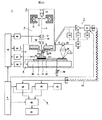
1つの実施例における回路パターン検査装置1の構成を図1に示す。回路パターン検査装置1は、室内が真空排気される検査室2と、検査室2内に試料基板9を搬送するための予備室(本実施例では図示せず)を備えており、この予備室は検査室2とは独立して真空排気できるように構成されている。また、回路パターン検査装置1は上記検査室2と予備室の他に制御部6、画像処理部5から構成されている。検査室2内は大別して、電子光学系3、二次電子検出部7、試料室8、光学顕微鏡部4から構成されている。電子光学系3は、電子銃10、電子線引き出し電極11、コンデンサレンズ12、ブランキング用偏向器13、走査偏向器15、絞り14、対物レンズ16、反射板17、ExB偏向器18から構成されている。二次電子検出部7のうち、二次電子検出器20が検査室2内の対物レンズ16の上方に配置されている。二次電子検出器20の出力信号は、検査室2の外に設置されたプリアンプ21で増幅され、AD変換機22によりデジタルデータとなる。試料室8は、試料台30、Xステージ31、Yステージ32、位置モニタ用測長器33、被検査基板高さ測定器34から構成されている。光学顕微鏡部4は、検査室2の室内における電子光学系3の近傍であって、互いに影響を及ぼさない程度離れた位置に設備されており、電子光学系3と光学顕微鏡部4の間の距離は既知である。そして、Xステージ31またはYステージ32が電子光学系3と光学顕微鏡部4の間において既知の距離を往復移動するようになっている。光学顕微鏡部4は光源35、光学レンズ36、CCDカメラ37により構成されている。光源35、CCDカメラ37等は、真空排気された検査室2の外部に設置する構成でもよい。画像処理部5は、第一画像記憶部38、第二画像記憶部39、比較演算部40、欠陥判定処理部41より構成されている。モニタ42により、画像記憶部38および39に取り込まれた電子線画像と、リアルタイムでワーク用メモリ内に取得された電子線画像とCCDカメラ37にて撮像された光学画像、そして比較演算部40で比較処理された後の差画像を任意に選択して表示することができる。装置各部の動作命令および動作条件は、制御部6から入出力される。制御部6には、あらかじめ電子線発生時の加速電圧、電子線偏向幅、偏向速度、二次電子検出装置の信号取り込みタイミング、試料台移動速度等々の条件が、目的に応じて任意にあるいは選択して設定できるよう入力されている。制御部6は、補正制御回路43を用いて、位置モニタ用測長器33、被検査基板高さ測定器34の信号から位置や高さのずれをモニタし、その結果より補正信号を生成し、電子線が常に正しい位置に照射されるよう対物レンズ電源45や走査偏向器44に補正信号を送る。
Hereinafter, an example of an inspection method and an apparatus according to an embodiment of the present invention will be described in detail with reference to the drawings.
FIG. 1 shows a configuration of a circuit
被検査基板9の画像を取得するためには、細く絞った電子線19を該被検査基板9に照射し、二次電子46を発生させ、これらを電子線19の走査およびX−Yステージ31、32の移動と同期して検出することで該被検査基板9表面の電子線画像を得る。本実施例の回路パターン検査装置では、通常SEMに比べ約100倍以上の、例えば100nAの大電流電子線を一回のみ走査する信号を検出することにより電子線画像を形成する構成とした。走査幅は100μmとし、1画素は0.1μm2とし、1回の走査を1μsで行うようにした。
In order to obtain an image of the
電子銃10には拡散補給型の熱電界放出電子源が使用されている。この電子銃10を用いることにより、従来の例えばタングステン(W)フィラメント電子源や、冷電界放出型電子源に比べて安定した電子線電流を確保することができるため、明るさ変動の少ない電子線画像が得られる上、電子線電流を大きく設定することができるため、一回の走査で高S/Nの電子線画像を形成し高速検査を実現することができる。電子線19は、電子銃10と引き出し電極11との間に電圧を印加することで電子銃10から引き出される。電子線19の加速は、電子銃10に高電圧の負の電位を印加することでなされる。これにより、電子線19はその電位に相当するエネルギーで試料台30の方向に進み、コンデンサレンズ12で収束され、さらに対物レンズ16により細く絞られて試料台30上のX−Yステージ31、32の上に搭載された被検査基板9(半導体ウエハ、チップあるいは液晶、マスク等微細回路パターンを有する基板)に照射される。なお、ブランキング用偏向器13には、走査信号およびブランキング信号を発生する信号発生器44が接続され、コンデンサレンズ12および対物レンズ16には、各々レンズ電源45が接続されている。被検査基板9には、高圧電源48により負の電圧を印加できるようになっている。この高圧電源48の電圧を調節することにより一次電子線を減速し、電子銃10の電位を変えずに被検査基板9への電子線照射エネルギーを最適な値に調節することができる。
The
被検査基板9上に電子線19を照射することによって発生した二次電子46は、基板9に印加された負の電圧により加速される。被検査基板9上方に、ExB偏向器18が配置されており、これにより加速された二次電子46は所定の方向へ偏向される。ExB偏向器18にかける電圧と磁界の強度により、偏向量を調整することができる。また、この電磁界は、試料に印加した負の電圧に連動させて可変させることができる。ExB偏向器18により偏向された二次電子46は、所定の条件で反射板17に衝突する。この反射板17に加速された二次電子46が衝突すると、反射板17からは数V〜50eVのエネルギーを持つ第二の二次電子47が発生する。
二次電子検出部7は、真空排気された検査室2内には二次電子検出器20が、検査室2の外にはプリアンプ21、AD変換器22、光変換手段23、伝送手段24、電気変換手段25、高圧電源26、プリアンプ駆動電源27、AD変換器駆動電源28、逆バイアス電源29から構成されている。既に記述したように、二次電子検出部7のうち、二次電子検出器20が検査室2内の対物レンズ16の上方に配置されている。二次電子検出器20、プリアンプ21、AD変換器22、光変換手段23、プリアンプ駆動電源27、AD変換器駆動電源28は、高圧電源26により正の電位にフローティングしている。上記反射板17に衝突して発生した第二の二次電子47は、この吸引電界により検出器20へ導かれる。二次電子検出器20は、電子線19が被検査基板9に照射されている間に発生した二次電子46がその後加速されて反射板17に衝突して発生した第二の二次電子47を、電子線19の走査のタイミングと連動して検出するように構成されている。二次電子検出器20の出力信号は、検査室2の外に設置されたプリアンプ21で増幅され、AD変換器22によりデジタルデータとなる。AD変換器22は、半導体検出器20が検出したアナログ信号をプリアンプ21によって増幅された後に直ちにデジタル信号に変換して、画像処理部5に伝送するように構成されている。検出したアナログ信号を検出直後にデジタル化してから伝送するので、従来の装置よりも高速で且つS/N比の高い信号を得ることができる。
The
X−Yステージ31、32上には被検査基板9が搭載されており、検査実行時にはX−Yステージ31、32を静止させて電子線19を二次元に走査する方法と、検査実行時にX−Yステージ31、32をY方向に連続して一定速度で移動されるようにして電子線19をX方向に直線に走査する方法のいずれかを選択できる。ある特定の比較的小さい領域を検査する場合には前者のステージを静止させて検査する方法、比較的広い領域を検査するときは、ステージを連続的に一定速度で移動して検査する方法が有効である。なお、電子線19をブランキングする必要がある時には、ブランキング用偏向器13により電子線19が偏向されて、電子線が絞り14を通過しないように制御できる。これにより、検査に必要でない電子線を試料に照射しないように制御し、被検査基板9の帯電を抑制することができる。
The
位置モニタ用測長器33として、本実施例ではレーザ干渉による測長計を用いた。Xステージ31およびYステージ32の位置が実時間でモニタでき、制御部6に転送されるようになっている。また、Xステージ31、Yステージ32の各種データも同様に各々のドライバから制御部6に転送されるように構成されている。制御部6はこれらのデータに基いて電子線19が照射されている領域や位置が正確に把握できるようになっており、必要に応じて実時間で電子線19の照射位置の位置ずれを補正制御回路43より補正するようになっている。また、被検査基板毎に、電子線を照射した領域を記憶できるようになっている。
In this embodiment, a length measuring device based on laser interference was used as the position monitor
光学式高さ測定器34は、電子ビーム以外の測定方式である光学式測定器、例えばレーザ干渉測定器や反射光の位置で変化を測定する反射光式測定器が使用されており、X−Yステージ上31、32に搭載された被検査基板9の高さを実時間で測定するように構成されている。本実施例では、スリットを通過した細長い白色光を透明な窓越しに該被検査基板9に照射し、反射光の位置を位置検出モニタにて検出し、位置の変動から高さの変化量を算出する方式を用いた。この光学式高さ測定器34の測定データに基いて、電子線19を細く絞るための対物レンズ16の焦点距離がダイナミックに補正され、常に非検査領域に焦点が合った電子線19を照射できるようになっている。また、被検査基板9の反りや高さ歪みを電子線照射前に予め測定しており、そのデータをもとに対物レンズ16の検査領域毎の補正条件を設定するように構成することも可能である。
As the optical
画像処理部5は第一画像記憶部38と第二画像記憶部39、比較演算部40、欠陥判定処理部41、モニタ42により構成されている。上記二次電子検出器20で検出された被検査基板9の画像信号は、プリアンプ21で増幅され、AD変換器22でデジタル化された後に光変換器23で光信号に変換され、光ファイバ24によって伝送され、電気変換器25にて再び電気信号に変換された後に、制御部6からの命令により第一画像記憶部38あるいは第二記憶部39に記憶される。比較演算部40には、制御部6からの命令によりこれらの二つの記憶装置に記憶された画像信号が送られ、各々位置合せ、信号レベルの規格化、ノイズ信号を除去するための各種画像処理を施し、双方の画像信号を比較演算する。欠陥判定処理部41は、比較演算部40にて比較演算された差画像信号の絶対値を所定のしきい値と比較し、所定のしきい値よりも差画像信号レベルが大きい場合にその画素を欠陥候補と判定する。モニタ42は、制御部6からの指示により、検査途中に実時間で欠陥判定処理部41が欠陥と判定した箇所の位置や欠陥検出総数等を表示したり、第一あるいは第二記憶部38・39に記憶された画像データを表示したりする。
The
これまで回路パターン検査装置1の全体の構成について説明してきたが、次に被検査回路パターンの製造プロセスと、発生する欠陥の内容について説明する。本実施例では、半導体ウエハを例に取り説明する。図2は半導体装置の製造プロセスを示している。図2(a)に示すように、半導体装置は多数のパターン形成を繰り返している。パターン形成工程は、おおまかに、成膜、感光ホトレジスト塗布、感光、現像、エッチング、レジスト除去、洗浄の各ステップにより構成されている。また、図2(b)に示すように、さらに埋め込み成膜、表面研磨、洗浄という工程が加わる場合もある。図2(b)は、主に孔形成工程や配線形成工程で採用されているプロセスである。この各ステップにおいて、加工のための製造条件が最適化されていないと、基板ウエハ上に半導体装置の回路パターンが正常に形成されず、正常に動作しない不良品となる。製造工程途中の不良発生を早期に検知し、異常の内容を把握し、製造条件を最適化するために、各工程で高精度に検査を実施しする必要がある。図2(a)および図2(b)に検査を実施する工程の一例を示す。図3(a)、(b)および図4(a)、(b)に製造過程における半導体ウエハ上に形成された回路パターンの概略と発生する不良の内容を示す。図3(a)は正常に加工された回路パターンの平面図、図3(b)は不良が発生した回路パターンの平面図である。例えば図2の成膜工過程で異常が発生すると、パーティクルが発生し、表面に付着し図3(b)中の孤立欠陥等になる。また、感光時の露光条件、例えば焦点や露光時間が最適でないと、図3(b)中のショートや断線、パターン細りとなる。感光時のマスクやレチクルに欠陥が存在すると、感光単位であるショット毎にショット内の同一箇所に同様のパターン異常が発生する。また、エッチング条件が最適でないと、孔パターンの導通不良が発生したりパターン寸法が設計値とおりに形成されない。また、エッチング条件が最適でないとパーティクルを発生し、このパーティクルによりエッチングされない箇所が発生し、パターンショートや孤立欠陥となる。洗浄過程では、洗浄層の液の汚れや剥離した薄膜や異物の再付着によりパーティクルがウエハ表面に付着したり、洗浄あるいは乾燥時の水切れ条件により局所的に酸化膜を発生したり膜厚のムラを発生しやすい。さらに、埋め込み研磨過程では、研磨剤が残存したり研磨によるキズを発生しやすい。このように、一つの工程で発生する欠陥について図3に示したが、図4(a)、(b)は半導体装置を製造していく工程全体で発生し得る不良を断面図で示したものである。図4(a)は正常に形成された回路パターンの断面の模式図であり、図4(b)は不良が発生した回路パターンの断面模式図である。トランジスタを形成する上で必要な素子分離工程では、基板とトランジスタが接触していること、トランジスタは各々分離されていて接合部によりゲート電極や配線からの信号で電流が流れることが必要であるが、トランジスタと基板をつなぐ孔パターンが導通不良となったり配線同士がショートしたり、トランジスタ同士がショート欠陥によりつながってしまうと正常に動作しなくなる。
The overall configuration of the circuit
このように、半導体装置の各製造工程は、図2、図3および図4に示したようにさまざまな材料の層が存在し、且つ段差や形状も様々である。このような被検査回路パターンに図1で説明した検査装置1で検査した場合の作用について説明すると、一次電子線19は、固体に入射すると内部に進入しながらそれぞれの深さにおいて殻内電子を励起してエネルギーを失っていく。また、それととにも一次電子線が後方に散乱された反射電子が、やはり固体内で電子を励起させながら表面へ向かって進む現象が生ずる。これら複数の過程を経て、殻内電子は固体表面から表面障壁を超えて二次電子となって数V〜50eVのエネルギーを持って真空中へ出る。一次電子線と固体表面のなす角度が浅いほど、一次電子線の進入距離とその位置から固体表面までの距離との比が小さくなり、二次電子が表面から放出されやすくなる。したがって、二次電子の発生は一次電子線と固体表面の角度に依存しており、二次電子発生量が試料表面の凹凸や材料を示す情報となる。また、材料により二次電子発生の効率が異なるので、コントラストに大きく影響する。
Thus, in each manufacturing process of the semiconductor device, as shown in FIGS. 2, 3, and 4, layers of various materials exist, and steps and shapes are also various. The operation when such a circuit pattern to be inspected is inspected by the
電子線画像のコントラストは、試料に照射した電子線により発生し検出される二次電子の量により形成される。以下に電子線画像のコントラストに影響する照射条件について述べる。図5(a)と図5(b)は、電子線照射エネルギーがコントラストへの影響を示すグラフであり、図5(a)は照射エネルギーが適切な場合を示し図5(b)は照射条件が不適切な場合を示している。また、縦軸は画像の明るさと相関が大である帯電の程度、横軸には電子線の照射時間である。実線Aは、試料にホトレジストを用いた場合、点線Bは試料に配線材料を用いた場合である。 The contrast of the electron beam image is formed by the amount of secondary electrons generated and detected by the electron beam irradiated on the sample. The irradiation conditions which affect the contrast of the electron beam image will be described below. 5 (a) and 5 (b) are graphs showing the effect of the electron beam irradiation energy on the contrast. FIG. 5 (a) shows the case where the irradiation energy is appropriate, and FIG. 5 (b) shows the irradiation condition. Indicates an inappropriate case. The vertical axis represents the degree of charging that has a large correlation with the brightness of the image, and the horizontal axis represents the irradiation time of the electron beam. The solid line A indicates the case where photoresist was used for the sample, and the dotted line B indicates the case where wiring material was used for the sample.
図5(a)より、照射時間が少ない時間領域Cでは各材料の明るさ変動が少なく、照射時間が比較的多くなってくる時間領域Dだと照射時間による明るさの変化が大きくなり、最終的に照射時間が多い時間領域Eでは再び照射時間による明るさ変動が少なくなる。また、図5(b)より、照射条件が適切でない場合には、照射時間が少ない時間領域Cにおいても、照射時間に対する明るさ変動が大きく、安定した画像を得るのが困難である。従って、この材料で高速に且つ安定した電子線画像を取得するためには図5(a)の照射条件にて画像を取得する必要がある。 As shown in FIG. 5 (a), in the time region C where the irradiation time is short, the change in brightness of each material is small, and in the time region D where the irradiation time is relatively long, the change in brightness due to the irradiation time is large. In the time region E where the irradiation time is long, the brightness variation due to the irradiation time is reduced again. Further, from FIG. 5B, when the irradiation conditions are not appropriate, even in the time region C where the irradiation time is short, the brightness varies greatly with respect to the irradiation time, and it is difficult to obtain a stable image. Therefore, in order to acquire a high-speed and stable electron beam image using this material, it is necessary to acquire an image under the irradiation conditions shown in FIG.
本実施例の検査装置1は、電子線を照射した直後に二次電子信号を検出して電子線画像を形成するため、上記図5における時間領域Cの信号差が検査時の回路パターンと下地のコントラストとなる。上記電子線の試料への照射条件としては、電子線電流値、電子線の走査速度、試料に照射する電子線の照射エネルギー、同一箇所に対する電子線の照射回数が挙げられる。これらのうち、電子線の走査速度および照射回数を増加すると検査時間が長くなってしまう。また、電子線電流値を所定のS/Nよりも小さくすると、電子線画像から欠陥の有無を画像処理で自動検出することが困難となる。そのため、本実施例では、これらパラメータのうち試料に照射する電子線の照射エネルギーを自由に調整制御し帯電の状態を変えることにより、コントラストを調整する方法で条件を設定した。試料への電子線照射エネルギーを調整するために、試料である半導体ウエハ9に高圧電源48により一次電子を減速するための負の電圧を印加し、この電圧を調整することにより電子線19の照射エネルギーを適宜調整できるように構成している。これにより、電子銃10に印加する加速電圧を変化させる場合には電子線19の軸変化が発生し各種調整が必要になるのに対し、本実施例ではそのような調整を行わずに同様の効果を得ることができる。そのため、発明者は、上記試料である半導体ウエハ9に印加する負の電圧を調整することにより、時間領域Cのコントラストが大きくなるような電子線の照射エネルギーを、各種半導体回路パターンについて評価し、最適な条件を求めた。
Since the
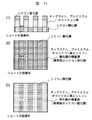
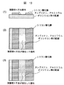
図6に、被検査回路パターンの材料および段差による電子線照射エネルギーの条件一覧と、検出したい欠陥の種類による電子線照射エネルギーの条件一覧を示す。本実施例では、検査装置1の電子線の加速電圧を10kVとした。図6において、被検査半導体ウエハの情報、すなわちパターン形成工程、段差、検出したい欠陥の種類について、分類、内容、材料等、適切な照射エネルギー範囲、照射エネルギー最適値を示す。従って、例えば試料および試料台に印加する負の電圧を−9kVに設定すると、試料へ照射される電子線のエネルギーは1kVということになる。例えば、孔形成工程においては、下地のトランジスタあるいは配線と上層のトランジスタあるいは配線をつなぐために形成するので、例えばシリコン酸化膜を形成し、所望の箇所に孔パターンをホトレジストパターンで形成し、それをマスクにエッチングし、下層との導通をとり、レジストを除去した後に導電材料を充填し、表面を研磨して平坦化する製造方法の場合、ホトレジスト現像後(図7(1)参照)では最表面はホトレジスト、下地はシリコン酸化膜という組み合わせになる。この場合に、500V以下の照射エネルギーで電子線を照射すると、両方の材料とも絶縁材料であるために同様の暗いコントラストとなり、パターン形状が認識できず、欠陥の検出が困難となる(図7(2)参照)。そのため、帯電しやすい条件として照射エネルギー3kVとなるように電子線を照射すると、ホトレジストは明るく、シリコン酸化膜はそれと比較して暗くなるため、コントラストがつき、欠陥の検出が容易となる(図7(3))。別の例では、孔形成工程エッチング後の場合(図8(1)参照)には、最表面がシリコン酸化膜であり、下地に導電物、例えばタングステンやポリシリコン等という組み合わせになる。しかし、孔径が小さく、孔の深さが深い場合には、500V以下の照射エネルギーで電子線を照射すると孔底部まで電子線が到達し二次電子を発生するに至らない(図8(2))。このような場合、孔底部まで電子線を到達し二次電子信号を得るためには1kV以上の照射エネルギー、望ましくは3kV程度の照射エネルギーに設定する必要がある(図8(3))。さらに別の例では、孔形成工程で、孔を形成した後に穴内部に導電物を充填し表面を平坦化した工程の場合(図9(1))、充填された導電物と下層のトランジスタあるいは配線が導電しているので、材料の組み合わせは導電物と絶縁物ということになる。また、表面が平坦であるので、特に電子線の照射エネルギーを高くしなくても各々の箇所に電子線を照射することができる。そのため、電子線の照射条件としては300V以上であれば問題ない。通常このような工程では、孔に充填された導電物と下層のトランジスタあるいは配線が導通しているかどうかが問題となる。このような場合には、電位コントラストを強調できる低照射エネルギーの条件が望ましい。3kV以下、望ましくは1kV以下に設定することにより高感度に導通不良を検出することができる(図9(2))。このような試料で例えば5kV以上の照射エネルギーに設定すると、孔パターンの形状は見えるが導通不良等の欠陥は正常部とコントラスト差がなくなり、欠陥として検出できなくなる(図9(3))。
FIG. 6 shows a list of conditions of the electron beam irradiation energy according to the material and step of the circuit pattern to be inspected, and a list of conditions of the electron beam irradiation energy according to the type of defect to be detected. In the present embodiment, the acceleration voltage of the electron beam of the
次は、配線を形成する工程のコントラストについて説明する。図6に示したように、配線の材料は導電材料、例えばアルミニウムやタングステン等の金属やポリシリコン等の準金属が用いられ、下地にはシリコン酸化膜等絶縁材料が存在する場合が多い(図10(1))。このような場合には、下地が絶縁材料、表面が導電材料なので、電子線の照射エネルギーは低くても高くてもコントラストを得ることができる。図10(2)は500V〜1kVの照射エネルギーで取得した画像の例であり、図10(3)は3kV〜5kVで取得した画像の例である。しかし、検出したい欠陥が段差の大きい配線の底部に存在するショートのような欠陥の場合には、図10(3)に示したように、比較的高い照射条件が望ましい。また、別の配線の例では、配線材料の表面がシリコン窒化膜やチタン窒化膜のような絶縁材料に近い材料で覆われている場合には、例えば図11(1)の場合には電子線が照射されるのはシリコン窒化膜とシリコン酸化膜という組み合わせになる。このような場合には、電子線の照射エネルギーが低いとコントラストがつかない。図11(2)に500V〜1kVの照射エネルギーで電子線を照射した場合の画像を示す。従って、図11(1)の試料を検査する場合には、1kV以上、望ましくは3kV以上の照射エネルギーに設定することにより、シリコン窒化膜とシリコン酸化膜のコントラストを得ることができ、欠陥を検出しやすくなる。図11(3)に照射エネルギー3kVの場合の電子線画像を示す。さらに、配線形成過程で、最初に絶縁材料であるシリコン酸化膜をエッチングで削り、その上に配線材料を充填し表面を研磨する製造プロセス(図12(1))においては、段差が無いので照射エネルギーを高くする必要が無い。このプロセスにおいては、下地の配線との導通がとれているか、配線材料がシリコン酸化膜の段差底部まで充填されているかが問題となるので、孔形成工程の場合と同様に、比較的照射エネルギーが低いほうが導通不良を検出しやすい。図12(2)は、照射エネルギーが比較的低い1kVの場合の電子線画像、図12(3)は照射エネルギーが比較的高い場合の電子線画像を示す。いずれの画像も欠陥部は認識可能であるが、下地とのコントラスト差が大きい方が画像比較で欠陥部を抽出しやすいので、低い照射エネルギーの方が有利であることがわかる。 Next, the contrast in the step of forming the wiring will be described. As shown in FIG. 6, a conductive material, for example, a metal such as aluminum or tungsten, or a quasi-metal such as polysilicon is used as a material of the wiring, and an insulating material such as a silicon oxide film is often provided as a base (see FIG. 6). 10 (1)). In such a case, since the base is an insulating material and the surface is a conductive material, contrast can be obtained regardless of whether the irradiation energy of the electron beam is low or high. FIG. 10 (2) is an example of an image obtained at an irradiation energy of 500 V to 1 kV, and FIG. 10 (3) is an example of an image obtained at 3 kV to 5 kV. However, when the defect to be detected is a defect such as a short-circuit existing at the bottom of the wiring having a large step, a relatively high irradiation condition is desirable as shown in FIG. In another wiring example, when the surface of the wiring material is covered with a material close to an insulating material such as a silicon nitride film or a titanium nitride film, for example, in the case of FIG. Is irradiated in a combination of a silicon nitride film and a silicon oxide film. In such a case, if the irradiation energy of the electron beam is low, the contrast cannot be obtained. FIG. 11B shows an image when the electron beam is irradiated at an irradiation energy of 500 V to 1 kV. Therefore, when inspecting the sample of FIG. 11A, the contrast between the silicon nitride film and the silicon oxide film can be obtained by setting the irradiation energy to 1 kV or more, preferably 3 kV or more, and the defect can be detected. Easier to do. FIG. 11 (3) shows an electron beam image when the irradiation energy is 3 kV. Further, in the manufacturing process (FIG. 12 (1)) in which a silicon oxide film, which is an insulating material, is first etched away in a wiring forming process, a wiring material is filled thereon, and the surface is polished (FIG. 12A). There is no need to increase energy. In this process, there is a problem whether conduction is established with the underlying wiring or the wiring material is filled up to the bottom of the step of the silicon oxide film. Therefore, similarly to the case of the hole forming step, the irradiation energy is relatively high. The lower the value, the easier it is to detect conduction failure. FIG. 12 (2) shows an electron beam image when the irradiation energy is relatively low at 1 kV, and FIG. 12 (3) shows an electron beam image when the irradiation energy is relatively high. In any of the images, the defective portion is recognizable. However, it can be understood that a lower irradiation energy is more advantageous because a larger difference in contrast from the base makes it easier to extract the defective portion by image comparison.
次に、洗浄等による薄膜残りを検出する場合(図13(1))について説明する。
図13(2)は電子線の照射エネルギーを500V〜800Vで照射した場合の電子線画像、図13(3)は照射エネルギーを5kVに設定した場合の電子線画像を示す。例えば照射エネルギーを5kVに設定すると、電子線はほとんど薄膜を突き抜けてしまうので、薄膜有無の情報が画像として得られない(図13(3))。従って、比較的低い照射エネルギーで電子線を照射すると、薄膜部が他の領域よりも帯電し、コントラストがつくようになるので検出しやすくなる(図13(2))。
Next, a case of detecting a thin film residue due to washing or the like (FIG. 13A) will be described.
FIG. 13B shows an electron beam image when the irradiation energy of the electron beam is 500 V to 800 V, and FIG. 13C shows an electron beam image when the irradiation energy is set to 5 kV. For example, if the irradiation energy is set to 5 kV, the electron beam hardly penetrates the thin film, so that information on the presence or absence of the thin film cannot be obtained as an image (FIG. 13 (3)). Therefore, when the electron beam is irradiated with a relatively low irradiation energy, the thin film portion is charged more than other regions and a contrast is obtained, so that the detection becomes easy (FIG. 13 (2)).
これまでで述べてきたコントラストの特性を評価した一例について、以下に記載する。試料および試料台に印加する負の電圧を変えることにより電子線照射エネルギーを変えて各試料におけるコントラストの変化を調べた。ここで、コントラストとは画像の明るさ平均に対するパターン部の明るさと下地部の明るさの差の絶対値の割合を示しており、コントラストC(%)=|(パターン部の明るさ)−(下地部の明るさ)|/(画像の明るさ平均)という式で表される。本評価は、電子ビーム電流は50〜100nA、電子線照射回数1回(加算無し)、ビーム偏向器は50〜100μm、画像取得時の画素サイズは0.05〜0.1μm、信号検出速度は100MHzすなわち10nA/画素、電子ビーム径は0.1〜0.2μm、電子線の初期加速電圧は10kVという条件で電子線画像を取得して実施した。 An example of evaluating the contrast characteristics described above will be described below. The change in contrast in each sample was examined by changing the electron beam irradiation energy by changing the negative voltage applied to the sample and the sample stage. Here, the contrast indicates the ratio of the absolute value of the difference between the brightness of the pattern portion and the brightness of the base portion with respect to the average brightness of the image, and the contrast C (%) = | (the brightness of the pattern portion) − ( This is expressed by the following formula: brightness of base portion) / (average brightness of image). In this evaluation, the electron beam current was 50 to 100 nA, the number of times of electron beam irradiation was 1 (no addition), the beam deflector was 50 to 100 μm, the pixel size at the time of image acquisition was 0.05 to 0.1 μm, and the signal detection speed was An electron beam image was acquired under the conditions of 100 MHz, that is, 10 nA / pixel, the electron beam diameter was 0.1 to 0.2 μm, and the initial acceleration voltage of the electron beam was 10 kV.
第一の例として、表面の材質がシリコン窒化膜で、下地がシリコン酸化膜とシリコンで形成されているライン形状の回路パターンAについてコントラスト特性を評価した。本回路パターンAでは、パターン部の段差は約0.15μmであった。回路パターンAのコントラスト特性を図14に示す。下地がシリコンの部分においては、電子線照射エネルギーが低いほうがパターン部と下地のコントラストが高くなる。しかし、下地がシリコン酸化膜の部分においては、リターディング電圧が7〜8kV近辺すなわち照射エネルギーが2〜3kVでコントラストが高くなった。欠陥が発生する箇所は、下地がシリコンの箇所かシリコン酸化膜の箇所かを特定できない。そのため、回路パターンAを検査する場合には、下地がシリコンの場合でもシリコン酸化膜の場合でもコントラストが高い条件が適している。従って、シリコン窒化膜とシリコン酸化膜の組み合わせを有し、段差が1.5μm程度である回路パターンAにおいてはリターディング電圧が7〜8kV近辺すなわち照射エネルギーが2〜3kVの条件が検査時の最適値となる。 As a first example, the contrast characteristics of a line-shaped circuit pattern A in which the surface material is a silicon nitride film and the base is formed of a silicon oxide film and silicon were evaluated. In the circuit pattern A, the step in the pattern portion was about 0.15 μm. FIG. 14 shows the contrast characteristics of the circuit pattern A. In a silicon base, the lower the electron beam irradiation energy, the higher the contrast between the pattern portion and the base. However, in the portion where the underlayer was a silicon oxide film, the contrast was high when the retarding voltage was around 7 to 8 kV, that is, the irradiation energy was 2 to 3 kV. The location where the defect occurs cannot be specified whether the base is a silicon location or a silicon oxide film location. Therefore, when inspecting the circuit pattern A, a condition with high contrast is suitable regardless of whether the underlying layer is silicon or a silicon oxide film. Therefore, in a circuit pattern A having a combination of a silicon nitride film and a silicon oxide film and having a level difference of about 1.5 μm, the condition where the retarding voltage is around 7 to 8 kV, that is, the irradiation energy is 2 to 3 kV is optimal for the inspection. Value.
第二の例は、穴パターンに導電性材料を埋め込み、表面を平坦に研磨した回路パターンBについてコントラスト特性を評価した例である。穴周囲の材料はシリコン酸化膜であり、穴内部の導電材料はイオンをドープしたポリシリコンの場合とタングステンの場合がある。いずれも特性は類似しているが、本例はイオンをドープしたポリシリコンを用いた場合である。表面を平坦に研磨しているので、段差はほとんどない。この回路パターンBのコントラスト特性を図15に示す。リターディング電圧が高いほど、すなわち電子線照射エネルギーが低いほど穴周辺部のシリコン酸化膜部と穴内部のポリシリコン部のコントラストが高くなった。照射エネルギーが高くなると、コントラストはほとんど0%となり、画像上で穴パターンと周囲を見分けることが困難となり、その結果、欠陥検査が困難となる。従って、表面が平坦で、導電物と絶縁材料の組み合わせである回路パターンBにおいては、電子線照射エネルギーが500V以下の条件が検査時の最適値となる。電位コントラスト欠陥検査には低照射エネルギーが有利である。 The second example is an example in which a conductive material is embedded in a hole pattern and the contrast characteristics of a circuit pattern B whose surface is polished flat are evaluated. The material around the hole is a silicon oxide film, and the conductive material inside the hole may be ion-doped polysilicon or tungsten. Although the characteristics are similar in both cases, this example is a case where polysilicon doped with ions is used. Since the surface is polished flat, there is almost no step. FIG. 15 shows the contrast characteristics of the circuit pattern B. The higher the retarding voltage, that is, the lower the electron beam irradiation energy, the higher the contrast between the silicon oxide film portion around the hole and the polysilicon portion inside the hole. When the irradiation energy increases, the contrast becomes almost 0%, and it becomes difficult to distinguish the hole pattern from the surroundings on the image, and as a result, it becomes difficult to perform a defect inspection. Therefore, in the case of the circuit pattern B having a flat surface and a combination of a conductive material and an insulating material, the condition where the electron beam irradiation energy is 500 V or less is the optimum value at the time of inspection. Low irradiation energy is advantageous for potential contrast defect inspection.
第三の例は、表面が導電性ポリシリコンで形成された島状に各々独立したトランジスタパターンと、下地がシリコン酸化膜である回路パターンCについてコントラスト特性を評価した例である。この回路パターンCの孤立パターン部は下地に対して段差が1μm程度である。この回路パターンCのコントラスト特性を図16に示す。本回路パターンCでは、リターディング電圧が低くなると、すなわち照射エネルギーが高くなるとコントラストが高くなった。照射エネルギー1kV以上でコントラストは25%以上となり、さらに照射エネルギーが3kV以上の場合には照射エネルギーは30%以上となった。従って、段差の大きいパターンCにおいては、照射エネルギー3kV以上の条件が検査時の最適値となる。高段差パターン検査には高照射エネルギーが有利である。 The third example is an example in which the contrast characteristics are evaluated for an independent transistor pattern in the form of an island whose surface is formed of conductive polysilicon and a circuit pattern C whose underlying layer is a silicon oxide film. The isolated pattern portion of the circuit pattern C has a step of about 1 μm with respect to the base. FIG. 16 shows the contrast characteristics of the circuit pattern C. In the present circuit pattern C, the contrast increased as the retarding voltage decreased, that is, as the irradiation energy increased. When the irradiation energy was 1 kV or more, the contrast was 25% or more, and when the irradiation energy was 3 kV or more, the irradiation energy was 30% or more. Therefore, in the pattern C having a large step, the condition of the irradiation energy of 3 kV or more becomes the optimum value at the time of inspection. High irradiation energy is advantageous for high step pattern inspection.
以上、一例を述べて説明してきたが、図6に示すように、段差が大きい場合には照射エネルギーは高く(1kV以上)、段差が低いあるいは無い場合には照射エネルギーを低く(3kV以下)設定する。また、導電材料と絶縁材料の組み合わせでは、照射エネルギーは低くても高くてもコントラストを得ることができるが、絶縁材料と絶縁材料の組み合わせでは、1kV以上に設定し、材料による帯電状態の差によりコントラストを得る。さらに形状欠陥を検出したい場合には500V以上、望ましくは1kV以上の照射エネルギーで、電位コントラスト欠陥すなわち導通不良やショート等の電気的な欠陥を検出したい場合には、3kV以下、望ましくは1kV以下の照射エネルギーに設定する必要がある。これらの条件を、検査装置1の検査条件データベースに予め入力し、段差や材料の条件を入力することにより検査に適した照射エネルギーを検索できるようにした。
As described above, an example has been described. As shown in FIG. 6, when the step is large, the irradiation energy is set high (1 kV or more), and when the step is low or no, the irradiation energy is set low (3 kV or less). I do. Further, in the case of a combination of a conductive material and an insulating material, contrast can be obtained regardless of whether the irradiation energy is low or high. Get contrast. Furthermore, when it is desired to detect a shape defect, irradiation energy of 500 V or more, preferably 1 kV or more, and when it is desired to detect a potential contrast defect, that is, an electrical defect such as conduction failure or short circuit, 3 kV or less, preferably 1 kV or less. It is necessary to set the irradiation energy. These conditions are input in advance to the inspection condition database of the
このように、操作画面上で、被検査回路パターンの状態を示す項目を特定してこれに応じた電子線画像のコントラストを確認して電子線電圧を含む電子線照射条件を求めて記憶し、被検査回路パターンの状態を操作画面に表示し、該表示した画面について記憶した電子線照射条件を使用して電子線照射条件を確定し、以って該電子線照射条件で電子線を前記被検査回路パターンに1回照射走査して電子線画像を形成し、検査を実施することを特徴とする回路パターンの検査方法および操作画面上で、被検査回路パターンの状態を示す項目を特定してこれに応じた電子線画像のコントラストを確認して電子線電圧を含む電子線照射条件を求めて記憶し、被検査回路パターンの状態を被検査回路パターンの材料または段差、および検出したい欠陥の種類について操作画面に表示し、該表示した画面について記憶した電子線照射条件を使用して電子線照射条件を確定実施することを特徴とする回路パターンの検査方法が提供される。 In this manner, on the operation screen, the item indicating the state of the circuit pattern to be inspected is specified, the contrast of the electron beam image corresponding thereto is checked, and the electron beam irradiation condition including the electron beam voltage is obtained and stored, The state of the circuit pattern to be inspected is displayed on the operation screen, the electron beam irradiation conditions are determined using the electron beam irradiation conditions stored for the displayed screen, and the electron beam is irradiated under the electron beam irradiation conditions. The inspection circuit pattern is irradiated once to form an electron beam image, and the inspection is performed. In the inspection method and the operation screen of the circuit pattern, an item indicating the state of the circuit pattern to be inspected is specified. The contrast of the electron beam image corresponding to this is checked, the electron beam irradiation conditions including the electron beam voltage are obtained and stored, and the state of the circuit pattern to be inspected is determined by the material or step of the circuit pattern to be inspected and the defect to be detected. For displaying the operation screen type, method of inspecting a circuit pattern, characterized by determining implementing electron beam irradiation conditions using the stored electron beam irradiation conditions for the display the screen is provided.
次に、これまで述べてきた電子線照射エネルギーの条件を用いて実際に検査を実行するフローについて説明する。図17に検査条件設定のフローを示す。操作画面上で検査条件(以下レシピと称する)を作成するモードを選択する。そしてウエハを実際に検査装置内にロードする。既にレシピを作成している場合に、以前のレシピを編集修正して新たなレシピとするか、まったく新規にレシピを作成するかを選択する。そして、電子線を照射した画像を取得する前に、電子線照射条件を選択する。詳細は、図17を参照することによって容易に理解できよう。ここで、図18に示すいくつかの選択項目の中から電子線照射エネルギーを選択する。選択方法の一つは、電子線の照射エネルギーを数段階準備しておき、その段階値を直接選択・入力するものである。例えば図18(1)の例では、低照射エネルギーモード、中照射エネルギーモード、高照射エネルギーモードの3段階から選択する。図18(2)の例では、設定可能な照射エネルギーの数値を選択する。図18(3)の例では、照射エネルギーを数値で入力する。もう一つの選択方法を図19に示す。この方法では、材料や形状のパラメータを選択することにより、適切な照射エネルギーの範囲を設定するというものである。図19(1)に示した例では形状欠陥検査モードと電位コントラスト欠陥検査モードとその中間すなわち両方に対応できるモードの3つの中から選択するというものである。図19(2)に示した例では、導電材料/絶縁材料、導電材料/導電材料、絶縁材料/絶縁材料の中から検査モードを選択するというものである。さらに図19(3)に示した例では、高段差・中段差・低段差(段差なし)の中から一つを選択することにより電子線照射エネルギーを設定するものである。これらの条件選択は、単独でも組み合わせでも検索できるようになっている。例えば、孔形成工程で導電物を充填し平坦化した後の半導体ウエハで、電気的な欠陥を検査したい場合に、はじめに導電材料/絶縁材料を選択し、次に断差無しの条件を選択し、電位コントラスト欠陥検査モードを選択することにより、推奨される電子線の照射エネルギーは300V−1kVの範囲であり、もっとも推奨されるのは500Vという結果が画面に表示され、この推奨値を用いてレシピ作成を進める。図18あるいは図19に示した方法でこの照射エネルギー条件を設定し、この照射エネルギーに合わせて試料台に負の電位を印加するとともに連動して各種装置パラメータを自動設定する。その他のレシピ作成のフローは図17に示した通りである。照射エネルギーが設定された後、試料台に貼り付けてある電子ビーム校正用パターンの箇所にステージが自動的に移動し、電子線を該校正用パターンに照射する。被検査半導体ウエハあるいは校正用パターンに電子線を照射しつづけると、帯電の影響によりコントラストが変動したりコンタミネーションが付着するので、これを抑制するために電子線画像を取得したり検査を実行する以外には電子線はブランキング電極により光学系途中に設けられたブランキングプレートに照射されている。ビーム校正用パターンの画像を用いて、自動的にあるいは操作卓や画面上のツマミを用いて焦点や非点等微調整を必要とするパラメータについて実際に電子線画像を用いて調整する。その後実際に被検査半導体ウエハ9上に電子線を照射し画像を形成してモニタ上でコントラストを確認し、必要に応じて照射エネルギーを変更することができる。また、被検査半導体ウエハ9上で再度焦点と非点を調整することができる。これらの調整およびコントラストの確認が終了したら、必要に応じて該半導体ウエハ上の回路パターンに応じてショットおよびチップのサイズと配列を入力する。次に、被検査半導体ウエハに対する電子線の走査方向や試料台の移動方向を補正するためのアライメント条件を設定する。具体的には、平行に並んだ2つのチップ上で同一のパターンを選択し、該パターンの画像および座標を予めメモリに登録し、該パターンの座標とチップ原点のオフセット値を入力することにより、アライメントを実行するとウエハの回転に対する補正と位置の補正、そして各チップの原点が確定することになる。その後、チップ内のメモリセル等繰返しパターンの領域を設定し、該繰返しパターンの領域については繰り返し単位すなわちピッチを設定する。次に、検査領域を指定する。検査領域の指定では、検査チップの指定と、チップ内検査領域を指定できる。メモリセル等繰返し以外の領域については、ここで検査したい領域を光学顕微鏡画像あるいは電子線画像より設定することができる。検査領域の指定が終了したら、検査時の明るさを調整するキャリブレーション設定に移る。キャリブレーションでは、電子線画像を取得し、その明るさ分布より信号に応じたゲインや明るさオフセット補正を行ない、適切な明るさ分布になるように調整するものである。任意のチップを選択し、該チップ内でキャリブレーションを行うための電子線画像を取得する座標を指定し、実際にキャリブレーションを実行し、結果を確認し条件を登録する。従来の検査装置では、被検査回路パターンに応じて電子線照射条件を調整してコントラストを最適化していなかったため、コントラストが得られない状態でキャリブレーションを実行してしまい、その結果ノイズの影響を受けやすい状態で検査を実行しなければならず、後述する欠陥検出の条件設定で誤検出なく欠陥を検出できる条件を設定することができなかった。本実施例では、レシピ作成時に電子線画像を取得する最初の段階で、被検査半導体ウエハに応じて適切な電子線照射条件を入力し、以下この条件で電子線画像を取得しながらレシピを作成し、検査を実行できるので、キャリブレーションを実行することにより検査に適した明るさ分布を得ることができるようになる。
Next, a flow of actually performing the inspection using the conditions of the electron beam irradiation energy described above will be described. FIG. 17 shows a flow of the inspection condition setting. A mode for creating an inspection condition (hereinafter, referred to as a recipe) is selected on the operation screen. Then, the wafer is actually loaded into the inspection apparatus. If a recipe has already been created, select whether to edit and modify the previous recipe to create a new recipe, or to create a completely new recipe. Then, before acquiring the image irradiated with the electron beam, the electron beam irradiation conditions are selected. The details can be easily understood by referring to FIG. Here, the electron beam irradiation energy is selected from several selection items shown in FIG. One of the selection methods is to prepare several levels of irradiation energy of the electron beam and directly select and input the step value. For example, in the example of FIG. 18A, a selection is made from three stages of a low irradiation energy mode, a medium irradiation energy mode, and a high irradiation energy mode. In the example of FIG. 18B, a numerical value of the irradiation energy that can be set is selected. In the example of FIG. 18C, the irradiation energy is input as a numerical value. Another selection method is shown in FIG. In this method, an appropriate range of irradiation energy is set by selecting parameters of a material and a shape. In the example shown in FIG. 19A, a selection is made from among a shape defect inspection mode, a potential contrast defect inspection mode, and an intermediate mode between them, that is, a mode that can support both. In the example shown in FIG. 19B, the inspection mode is selected from conductive material / insulating material, conductive material / conductive material, and insulating material / insulating material. Further, in the example shown in FIG. 19 (3), the electron beam irradiation energy is set by selecting one of a high step, a middle step, and a low step (no step). These condition selections can be searched individually or in combination. For example, when an electrical defect is to be inspected on a semiconductor wafer after filling and flattening a conductive material in a hole forming step, first, a conductive material / insulating material is selected, and then a condition without a break is selected. By selecting the potential contrast defect inspection mode, the recommended irradiation energy of the electron beam is in the range of 300 V-1 kV, and the most recommended result is 500 V, which is displayed on the screen. Proceed with recipe creation. The irradiation energy condition is set by the method shown in FIG. 18 or FIG. 19, and a negative potential is applied to the sample table in accordance with the irradiation energy, and various device parameters are automatically set in conjunction therewith. The other recipe creation flow is as shown in FIG. After the irradiation energy is set, the stage automatically moves to the position of the electron beam calibration pattern attached to the sample table, and irradiates the calibration pattern with an electron beam. If the semiconductor wafer to be inspected or the pattern for calibration is continuously irradiated with an electron beam, the contrast fluctuates due to the influence of charging and contamination adheres. To suppress this, an electron beam image is acquired or inspection is performed. In addition to the above, the electron beam is irradiated by a blanking electrode onto a blanking plate provided in the optical system. Using the image of the beam calibration pattern, automatically or using a knob on the console or screen, parameters that require fine adjustment such as focus and astigmatism are actually adjusted using the electron beam image. Thereafter, an electron beam is actually irradiated onto the
キャリブレーション条件の設定およびキャリブレーションが完了したら、これまでに設定された各種条件で実際に検査と同じ方法で画像を取得し、欠陥を検出するための画像処理条件を設定する。画像を取得する際に、検出信号にかけるフィルタの種類を選択し、検査と同じ状態で画像を1走査幅で1チップ分取得し、欠陥とそれ以外を判定するための閾値を入力し、取得画像の中で欠陥と判定された箇所を表示させ、実際に欠陥を検出しているか、あるいは誤検出が発生しているかを確認し、閾値を適切な値に調整する。 After the setting of the calibration conditions and the calibration are completed, an image is acquired by the same method as the actual inspection under the various conditions set up to now, and the image processing conditions for detecting the defect are set. When acquiring an image, select the type of filter to be applied to the detection signal, acquire the image for one chip in one scanning width in the same state as the inspection, and input the threshold value for determining a defect and other than that. A portion determined as a defect in the image is displayed, it is confirmed whether the defect is actually detected or an erroneous detection has occurred, and the threshold is adjusted to an appropriate value.
そして、最後にウエハ面内のプロセスばらつきに対するマージンを考慮するために、上記1チップ分よりも広い範囲で任意の領域を設定し、それまでに設定された各種条件により実際に検査を実行し、検出された欠陥や誤検出の内容を確認し、最終的に適切な条件であれば該被検査半導体ウエハ用の検査レシピファイルとして登録する。 Finally, in order to consider a margin for process variation in the wafer plane, an arbitrary area is set in a range wider than the above-mentioned one chip, and an actual inspection is performed under various conditions set up to that time. The contents of the detected defect or the erroneous detection are confirmed, and if the conditions are finally appropriate, the information is registered as an inspection recipe file for the semiconductor wafer to be inspected.
レシピが作成され、登録された後に、自動検査を実行する。検査のフローを図17に示す。検査の際は、上記方法で設定・登録した検査条件ファイルを画面で選択し、検査領域や結果の出力等のオプション条件を入力し、検査実行を選択することにより、ウエハをロードし、検査条件ファイルに基づき各種パラメータを設定する。電子光学系については、各種パラメータをレシピにて指定された電子線照射条件にあわせて自動設定し、ビーム校正を実行し、アライメントの実行、キャリブレーションの実行を経て、指定された検査領域をレシピにて設定された各種条件で検査実行し、必要に応じて欠陥の内容を確認し、結果を出力してウエハをアンロードし、検査を終了する。 After the recipe is created and registered, an automatic inspection is performed. FIG. 17 shows a flow of the inspection. At the time of inspection, select the inspection condition file set and registered by the above method on the screen, input the optional conditions such as the inspection area and the output of the result, select the inspection, and load the wafer. Set various parameters based on the file. For the electron optical system, various parameters are automatically set according to the electron beam irradiation conditions specified in the recipe, beam calibration is performed, alignment is performed, and calibration is performed. Inspection is performed under the various conditions set in the above, the content of the defect is confirmed if necessary, the result is output, the wafer is unloaded, and the inspection is completed.
これまでで述べてきた検査方法および検査装置を用いて検査を実行することにより、被検査半導体ウエハの製造工程によって異なる表面材料や構造や欠陥の種類がさまざまであっても、高精度で良質な電子線画像を取得し比較検査することにより、微細な回路パターン上に発生した様々な微小な欠陥あるいは電気的な欠陥を検出することができるようになる。従来技術では、検査しやすい工程と検査不可能な工程が存在していたが、本実施例の検査方法および検査装置により、さまざまなプロセスや材料の組み合わせに対応でき安定して検査を実施することができるようになる。 By performing the inspection using the inspection method and the inspection apparatus described above, high-precision and high-quality can be achieved even if the surface material, structure, and type of defect differ depending on the manufacturing process of the semiconductor wafer to be inspected. By acquiring an electron beam image and performing a comparative inspection, it becomes possible to detect various minute defects or electrical defects generated on a minute circuit pattern. In the prior art, there were steps that could be easily inspected and steps that could not be inspected. However, the inspection method and inspection device of this embodiment should be able to respond to various processes and combinations of materials and perform stable inspections. Will be able to
次に、本発明の回路パターン検査装置1および方法を用いて半導体ウエハを検査した適用例について述べる。図2、図3、図4で述べたように、半導体装置の製造プロセスでは多数のパターン形成工程を繰り返している。また、これらのパターン形成工程において、製造条件が最適化されていないとさまざまな不良を発生する可能性がある。
Next, an application example of inspecting a semiconductor wafer using the circuit
従って、回路パターン検査方法および装置1を半導体装置の製造プロセスに適用することにより、異常の発生を高精度且つ早期に検知することができ、当該工程に異常対策処置を講ずることができ、これらの不良が発生しないよう加工条件を最適化することができるようになる。例えば、現像工程後に回路パターン検査工程が実施されて、ホトレジストパターンの欠陥や断線が検出された場合には、感光工程の露光装置の露光条件や焦点条件が最適でないという事態が推定され、焦点条件あるいは露光量の調整等によってこれらの条件が即座に改善される。また、これらの欠陥が各ショット間で共通して発生しているか否かを欠陥分布から調べる(検出)ことにより、パターン形成に用いられているホトマスク・レチクルの欠陥が推定され、ホトマスク・レチクルの検査や交換がいち早く実施される。導通孔が非導通であった場合には、エッチング量の不足あるいはエッチング時の反応異常が発生しているという自体が推測され、その結果、エッチング量の再設定による最適化およびエッチング後の洗浄強化という対策にフィードバックされる。その他の工程についても同様であり、本発明の回路パターンの検査方法および装置を適用し、検査工程を実施することにより、各種欠陥が検出され、検出された欠陥の内容によって各製造工程の異常の原因が推定される。
Therefore, by applying the circuit pattern inspection method and
このように半導体装置の製造過程において回路パターン検査方法および装置1をインラインで実施することにより、各種製造条件の変動や異常発生を検査実時間内に検知することができるため、多量の不良発生を未然に防ぐことができる。また、回路パターンの検査方法および装置を適用し、検出された欠陥の程度や発生頻度等から当該半導体装置全体の良品取得率を予測することができ、半導体装置の生産性を高めることができるようになる。
As described above, by performing the circuit pattern inspection method and the
次に、各種被検査半導体ウエハに対応して電子線照射エネルギーを変化させる。図1の装置構成において、試料台に印加する負の電圧は固定にする。そして、電子銃10の加速電圧を変えることにより、試料に照射する電子線の照射エネルギーを変える。この際に、電子線を収束させるためのコンデンサレンズ12や対物レンズ16等の条件も併せて変える必要がある。また、電子線の偏向条件等も併せて変える必要がある。このような、加速電圧に関わる各部のパラメータを、装置のデータベースとして記憶しておき、加速電圧を変更する際に自動的にこれらのパラメータが設定されるようにする。これにより、加速電圧を変更した際に生じる光軸調整等を最小限に抑制することができ、また、試料台に印可する負の電圧を一定に保つことにより、試料表面の電位分布を一定に保つことができるようになる。被検査半導体ウエハに対する電子線照射条件については、実施例1と同様なのでここでは省略する。また、電子線照射条件の方法、レシピ作成の手順、検査フローについても先に述べた例と同様なので省略する。
Next, the electron beam irradiation energy is changed corresponding to various semiconductor wafers to be inspected. In the apparatus configuration of FIG. 1, the negative voltage applied to the sample stage is fixed. Then, by changing the acceleration voltage of the
次に、図21に示すように電子光学系3内の対物レンズ16を二次電子検出器20の上方に設置した。検査装置の構成は、先の例と同様に構成される。図21にこの回路パターン検査装置の構成を示す。電子線19を試料被検査基板9に照射する。試料被検査基板9には、負の高電圧が印加されている。本例では、この試料被検査基板9に印加する一次電子を減速するための負の電圧を−9keVに設定した。電子線照射により、既に述べた作用で試料基板9表面から二次電子46が発生する。試料基板9表面で発生した二次電子46は、試料基板9に印加された負の電圧により、急激に9keVに加速されるので、基板表面9で発生した二次電子46の方向はそろっており、反射板17へ衝突するときの加速された二次電子46の広がりは数mm程度と小さいため、この二次電子46を対物レンズ16で収束させなくても検出効率は低下しない。従って、一次電子線19のみを収束させる位置に対物レンズ16を配置する本例の構成においても、加速された二次電子46が反射板17に衝突し発生する第二の二次電子47を高い効率で検出し信号化することができるので、良質な電子線画像を取得することができる。本実施例によれば、対物レンズ16の焦点距離が先の例に比べて長くなるので、その結果、一次電子線19を先の例に比べて大きく偏向しても、分解能や精度を維持できる。その他の構成および作用については、先の例と同様であるので、ここでは省略する。また、電子線照射条件として被検査半導体ウエハの種類に対応して電子線照射エネルギーを変化させる方法および装置の説明は既に述べているので、ここでは省略する。
Next, as shown in FIG. 21, the
以上、本願の代表的な装置の構成および、被検査回路パターンの検査方法について、被検査回路パターンの材料や段差、形状や検出したい欠陥の種類に応じて照射する電子線の条件、特に照射エネルギーを制御し、適切なコントラストを得ることにより良質な画質の電子線画像を得る方法、本発明の回路パターン検査を実施することによる半導体装置その他回路パターンを有する基板の製造プロセスの生産性を向上する方法等の一部の実施例について説明してきたが、本発明の範囲を逸脱しない範囲で、請求項目に掲げた複数の特徴を組み合わせた検査方法および検査装置についても可能である。 As described above, regarding the configuration of the typical apparatus of the present application and the inspection method of the circuit pattern to be inspected, the conditions of the electron beam to be irradiated according to the material, the step, the shape of the circuit pattern to be inspected and the type of the defect to be detected, particularly the irradiation energy To obtain an electron beam image of high quality by obtaining an appropriate contrast, and to improve the productivity of the manufacturing process of a substrate having a semiconductor device and other circuit patterns by performing the circuit pattern inspection of the present invention. Although some embodiments of the method and the like have been described, an inspection method and an inspection apparatus that combine a plurality of features described in the claims can be made without departing from the scope of the present invention.
1…回路パターンの検査装置,2…検査室,3…電子光学系,4…光学顕微鏡部,5…画像処理部,6…制御部,7…二次電子検出部,8…試料室,9…被検査半導体ウエハ,10…電子銃,11…電子線引き出し電極,12…コンデンサレンズ,13…ブランキング用偏向器,14…絞り,15…走査偏向器,16…対物レンズ,17…反射板,18…ExB偏向器,19…一次電子線,20…二次電子検出部,21…プリアンプ,22…AD変換器,23…光変換手段,24…伝送手段,25…電気変換手段,26…高圧電源,27…プリアンプ駆動電源,28…AD変換器駆動電源,29…逆バイアス電源,30…試料台,31…Xステージ,32…Yステージ,33…位置モニタ用測長器,34…高さ測定器,35…光源,36…光学レンズ,37…CCDカメラ,38…第一画像記憶部,39…第二画像記憶部,40…比較演算部,41…欠陥判定処理部,42…モニタ,43…補正制御回路,44…走査偏向器(走査信号発生器),45…対物レンズ電源,46…二次電子,47…第二の二次電子,48…高圧電源,49…検出器用シールド電極,50…リターディング電極。
DESCRIPTION OF
Claims (25)
操作画面上で、被検査回路パターンの状態を示す項目を特定して、これに応じた電子線画像のコントラストを確認して電子線電圧を含む電子線照射条件を求めて記憶し、
被検査回路パターンの状態を操作画面に表示し、該表示した画面について記憶した電子線照射条件を使用して電子線照射条件を確定し、以って該電子線照射条件で電子線を前記被検査回路パターンに1回照射走査して電子線画像を形成し、検査を実施することを特徴とする回路パターンの検査方法。 Scanning the substrate surface on which the circuit pattern is formed with an electron beam, detecting a signal secondary generated from the substrate surface by the electron beam, and electron beam image of the substrate surface from the detected signal. Forming an electron beam image, storing the electron beam image, forming and storing an electron beam image for an adjacent region of the substrate, comparing the electron beam images of the two regions, In the inspection method including the step of determining the defect of the circuit pattern on the substrate from the
On the operation screen, specify the item indicating the state of the circuit pattern to be inspected, check the contrast of the electron beam image corresponding to this, obtain and store the electron beam irradiation conditions including the electron beam voltage,
The state of the circuit pattern to be inspected is displayed on the operation screen, the electron beam irradiation conditions are determined using the electron beam irradiation conditions stored for the displayed screen, and the electron beam is irradiated under the electron beam irradiation conditions. A method for inspecting a circuit pattern, comprising irradiating and scanning an inspection circuit pattern once to form an electron beam image and performing an inspection.
操作画面上で、被検査回路パターンの状態を示す項目を特定して、これに応じた電子線画像のコントラストを確認して電子線電圧を含む電子線照射条件を求めて記憶し、
被検査回路パターンの状態を被検査回路パターンの材料または段差、および検出したい欠陥の種類について操作画面に表示し、該表示した画面について記憶した電子線照射条件を使用して電子線照射条件を確定実施すること を特徴とする回路パターンの検査方法。 Scanning the substrate surface on which the circuit pattern is formed with an electron beam, detecting a signal secondary generated from the substrate surface by the electron beam, and electron beam image of the substrate surface from the detected signal. Forming an electron beam image, storing the electron beam image, forming and storing an electron beam image for an adjacent region of the substrate, comparing the electron beam images of the two regions, In the inspection method including the step of determining the defect of the circuit pattern on the substrate from the
On the operation screen, specify the item indicating the state of the circuit pattern to be inspected, check the contrast of the electron beam image corresponding to this, obtain and store the electron beam irradiation conditions including the electron beam voltage,
The state of the circuit pattern to be inspected is displayed on the operation screen for the material or step of the circuit pattern to be inspected and the type of defect to be detected, and the electron beam irradiation conditions are determined using the electron beam irradiation conditions stored for the displayed screen. A method for inspecting a circuit pattern, which is performed.
操作画面上で、被検査回路パターンの状態を示す項目を特定して、これに応じた電子線画像のコントラストを確認して、電子線電圧を含む電子線照射条件を求めて記憶し、
被検査回路パターンの状態を操作画面に表示し、該表示した画面について記憶した電子線照射条件を使用して電子線照射条件を確定し、
被検査半導体ウエハに対する電子線の走査方向および試料台の移動方向を補正するためのアライメント条件を設定し、被検査半導体ウエハについて検査領域を設定し、前記電子線照射条件に基づいて検査時の明るさを調整するキャリブレーション条件の設定を行い、設定されたこれらの条件で電子線画像を形成して画面表示を行い、以って検査を実行することを特徴とする回路パターンの検査方法。 Scanning the substrate surface on which the circuit pattern is formed with an electron beam, detecting a signal secondary generated from the substrate surface by the electron beam, and electron beam image of the substrate surface from the detected signal. Forming, and storing the electron beam image, and forming and storing an electron beam image in the same manner for adjacent regions of the substrate, and comparing the electron beam images of the two regions, In an inspection method including a step of determining a defect of the circuit pattern on the substrate from the comparison result,
On the operation screen, specify the item indicating the state of the circuit pattern to be inspected, check the contrast of the electron beam image corresponding to the item, obtain and store the electron beam irradiation conditions including the electron beam voltage,
The state of the circuit pattern to be inspected is displayed on the operation screen, and the electron beam irradiation conditions are determined using the electron beam irradiation conditions stored for the displayed screen,
Alignment conditions for correcting the scanning direction of the electron beam with respect to the semiconductor wafer to be inspected and the moving direction of the sample stage are set, the inspection area is set for the semiconductor wafer to be inspected, and the brightness at the time of inspection is set based on the electron beam irradiation conditions. A method for inspecting a circuit pattern, comprising the steps of: setting calibration conditions for adjusting the size, forming an electron beam image under these set conditions, displaying a screen, and executing the inspection.
Priority Applications (1)
| Application Number | Priority Date | Filing Date | Title |
|---|---|---|---|
| JP2004010030A JP2004157135A (en) | 2004-01-19 | 2004-01-19 | Method of and apparatus for inspecting circuit pattern |
Applications Claiming Priority (1)
| Application Number | Priority Date | Filing Date | Title |
|---|---|---|---|
| JP2004010030A JP2004157135A (en) | 2004-01-19 | 2004-01-19 | Method of and apparatus for inspecting circuit pattern |
Related Parent Applications (1)
| Application Number | Title | Priority Date | Filing Date |
|---|---|---|---|
| JP11122565A Division JP2000314710A (en) | 1999-04-28 | 1999-04-28 | Inspection method and device for circuit pattern |
Publications (2)
| Publication Number | Publication Date |
|---|---|
| JP2004157135A true JP2004157135A (en) | 2004-06-03 |
| JP2004157135A5 JP2004157135A5 (en) | 2006-06-15 |
Family
ID=32821956
Family Applications (1)
| Application Number | Title | Priority Date | Filing Date |
|---|---|---|---|
| JP2004010030A Pending JP2004157135A (en) | 2004-01-19 | 2004-01-19 | Method of and apparatus for inspecting circuit pattern |
Country Status (1)
| Country | Link |
|---|---|
| JP (1) | JP2004157135A (en) |
Cited By (5)
| Publication number | Priority date | Publication date | Assignee | Title |
|---|---|---|---|---|
| JP2006261162A (en) * | 2005-03-15 | 2006-09-28 | Hitachi High-Technologies Corp | Review apparatus and inspection method in review apparatus |
| JP2009117541A (en) * | 2007-11-05 | 2009-05-28 | Tokyo Electron Ltd | Substrate inspecting method, substrate inspecting device, and storage medium |
| JP2010182895A (en) * | 2009-02-06 | 2010-08-19 | Hitachi High-Technologies Corp | Method and device for setting condition of measuring pattern |
| US9123504B2 (en) | 2009-06-30 | 2015-09-01 | Hitachi High-Technologies Corporation | Semiconductor inspection device and semiconductor inspection method using the same |
| CN112098498A (en) * | 2020-06-29 | 2020-12-18 | 平高集团有限公司 | Method and device for detecting surface defects of insulating material |
-
2004
- 2004-01-19 JP JP2004010030A patent/JP2004157135A/en active Pending
Cited By (6)
| Publication number | Priority date | Publication date | Assignee | Title |
|---|---|---|---|---|
| JP2006261162A (en) * | 2005-03-15 | 2006-09-28 | Hitachi High-Technologies Corp | Review apparatus and inspection method in review apparatus |
| JP2009117541A (en) * | 2007-11-05 | 2009-05-28 | Tokyo Electron Ltd | Substrate inspecting method, substrate inspecting device, and storage medium |
| JP2010182895A (en) * | 2009-02-06 | 2010-08-19 | Hitachi High-Technologies Corp | Method and device for setting condition of measuring pattern |
| US9123504B2 (en) | 2009-06-30 | 2015-09-01 | Hitachi High-Technologies Corporation | Semiconductor inspection device and semiconductor inspection method using the same |
| CN112098498A (en) * | 2020-06-29 | 2020-12-18 | 平高集团有限公司 | Method and device for detecting surface defects of insulating material |
| CN112098498B (en) * | 2020-06-29 | 2024-05-03 | 平高集团有限公司 | Method and device for detecting surface defects of insulating material |
Similar Documents
| Publication | Publication Date | Title |
|---|---|---|
| US6583634B1 (en) | Method of inspecting circuit pattern and inspecting instrument | |
| US7521679B2 (en) | Inspection method and inspection system using charged particle beam | |
| JP4248382B2 (en) | Inspection method and inspection apparatus using charged particle beam | |
| JP5164317B2 (en) | Inspection / measurement method and inspection / measurement device using electron beam | |
| JP3791095B2 (en) | Circuit pattern inspection method and inspection apparatus | |
| US7351968B1 (en) | Multi-pixel electron emission die-to-die inspection | |
| JP4564728B2 (en) | Circuit pattern inspection device | |
| JP4685599B2 (en) | Circuit pattern inspection device | |
| JP2003100823A (en) | Inspecting method using charged particle beam and inspecting system using it | |
| JP2001313322A (en) | Checking method and apparatus by use of charged particle beam | |
| JP4006119B2 (en) | Circuit pattern inspection apparatus and circuit pattern inspection method | |
| JP2002118158A (en) | Method and apparatus for inspecting circuit pattern | |
| JP4041630B2 (en) | Circuit pattern inspection apparatus and inspection method | |
| JP4537891B2 (en) | Circuit pattern inspection apparatus and inspection method | |
| JP2000286310A (en) | Method and apparatus for inspecting pattern defects | |
| JP2005181347A (en) | Inspection device, inspection system and inspection method for circuit pattern | |
| JP3493312B2 (en) | Circuit pattern inspection apparatus and inspection method | |
| JP4274247B2 (en) | Circuit pattern inspection method and inspection apparatus | |
| JP2004157135A (en) | Method of and apparatus for inspecting circuit pattern | |
| JP3896996B2 (en) | Circuit pattern inspection apparatus and inspection method | |
| JP2007281500A (en) | Inspection device, inspection system and inspection method for circuit pattern | |
| JP4603448B2 (en) | Circuit pattern inspection device | |
| JP2004347483A (en) | Pattern inspection device using electron beam and pattern inspection method using electron beam | |
| JP2005223355A (en) | Circuit pattern inspection device | |
| JP2000164661A (en) | Inspection device of circuit pattern |
Legal Events
| Date | Code | Title | Description |
|---|---|---|---|
| A521 | Written amendment |
Free format text: JAPANESE INTERMEDIATE CODE: A523 Effective date: 20060425 |
|
| A621 | Written request for application examination |
Free format text: JAPANESE INTERMEDIATE CODE: A621 Effective date: 20060425 |
|
| A131 | Notification of reasons for refusal |
Free format text: JAPANESE INTERMEDIATE CODE: A131 Effective date: 20090217 |
|
| A521 | Written amendment |
Free format text: JAPANESE INTERMEDIATE CODE: A523 Effective date: 20090416 |
|
| A02 | Decision of refusal |
Free format text: JAPANESE INTERMEDIATE CODE: A02 Effective date: 20090630 |