JP4248382B2 - Inspection method and inspection apparatus using charged particle beam - Google Patents
Inspection method and inspection apparatus using charged particle beam Download PDFInfo
- Publication number
- JP4248382B2 JP4248382B2 JP2003405332A JP2003405332A JP4248382B2 JP 4248382 B2 JP4248382 B2 JP 4248382B2 JP 2003405332 A JP2003405332 A JP 2003405332A JP 2003405332 A JP2003405332 A JP 2003405332A JP 4248382 B2 JP4248382 B2 JP 4248382B2
- Authority
- JP
- Japan
- Prior art keywords
- wafer
- image
- potential
- inspection
- sample
- Prior art date
- Legal status (The legal status is an assumption and is not a legal conclusion. Google has not performed a legal analysis and makes no representation as to the accuracy of the status listed.)
- Expired - Fee Related
Links
Images


Classifications
-
- G—PHYSICS
- G01—MEASURING; TESTING
- G01R—MEASURING ELECTRIC VARIABLES; MEASURING MAGNETIC VARIABLES
- G01R31/00—Arrangements for testing electric properties; Arrangements for locating electric faults; Arrangements for electrical testing characterised by what is being tested not provided for elsewhere
- G01R31/28—Testing of electronic circuits, e.g. by signal tracer
- G01R31/302—Contactless testing
- G01R31/308—Contactless testing using non-ionising electromagnetic radiation, e.g. optical radiation
- G01R31/311—Contactless testing using non-ionising electromagnetic radiation, e.g. optical radiation of integrated circuits
Description
本発明は、半導体装置や液晶等、微細な回路パターンを有する基板製造方法及び装置に係わり、特に、半導体装置やフォトマスクのパターン検査技術に係わる。更に詳細には、半導体装置製造過程での未完成な半導体ウェハ上の任意の部分における欠陥検査のための、荷電粒子ビームを使用した検査方法および装置に関する。 The present invention relates to a method and apparatus for manufacturing a substrate having a fine circuit pattern such as a semiconductor device or a liquid crystal, and more particularly to a pattern inspection technique for a semiconductor device or a photomask. More particularly, the present invention relates to an inspection method and apparatus using a charged particle beam for inspecting a defect in an arbitrary portion on an unfinished semiconductor wafer in a semiconductor device manufacturing process.
半導体デバイスは、ウェハ上にフォトマスクで形成されたパターンをリソグラフィー処理およびエッチング処理により転写する工程を繰り返すことにより製造される。このようなパターンを検査するために、ウェハパターンのSEM像(電位コントラスト像)を取得し、隣接するパターンの画像と比較することで、ウェハパターンの欠陥部を特定する技術がある。電位コントラスト像の画質は被検査対象物の帯電状態に大きく影響されるため、SEM像を用いてウェハパターンを検査する技術では、帯電制御が非常に重要となる。 A semiconductor device is manufactured by repeating a process of transferring a pattern formed by a photomask on a wafer by lithography and etching. In order to inspect such a pattern, there is a technique for acquiring a SEM image (potential contrast image) of a wafer pattern and comparing it with an image of an adjacent pattern to identify a defective portion of the wafer pattern. Since the image quality of the potential contrast image is greatly affected by the charged state of the object to be inspected, charging control is very important in the technique of inspecting the wafer pattern using the SEM image.
ウェハを帯電させるためには、1)ウェハに電子ビームを照射する方法、帯電制御電極を利用する方法がある。以下は、その原理について説明する。
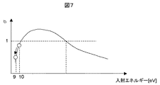
前者1)の方法では、ウェハに電子ビームを照射することにより生成される二次電子の放出効率が所定の値になるように、電子ビームの電子エネルギーを制御する。帯電極性は二次電子放出効率により定まり、二次電子放出効率が1以上であれば正に、1以下であれば負に帯電する。二次電子放出効率と電子エネルギーの関係を図7に示す。
In order to charge the wafer, there are 1) a method of irradiating the wafer with an electron beam and a method of using a charge control electrode. The principle will be described below.
In the former method 1), the electron energy of the electron beam is controlled so that the emission efficiency of secondary electrons generated by irradiating the wafer with the electron beam becomes a predetermined value. The charging polarity is determined by the secondary electron emission efficiency. When the secondary electron emission efficiency is 1 or more, the charge polarity is positive, and when it is 1 or less, the charge is negative. FIG. 7 shows the relationship between secondary electron emission efficiency and electron energy.
後者2)の方法では、ウェハに対する帯電制御電極への印加電位を制御することで帯電極性を制御する。ウェハに対して、帯電制御電極に正電圧を印加すれば正に、負電圧を印加すれば負に帯電する。つまりウェハから放出された二次電子を、引上げる方向に電場を形成すると正に帯電し、引戻す方向に電場を形成すると負に帯電する。 In the latter method 2), the charging polarity is controlled by controlling the potential applied to the charging control electrode for the wafer. The wafer is positively charged when a positive voltage is applied to the charge control electrode, and negatively charged when a negative voltage is applied. That is, the secondary electrons emitted from the wafer are positively charged when an electric field is formed in the pulling direction, and negatively charged when an electric field is formed in the pulling direction.
ウェハ表面を帯電させる際には、検査対象となる領域を均一に帯電させなければならない。ウェハ表面が不均一に帯電すると、二次電子の軌道が大きく曲がり二次電子検出効率に影響を及ぼすためである。この結果、例えば、取得画像に歪みや明るさムラが発生し、欠陥検出精度が劣化する。ウェハ表面が不均一に帯電する原因としては、
(1)負帯電の形成方法が原因となる場合、
(2)ウェハ表面に形成された回路パターンが原因となる場合、等がある。
以下、これら二つの例について説明する。
はじめに、負帯電形成方法が原因となって不均一な帯電を引起す理由を説明する。負帯電を形成する方法として帯電制御電極を利用する方法が特開平11−121561に開示されている。
When charging the wafer surface, the region to be inspected must be uniformly charged. This is because if the wafer surface is charged non-uniformly, the trajectory of the secondary electrons is greatly bent and affects the secondary electron detection efficiency. As a result, for example, distortion and brightness unevenness occur in the acquired image, and the defect detection accuracy deteriorates. As a cause of uneven charging of the wafer surface,
(1) When the negative charge formation method causes
(2) There are cases where the circuit pattern formed on the wafer surface is the cause.
Hereinafter, these two examples will be described.
First, the reason why non-uniform charging is caused by the negative charge forming method will be described. Japanese Patent Application Laid-Open No. 11-121561 discloses a method of using a charge control electrode as a method of forming a negative charge.
特開平11−121561は、当該特許文献の図5に示されるようにウェハ直上に設置した電極(帯電制御電極807)に負電圧を印加することでウェハ直上に電位障壁を形成し、電子線801を照射することで生じる二次電子809をウェハに引戻し、ウェハ表面に吸着させ負帯電を形成している。この方法では、電子線照射領域だけが負に帯電するため、負帯電していない照射領域周辺との間に電界が発生する。この電界により表面に吸着している電子が拡散し、欠陥部と正常部の電位差がなくなるためコントラストに差がなくなり検査精度が低下する。
In Japanese Patent Laid-Open No. 11-121561, as shown in FIG. 5 of the patent document, a potential barrier is formed immediately above the wafer by applying a negative voltage to an electrode (charging control electrode 807) placed immediately above the wafer. The
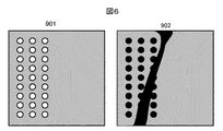
次に、ウェハ表面に形成された回路パターンが不均一な帯電を引起す理由を、図6を用いて説明する。図6に示すような、検査領域の左半分に回路パターンとしてプラグが形成され、右半分にはパターンが何も形成されていない場合を考える。このようなパターンに二次電子を引戻すと、プラグ804は基板と導通しているため帯電しないが、絶縁膜は負に帯電する。図6に示すパターンでは、左半分はプラグが密にあるため、右半分のパターンが無い領域より帯電電位が高い。左半分と右半分で帯電電位が異なるため、電界が生じ、二次電子軌道が曲がる。そのため、図6に示すようなウェハパターン901の電位コントラスト像902を取得すると、シェーディングが発生し、欠陥検査精度が劣化する。
Next, the reason why the circuit pattern formed on the wafer surface causes non-uniform charging will be described with reference to FIG. Consider a case in which a plug is formed as a circuit pattern in the left half of the inspection region and no pattern is formed in the right half as shown in FIG. When secondary electrons are pulled back to such a pattern, the
以上の(1)(2)の説明では、パターン検査の実行時に不均一な帯電が発生することを説明したが、検査装置で検査する前に、既にウェハが帯電している場合もある。様々な加工プロセスを経てきた結果の帯電であるため帯電状態は不均一であり、正負のどちらに帯電しているかも不明である。
不均一な帯電を均一にする帯電制御方法として、紫外光と電子ビームによるプリチャージを用いる方法が知られている。
紫外光による帯電制御方法は例えば、特開2003−151483に開示されている。この技術は試料に蓄積された電子を紫外光照射により、光電子放出もしくは試料表面を導電化することで帯電を均一にする。
In the explanations of (1) and (2) above, it has been explained that non-uniform charging occurs during the execution of pattern inspection. However, the wafer may already be charged before inspection by the inspection apparatus. Since it is the charge resulting from various processing processes, the charged state is non-uniform and it is unclear whether it is positive or negative.
As a charging control method for making non-uniform charging uniform, a method using precharging with ultraviolet light and an electron beam is known.
A charging control method using ultraviolet light is disclosed in, for example, Japanese Patent Application Laid-Open No. 2003-151383. In this technique, the electrons accumulated in the sample are irradiated with ultraviolet light to emit photoelectrons or make the surface of the sample conductive to make the charge uniform.
また、プリチャージにより帯電を制御する方法は、例えば、特開2000−208085号公報に開示されている。特開2000−208085号公報に開示された発明では、画像取得用の電子源とは別な電子源を用いて、画像取得前に画像を取得しようとする対象領域の周辺の領域を負帯電させる(プリチャージ)。その後、画像取得用の電子源から放出される電子ビームを照射し、画像取得を行う。プリチャージ用の電子源から放出される電子ビームの電子エネルギーは、二次電子放出効率が1以下となるように制御される。 A method for controlling charging by precharging is disclosed in, for example, Japanese Patent Application Laid-Open No. 2000-208085. In the invention disclosed in Japanese Patent Application Laid-Open No. 2000-208085, an electron source different from the electron source for image acquisition is used to negatively charge the area around the target area to be acquired before acquiring the image. (Precharge). Thereafter, the electron beam emitted from the electron source for image acquisition is irradiated to acquire the image. The electron energy of the electron beam emitted from the precharge electron source is controlled so that the secondary electron emission efficiency is 1 or less.
上述の通り、被検査対象物の帯電状態を制御する上で、以下のような問題がある。
(1)帯電を制御する領域の回路パターンや帯電を制御する方法によっては、不均一な帯電を引起すことがある。
(2)荷電粒子線装置内へ搬入される以前に、既にウェハが不均一に帯電している場合があり、帯電の極性も不明である。
これらの問題により、シェーディング、像の歪み、フォーカスのずれなどの問題が起こる。これらのシェーディング、像の歪み、フォーカスのずれなどの問題は、二次電子画像を応用した装置において種々の二次的な問題を引き起こし、例えば、SEM式外観検査装置では欠陥検査精度の劣化、レビューSEMでは電位コントラストの低下による検査スループットの低下、測長SEMではコントラストの低下による測長精度の低下といった問題を引起こす。
As described above, there are the following problems in controlling the charged state of the object to be inspected.
(1) Depending on the circuit pattern of the region for controlling charging and the method for controlling charging, non-uniform charging may be caused.
(2) Before being carried into the charged particle beam apparatus, the wafer may already be charged unevenly, and the polarity of the charge is unknown.
These problems cause problems such as shading, image distortion, and focus shift. These problems such as shading, image distortion, and out-of-focus cause various secondary problems in devices using secondary electron images. For example, in SEM visual inspection equipment, defect inspection accuracy deteriorates and reviews. SEM causes problems such as a decrease in inspection throughput due to a decrease in potential contrast, and length measurement SEM causes problems such as a decrease in length measurement accuracy due to a decrease in contrast.
特開2003−151483号公報に開示された、紫外線照射により帯電制御を行なう技術では、ウェハの帯電を負から正にすることは可能であるが、正から負に帯電させることはできない。また、特開2000−208085号公報に開示されたプリチャージによって帯電状態を制御する技術では、ウェハの帯電を均一にする場合、プリチャージする前にウェハの帯電分布を知っておかねばならず、所望の帯電状態を形成することが困難であった。例えば、局所的に帯電しているウェハ上のある領域を、任意の帯電に制御する場合、帯電制御に必要な電荷量および照射エネルギーが不明であるため、帯電制御が困難であった。 With the technique for controlling charging by ultraviolet irradiation disclosed in Japanese Patent Application Laid-Open No. 2003-151383, the wafer can be charged from negative to positive, but cannot be charged from positive to negative. Further, in the technique for controlling the charging state by precharging disclosed in Japanese Patent Application Laid-Open No. 2000-208085, when making the charging of the wafer uniform, the charge distribution of the wafer must be known before precharging, It was difficult to form a desired charged state. For example, when a region on a locally charged wafer is controlled to an arbitrary charge, charge control is difficult because the charge amount and irradiation energy necessary for charge control are unknown.
そこで、本発明は、被検査対象物の帯電状態を従来よりも均一に制御することにより、従来よりも画質の高い電位コントラスト像を取得することが可能で、かつ従来よりも検査精度・測長精度の優れた荷電粒子線応用検査装置および検査方法を実現することを目的とする。 Therefore, the present invention makes it possible to obtain a potential contrast image with higher image quality than before by controlling the charged state of the object to be inspected more uniformly than in the past, and inspecting accuracy and length measurement more than in the past. An object of the present invention is to realize a charged particle beam applied inspection apparatus and inspection method with excellent accuracy.
本発明の発明者らは、従来よりも均一な帯電制御を実現するためには、以下の3つの課題を解決する必要があるという結論に想到した。
(i)帯電電位をウェハスケールで均一に、精確に制御する必要がある
(ii)正負、両方の極性に対応する必要がある
(iii)画像取得時、二次電子を効率的に検出する必要がある
といった課題がある。
The inventors of the present invention have come to the conclusion that it is necessary to solve the following three problems in order to achieve more uniform charge control than before.
(I) It is necessary to control the charging potential uniformly and accurately on the wafer scale. (Ii) It is necessary to deal with both positive and negative polarities. (Iii) It is necessary to detect secondary electrons efficiently during image acquisition. There is a problem that there is.
本発明では、上記(i)、(ii)の課題を解決するために、紫外光照射と帯電制御電極を連携して動作させることで、ウェハスケールで帯電を均一にする。次に、課題(iii)を解決するために、電位コントラスト像取得時には帯電制御電極に正電圧を印加する。これにより、上記の課題(i)〜(iii)を解決し、従来技術よりも均一性に優れた帯電制御を達成する。 In the present invention, in order to solve the above problems (i) and (ii), the charging is made uniform on the wafer scale by operating the ultraviolet light irradiation and the charge control electrode in cooperation. Next, in order to solve the problem (iii), a positive voltage is applied to the charge control electrode when acquiring a potential contrast image. As a result, the above problems (i) to (iii) are solved, and the charge control with higher uniformity than that of the prior art is achieved.
本発明によれば、回路パターンを有する半導体装置等の部分的に完成した基板の検査において、従来、検査前に基板が帯電しているために、像にシェーディングが発生し、そのため検査精度が劣化するという問題を解決することができる。帯電除去に電子ビームではなく紫外光を用い、帯電制御電極と連携して動作させることで、基板の帯電を広範囲に均一にすることが可能になった。また、シェーディングが発生しない像取得方法を発明することで、シェーディングの発生を無くし検査精度を向上させることができる。 According to the present invention, in the inspection of a partially completed substrate such as a semiconductor device having a circuit pattern, since the substrate is conventionally charged before the inspection, shading occurs in the image, and therefore the inspection accuracy deteriorates. Can solve the problem. By using ultraviolet light instead of an electron beam for charge removal and operating in conjunction with the charge control electrode, it has become possible to make the substrate uniformly charged over a wide range. Further, by inventing an image acquisition method that does not cause shading, it is possible to eliminate the occurrence of shading and improve the inspection accuracy.
図8には、紫外光照射と帯電制御電極への正電位印加との連携動作による帯電制御の原理について示す。ウェハ1102に紫外光64を照射する際に、帯電制御電極1107に正電位を印加する。帯電制御電極1107には、帯電制御電源1108から正電圧が印加される。よって、紫外光照射により生じた光電子1109は、帯電制御電極に印可された正電位による正電界に引寄せられ、ウェハから引上げられる。従って、光電子を失ったウェハは正に帯電する。
FIG. 8 shows the principle of charge control by cooperative operation of ultraviolet light irradiation and application of a positive potential to the charge control electrode. When irradiated with
図9には、紫外光照射と帯電制御電極への負正電位印加との連携動作による帯電制御の原理について示す。ウェハ1202に紫外光64を照射すると、ウェハ中に電子・正孔対が発生する。正孔はウェハ中を拡散し、再結合するが、電子は真空中に放出される。この際、帯電制御電極1207に帯電制御電源1208により負電圧を印加しておくと、電極の周囲に形成される負の電場により光電子1209はウェハに引戻される。帯電制御電極により引戻された光電子は表面準位に捕獲され、ウェハ表面に局在するため、全体として負に帯電する。
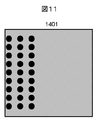
帯電制御電極に正電位を印加する場合には、ウェハから放出される二次電子の検出効率が上がるという副次的な効果もある。図10には、この様子を示す。この結果、図11に示すようなシェーディングの無い像1401を取得することが可能である。
FIG. 9 shows the principle of charge control by cooperative operation of ultraviolet light irradiation and application of a negative positive potential to the charge control electrode. When irradiated with
When a positive potential is applied to the charge control electrode, there is a secondary effect that the detection efficiency of secondary electrons emitted from the wafer is increased. FIG. 10 shows this state. As a result, an
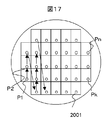
以上のように、ウェハの帯電状態は、ウェハに紫外光を照射し、ウェハから放出された光電子を帯電制御電極によって引上げるか、引戻すかで制御できる。また、ウェハの帯電電位は帯電制御電極に印加する電圧を制御することで制御することができる。例えば、ウェハの帯電電位を0Vにしたい場合は、図12に示すように、ウェハに紫外光を照射しながら、帯電制御電極の電位を10、−10、8、−8、6、−6、4、−4、2、−2、0Vというように制御することによって、ウェハの電位を0Vにすることが可能である。この方法によって、ウェハが正負どちらに帯電していても、帯電電位を0Vにすることができる。ウェハの帯電電位は、は0Vだけでなく任意の電位に帯電させることが可能である。また、ウェハ全面の帯電を均一にする場合は、紫外光を照射しつつ帯電制御電極の電位を一定にし、図16に示すようにウェハを走査すればよい。 As described above, the charged state of the wafer can be controlled by irradiating the wafer with ultraviolet light and pulling up or pulling back the photoelectrons emitted from the wafer by the charge control electrode. Further, the charging potential of the wafer can be controlled by controlling the voltage applied to the charging control electrode. For example, when it is desired to set the charging potential of the wafer to 0 V, the potential of the charging control electrode is set to 10, −10, 8, −8, 6, −6, while irradiating the wafer with ultraviolet light as shown in FIG. It is possible to set the wafer potential to 0V by controlling to 4, -4, 2, -2, 0V. By this method, the charged potential can be set to 0V regardless of whether the wafer is charged positively or negatively. The charged potential of the wafer can be charged not only to 0 V but also to an arbitrary potential. Further, in order to make the charging of the entire wafer surface uniform, the potential of the charging control electrode is made constant while irradiating ultraviolet light, and the wafer is scanned as shown in FIG.
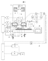
図1には、第1の実施例に係る検査装置の構成を示す。検査装置は、室内が真空排気される検査室2と、検査室2内に被検査基板9を搬送するための予備室(本実施例では図示せず)を備えており、この予備室は検査室2とは独立して真空排気できるように構成されている。また、検査装置は上記検査室2と予備室の他に制御部6、画像処理部から構成されている。検査室2内は大別して、電子光学系3、検出部、試料室8、光学顕微鏡部4、紫外光照射系から構成されている。
FIG. 1 shows the configuration of an inspection apparatus according to the first embodiment. The inspection apparatus includes an
紫外光照射系は、紫外光源63と図示されていない紫外光源制御装置からなり、紫外光源制御装置は、紫外光源と帯電制御電極65の電位制御が可能である。紫外光源は例えば、波長126nm、強度20Wの光源を用いることができる。
The ultraviolet light irradiation system includes an ultraviolet
電子光学系3は、電子銃10、電子ビーム引き出し電極11、コンデンサレンズ12、ブランキング用偏向器13、走査偏向器15、絞り14、対物レンズ16、反射板17、E×B偏向器18から構成されている。検出部7のうち、検出器20が検査室2内の対物レンズ16の上方に配置されている。検出器20の出力信号は、検査室2の外に設置されたプリアンプ21で増幅され、AD変換機22によりデジタルデータとなる。試料室8は、試料台30、Xステージ31、Yステージ32、回転ステージ33、位置モニタ用測長器34、被検査基板高さ測定器35から構成されている。
The electron
光学顕微鏡部4は、検査室2の室内における電子光学系3の近傍であって、互いに影響を及ぼさない程度離れた位置に設備されており、電子光学系3と光学顕微鏡部4の間の距離は既知である。そして、Xステージ31またはYステージ32が電子光学系3と光学顕微鏡部4の間の既知の距離を往復移動するようになっている。光学顕微鏡部4は光源40、光学レンズ41、CCDカメラ42により構成されている。画像処理部は、画像記憶部46、計算機48より構成されている。取り込まれた電子ビーム画像あるいは光学画像はモニタ50に表示される。
The
装置各部の動作命令および動作条件は、制御部6から入出力される。制御部6には、あらかじめ電子ビーム発生時の加速電圧、電子ビーム偏向幅、偏向速度、検出装置の信号取り込みタイミング、試料台移動速度等々の条件が、目的に応じて任意にあるいは選択して設定できるよう入力されている。制御部6は、補正制御回路43を用いて、位置モニタ用測長器34、被検査基板高さ測定器35の信号から位置や高さのずれをモニタし、その結果より補正信号を生成し、電子ビームが常に正しい位置に照射されるよう対物レンズ電源45や走査偏向器44に補正信号を送る。被検査基板9の画像を取得するためには、細く絞った電子ビーム19を該被検査基板9に照射し、二次電子および後方散乱電子51を発生させ、これらを電子ビーム19の走査およびステージ31、32の移動と同期して検出することで被検査基板9表面の画像を得る。
Operation commands and operation conditions of each part of the apparatus are input / output from the
電子銃10には拡散補給型の熱電界放出電子源が使用されている。この電子銃10を用いることにより、従来の、例えばタングステン(W)フィラメント電子源や、冷電界放出型電子源に比べて安定した電子ビーム電流を確保することができるため、明るさ変動の少ない電位コントラスト像が得られる。電子ビーム19は、電子銃10と引き出し電極11との間に電圧を印加することで電子銃10から引き出される。電子ビーム19の加速は、電子銃10に高電圧の負の電位を印加することでなされる。
The
これにより、電子ビーム19は、その電位に相当するエネルギーで試料台30の方向に進み、コンデンサレンズ12で収束され、さらに対物レンズ16により細く絞られて試料台30上のX−Yステージ31、32の上に搭載された被検査基板9(半導体ウエハ、チップあるいは液晶、マスク等微細回路パターンを有する基板)に照射される。なお、ブランキング用偏向器13には、走査信号およびブランキング信号を発生する信号発生器44が接続され、コンデンサレンズ12および対物レンズ16には、各々レンズ電源45が接続されている。被検査基板9には、高圧電源36により負の電圧(リターディング電圧)を印加できるようになっている。この高圧電源36の電圧を調節することにより一次電子ビームを減速し、電子銃10の電位を変えずに被検査基板9への電子ビーム照射エネルギーを最適な値に調節することができる。
Thereby, the
被検査基板9上に電子ビーム19を照射することによって発生した二次電子および後方散乱電子51は、基板9に印加された負の電圧により加速される。被検査基板9上方に、E×B偏向器18が配置され、これにより加速された二次電子および後方散乱電子51は所定の方向へ偏向される。E×B偏向器18にかける電圧と磁界の強度により、偏向量を調整することができる。また、この電磁界は、試料に印加した負の電圧に連動させて可変させることができる。E×B偏向器18により偏向された二次電子および後方散乱電子51は、所定の条件で反射板17に衝突する。この反射板17に加速された二次電子および後方散乱電子51が衝突すると、反射板17からは第二の二次電子および後方散乱電子52が発生する。
Secondary electrons and backscattered electrons 51 generated by irradiating the
検出部7は、真空排気された検査室2内の検出器20、検査室2の外のプリアンプ21、AD変換器22、光変換手段23、伝送手段24、電気変換手段25、高圧電源26、プリアンプ駆動電源27、AD変換器駆動電源28、逆バイアス電源29から構成されている。既に記述したように、検出部7のうち、検出器20が検査室2内の対物レンズ16の上方に配置されている。検出器20、プリアンプ21、AD変換器22、光変換器23、プリアンプ駆動電源27、AD変換器駆動電源28は、高圧電源26により正の電位にフローティングしている。上記反射板17に衝突して発生した第二の二次電子および後方散乱電子52は、この吸引電界により検出器20に導かれる。検出器20は、電子ビーム19が被検査基板9に照射されている間に発生した二次電子および後方散乱電子51がその後加速されて反射板17に衝突して発生した第二の二次電子および後方散乱電子52を、電子ビーム19の走査のタイミングと連動して検出するように構成されている。検出器20の出力信号は、検査室2の外に設置されたプリアンプ21で増幅され、AD変換器22によりデジタルデータとなる。
The detector 7 includes a
AD変換器22は、検出器20が検出したアナログ信号をプリアンプ21によって増幅された後に直ちにデジタル信号に変換して、画像処理部5に伝送するように構成されている。検出したアナログ信号を検出直後にデジタル化してから伝送するので、高速で且つSN比の高い信号を得ることができる。なお、ここでの検出器20として、例えば、半導体検出器を用いてもよい。
The
X−Yステージ31、32上には被検査基板9が搭載されており、検査実行時にはX−Yステージ31、32を静止させて電子ビーム19を二次元に走査する方法と、検査実行時にX−Yステージ31、32をY方向に連続して一定速度で移動されるようにして電子ビーム19をX方向に直線に走査する方法のいずれかを選択できる。ある特定の比較的小さい領域を検査する場合には前者のステージを静止させて検査する方法、比較的広い領域を検査するときは、ステージを連続的に一定速度で移動して検査する方法が有効である。なお、電子ビーム19をブランキングする必要がある時には、ブランキング用偏向器13により電子ビーム19が偏向されて、電子ビームが絞り14を通過しないように制御できる。
A
位置モニタ用測長器34として、本実施例ではレーザ干渉による測長計を用いた。Xステージ31およびYステージ32の位置が実時間でモニタでき、制御部6に転送されるようになっている。また、Xステージ31、Yステージ32、そして回転ステージ33のモータの回転数等のデータも同様に各々のドライバから制御部6に転送されるように構成されており、制御部6はこれらのデータに基いて電子ビーム19が照射されている領域や位置が正確に把握できるようになっており、必要に応じて実時間で電子ビーム19の照射位置の位置ずれを補正制御回路43より補正するようになっている。また、被検査基板毎に、電子ビームを照射した領域を記憶できるようになっている。
As the position monitor
光学式高さ測定器35は、電子ビーム以外の測定方式である光学式測定器、例えばレーザ干渉測定器や反射光の位置で変化を測定する反射光式測定器が使用されており、X−Yステージ上31、32に搭載された被検査基板9の高さを実時間で測定するように構成されている。本実施例では、スリットを通過した細長い白色光を透明な窓越しに被検査基板9に照射し、反射光の位置を位置検出モニタにて検出し、位置の変動から高さの変化量を算出する方式を用いた。この光学式高さ測定器35の測定データに基いて、電子ビーム19を細く絞るための対物レンズ16の焦点距離がダイナミックに補正され、常に非検査領域に焦点が合った電子ビーム19を照射できるようになっている。また、被検査基板9の反りや高さ歪みを電子ビーム照射前に予め測定しており、そのデータをもとに対物レンズ16の検査領域毎の補正条件を設定するように構成することも可能である。
The optical
画像処理部5は、画像記憶部46、計算機48、モニタ50により構成されている。上記検出器20で検出された被検査基板9の画像信号は、プリアンプ21で増幅され、AD変換器22でデジタル化された後に光変換器23で光信号に変換され、光ファイバ24によって伝送され、電気変換器25にて再び電気信号に変換された後に画像記憶部46に記憶される。
画像形成における電子ビームの照射条件および、検出系の各種検出条件は、あらかじめ検査条件設定時に設定され、ファイル化されてデータベースに登録されている。
The
The irradiation conditions of the electron beam in image formation and various detection conditions of the detection system are set in advance when setting the inspection conditions, and are filed and registered in the database.
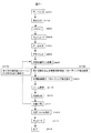
次に、図1で示した検査装置を用いて、検査を行う手順を図19に示すフローを用いて説明する。
まず、ステップ2201において、ウェハが任意の棚に設置されたウェハカセットを置く。操作画面50より、検査すべきウェハを指定するために、該ウェハがセットされたカセット内棚番号を指定する。そしてステップ2202において、モニタ50を含む入力手段により、各種検査条件を入力する。検査条件入力内容としては、電子ビーム電流、電子ビーム照射エネルギー、一画面の視野サイズ(FOV、Field of view)、リターディング電圧等である。個々のパラメータを入力することも可能であるが、通常は上記各種検査パラメータの組合わせが検査条件ファイルとしてデータベース化されており、それら範囲に応じた検査条件ファイルを選択して入力するだけでよい。
Next, a procedure for performing inspection using the inspection apparatus shown in FIG. 1 will be described using the flow shown in FIG.
First, in step 2201, a wafer cassette in which wafers are placed on an arbitrary shelf is placed. In order to designate a wafer to be inspected from the
ステップ2203において、入力手段に対する装置オペレータの入力を契機に自動検査をスタートする。まず、設定されたウェハ9を検査装置内にロードする(ステップ2204)。ウェハ搬送系においては、被検査ウェハ9の直径が異なる場合にも、ウェハ形状がオリエンテーションフラット型あるいはノッチ型のように異なる場合にも、ウェハ9を載置するためのホルダを、ウェハの大きさや形状にあわせて交換することにより対応できるようになっている。該被検査ウェハ9は、ウェハカセットからアーム、予備真空室等を含むウェハローダによりホルダ上に載置され、保持固定されてホルダとともにウェハローダ内で真空排気され、既に真空排気系で真空になっている検査室2に搬送される。
In step 2203, the automatic inspection is started by the input of the device operator to the input means. First, the
ウェハがロードされたら、ステップ2205において、上記入力された検査条件に基づき、制御部6より各部に電子ビーム照射条件が設定される。そして、ウェハホルダ上の第一のビーム校正用パターンが電子光学系下にくるようにステージ32が移動し、該ビーム校正用パターンの電位コントラスト像を取得し、該電位コントラスト像より焦点・非点を合わせる。そして、被検査ウェハ9上の所定の箇所に移動し、ウェハ9の電位コントラスト像を取得し、コントラスト等を調整する。ここで、電子ビーム照射条件等を変更する必要が生じた場合には、再度ビーム校正を実施することが可能である。同時にウェハ9の高さを高さセンサー15より求め、ウェハ高さ検出系35により高さ情報と電子ビームの合焦点条件の相関を求め、この後の電位コントラスト像取得時には毎回焦点合わせを実行することなく、ウェハ高さ検出の結果より合焦点条件に自動的に調整する。
When the wafer is loaded, in step 2205, the electron beam irradiation condition is set to each part by the
ステップ2206では、セットされたウェハ9は、光学顕微鏡部4でアラインメント用の第一の座標を観察するために、XYステージ32、33により移動される。モニタ50によりウェハ9上に形成されたアライメントパターンの光学顕微鏡画像が観察され、予め記憶された同じパターン画像と比較し、第一の座標の位置補正値が算出される。次に第一の座標から一定距離離れ第一の座標と同等の回路パターンが存在する第二の座標に移動し、同様に光学顕微鏡画像が観察され、アライメント用に記憶された回路パターン画像と比較され、第二の座標の位置補正値および第一の座標に対する回転ずれ量が算出される。
In step 2206, the
以上のようにして光学顕微鏡部4による所定の補正作業や検査領域設定等の準備作業が完了すると、XYステージ32、33の移動により、ウェハ9が電子光学系3の下に移動される。ウェハ9が電子光学系3の下に配置されると、上記光学顕微鏡部4により実施されたアライメント作業と同様の作業を電位コントラスト像により実施する。この際の電位コントラスト像の取得は、次の方法でなされる。上記光学顕微鏡画像による位置合せにおいて記憶され補正された座標値に基づき、光学顕微鏡部4で観察されたものと同じ回路パターンに、電子ビーム19が走査偏向器15によりXY方向に二次元に走査されて照射される。この電子ビームの二次元走査により、被観察部位から発生する放出電子51が上記の放出電子検出のための各部の構成および作用によって検出されることにより、電位コントラスト像が取得される。既に光学顕微鏡画像により簡便な検査位置確認や位置合せ、および位置調整が実施され、且つ回転補正も予め実施されているため、光学画像に比べ分解能が高く高倍率で高精度に位置合せや位置補正、回転補正を実施することができる。なお、電子ビーム19をウェハ9に照射すると、その箇所が帯電する。検査の際にその帯電の影響を避けるために、上記位置回転補正あるいは検査領域設定等の検査前準備作業において電子ビーム19を照射する回路パターンは予め被検査領域外に存在する回路パターンを選択するか、あるいは被検査チップ以外のチップにおける同等の回路パターンを制御部6から自動的に選択できるようにしておく。
When the preparatory work such as the predetermined correction work and inspection area setting by the
このようにして行ったアライメント結果は、各制御部に転送される。検査の際は、各制御部によって回転や位置座標が補正される。
アライメントが完了したら、試料ホルダ上に載置された第二の校正用パターンに移動する。第二の校正用パターンは、信号強度を検査で得られる電位コントラスト像の信号に一致させるものである。そのパターンは、十分低抵抗なビアホールと十分高抵抗なビアホールが加工されたパターンである。該パターンの電位コントラスト像を用いて十分な低抵抗部および高抵抗部の信号値を校正する。十分な高抵抗部はパターンの無い絶縁部を用いても良い。この結果をふまえて、ウェハ9上に移動し、ウェハ上のパターン箇所の電位コントラスト像を取得し、キャリブレーションを実施する(ステップ2207)。
The alignment result thus performed is transferred to each control unit. At the time of inspection, the rotation and position coordinates are corrected by each control unit.
When the alignment is completed, the second calibration pattern placed on the sample holder is moved. The second calibration pattern matches the signal intensity with the signal of the potential contrast image obtained by inspection. The pattern is a pattern in which a sufficiently low resistance via hole and a sufficiently high resistance via hole are processed. The signal values of the sufficiently low resistance portion and high resistance portion are calibrated using the potential contrast image of the pattern. An insulating part having no pattern may be used as the sufficiently high resistance part. Based on this result, the wafer moves onto the
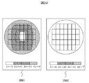
キャリブレーションが終了したら、ステップ2208において、検査領域Lkに移動する。続いて、ステップ2209において、ウェハの製造工程の際にウェハに蓄積された帯電(以下、残留帯電)を除去するために、紫外光を照射する。プロセス起因の帯電として例えばプラズマエッチングによる帯電が考えられる。プラズマエッチングでは、イオンや電子をウェハに照射し、シリコンとの化学的、物理的な反応により、ウェハ表面を加工する。ウェハが加工される時、イオンや電子などの荷電粒子に晒されるため電気的損傷を受け、プロセス後もウェハが帯電する。ステップ2209では、紫外光を照射すると同時に、ウェハの帯電を均一になるように、電源制御部66が帯電制御電位を制御する。すなわち、帯電制御電位Vccは図12に示すように、時間とともに帯電制御電位Vccの絶対値が小さくなるように電源制御部66によって制御される。この時、図16に示すように、ウェハ全面の残留帯電を除去してから次のステップに移ってもよいし、図18に示すように、検査領域の残留帯電を除去してから次のステップに移ってもよい。また、ウェハ全面の残留帯電除去はウェハロード(ステップ2204)直後におこなってもよい。
When the calibration is completed, in step 2208, the process moves to the inspection region Lk. Subsequently, in step 2209, ultraviolet light is irradiated to remove the charge accumulated in the wafer during the wafer manufacturing process (hereinafter referred to as residual charge). As charging due to the process, for example, charging by plasma etching can be considered. In plasma etching, ions and electrons are irradiated to a wafer, and the wafer surface is processed by chemical and physical reactions with silicon. When a wafer is processed, it is exposed to charged particles such as ions and electrons, so that it is electrically damaged, and the wafer is charged after the process. In step 2209, the power
従来は残留帯電によって、シェーディングが発生し、検査精度、欠陥検出感度が劣化するという問題があったが、検査前に残留帯電を除去することによってこの問題を解決することができた。本実施例記載の技術により、負極性の残留帯電だけでなく、正極性の残留帯電も除去することが可能になった。 Conventionally, there is a problem that shading occurs due to residual charge, and inspection accuracy and defect detection sensitivity deteriorate. However, this problem can be solved by removing the residual charge before inspection. The technique described in this example makes it possible to remove not only the negative residual charge but also the positive residual charge.
続いて、ステップ2210において、既に制御系7に入力されている電子照射条件帯電制御電位、リターディング電位を設定し、ステップ2211においてビームを照射し、ステップ2212において、検査を実施する。そのときに得られた電位コントラスト像は、紫外光による帯電除去を行っているため、シェーディングが発生することは無い。ステップ2213において、ステップ2212にて検出した欠陥の画像を保存する。 Subsequently, in step 2210, the electron irradiation condition charging control potential and the retarding potential already input to the control system 7 are set, the beam is irradiated in step 2211, and the inspection is performed in step 2212. Since the potential contrast image obtained at that time is subjected to charge removal by ultraviolet light, shading does not occur. In step 2213, the defect image detected in step 2212 is stored.
上記、検査走査を、ステップ2217に示すように以下の手順で繰返す。領域Lkへ移動(ステップ2208)→紫外光を照射および帯電を均一にするための帯電制御電位、リターディング電位設定(ステップ2209)→像取得のための帯電制御電位、リターディング電位設定(ステップ2210)→ビーム照射(ステップ2211)→領域Lkを検査(ステップ2212)→欠陥画像取得(ステップ2213)。
The above-described inspection scan is repeated in the following procedure as shown in
次の検査領域に移動する際は、XYステージ32、33を静止させて電子ビーム19の走査域を移動させる方法と、XYステージ32、33を移動させる方法のいずれかを選択できる。ある特定の比較的小さい領域を検査する場合には前者のステージを静止させて検査する方法、比較的広い領域を検査するときは、ステージを移動して検査する方法が有効である。なお、検査領域を移動する場合、電子ビーム19をブランキングする必要がある時には、ブランキング用偏向器13により電子ビーム19を偏向し、電子ビームがウェハに照射されないように制御できる。
また、既に検査した領域の帯電の影響を除去するために、紫外光による帯電除去を再度行っても良い。
When moving to the next inspection area, either a method of moving the scanning area of the
Further, in order to remove the influence of charging in the already inspected area, the charging removal by ultraviolet light may be performed again.
このように指定された領域の検査を実施しながら、ウェハ全域もしくは、部分的に検査し、ステップ2214において、検査結果を保存する。検査が完了したら、ステップ2215においてウェハをアンロードし、ステップ2216において終了する。
以上の検査方法により、従来問題になっていた検査前のウェハの帯電を除去することが可能になり、帯電によるシェーディングを無くすことができた。その結果、検査精度、欠陥検出感度を向上させることができた。
While inspecting the designated area as described above, the entire wafer or a part of the wafer is inspected, and in step 2214, the inspection result is stored. When the inspection is complete, the wafer is unloaded at step 2215 and the process ends at step 2216.
By the above inspection method, it was possible to remove the charge of the wafer before the inspection, which was a problem in the past, and it was possible to eliminate the shading due to the charge. As a result, inspection accuracy and defect detection sensitivity could be improved.
本実施例では、第一の実施例で説明した検査装置を用いて、ウェハを所望の帯電電圧にした状態で電位コントラスト像を取得し、欠陥検査を行うものである。
そのために、検査画像の取得直前に帯電制御電極に電子に対する電位障壁が−5Vになるような電圧を印加し、紫外光を照射しながら(図19ステップ2209)、ウェハ全面に紫外光が照射されるようにステージを走査した。帯電電位は、帯電制御電極の電位にほぼ等しくすることができ、かつウェハ全面に紫外光を照射するため、ウェハ全面を均等に−5V帯電させることができた。
In this embodiment, using the inspection apparatus described in the first embodiment, a potential contrast image is acquired in a state where the wafer is set to a desired charging voltage, and defect inspection is performed.
For this purpose, immediately before the inspection image is acquired, a voltage is applied to the charge control electrode such that the potential barrier against electrons becomes −5 V, and ultraviolet light is irradiated while irradiating ultraviolet light (step 2209 in FIG. 19). The stage was scanned as follows. The charging potential can be made substantially equal to the potential of the charge control electrode, and the entire surface of the wafer is irradiated with ultraviolet light, so that the entire surface of the wafer can be charged uniformly by -5V.
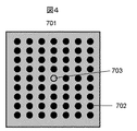
その後、帯電制御電極の電位をウェハに対して1000Vにすることによって(図19ステップ2210)、検査を開始した。走査電子ビーム照射の際に発生した二次電子は、1000Vにした帯電制御電極によって加速され、効率よく検出器まで導くことができるので、図4に示すような信号量が多く、ノイズが少なく、シェーディングの無い負帯電コントラスト像701を得ることができた。その結果、導通不良、ショート欠陥の検出感度を向上させることができた。
Thereafter, the inspection was started by setting the potential of the charge control electrode to 1000 V with respect to the wafer (step 2210 in FIG. 19). The secondary electrons generated during the scanning electron beam irradiation are accelerated by the charge control electrode set to 1000 V and can be efficiently guided to the detector. Therefore, the signal amount as shown in FIG. 4 is large, the noise is small, A negatively charged
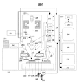
本実施例では、測長SEMを用いて、ウェハに形成されたパターンの測長をおこなった例について説明する。
図2に、測長SEMの構成の一例を示す。本装置は、電子光学系221、ステージ機構系222、ウェハ搬送系223、真空排気系224、光学顕微鏡225、制御系226、操作部227より構成されている。電子光学系221は、電子銃228、コンデンサレンズ229、対物レンズ230、二次電子検出器231、エネルギーフィルタ234、偏向器235、反射板236、ウェハ高さ検出器237より構成されている。ステージ機構系222は、XYステージ238、および試料としてのウェハを載置するためのホルダ239、ホルダ239およびウェハ251に負の電圧を印加するためのリターディング電源240より構成されている。
In this embodiment, an example will be described in which a length measurement of a pattern formed on a wafer is performed using a length measurement SEM.
FIG. 2 shows an example of the configuration of the length measurement SEM. This apparatus includes an electron
XYステージ238には、レーザ測長による位置検出器が取り付けられている。ウェハ搬送系223はカセット載置部241とローダ242より構成されており、ホルダ239はウェハ251を載置した状態でローダ242とXYステージ238を行き来するようになっている。制御系226は、信号検出系制御部243、ビーム偏向補正制御部244、電子光学系制御部245、ウェハ高さセンサ検出系246、機構・ステージ制御部247より構成されている。操作部227は、操作画面および操作部248、画像処理部249、画像・測長データ保存部250より構成されている。
A position detector based on laser length measurement is attached to the
次に、図2の各部の動作について、図20に示すフローを用いて説明する。
まず、ステップ2301において、ウェハ251が任意の棚に設置されたウェハカセットを、図2のウェハ搬送系223におけるカセット載置部241に置く。
次に、ステップ2302において、操作画面248より、測長すべきウェハ251を指定するために、該ウェハ251がセットされたカセット内棚番号を指定する。また、ウェハ加工データに基づいて測長すべきパターンの位置情報を格納している設定ファイルを操作画面248を選択する。選択においては、ネットワーク等による通信で設定ファイルを読み込む場合や、フレキシブルディスクのような記憶媒体より設定ファイルを読み込むことが可能である。
Next, the operation of each part in FIG. 2 will be described using the flow shown in FIG.
First, in step 2301, the wafer cassette on which the wafer 251 is placed on an arbitrary shelf is placed on the cassette mounting portion 241 in the
Next, in step 2302, in order to specify the wafer 251 to be measured from the
いずれの場合も、設定ファイル名を指定することにより、該測長パターンの各種データをデータ入力部56に読み込み、データ変換部257により測長SEMで用いているデータ形式および座標系に変換することがある。測長を実行するために必要な条件の入力を完了し、ステップ2303において、オペレータの条件入力を契機にして測長のシーケンスをスタートする。ステップ2304において、まず、設定されたウェハ251をレビュー装置内に搬送する。ウェハ搬送系223においては、被検査ウェハの直径が異なる場合にも、ウェハ形状がオリエンテーションフラット型あるいはノッチ型のように異なる場合にも、ウェハ251を載置するホルダ239をウェハの大きさや形状にあわせて交換することにより対応できるようになっている。該被測長ウェハは、カセットからアーム、予備真空室等を含むウェハローダ242によりホルダ239上に載置され、保持固定されてホルダとともに検査室に搬送される。
In either case, by specifying the setting file name, various data of the length measurement pattern are read into the data input unit 56 and converted into the data format and coordinate system used in the length measurement SEM by the
ステップ2304において、ウェハ51がロードされたら、ステップ2305では、上記入力された測長条件に基づき、電子光学系制御部245より各部に電子線照射条件が設定される。そして、ウェハ251の所定箇所の電子線画像を取得し、該画像より焦点・非点を合わせる。また、同時にウェハ251高さを高さ検出器237より求め、高さ情報と電子ビームの合焦点条件の相関を求め、この後の電子線画像取得時には毎回焦点合わせを実行することなく、ウェハ高さ検出の結果より合焦点条件に自動的に調整する。
In
電子線照射条件および焦点・非点調整が完了したら、ステップ2306において、ウェハ上の2点によりアライメントを実施する。
アライメントが完了したら、アライメント結果に基づき回転や座標値を補正し、ステップ2307において読み込んだ設定ファイルの各種情報に基づき、測長すべきパターンの位置に移動する。
ここで図22に示すように測長対象のウェハの電位分布2501が、帯電により面内で数10V程度ばらついている場合がある。この場合、帯電によってフォーカスがずれるため、図24に示すように測長対象パターン2701の輪郭が不明確になり、測長データ2702の精度が劣化するという問題があった。
When the electron beam irradiation conditions and the focus / astigmatism adjustment are completed, in step 2306, alignment is performed using two points on the wafer.
When the alignment is completed, the rotation and coordinate values are corrected based on the alignment result, and the position is moved to the position of the pattern to be measured based on various information in the setting file read in
Here, as shown in FIG. 22, the
そこで、測長する前にウェハ全面の帯電を均一にする必要がある。帯電を均一にするためにステップ2308において紫外光を照射しつつ帯電制御電位、リターディング電位を制御する。帯電制御電位は図12に示すように、時間とともに帯電制御電位の絶対値が小さくなるように制御する。紫外光を照射することにより、ウェハ全面にわたって均一な電位分布2502を得ることができた。ウェハに印加する帯電制御電圧としては、図12に示したパルス形状の電圧信号だけではなく、交流電圧を極性を変化させて印加してもよい。この場合、耐電制御電極へは交流電源が接続されることになる。
Therefore, it is necessary to uniformly charge the entire surface of the wafer before measuring. In order to make the charging uniform, in
帯電を均一にした後、ステップ2309において図10に示すように帯電制御電位をウェハに対して正電位になるように設定し、ステップ2310においてビームを照射し、ステップ2311で測長すべきパターンに移動し、ステップ2312において被測長パターンの画像および測長データを取得する。ウェハの帯電が均一であるため、測長対象パターン2703の輪郭は明確であり、測長データ2704を精度良く取得することができた。
なお、本実施例では図16に示すように紫外光を照射してウェハ全面の帯電を均一してから、図17に示すように測長パターンの画像および測長データを取得しているが、図15に示すように、欠陥画像を取得するつど紫外光を照射し、被測長パターンの帯電を均一にしてもよい。
After uniform charging, the charge control potential is set to be positive with respect to the wafer in step 2309 as shown in FIG. 10, the beam is irradiated in step 2310, and the pattern to be measured in step 2311 is obtained. In step 2312, an image of the pattern to be measured and the length measurement data are acquired. Since the wafer was uniformly charged, the outline of the length
In this embodiment, as shown in FIG. 16, the ultraviolet light is irradiated to make the entire surface of the wafer uniform, and then the measurement pattern image and measurement data are acquired as shown in FIG. As shown in FIG. 15, it is also possible to irradiate ultraviolet light every time a defect image is acquired, and to uniformly charge the pattern to be measured.
ステップ2313において、取得された画像および測長データは、必要に応じて画像・データ保存部250に保存される。保存するか否かは予め、設定ファイルで設定しておく。
上記、画像保存および測長データ取得操作を、ステップ2316に示すように以下の手順で繰返す。測長パターン位置へ移動(ステップ2311)→画像取得およびパターン測長(ステップ2312)→画像、測長データ保存(ステップ2313)。
1枚のウェハにおいて、測長を指定されたパターン全部について上記一連の動作が完了したら、ステップ2314において、ウェハをアンロードし、ステップ2315において測長を終了する。
In step 2313, the acquired image and length measurement data are stored in the image / data storage unit 250 as necessary. Whether or not to save is set in advance in a setting file.
The above-described image storage and length measurement data acquisition operations are repeated in the following procedure as shown in
When the above-described series of operations is completed for all the patterns for which length measurement is specified for one wafer, the wafer is unloaded in step 2314 and the length measurement is terminated in
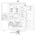
本実施例では、レビューSEMを用いて、欠陥分類をおこなった例について説明する。
図3に、レビューSEMの構成の一例を示す。本装置は、電子光学系321、ステージ機構系322、ウェハ搬送系323、真空排気系324、光学顕微鏡325、制御系326、操作部327より構成されている。電子光学系321は、電子銃328、コンデンサレンズ329、対物レンズ330、第一の検出器331、第二の検出器332、第三の検出器333、エネルギーフィルタ334、偏向器335、反射板336、ウェハ高さ検出器337より構成されている。ステージ機構系322は、XYステージ338、および試料としてのウェハを載置するためのホルダ339、ホルダ339およびウェハ351に負の電圧を印加するためのリターディング電源340より構成されている。
In this embodiment, an example in which defect classification is performed using a review SEM will be described.
FIG. 3 shows an example of the configuration of the review SEM. This apparatus includes an electron
XYステージ338には、レーザ測長による位置検出器が取り付けられている。ウェハ搬送系323はカセット載置部341とローダ342より構成されており、ホルダ339はウェハ351を載置した状態でローダ342とXYステージ338を行き来するようになっている。制御系326は、信号検出系制御部343、ビーム偏向補正制御部344、電子光学系制御部345、ウェハ高さセンサ検出系346、機構・ステージ制御部347より構成されている。操作部327は、操作画面および操作部348、画像処理部349、画像・検査データ保存部350より構成されている。また、図3のレビューSEMは、紫外線照射のための紫外線照射系を備える。紫外光照射系は、紫外光源363と紫外光源制御装置367を備える。紫外光源は例えば、波長126nm、強度20Wの光源を用いることができる。紫外光源制御装置367は紫外光源363に印加する電圧を制御する。一方、電源制御部365は、帯電制御電極364へ印加する電圧を制御する。
A position detector based on laser length measurement is attached to the
次に、図3の各部の動作について、図21に示すフローを用いて説明する。
まず、ステップ2401において、ウェハ351が任意の棚に設置されたウェハカセットを、図3のウェハ搬送系323におけるカセット載置部341に置く。
次に、ステップ2402において、操作画面348より、レビューすべきウェハ351を指定するために、該ウェハ351がセットされたカセット内棚番号を指定する。また、レビューにおいては、他の検査装置により検査を実施され、欠陥等の位置情報を含む検査結果情報をもとに電子線画像による観察を実行するため、操作画面348より検査結果ファイルを選択する。選択においては、ネットワーク等による通信で検査結果ファイルを読み込む場合や、フレキシブルディスクような媒体より検査結果ファイルを読み込むことが可能である。
Next, the operation of each part in FIG. 3 will be described using the flow shown in FIG.
First, in step 2401, the wafer cassette in which the
Next, in step 2402, in order to specify the
いずれの場合も、検査結果ファイル名を指定することにより、該検査結果の各種データをデータ入力部356に読み込み、データ変換部357によりレビューSEMで用いているデータ形式および座標系に変換することがある。さらに、操作画面348より、レビュー条件ファイル名を入力する。このレビュー条件ファイルは、レビューの内容を決めるための各種パラメータを組み合わせて構成されたものである。レビューを実行するために必要な条件の入力を完了し、ステップ2403において、装置オペレータの入力を契機にして自動レビューのシーケンスをスタートする。
In any case, by specifying the inspection result file name, various data of the inspection result can be read into the
まず、設定されたウェハ351をレビュー装置内に搬送する。ウェハ搬送系323においては、被検査ウェハの直径が異なる場合にも、ウェハ形状がオリエンテーションフラット型あるいはノッチ型のように異なる場合にも、ウェハ351を載置するホルダ339をウェハの大きさや形状にあわせて交換することにより対応できるようになっている。該被検査ウェハは、カセットからアーム、予備真空室等を含むウェハローダ342によりホルダ339上に載置され、保持固定されてホルダとともに検査室に搬送される。
First, the
ステップ2404において、ウェハ351がロードされたら、ステップ2405では、上記入力されたレビュー条件に基づき、電子光学系制御部345より各部に電子線照射条件が設定される。そして、ウェハ351の所定箇所の電子線画像を取得し、該画像より焦点・非点を合わせる。また、同時にウェハ351高さを高さ検出器337より求め、高さ情報と電子ビームの合焦点条件の相関を求め、この後の電子線画像取得時には毎回焦点合わせを実行することなく、ウェハ高さ検出の結果より合焦点条件に自動的に調整する。これにより、高速連続電子線画像取得が可能になった。
In step 2404, when the
電子線照射条件および焦点・非点調整が完了したら、ステップ2406において、ウェハ上の2点によりアライメントを実施する。
アライメントが完了したら、ステップ2407において、アライメント結果に基づき回転や座標値を補正し、既に読み込んだ検査結果ファイルの各種情報に基づき、レビューすべき欠陥の位置に移動する。
欠陥位置に移動したら、欠陥部周辺の帯電を均一にするためにステップ2408において紫外光を照射しつつ、帯電制御電位、リターディング電位を制御する。帯電制御電位は図12に示すように、時間とともにVcc電位の絶対値が小さくなるように制御する。紫外光を照射することにより、欠陥部周辺の帯電を均一にすることができた。また、この後、図13、図14に示すように帯電制御電位Vccを設定して、紫外光照射することにより、任意の電位に帯電させることも可能である。この帯電によりコンタクトホールの導通不良欠陥、ショート欠陥などの検出が可能になる。
When the electron beam irradiation conditions and focus / astigmatism adjustment are completed, in step 2406, alignment is performed using two points on the wafer.
When the alignment is completed, in step 2407, the rotation and coordinate values are corrected based on the alignment result, and the position is moved to the position of the defect to be reviewed based on various information of the already read inspection result file.
After moving to the defect position, the charge control potential and the retarding potential are controlled while irradiating with ultraviolet light in
帯電を均一にした後、ステップ2409において図10に示すように帯電制御電位をウェハに対して正電位に設定し、ステップ2410、2411において欠陥画像を取得する。従来は図6のようにシェーディングが生じていたが、本方法によってシェーディングを無くすことができた。
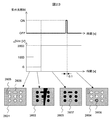
なお、本実施例では図15に示すように、欠陥画像を取得するつど紫外光を照射し、欠陥部周辺の帯電を均一にし像を取得している。これは図13に示す帯電制御方法により実現される。まず,正帯電コントラスト像を取得する場合,帯電制御電圧を基板に対して正電圧に設定し,紫外光を照射する。これにより,試料を所望の電位に帯電させ,その後紫外光を消灯し,正帯電コントラスト像を取得する。この時,図10で示すように帯電制御電圧は基板に対して正に設定する。 以上の紫外光照射の制御と帯電制御電圧の制御の関係は図13中の上段と中段の時間経過図に示す通りである。
After the charging is made uniform, the charge control potential is set to a positive potential with respect to the wafer as shown in FIG. 10 in step 2409, and defect images are acquired in
In this embodiment, as shown in FIG. 15, each time a defect image is acquired, ultraviolet light is irradiated to uniformly charge the periphery of the defect portion to acquire an image. This is realized by the charge control method shown in FIG. First, when acquiring a positively charged contrast image, the charging control voltage is set to a positive voltage with respect to the substrate, and ultraviolet light is irradiated. As a result, the sample is charged to a desired potential, then the ultraviolet light is turned off, and a positively charged contrast image is acquired. At this time, as shown in FIG. 10, the charging control voltage is set positive with respect to the substrate. The relationship between the above ultraviolet light irradiation control and charging control voltage control is as shown in the time lapse diagram of the upper and middle stages in FIG.
次に,負帯電コントラスト像を取得する場合,帯電制御電圧を基板に対して負電圧に設定し,紫外光を照射する。これにより,試料を所望の電圧に帯電させ,その後紫外光を消灯し負帯電コントラスト像を取得する。この時,図10で示すように帯電制御電極は,基板に対して正電圧に設定する。
以上の紫外光照射の制御と帯電制御電圧の制御の関係は図13中の上段と中下段の時間経過図に示す通りである。これらの動作を図15に示すように観察する欠陥ごとに繰返す。紫外光照射のオンオフは紫外光源制御装置367により、帯電制御電極337への電圧印加のオンオフは電源制御部365により実行される。また、紫外光源制御装置367と電源制御部365の動作のタイミング調整は制御系326により実行される。
Next, when acquiring a negatively charged contrast image, the charging control voltage is set to a negative voltage with respect to the substrate, and ultraviolet light is irradiated. As a result, the sample is charged to a desired voltage, and then the ultraviolet light is turned off to obtain a negatively charged contrast image. At this time, as shown in FIG. 10, the charge control electrode is set to a positive voltage with respect to the substrate.
The relationship between the above ultraviolet light irradiation control and charging control voltage control is as shown in the time lapse diagram of the upper and middle lower sections in FIG. These operations are repeated for each defect to be observed as shown in FIG. The ultraviolet light irradiation is turned on / off by the ultraviolet light
また,図15に示す帯電制御,画像取得方法の他にも,図16にしめすように紫外光を照射してウェハ全面の帯電を均一してから、図17に示すように欠陥部の画像を取得する方法もある。この方法で正帯電コントラスト像を取得する場合について図14を用いて説明する。まず,帯電制御電圧を図14中段のタイムチャートに示すように所望の正電圧に設定し,図14上段のタイムチャートに示すように紫外光を照射する。この時図16に示すようにウェハ全面に紫外光を照射する。後,図14上段タイムチャートのように紫外光を消灯し,帯電制御電圧は基板に対して正電圧に設定し順次欠陥を観察していく。 Further, in addition to the charging control and image acquisition method shown in FIG. 15, after the ultraviolet light is irradiated to make the entire surface of the wafer uniform as shown in FIG. 16, the image of the defective portion is displayed as shown in FIG. There is also a way to get it. A case where a positively charged contrast image is acquired by this method will be described with reference to FIG. First, the charging control voltage is set to a desired positive voltage as shown in the time chart in the middle of FIG. 14, and ultraviolet light is irradiated as shown in the upper time chart of FIG. At this time, the entire surface of the wafer is irradiated with ultraviolet light as shown in FIG. Thereafter, as shown in the upper time chart of FIG. 14, the ultraviolet light is turned off, the charging control voltage is set to a positive voltage with respect to the substrate, and the defects are sequentially observed.
次に,負帯電コントラスト像を取得する場合について図14を用いて説明する。まず,帯電制御電圧を図14下段のタイムチャートに示すように所望の負電圧に設定し,図14上段のタイムチャートに示すように紫外光を照射する。この時図16に示すようにウェハ全面に紫外光を照射する。後,図14上段タイムチャートのように紫外光を消灯し,帯電制御電圧は基板に対して正電圧に設定し順次欠陥を観察していく。 Next, a case where a negatively charged contrast image is acquired will be described with reference to FIG. First, the charging control voltage is set to a desired negative voltage as shown in the time chart in the lower part of FIG. 14, and ultraviolet light is irradiated as shown in the time chart in the upper part of FIG. At this time, the entire surface of the wafer is irradiated with ultraviolet light as shown in FIG. Thereafter, as shown in the upper time chart of FIG. 14, the ultraviolet light is turned off, the charging control voltage is set to a positive voltage with respect to the substrate, and the defects are sequentially observed.
ステップ2411において、取得された高倍率画像は、必要に応じて画像・データ保存部350に保存される。予め保存する、保存しないをレビュー条件ファイルで設定しておく。また、必要に応じて、複数の検出器による複数種類の画像を、設定に応じて同時に保存することが可能である。例えば、第二の検出器332で検出された二次電子による画像と、第一の検出器331で検出された反射電子による画像を同時に保存することが可能である。
ステップ2412において、画像を保存すると同時に、画像処理部349では画像情報より欠陥の特徴を抽出して、欠陥の内容を自動的に分類する。分類された結果を、例えば0〜255の数値にコード化し、該コード番号を検査結果ファイルのなかの欠陥分類コードに対応する箇所に書き込む。
In
In step 2412, at the same time as saving the image, the
上記、欠陥レビュー操作を、ステップ2416に示すように以下の手順で繰返す。欠陥位置へ移動(ステップ2407)→紫外光照射および、帯電を均一にするための帯電制御電位、リターディング電位設定(ステップ2408)→像取得のための帯電制御電位、リターディング電位設定(ステップ2409)→ビーム照射(ステップ2410)→画像取得(ステップ2411)→欠陥分類(ステップ2412)。
1枚のウェハにおいて、レビュー実施を指定された欠陥全部について上記一連の動作が完了したら、該ウェハの検査結果ファイル(分類結果を書き込まれたファイル)を自動的に保存し、指定された先に該検査結果ファイルを出力し、ステップ2414において、ウェハをアンロードし、ステップ2415においてレビューを終了する。
The defect review operation is repeated in the following procedure as shown in
When the above series of operations is completed for all the defects for which review is specified for a single wafer, the inspection result file (file in which the classification results are written) of the wafer is automatically saved, and the specified destination is saved. The inspection result file is output, the wafer is unloaded in
本方法を用いることにより、従来解決できなった、検査前にウェハが保持している残留帯電による検査精度の劣化、像取得の際に生じるシェーディングという問題を解決することができた。 By using this method, it was possible to solve the problems of the deterioration of inspection accuracy due to the residual charge held by the wafer before inspection and the shading that occurs during image acquisition, which could not be solved in the past.
本実施例では、実施例1で説明した検査装置が出力する欠陥位置情報に基づき、欠陥をレビューSEMで欠陥を観察、分類する方法についてコンタクトホールパターンを例に挙げて説明する。
コンタクトホール底の残渣、形状欠陥、導通不良欠陥を分類するには正負、両方の電位コントラスト像を取得する場合がある。
ステップ2410において、図23に示すように帯電制御電極とウェハの電位差(ΔVcc)を1000Vに設定してまず正帯電コントラスト像2601を取得し異物2605及び形状欠陥2606を抽出する。
In the present embodiment, a method for observing and classifying defects with a review SEM based on the defect position information output by the inspection apparatus described in the first embodiment will be described using a contact hole pattern as an example.
In order to classify the residue at the bottom of the contact hole, the shape defect, and the poor conduction defect, both positive and negative potential contrast images may be acquired.
In step 2410, as shown in FIG. 23, the potential difference (ΔVcc) between the charge control electrode and the wafer is set to 1000 V, and a positively charged
次に、ΔVcc=−5Vに設定することで二次電子に対して電位障壁を設け、一度放出された二次電子をウェハに引戻すことにより、ウェハを負帯電させる。この状態で像を取得すると、二次電子をウェハから引上げる電場が無いため二次電子軌道が広がり、シェーディングが発生した負帯電コントラスト像2602が取得される。
そこで、本実施例では、シェーディングの無い像を得るために、ΔVcc=2000Vに設定し、二次電子を引上げる電場を形成した。すると、シェーディングの無い像2603を得ることができ、導通不良欠陥2607を抽出することができた。続いて、導通不良欠陥2607の原因を特定するため、コンタクトホール底の正帯電コントラスト像2604を取得する。この時、コンタクトホール底からの二次電子を引上げるために、ΔVcc=2000Vに設定しているが、負帯電がウェハに残留しているため、従来は正帯電コントラストを得るまでに時間がかかっていた。この場合には、ウェハに紫外光を0.1s照射することで残留していた負帯電を除去し、正帯電コントラスト像2504を取得することができた。結果から、導通不良欠陥の原因が異物2608の付着であることを特定できた。
Next, by setting ΔVcc = −5 V, a potential barrier is provided for the secondary electrons, and the secondary electrons once emitted are pulled back to the wafer, thereby negatively charging the wafer. When an image is acquired in this state, since there is no electric field for pulling up secondary electrons from the wafer, the secondary electron trajectory widens, and a negatively charged
Therefore, in this embodiment, in order to obtain an image without shading, ΔVcc = 2000 V was set, and an electric field for pulling up secondary electrons was formed. As a result, an
以上、従来技術では、画像取得時にウェハの帯電を考慮に入れていないため、シェーディングや歪んだ画像を取得する場合があったが、本実施例の方法では、帯電制御時と画像取得時で、帯電制御電極に印加する電位を負から正へ切替えるため、シェーディングも発生せず、歪んだ画像を取得する確率を非常に低減することができた。
なお、本実施例では、ウェハを負帯電させるために帯電制御電極を用いたが、フラッドガンによるプリチャージ、紫外光照射を用いてもよい。
As described above, in the prior art, since the charging of the wafer is not taken into consideration at the time of image acquisition, there is a case of acquiring a shading or distorted image, but in the method of the present embodiment, at the time of charge control and at the time of image acquisition, Since the potential applied to the charge control electrode is switched from negative to positive, shading does not occur, and the probability of acquiring a distorted image can be greatly reduced.
In this embodiment, the charge control electrode is used to negatively charge the wafer. However, precharge using a flood gun or ultraviolet light irradiation may be used.
2:検査室、3:電子光学系、4:光学顕微鏡部、6:制御部、8:試料室、9:ウェハ、10:電子銃、11:引き出し電極、12:コンデンサレンズ、13:ブランキング偏向器、14:絞り、15:走査偏向器、16:対物レンズ、17:反射板、18:E×B偏向器、19:電子ビーム、20:検出器、21:プリアンプ、22:AD変換器、23:光変換器、24:光ファイバ、25:電気変換器、26:高圧電源、27:プリアンプ駆動電源、28:AD変換器駆動電源、29:逆バイアス電源、30:試料台、31:Xステージ、32:Yステージ、33:回転ステージ、34:位置モニタ測長器、35:被検査基板高さ測定器、36:リターディング電源、40:白色光源、41:光学レンズ、42:CCDカメラ、43:補正制御回路、44:走査信号発生器、45:対物レンズ電源、46:画像記憶部、48:計算機、50:モニタ、51:二次電子および後方散乱電子、52:第二の二次電子および後方散乱電子、62:試料交換室、63:紫外光源、64:紫外光、65:帯電制御電極、66:電源制御部、67:帯電制御電源、221:電子光学系、222:ステージ機構系、223:ウェハ搬送系、224:真空排気系、225:光学顕微鏡、226:制御系、227:操作部、228:電子銃、229:コンデンサレンズ、230:対物レンズ、231:第一の検出器、232:第二の検出器、234:反射板、235:偏向器、236:反射板、237:ウェハ高さ検出系、238:XYステージ:239:ホルダ、240:リターディング電源、241:カセット載置部、242:ウェハローダ、243:信号検出系制御部、244:ビーム偏向補正制御部、245:電子光学系制御部、246:ウェハ高さセンサ検出系、247:機構・ステージ制御部、248:操作画面・操作部、249:画像処理部、250:データ保存部、251:ウェハ、252:一次電子ビーム、253:反射電子、254:二次電子、255:高エネルギー成分二次電子、256:データ入力部、257:データ変換部、258:寸法測定部、263:紫外光源、264:帯電制御電極、265:帯電制御電極制御部、266:帯電制御電源、321:電子光学系、322:ステージ機構系、323:ウェハ搬送系、324:真空排気系、325:光学顕微鏡、326:制御系、327:操作部、328:電子銃、329:コンデンサレンズ、330:対物レンズ、331:第一の検出器、332:第二の検出器、333:第三の検出器、334:エネルギーフィルタ、335:偏向器、336:反射板、337:ウェハ高さ検出系、338:XYステージ:339:ホルダ、340:リターディング電源、341:カセット載置部、342:ウェハローダ、343:信号検出系制御部、344:ビーム偏向補正制御部、345:電子光学系制御部、346:ウェハ高さセンサ検出系、347:機構・ステージ制御部、348:操作画面・操作部、349:画像処理部、350:データ保存部、351:ウェハ、352:一次電子ビーム、353:反射電子、354:二次電子、355:高エネルギー成分二次電子、356:データ入力部、357:データ変換部、363:紫外光源、364:帯電制御電極、365:帯電制御電極制御部、366:帯電制御電源、401:一次電子線、402:Siウェハ、403:酸化膜、404:プラグ、405:導通不良欠陥、406:リターディング電源、407:帯電制御電極、408:帯電制御電源、409:二次電子、410:検出器501:正帯電コントラスト像、502:プラグ、503:導通不良欠陥、601:一次電子線、602:Siウェハ、603:酸化膜、604:プラグ、605:導通不良欠陥、606:リターディング電源、607:帯電制御電極、608:帯電制御電源、609:二次電子、610:検出器、611:戻り二次電子、701:負帯電コントラスト像、702:プラグ、703:導通不良欠陥、801:一次電子線、802:Siウェハ、803:酸化膜、804:プラグ、806:リターディング電源、807:帯電制御電極、808:帯電制御電源、809:軌道が曲がった二次電子、810:検出器、811:軌道が曲がった二次電子、901:シェーディング像、1101:一次電子線、1102:Siウェハ、1103:酸化膜、1104:プラグ、1105:導通不良欠陥、1106:リターディング電源、1107:帯電制御電極、1108:帯電制御電源、1109:光電子、1110:検出器、1201:一次電子線、1202:Siウェハ、1203:酸化膜、1204:プラグ、1205:導通不良欠陥、1206:リターディング電源、1207:帯電制御電極、1208:帯電制御電源、1209:光電子、1210:検出器、1301:一次電子線、1302:Siウェハ、1303:酸化膜、1304:プラグ、1306:リターディング電源、1307:帯電制御電極、1308:帯電制御電源、1309:二次電子、1310:検出器、1401:シェーディングの無い電位コントラスト像、2101:検査領域、2501:紫外光照射前の電位分布、2502:紫外光照射後の電位分布、2601:正帯電コントラスト像、2602:負帯電コントラスト像、2603:負帯電コントラスト像、2604:正帯電コントラスト像、2605:異物、2606:形状欠陥不良、2607:導通不良欠陥、2608:異物、2701:輪郭が不明確なコンタクトホール、2702:測長幅、2703:輪郭が明確なコンタクトホール、2704:測長幅。 2: Inspection room, 3: Electron optical system, 4: Optical microscope part, 6: Control part, 8: Sample room, 9: Wafer, 10: Electron gun, 11: Extraction electrode, 12: Condenser lens, 13: Blanking Deflector, 14: Aperture, 15: Scanning deflector, 16: Objective lens, 17: Reflector, 18: E × B deflector, 19: Electron beam, 20: Detector, 21: Preamplifier, 22: AD converter , 23: optical converter, 24: optical fiber, 25: electrical converter, 26: high-voltage power supply, 27: preamplifier drive power supply, 28: AD converter drive power supply, 29: reverse bias power supply, 30: sample stage, 31: X stage, 32: Y stage, 33: rotary stage, 34: position monitor length measuring device, 35: substrate height measuring device, 36: retarding power supply, 40: white light source, 41: optical lens, 42: CCD Camera, 43: Positive control circuit, 44: scanning signal generator, 45: objective lens power supply, 46: image storage unit, 48: computer, 50: monitor, 51: secondary and backscattered electrons, 52: second secondary electrons and Backscattered electrons, 62: Sample exchange chamber, 63: Ultraviolet light source, 64: Ultraviolet light, 65: Charge control electrode, 66: Power supply control unit, 67: Charge control power supply, 221: Electron optical system, 222: Stage mechanism system, 223: Wafer transfer system, 224: Vacuum exhaust system, 225: Optical microscope, 226: Control system, 227: Operation unit, 228: Electron gun, 229: Condenser lens, 230: Objective lens, 231: First detector, 232: second detector, 234: reflector, 235: deflector, 236: reflector, 237: wafer height detection system, 238: XY stage: 239: holder, 240: retarding power supply, 241: cassette mounting unit, 242: wafer loader, 243: signal detection system control unit, 244: beam deflection correction control unit, 245: electron optical system control unit, 246: wafer height sensor detection system, 247: mechanism / stage control , 248: operation screen / operation unit, 249: image processing unit, 250: data storage unit, 251: wafer, 252: primary electron beam, 253: reflected electron, 254: secondary electron, 255: high energy component secondary Electronics: 256: Data input unit, 257: Data conversion unit, 258: Dimension measurement unit, 263: Ultraviolet light source, 264: Charge control electrode, 265: Charge control electrode control unit, 266: Charge control power supply, 321: Electron optical system 322: Stage mechanism system, 323: Wafer transfer system, 324: Vacuum exhaust system, 325: Optical microscope, 326: Control system, 327: Operation unit, 328 Electron gun, 329: condenser lens, 330: objective lens, 331: first detector, 332: second detector, 333: third detector, 334: energy filter, 335: deflector, 336: reflection Plate, 337: Wafer height detection system, 338: XY stage: 339: Holder, 340: Retarding power supply, 341: Cassette mounting unit, 342: Wafer loader, 343: Signal detection system control unit, 344: Beam deflection correction control 345: Electron optical system control unit 346: Wafer height sensor detection system 347: Mechanism / stage control unit 348: Operation screen / operation unit 349: Image processing unit 350: Data storage unit 351: Wafer 352: primary electron beam, 353: reflected electron, 354: secondary electron, 355: high energy component secondary electron, 356: data input unit, 3 7: data conversion unit, 363: ultraviolet light source, 364: charge control electrode, 365: charge control electrode control unit, 366: charge control power supply, 401: primary electron beam, 402: Si wafer, 403: oxide film, 404: plug , 405: defective conduction, 406: retarding power supply, 407: charge control electrode, 408: charge control power supply, 409: secondary electron, 410: detector 501: positively charged contrast image, 502: plug, 503: poor conduction. Defect, 601: primary electron beam, 602: Si wafer, 603: oxide film, 604: plug, 605: defective conduction, 606: retarding power supply, 607: charge control electrode, 608: charge control power supply, 609: secondary Electron, 610: Detector, 611: Return secondary electron, 701: Negatively charged contrast image, 702: Plug, 703: Poor conduction defect, 801 Primary electron beam, 802: Si wafer, 803: oxide film, 804: plug, 806: retarding power supply, 807: charge control electrode, 808: charge control power supply, 809: secondary electron with bent orbit, 810: detector , 811: secondary electrons with bent trajectories, 901: shading image, 1101: primary electron beam, 1102: Si wafer, 1103: oxide film, 1104: plug, 1105: defective conduction, 1106: retarding power supply, 1107: Charge control electrode, 1108: Charge control power supply, 1109: Photoelectron, 1110: Detector, 1201: Primary electron beam, 1202: Si wafer, 1203: Oxide film, 1204: Plug, 1205: Defect in conduction, 1206: Retarding power supply 1207: Charge control electrode, 1208: Charge control power supply, 1209: Photoelectron, 1210: Detection 1301: Primary electron beam 1302: Si wafer 1303: Oxide film 1304: Plug 1306: Retarding power supply 1307: Charge control electrode 1308: Charge control power supply 1309: Secondary electron 1310: Detector 1401: Potential contrast image without shading, 2101: Inspection region, 2501: Potential distribution before ultraviolet light irradiation, 2502: Potential distribution after ultraviolet light irradiation, 2601: Positively charged contrast image, 2602: Negatively charged contrast image, 2603 : Negative charge contrast image, 2604: positive charge contrast image, 2605: foreign matter, 2606: defective shape defect, 2607: defective conduction defect, 2608: foreign matter, 2701: contact hole with unclear outline, 2702: measurement width, 2703 : Contact hole with clear outline, 2704: Measuring width.
Claims (8)
該基板表面に紫外線を照射し、
該基板から発生する光電子により該基板の該紫外線照射領域を所望の帯電状態に制御し、
前記電極の電位を前記基板に対して負に保持した状態で該基板表面に紫外線を照射することにより、該照射領域から発生する光電子により該領域を負帯電させ、
前記電極の電位が前記基板に対して正になるような電位を前記電極に印加し、
前記電極に前記基板に対して正になるような電位を印加するタイミングに同期して、紫外線の照射をオンからオフに切り替え、
該領域を一次荷電粒子ビームで走査して発生する二次電子を前記基板と前記電極間の電位により加速し、
加速された前記二次電子の信号を検出し、
検出された二次電子の信号から形成された画像に基づき前記回路パターンの検査をすることを特徴とする検査方法。 In an inspection method using a charged particle beam apparatus having an electrode disposed on an upper part of a substrate on which a circuit pattern is formed,
Irradiating the substrate surface with ultraviolet rays,
Controlling the ultraviolet irradiation region of the substrate to a desired charged state by photoelectrons generated from the substrate;
By irradiating the ultraviolet ray on the substrate surface potential of the electrode being maintained at negative relative to the substrate, it is negatively charged region by photoelectrons generated from the irradiated region,
Applying a potential to the electrode such that the potential of the electrode is positive with respect to the substrate;
In synchronization with the timing of applying a potential that is positive with respect to the substrate to the electrode, the ultraviolet irradiation is switched from on to off,
Secondary electrons generated by scanning the region with a primary charged particle beam are accelerated by the potential between the substrate and the electrode,
Detecting the signal of the accelerated secondary electrons,
An inspection method characterized by inspecting the circuit pattern based on an image formed from a signal of detected secondary electrons.
前記画像を基準画像と比較することによってパターンの欠陥を検出することを特徴とする検査方法。 The inspection method according to claim 1,
A pattern defect is detected by comparing the image with a reference image.
前記基板における第一の領域の画像と該第二の領域の画像を比較して異なる部分を判別し、
該判別結果に基づき前記回路パターンの欠陥を判定することを特徴とする荷電粒子ビームによる検査方法。 The inspection method according to claim 1 or 2,
Compare the image of the first area on the substrate and the image of the second area to determine different parts,
An inspection method using a charged particle beam, wherein a defect of the circuit pattern is determined based on the determination result.
回路パターンの形成された被検査試料を搭載する試料台と、
一次荷電粒子ビームを前記被検査試料に照射する照射光学系と、
該試料へ紫外線を照射する紫外光源と、
前記試料に対向して配置された帯電制御電極と、
該試料から発生する二次電子を検出する検出部と、
該帯電制御時には前記帯電制御電極が前記試料に対して負電位となり、検査画像の撮像時に前記試料に一次荷電粒子線ビームを照射する際には前記帯電制御電極が前記試料に対して正電位となるように、前記帯電制御電極の電位を制御する帯電制御電極電源制御手段と、
前記紫外光源からの紫外線の照射と前記帯電制御電極への電圧印加のタイミングを制御する制御系と、を備え、
該試料へ紫外線を照射して発生する光電子により該帯電制御を行い、
前記制御系は、前記帯電制御電極の該負電位から該正電位への切り替えのタイミングに同期して、紫外線の照射をオンからオフに切り替えることを特徴とする検査装置。 In the inspection device with the charge control function of the sample surface,
A sample stage on which a test sample on which a circuit pattern is formed is mounted;
An irradiation optical system for irradiating the specimen to be inspected with a primary charged particle beam;
An ultraviolet light source for irradiating the sample with ultraviolet light;
A charge control electrode disposed opposite the sample;
A detection unit for detecting secondary electrons generated from the sample;
When the charge control is performed, the charge control electrode has a negative potential with respect to the sample. When the inspection image is captured, the charge control electrode has a positive potential with respect to the sample when the sample is irradiated with a primary charged particle beam. Charging control electrode power supply control means for controlling the potential of the charging control electrode ,
A control system for controlling the timing of application of ultraviolet light from the ultraviolet light source and voltage application to the charge control electrode ;
There rows such a charging control by photoelectrons generated by irradiating ultraviolet ray to the sample,
The control system switches the irradiation of ultraviolet rays from on to off in synchronization with the switching timing of the charge control electrode from the negative potential to the positive potential .
該帯電制御時に該試料へ該電子線を照射するための電子線源として、前記一次荷電粒子線ビームの電子源と異なる電子源を備えたことを特徴とする検査装置。 The inspection apparatus according to claim 4,
An inspection apparatus comprising an electron source different from the electron source of the primary charged particle beam as an electron beam source for irradiating the sample with the electron beam during the charge control.
前記検出部からの信号に基づき画像を形成し、検査されるべき該画像を他の同一回路パターンの画像と比較するための比較演算回路と、
該比較演算回路での比較結果から該試料の回路パターン上の欠陥部を判別するための演算回路とを具備することを特徴とする検査装置。 The inspection apparatus according to claim 4 or 5,
A comparison operation circuit for forming an image based on a signal from the detection unit and comparing the image to be inspected with an image of another same circuit pattern;
An inspection apparatus comprising: an arithmetic circuit for discriminating a defective portion on a circuit pattern of the sample from a comparison result in the comparison arithmetic circuit.
前記検出部からの信号に基づき画像を形成し、欠陥種ごとに分類する計算機部を具備することを特徴とする検査装置。 The inspection apparatus according to claim 4 or 5,
An inspection apparatus comprising a computer unit that forms an image based on a signal from the detection unit and classifies the image for each defect type.
前記画像から回路パターンの寸法を測長する計算機を具備することを特徴とする検査装置。
以上 The inspection apparatus according to claim 4 or 5,
An inspection apparatus comprising a calculator for measuring a dimension of a circuit pattern from the image.
more than
Priority Applications (3)
| Application Number | Priority Date | Filing Date | Title |
|---|---|---|---|
| JP2003405332A JP4248382B2 (en) | 2003-12-04 | 2003-12-04 | Inspection method and inspection apparatus using charged particle beam |
| US11/002,124 US7019294B2 (en) | 2003-12-04 | 2004-12-03 | Inspection method and apparatus using charged particle beam |
| US11/375,070 US7276693B2 (en) | 2003-12-04 | 2006-03-15 | Inspection method and apparatus using charged particle beam |
Applications Claiming Priority (1)
| Application Number | Priority Date | Filing Date | Title |
|---|---|---|---|
| JP2003405332A JP4248382B2 (en) | 2003-12-04 | 2003-12-04 | Inspection method and inspection apparatus using charged particle beam |
Publications (3)
| Publication Number | Publication Date |
|---|---|
| JP2005164451A JP2005164451A (en) | 2005-06-23 |
| JP2005164451A5 JP2005164451A5 (en) | 2006-12-28 |
| JP4248382B2 true JP4248382B2 (en) | 2009-04-02 |
Family
ID=34728026
Family Applications (1)
| Application Number | Title | Priority Date | Filing Date |
|---|---|---|---|
| JP2003405332A Expired - Fee Related JP4248382B2 (en) | 2003-12-04 | 2003-12-04 | Inspection method and inspection apparatus using charged particle beam |
Country Status (2)
| Country | Link |
|---|---|
| US (2) | US7019294B2 (en) |
| JP (1) | JP4248382B2 (en) |
Families Citing this family (42)
| Publication number | Priority date | Publication date | Assignee | Title |
|---|---|---|---|---|
| US7138629B2 (en) * | 2003-04-22 | 2006-11-21 | Ebara Corporation | Testing apparatus using charged particles and device manufacturing method using the testing apparatus |
| JP4248382B2 (en) * | 2003-12-04 | 2009-04-02 | 株式会社日立ハイテクノロジーズ | Inspection method and inspection apparatus using charged particle beam |
| US7394070B2 (en) * | 2004-12-27 | 2008-07-01 | Hitachi High-Technologies Corporation | Method and apparatus for inspecting patterns |
| JP2006196716A (en) * | 2005-01-14 | 2006-07-27 | Matsushita Electric Ind Co Ltd | Apparatus for manufacturing semiconductor and method of manufacturing semiconductor-device |
| JP4828162B2 (en) | 2005-05-31 | 2011-11-30 | 株式会社日立ハイテクノロジーズ | Electron microscope application apparatus and sample inspection method |
| JP4790324B2 (en) | 2005-06-15 | 2011-10-12 | 株式会社日立ハイテクノロジーズ | Pattern defect inspection method and apparatus |
| JP2007087639A (en) * | 2005-09-20 | 2007-04-05 | Ebara Corp | Electron beam device and pattern evaluation method |
| JP5164317B2 (en) * | 2005-08-19 | 2013-03-21 | 株式会社日立ハイテクノロジーズ | Inspection / measurement method and inspection / measurement device using electron beam |
| US8890066B1 (en) * | 2005-08-26 | 2014-11-18 | Kla-Tencor Corporation | Sharp scattering angle trap for electron beam apparatus |
| JP4906409B2 (en) * | 2006-06-22 | 2012-03-28 | 株式会社アドバンテスト | Electron beam size measuring apparatus and electron beam size measuring method |
| JP4795883B2 (en) * | 2006-07-21 | 2011-10-19 | 株式会社日立ハイテクノロジーズ | Pattern inspection / measurement equipment |
| US7488938B1 (en) * | 2006-08-23 | 2009-02-10 | Kla-Tencor Technologies Corporation | Charge-control method and apparatus for electron beam imaging |
| JP4994749B2 (en) * | 2006-09-05 | 2012-08-08 | 株式会社アドバンテスト | Electron beam size measuring apparatus and electron beam size measuring method |
| JP5054960B2 (en) * | 2006-10-13 | 2012-10-24 | 株式会社日立ハイテクノロジーズ | Sample observation method using electron beam |
| JP5117080B2 (en) | 2007-03-07 | 2013-01-09 | 株式会社日立ハイテクノロジーズ | Sample observation condition setting method and apparatus, and sample observation method and apparatus |
| TWI435361B (en) | 2007-04-16 | 2014-04-21 | Ebara Corp | Electronic ray device and method for observing a test piece using such electronic ray device |
| JP5156276B2 (en) * | 2007-06-20 | 2013-03-06 | 株式会社荏原製作所 | Method for removing foreign matter on sample surface and charged particle beam apparatus used therefor |
| JP5055015B2 (en) * | 2007-05-09 | 2012-10-24 | 株式会社日立ハイテクノロジーズ | Charged particle beam equipment |
| US20080296496A1 (en) * | 2007-05-30 | 2008-12-04 | Hermes Microvision, Inc. (Taiwan) | Method and apparatus of wafer surface potential regulation |
| JP5110977B2 (en) * | 2007-06-22 | 2012-12-26 | 株式会社日立ハイテクノロジーズ | Defect observation apparatus and method |
| JP2009170150A (en) * | 2008-01-11 | 2009-07-30 | Hitachi High-Technologies Corp | Inspection and measurement device and inspection and measurement method |
| JP2009295816A (en) * | 2008-06-05 | 2009-12-17 | Toshiba Corp | Wafer exposure method, and euv exposure apparatus |
| JP5492405B2 (en) * | 2008-12-02 | 2014-05-14 | 株式会社日立ハイテクノロジーズ | Charged particle beam equipment |
| JP5352262B2 (en) * | 2009-02-06 | 2013-11-27 | 株式会社日立ハイテクノロジーズ | Charged particle beam equipment |
| FR2942070B1 (en) * | 2009-02-11 | 2011-03-11 | Commissariat Energie Atomique | METHOD FOR CORRECTING ASTIGMATISM IN IMAGING BY ELECTRON EMISSION SPECTROMICROSCOPY |
| DE102009037688B4 (en) * | 2009-08-17 | 2011-06-16 | Siemens Aktiengesellschaft | Apparatus and method for controlling an electron beam for the generation of X-radiation and X-ray tube |
| US8294125B2 (en) * | 2009-11-18 | 2012-10-23 | Kla-Tencor Corporation | High-sensitivity and high-throughput electron beam inspection column enabled by adjustable beam-limiting aperture |
| US9679741B2 (en) * | 2010-11-09 | 2017-06-13 | Fei Company | Environmental cell for charged particle beam system |
| US10102619B1 (en) | 2011-03-28 | 2018-10-16 | Hermes Microvision, Inc. | Inspection method and system |
| US10924668B2 (en) * | 2011-09-19 | 2021-02-16 | Epilog Imaging Systems | Method and apparatus for obtaining enhanced resolution images |
| JP5914020B2 (en) * | 2012-02-09 | 2016-05-11 | 株式会社日立ハイテクノロジーズ | Charged particle beam equipment |
| JP6198045B2 (en) * | 2012-08-31 | 2017-09-20 | パナソニックIpマネジメント株式会社 | Liquid crystal display |
| US9423359B2 (en) * | 2013-06-26 | 2016-08-23 | Taiwan Semiconductor Manufacturing Company, Ltd. | Wafer charging electromagnetic inspection tool and method of using |
| US9165742B1 (en) | 2014-10-10 | 2015-10-20 | Kla-Tencor Corporation | Inspection site preparation |
| US20170067735A1 (en) * | 2015-09-09 | 2017-03-09 | Vishal Khosla | Apparatus for In-Line Test and Surface Analysis on a Mechanical Property Tester |
| US10810240B2 (en) * | 2015-11-06 | 2020-10-20 | RedShred LLC | Automatically assessing structured data for decision making |
| US10024776B2 (en) * | 2016-07-20 | 2018-07-17 | Rtec-Instruments, Inc. | Apparatus for in-line testing and surface analysis on a mechanical property tester |
| US11011348B2 (en) * | 2017-01-17 | 2021-05-18 | Hitachi High-Tech Corporation | Scanning electron microscope and sample observation method using scanning electron microscope |
| JP6778624B2 (en) * | 2017-01-31 | 2020-11-04 | 株式会社Screenホールディングス | Board processing equipment, board processing system and board processing method |
| US11183361B1 (en) * | 2020-05-19 | 2021-11-23 | ICT Integrated Circuit Testing Gesellschaft für Halbleiterprüftechnik mbH | Charged particle beam device and method for inspecting and/or imaging a sample |
| US11239043B2 (en) * | 2020-05-19 | 2022-02-01 | ICT Integrated Circuit Testing Gesellschaft für Halbleiterprüftechnik mbH | Charged particle beam device and method for inspecting and/or imaging a sample |
| US20230369012A1 (en) * | 2020-09-30 | 2023-11-16 | Hitachi High-Tech Corporation | Charged Particle Beam Apparatus |
Family Cites Families (22)
| Publication number | Priority date | Publication date | Assignee | Title |
|---|---|---|---|---|
| JPH06338280A (en) | 1993-05-27 | 1994-12-06 | Nikon Corp | Environmental control type scanning electron microscope |
| US6504393B1 (en) | 1997-07-15 | 2003-01-07 | Applied Materials, Inc. | Methods and apparatus for testing semiconductor and integrated circuit structures |
| JP3994691B2 (en) * | 2001-07-04 | 2007-10-24 | 株式会社日立製作所 | Charged particle beam apparatus and automatic astigmatism adjustment method |
| US6300629B1 (en) * | 1998-09-30 | 2001-10-09 | Applied Materials, Inc. | Defect review SEM with automatically switchable detector |
| US6344750B1 (en) | 1999-01-08 | 2002-02-05 | Schlumberger Technologies, Inc. | Voltage contrast method for semiconductor inspection using low voltage particle beam |
| EP1049132B1 (en) * | 1999-03-31 | 2002-06-12 | Advantest Corporation | Method and apparatus for imaging a surface potential |
| WO2002001596A1 (en) * | 2000-06-27 | 2002-01-03 | Ebara Corporation | Charged particle beam inspection apparatus and method for fabricating device using that inspection apparatus |
| KR100885940B1 (en) * | 2000-06-27 | 2009-02-26 | 가부시키가이샤 에바라 세이사꾸쇼 | Charged particle beam inspection apparatus and method for fabricating device using that inspection apparatus |
| EP1273907A4 (en) * | 2000-11-17 | 2006-08-30 | Ebara Corp | Wafer inspecting method, wafer inspecting instrument, and electron beam apparatus |
| JP2002270655A (en) | 2001-03-13 | 2002-09-20 | Hitachi Ltd | Method for manufacturing semiconductor device |
| JP2002313273A (en) * | 2001-04-17 | 2002-10-25 | Hitachi Ltd | Electron microscope |
| JP3955450B2 (en) * | 2001-09-27 | 2007-08-08 | 株式会社ルネサステクノロジ | Sample inspection method |
| JP2003151483A (en) * | 2001-11-19 | 2003-05-23 | Hitachi Ltd | Substrate inspection device for circuit pattern using charged particle beam and substrate inspection method |
| US6825475B2 (en) * | 2002-09-19 | 2004-11-30 | Applied Materials Israel, Ltd. | Deflection method and system for use in a charged particle beam column |
| US7138629B2 (en) * | 2003-04-22 | 2006-11-21 | Ebara Corporation | Testing apparatus using charged particles and device manufacturing method using the testing apparatus |
| JP4248382B2 (en) * | 2003-12-04 | 2009-04-02 | 株式会社日立ハイテクノロジーズ | Inspection method and inspection apparatus using charged particle beam |
| JP4158199B2 (en) * | 2004-01-30 | 2008-10-01 | 株式会社島津製作所 | TFT array inspection system |
| JP4528014B2 (en) * | 2004-04-05 | 2010-08-18 | 株式会社日立ハイテクノロジーズ | Sample inspection method |
| US7067807B2 (en) * | 2004-09-08 | 2006-06-27 | Applied Materials, Israel, Ltd. | Charged particle beam column and method of its operation |
| US7394070B2 (en) * | 2004-12-27 | 2008-07-01 | Hitachi High-Technologies Corporation | Method and apparatus for inspecting patterns |
| JP4828162B2 (en) * | 2005-05-31 | 2011-11-30 | 株式会社日立ハイテクノロジーズ | Electron microscope application apparatus and sample inspection method |
| JP5164317B2 (en) * | 2005-08-19 | 2013-03-21 | 株式会社日立ハイテクノロジーズ | Inspection / measurement method and inspection / measurement device using electron beam |
-
2003
- 2003-12-04 JP JP2003405332A patent/JP4248382B2/en not_active Expired - Fee Related
-
2004
- 2004-12-03 US US11/002,124 patent/US7019294B2/en not_active Expired - Fee Related
-
2006
- 2006-03-15 US US11/375,070 patent/US7276693B2/en not_active Expired - Fee Related
Also Published As
| Publication number | Publication date |
|---|---|
| US20050190310A1 (en) | 2005-09-01 |
| US20060163480A1 (en) | 2006-07-27 |
| US7276693B2 (en) | 2007-10-02 |
| US7019294B2 (en) | 2006-03-28 |
| JP2005164451A (en) | 2005-06-23 |
Similar Documents
| Publication | Publication Date | Title |
|---|---|---|
| JP4248382B2 (en) | Inspection method and inspection apparatus using charged particle beam | |
| US7521679B2 (en) | Inspection method and inspection system using charged particle beam | |
| JP5164317B2 (en) | Inspection / measurement method and inspection / measurement device using electron beam | |
| JP3973372B2 (en) | Substrate inspection apparatus and substrate inspection method using charged particle beam | |
| US6583634B1 (en) | Method of inspecting circuit pattern and inspecting instrument | |
| JP4828162B2 (en) | Electron microscope application apparatus and sample inspection method | |
| JP3791095B2 (en) | Circuit pattern inspection method and inspection apparatus | |
| US7696487B2 (en) | Circuit pattern inspection apparatus | |
| JP3823073B2 (en) | Inspection method and inspection apparatus using electron beam | |
| JP2003100823A (en) | Inspecting method using charged particle beam and inspecting system using it | |
| JP2001313322A (en) | Checking method and apparatus by use of charged particle beam | |
| JP2002118158A (en) | Method and apparatus for inspecting circuit pattern | |
| JP4041630B2 (en) | Circuit pattern inspection apparatus and inspection method | |
| JP3836735B2 (en) | Circuit pattern inspection device | |
| JP4746659B2 (en) | Circuit pattern inspection method | |
| JP2006331825A (en) | Inspection device and inspection method of circuit pattern | |
| JP2002353279A (en) | Circuit-pattern inspection method and its apparatus | |
| JP4274247B2 (en) | Circuit pattern inspection method and inspection apparatus | |
| JP4230899B2 (en) | Circuit pattern inspection method | |
| US20090261251A1 (en) | Inspection apparatus and inspection method | |
| JP3765988B2 (en) | Electron beam visual inspection device | |
| JP2004048002A (en) | Circuit-pattern inspecting apparatus and method | |
| JP2004157135A (en) | Method of and apparatus for inspecting circuit pattern | |
| JP2004347483A (en) | Pattern inspection device using electron beam and pattern inspection method using electron beam | |
| JP4090173B2 (en) | Circuit pattern inspection device |
Legal Events
| Date | Code | Title | Description |
|---|---|---|---|
| A711 | Notification of change in applicant |
Free format text: JAPANESE INTERMEDIATE CODE: A711 Effective date: 20050317 |
|
| RD04 | Notification of resignation of power of attorney |
Free format text: JAPANESE INTERMEDIATE CODE: A7424 Effective date: 20060509 |
|
| A521 | Request for written amendment filed |
Free format text: JAPANESE INTERMEDIATE CODE: A523 Effective date: 20061027 |
|
| A621 | Written request for application examination |
Free format text: JAPANESE INTERMEDIATE CODE: A621 Effective date: 20061027 |
|
| A521 | Request for written amendment filed |
Free format text: JAPANESE INTERMEDIATE CODE: A523 Effective date: 20061027 |
|
| A131 | Notification of reasons for refusal |
Free format text: JAPANESE INTERMEDIATE CODE: A131 Effective date: 20080701 |
|
| A521 | Request for written amendment filed |
Free format text: JAPANESE INTERMEDIATE CODE: A523 Effective date: 20080731 |
|
| A131 | Notification of reasons for refusal |
Free format text: JAPANESE INTERMEDIATE CODE: A131 Effective date: 20080930 |
|
| A521 | Request for written amendment filed |
Free format text: JAPANESE INTERMEDIATE CODE: A523 Effective date: 20081128 |
|
| TRDD | Decision of grant or rejection written | ||
| A01 | Written decision to grant a patent or to grant a registration (utility model) |
Free format text: JAPANESE INTERMEDIATE CODE: A01 Effective date: 20081224 |
|
| A01 | Written decision to grant a patent or to grant a registration (utility model) |
Free format text: JAPANESE INTERMEDIATE CODE: A01 |
|
| A61 | First payment of annual fees (during grant procedure) |
Free format text: JAPANESE INTERMEDIATE CODE: A61 Effective date: 20090113 |
|
| FPAY | Renewal fee payment (event date is renewal date of database) |
Free format text: PAYMENT UNTIL: 20120123 Year of fee payment: 3 |
|
| R150 | Certificate of patent or registration of utility model |
Free format text: JAPANESE INTERMEDIATE CODE: R150 |
|
| FPAY | Renewal fee payment (event date is renewal date of database) |
Free format text: PAYMENT UNTIL: 20130123 Year of fee payment: 4 |
|
| LAPS | Cancellation because of no payment of annual fees |