JP2004126525A - Electronic circuit, electro-optical device, and electronic apparatus - Google Patents
Electronic circuit, electro-optical device, and electronic apparatus Download PDFInfo
- Publication number
- JP2004126525A JP2004126525A JP2003198138A JP2003198138A JP2004126525A JP 2004126525 A JP2004126525 A JP 2004126525A JP 2003198138 A JP2003198138 A JP 2003198138A JP 2003198138 A JP2003198138 A JP 2003198138A JP 2004126525 A JP2004126525 A JP 2004126525A
- Authority
- JP
- Japan
- Prior art keywords
- bit
- circuit
- electro
- digital data
- data
- Prior art date
- Legal status (The legal status is an assumption and is not a legal conclusion. Google has not performed a legal analysis and makes no representation as to the accuracy of the status listed.)
- Pending
Links
Images


Abstract
Description
【0001】
【発明の属する技術分野】
本発明は、電子回路、電気光学装置及び電子機器に関するものである。
【0002】
【従来の技術】
液晶素子、有機EL素子といった電気光学素子を備えた電気光学装置の駆動方式の一つに、アクティブマトリクス駆動方式がある (例えば、特許文献1を参照)。
【0003】
【特許文献1】国際公開番号WO98/36407号のパンフレット
【0004】
【発明が解決しようとする課題】
ところで、人の視覚は、輝度階調に対して高次関数的となることが知られている。詳しくは、人の視覚は輝度階調が高くなるのに従って急激に低下する。従って、有機EL素子の輝度階調を前記画像データに対して線形に変化させても、輝度階調が高くなるのに従って、人に有機EL素子の輝度階調の変化を適確に知覚させることができない。このために、輝度階調を線形とした場合には、実際に出力されている階調数よりも人が感じる階調数は少なく認識される場合があり、結果として表示品質が低下することがある。
【0005】
本発明は上記問題点を解消するためになされたものであって、その目的の一つは、デジタルデータに対応して所定の大きさの出力値を有するデジタル信号を生成させることができる電子回路、電気光学装置、及び電子機器を提供することにある。
【0006】
【課題を解決するための手段】
本発明における電子回路は、jビット(jは自然数)のデジタルデータをシフトすることでkビット(kは自然数)のデジタルデータに変換するシフト回路と、前記シフト回路と電気的に接続し、同シフト回路にて得られた前記kビットのデジタルデータを前記jビットのデジタルデータの変化に伴って連続して変化させるための補正回路とを備えた。
【0007】
これによれば、jビットのデジタルデータに基づいて生成されるkビットのデジタルデータを任意に変化させることができる。
この電子回路において、前記kビットのデジタルデータは、前記jビットのデジタルデータより大きい拡張デジタルデータであって、前記シフト回路は、前記jビットのデジタルデータの範囲を複数のグループに区分し、各グループ毎にそのデジタルデータをそのグループに応じて予め定められたビット数だけシフトして前記kビットのデジタルデータに変換させるようにした。
【0008】
これによれば、jビットのデジタルデータを、高次関数的に変化するkビットのデジタルデータにすることができる。
この電子回路において、前記補正回路は電気光学素子と電気的に接続され、前記jビットのデジタルデータは、前記電気光学素子の輝度を制御するための輝度階調データであり、前記kビットのデジタルデータは、前記電気光学素子に供給されるアナログ電流の電流量を与える拡張輝度階調データである。
【0009】
これによれば、電気光学素子の輝度階調をjビットの輝度階調データを任意に変化させることができる。
この電子回路において、前記補正回路は加算回路である。
【0010】
これによれば、補正回路を容易に形成することができる。
この電子回路において、前記シフト回路は、前記jビットのデジタルデータの大きさに応じて、同jビットのデジタルデータをシフトさせるビット数を決定するようにした。
【0011】
これによれば、jビットのデジタルデータに基づいて生成されるkビットのデジタルデータを任意に変化させることができる。
この電子回路において、前記kビットのデジタルデータは、前記jビットの輝度階調データより大きい拡張デジタルデータであって、前記シフト回路は、前記jビットのデジタルデータの範囲を複数のグループに区分し、各グループ毎にそのデジタルデータをそのグループに応じて予め定められたビット数だけシフトして前記kビットのデジタルデータに変換させるようにした。
【0012】
これによれば、jビットのデジタルデータを、高次関数的に変化するkビットのデジタルデータにすることができる。
この電子回路において、前記シフト回路は、上位にシフトするものであり、値が大きいグループほど前記シフトするビット数を大きくするようにした。
【0013】
これによれば、jビットの輝度階調データの大きさに対して急峻に増加するkビットの拡張輝度階調データにすることができる。
本発明における電気光学装置は、jビット(jは自然数)の輝度階調データを出力する制御回路と、前記jビットの輝度階調データに基づいてアナログ駆動信号を生成する駆動回路と、前記アナログ駆動信号に基づいて電流駆動素子を駆動させる画素回路とを備え、前記駆動回路に、前記jビットの輝度階調データをシフトすることでkビット(kは自然数)のデジタルデータに変換するシフト回路と、前記シフト回路と電気的に接続し、同シフト回路にて得られた前記kビットのデジタルデータを前記jビットの輝度階調データの変化に伴って連続して変化させるための補正回路とを備えた。
【0014】
これによれば、jビットの輝度階調データに基づいて生成されるkビットのデジタルデータを任意に変化させることができる。
この電気光学装置において、前記kビットのデジタルデータは、前記jビットの輝度階調データより大きい拡張デジタルデータであり、前記シフト回路は、前記jビットのデジタルデータの範囲を複数のグループに区分し、各グループ毎にそのデジタルデータをそのグループに応じて予め定められたビット数だけシフトして前記kビットのデジタルデータに変換させるようにした。
【0015】
これによれば、電流駆動素子に供給される電流の電流量を高次関数的に変化させることができる。
この電気光学装置において、前記補正回路は加算回路である。
【0016】
これによれば、電気光学装置の補正回路を容易に形成することができる。
この電気光学装置において、前記シフト回路は、前記jビットの輝度階調データの大きさに応じて、同jビットの輝度階調データをビットシフトさせるビット数を決定するようにした。
【0017】
これによれば、jビットの輝度階調データに基づいて電流駆動素子の輝度階調を制御することができる電気光学装置を実現することができる。
この電気光学装置において、前記シフト回路は、上位にシフトするものであり、値が大きいグループほど前記シフトするビット数を大きくするようにした。
【0018】
これによれば、jビットの輝度階調データの大きさに対して急峻に増加するkビットの拡張輝度階調データにすることができる。その結果、電気光学装置は、特に高い輝度階調の領域においても、人に対してその電流駆動素子の輝度階調を適確に知覚させることができる。従って、電気光学装置の表示品質を向上させることができる。
【0019】
この電気光学装置において、前記電流駆動素子は、EL素子である。
これによれば、EL素子の輝度階調を人に対して適確に知覚させることができる。
【0020】
この電気光学装置において、前記EL素子は、発光層は有機材料で構成されている。
これによれば、有機EL素子の輝度階調を人に対して適確に知覚させることができる。
【0021】
本発明における第1の電子機器は、上記の電子回路が実装されてなる。
これによれば、輝度階調が優れた表示ユニットを有した電子機器を提供することができる。
【0022】
本発明の第1の電子機器は、上記の電気光学装置が実装されてなる。
これによれば、表示品質が優れた表示ユニットを有した電子機器を提供することができる。
【0023】
【発明の実施の形態】
(第1実施形態)
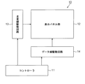
以下、本発明を具体化した第1実施形態を図1〜9に従って説明する。図1は、電気光学装置として有機ELディスプレイ10の回路構成を示すブロック回路図を示す。図2は、表示パネル部の内部回路構成を示すブロック回路図を示す。有機ELディスプレイ10は、制御回路としてのコントローラ11、表示パネル部12、走査線駆動回路13、及びドライバ回路としてのデータ線駆動回路14を備えている。尚、本実施形態における有機ELディスプレイ10は、アクティブマトリクス駆動方式の有機ELディスプレイである。
【0024】
有機ELディスプレイ10のコントローラ11、走査線駆動回路13、及びデータ線駆動回路14は、それぞれが独立した電子部品によって構成されていてもよい。例えば、コントローラ11、走査線駆動回路13、及びデータ線駆動回路14が、各々1チップの半導体集積回路装置によって構成されていてもよい。又、コントローラ11、走査線駆動回路13、及びデータ線駆動回路14の全部若しくは一部がプログラマブルなICチップで構成され、その機能がICチップに書き込まれたプログラムによりソフトウェア的に実現されてもよい。
【0025】
コントローラ11は、表示パネル部12に表示を実行させるための制御信号及びjビット(本実施形態では6ビット)のデジタルデータ(輝度階調データとしての画像データ)を走査線駆動回路13及びデータ線駆動回路14にそれぞれ出力する。尚、本実施形態では、説明の便宜上、画像データは6ビットのデジタル信号である。
【0026】
表示パネル部12は、図2に示すように、複数の画素回路15がマトリクス状に配置された構造を成している。各画素回路15は、その行方向に伸びる複数の走査線Yn(n=1〜N;nは整数)を介して走査線駆動回路13に接続されている。又、各画素回路15は、その列方向に伸びる複数のデータ線Xm(m=1〜M;mは整数)を介してデータ線駆動回路14に接続されている。各画素回路15は、その発光部が有機材料で構成された電気光学素子としての有機EL素子16を有する。
【0027】
画素回路15は、前記データ線駆動回路14から出力される駆動信号としてのデータ線駆動信号の電流Imに応じて有機EL素子16の輝度階調を制御する電流プログラミング方式の画素回路である。詳しくは、画素回路15は、その内部にデータ線駆動回路14から出力されるデータ線駆動信号の電流値に対応した電流値を有する電流を有機EL素子16に供給する電子回路が設けられている。そして、画素回路15は、有機EL素子16に前記データ線駆動信号の電流値に対応した電流が流れることにより有機EL素子16の輝度階調が制御されるようになっている。
【0028】
走査線駆動回路13は、コントローラ11から出力された画像データに基づいて、表示パネル部12に設けられた複数の走査線Ynのうち、1本の走査線を選択し、その選択された走査線に走査線駆動信号を出力する。そして、その走査線駆動信号によって、前記画素回路15の有機EL素子16が発光するタイミングを制御する。
【0029】
データ線駆動回路14は、コントローラ11から出力される6ビットの画像データに基づいてデータ線駆動信号を生成する。詳しくは、データ線駆動回路14は、各データ線Xmとそれぞれ接続した複数の単一ラインドライバ20が備えられている。単一ラインドライバ20は、コントローラ11から出力される画像データに基づいてデータ線駆動信号を生成し、その生成されたデータ線駆動信号をデータ線Xmを介して各画素回路15に出力する。そして、各画素回路15にて、そのデータ線駆動信号の電流Imに対応した電流が有機EL素子16に供給されることで有機EL素子16の輝度階調が制御されるようになっている。尚、本実施形態では、コントローラ11から出力される6ビットの画像データに基づいて、有機EL素子16の輝度階調を64階調制御させるようになっている。
【0030】
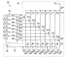
単一ラインドライバ20は、図3に示すように、駆動回路としてのデジタル・アナログ変換回路30と、そのデジタル・アナログ変換回路30の入力側に設けられた電子回路としてのビット拡張回路40とを備えている。
【0031】
デジタル・アナログ変換回路30は、8ビットの電流出力型デジタル・アナログ変換回路である。デジタル・アナログ変換回路30は、アナログ信号線31a〜31hと、8個の第1〜8スイッチングトランジスタ32a〜32hと、8個の第1〜8電流供給用トランジスタ33a〜33hと、デジタル入力信号線34a〜34hとを備えている。
【0032】
アナログ信号線31a〜31hは互いに並列に配列され、アナログ出力端子Poに接続されている。アナログ信号線31a〜31hは、それぞれ、第1〜8スイッチングトランジスタ32a〜32hの各ドレインに接続されている。
【0033】
第1〜8スイッチングトランジスタ32a〜32hは、その各ソースが、第1〜8電流供給用トランジスタ33a〜33hの各ドレインに接続されている。又、第1〜8スイッチングトランジスタ32a〜32hは、その各ゲートが、第1〜8デジタル信号線34a〜34hを介してビット拡張回路40に接続されている。
【0034】
第1〜8電流供給用トランジスタ33a〜33hは、その各ゲートが、それぞれ、電圧供給線35を介して入力端子36に接続されている。そして、各電流供給用トランジスタ33a〜33hは、その入力端子36に基準電圧Voが印加されることによって、それぞれ、所定の電流値を有する電流を出力するようになっている。つまり、第1〜8電流供給用トランジスタ33a〜33hは、それぞれ所定の電流を出力する定電流源として機能するトランジスタである。
【0035】
詳しくは、第1〜8電流供給用トランジスタ33a〜33hは、その利得係数βの相対比が、それぞれ、1:2:4:8:16:32:64:128となるように設定されている。トランジスタの利得係数βは、β=(μCW/L)で定義される。ここで、μはキャリアの移動度、Cはゲート容量、Wはチャネル幅、Lはチャネル長である。従って、各第1〜8電流供給用トランジスタ33a〜33hの電流駆動能力比は、1:2:4:8:16:32:64:128となり、第1〜8電流供給用トランジスタ33a〜33hからそれぞれ出力される電流の大きさIa〜Ihは、以下の関係になる。
【0036】
Ia=Ib/2=Ic/4=Id/8=Ie/16=If/32=Ig/64=Ih/128
又、第1〜8スイッチングトランジスタ32a〜32hのオン・オフ制御は、ビット拡張回路40から出力されるkビットの拡張デジタルデータとしての8ビットのデジタルデータによって行われる。8ビットのデジタルデータの最下位ビットは、利得係数が最も小さな(即ちβの相対値が1の)第1スイッチングトランジスタ32aに供給され、最上位ビットは、利得係数が最も大きな(即ちβの相対値が128の)第8スイッチングトランジスタ32hに出力されるようになっている。
【0037】
デジタル・アナログ変換回路30のアナログ出力端子Poは、前記データ線Xm(m=1〜M)を介して各画素回路15に接続されている。そして、デジタル・アナログ変換回路30は、ビット拡張回路40から出力されるデジタルデータに比例したデータ線駆動信号の電流Imをアナログ出力端子Poから出力する。
【0038】
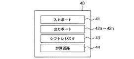
ビット拡張回路40は、図4に示すように、入力ポート41、第1〜8出力ポート42a〜42h、ビットシフト回路としてのシフトレジスタ43、及び、加算回路44を備えている。
【0039】
入力ポート41は、データ線L1〜L6を介してコントローラ11と接続されている。入力ポート41a〜41fは、コントローラ11から出力された6ビットの画像データをデータ線L1〜L6を介してビット拡張回路40にそれぞれ入力させる。
【0040】
第1〜8出力ポート42a〜42hは、第1出力ポート42a、第2出力ポート42b、・・・、第8出力ポート42hの順に、第1デジタル信号線34a、第2デジタル信号線34b、・・・、第8デジタル信号線34hにそれぞれ接続されている。そして、各第1〜8出力ポート42a〜42hは、それぞれ、第1〜8デジタル信号線34a〜34hを介して、第1〜8スイッチングトランジスタ32a〜32hの各ゲートにそれぞれ接続されている。又、第1〜8出力ポート42a〜42hは、第1出力ポート42a、第2出力ポート42b・・・、第8入力ポート42hの順に、後記するシフトレジスタ43及び加算回路44にて演算処理された8ビットのデジタルデータの最下位ビットから最上位ビットの順に対応するように設定されている。尚、本実施形態では、前記デジタルデータは、拡張デジタルデータ及び拡張輝度階調データとしてのデジタルデータである。
【0041】
シフトレジスタ43は、複数の論理回路から構成されたものであって、コントローラ11から出力される6ビットの画像データを8ビットのデジタルデータに拡張するとともにその拡張された8ビットのデジタルデータの各ビットをシフトさせる回路である。
【0042】
加算回路44は、シフトレジスタ43にてシフトされた画像データに所定の8ビットのデータ値を加算させる回路である。
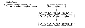
次に、ビット拡張回路40にて行われる演算処理方法を図5〜7に従って説明する。尚、便宜上、コントローラ11から出力される画像データの各ビットの値をhi(i=1〜6)で示すこととする。
【0043】
ビット拡張回路40は、本実施形態では、コントローラ11から出力される6ビットの画像データ(h6,h5,h4,h3,h2,h1)を、以下に示す4つのグループに分けて演算処理を行う。以下、それぞれのグループについて説明する。
【0044】
1.第1グループ
第1グループは、画像データが(0,0,0,0,0,0)〜(0,0,1,1,1,1)である場合(階調1〜16)のグループである。
【0045】
ビット拡張回路40は、そのシフトレジスタ43が6ビットの画像データ(0,0,h4,h3,h2,h1)のうちの下位4ビットを抽出し、その4ビットの上位側にさらに4ビット(0,0,0,0)を付け加え、8ビットの画像データ(0,0,0,0,h4,h3,h2,h1)を生成する(図5参照)。そして、その8ビットの画像データ(0,0,0,0,h4,h3,h2,h1)が、そのまま拡張した8ビットの画像データ(0,0,0,0,b4,b3,b2,b1)として各出力ポート42a〜42hからそれぞれ出力される。
【0046】
2.第2グループ
第2グループは、画像データが(0,1,0,0,0,0)〜(0,1,1,1,1,1)である場合(階調17〜32)のグループである。
【0047】
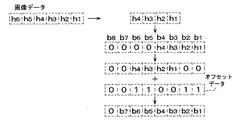
ビット拡張回路40は、そのシフトレジスタ43が6ビットの画像データ(0,h5,h4,h3,h2,h1)のうちの下位4ビットを抽出し、その4ビットの上位側にさらに4ビット(0,0,0,0)を付け加え、8ビットの画像データ(0,0,0,0,h4,h3,h2,h1)を生成する。そして、シフトレジスタ43は、その8ビットの画像データ(0,0,0,0,h4,h3,h2,h1)の下位4ビットの値「h1」〜「h4」を1ビット左にシフトさせ、その最下位ビットを「0」にする(図6参照)。続いて、加算回路44にて、シフトレジスタ43にてシフト処理された8ビットの画像データ(0,0,0,h4,h3,h2,h1,0)に、予め記憶された8ビットのデータ(0,0,0,1,0,0,0,1)を加算させる。前記8ビットのデータ(0,0,0,1,0,0,0,1)はオフセットデータであって、シフトレジスタ43にてシフト処理された8ビットの画像データ(0,0,0,h4,h3,h2,h1,0)の初期値を与えるオフセット値に対応する。つまり、第1グループと第2グループとの連続性を補償するためのデータである。そして,その加算された8ビットのデジタルデータが拡張した8ビットの画像データ[b8(=0),b7(=0),b6,b5,b4,b3,b2,b1(=1)]として各出力ポート42a〜42hからそれぞれ出力される。
【0048】
3.第3グループ
第3グループは、画像データが(1,0,0,0,0,0)〜(1,0,1,1,1,1)である場合(階調33〜48)のグループである。
【0049】
ビット拡張回路40は、そのシフトレジスタ43が6ビットの画像データ(h6,h5,h4,h3,h2,h1)のうちの下位4ビットを抽出し、その4ビットの上位側にさらに4ビット(0,0,0,0)を付け加え、8ビットの画像データ(0,0,0,0,h4,h3,h2,h1)を生成する。そして、シフトレジスタ43にて、その8ビットの画像データ(0,0,0,0,h4,h3,h2,h1)の下位4ビットの値「h1」〜「h4」を2ビット左にシフトさせ、下位2ビットを(0,0)にする(図7参照)。続いて、加算回路44にて、前記シフトレジスタ43にてシフト処理された8ビットの画像データ(0,0,h4,h3,h2,h1,0,0)に、予め記憶された8ビットのデータ(0,0,1,1,0,0,1,1)を加算させる。前記8ビットのデータ(0,0,1,1,0,0,1,1)は、オフセットデータであって、シフトレジスタ43にてシフト処理された8ビットの画像データ(0,0,h4,h3,h2,h1,0,0)の初期値を与えるオフセット値に対応する。つまり、第2グループと第3グループとの連続性を補償するためのデータである。そして,その加算された8ビットのデジタルデータが拡張した8ビットの画像データ[b8(=0),b7,b6,b5,b4,b3,b2(=1),b1(=1)]として各出力ポート42a〜42hからそれぞれ出力される。
【0050】
4.第4グループ
第4グループは、画像データが(1,1,0,0,0,0)〜(1,1,1,1,1,1)である場合(階調49〜64)のグループである。
【0051】
ビット拡張回路40は、そのシフトレジスタ43が6ビットの画像データ(h6,h5,h4,h3,h2,h1)のうちの下位4ビットを抽出し、その4ビットの上位側にさらに4ビット(0,0,0,0)を付け加え、8ビットの画像データ(0,0,0,0,h4,h3,h2,h1)を生成する。そして、シフトレジスタ43にて、その8ビットの画像データ(0,0,0,0,h4,h3,h2,h1)の下位4ビットの値「h1」〜「h4」を3ビット左にシフトさせ、下位3ビットを(0,0,0)にする(図8参照)。続いて、加算回路44にて、前記シフトレジスタ43にてシフト処理された8ビットの画像データ(0,h4,h3,h2,h1,0,0,0)に、予め記憶された8ビットのデータ(0,1,1,1,0,1,1,1)を加算させる。前記8ビットのデータ(0,1,1,1,0,1,1,1)はオフセットデータであって、シフトレジスタ43にてシフト処理された8ビットの画像データ(0,h4,h3,h2,h1,0,0,0)の初期値を与えるオフセット値に対応する。つまり、第3グループと第4グループとの連続性を補償するためのデータである。そして,その加算された8ビットのデジタルデータが拡張した8ビットの画像データ[b8,b7,b6,b5,b4,b3(=1),b2(=1),b1(=1)]として各出力ポート42a〜42hからそれぞれ出力される。ここで、ビット拡張回路40に入力される6ビットの画像データの上位2ビットは、当該6ビットの画像データが第1〜第4のどのグループに属するデータなのかを判別するためのビットとして使用する。
【0052】
尚、前記したようにシフトレジスタ43にて各ビットがシフトされる大きさは、第4のグループへ行くほど大きくなるようにした。このようにすることによって、ビット拡張回路40から出力されるデジタルデータをその値が大きくなるのに従って、高次関数的に急峻に増加させることができる。
【0053】
図9は、コントローラ11から出力される6ビットの画像データに対する、アナログ出力端子Poから出力されるデータ線駆動信号の電流Imを示す。同図より、データ線駆動信号の電流Imを、コントローラ11から出力される画像データが大きくなるのに従って、高次関数的に急峻に増加させることができた。その結果、有機EL素子16の輝度を、その輝度階調が高くなるに従って高次関数的に急峻に増加させることができる。従って、輝度が高い領域においても、人は輝度階調の変化を適確に知覚することができるため、有機ELディスプレイ10の表示品質を向上させることができる。
【0054】
次に、上記のように構成した有機ELディスプレイ10の特徴を以下に記載する。
(1)本実施形態では、コントローラ11から出力される6ビットの画像データに対して、デジタル・アナログ変換回路30から出力されるデータ線駆動信号の電流Imを高次関数的に変化させる8ビットのデジタルデータを生成するビット拡張回路40を構成した。そして、前記ビット拡張回路40をデジタル・アナログ変換回路30の入力側に接続することで単一ラインドライバ20を構成した。その結果、有機EL素子16の輝度を、その輝度階調が高くなるに従って高次関数的に急峻に増加させることができる。このため、輝度が高い領域においても、人は輝度階調の変化を適確に知覚することができるため、有機ELディスプレイ10の表示品質を向上させることができる。
【0055】
(2)本実施形態では、ビット拡張回路40におけるシフト回路をシフトレジスタ43で構成した。従って、複雑な回路を用いなくても、容易にビット拡張回路40を構成することができる。又、シフトレジスタ43を使用することによって、ビット拡張回路40の規模が大きくなることを抑制することができる。
【0056】
(3)本実施形態では、シフトレジスタ43でのビットをシフトさせる大きさは第4グループへ行くほど大きくなるようにした。従って、コントローラ11から出力される画像データが大きくなるのに従って、ビット拡張回路40から出力されるデジタルデータを高次関数的に急峻に増加させることができる。従って、有機ELディスプレイ10の表示品質を向上させることができる。
【0057】
(比較例)
上述の実施形態と比較するために、ビット拡張回路を備えていない単一ラインドライバについて、図13を参照しながら説明する。
【0058】
図13は、前記データ線駆動回路に設けられた6ビット(64階調)の画像データに応じたアナログ電流(駆動電流)を出力する電流出力型デジタル・アナログ変換回路の回路図である。
【0059】
デジタル・アナログ変換回路70は、アナログ出力信号線71a〜71f、スイッチングトランジスタ72a〜72f、電流供給用トランジスタ73a〜73f、及び、デジタル入力信号線74a〜74fを備えている。
【0060】
アナログ出力信号線71a〜71fは、互いに並列に接続され、出力端子76に接続されている。アナログ出力信号線71a〜71fは、対応するスイッチングトランジスタ72a〜72fにそれぞれ接続されている。又、スイッチングトランジスタ72a〜72fは、対応する電流供給用トランジスタ73a〜73fにそれぞれ接続されている。
【0061】
スイッチングトランジスタ72a〜72fの各ゲートは、デジタル入力信号線74a〜74fとそれぞれ接続され、該デジタル入力信号線74a〜74fは図示しないコントローラと接続されている。
【0062】
電流供給用トランジスタ73a〜73fは、それぞれ所定の電流を出力する定電流源として機能するトランジスタである。電流供給用トランジスタ73a〜73fは、その利得係数βの相対比がそれぞれ、1:2:4:8:16:32となるように設定されている。つまり、前記電流供給用トランジスタ73a〜73fから出力される電流値の相対比はそれぞれ、1:2:4:8:16:32となる。
【0063】
第1〜6電流供給用トランジスタ73a〜73fのオン・オフ制御は、前記コントローラから出力される6ビットの画像データによって行われる。6ビットの画像データの最下位ビットは、利得係数βが最も小さな(即ちβの相対値が1の)第1の電流供給用トランジスタ73aに供給され、最上位ビットは、利得係数βが最も大きな(即ちβの相対値が32の)第6電流供給用トランジスタ73fに供給される。そして、コントローラから出力される画像データに応じてスイッチングトランジスタ72a〜72fがオン・オフ制御され、その結果、出力ポート76から前記画像データに応じたアナログ出力電流が出力される。
【0064】
その結果、出力端子76から出力されるアナログ出力電流は、図14に示すように、画像データに対して線形に変化する。従って、前記画素回路では、前記データ線駆動回路から出力されたアナログ出力電流に対応した電流を有機EL素子に供給するので、有機EL素子の輝度階調は、前記画像データに対して線形に変化することとなる。
【0065】
(第2実施形態)
次に、第1実施形態で説明した電気光学装置としての有機ELディスプレイ10の電子機器の適用について図10及び図11に従って説明する。有機ELディスプレイ10は、モバイル型のパーソナルコンピュータ、携帯電話、デジタルカメラ等種々の電子機器に適用できる。
【0066】
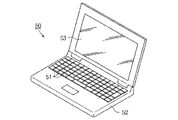
図10は、モバイル型パーソナルコンピュータの構成を示す斜視図を示す。図10において、パーソナルコンピュータ50は、キーボード51を備え本体部52と、前記有機ELディスプレイ10を用いた表示ユニット53を備えている。この場合でも、有機ELディスプレイ10を用いた表示ユニット53は前記実施形態と同様な効果を発揮する。この結果、輝度階調が優れた表示ユニット53を有したモバイル型パーソナルコンピュータ50を提供することができる。
【0067】
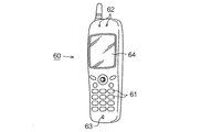
図11は、携帯電話の構成を示す斜視図を示す。図11において、携帯電話60は、複数の操作ボタン61、受話口62、送話口63、前記有機ELディスプレイ10を用いた表示ユニット64を備えている。この場合でも、有機ELディスプレイ10を用いた表示ユニット64は前記実施形態と同様な効果を発揮する。この結果、輝度階調が優れた表示ユニット64を有した携帯電話60を提供することができる。
【0068】
尚、発明の実施形態は、上記実施形態に限定されるものではなく、以下のように実施してもよい。
○上記実施形態では、ビット拡張回路40により拡張されたデジタルデータは電流出力型デジタル・アナログ変換回路に入力されているが、もちろん、電圧出力型デジタル・アナログ変換回路に入力しても同様な効果を奏する。電圧出力型デジタル・アナログ変換回路を用いれば、液晶素子、電気泳動素子、無機EL素子等の電圧駆動型の電気光学素子への適用が可能となる。
【0069】
○上記実施形態では、発光素子として有機EL素子16を用いたが、例えば、LEDやFED、SED(Surface−Conduction Electron−Emitter Device)等のその他の発光素子に適応してもよい。
【0070】
○上記実施形態では、画像データは6ビットあって、デジタル・アナログ変換回路30は8ビットであるとしたが、これに限定されることはなく、任意のビット数を有する画像データ及びデジタル・アナログ変換回路30であってもよい。
【0071】
○上記実施形態では、デジタル・アナログ変換回路30から出力される電流Imが画像データに対して高次関数的に急峻に増加するように、ビット拡張回路40のシフトレジスタ43及び加算回路44でのデータ処理を設定した。このビット拡張回路40のシフトレジスタ43及び加算回路44でのデータ処理を前記データ処理とは異なる他のデータ処理を行うように設定してもよい。たとえば、画像データが(0,0,0,0,0,0)〜(0,0,1,1,1,1)である第1グループでは、前記シフトレジスタ記第1グループの前記画像データのうち、下位4ビットを抽出し、その4ビットの上位側にさらに4ビット(0,0,0,0)を付け加え、8ビットの画像データ(0,0,0,0,h4,h3,h2,h1)を生成する。そして、シフトレジスタ43は、その8ビットの画像データ(0,0,0,0,h4,h3,h2,h1)の下位4ビットの値「h1」〜「h4」を1ビット左にシフトさせ、その最下位ビットを「0」にする。
【0072】
次に、画像データが(0,1,0,0,0,0)〜(0,1,1,1,1,1)である第2グループでは、前記シフトレジスタ43は前記第2グループの前記画像データのうち、下位4ビットを抽出し、その4ビットの上位側にさらに4ビット(0,0,0,0)を付け加え、8ビットの画像データ(0,0,0,0,h4,h3,h2,h1)を生成する。続いて、加算回路44にて、シフトレジスタ43にてシフト処理された8ビットの画像データ(0,0,0,0,h4,h3,h2,h1)に、第1グループと第2グループとの連続性を確保するためのオフセットデータ(0,0,0,1,1,1,1,1)を加算させる。
【0073】
次に、画像データが(1,0,0,0,0,0)〜(1,0,1,1,1,1)である第3グループでは、前記シフトレジスタ43は前記第3グループの前記画像データのうち、下位4ビットを抽出し、その4ビットの上位側にさらに4ビット(0,0,0,0)を付け加え、8ビットの画像データ(0,0,0,0,h4,h3,h2,h1)を生成する。そして、シフトレジスタ43は、その8ビットの画像データ(0,0,0,0,h4,h3,h2,h1)の下位4ビットの値「h1」〜「h4」を1ビット左にシフトさせ、その最下位ビットを「0」にする。続いて、加算回路44にて、シフトレジスタ43にてシフト処理された8ビットの画像データ(0,0,0,h4,h3,h2,h1,0)に、第2グループと第3グループとの連続性を確保するためのオフセットデータ(0,0,1,1,0,0,0,0)を加算させる。
【0074】
次に、画像データが(1,1,0,0,0,0)〜(1,1,1,1,1,1)である第4グループでは、前記シフトレジスタ43は前記第4グループの前記画像データのうち、下位4ビットを抽出し、その4ビットの上位側にさらに4ビット(0,0,0,0)を付け加え、8ビットの画像データ(0,0,0,0,h4,h3,h2,h1)を生成する。続いて、加算回路44にて、シフトレジスタ43にてシフト処理された8ビットの画像データ(0,0,0,0,h4,h3,h2,h1)に、第3グループと第4グループとの連続性を確保するためのオフセットデータ(0,1,0,0,1,1,1,1)を加算させる。
【0075】
このようにすることによって、図12に示すように、画像データの関数としての出力電流が変曲点を有するものとすることができる。
【図面の簡単な説明】
【図1】本実施形態の有機ELディスプレイの回路構成を示すブロック回路図である。
【図2】表示パネル部の内部回路構成を示すブロック回路図である。
【図3】単一ラインドライバを構成するデジタル・アナログ回路及びビット拡張回路の回路図である。
【図4】ビット拡張回路の構成図である。
【図5】ビット拡張回路にて行われる演算処理方法を説明するための図である。
【図6】ビット拡張回路にて行われる演算処理方法を説明するための図である。
【図7】ビット拡張回路にて行われる演算処理方法を説明するための図である。
【図8】ビット拡張回路にて行われる演算処理方法を説明するための図である。
【図9】本実施形態での画像データとデータ線駆動信号の電流値との関係を示す図である。
【図10】第2実施形態を説明するためのモバイル型パーソナルコンピュータの構成を示す斜視図である。
【図11】第2実施形態を説明するための携帯電話の構成を示す斜視図である。
【図12】別例での画像データとデータ線駆動信号の電流値との関係を示す図である。
【図13】電気光学装置で使用されていたデジタル・アナログ変換回路の回路図である。
【図14】画像データとデータ線駆動信号の電流値との関係を示す図である。
【符号の説明】
10 電気光学装置
11 制御回路としてのコントローラ
12 表示パネル部
14 ドライバ回路としてのデータ線駆動回路
15 画素回路
16 電流駆動素子としての有機EL素子
30 駆動回路としてのデジタル・アナログ変換回路
40 電子回路としてのビット拡張回路
43 シフト回路としてのシフトレジスタ
44 補正回路としての加算回路
50,60 電子機器[0001]
TECHNICAL FIELD OF THE INVENTION
The present invention relates to an electronic circuit, an electro-optical device, and an electronic device.
[0002]
[Prior art]
One of the driving methods of an electro-optical device including an electro-optical element such as a liquid crystal element and an organic EL element is an active matrix driving method (for example, see Patent Document 1).
[0003]
[Patent Document 1] Pamphlet of International Publication No. WO98 / 36407
[Problems to be solved by the invention]
By the way, it is known that human vision becomes higher-order functional with respect to luminance gradation. Specifically, human vision drops sharply as the luminance gradation increases. Therefore, even if the luminance gradation of the organic EL element is linearly changed with respect to the image data, it is possible for a person to accurately perceive the change in the luminance gradation of the organic EL element as the luminance gradation increases. Can not. For this reason, when the luminance gradation is linear, the number of gradations to be perceived by a human may be recognized as being smaller than the number of gradations actually output, and as a result, display quality may be reduced. is there.
[0005]
SUMMARY OF THE INVENTION The present invention has been made to solve the above problems, and an object of the present invention is to provide an electronic circuit capable of generating a digital signal having an output value of a predetermined size corresponding to digital data. , Electro-optical device, and electronic equipment.
[0006]
[Means for Solving the Problems]
An electronic circuit according to the present invention includes a shift circuit that converts j-bit (j is a natural number) digital data into k-bit (k is a natural number) digital data, and is electrically connected to the shift circuit. And a correction circuit for continuously changing the k-bit digital data obtained by the shift circuit with the change of the j-bit digital data.
[0007]
According to this, k-bit digital data generated based on j-bit digital data can be arbitrarily changed.
In the electronic circuit, the k-bit digital data is extended digital data that is larger than the j-bit digital data, and the shift circuit divides the range of the j-bit digital data into a plurality of groups. For each group, the digital data is shifted by a predetermined number of bits according to the group and converted to the k-bit digital data.
[0008]
According to this, the j-bit digital data can be converted into k-bit digital data that changes in a higher-order function.
In this electronic circuit, the correction circuit is electrically connected to an electro-optical element, the j-bit digital data is luminance gradation data for controlling the luminance of the electro-optical element, and the k-bit digital data. The data is extended luminance gradation data that gives the amount of analog current supplied to the electro-optical element.
[0009]
According to this, the luminance gradation of the electro-optical element can be arbitrarily changed by j-bit luminance gradation data.
In this electronic circuit, the correction circuit is an addition circuit.
[0010]
According to this, the correction circuit can be easily formed.
In this electronic circuit, the shift circuit determines the number of bits to shift the j-bit digital data according to the size of the j-bit digital data.
[0011]
According to this, k-bit digital data generated based on j-bit digital data can be arbitrarily changed.
In this electronic circuit, the k-bit digital data is extended digital data larger than the j-bit luminance gradation data, and the shift circuit divides the range of the j-bit digital data into a plurality of groups. For each group, the digital data is shifted by a predetermined number of bits according to the group and converted into the k-bit digital data.
[0012]
According to this, the j-bit digital data can be converted into k-bit digital data that changes in a higher-order function.
In this electronic circuit, the shift circuit shifts upward, and the number of bits to be shifted is increased in a group having a larger value.
[0013]
According to this, it is possible to obtain k-bit extended luminance gradation data that increases sharply with respect to the size of the j-bit luminance gradation data.
The electro-optical device according to the present invention includes: a control circuit that outputs j-bit (j is a natural number) luminance gradation data; a driving circuit that generates an analog driving signal based on the j-bit luminance gradation data; A pixel circuit for driving a current driving element based on a driving signal, wherein the driving circuit shifts the j-bit luminance gradation data to convert it into k-bit (k is a natural number) digital data. And a correction circuit electrically connected to the shift circuit for continuously changing the k-bit digital data obtained by the shift circuit with a change in the j-bit luminance gradation data. With.
[0014]
According to this, k-bit digital data generated based on j-bit luminance gradation data can be arbitrarily changed.
In this electro-optical device, the k-bit digital data is extended digital data larger than the j-bit luminance gradation data, and the shift circuit divides the range of the j-bit digital data into a plurality of groups. For each group, the digital data is shifted by a predetermined number of bits according to the group and converted into the k-bit digital data.
[0015]
According to this, the amount of current supplied to the current driving element can be changed in a higher-order function.
In this electro-optical device, the correction circuit is an addition circuit.
[0016]
According to this, the correction circuit of the electro-optical device can be easily formed.
In this electro-optical device, the shift circuit determines the number of bits for bit-shifting the j-bit luminance gradation data according to the size of the j-bit luminance gradation data.
[0017]
According to this, it is possible to realize an electro-optical device capable of controlling the luminance gradation of the current driving element based on the j-bit luminance gradation data.
In this electro-optical device, the shift circuit shifts to a higher order, and the number of bits to be shifted is increased in a group having a larger value.
[0018]
According to this, it is possible to obtain k-bit extended luminance gradation data that increases sharply with respect to the size of the j-bit luminance gradation data. As a result, the electro-optical device can allow a person to accurately perceive the luminance gradation of the current driving element even in a region having a particularly high luminance gradation. Therefore, the display quality of the electro-optical device can be improved.
[0019]
In this electro-optical device, the current driving element is an EL element.
According to this, the luminance gradation of the EL element can be accurately perceived by a person.
[0020]
In this electro-optical device, the EL element has a light-emitting layer made of an organic material.
According to this, the luminance gradation of the organic EL element can be accurately perceived by a person.
[0021]
A first electronic device according to the present invention includes the above electronic circuit.
According to this, it is possible to provide an electronic device having a display unit with excellent luminance gradation.
[0022]
A first electronic device according to the present invention includes the above-described electro-optical device.
According to this, it is possible to provide an electronic device having a display unit with excellent display quality.
[0023]
BEST MODE FOR CARRYING OUT THE INVENTION
(1st Embodiment)
Hereinafter, a first embodiment of the present invention will be described with reference to FIGS. FIG. 1 is a block circuit diagram showing a circuit configuration of an
[0024]
The
[0025]
The
[0026]
The
[0027]
The
[0028]
The scanning
[0029]
The data
[0030]
As shown in FIG. 3, the
[0031]
The digital /
[0032]
The
[0033]
The sources of the first to
[0034]
The gates of the first to eighth current supply transistors 33a to 33h are connected to the
[0035]
Specifically, the first to eighth current supply transistors 33a to 33h are set so that the relative ratio of the gain coefficient β is 1: 2: 4: 8: 16: 32: 64: 128, respectively. . The gain coefficient β of the transistor is defined by β = (μCW / L). Here, μ is the carrier mobility, C is the gate capacitance, W is the channel width, and L is the channel length. Accordingly, the current driving capability ratio of each of the first to eighth current supply transistors 33a to 33h is 1: 2: 4: 8: 16: 32: 64: 128. The magnitudes of the output currents Ia to Ih have the following relationships.
[0036]
Ia = Ib / 2 = Ic / 4 = Id / 8 = Ie / 16 = If / 32 = Ig / 64 = Ih / 128
On / off control of the first to
[0037]
An analog output terminal Po of the digital /
[0038]
As shown in FIG. 4, the
[0039]
The
[0040]
The first to
[0041]
The
[0042]
The
Next, an arithmetic processing method performed by the
[0043]
In the present embodiment, the
[0044]
1. First Group The first group is a group in which image data is (0, 0, 0, 0, 0, 0) to (0, 0, 1, 1, 1, 1) (
[0045]
In the
[0046]
2. The second group is a group in the case where the image data is (0, 1, 0, 0, 0, 0) to (0, 1, 1, 1, 1, 1) (gradations 17 to 32). It is.
[0047]
In the
[0048]
3. Third Group The third group is a group in a case where the image data is (1, 0, 0, 0, 0, 0) to (1, 0, 1, 1, 1, 1) (gradations 33 to 48). It is.
[0049]
In the
[0050]
4. Fourth Group A fourth group is a group (gradation 49 to 64) when the image data is (1,1,0,0,0,0) to (1,1,1,1,1,1,1). It is.
[0051]
In the
[0052]
Note that, as described above, the size by which each bit is shifted by the
[0053]
FIG. 9 shows the current Im of the data line drive signal output from the analog output terminal Po with respect to the 6-bit image data output from the
[0054]
Next, features of the
(1) In the present embodiment, for 6-bit image data output from the
[0055]
(2) In the present embodiment, the shift circuit in the
[0056]
(3) In the present embodiment, the size of shifting the bits in the
[0057]
(Comparative example)
For comparison with the above embodiment, a single line driver without a bit extension circuit will be described with reference to FIG.
[0058]
FIG. 13 is a circuit diagram of a current output type digital / analog conversion circuit provided in the data line driving circuit and outputting an analog current (drive current) corresponding to 6-bit (64 gradation) image data.
[0059]
The digital /
[0060]
The analog
[0061]
The gates of the switching
[0062]
Each of the
[0063]
The on / off control of the first to sixth
[0064]
As a result, the analog output current output from the
[0065]
(2nd Embodiment)
Next, application of the electronic apparatus of the
[0066]
FIG. 10 is a perspective view showing a configuration of a mobile personal computer. In FIG. 10, a
[0067]
FIG. 11 is a perspective view illustrating a configuration of a mobile phone. In FIG. 11, a
[0068]
The embodiments of the present invention are not limited to the above embodiments, but may be implemented as follows.
In the above embodiment, the digital data expanded by the
[0069]
In the above embodiment, the
[0070]
In the above embodiment, the image data has 6 bits and the digital /
[0071]
In the above embodiment, the
[0072]
Next, in the second group in which the image data is (0,1,0,0,0,0) to (0,1,1,1,1,1), the
[0073]
Next, in the third group in which the image data is (1,0,0,0,0,0) to (1,0,1,1,1,1), the
[0074]
Next, in a fourth group in which image data is (1,1,0,0,0,0) to (1,1,1,1,1,1), the
[0075]
In this way, as shown in FIG. 12, the output current as a function of the image data can have an inflection point.
[Brief description of the drawings]
FIG. 1 is a block circuit diagram illustrating a circuit configuration of an organic EL display according to an embodiment.
FIG. 2 is a block circuit diagram showing an internal circuit configuration of a display panel unit.
FIG. 3 is a circuit diagram of a digital / analog circuit and a bit extension circuit constituting a single line driver.
FIG. 4 is a configuration diagram of a bit extension circuit.
FIG. 5 is a diagram for explaining an arithmetic processing method performed by the bit extension circuit.
FIG. 6 is a diagram for explaining an arithmetic processing method performed by the bit extension circuit.
FIG. 7 is a diagram for explaining an arithmetic processing method performed by the bit extension circuit.
FIG. 8 is a diagram for explaining an arithmetic processing method performed by the bit extension circuit.
FIG. 9 is a diagram illustrating a relationship between image data and a current value of a data line drive signal according to the present embodiment.
FIG. 10 is a perspective view showing a configuration of a mobile personal computer for explaining a second embodiment.
FIG. 11 is a perspective view showing a configuration of a mobile phone for explaining a second embodiment.
FIG. 12 is a diagram illustrating a relationship between image data and a current value of a data line drive signal in another example.
FIG. 13 is a circuit diagram of a digital / analog conversion circuit used in the electro-optical device.
FIG. 14 is a diagram illustrating a relationship between image data and a current value of a data line driving signal.
[Explanation of symbols]
Claims (15)
前記シフト回路と電気的に接続し、同シフト回路にて得られた前記kビットのデジタルデータを前記jビットのデジタルデータの変化に伴って連続して変化させるための補正回路と、
を備えたことを特徴とする電子回路。a shift circuit that converts j-bit (j is a natural number) digital data into k-bit (k is a natural number) digital data,
A correction circuit electrically connected to the shift circuit, for continuously changing the k-bit digital data obtained by the shift circuit with a change in the j-bit digital data;
An electronic circuit, comprising:
前記kビットのデジタルデータは、前記jビットのデジタルデータより大きい拡張デジタルデータであり、
前記シフト回路は、前記jビットのデジタルデータの範囲を複数のグループに区分し、各グループ毎にそのデジタルデータをそのグループに応じて予め定められたビット数だけシフトして前記kビットのデジタルデータに変換させるようにしたことを特徴とする電子回路。The electronic circuit according to claim 1,
The k-bit digital data is extended digital data larger than the j-bit digital data,
The shift circuit divides the range of the j-bit digital data into a plurality of groups, shifts the digital data for each group by a predetermined number of bits according to the group, and converts the k-bit digital data into a plurality of groups. An electronic circuit characterized by being converted into.
前記補正回路は電気光学素子と電気的に接続され、
前記jビットのデジタルデータは、前記電気光学素子の輝度を制御するための輝度階調データであり、
前記kビットのデジタルデータは、前記電気光学素子に供給されるアナログ電流の電流量を与える拡張輝度階調データであることを特徴とする電子回路。The electronic circuit according to claim 2,
The correction circuit is electrically connected to the electro-optical element,
The j-bit digital data is luminance gradation data for controlling the luminance of the electro-optical element,
The electronic circuit according to claim 1, wherein the k-bit digital data is extended luminance gradation data that gives a current amount of an analog current supplied to the electro-optical element.
前記補正回路は加算回路であることを特徴とする電子回路。The electronic circuit according to any one of claims 1 to 3,
The electronic circuit, wherein the correction circuit is an addition circuit.
前記シフト回路は、前記jビットのデジタルデータの大きさに応じて、同jビットのデジタルデータをシフトさせるビット数を決定するようにしたことを特徴とする電子回路。The electronic circuit according to any one of claims 1 to 4,
The electronic circuit according to claim 1, wherein the shift circuit determines the number of bits to shift the j-bit digital data according to the size of the j-bit digital data.
前記シフト回路は、上位にシフトするものであり、値が大きいグループほど前記シフトするビット数を大きくするようにしたことを特徴とする電子回路。The electronic circuit according to claim 5,
The electronic circuit, wherein the shift circuit shifts to a higher order, and the number of bits to be shifted is increased in a group having a larger value.
前記jビットの輝度階調データに基づいてアナログ駆動信号を生成する駆動回路と、
前記アナログ駆動信号に基づいて電流駆動素子を駆動させる画素回路とを含み、
前記駆動回路に、
前記jビットの輝度階調データをシフトすることでkビット(kは自然数)のデジタルデータに変換するシフト回路と、
前記シフト回路と電気的に接続し、同シフト回路にて得られた前記kビットのデジタルデータを前記jビットの輝度階調データの変化に伴って連続して変化させるための補正回路と
を備えたことを特徴とする電気光学装置。a control circuit for outputting j-bit (j is a natural number) luminance gradation data;
A drive circuit that generates an analog drive signal based on the j-bit luminance gradation data;
A pixel circuit that drives a current drive element based on the analog drive signal,
In the drive circuit,
A shift circuit that converts the j-bit luminance gradation data into k-bit (k is a natural number) digital data by shifting the j-bit luminance gradation data;
A correction circuit electrically connected to the shift circuit and configured to continuously change the k-bit digital data obtained by the shift circuit with a change in the j-bit luminance gradation data. An electro-optical device, comprising:
前記kビットのデジタルデータは、前記jビットの輝度階調データより大きい拡張デジタルデータであり、
前記シフト回路は、前記jビットのデジタルデータの範囲を複数のグループに区分し、各グループ毎にそのデジタルデータをそのグループに応じて予め定められたビット数だけシフトして前記kビットのデジタルデータに変換させるようにしたことを特徴とする電気光学装置。The electro-optical device according to claim 7,
The k-bit digital data is extended digital data larger than the j-bit luminance gradation data,
The shift circuit divides the range of the j-bit digital data into a plurality of groups, shifts the digital data for each group by a predetermined number of bits according to the group, and converts the k-bit digital data into a plurality of groups. An electro-optical device characterized in that the electro-optical device is converted into an electro-optical device.
前記補正回路は加算回路であることを特徴とする電気光学装置。The electro-optical device according to claim 7, wherein
An electro-optical device, wherein the correction circuit is an addition circuit.
前記シフト回路は、前記jビットの輝度階調データの大きさに応じて、同jビットの輝度階調データをビットシフトさせるビット数を決定するようにしたことを特徴とする電気光学装置。The electro-optical device according to any one of claims 7 to 9,
The electro-optical device according to claim 1, wherein the shift circuit determines the number of bits for bit-shifting the j-bit luminance gradation data according to the size of the j-bit luminance gradation data.
前記シフト回路は、上位にシフトするものであり、値が大きいグループほど前記ビットシフトさせるビット数を大きくするようにしたことを特徴とする電気光学装置。The electro-optical device according to claim 10,
The electro-optical device, wherein the shift circuit shifts to a higher order, and the number of bits to be bit-shifted is increased in a group having a larger value.
前記電流駆動素子は、EL素子であることを特徴とする電気光学装置。The electro-optical device according to any one of claims 7 to 11,
The electro-optical device according to claim 1, wherein the current driving element is an EL element.
前記EL素子は、発光層は有機材料で構成されていることを特徴とする電気光学装置。The electro-optical device according to claim 12,
The electro-optical device according to claim 1, wherein the light emitting layer of the EL element is made of an organic material.
Priority Applications (1)
| Application Number | Priority Date | Filing Date | Title |
|---|---|---|---|
| JP2003198138A JP2004126525A (en) | 2002-07-31 | 2003-07-16 | Electronic circuit, electro-optical device, and electronic apparatus |
Applications Claiming Priority (2)
| Application Number | Priority Date | Filing Date | Title |
|---|---|---|---|
| JP2002223157 | 2002-07-31 | ||
| JP2003198138A JP2004126525A (en) | 2002-07-31 | 2003-07-16 | Electronic circuit, electro-optical device, and electronic apparatus |
Publications (2)
| Publication Number | Publication Date |
|---|---|
| JP2004126525A true JP2004126525A (en) | 2004-04-22 |
| JP2004126525A5 JP2004126525A5 (en) | 2005-10-27 |
Family
ID=32300686
Family Applications (1)
| Application Number | Title | Priority Date | Filing Date |
|---|---|---|---|
| JP2003198138A Pending JP2004126525A (en) | 2002-07-31 | 2003-07-16 | Electronic circuit, electro-optical device, and electronic apparatus |
Country Status (1)
| Country | Link |
|---|---|
| JP (1) | JP2004126525A (en) |
Cited By (1)
| Publication number | Priority date | Publication date | Assignee | Title |
|---|---|---|---|---|
| CN100409304C (en) * | 2004-08-10 | 2008-08-06 | 精工爱普生株式会社 | Impedance conversion circuit, drive circuit, and control method therefor |
-
2003
- 2003-07-16 JP JP2003198138A patent/JP2004126525A/en active Pending
Cited By (1)
| Publication number | Priority date | Publication date | Assignee | Title |
|---|---|---|---|---|
| CN100409304C (en) * | 2004-08-10 | 2008-08-06 | 精工爱普生株式会社 | Impedance conversion circuit, drive circuit, and control method therefor |
Similar Documents
| Publication | Publication Date | Title |
|---|---|---|
| US7486303B2 (en) | Circuit for adjusting gray-scale voltages of a self-emitting display device | |
| US7375711B2 (en) | Electro-optical device, method of driving the same and electronic apparatus | |
| JP4270322B2 (en) | Supplying programming current to the pixel | |
| JP3950988B2 (en) | Driving circuit for active matrix electroluminescent device | |
| KR100670137B1 (en) | Digital/analog converter, display device using the same and display panel and driving method thereof | |
| TWI430230B (en) | Display device | |
| TWI362024B (en) | Driver circuit of amoled with gamma correction | |
| JP2004004788A (en) | Method and circuit for controlling electron device, electronic circuit, electro-optical device, driving method for the same, and electronic equipment | |
| JP2004126523A (en) | Electronic circuit, electro-optical device, and electronic apparatus | |
| WO2004054114A1 (en) | Semiconductor device, digital-analog conversion circuit, and display device using them | |
| US20040155873A1 (en) | Electronic circuit, electro-optical device, method of driving electro-optical device, and electronic apparatus | |
| JP4764493B2 (en) | Semiconductor device and data driver of display device using the same | |
| US20040070578A1 (en) | Electronic circuit, electro-optical device, and electronic apparatus | |
| TWI404000B (en) | Driver for use in flat panel display | |
| JP2004254190A (en) | Electronic circuit, electronic apparatus, electro-optical apparatus and electronic equipment | |
| JP2003233347A (en) | Supply of programming current to pixels | |
| KR20040034393A (en) | Electronics circuit, electro-optic apparatus and electronics instrument | |
| JP2006145926A (en) | Image display device and its driving method | |
| JP2004126525A (en) | Electronic circuit, electro-optical device, and electronic apparatus | |
| JP2004004790A (en) | Method and circuit for controlling electron device, electronic circuit, electro-optical device, driving method for the same, and electronic equipment | |
| JP2004349814A (en) | Digital / analog conversion circuit, electrooptic apparatus, and electronic apparatus | |
| JP2008181081A (en) | Driving device for image display system | |
| JP6739163B2 (en) | Semiconductor device | |
| JP2008256902A (en) | Gradation voltage selection circuit and display control circuit | |
| JP2005079633A (en) | Digital-analog converting circuit, electrooptical apparatus and electronic apparatus |
Legal Events
| Date | Code | Title | Description |
|---|---|---|---|
| A521 | Written amendment |
Free format text: JAPANESE INTERMEDIATE CODE: A523 Effective date: 20050812 |
|
| A621 | Written request for application examination |
Free format text: JAPANESE INTERMEDIATE CODE: A621 Effective date: 20050812 |
|
| A131 | Notification of reasons for refusal |
Free format text: JAPANESE INTERMEDIATE CODE: A131 Effective date: 20060411 |
|
| A521 | Written amendment |
Free format text: JAPANESE INTERMEDIATE CODE: A523 Effective date: 20060609 |
|
| RD04 | Notification of resignation of power of attorney |
Free format text: JAPANESE INTERMEDIATE CODE: A7424 Effective date: 20070403 |
|
| A131 | Notification of reasons for refusal |
Free format text: JAPANESE INTERMEDIATE CODE: A131 Effective date: 20080122 |
|
| A521 | Written amendment |
Free format text: JAPANESE INTERMEDIATE CODE: A523 Effective date: 20080319 |
|
| A02 | Decision of refusal |
Free format text: JAPANESE INTERMEDIATE CODE: A02 Effective date: 20080708 |