JP2004254190A - Electronic circuit, electronic apparatus, electro-optical apparatus and electronic equipment - Google Patents
Electronic circuit, electronic apparatus, electro-optical apparatus and electronic equipment Download PDFInfo
- Publication number
- JP2004254190A JP2004254190A JP2003044351A JP2003044351A JP2004254190A JP 2004254190 A JP2004254190 A JP 2004254190A JP 2003044351 A JP2003044351 A JP 2003044351A JP 2003044351 A JP2003044351 A JP 2003044351A JP 2004254190 A JP2004254190 A JP 2004254190A
- Authority
- JP
- Japan
- Prior art keywords
- transistor
- control terminal
- current
- transistors
- electro
- Prior art date
- Legal status (The legal status is an assumption and is not a legal conclusion. Google has not performed a legal analysis and makes no representation as to the accuracy of the status listed.)
- Pending
Links
- 239000011368 organic material Substances 0.000 claims description 3
- 238000006243 chemical reaction Methods 0.000 abstract description 99
- 239000011159 matrix material Substances 0.000 abstract description 3
- 238000010586 diagram Methods 0.000 description 10
- 230000007274 generation of a signal involved in cell-cell signaling Effects 0.000 description 9
- 239000003990 capacitor Substances 0.000 description 5
- 230000000694 effects Effects 0.000 description 3
- 238000004519 manufacturing process Methods 0.000 description 2
- 239000003086 colorant Substances 0.000 description 1
- 239000004065 semiconductor Substances 0.000 description 1
Images


Classifications
-
- G—PHYSICS
- G09—EDUCATION; CRYPTOGRAPHY; DISPLAY; ADVERTISING; SEALS
- G09G—ARRANGEMENTS OR CIRCUITS FOR CONTROL OF INDICATING DEVICES USING STATIC MEANS TO PRESENT VARIABLE INFORMATION
- G09G3/00—Control arrangements or circuits, of interest only in connection with visual indicators other than cathode-ray tubes
- G09G3/20—Control arrangements or circuits, of interest only in connection with visual indicators other than cathode-ray tubes for presentation of an assembly of a number of characters, e.g. a page, by composing the assembly by combination of individual elements arranged in a matrix no fixed position being assigned to or needed to be assigned to the individual characters or partial characters
- G09G3/22—Control arrangements or circuits, of interest only in connection with visual indicators other than cathode-ray tubes for presentation of an assembly of a number of characters, e.g. a page, by composing the assembly by combination of individual elements arranged in a matrix no fixed position being assigned to or needed to be assigned to the individual characters or partial characters using controlled light sources
- G09G3/30—Control arrangements or circuits, of interest only in connection with visual indicators other than cathode-ray tubes for presentation of an assembly of a number of characters, e.g. a page, by composing the assembly by combination of individual elements arranged in a matrix no fixed position being assigned to or needed to be assigned to the individual characters or partial characters using controlled light sources using electroluminescent panels
- G09G3/32—Control arrangements or circuits, of interest only in connection with visual indicators other than cathode-ray tubes for presentation of an assembly of a number of characters, e.g. a page, by composing the assembly by combination of individual elements arranged in a matrix no fixed position being assigned to or needed to be assigned to the individual characters or partial characters using controlled light sources using electroluminescent panels semiconductive, e.g. using light-emitting diodes [LED]
- G09G3/3208—Control arrangements or circuits, of interest only in connection with visual indicators other than cathode-ray tubes for presentation of an assembly of a number of characters, e.g. a page, by composing the assembly by combination of individual elements arranged in a matrix no fixed position being assigned to or needed to be assigned to the individual characters or partial characters using controlled light sources using electroluminescent panels semiconductive, e.g. using light-emitting diodes [LED] organic, e.g. using organic light-emitting diodes [OLED]
- G09G3/3225—Control arrangements or circuits, of interest only in connection with visual indicators other than cathode-ray tubes for presentation of an assembly of a number of characters, e.g. a page, by composing the assembly by combination of individual elements arranged in a matrix no fixed position being assigned to or needed to be assigned to the individual characters or partial characters using controlled light sources using electroluminescent panels semiconductive, e.g. using light-emitting diodes [LED] organic, e.g. using organic light-emitting diodes [OLED] using an active matrix
- G09G3/3233—Control arrangements or circuits, of interest only in connection with visual indicators other than cathode-ray tubes for presentation of an assembly of a number of characters, e.g. a page, by composing the assembly by combination of individual elements arranged in a matrix no fixed position being assigned to or needed to be assigned to the individual characters or partial characters using controlled light sources using electroluminescent panels semiconductive, e.g. using light-emitting diodes [LED] organic, e.g. using organic light-emitting diodes [OLED] using an active matrix with pixel circuitry controlling the current through the light-emitting element
- G09G3/3241—Control arrangements or circuits, of interest only in connection with visual indicators other than cathode-ray tubes for presentation of an assembly of a number of characters, e.g. a page, by composing the assembly by combination of individual elements arranged in a matrix no fixed position being assigned to or needed to be assigned to the individual characters or partial characters using controlled light sources using electroluminescent panels semiconductive, e.g. using light-emitting diodes [LED] organic, e.g. using organic light-emitting diodes [OLED] using an active matrix with pixel circuitry controlling the current through the light-emitting element the current through the light-emitting element being set using a data current provided by the data driver, e.g. by using a two-transistor current mirror
-
- F—MECHANICAL ENGINEERING; LIGHTING; HEATING; WEAPONS; BLASTING
- F16—ENGINEERING ELEMENTS AND UNITS; GENERAL MEASURES FOR PRODUCING AND MAINTAINING EFFECTIVE FUNCTIONING OF MACHINES OR INSTALLATIONS; THERMAL INSULATION IN GENERAL
- F16K—VALVES; TAPS; COCKS; ACTUATING-FLOATS; DEVICES FOR VENTING OR AERATING
- F16K19/00—Arrangements of valves and flow lines specially adapted for mixing fluids
- F16K19/006—Specially adapted for faucets
-
- F—MECHANICAL ENGINEERING; LIGHTING; HEATING; WEAPONS; BLASTING
- F16—ENGINEERING ELEMENTS AND UNITS; GENERAL MEASURES FOR PRODUCING AND MAINTAINING EFFECTIVE FUNCTIONING OF MACHINES OR INSTALLATIONS; THERMAL INSULATION IN GENERAL
- F16K—VALVES; TAPS; COCKS; ACTUATING-FLOATS; DEVICES FOR VENTING OR AERATING
- F16K27/00—Construction of housing; Use of materials therefor
- F16K27/02—Construction of housing; Use of materials therefor of lift valves
-
- F—MECHANICAL ENGINEERING; LIGHTING; HEATING; WEAPONS; BLASTING
- F16—ENGINEERING ELEMENTS AND UNITS; GENERAL MEASURES FOR PRODUCING AND MAINTAINING EFFECTIVE FUNCTIONING OF MACHINES OR INSTALLATIONS; THERMAL INSULATION IN GENERAL
- F16K—VALVES; TAPS; COCKS; ACTUATING-FLOATS; DEVICES FOR VENTING OR AERATING
- F16K31/00—Actuating devices; Operating means; Releasing devices
- F16K31/44—Mechanical actuating means
- F16K31/60—Handles
-
- G—PHYSICS
- G09—EDUCATION; CRYPTOGRAPHY; DISPLAY; ADVERTISING; SEALS
- G09G—ARRANGEMENTS OR CIRCUITS FOR CONTROL OF INDICATING DEVICES USING STATIC MEANS TO PRESENT VARIABLE INFORMATION
- G09G3/00—Control arrangements or circuits, of interest only in connection with visual indicators other than cathode-ray tubes
- G09G3/20—Control arrangements or circuits, of interest only in connection with visual indicators other than cathode-ray tubes for presentation of an assembly of a number of characters, e.g. a page, by composing the assembly by combination of individual elements arranged in a matrix no fixed position being assigned to or needed to be assigned to the individual characters or partial characters
- G09G3/22—Control arrangements or circuits, of interest only in connection with visual indicators other than cathode-ray tubes for presentation of an assembly of a number of characters, e.g. a page, by composing the assembly by combination of individual elements arranged in a matrix no fixed position being assigned to or needed to be assigned to the individual characters or partial characters using controlled light sources
- G09G3/30—Control arrangements or circuits, of interest only in connection with visual indicators other than cathode-ray tubes for presentation of an assembly of a number of characters, e.g. a page, by composing the assembly by combination of individual elements arranged in a matrix no fixed position being assigned to or needed to be assigned to the individual characters or partial characters using controlled light sources using electroluminescent panels
- G09G3/32—Control arrangements or circuits, of interest only in connection with visual indicators other than cathode-ray tubes for presentation of an assembly of a number of characters, e.g. a page, by composing the assembly by combination of individual elements arranged in a matrix no fixed position being assigned to or needed to be assigned to the individual characters or partial characters using controlled light sources using electroluminescent panels semiconductive, e.g. using light-emitting diodes [LED]
- G09G3/3208—Control arrangements or circuits, of interest only in connection with visual indicators other than cathode-ray tubes for presentation of an assembly of a number of characters, e.g. a page, by composing the assembly by combination of individual elements arranged in a matrix no fixed position being assigned to or needed to be assigned to the individual characters or partial characters using controlled light sources using electroluminescent panels semiconductive, e.g. using light-emitting diodes [LED] organic, e.g. using organic light-emitting diodes [OLED]
- G09G3/3275—Details of drivers for data electrodes
- G09G3/3283—Details of drivers for data electrodes in which the data driver supplies a variable data current for setting the current through, or the voltage across, the light-emitting elements
-
- G—PHYSICS
- G09—EDUCATION; CRYPTOGRAPHY; DISPLAY; ADVERTISING; SEALS
- G09G—ARRANGEMENTS OR CIRCUITS FOR CONTROL OF INDICATING DEVICES USING STATIC MEANS TO PRESENT VARIABLE INFORMATION
- G09G2300/00—Aspects of the constitution of display devices
- G09G2300/08—Active matrix structure, i.e. with use of active elements, inclusive of non-linear two terminal elements, in the pixels together with light emitting or modulating elements
- G09G2300/0809—Several active elements per pixel in active matrix panels
- G09G2300/0842—Several active elements per pixel in active matrix panels forming a memory circuit, e.g. a dynamic memory with one capacitor
-
- G—PHYSICS
- G09—EDUCATION; CRYPTOGRAPHY; DISPLAY; ADVERTISING; SEALS
- G09G—ARRANGEMENTS OR CIRCUITS FOR CONTROL OF INDICATING DEVICES USING STATIC MEANS TO PRESENT VARIABLE INFORMATION
- G09G2310/00—Command of the display device
- G09G2310/02—Addressing, scanning or driving the display screen or processing steps related thereto
- G09G2310/0262—The addressing of the pixel, in a display other than an active matrix LCD, involving the control of two or more scan electrodes or two or more data electrodes, e.g. pixel voltage dependent on signals of two data electrodes
-
- G—PHYSICS
- G09—EDUCATION; CRYPTOGRAPHY; DISPLAY; ADVERTISING; SEALS
- G09G—ARRANGEMENTS OR CIRCUITS FOR CONTROL OF INDICATING DEVICES USING STATIC MEANS TO PRESENT VARIABLE INFORMATION
- G09G2310/00—Command of the display device
- G09G2310/02—Addressing, scanning or driving the display screen or processing steps related thereto
- G09G2310/0264—Details of driving circuits
- G09G2310/027—Details of drivers for data electrodes, the drivers handling digital grey scale data, e.g. use of D/A converters
-
- G—PHYSICS
- G09—EDUCATION; CRYPTOGRAPHY; DISPLAY; ADVERTISING; SEALS
- G09G—ARRANGEMENTS OR CIRCUITS FOR CONTROL OF INDICATING DEVICES USING STATIC MEANS TO PRESENT VARIABLE INFORMATION
- G09G2330/00—Aspects of power supply; Aspects of display protection and defect management
- G09G2330/02—Details of power systems and of start or stop of display operation
- G09G2330/028—Generation of voltages supplied to electrode drivers in a matrix display other than LCD
Abstract
Description
【0001】
【発明の属する技術分野】
本発明は、電子回路、電子装置、電気光学装置及び電子機器に関するものである。
【0002】
【従来の技術】
有機EL素子を用いた表示装置の一つに、画素回路毎に有機EL素子を制御する駆動トランジスタを備えたアクティブマトリクス型表示装置がある。
【0003】
この種の表示装置は、デジタルデータである画像データに応じたデータ電流をデータ線を介して前記画素回路に出力するデータ線駆動回路を備えている。このデータ線駆動回路は、その内部に複数のデジタル・アナログ変換回路を備えた単一ラインドライバを有しており、そのデジタル・アナログ変換回路にて前記画像データをアナログ信号に変換した後にデータ線を介して各画素回路に出力する(例えば、特許文献1)。
【0004】
【特許文献1】
特開2000−122608号公報
【0005】
【発明が解決しようとする課題】
ところで、一般に画素回路の数は非常に多く、そのため、複数の単一ラインドライバを互いに電気的に接続して一つのデータ線駆動回路を形成する場合がある。しかしながら、各単一ラインドライバは、そのデジタル・アナログ変換回路を構成するトランジスタの特性ばらつきによって、同じ画像データに対して異なった大きさのデータ電流がそれぞれ出力されてしまう。その結果、有機EL素子は、同じ画像データに対して、接続された単一ラインドライバによって異なった輝度で発光することとなる。このことによって、表示品位が優れた電気光学装置を提供することができない。
【0006】
本発明は上記問題点を解消するためになされたものであって、その目的は、トランジスタの特性ばらつきを抑制することができる電子装置、電気光学装置及び電子機器を提供することにある。
【0007】
【課題を解決するための手段】
本発明における電子回路は、第1の制御用端子を備えた、ダイオード接続された第1のトランジスタと、第2の制御用端子を備え、前記第1の制御用端子に前記第2の制御用端子が接続された複数の第2のトランジスタと、各々が信号線に接続された第3の制御用端子を備え、前記複数の第2のトランジスタの各々に直列に接続された複数の第3のトランジスタと、第4の制御用端子を備え、前記第1の制御用端子に前記第4の制御用端子が接続された第4のトランジスタと、を含み、前記複数の第3のトランジスタのうち、前記信号線を介して供給されるオン信号によりオン状態とされた第3のトランジスタと、前記複数の第2のトランジスタのうち、前記オン状態とされた第3のトランジスタと直列に接続された第2のトランジスタと、からなる電流経路は一つの出力端子に接続され、前記第4のトランジスタは前記一つの出力端子には接続されない。
【0008】
これによれば、信号線を介して第3トランジスタに供給するデジタルデータに応じた大きさのアナログ電流を出力するデジタル・アナログ変換回路を構成するとともに、前記アナログ電流とは関係がない第1のトランジスタを基準値とした電流を出力する電子回路を提供することができる。
【0009】
この電子回路において、前記第4のトランジスタの利得係数は、前記第1のトランジスタの利得係数と同じであってもよい。
これによれば、第4のトランジスタから出力されるアナログ電流の電流レベルは、第1のトランジスタを流れる電流の電流レベルと同じにすることができる。
【0010】
この電子回路において、第5の制御用端子を備え、前記第1のトランジスタと直列に接続された第5のトランジスタと、第6の制御用端子を備え、前記第5の制御用端子が前記第6の制御用端子に接続された、ダイオード接続された第6のトランジスタとを備えていてもよい。
これによれば、第1の制御用端子に生じる電圧の電圧レベルを第6のトランジスタに流れる電流の電流レベルで制御することができる。
【0011】
本発明の電子回路は、第1の制御用端子を備えた、ダイオード接続された第1のトランジスタと、前記第1の制御用端子の電圧レベルを基準値とした電流を出力する複数の第2のトランジスタと、各々が第3の制御用端子を備え、前記第3の制御用端子に入力されるオン・オフ信号に応じて前記複数の第2のトランジスタの各々から出力される電流を制御する第3のトランジスタと、第4の制御用端子を備え、前記第1の制御用端子の電圧レベルを基準値とした電流を出力する第4のトランジスタと、を含み、前記第4のトランジスタから出力される電流は、前記複数の第2のトランジスタの各々から出力される電流経路には流れないようにした。
【0012】
これによれば、信号線を介して第3トランジスタに供給するデジタルデータに応じた大きさのアナログ電流を出力するデジタル・アナログ変換回路を構成するとともに、前記アナログ電流とは関係がない第1のトランジスタを基準値とした電流を出力する電子回路を提供することができる。
【0013】
本発明の電子回路は、第1の制御用端子を備えた、ダイオード接続された第1のトランジスタと、前記第1の制御用端子の電圧レベルを基準値とした電流を出力する複数の第2のトランジスタと、各々が第3の制御用端子を備え、前記第3の制御用端子に入力されるオン・オフ信号に応じて前記複数の第2のトランジスタの各々から出力される電流を制御する第3のトランジスタと、前記第1の制御用端子の電圧レベルを基準値とした電流を出力する第4のトランジスタと、を含み、前記複数の第3のトランジスタのうち、前記オン・オフ信号によりオン状態とされた第3のトランジスタと、前記複数の第2のトランジスタのうち、前記オン状態とされた第3のトランジスタと直列に接続された第2のトランジスタと、からなる電流経路には、前記第4のトランジスタは設けられていない。
【0014】
これによれば、信号線を介して第3トランジスタに供給するデジタルデータに応じた大きさのアナログ電流を出力するデジタル・アナログ変換回路を構成するとともに、前記アナログ電流とは関係がない第1のトランジスタを基準値とした電流を出力する電子回路を提供することができる。
【0015】
この電子回路において、前記第4のトランジスタの利得係数は、前記第1のトランジスタの利得係数と同じであってもよい。
これによれば、第4のトランジスタから出力されるアナログ電流の電流レベルは、第1のトランジスタを流れる電流の電流レベルと同じにすることができる。
【0016】
この電子回路において、第5の制御用端子を備え、前記第1のトランジスタと直列に接続された第5のトランジスタと、第6の制御用端子を備え、前記第5の制御用端子が前記第6の制御用端子に接続された、ダイオード接続された第6のトランジスタとを備えていてもよい。
これによれば、第1の制御用端子に生じる電圧の電圧レベルを第6のトランジスタに流れる電流の電流レベルで制御することができる。
【0017】
本発明の電子装置は、複数の単位回路を備えた電子装置において、前記複数の単位回路の各々は、第1の制御用端子を備えた、ダイオード接続された第1のトランジスタと、第2の制御用端子を備え、前記第1の制御用端子に前記第2の制御用端子が接続された複数の第2のトランジスタと、各々が信号線に接続された第3の制御用端子を備え、前記複数の第2のトランジスタの各々に直列に接続された複数の第3のトランジスタと、第4の制御用端子を備え、前記第1の制御用端子に前記第4の制御用端子が接続されるとともに、前記信号線を介して供給されるオン信号によりオン状態とされた前記第3のトランジスタと直列に接続された第2のトランジスタからなる電流経路には設けられていない第4のトランジスタと、を含み、前記第4のトランジスタは、接続線を介して他の単位回路に接続され、前記第4のトランジスタから出力される電流レベルに応じて、他の単位回路に含まれる第1の制御用端子の電圧レベルを制御する。
【0018】
これによれば、1つの単位回路にて生成される電流を基準電流とし、その基準電流を他の各単位回路の第1のトランジスに供給する。そして、その基準電流に応じて他の各単位回路の第1のトランジスタの第1の制御用端子の電圧を制御する。第1のトランジスタは、この基準電流を基準値として駆動するので、単位回路間の前記第1のトランジスタの閾値電圧といった特性ばらつきによるを抑制することができる。その結果、各単位回路は、その各第3のトランジスタに入力されるオン・オフ信号に応じた電流を精度良く出力することができる。
【0019】
この電子装置において、前記複数の単位回路の各々の前記第4のトランジスタの利得係数は、前記第1のトランジスタの利得係数と同じであってもよい。
これによれば、1つの単位回路の第1のトランジスタに流れる電流の電流レベルを他の単位回路の全ての第1のトランジスタに流れる電流の電流レベルと同じにすることができる。
【0020】
この電子装置において、前記複数の単位回路の各々は、第5の制御用端子を備え、前記第1のトランジスタと直列に接続された第5のトランジスタと、第6の制御用端子を備え、前記第5の制御用端子が前記第6の制御用端子に接続された、ダイオード接続された第6のトランジスタとを備えていてもよい。
これによれば、第1の制御用端子に生じる電圧の電圧レベルを第6のトランジスタに流れる電流の電流レベルで制御することができる。
【0021】
本発明の電子装置は、複数の単位回路を備えた電子装置において、前記複数の単位回路の各々は、第1の制御用端子を備えた、ダイオード接続された第1のトランジスタと、前記第1の制御用端子の電圧レベルを基準値とした電流を出力する複数の第2のトランジスタと、各々が第3の制御用端子を備え、前記第3の制御用端子に入力されるオン・オフ信号に応じて前記複数の第2のトランジスタの各々から出力される電流を制御する第3のトランジスタと、第4の制御用端子を備え、前記第1の制御用端子の電圧レベルを基準値とした電流を出力する第4のトランジスタと、を含み、前記第4のトランジスタから出力される電流は、前記オン・オフ信号によりオン状態とされた前記第3のトランジスタと直列に接続された第2のトランジスタからなる電流経路には供給されず、他の単位回路に供給される。
【0022】
これによれば、各単位回路は、各第3のトランジスタに入力されるオン・オフ信号に応じた電流レベルを有するアナログ電流を出力するととも、第4のトランジスタからは前記アナログ電流と関係なく独立した電流を他の単位回路に供給する。そして、他の各単位回路は、前記第4のトランジスタから出力された電流を基準電流として各単位回路に含まれる第1のトランジスタの第1の制御用端子の電圧を設定する。このことによって、前記単位回路の各々は、その第1のトランジスタの特性にバラツキを抑制することができる。従って、各単位回路から出力されるアナログ電流を精度良く制御することができる。
【0023】
本発明の電子装置は、複数の単位回路を備えた電子装置において、前記複数の単位回路の各々は、第1の制御用端子を備えた、ダイオード接続された第1のトランジスタと、前記第1の制御用端子の電圧レベルを基準値とした電流を出力する複数の第2のトランジスタと、各々が第3の制御用端子を備え、前記第3の制御用端子に入力されるオン・オフ信号に応じて前記複数の第2のトランジスタの各々から出力される電流を制御する第3のトランジスタと、第4の制御用端子を備え、前記第1の制御用端子の電圧レベルを基準値とした電流を出力する第4のトランジスタと、を含み、前記第4のトランジスタから出力される電流は、他の単位回路の第1の制御用端子の電圧レベルを設定する基準電流となる。
【0024】
これによれば、各単位回路は、各第3のトランジスタに入力されるオン・オフ信号に応じた電流レベルを有するアナログ電流を出力するととも、第4のトランジスタからは前記アナログ電流と関係なく独立した電流を他の単位回路に供給する。そして、他の各単位回路は、前記第4のトランジスタから出力された電流を基準電流として各単位回路に含まれる第1のトランジスタの第1の制御用端子の電圧を設定する。このことによって、前記単位回路の各々は、その第1のトランジスタの特性にバラツキを抑制することができる。従って、各単位回路から出力されるアナログ電流を精度良く制御することができる。
【0025】
この電子装置において、前記複数の単位回路の各々の前記第4のトランジスタの利得係数は、前記第1のトランジスタの利得係数と同じであってもよい。
これによれば、1つの単位回路の第1のトランジスタに流れる電流の電流レベルを他の単位回路の全ての基準電流とする。
【0026】
この電子装置において、複数の前記単位回路は、カスケード接続されていてもよい。
これによれば、カスケード接続された単位回路にて生成されるアナログ電流を前記第3の制御用端子に入力されるオン・オフ信号に応じて精度良く制御することができる。
【0027】
この電子装置において、前記複数の単位回路の各々は、第5の制御用端子を備え、前記第1のトランジスタと直列に接続された第5のトランジスタと、第6の制御用端子を備え、前記第5の制御用端子が前記第6の制御用端子に接続された、ダイオード接続された第6のトランジスタとが設けられていもよい。
【0028】
これによれば、第1の制御用端子に生じる電圧の電圧レベルを第6のトランジスタに流れる電流の電流レベルで制御することができる。
本発明の電子装置は、複数の単位回路を備えた電子装置において、前記複数の単位回路の各々は、第1の制御用端子を備えた、ダイオード接続された第1のトランジスタと、前記第1の制御用端子の電圧レベルを基準値とした電流を出力する複数の第2のトランジスタと、各々が第3の制御用端子を備え、前記第3の制御用端子に入力されるオン・オフ信号に応じて前記複数の第2のトランジスタの各々から出力される電流を制御する第3のトランジスタと、第4の制御用端子を備え、前記第1の制御用端子の電圧レベルを基準値とした電流を出力する第4のトランジスタと、第5の制御用端子を備え、前記第1のトランジスタと直列に接続された第5のトランジスタと、第6の制御用端子を備え、前記第5の制御用端子が前記第6の制御用端子に接続された、ダイオード接続された第6のトランジスタと、を含み、前記第4のトランジスタは、同第4のトランジスタが含まれる単位回路の、前記オン・オフ信号によりオン状態とされた前記第3のトランジスタと直列に接続された第2のトランジスタとは接続されず、他の単位回路に含まれる前記第6のトランジスタに接続されている。
【0029】
これによれば、各単位回路は、各第3のトランジスタに入力されるオン・オフ信号に応じた電流レベルを有するアナログ電流を出力するととも、第4のトランジスタからは前記アナログ電流と関係なく独立した電流を他の単位回路に供給する。そして、他の各単位回路は、前記第4のトランジスタから出力された電流を基準電流として各単位回路に含まれる第6のトランジスタに供給される。そして、第6のトランジスタを流れる基準電流によって第1のトランジスタの第1の制御用端子の電圧を設定する。このことによって、前記単位回路の各々は、その第1のトランジスタの特性にバラツキを抑制することができる。従って、各単位回路から出力されるアナログ電流を精度良く制御することができる。
【0030】
この電子装置において、前記複数の単位回路の各々の前記第4のトランジスタの利得係数は、前記第1のトランジスタの利得係数と同じであってもよい。
これによれば、1つの単位回路の第1のトランジスタに流れる電流の電流レベルを他の単位回路の全ての第1のトランジスタに流れる電流の電流レベルと同じにすることができる。
【0031】
この電子装置において、複数の前記単位回路は、カスケード接続されていてもよい。
これによれば、カスケード接続された単位回路にて生成されるアナログ電流を前記第3の制御用端子に入力されるオン・オフ信号に応じて精度良く制御することができる。
【0032】
本発明の電気光学装置は、複数の走査線と、複数のデータ線と、これら各前記走査線と各前記データ線との交差部に対応してそれぞれ配設された電気光学素子とを備えるとともに、各前記データ線にデータ電流を供給するデータ電流供給回路を備え、各前記電気光学素子に前記データ電流に応じた駆動電流量を供給する電気光学装置において、前記データ電流供給回路は、第1の制御用端子を備えた、ダイオード接続された第1のトランジスタと、第2の制御用端子を備え、前記第1の制御用端子に前記第2の制御用端子が接続された複数の第2のトランジスタと、各々が画像データを供給する信号線に接続された第3の制御用端子を備え、前記複数の第2のトランジスタの各々と直列に接続された複数の第3のトランジスタと、第4の制御用端子を備え、前記第1の制御用端子に前記第4の制御用端子が接続された第4のトランジスタとを含み、前記第4のトランジスタは、接続線を介して他のデータ電流供給回路に接続され、前記第4のトランジスタから出力される電流レベルに応じて、他のデータ電流供給回路に含まれる第1の制御用端子の電圧レベルを制御する。
【0033】
これによれば、画像データに応じた大きさのアナログ電流を出力するデジタル・アナログ変換回路を構成するとともに、前記アナログ電流とは関係がない第1のトランジスタを基準値とした電流を出力することができる。このことによって、各単位回路の第1のトランジスタの特性バラツキを抑制することができるので、前記画像データに応じた大きさのアナログ電流を精度良く出力することができる。その結果、優れた表示品位を備えた電気光学装置を提供することができる。
【0034】
この電気光学装置において、前記第4のトランジスタの利得係数は、前記第1のトランジスタの利得係数と同じであってもよい。
これによれば、1つの単位回路の第1のトランジスタに流れる電流の電流レベルを他の単位回路の全ての第1のトランジスタに流れる電流の電流レベルと同じにすることができる。
【0035】
この電気光学装置において、前記データ電流供給回路は、第5の制御用端子を備え、前記第1のトランジスタと直列に接続された第5のトランジスタと、第6の制御用端子を備え、前記第5の制御用端子が前記第6の制御用端子に接続された、ダイオード接続された第6のトランジスタとを備えていてもよい。
【0036】
これによれば、第1の制御用端子に生じる電圧の電圧レベルを第6のトランジスタに流れる電流の電流レベルで制御することができる。
本発明の電気光学装置は、複数の走査線と、複数のデータ線と、これら各前記走査線と各前記データ線との交差部に対応してそれぞれ配設された電気光学素子とを備えるとともに、各前記データ線にデータ電流を供給するデータ電流供給回路を備え、各前記電気光学素子に前記データ電流に応じた駆動電流量を供給する電気光学装置において、前記各データ電流供給回路は、第1の制御用端子を備えた、ダイオード接続された第1のトランジスタと、前記第1の制御用端子の電圧レベルを基準値とした電流を出力する複数の第2のトランジスタと、各々が第3の制御用端子を備え、前記第3の制御用端子に入力される画像データに応じて前記複数の第2のトランジスタの各々から出力される電流を制御する第3のトランジスタと、第4の制御用端子を備え、前記第1の制御用端子の電圧レベルを基準値とした電流を出力する第4のトランジスタと、を含み、前記第4のトランジスタから出力される電流は、前記画像データによりオン状態とされた前記第3のトランジスタと直列に接続された第2のトランジスタからなる電流経路には供給されず、他の単位回路に供給される。
【0037】
これによれば、各単位回路は、各第3のトランジスタに入力されるオン・オフ信号に応じた電流レベルを有するアナログ電流を出力するととも、第4のトランジスタからは前記アナログ電流と関係なく独立した電流を他の単位回路に供給する。そして、他の各単位回路は、前記第4のトランジスタから出力された電流を基準電流として各単位回路に含まれる第1のトランジスタの第1の制御用端子の電圧を設定する。このことによって、前記単位回路の各々は、その第1のトランジスタの特性にバラツキを抑制することができる。従って、各単位回路から出力されるアナログ電流を精度良く制御することができる。この結果、優れた表示品位を備えた電気光学装置を提供することができる。
【0038】
本発明の電気光学装置は、複数の走査線と、複数のデータ線と、これら各前記走査線と各前記データ線との交差部に対応してそれぞれ配設された電気光学素子とを備えるとともに、各前記データ線にデータ電流を供給するデータ電流供給回路を備え、各前記電気光学素子に前記データ電流に応じた駆動電流量を供給する電気光学装置において、前記各データ電流供給回路は、第1の制御用端子を備えた、ダイオード接続された第1のトランジスタと、前記第1の制御用端子の電圧レベルを基準値とした電流を出力する複数の第2のトランジスタと、各々が第3の制御用端子を備え、前記第3の制御用端子に入力される画像データに応じて前記複数の第2のトランジスタの各々から出力される電流を制御する第3のトランジスタと、第4の制御用端子を備え、前記第1の制御用端子の電圧レベルを基準値とした電流を出力する第4のトランジスタと、を含み、前記第4のトランジスタから出力される電流は、他の単位回路の第1の制御用端子の電圧レベルを設定する基準電流となる。
【0039】
これによれば、各単位回路は、各第3のトランジスタに入力されるオン・オフ信号に応じた電流レベルを有するアナログ電流を出力するととも、第4のトランジスタからは前記アナログ電流と関係なく独立した電流を他の単位回路に供給する。そして、他の各単位回路は、前記第4のトランジスタから出力された電流を基準電流として各単位回路に含まれる第1のトランジスタの第1の制御用端子の電圧を設定する。このことによって、前記単位回路の各々は、その第1のトランジスタの特性にバラツキを抑制することができる。従って、各単位回路から出力されるアナログ電流を精度良く制御することができる。この結果、優れた表示品位を備えた電気光学装置を提供することができる。
【0040】
この電気光学装置において、前記複数のデータ電流供給回路の各々の前記第4のトランジスタの利得係数は、前記第1のトランジスタの利得係数と同じであってもよい。
これによれば、1つの単位回路の第1のトランジスタに流れる電流の電流レベルを他の単位回路の全ての第1のトランジスタに流れる電流の電流レベルと同じにすることができる。
【0041】
この電気光学装置において、複数の前記データ電流供給回路は、カスケード接続されていてもよい。
これによれば、カスケード接続されたデータ電流供給回路にて生成されるアナログ電流を前記第3の制御用端子に入力されるオン・オフ信号に応じて精度良く制御することができる。
【0042】
この電気光学装置において、前記各データ電流供給回路は、第5の制御用端子を備え、前記第1のトランジスタと直列に接続された第5のトランジスタと、第6の制御用端子を備え、前記第5の制御用端子が前記第6の制御用端子に接続された、ダイオード接続された第6のトランジスタとが設けられていてもよい。
これによれば、第1の制御用端子に生じる電圧の電圧レベルを第6のトランジスタに流れる電流の電流レベルで制御することができる。
【0043】
本発明の電気光学装置は、複数の走査線と、複数のデータ線と、これら各前記走査線と各前記データ線との交差部に対応してそれぞれ配設された電気光学素子とを備えるとともに、各前記データ線にデータ電流を供給するデータ電流供給回路を備え、各前記電気光学素子に前記データ電流に応じた駆動電流量を供給する電気光学装置において、前記データ電流供給回路は、第1の制御用端子を備えた、ダイオード接続された第1のトランジスタと、前記第1の制御用端子の電圧レベルを基準値とした電流を出力する複数の第2のトランジスタと、各々が第3の制御用端子を備え、前記第3の制御用端子に入力されるオン・オフ信号に応じて前記複数の第2のトランジスタの各々から出力される電流を制御する第3のトランジスタと、第4の制御用端子を備え、前記第1の制御用端子の電圧レベルを基準値とした電流を出力する第4のトランジスタと、第5の制御用端子を備え、前記第1のトランジスタと直列に接続された第5のトランジスタと、第6の制御用端子を備え、前記第5の制御用端子が前記第6の制御用端子に接続された、ダイオード接続された第6のトランジスタと、を含み、前記第4のトランジスタは、同第4のトランジスタが含まれる単位回路の前記オン・オフ信号によりオン状態とされた前記第3のトランジスタと直列に接続された第2のトランジスタには接続されず、他の単位回路に含まれる前記第6のトランジスタに接続されている。
【0044】
これによれば、各単位回路は、各第3のトランジスタに入力されるオン・オフ信号に応じた電流レベルを有するアナログ電流を出力するととも、第4のトランジスタからは前記アナログ電流と関係なく独立した電流を他の単位回路に供給する。そして、他の各単位回路は、前記第4のトランジスタから出力された電流を基準電流として各単位回路に含まれる第6のトランジスタに供給される。そして、第6のトランジスタを流れる基準電流によって第1のトランジスタの第1の制御用端子の電圧を設定する。このことによって、前記単位回路の各々は、その第1のトランジスタの特性にバラツキを抑制することができる。従って、各単位回路から出力されるアナログ電流を精度良く制御することができる。この結果、優れた表示品位を備えた電気光学装置を提供することができる。
【0045】
この電気光学装置において、前記複数のデータ電流供給回路の各々の前記第4のトランジスタの利得係数は、前記第1のトランジスタの利得係数と同じであってもよい。
【0046】
これによれば、1つの単位回路の第1のトランジスタに流れる電流の電流レベルを他の単位回路の全ての第1のトランジスタに流れる電流の電流レベルと同じにすることができる。
【0047】
この電気光学装置において、複数の前記データ電流供給回路は、カスケード接続されてもよい。
これによれば、カスケード接続された単位回路にて生成されるアナログ電流を前記第3の制御用端子に入力されるオン・オフ信号に応じて精度良く制御することができる。
【0048】
この電気光学装置において、前記データ電流供給回路は、第5の制御用端子を備え、前記第1のトランジスタと直列に接続された第5のトランジスタと、第6の制御用端子を備え、前記第5の制御用端子が前記第6の制御用端子に接続された、ダイオード接続された第6のトランジスタとを備えていてもよい。
【0049】
これによれば、第1の制御用端子に生じる電圧の電圧レベルを第6のトランジスタに流れる電流の電流レベルで制御することができる。
【0050】
この電気光学装置において、前記第6のトランジスタの利得係数は、前記第1のトランジスタの利得係数と同じであってもよい。
これによれば、第1の制御用端子に生じる電圧の電圧レベルを第6のトランジスタに流れる電流の電流レベルで制御することができる。
【0051】
この電気光学装置において、前記電気光学素子は、EL素子であってもよい。これによれば、EL素子を備えた電気光学装置の表示品位を向上させることができる。
【0052】
この電気光学装置において、前記EL素子は、発光層が有機材料で構成されていてもよい。
これによれば、有機EL素子を備えた電気光学装置の表示品位を向上させることができる。
【0053】
本発明における電子機器は、上記電子装置を実装している。
これによれば、デジタルデータに応じて精度良く制御する電子機器を提供することができる。
【0054】
本発明における電子機器は、上記電気光学装置を実装している。
これによれば、表示品位の優れた電気光学装置を提供することができる。
【0055】
【発明の実施の形態】
(第1実施形態)
以下、本発明を具体化した第1実施形態を図1〜図5に従って説明する。図1は、有機ELディスプレイの電気的構成を示すブロック回路図である。図2は、表示パネル部の回路構成を示すブロック回路図である。図3は、画素回路の回路図である。
【0056】
有機ELディスプレイ10は、信号生成回路11、表示パネル部12、走査線駆動回路13及びデータ線駆動回路14を備えている。尚、本実施形態における有機ELディスプレイ10は、アクティブマトリクス駆動方式の有機ELディスプレイである。
【0057】
有機ELディスプレイ10の信号生成回路11、走査線駆動回路13及びデータ線駆動回路14は、それぞれが独立した電子部品によって構成されていてもよい。例えば、信号生成回路11、走査線駆動回路13及びデータ線駆動回路14が、各々1チップの半導体集積回路装置によって構成されていてもよい。又、信号生成回路11、走査線駆動回路13及びデータ線駆動回路14の全部若しくは一部がプログラマブルなICチップで構成され、その機能がICチップに書き込まれたプログラムによりソフトウェア的に実現されてもよい。
【0058】
信号生成回路11は、図示しない外部装置からの画像制御信号に基づいて表示パネル部12に画像を表示するための走査制御信号及びデータ制御信号を作成する。そして、信号生成回路11は、走査制御信号を走査線駆動回路13に出力するとともに、データ制御信号をデータ線駆動回路14に出力する。データ制御信号は、本実施形態においては、6ビットの画像データまたは信号としての画像デジタルデータである。
【0059】
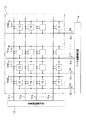
表示パネル部12は、図2に示すように、その行方向に沿って延びるn本の走査線Y1,Y2,・・・,Ynを備えている。また、表示パネル部12は、その列方向に沿って延びるm本のデータ線X1,X2,・・・,Xmを備えている。そして、表示パネル部12は、前記各走査線Y1,Y2,・・・,Ynと前記各データ線X1,X2,・・・,Xmとの交差部に対応した位置に画素回路15が配設されている。前記各画素回路15は、前記走査線Y1,Y2,・・・,Ynを介して走査線駆動回路13に接続されている。又、各画素回路15は、前記データ線X1,X2,・・・,Xmを介してデータ線駆動回路14に接続されている。ここで、前記m本のデータ線X1,X2,・・・,Xmは、i個の組に区分され、その区分された各組に予め定めた本数(j本)のデータ線が割り当てられた構成になっている。そして、説明の便宜上、m本のデータ線X1,X2,・・・,Xmを、他の組のデータ線と区別する場合には、データ線Xi.1,Xi.2,・・・,Xi.jと表記する。尚、データ線X1.1,X1.2,・・・,X1.j、X2.1,X2.2,・・・,X2.j、Xi.1,Xi.2,・・・,Xi.jは、この記載した順番で図2において左から右に形成されているものとする。更に、各画素回路15は、列方向に伸びるm本の電源線L1,L2,・・・,Lmと接続されている。電源線L1,L2,・・・,Lmはそれぞれ前記画素回路15を構成する後記する変換トランジスタTc及び駆動トランジスタTdに駆動電圧Vddを供給する。
【0060】
図3は、m番目のデータ線Xm(i.j)とn番目の走査線Ynとの交差部にそれぞれ対応して配設された画素回路15の回路図である。
画素回路15は、その発光層が有機材料で構成された有機EL素子16、駆動トランジスタTd、第1及び第2のスイッチングトランジスタTsw1,Tsw2、変換トランジスタTc及び保持キャパシタCoを備えている。駆動トランジスタTd、変換トランジスタTc及び第2のスイッチングトランジスタTsw2は、それぞれ、p型TFTである。また、第1のスイッチングトランジスタTsw1はn型TFTである。
【0061】
駆動トランジスタTdは、そのドレインが有機EL素子16の陽極に接続されている。有機EL素子16の陰極は接地されている。駆動トランジスタTdのゲートは変換トランジスタTcのゲートに接続されている。また、駆動トランジスタTdのソースは、変換トランジスタTcのソースに接続されている。さらに、駆動トランジスタTdのソースは、駆動電圧Vddを供給するm番目の電源線Lmに接続されている。また、駆動トランジスタTdのソース/ゲート間には、保持キャパシタCoが接続されている。つまり、前記変換トランジスタTcと駆動トランジスタTdとでカレントミラー回路を構成している。
【0062】
前記変換トランジスタTcのドレインは、第1のスイッチングトランジスタTsw1を介してm番目のデータ線Xm(Xi.j)に接続されている。また、変換トランジスタTcのドレインは、第2のスイッチングトランジスタTsw2を介して前記保持キャパシタCoに接続されている。
【0063】
前記第1のスイッチングトランジスタTsw1のゲートはn番目の第1の副走査線Yn1に接続されている。また、前記第2のスイッチングトランジスタTsw2のゲートはn番目の第2の副走査線Yn2に接続されている。前記第1の副走査線Yn1と第2の副走査線Yn2とでn番目の走査線Ynを構成している。
【0064】
尚、本実施形態においては、画素回路15を、有機EL素子16と、駆動トランジスタTdと、第1及び第2のスイッチングトランジスタTsw1,Tsw2と、変換トランジスタTcと、保持キャパシタCoとで構成したが、これに限定されるものではなく、適宜変更してもよい。
【0065】
走査線駆動回路13は、信号生成回路11から出力される前記走査制御信号に基づいて、表示パネル部12に設けられた前記n本の走査線Y1,Y2,・・・,Ynのうち、1本の走査線を選択し、その選択された走査線に走査信号を出力する。そして、その走査信号によって、前記画素回路15の有機EL素子16が発光するタイミング及び保持キャパシタCoへ後記するデータ電流IDに応じた電荷を書き込むタイミングを制御する。
【0066】
データ線駆動回路14は、信号生成回路11から出力された前記画像デジタルデータに基づいてデータ電流IDを生成するとともに、その生成されたデータ電流IDを対応する前記データ線X1,X2,・・・,Xmに供給する。そして、データ電流IDは、その対応する前記データ線X1,X2,・・・,Xmを介して各画素回路15に出力される。
【0067】
そして、走査線駆動回路13から出力される前記走査信号によって選択された走査線Y1,Y2,・・・,Yn上の各画素回路15においては、その第1及び第2のスイッチングトランジスタTsw1,Tsw2がそれぞれオン状態に設定される。このことによって、データ線駆動回路14から出力されたデータ電流IDに対応した電荷が前記第1及び第2のスイッチングトランジスタTsw1,Tsw2を介して保持キャパシタCoに書き込まれる。その後、走査線駆動回路13から出力される前記走査信号によって第2のスイッチングトランジスタTsw2がオフ状態に設定される。
【0068】
すると、前記変換トランジスタTcには保持キャパシタCoに書き込まれた電荷に応じた電流が流れる。そして、前記変換トランジスタTcとカレントミラー回路を構成する前記駆動トランジスタTdに前記電流に応じた大きさの駆動電流Ielが流れる。このことによって、有機EL素子16が前記駆動電流Ielに応じた輝度階調で発光する。通常、書き込み速度を速くするために、データ電流ID(変換トランジスタTcに流れる電流)は駆動電流(駆動トランジスタTdに流れる電流)より大きな電流とする。つまり、変換トランジスタTcと駆動トランジスタTdとはその利得係数を変えている。このため、駆動トランジスタTdに流れる電流はその利得係数の比に応じた電流である。
【0069】
次に、このように構成された有機ELディスプレイ10のデータ線駆動回路14について図4及び図5に従って詳述する。
図4は、データ線駆動回路14の内部構成図である。図4に示すように、データ線駆動回路14は、制御回路20と複数(本実施形態では、前記データ線X1,X2,・・・,Xmを区分した組数であるi個)の単一ラインドライバRD1〜RDiとを備えている。制御回路20は、i個の単一ラインドライバRD1〜RDiの各々と電気的に接続されている。
【0070】
制御回路20は、信号生成回路11から出力される前記6ビットの画像デジタルデータを各単一ラインドライバRD1〜RDiに供給する。
各単一ラインドライバRD1〜RDiは、それぞれ前記区分した各組毎に対応して設けられている。各単一ラインドライバRD1〜RDiは接続線Lpを介してカスケード接続されている。そして、第1の単一ラインドライバRD1はデータ線X1.1〜X1.jが、第2の単一ラインドライバRD2はデータ線X2.1〜X2.jが、・・・、第iの単一ラインドライバRDiはデータ線Xi.1〜Xi.jがそれぞれアナログ出力端子Uaを介して接続されている。本実施形態では、データ線X1.1〜X1.jと接続する第1の単一ラインドライバRD1をマスタードライバといい、第2〜第iの単一ラインドライバRD2〜RDiをスレーブドライバという。
【0071】
各単一ラインドライバRD1〜RDiは、それぞれ前記データ線の組に割り当てられたデータ線の本数に対応した数(j個)のデジタル・アナログ変換回路21aがそれぞれ備えている。そのj個のデジタル・アナログ変換21は、カスケード接続されている。そして、第1の単一ラインドライバRD1のデータ線X1.1に接続されたデジタル・アナログ変換回路21aの入力端子Piに基準電圧Vrefが供給されるようになっている。
【0072】
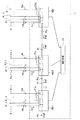
次に、前記したデジタル・アナログ変換回路21aを図5に従って説明する。尚、各単一ラインドライバRD1〜RDiに設けられた各デジタル・アナログ変換回路21aの回路構成は実質同じなので、説明の便宜上、m−1番目のデータ線Xm−1(Xi.j−1)と接続されるデジタル・アナログ変換回路21aについて説明する。
【0073】
デジタル・アナログ変換回路21aは、本実施形態においては6ビットの電流出力型デジタル・アナログ型変換回路である。デジタル・アナログ変換回路21aは、第1及び第2の変換用トランジスタQa,Qb、電流用トランジスタQcc、第1〜6の電流供給用トランジスタQd1〜Qd6、第1〜6のスイッチング用トランジスタQs1〜Qs6及び基準電流生成用トランジスタQrefを含んでいる。また、デジタル・アナログ変換回路21aは、6本のアナログ信号線22a〜22fと6本のデジタル信号線23a〜23fとを備えている。
【0074】
第1及び第2の変換用トランジスタQa,Qb、第1〜6の電流供給用トランジスタQd1〜Qd6、電流用トランジスタQcc及び基準電流生成用トランジスタQrefはそれぞれ所定の電流レベルを出力する定電流源として機能するトランジスタである。また、第1〜6のスイッチング用トランジスタQs1〜Qs6は、前記画像デジタルデータに応じてオン・オフ制御されるスイッチング素子として機能するトランジスタである。尚、本実施形態においては、前記第1の変換用トランジスタQa、第1〜6の電流供給用トランジスタQd1〜Qd6、第1〜6のスイッチング用トランジスタQs1〜Qs6及び基準電流生成用トランジスタQrefの導電型は、それぞれ、n型である。また、前記第2の変換用トランジスタQb及び電流用トランジスタQccの導電型は、それぞれ、p型である。
【0075】
アナログ信号線22a〜22fは互いに並列に配列され、その一端がそれぞれ前記アナログ出力端子Uaに接続されている。アナログ出力端子Uaは、データ線Xm−1(Xi.j−1)に接続されている。
【0076】
また、アナログ信号線22a〜22fは、それぞれ、対応する第1〜6のスイッチング用トランジスタQs1〜Qs6のドレインに接続されている。前記第1〜6のスイッチング用トランジスタQs1〜Qs6は、その各ゲートがそれぞれ対応する第1〜6のデジタル信号線23a〜23fを介して第1〜6のデジタル入力端子Ud1〜Ud6に接続されている。第1〜6のデジタル入力端子Ud1〜Ud6はそれぞれ前記制御回路20に接続されている。そして、前記第1〜6のスイッチング用トランジスタQs1〜Qs6は、後記するように、前記制御回路20から出力される前記画像デジタルデータに応じてオン・オフ制御される。
【0077】
また、前記第1〜6のスイッチング用トランジスタQs1〜Qs6の各ソースは、対応する第1〜6の電流供給用トランジスタQd1〜Qd6の各ドレインに接続されている。また、前記第1〜6の電流供給用トランジスタQd1〜Qd6のそれぞれのソースは共通して接地されている。即ち、前記第1〜6のスイッチング用トランジスタQs1〜Qs6と第1〜6の電流供給用トランジスタQd1〜Qd6とからなる電流経路は、アナログ出力端子Uaに接続されている。
【0078】
また、前記第1〜6の電流供給用トランジスタQd1〜Qd6は、その各利得係数βに応じたレベルの電流が流れる。ここで、第1〜6の電流供給用トランジスタQd1〜Qd6は、その各利得係数βの相対比が、それぞれ、1:2:4:8:16:32となるように設定されている。トランジスタの利得係数βは、β=(μCW/L)で定義される。ここで、μはキャリアの移動度、Cはゲート容量、Wはチャネル幅、Lはチャネル長である。従って、各第1〜6の電流供給用トランジスタQd1〜Qd6の電流駆動能力比は、1:2:4:8:16:32となり、第1〜6の電流供給用トランジスタQd1〜Qd6からそれぞれ出力される電流の大きさIa〜Ifは、以下の関係になる。
【0079】
Ia=Ib/2=Ic/4=Id/8=Ie/16=If/32
そして、前記第1〜6のスイッチング用トランジスタQs1〜Qs6は、前記制御回路20から出力される6ビットの前記画像デジタルデータの各ビットに対応している。例えば、画像デジタルデータの最下位ビットは、利得係数が最も小さな(即ちβの相対値が1の)第1のスイッチング用トランジスタQs1に供給され、最上位ビットは、利得係数が最も大きな(即ちβの相対値が32の)第6のスイッチング用トランジスタQs6に出力されるようになっている。
【0080】
また、前記第1〜6の電流供給用トランジスタQd1〜Qd6の各ゲートは互いに接続されるとともに、ダイオード接続された第1の変換用トランジスタQaのゲートに接続されている。
【0081】
従って、前記第1の変換用トランジスタQaは、第1〜6の電流供給用トランジスタQd1〜Qd6のそれぞれとカレントミラー回路を構成している。つまり、各第1〜6の電流供給用トランジスタQd1〜Qd6は、前記第1の変換用トランジスタQaのゲートの電圧レベルを基準値とした電流Ia〜Ifをそれぞれ出力する。尚、本実施形態においては、前記第1の変換用トランジスタQaの利得係数は、前記第1の電流供給用トランジスタQd1の利得係数と同じである。従って、前記第1の変換用トランジスタQaに流れる電流Itと同じ電流レベルを有する電流が第1の電流供給用トランジスタQd1に電流Iaとして流れる。
【0082】
前記第1の変換用トランジスタQaのソースは接地されている。また、前記第1の変換用トランジスタQaのドレインは、電流用トランジスタQccのドレインに接続されている。電流用トランジスタQccのソースには電源電圧Voが供給されるようになっている。即ち、前記第1の変換用トランジスタQaは、電流用トランジスタQccと直列に接続されている。
【0083】
また、電流用トランジスタQccのゲートは、ダイオード接続された第2の変換用トランジスタQbのゲートに接続されている。第2の変換用トランジスタQbのソースには前記電源電圧Voが供給されるようになっている。また、第2の変換用トランジスタQbのドレインは入力端子Piが接続されている。
【0084】
従って、前記電流用トランジスタQccと前記第2の変換用トランジスタQbとはカレントミラー回路を構成している。つまり、電流用トランジスタQccは、第2の変換用トランジスタQbのゲートの電圧レベルを基準値とした電流を出力する。
【0085】
そして、前記入力端子Piに基準電圧Vrefが供給されるとともに、前記第1〜6のデジタル入力端子Ud1〜Ud6に前記画像デジタルデータが入力される。すると、その入力された画像デジタルデータに応じて第1〜6のスイッチング用トランジスタQs1〜Qs6がオン・オフ制御される。つまり、前記第1〜6のスイッチング用トランジスタQs1〜Qs6は、第1〜6の電流供給用トランジスタQd1〜Qd6からそれぞれ出力される電流Ia〜Ifを制御する。
【0086】
そして、前記画像デジタルデータに応じて第1〜6の電流供給用トランジスタQd1〜Qd6からそれぞれ出力される電流Ia〜Ifが重畳されることで、同画像デジタルデータに応じた大きさを有するデータ電流IDがアナログ出力端子Uaから出力される。つまり、デジタル・アナログ変換回路21aは、6ビットの画像デジタルデータに応じて有機EL素子16を64階調で制御することができる。
【0087】
このように構成されたデジタル・アナログ変換回路21aには、前記第1の変換用トランジスタQaとカレントミラー回路を構成する基準電流生成用トランジスタQrefが形成されている。詳しくは、基準電流生成用トランジスタQrefは、そのソースが前記第1〜6の電流供給用トランジスタQd1〜Qd6の各ソースに接続されている。また、基準電流生成用トランジスタQrefのドレインは出力端子Poに接続されている。そして、基準電流生成用トランジスタQrefのドレインは前記出力端子Poを介して隣接する他のデジタル・アナログ変換回路21aの入力端子Piに接続されている。即ち、基準電流生成用トランジスタQrefは、前記電流Ia〜Ifが流れる前記第1〜6のスイッチング用トランジスタQs1〜Qs6と第1〜6の電流供給用トランジスタQd1〜Qd6とからなる電流経路には設けられていない。従って、前記基準電流生成用トランジスタQrefから出力される基準電流Irefは、前記画像データによりオン状態とされた前記第1〜6のスイッチング用トランジスタQs1〜Qs6と直列に接続された前記第1〜6の電流供給用トランジスタQd1〜Qd6からなる電流経路には供給されず、他のデジタル・アナログ変換回路21aに供給される。
【0088】
また、前記基準電流生成用トランジスタQrefは、その利得係数βrefが前記第1の変換用トランジスタQaの利得係数と等しくなるように設定されている。従って、基準電流生成用トランジスタQrefに流れる基準電流Irefの電流レベルは、第1の変換用トランジスタQa及び第1の電流供給用トランジスタQd1に流れる電流の電流レベルと同じである。
【0089】
このように、前記基準電流生成用トランジスタQrefは、前記第1の電流供給用トランジスタQd1に流れる電流と同じ電流レベルを有する基準電流Irefを前記出力端子Poから出力することができる。そして、この出力端子Poから出力される基準電流Irefは、前記アナログ出力端子Uaから出力されるデータ電流IDとは関係なく独立した電流である。そして、前記基準電流Irefは、前記接続線Lpを介してデータ線Xmに接続されたデジタル・アナログ変換回路21aの第2の変換用トランジスタQbに出力される。
【0090】
前記データ線Xmに接続されたデジタル・アナログ変換回路21aの第2の変換用トランジスタQbは、前記データ線Xm−1に接続されたデジタル・アナログ変換回路21aの出力端子Poから出力される基準電流Irefが供給される。すると、そのデジタル・アナログ変換回路21aの電流用トランジスタQccのゲートの電圧が前記第2の変換用トランジスタQbに流れる電流Itのレベルに応じて設定される。そして、この第1の変換用トランジスタQaに流れる電流Itに応じた電圧が各第1〜6の電流供給用トランジスタQd1〜Qd6のゲートとともに基準電流生成用トランジスタQrefに供給される。
【0091】
従って、データ線Xmに接続されたデジタル・アナログ変換回路21aに含まれる各第1〜6の電流供給用トランジスタQd1〜Qd6は、前記データ線Xm−1に接続されたデジタル・アナログ変換回路21aの基準電流生成用トランジスタQrefを流れる前記基準電流Irefを基準値とした電流Ia〜Ifを出力する。つまり、データ線Xmに接続されたデジタル・アナログ変換回路21aは、前記データ線Xm−1に接続されたデジタル・アナログ変換回路21aの基準電流生成用トランジスタQrefを流れる前記基準電流Irefを基準値としたデータ電流IDを前記画像デジタルデータに基づいて生成することができる。
【0092】
このように、1つのデジタル・アナログ変換回路21aが生成した基準電流Irefは、次段のデジタル・アナログ変換回路21aの基準電流Irefとして使用される。つまり、第1の単一ラインドライバRD1にある先頭のデジタル・アナログ変換回路21aが生成した基準電流Irefが順次間にある各デジタル・アナログ変換回路21aに利用され且つ値を維持しつつ、第iの単一ラインドライバRDiにある最終段のデジタル・アナログ変換回路21aにまで供給される。従って、異なった単一ラインドライバRD1〜RDi間において、各デジタル・アナログ変換回路21aの第1〜6の電流供給用トランジスタQd1〜Qd6の閾値電圧等の特性ばらつきによって、同一画像デジタルデータに対して異なった大きさのデータ電流IDが出力されない。
【0093】
つまり、異なった単一ラインドライバRD1〜RDiのデジタル・アナログ変換回路21a間においては、その第1〜6の電流供給用トランジスタQd1〜Qd6に特性ばらつきが生じてしまう。そのため、基準電圧Vrefを基準値として、異なった単一ラインドライバRD1〜RDiのデジタル・アナログ変換回路21a間の第1〜6の電流供給用トランジスタQd1〜Qd6の各ゲートに前記基準電圧Vrefを供給すると、各単一ラインドライバRD1〜RDi間で同じ画像デジタルデータに対して異なった大きさのデータ電流IDが出力されることとなる。これに対して、本発明の有機ELディスプレイ10は、各単一ラインドライバRD1〜RDiは基準電流Irefを基準値とするため、各第1〜6の電流供給用トランジスタQd1〜Qd6はその閾値電圧の影響を受けることはない。その結果、異なった単一ラインドライバRD1〜RDi間において、同一画像デジタルデータに対して異なった大きさのデータ電流IDが出力されることはない。従って、画像デジタルデータに応じてデータ電流IDを精度良く制御することができる。この結果、有機ELディスプレイ10の表示品位を向上させることができる。
【0094】
また、前記デジタル・アナログ変換回路21aは前記したように構成することによって、全てのデータ線X1〜Xmに対して同じ回路構成で使用することができる。即ち、マスタードライバの第1のデータ線X1と接続されたデジタル・アナログ変換回路21aにおいては、その入力端子には基準電圧Vrefを供給するようにする。一方、他のデジタル・アナログ変換回路21aの入力端子には基準電流Irefを供給するようにする。この結果、単一ラインドライバRD1〜RDiを全て同じ回路構成で製造することができるので、その製造コストを削減することができる。
【0095】
尚、有機ELディスプレイ10、デジタル・アナログ変換回路21a、及び、データ線駆動回路14は、特許請求の範囲に記載の電気光学装置、電子回路、及び、データ電流供給回路または電子装置に対応している。また、前記第1の変換用トランジスタQa及び第2の変換用トランジスタQbは、それぞれ、特許請求の範囲に記載の第1のトランジスタ及び第6のトランジスタに対応している。更に、第1〜6の電流供給用トランジスタQd1〜Qd6及び第1〜6のスイッチング用トランジスタQs1〜Qs6は、それぞれ、特許請求の範囲に記載の複数の第2のトランジスタ及び第3のトランジスタに対応している。基準電流生成用トランジスタQref及びデータ電流IDは、特許請求の範囲に記載の第4のトランジスタ及び駆動電流量にそれぞれ対応している。
【0096】
また、前記第1〜6のデジタル信号線23a〜23f及びアナログ出力端子Uaは、特許請求の範囲に記載の信号線及び出力端子にそれぞれ対応している。さらに、前記第2の変換用トランジスタQbのゲート、第2〜6の電流供給用トランジスタのゲート及び第1〜6のスイッチング用トランジスタQs1〜Qs6のゲートは、それぞれ、特許請求の範囲に記載の第1の制御用端子、第2の制御用端子及び第3の制御用端子に対応している。また、前記基準電流生成用トランジスタのゲート、第1の電流供給用トランジスタのゲート、第1の変換用トランジスタQaのゲートは、それぞれ、特許請求の範囲に記載の第4の制御用端子、第5の制御用端子及び第6の制御用端子に対応している。
【0097】
前記実施形態の有機ELディスプレイによれば、以下のような特徴を得ることができる。
(1) 前記実施形態では、単一ラインドライバRD1〜RDiのデジタル・アナログ変換回路21aに第1〜6の電流供給用トランジスタQd1〜Qd6の各々とカレントミラー回路を構成する第1の変換用トランジスタQaと、カレントミラー回路を構成する基準電流生成用トランジスタQrefを形成した。そして、その基準電流生成用トランジスタQrefの利得係数βrefを前記第1の変換用トランジスタQaの利得係数と等しくなるように設定した。また、前記基準電流生成用トランジスタQrefの出力端子Poを隣接して形成される他の単一ラインドライバRD1〜RDiのデジタル・アナログ変換回路21aの入力端子Piに接続した。
【0098】
このようにすることによって、前記他の単一ラインドライバのデジタル・アナログ変換回路21aでは前記基準電流Irefを基準値として画像デジタルデータに応じたデータ電流IDを出力することができる。このとき、データ電流IDは、前記第1〜6の電流供給用トランジスタQd1〜Qd6の閾値電圧の影響を受けることはない。その結果、異なった単一ラインドライバRD1〜RDi間において、同一画像デジタルデータに対して異なった大きさのデータ電流IDが出力されることはない。従って、画像デジタルデータに応じてデータ電流IDを精度良く制御することができる。その結果、有機ELディスプレイ10の表示品位を向上させることができる。
【0099】
(2) 前記実施形態では、基準電流Irefを生成するマスタードライバとその基準電流Irefに応じて駆動するスレーブドライバの回路構成は全て同じである。従って、前記マスタードライバと前記スレーブドライバとを区別して使用する必要はない。この結果、単一ラインドライバの製造コストを削減することができる。
【0100】
(第2実施形態)
次に、第1実施形態で説明した電気光学装置としての有機ELディスプレイ10の電子機器の適用について図6に従って説明する。有機ELディスプレイ10は、モバイル型のパーソナルコンピュータ、携帯電話、デジタルカメラ等種々の電子機器に適用できる。
【0101】
図6は、モバイル型パーソナルコンピュータの構成を示す斜視図を示す。図6において、パーソナルコンピュータ30は、キーボード31を備えた本体部32と、前記有機ELディスプレイ10を用いた表示ユニット33とを備えている。この場合においても、有機ELディスプレイ10を用いた表示ユニット33の表示品位を向上させることができる。
【0102】
尚、発明の実施形態は、上記実施形態に限定されるものではなく、以下のように実施してもよい。
○上記実施形態では、画像デジタルデータを6ビットとし、その6ビットの画像デジタルデータに応じて、デジタル・アナログ変換回路21aを6ビットの電流出力型デジタル・アナログ型変換回路に適応した。これを6ビット以外のデジタル・アナログ型変換回路に適用してもよい。このようにすることで、上記実施形態と同様の効果を得ることができる。
【0103】
○上記実施形態では、デジタル・アナログ変換回路21aを構成する第1及び第2の変換用トランジスタQa,Qb、第1〜6の電流供給用トランジスタQd1〜Qd6の導電型をn型としたが、p型にしてもよい。このようにすることで、上記実施形態と同様の効果を得ることができる。
【0104】
○上記実施形態では、1色からなる有機EL素子16の画素回路15を設けた有機ELディスプレイ10であったが、赤色、緑色及び青色の3色の有機EL素子16に対して各色用の画素回路15を設けたELディスプレイに応用しても良い。
【0105】
○上記実施形態では、画素回路15に具体化して好適な効果を得たが、有機EL素子21以外の例えばLEDやFED等の発光素子のような電流駆動素子を駆動する単位回路に具体化してもよい。RAM等(特にMRAM)の記憶装置に具体化してもよい。
【0106】
○上記第1実施形態では、電流駆動素子として有機EL素子16について具体化したが、無機EL素子に具体化してもよい。つまり、無機EL素子からなる無機ELディスプレイに応用しても良い。
【図面の簡単な説明】
【図1】第1実施形態の有機ELディスプレイの電気的構成を示すブロック回路図である。
【図2】表示パネル部の回路構成を示すブロック回路図である。
【図3】画素回路の回路図である。
【図4】データ線駆動回路の内部構成図である。
【図5】デジタル・アナログ変換回路の回路図である。
【図6】第2実施形態を説明するためのモバイル型パーソナルコンピュータの構成を示す斜視図である。
【符号の説明】
ID・・・駆動電流量としてのデータ電流、Qa…第1のトランジスタとしての第1の変換用トランジスタ、Qb…第6のトランジスタとしての第2の変換用トランジスタ、Qd1〜Qd6…第2のトランジスタとしての第1〜第6の電流生成用トランジスタ、Qs1〜Qs6…第3のトランジスタとしての第1〜6のスイッチング用トランジスタ、Qref…第4のトランジスとしての基準電流生成用トランジスタ、10…電気光学装置としての有機ELディスプレイ、14…電子装置またはデータ電流供給回路としてのデータ線駆動回路、15…画素回路、16…電気光学素子としての有機EL素子、20…制御回路、21a…電子回路としてのデジタル・アナログ変換回路、70…電子機器としてのモバイル型パーソナルコンピュータ。[0001]
TECHNICAL FIELD OF THE INVENTION
The present invention relates to an electronic circuit, an electronic device, an electro-optical device, and an electronic device.
[0002]
[Prior art]
As one of display devices using organic EL elements, there is an active matrix display device including a driving transistor for controlling the organic EL element for each pixel circuit.
[0003]
This type of display device includes a data line driving circuit that outputs a data current corresponding to image data, which is digital data, to the pixel circuit via a data line. The data line drive circuit has a single line driver having a plurality of digital-to-analog conversion circuits therein, and converts the image data into an analog signal by the digital-to-analog conversion circuit. (See, for example, Patent Document 1).
[0004]
[Patent Document 1]
JP 2000-122608 A
[0005]
[Problems to be solved by the invention]
In general, the number of pixel circuits is very large, so that a plurality of single line drivers may be electrically connected to each other to form one data line driving circuit. However, each single line driver outputs different data currents for the same image data due to variations in the characteristics of the transistors constituting the digital-to-analog conversion circuit. As a result, the organic EL element emits light with different brightness for the same image data by the connected single line driver. This makes it impossible to provide an electro-optical device with excellent display quality.
[0006]
SUMMARY An advantage of some aspects of the invention is to provide an electronic device, an electro-optical device, and an electronic device that can suppress variation in characteristics of a transistor.
[0007]
[Means for Solving the Problems]
The electronic circuit according to the present invention includes a diode-connected first transistor having a first control terminal, and a second control terminal, wherein the first control terminal has the second control terminal. A plurality of second transistors having terminals connected thereto, and a plurality of third control terminals each having a third control terminal connected to a signal line, the plurality of third transistors being connected in series to each of the plurality of second transistors; A transistor having a fourth control terminal, a fourth transistor having the first control terminal connected to the fourth control terminal, and A third transistor that is turned on by an on signal supplied via the signal line, and a third transistor that is connected in series with the third transistor that is turned on among the plurality of second transistors; Two transistors, Ranaru current path is connected to one output terminal, said fourth transistor is not connected to the one output terminal.
[0008]
According to this, a digital-to-analog conversion circuit configured to output an analog current of a magnitude corresponding to the digital data supplied to the third transistor via the signal line is configured, and the first analog current is not related to the analog current. An electronic circuit that outputs a current using a transistor as a reference value can be provided.
[0009]
In this electronic circuit, the gain coefficient of the fourth transistor may be the same as the gain coefficient of the first transistor.
According to this, the current level of the analog current output from the fourth transistor can be made equal to the current level of the current flowing through the first transistor.
[0010]
The electronic circuit includes a fifth control terminal, a fifth transistor connected in series with the first transistor, and a sixth control terminal, wherein the fifth control terminal includes the fifth control terminal. And a sixth transistor connected to the diode and connected to the sixth control terminal.
According to this, the voltage level of the voltage generated at the first control terminal can be controlled by the current level of the current flowing through the sixth transistor.
[0011]
An electronic circuit according to the present invention includes a diode-connected first transistor having a first control terminal, and a plurality of second transistors that output a current using a voltage level of the first control terminal as a reference value. And a third control terminal each of which controls a current output from each of the plurality of second transistors in accordance with an on / off signal input to the third control terminal. A third transistor including a third transistor, a fourth transistor having a fourth control terminal, and outputting a current with a voltage level of the first control terminal as a reference value; Current flowing from each of the plurality of second transistors does not flow.
[0012]
According to this, a digital-to-analog conversion circuit configured to output an analog current of a magnitude corresponding to the digital data supplied to the third transistor via the signal line is configured, and the first analog current is not related to the analog current. An electronic circuit that outputs a current using a transistor as a reference value can be provided.
[0013]
An electronic circuit according to the present invention includes a diode-connected first transistor having a first control terminal, and a plurality of second transistors that output a current using a voltage level of the first control terminal as a reference value. And a third control terminal each of which controls a current output from each of the plurality of second transistors in accordance with an on / off signal input to the third control terminal. A third transistor, and a fourth transistor that outputs a current with the voltage level of the first control terminal as a reference value, of the plurality of third transistors, A current path including a third transistor that is turned on and a second transistor connected in series with the third transistor that is turned on among the plurality of second transistors is provided in a current path. The fourth transistor is not provided.
[0014]
According to this, a digital-to-analog conversion circuit configured to output an analog current of a magnitude corresponding to the digital data supplied to the third transistor via the signal line is configured, and the first analog current is not related to the analog current. An electronic circuit that outputs a current using a transistor as a reference value can be provided.
[0015]
In this electronic circuit, the gain coefficient of the fourth transistor may be the same as the gain coefficient of the first transistor.
According to this, the current level of the analog current output from the fourth transistor can be made equal to the current level of the current flowing through the first transistor.
[0016]
The electronic circuit includes a fifth control terminal, a fifth transistor connected in series with the first transistor, and a sixth control terminal, wherein the fifth control terminal includes the fifth control terminal. And a sixth transistor connected to the diode and connected to the sixth control terminal.
According to this, the voltage level of the voltage generated at the first control terminal can be controlled by the current level of the current flowing through the sixth transistor.
[0017]
An electronic device according to the present invention is an electronic device including a plurality of unit circuits, wherein each of the plurality of unit circuits includes a first transistor connected to a diode, a first transistor having a first control terminal, and a second transistor. A plurality of second transistors each having a control terminal, the second control terminal being connected to the first control terminal, and a third control terminal each being connected to a signal line; A plurality of third transistors connected in series to each of the plurality of second transistors; and a fourth control terminal, wherein the fourth control terminal is connected to the first control terminal. A fourth transistor not provided in a current path including a second transistor connected in series to the third transistor turned on by an on signal supplied via the signal line; , Comprising the Is connected to another unit circuit via a connection line, and controls a voltage level of a first control terminal included in another unit circuit in accordance with a current level output from the fourth transistor. I do.
[0018]
According to this, a current generated in one unit circuit is used as a reference current, and the reference current is supplied to the first transistor of each of the other unit circuits. Then, the voltage of the first control terminal of the first transistor of each of the other unit circuits is controlled according to the reference current. Since the first transistor is driven using the reference current as a reference value, it is possible to suppress a variation in characteristics such as a threshold voltage of the first transistor between unit circuits. As a result, each unit circuit can accurately output a current corresponding to the on / off signal input to each of the third transistors.
[0019]
In this electronic device, the gain coefficient of the fourth transistor in each of the plurality of unit circuits may be the same as the gain coefficient of the first transistor.
According to this, the current level of the current flowing through the first transistor of one unit circuit can be made equal to the current level of the current flowing through all the first transistors of the other unit circuits.
[0020]
In this electronic device, each of the plurality of unit circuits includes a fifth control terminal, a fifth transistor connected in series with the first transistor, and a sixth control terminal, A sixth transistor diode-connected with the fifth control terminal connected to the sixth control terminal may be provided.
According to this, the voltage level of the voltage generated at the first control terminal can be controlled by the current level of the current flowing through the sixth transistor.
[0021]
The electronic device according to the present invention is an electronic device including a plurality of unit circuits, wherein each of the plurality of unit circuits is provided with a first control terminal, a diode-connected first transistor, and the first transistor. A plurality of second transistors that output a current with the voltage level of the control terminal as a reference value, each of which has a third control terminal, and an on / off signal input to the third control terminal A third transistor for controlling a current output from each of the plurality of second transistors in accordance with the following, and a fourth control terminal, wherein a voltage level of the first control terminal is set as a reference value. And a fourth transistor that outputs a current, wherein the current output from the fourth transistor is a second transistor connected in series with the third transistor that is turned on by the on / off signal. Transis Not supplied to the current path composed of, it is supplied to the other unit circuits.
[0022]
According to this, each unit circuit outputs an analog current having a current level corresponding to the ON / OFF signal input to each third transistor, and is independent from the fourth transistor independently of the analog current. The supplied current is supplied to other unit circuits. Each of the other unit circuits sets the voltage of the first control terminal of the first transistor included in each of the unit circuits, using the current output from the fourth transistor as a reference current. Thus, each of the unit circuits can suppress variation in the characteristics of the first transistor. Therefore, it is possible to accurately control the analog current output from each unit circuit.
[0023]
The electronic device according to the present invention is an electronic device including a plurality of unit circuits, wherein each of the plurality of unit circuits is provided with a first control terminal, a diode-connected first transistor, and the first transistor. A plurality of second transistors that output a current with the voltage level of the control terminal as a reference value, each of which has a third control terminal, and an on / off signal input to the third control terminal A third transistor for controlling a current output from each of the plurality of second transistors in accordance with the following, and a fourth control terminal, wherein a voltage level of the first control terminal is set as a reference value. And a fourth transistor that outputs a current. The current output from the fourth transistor is a reference current that sets the voltage level of the first control terminal of another unit circuit.
[0024]
According to this, each unit circuit outputs an analog current having a current level corresponding to the ON / OFF signal input to each third transistor, and is independent from the fourth transistor independently of the analog current. The supplied current is supplied to other unit circuits. Each of the other unit circuits sets the voltage of the first control terminal of the first transistor included in each of the unit circuits, using the current output from the fourth transistor as a reference current. Thus, each of the unit circuits can suppress variation in the characteristics of the first transistor. Therefore, it is possible to accurately control the analog current output from each unit circuit.
[0025]
In this electronic device, the gain coefficient of the fourth transistor in each of the plurality of unit circuits may be the same as the gain coefficient of the first transistor.
According to this, the current level of the current flowing through the first transistor of one unit circuit is used as all the reference currents of the other unit circuits.
[0026]
In this electronic device, the plurality of unit circuits may be cascaded.
According to this, the analog current generated by the cascade-connected unit circuits can be accurately controlled according to the on / off signal input to the third control terminal.
[0027]
In this electronic device, each of the plurality of unit circuits includes a fifth control terminal, a fifth transistor connected in series with the first transistor, and a sixth control terminal, A diode-connected sixth transistor having a fifth control terminal connected to the sixth control terminal may be provided.
[0028]
According to this, the voltage level of the voltage generated at the first control terminal can be controlled by the current level of the current flowing through the sixth transistor.
The electronic device according to the present invention is an electronic device including a plurality of unit circuits, wherein each of the plurality of unit circuits is provided with a first control terminal, a diode-connected first transistor, and the first transistor. A plurality of second transistors that output a current with the voltage level of the control terminal as a reference value, each of which has a third control terminal, and an on / off signal input to the third control terminal A third transistor for controlling a current output from each of the plurality of second transistors in accordance with the following, and a fourth control terminal, wherein a voltage level of the first control terminal is set as a reference value. A fourth transistor for outputting a current, a fifth control terminal, a fifth transistor connected in series with the first transistor, and a sixth control terminal; Terminal for the sixth control A sixth transistor connected to a child and diode-connected, wherein the fourth transistor is turned on by the on / off signal of a unit circuit including the fourth transistor. The third transistor is not connected to the second transistor connected in series, but is connected to the sixth transistor included in another unit circuit.
[0029]
According to this, each unit circuit outputs an analog current having a current level corresponding to the ON / OFF signal input to each third transistor, and is independent from the fourth transistor independently of the analog current. The supplied current is supplied to other unit circuits. Each of the other unit circuits is supplied to the sixth transistor included in each of the unit circuits, using the current output from the fourth transistor as a reference current. Then, the voltage of the first control terminal of the first transistor is set by the reference current flowing through the sixth transistor. Thus, each of the unit circuits can suppress variation in the characteristics of the first transistor. Therefore, it is possible to accurately control the analog current output from each unit circuit.
[0030]
In this electronic device, the gain coefficient of the fourth transistor in each of the plurality of unit circuits may be the same as the gain coefficient of the first transistor.
According to this, the current level of the current flowing through the first transistor of one unit circuit can be made equal to the current level of the current flowing through all the first transistors of the other unit circuits.
[0031]
In this electronic device, the plurality of unit circuits may be cascaded.
According to this, the analog current generated by the cascade-connected unit circuits can be accurately controlled according to the on / off signal input to the third control terminal.
[0032]
An electro-optical device according to an aspect of the invention includes a plurality of scanning lines, a plurality of data lines, and an electro-optical element disposed corresponding to an intersection of each of the scanning lines and each of the data lines. A data current supply circuit for supplying a data current to each of the data lines, wherein the data current supply circuit supplies a drive current amount corresponding to the data current to each of the electro-optical elements. A plurality of second transistors including a diode-connected first transistor having a first control terminal and a second control terminal having the second control terminal connected to the first control terminal. And a third control terminal connected to a signal line for supplying image data, a plurality of third transistors connected in series with each of the plurality of second transistors, and Control of 4 And a fourth transistor having the fourth control terminal connected to the first control terminal, wherein the fourth transistor is connected to another data current supply circuit via a connection line. And a voltage level of a first control terminal included in another data current supply circuit is controlled in accordance with a current level output from the fourth transistor.
[0033]
According to this, it is possible to configure a digital-to-analog conversion circuit that outputs an analog current having a magnitude corresponding to image data, and to output a current using a first transistor that is not related to the analog current as a reference value. Can be. Thus, the variation in the characteristics of the first transistor of each unit circuit can be suppressed, so that an analog current having a magnitude corresponding to the image data can be output with high accuracy. As a result, an electro-optical device having excellent display quality can be provided.
[0034]
In this electro-optical device, the gain coefficient of the fourth transistor may be the same as the gain coefficient of the first transistor.
According to this, the current level of the current flowing through the first transistor of one unit circuit can be made equal to the current level of the current flowing through all the first transistors of the other unit circuits.
[0035]
In this electro-optical device, the data current supply circuit includes a fifth control terminal, a fifth transistor connected in series with the first transistor, and a sixth control terminal. A fifth transistor connected to the fifth control terminal may be connected to the sixth control terminal.
[0036]
According to this, the voltage level of the voltage generated at the first control terminal can be controlled by the current level of the current flowing through the sixth transistor.
An electro-optical device according to an aspect of the invention includes a plurality of scanning lines, a plurality of data lines, and an electro-optical element disposed corresponding to an intersection of each of the scanning lines and each of the data lines. A data current supply circuit that supplies a data current to each of the data lines; and an electro-optical device that supplies a drive current amount according to the data current to each of the electro-optical elements. A diode-connected first transistor having one control terminal, a plurality of second transistors that output a current based on a voltage level of the first control terminal as a reference value, and A third transistor for controlling a current output from each of the plurality of second transistors in accordance with image data input to the third control terminal, and a fourth control And a fourth transistor that outputs a current with the voltage level of the first control terminal as a reference value, wherein the current output from the fourth transistor is turned on by the image data. The current is not supplied to the current path composed of the second transistor connected in series with the third transistor and is supplied to another unit circuit.
[0037]
According to this, each unit circuit outputs an analog current having a current level corresponding to the ON / OFF signal input to each third transistor, and is independent from the fourth transistor independently of the analog current. The supplied current is supplied to other unit circuits. Each of the other unit circuits sets the voltage of the first control terminal of the first transistor included in each of the unit circuits, using the current output from the fourth transistor as a reference current. Thus, each of the unit circuits can suppress variation in the characteristics of the first transistor. Therefore, it is possible to accurately control the analog current output from each unit circuit. As a result, an electro-optical device having excellent display quality can be provided.
[0038]
An electro-optical device according to an aspect of the invention includes a plurality of scanning lines, a plurality of data lines, and an electro-optical element disposed corresponding to an intersection of each of the scanning lines and each of the data lines. A data current supply circuit that supplies a data current to each of the data lines; and an electro-optical device that supplies a drive current amount according to the data current to each of the electro-optical elements. A diode-connected first transistor having one control terminal, a plurality of second transistors that output a current based on a voltage level of the first control terminal as a reference value, and A third transistor for controlling a current output from each of the plurality of second transistors in accordance with image data input to the third control terminal, and a fourth control A fourth transistor that has a terminal and outputs a current with a voltage level of the first control terminal as a reference value, and the current output from the fourth transistor is the fourth transistor of another unit circuit. 1 is a reference current for setting the voltage level of the control terminal.
[0039]
According to this, each unit circuit outputs an analog current having a current level corresponding to the ON / OFF signal input to each third transistor, and is independent from the fourth transistor independently of the analog current. The supplied current is supplied to other unit circuits. Each of the other unit circuits sets the voltage of the first control terminal of the first transistor included in each of the unit circuits, using the current output from the fourth transistor as a reference current. Thus, each of the unit circuits can suppress variation in the characteristics of the first transistor. Therefore, it is possible to accurately control the analog current output from each unit circuit. As a result, an electro-optical device having excellent display quality can be provided.
[0040]
In the electro-optical device, a gain coefficient of the fourth transistor in each of the plurality of data current supply circuits may be the same as a gain coefficient of the first transistor.
According to this, the current level of the current flowing through the first transistor of one unit circuit can be made equal to the current level of the current flowing through all the first transistors of the other unit circuits.
[0041]
In this electro-optical device, the plurality of data current supply circuits may be cascaded.
According to this, the analog current generated by the data current supply circuit connected in cascade can be controlled accurately in accordance with the on / off signal input to the third control terminal.
[0042]
In this electro-optical device, each of the data current supply circuits includes a fifth control terminal, a fifth transistor connected in series with the first transistor, and a sixth control terminal. A diode-connected sixth transistor having a fifth control terminal connected to the sixth control terminal may be provided.
According to this, the voltage level of the voltage generated at the first control terminal can be controlled by the current level of the current flowing through the sixth transistor.
[0043]
An electro-optical device according to an aspect of the invention includes a plurality of scanning lines, a plurality of data lines, and an electro-optical element disposed corresponding to an intersection of each of the scanning lines and each of the data lines. A data current supply circuit for supplying a data current to each of the data lines, wherein the data current supply circuit supplies a drive current amount corresponding to the data current to each of the electro-optical elements. A first transistor which is diode-connected, and a plurality of second transistors which output a current with the voltage level of the first control terminal as a reference value; A third transistor having a control terminal, and controlling a current output from each of the plurality of second transistors in response to an on / off signal input to the third control terminal; System A fourth transistor that outputs a current with the voltage level of the first control terminal as a reference value, and a fifth control terminal, and is connected in series with the first transistor. A fifth transistor, comprising a sixth control terminal, wherein the fifth control terminal is connected to the sixth control terminal, and a diode-connected sixth transistor; The fourth transistor is not connected to the second transistor connected in series with the third transistor turned on by the on / off signal of the unit circuit including the fourth transistor, and other transistors are not connected. It is connected to the sixth transistor included in the unit circuit.
[0044]
According to this, each unit circuit outputs an analog current having a current level corresponding to the ON / OFF signal input to each third transistor, and is independent from the fourth transistor independently of the analog current. The supplied current is supplied to other unit circuits. Each of the other unit circuits is supplied to the sixth transistor included in each of the unit circuits, using the current output from the fourth transistor as a reference current. Then, the voltage of the first control terminal of the first transistor is set by the reference current flowing through the sixth transistor. Thus, each of the unit circuits can suppress variation in the characteristics of the first transistor. Therefore, it is possible to accurately control the analog current output from each unit circuit. As a result, an electro-optical device having excellent display quality can be provided.
[0045]
In the electro-optical device, a gain coefficient of the fourth transistor in each of the plurality of data current supply circuits may be the same as a gain coefficient of the first transistor.
[0046]
According to this, the current level of the current flowing through the first transistor of one unit circuit can be made equal to the current level of the current flowing through all the first transistors of the other unit circuits.
[0047]
In this electro-optical device, the plurality of data current supply circuits may be cascaded.
According to this, the analog current generated by the cascade-connected unit circuits can be accurately controlled according to the on / off signal input to the third control terminal.
[0048]
In this electro-optical device, the data current supply circuit includes a fifth control terminal, a fifth transistor connected in series with the first transistor, and a sixth control terminal. A fifth transistor connected to the fifth control terminal may be connected to the sixth control terminal.
[0049]
According to this, the voltage level of the voltage generated at the first control terminal can be controlled by the current level of the current flowing through the sixth transistor.
[0050]
In this electro-optical device, the gain coefficient of the sixth transistor may be the same as the gain coefficient of the first transistor.
According to this, the voltage level of the voltage generated at the first control terminal can be controlled by the current level of the current flowing through the sixth transistor.
[0051]
In this electro-optical device, the electro-optical element may be an EL element. According to this, the display quality of the electro-optical device including the EL element can be improved.
[0052]
In this electro-optical device, the EL element may have a light-emitting layer made of an organic material.
According to this, the display quality of the electro-optical device including the organic EL element can be improved.
[0053]
An electronic apparatus according to the present invention includes the above electronic device.
According to this, it is possible to provide an electronic device that controls accurately according to digital data.
[0054]
Electronic equipment according to the present invention includes the above-described electro-optical device.
According to this, an electro-optical device having excellent display quality can be provided.
[0055]
BEST MODE FOR CARRYING OUT THE INVENTION
(1st Embodiment)
Hereinafter, a first embodiment of the present invention will be described with reference to FIGS. FIG. 1 is a block circuit diagram showing an electrical configuration of the organic EL display. FIG. 2 is a block circuit diagram showing a circuit configuration of the display panel unit. FIG. 3 is a circuit diagram of the pixel circuit.
[0056]
The
[0057]
The
[0058]
The
[0059]
As shown in FIG. 2, the
[0060]
FIG. 3 is a circuit diagram of the
The
[0061]
The drain of the driving transistor Td is connected to the anode of the
[0062]
The drain of the conversion transistor Tc is connected to the m-th data line Xm (Xij) via the first switching transistor Tsw1. The drain of the conversion transistor Tc is connected to the holding capacitor Co via a second switching transistor Tsw2.
[0063]
The gate of the first switching transistor Tsw1 is connected to the n-th first sub-scanning line Yn1. The gate of the second switching transistor Tsw2 is connected to the n-th second sub-scanning line Yn2. The first sub-scanning line Yn1 and the second sub-scanning line Yn2 constitute an n-th scanning line Yn.
[0064]
In the present embodiment, the
[0065]
The scanning
[0066]
The data
[0067]
Then, in each
[0068]
Then, a current corresponding to the electric charge written to the holding capacitor Co flows through the conversion transistor Tc. Then, a drive current Iel having a magnitude corresponding to the current flows through the drive transistor Td forming a current mirror circuit together with the conversion transistor Tc. As a result, the
[0069]
Next, the data
FIG. 4 is an internal configuration diagram of the data line driving
[0070]
The
Each of the single line drivers RD1 to RDi is provided corresponding to each of the divided groups. Each of the single line drivers RD1 to RDi is cascaded via a connection line Lp. Then, the first single line driver RD1 is connected to the data lines X1.1 to X1. j is the second single line driver RD2 and the data lines X2.1 to X2. j,..., i-th single line driver RDi is connected to data line Xi. 1 to Xi. j are respectively connected via analog output terminals Ua. In the present embodiment, the data lines X1.1 to X1. The first single line driver RD1 connected to j is called a master driver, and the second to i-th single line drivers RD2 to RDi are called slave drivers.
[0071]
Each of the single line drivers RD1 to RDi is provided with a number (j) of digital /
[0072]
Next, the digital /
[0073]
The digital /
[0074]
The first and second conversion transistors Qa and Qb, the first to sixth current supply transistors Qd1 to Qd6, the current transistor Qcc, and the reference current generation transistor Qref are each a constant current source that outputs a predetermined current level. It is a functioning transistor. The first to sixth switching transistors Qs1 to Qs6 are transistors that function as switching elements that are turned on and off in accordance with the image digital data. In this embodiment, the conductivity of the first conversion transistor Qa, the first to sixth current supply transistors Qd1 to Qd6, the first to sixth switching transistors Qs1 to Qs6, and the reference current generation transistor Qref The types are each n-type. The conductivity types of the second conversion transistor Qb and the current transistor Qcc are each p-type.
[0075]
The
[0076]
The
[0077]
The sources of the first to sixth switching transistors Qs1 to Qs6 are connected to the drains of the corresponding first to sixth current supply transistors Qd1 to Qd6. The sources of the first to sixth current supply transistors Qd1 to Qd6 are commonly grounded. That is, the current path including the first to sixth switching transistors Qs1 to Qs6 and the first to sixth current supply transistors Qd1 to Qd6 is connected to the analog output terminal Ua.
[0078]
The first to sixth current supply transistors Qd1 to Qd6 flow a current of a level corresponding to each gain coefficient β. Here, the first to sixth current supply transistors Qd1 to Qd6 are set such that the relative ratios of the respective gain coefficients β are 1: 2: 4: 8: 16: 32. The gain coefficient β of the transistor is defined by β = (μCW / L). Here, μ is the carrier mobility, C is the gate capacitance, W is the channel width, and L is the channel length. Accordingly, the current driving capability ratio of each of the first to sixth current supply transistors Qd1 to Qd6 is 1: 2: 4: 8: 16: 32, and the output from the first to sixth current supply transistors Qd1 to Qd6 respectively. The magnitudes of the currents Ia to If are as follows.
[0079]
Ia = Ib / 2 = Ic / 4 = Id / 8 = Ie / 16 = If / 32
The first to sixth switching transistors Qs1 to Qs6 correspond to 6-bit image digital data output from the
[0080]
The gates of the first to sixth current supply transistors Qd1 to Qd6 are connected to each other and to the gate of the diode-connected first conversion transistor Qa.
[0081]
Therefore, the first conversion transistor Qa forms a current mirror circuit with each of the first to sixth current supply transistors Qd1 to Qd6. That is, the first to sixth current supply transistors Qd1 to Qd6 output currents Ia to If, respectively, using the voltage level of the gate of the first conversion transistor Qa as a reference value. In the present embodiment, the gain coefficient of the first conversion transistor Qa is the same as the gain coefficient of the first current supply transistor Qd1. Accordingly, a current having the same current level as the current It flowing through the first conversion transistor Qa flows as the current Ia through the first current supply transistor Qd1.
[0082]
The source of the first conversion transistor Qa is grounded. The drain of the first conversion transistor Qa is connected to the drain of the current transistor Qcc. The power supply voltage Vo is supplied to the source of the current transistor Qcc. That is, the first conversion transistor Qa is connected in series with the current transistor Qcc.
[0083]
The gate of the current transistor Qcc is connected to the gate of the diode-connected second conversion transistor Qb. The power supply voltage Vo is supplied to the source of the second conversion transistor Qb. The input terminal Pi is connected to the drain of the second conversion transistor Qb.
[0084]
Therefore, the current transistor Qcc and the second conversion transistor Qb constitute a current mirror circuit. That is, the current transistor Qcc outputs a current using the voltage level of the gate of the second conversion transistor Qb as a reference value.
[0085]
Then, the reference voltage Vref is supplied to the input terminal Pi, and the image digital data is input to the first to sixth digital input terminals Ud1 to Ud6. Then, on / off control of the first to sixth switching transistors Qs1 to Qs6 is performed according to the input image digital data. That is, the first to sixth switching transistors Qs1 to Qs6 control the currents Ia to If output from the first to sixth current supply transistors Qd1 to Qd6, respectively.
[0086]
The currents Ia to If output from the first to sixth current supply transistors Qd1 to Qd6 are superimposed in accordance with the image digital data, so that a data current having a magnitude corresponding to the image digital data is superimposed. The ID is output from the analog output terminal Ua. That is, the digital /
[0087]
In the digital /
[0088]
The reference current generating transistor Qref is set such that its gain coefficient βref is equal to the gain coefficient of the first conversion transistor Qa. Therefore, the current level of the reference current Iref flowing through the reference current generation transistor Qref is the same as the current level of the current flowing through the first conversion transistor Qa and the first current supply transistor Qd1.
[0089]
As described above, the reference current generation transistor Qref can output the reference current Iref having the same current level as the current flowing through the first current supply transistor Qd1 from the output terminal Po. The reference current Iref output from the output terminal Po is a current independent of the data current ID output from the analog output terminal Ua. Then, the reference current Iref is output to the second conversion transistor Qb of the digital /
[0090]
The second conversion transistor Qb of the digital /
[0091]
Therefore, each of the first to sixth current supply transistors Qd1 to Qd6 included in the digital /
[0092]
In this way, the reference current Iref generated by one digital /
[0093]
That is, among the digital /
[0094]
Further, by configuring the digital /
[0095]
The
[0096]
The first to sixth
[0097]
According to the organic EL display of the embodiment, the following features can be obtained.
(1) In the above embodiment, each of the first to sixth current supply transistors Qd1 to Qd6 and the first conversion transistor forming a current mirror circuit are provided in the digital /
[0098]
In this manner, the digital-to-
[0099]
(2) In the above embodiment, the circuit configurations of the master driver that generates the reference current Iref and the slave driver that drives in accordance with the reference current Iref are all the same. Therefore, it is not necessary to use the master driver and the slave driver separately. As a result, the manufacturing cost of a single line driver can be reduced.
[0100]
(2nd Embodiment)
Next, application of the electronic apparatus of the
[0101]
FIG. 6 is a perspective view showing a configuration of a mobile personal computer. In FIG. 6, the
[0102]
The embodiments of the present invention are not limited to the above embodiments, but may be implemented as follows.
In the above embodiment, the image digital data is 6 bits, and the digital /
[0103]
In the above embodiment, the conductivity types of the first and second conversion transistors Qa and Qb and the first to sixth current supply transistors Qd1 to Qd6 constituting the digital /
[0104]
In the above embodiment, the
[0105]
In the above embodiment, the
[0106]
In the first embodiment, the
[Brief description of the drawings]
FIG. 1 is a block circuit diagram illustrating an electrical configuration of an organic EL display according to a first embodiment.
FIG. 2 is a block circuit diagram illustrating a circuit configuration of a display panel unit.
FIG. 3 is a circuit diagram of a pixel circuit.
FIG. 4 is an internal configuration diagram of a data line driving circuit.
FIG. 5 is a circuit diagram of a digital / analog conversion circuit.
FIG. 6 is a perspective view showing a configuration of a mobile personal computer for describing a second embodiment.
[Explanation of symbols]
ID: data current as drive current amount; Qa: first conversion transistor as first transistor; Qb: second conversion transistor as sixth transistor; Qd1 to Qd6: second transistor First to sixth current generating transistors, Qs1 to Qs6... First to sixth switching transistors as third transistors, Qref... Reference current generating transistors as fourth transistors, 10. An organic EL display as a device, 14 a data line drive circuit as an electronic device or a data current supply circuit, 15 a pixel circuit, 16 an organic EL element as an electro-optical element, 20 a control circuit, 21a as an electronic circuit Digital-to-analog conversion circuit, 70: mobile personal computer as electronic equipment
Claims (35)
第2の制御用端子を備え、前記第1の制御用端子に前記第2の制御用端子が接続された複数の第2のトランジスタと、
各々が信号線に接続された第3の制御用端子を備え、前記複数の第2のトランジスタの各々に直列に接続された複数の第3のトランジスタと、
第4の制御用端子を備え、前記第1の制御用端子に前記第4の制御用端子が接続された第4のトランジスタと、を含み、
前記複数の第3のトランジスタのうち、前記信号線を介して供給されるオン信号によりオン状態とされた第3のトランジスタと、前記複数の第2のトランジスタのうち、前記オン状態とされた第3のトランジスタと直列に接続された第2のトランジスタと、からなる電流経路は一つの出力端子に接続され、
前記第4のトランジスタは前記一つの出力端子には接続されないことを特徴とする電子回路。A diode-connected first transistor having a first control terminal;
A plurality of second transistors comprising a second control terminal, wherein the second control terminal is connected to the first control terminal;
A plurality of third transistors each including a third control terminal connected to a signal line, and connected in series to each of the plurality of second transistors;
A fourth transistor, comprising: a fourth control terminal, wherein the fourth control terminal is connected to the first control terminal;
Of the plurality of third transistors, the third transistor turned on by an on signal supplied via the signal line, and the third transistor turned on among the plurality of second transistors. And a second transistor connected in series with the third transistor is connected to one output terminal,
The electronic circuit according to claim 1, wherein the fourth transistor is not connected to the one output terminal.
前記第4のトランジスタの利得係数は、前記第1のトランジスタの利得係数と同じであることを特徴とする電子回路。The electronic circuit according to claim 1,
The electronic circuit according to claim 1, wherein a gain coefficient of the fourth transistor is the same as a gain coefficient of the first transistor.
第5の制御用端子を備え、前記第1のトランジスタと直列に接続された第5のトランジスタと、
第6の制御用端子を備え、前記第5の制御用端子が前記第6の制御用端子に接続された、ダイオード接続された第6のトランジスタと
を備えたことを特徴とする電子回路。The electronic circuit according to claim 1 or 2,
A fifth transistor including a fifth control terminal and connected in series with the first transistor;
An electronic circuit comprising: a sixth control terminal; and a sixth diode-connected transistor, wherein the fifth control terminal is connected to the sixth control terminal.
前記第1の制御用端子の電圧レベルを基準値とした電流を出力する複数の第2のトランジスタと、
各々が第3の制御用端子を備え、前記第3の制御用端子に入力されるオン・オフ信号に応じて前記複数の第2のトランジスタの各々から出力される電流を制御する第3のトランジスタと、
第4の制御用端子を備え、前記第1の制御用端子の電圧レベルを基準値とした電流を出力する第4のトランジスタと、を含み、
前記第4のトランジスタから出力される電流は、前記複数の第2のトランジスタの各々から出力される電流経路には流れないようにしたことを特徴とする電子回路。A diode-connected first transistor having a first control terminal;
A plurality of second transistors that output a current with the voltage level of the first control terminal as a reference value;
Third transistors each having a third control terminal and controlling a current output from each of the plurality of second transistors in accordance with an on / off signal input to the third control terminal When,
A fourth transistor that has a fourth control terminal and outputs a current with a voltage level of the first control terminal as a reference value;
An electronic circuit, wherein a current output from the fourth transistor does not flow in a current path output from each of the plurality of second transistors.
前記第1の制御用端子の電圧レベルを基準値とした電流を出力する複数の第2のトランジスタと、
各々が第3の制御用端子を備え、前記第3の制御用端子に入力されるオン・オフ信号に応じて前記複数の第2のトランジスタの各々から出力される電流を制御する第3のトランジスタと、
前記第1の制御用端子の電圧レベルを基準値とした電流を出力する第4のトランジスタと、を含み、
前記複数の第3のトランジスタのうち、前記オン・オフ信号によりオン状態とされた第3のトランジスタと、前記複数の第2のトランジスタのうち、前記オン状態とされた第3のトランジスタと直列に接続された第2のトランジスタと、からなる電流経路には、前記第4のトランジスタは設けられていないことを特徴とする電子回路。A diode-connected first transistor having a first control terminal;
A plurality of second transistors that output a current with the voltage level of the first control terminal as a reference value;
Third transistors each having a third control terminal and controlling a current output from each of the plurality of second transistors in accordance with an on / off signal input to the third control terminal When,
A fourth transistor that outputs a current with a voltage level of the first control terminal as a reference value,
Of the plurality of third transistors, the third transistor turned on by the on / off signal and the third transistor turned on among the plurality of second transistors are connected in series. An electronic circuit, wherein the fourth transistor is not provided in a current path including a connected second transistor.
前記第4のトランジスタの利得係数は、前記第1のトランジスタの利得係数と同じであることを特徴とする電子回路。The electronic circuit according to claim 4, wherein
The electronic circuit according to claim 1, wherein a gain coefficient of the fourth transistor is the same as a gain coefficient of the first transistor.
第5の制御用端子を備え、前記第1のトランジスタと直列に接続された第5のトランジスタと、
第6の制御用端子を備え、前記第5の制御用端子が前記第6の制御用端子に接続された、ダイオード接続された第6のトランジスタと
を備えたことを特徴とする電子回路。The electronic circuit according to any one of claims 4 to 6,
A fifth transistor including a fifth control terminal and connected in series with the first transistor;
An electronic circuit comprising: a sixth control terminal; and a sixth diode-connected transistor, wherein the fifth control terminal is connected to the sixth control terminal.
前記複数の単位回路の各々は、
第1の制御用端子を備えた、ダイオード接続された第1のトランジスタと、
第2の制御用端子を備え、前記第1の制御用端子に前記第2の制御用端子が接続された複数の第2のトランジスタと、
各々が信号線に接続された第3の制御用端子を備え、前記複数の第2のトランジスタの各々に直列に接続された複数の第3のトランジスタと、
第4の制御用端子を備え、前記第1の制御用端子に前記第4の制御用端子が接続されるとともに、前記信号線を介して供給されるオン信号によりオン状態とされた前記第3のトランジスタと直列に接続された第2のトランジスタからなる電流経路には設けられていない第4のトランジスタと、を含み、
前記第4のトランジスタは、接続線を介して他の単位回路に接続され、前記第4のトランジスタから出力される電流レベルに応じて、他の単位回路に含まれる第1の制御用端子の電圧レベルを制御することを特徴とする電子装置。In an electronic device including a plurality of unit circuits,
Each of the plurality of unit circuits,
A diode-connected first transistor having a first control terminal;
A plurality of second transistors comprising a second control terminal, wherein the second control terminal is connected to the first control terminal;
A plurality of third transistors each including a third control terminal connected to a signal line, and connected in series to each of the plurality of second transistors;
A fourth control terminal, wherein the fourth control terminal is connected to the first control terminal, and the third control terminal is turned on by an on signal supplied through the signal line; A fourth transistor not provided in a current path composed of a second transistor connected in series with the transistor of
The fourth transistor is connected to another unit circuit via a connection line, and a voltage of a first control terminal included in the other unit circuit according to a current level output from the fourth transistor. An electronic device characterized by controlling a level.
前記複数の単位回路の各々の前記第4のトランジスタの利得係数は、前記第1のトランジスタの利得係数と同じであることを特徴とする電子装置。The electronic device according to claim 8,
The electronic device according to claim 1, wherein a gain coefficient of the fourth transistor in each of the plurality of unit circuits is the same as a gain coefficient of the first transistor.
前記複数の単位回路の各々は、
第5の制御用端子を備え、前記第1のトランジスタと直列に接続された第5のトランジスタと、
第6の制御用端子を備え、前記第5の制御用端子が前記第6の制御用端子に接続された、ダイオード接続された第6のトランジスタと
を備えたことを特徴とする電子装置。The electronic device according to claim 8, wherein
Each of the plurality of unit circuits,
A fifth transistor including a fifth control terminal and connected in series with the first transistor;
An electronic device comprising: a sixth control terminal; and a sixth diode-connected transistor, wherein the fifth control terminal is connected to the sixth control terminal.
前記複数の単位回路の各々は、
第1の制御用端子を備えた、ダイオード接続された第1のトランジスタと、
前記第1の制御用端子の電圧レベルを基準値とした電流を出力する複数の第2のトランジスタと、
各々が第3の制御用端子を備え、前記第3の制御用端子に入力されるオン・オフ信号に応じて前記複数の第2のトランジスタの各々から出力される電流を制御する第3のトランジスタと、
第4の制御用端子を備え、前記第1の制御用端子の電圧レベルを基準値とした電流を出力する第4のトランジスタと、を含み、
前記第4のトランジスタから出力される電流は、前記オン・オフ信号によりオン状態とされた前記第3のトランジスタと直列に接続された第2のトランジスタからなる電流経路には供給されず、他の単位回路に供給されることを特徴とする電子装置。In an electronic device including a plurality of unit circuits,
Each of the plurality of unit circuits,
A diode-connected first transistor having a first control terminal;
A plurality of second transistors that output a current with the voltage level of the first control terminal as a reference value;
Third transistors each having a third control terminal and controlling a current output from each of the plurality of second transistors in accordance with an on / off signal input to the third control terminal When,
A fourth transistor that has a fourth control terminal and outputs a current with a voltage level of the first control terminal as a reference value;
The current output from the fourth transistor is not supplied to a current path including a second transistor connected in series with the third transistor turned on by the on / off signal, and is not supplied to another current path. An electronic device supplied to a unit circuit.
前記複数の単位回路の各々は、
第1の制御用端子を備えた、ダイオード接続された第1のトランジスタと、
前記第1の制御用端子の電圧レベルを基準値とした電流を出力する複数の第2のトランジスタと、
各々が第3の制御用端子を備え、前記第3の制御用端子に入力されるオン・オフ信号に応じて前記複数の第2のトランジスタの各々から出力される電流を制御する第3のトランジスタと、
第4の制御用端子を備え、前記第1の制御用端子の電圧レベルを基準値とした電流を出力する第4のトランジスタと、を含み、
前記第4のトランジスタから出力される電流は、他の単位回路の第1の制御用端子の電圧レベルを設定する基準電流となることを特徴とする電子装置。In an electronic device including a plurality of unit circuits,
Each of the plurality of unit circuits,
A diode-connected first transistor having a first control terminal;
A plurality of second transistors that output a current with the voltage level of the first control terminal as a reference value;
Third transistors each having a third control terminal and controlling a current output from each of the plurality of second transistors in accordance with an on / off signal input to the third control terminal When,
A fourth transistor that has a fourth control terminal and outputs a current with a voltage level of the first control terminal as a reference value;
An electronic device, wherein a current output from the fourth transistor is a reference current for setting a voltage level of a first control terminal of another unit circuit.
前記複数の単位回路の各々の前記第4のトランジスタの利得係数は、前記第1のトランジスタの利得係数と同じであることを特徴とする電子装置。The electronic device according to claim 11, wherein
The electronic device according to claim 1, wherein a gain coefficient of the fourth transistor in each of the plurality of unit circuits is the same as a gain coefficient of the first transistor.
複数の前記単位回路は、カスケード接続されていることを特徴とする電子装置。The electronic device according to any one of claims 11 to 13,
An electronic device, wherein the plurality of unit circuits are cascaded.
前記複数の単位回路の各々は、
第5の制御用端子を備え、前記第1のトランジスタと直列に接続された第5のトランジスタと、
第6の制御用端子を備え、前記第5の制御用端子が前記第6の制御用端子に接続された、ダイオード接続された第6のトランジスタとが設けられていることを特徴とする電子装置。The electronic device according to any one of claims 11 to 14,
Each of the plurality of unit circuits,
A fifth transistor including a fifth control terminal and connected in series with the first transistor;
An electronic device, comprising: a sixth control terminal; and a diode-connected sixth transistor, wherein the fifth control terminal is connected to the sixth control terminal. .
前記複数の単位回路の各々は、
第1の制御用端子を備えた、ダイオード接続された第1のトランジスタと、
前記第1の制御用端子の電圧レベルを基準値とした電流を出力する複数の第2のトランジスタと、
各々が第3の制御用端子を備え、前記第3の制御用端子に入力されるオン・オフ信号に応じて前記複数の第2のトランジスタの各々から出力される電流を制御する第3のトランジスタと、
第4の制御用端子を備え、前記第1の制御用端子の電圧レベルを基準値とした電流を出力する第4のトランジスタと、
第5の制御用端子を備え、前記第1のトランジスタと直列に接続された第5のトランジスタと、
第6の制御用端子を備え、前記第5の制御用端子が前記第6の制御用端子に接続された、ダイオード接続された第6のトランジスタと、を含み、
前記第4のトランジスタは、同第4のトランジスタが含まれる単位回路の、前記オン・オフ信号によりオン状態とされた前記第3のトランジスタと直列に接続された第2のトランジスタとは接続されず、他の単位回路に含まれる前記第6のトランジスタに接続されていることを特徴とする電子装置。In an electronic device including a plurality of unit circuits,
Each of the plurality of unit circuits,
A diode-connected first transistor having a first control terminal;
A plurality of second transistors that output a current with the voltage level of the first control terminal as a reference value;
Third transistors each having a third control terminal and controlling a current output from each of the plurality of second transistors in accordance with an on / off signal input to the third control terminal When,
A fourth transistor having a fourth control terminal and outputting a current with a voltage level of the first control terminal as a reference value;
A fifth transistor including a fifth control terminal and connected in series with the first transistor;
A sixth transistor having a sixth control terminal, wherein the fifth control terminal is connected to the sixth control terminal, and a diode-connected sixth transistor is provided.
The fourth transistor is not connected to a second transistor of the unit circuit including the fourth transistor, which is connected in series with the third transistor turned on by the on / off signal. An electronic device, wherein the electronic device is connected to the sixth transistor included in another unit circuit.
前記複数の単位回路の各々の前記第4のトランジスタの利得係数は、前記第1のトランジスタの利得係数と同じであることを特徴とする電子装置。The electronic device according to claim 16,
The electronic device according to claim 1, wherein a gain coefficient of the fourth transistor in each of the plurality of unit circuits is the same as a gain coefficient of the first transistor.
複数の前記単位回路は、カスケード接続されていることを特徴とする電子装置。The electronic device according to claim 16, wherein:
An electronic device, wherein the plurality of unit circuits are cascaded.
前記データ電流供給回路は、
第1の制御用端子を備えた、ダイオード接続された第1のトランジスタと、
第2の制御用端子を備え、前記第1の制御用端子に前記第2の制御用端子が接続された複数の第2のトランジスタと、
各々が画像データを供給する信号線に接続された第3の制御用端子を備え、前記複数の第2のトランジスタの各々と直列に接続された複数の第3のトランジスタと、
第4の制御用端子を備え、前記第1の制御用端子に前記第4の制御用端子が接続された第4のトランジスタと
を含み、
前記第4のトランジスタは、接続線を介して他のデータ電流供給回路に接続され、前記第4のトランジスタから出力される電流レベルに応じて、他のデータ電流供給回路に含まれる第1の制御用端子の電圧レベルを制御することを特徴とする電気光学装置。A plurality of scanning lines, a plurality of data lines, and electro-optical elements respectively arranged corresponding to intersections of the scanning lines and the data lines, and a data current flowing through each of the data lines. An electro-optical device comprising a data current supply circuit for supplying a driving current amount corresponding to the data current to each of the electro-optical elements.
The data current supply circuit,
A diode-connected first transistor having a first control terminal;
A plurality of second transistors comprising a second control terminal, wherein the second control terminal is connected to the first control terminal;
A plurality of third transistors each including a third control terminal connected to a signal line for supplying image data, and connected in series with each of the plurality of second transistors;
A fourth transistor having a fourth control terminal, wherein the first control terminal is connected to the fourth control terminal;
The fourth transistor is connected to another data current supply circuit via a connection line, and a first control included in the other data current supply circuit according to a current level output from the fourth transistor. An electro-optical device characterized by controlling a voltage level of a terminal for use.
前記第4のトランジスタの利得係数は、前記第1のトランジスタの利得係数と同じであることを特徴とする電気光学装置。The electro-optical device according to claim 19,
The electro-optical device according to claim 1, wherein a gain coefficient of the fourth transistor is the same as a gain coefficient of the first transistor.
前記データ電流供給回路は、
第5の制御用端子を備え、前記第1のトランジスタと直列に接続された第5のトランジスタと、
第6の制御用端子を備え、前記第5の制御用端子が前記第6の制御用端子に接続された、ダイオード接続された第6のトランジスタと
を備えたことを特徴とする電気光学装置。The electro-optical device according to claim 19 or 20,
The data current supply circuit,
A fifth transistor including a fifth control terminal and connected in series with the first transistor;
An electro-optical device, comprising: a sixth control terminal; and a sixth diode-connected transistor, wherein the fifth control terminal is connected to the sixth control terminal.
前記各データ電流供給回路は、
第1の制御用端子を備えた、ダイオード接続された第1のトランジスタと、
前記第1の制御用端子の電圧レベルを基準値とした電流を出力する複数の第2のトランジスタと、
各々が第3の制御用端子を備え、前記第3の制御用端子に入力される画像データに応じて前記複数の第2のトランジスタの各々から出力される電流を制御する第3のトランジスタと、
第4の制御用端子を備え、前記第1の制御用端子の電圧レベルを基準値とした電流を出力する第4のトランジスタと、を含み、
前記第4のトランジスタから出力される電流は、前記画像データによりオン状態とされた前記第3のトランジスタと直列に接続された第2のトランジスタからなる電流経路には供給されず、他の単位回路に供給されることを特徴とする電気光学装置。A plurality of scanning lines, a plurality of data lines, and electro-optical elements respectively arranged corresponding to intersections of the scanning lines and the data lines, and a data current flowing through each of the data lines. An electro-optical device comprising a data current supply circuit for supplying a driving current amount corresponding to the data current to each of the electro-optical elements.
Each data current supply circuit,
A diode-connected first transistor having a first control terminal;
A plurality of second transistors that output a current with the voltage level of the first control terminal as a reference value;
A third transistor, each including a third control terminal, for controlling a current output from each of the plurality of second transistors according to image data input to the third control terminal;
A fourth transistor that has a fourth control terminal and outputs a current with a voltage level of the first control terminal as a reference value;
The current output from the fourth transistor is not supplied to the current path including the second transistor connected in series with the third transistor turned on by the image data, and is not supplied to another unit circuit. An electro-optical device which is supplied to a device.
前記各データ電流供給回路は、
第1の制御用端子を備えた、ダイオード接続された第1のトランジスタと、
前記第1の制御用端子の電圧レベルを基準値とした電流を出力する複数の第2のトランジスタと、
各々が第3の制御用端子を備え、前記第3の制御用端子に入力される画像データに応じて前記複数の第2のトランジスタの各々から出力される電流を制御する第3のトランジスタと、
第4の制御用端子を備え、前記第1の制御用端子の電圧レベルを基準値とした電流を出力する第4のトランジスタと、を含み、
前記第4のトランジスタから出力される電流は、他の単位回路の第1の制御用端子の電圧レベルを設定する基準電流となることを特徴とする電気光学装置。A plurality of scanning lines, a plurality of data lines, and electro-optical elements respectively arranged corresponding to intersections of the scanning lines and the data lines, and a data current flowing through each of the data lines. An electro-optical device comprising a data current supply circuit for supplying a driving current amount corresponding to the data current to each of the electro-optical elements.
Each data current supply circuit,
A diode-connected first transistor having a first control terminal;
A plurality of second transistors that output a current with the voltage level of the first control terminal as a reference value;
A third transistor, each including a third control terminal, for controlling a current output from each of the plurality of second transistors according to image data input to the third control terminal;
A fourth transistor that has a fourth control terminal and outputs a current with a voltage level of the first control terminal as a reference value;
An electro-optical device, wherein a current output from the fourth transistor is a reference current for setting a voltage level of a first control terminal of another unit circuit.
前記複数のデータ電流供給回路の各々の前記第4のトランジスタの利得係数は、前記第1のトランジスタの利得係数と同じであることを特徴とする電気光学装置。An electro-optical device according to claim 22 or 23,
The electro-optical device according to claim 1, wherein a gain coefficient of the fourth transistor in each of the plurality of data current supply circuits is the same as a gain coefficient of the first transistor.
複数の前記データ電流供給回路は、カスケード接続されていることを特徴とする電気光学装置。The electro-optical device according to any one of claims 22 to 24,
An electro-optical device, wherein the plurality of data current supply circuits are cascaded.
前記各データ電流供給回路は、
第5の制御用端子を備え、前記第1のトランジスタと直列に接続された第5のトランジスタと、
第6の制御用端子を備え、前記第5の制御用端子が前記第6の制御用端子に接続された、ダイオード接続された第6のトランジスタとが設けられていることを特徴とする電気光学装置。The electro-optical device according to any one of claims 22 to 25,
Each data current supply circuit,
A fifth transistor including a fifth control terminal and connected in series with the first transistor;
An electro-optical device comprising: a sixth control terminal; and a diode-connected sixth transistor, wherein the fifth control terminal is connected to the sixth control terminal. apparatus.
前記データ電流供給回路は、
第1の制御用端子を備えた、ダイオード接続された第1のトランジスタと、
前記第1の制御用端子の電圧レベルを基準値とした電流を出力する複数の第2のトランジスタと、
各々が第3の制御用端子を備え、前記第3の制御用端子に入力されるオン・オフ信号に応じて前記複数の第2のトランジスタの各々から出力される電流を制御する第3のトランジスタと、
第4の制御用端子を備え、前記第1の制御用端子の電圧レベルを基準値とした電流を出力する第4のトランジスタと、
第5の制御用端子を備え、前記第1のトランジスタと直列に接続された第5のトランジスタと、
第6の制御用端子を備え、前記第5の制御用端子が前記第6の制御用端子に接続された、ダイオード接続された第6のトランジスタと、を含み、
前記第4のトランジスタは、同第4のトランジスタが含まれる単位回路の前記オン・オフ信号によりオン状態とされた前記第3のトランジスタと直列に接続された第2のトランジスタには接続されず、他の単位回路に含まれる前記第6のトランジスタに接続されていることを特徴とする電気光学装置。A plurality of scanning lines, a plurality of data lines, and electro-optical elements respectively arranged corresponding to intersections of the scanning lines and the data lines, and a data current flowing through each of the data lines. An electro-optical device comprising a data current supply circuit for supplying a driving current amount corresponding to the data current to each of the electro-optical elements.
The data current supply circuit,
A diode-connected first transistor having a first control terminal;
A plurality of second transistors that output a current with the voltage level of the first control terminal as a reference value;
Third transistors each having a third control terminal and controlling a current output from each of the plurality of second transistors in accordance with an on / off signal input to the third control terminal When,
A fourth transistor having a fourth control terminal and outputting a current with a voltage level of the first control terminal as a reference value;
A fifth transistor including a fifth control terminal and connected in series with the first transistor;
A sixth transistor having a sixth control terminal, wherein the fifth control terminal is connected to the sixth control terminal, and a diode-connected sixth transistor is provided.
The fourth transistor is not connected to a second transistor connected in series with the third transistor turned on by the on / off signal of a unit circuit including the fourth transistor, An electro-optical device which is connected to the sixth transistor included in another unit circuit.
前記複数のデータ電流供給回路の各々の前記第4のトランジスタの利得係数は、前記第1のトランジスタの利得係数と同じであることを特徴とする電気光学装置。The electro-optical device according to claim 27,
The electro-optical device according to claim 1, wherein a gain coefficient of the fourth transistor in each of the plurality of data current supply circuits is the same as a gain coefficient of the first transistor.
複数の前記データ電流供給回路は、カスケード接続されていることを特徴とする電気光学装置。The electro-optical device according to claim 27 or 28,
An electro-optical device, wherein the plurality of data current supply circuits are cascaded.
前記データ電流供給回路は、
第5の制御用端子を備え、前記第1のトランジスタと直列に接続された第5のトランジスタと、
第6の制御用端子を備え、前記第5の制御用端子が前記第6の制御用端子に接続された、ダイオード接続された第6のトランジスタと
を備えたことを特徴とする電気光学装置。The electro-optical device according to any one of claims 27 to 29,
The data current supply circuit,
A fifth transistor including a fifth control terminal and connected in series with the first transistor;
An electro-optical device, comprising: a sixth control terminal; and a sixth diode-connected transistor, wherein the fifth control terminal is connected to the sixth control terminal.
前記第6のトランジスタの利得係数は、前記第1のトランジスタの利得係数と同じであることを特徴とする電気光学装置。The electro-optical device according to claim 30,
The electro-optical device according to claim 1, wherein a gain coefficient of the sixth transistor is the same as a gain coefficient of the first transistor.
前記電気光学素子は、EL素子であることを特徴とする電気光学装置。The electro-optical device according to any one of claims 19 to 31,
The electro-optical device according to claim 1, wherein the electro-optical element is an EL element.
前記EL素子は、発光層が有機材料で構成されていることを特徴とする電気光学装置。The electro-optical device according to claim 32,
The electro-optical device according to claim 1, wherein the EL element has a light-emitting layer made of an organic material.
Priority Applications (5)
| Application Number | Priority Date | Filing Date | Title |
|---|---|---|---|
| JP2003044351A JP2004254190A (en) | 2003-02-21 | 2003-02-21 | Electronic circuit, electronic apparatus, electro-optical apparatus and electronic equipment |
| TW093102325A TW200425015A (en) | 2003-02-21 | 2004-02-02 | Electronic circuit, electronic device, electro-optical apparatus, and electronic unit |
| KR1020040006857A KR100614479B1 (en) | 2003-02-21 | 2004-02-03 | Electronic apparatus, electrooptical apparatus, and electronic instrument |
| CNA2004100039436A CN1523557A (en) | 2003-02-21 | 2004-02-10 | Electronic circuit, electronic device, electrooptics device and electronic machine |
| US10/781,830 US7145531B2 (en) | 2003-02-21 | 2004-02-20 | Electronic circuit, electronic device, electro-optical apparatus, and electronic unit |
Applications Claiming Priority (1)
| Application Number | Priority Date | Filing Date | Title |
|---|---|---|---|
| JP2003044351A JP2004254190A (en) | 2003-02-21 | 2003-02-21 | Electronic circuit, electronic apparatus, electro-optical apparatus and electronic equipment |
Publications (1)
| Publication Number | Publication Date |
|---|---|
| JP2004254190A true JP2004254190A (en) | 2004-09-09 |
Family
ID=33027076
Family Applications (1)
| Application Number | Title | Priority Date | Filing Date |
|---|---|---|---|
| JP2003044351A Pending JP2004254190A (en) | 2003-02-21 | 2003-02-21 | Electronic circuit, electronic apparatus, electro-optical apparatus and electronic equipment |
Country Status (5)
| Country | Link |
|---|---|
| US (1) | US7145531B2 (en) |
| JP (1) | JP2004254190A (en) |
| KR (1) | KR100614479B1 (en) |
| CN (1) | CN1523557A (en) |
| TW (1) | TW200425015A (en) |
Families Citing this family (10)
| Publication number | Priority date | Publication date | Assignee | Title |
|---|---|---|---|---|
| JP2005208241A (en) * | 2004-01-21 | 2005-08-04 | Nec Electronics Corp | Light emitting element driving circuit |
| JP4977460B2 (en) * | 2004-03-29 | 2012-07-18 | ローム株式会社 | Organic EL drive circuit and organic EL display device |
| US20070295975A1 (en) * | 2004-06-25 | 2007-12-27 | Sanyo Electric Co., Ltd. | Light-Emitting Device |
| KR100658619B1 (en) | 2004-10-08 | 2006-12-15 | 삼성에스디아이 주식회사 | Digital/analog converter, display device using the same and display panel and driving method thereof |
| KR100670137B1 (en) * | 2004-10-08 | 2007-01-16 | 삼성에스디아이 주식회사 | Digital/analog converter, display device using the same and display panel and driving method thereof |
| JP4501839B2 (en) | 2005-01-17 | 2010-07-14 | セイコーエプソン株式会社 | Electro-optical device, drive circuit, and electronic apparatus |
| KR100855995B1 (en) * | 2007-05-23 | 2008-09-02 | 삼성전자주식회사 | Apparatus and method for driving display panel |
| JP2010072112A (en) * | 2008-09-16 | 2010-04-02 | Casio Computer Co Ltd | Display device and its drive control method |
| GB2465187A (en) * | 2008-11-07 | 2010-05-12 | Iti Scotland Ltd | Binary switched current sink |
| KR102116034B1 (en) * | 2013-09-27 | 2020-05-28 | 삼성디스플레이 주식회사 | Non-linear gamma compensation current mode digital-analog convertor and display device comprising the same |
Citations (3)
| Publication number | Priority date | Publication date | Assignee | Title |
|---|---|---|---|---|
| JPH06340114A (en) * | 1990-10-12 | 1994-12-13 | Hewlett Packard Co <Hp> | Power supply of light emitting diode array |
| JP2000122608A (en) * | 1998-10-13 | 2000-04-28 | Seiko Epson Corp | Display device and electronic equipment |
| JP2001042827A (en) * | 1999-08-03 | 2001-02-16 | Pioneer Electronic Corp | Display device and driving circuit of display panel |
Family Cites Families (11)
| Publication number | Priority date | Publication date | Assignee | Title |
|---|---|---|---|---|
| JP3610415B2 (en) * | 1994-07-01 | 2005-01-12 | カシオ計算機株式会社 | Switching circuit and display device having this circuit |
| KR100566813B1 (en) * | 2000-02-03 | 2006-04-03 | 엘지.필립스 엘시디 주식회사 | Circuit for Electro Luminescence Cell |
| KR100344810B1 (en) * | 2000-07-26 | 2002-07-20 | 엘지전자주식회사 | current drive circuit using high voltage element |
| JP2002350808A (en) * | 2001-05-24 | 2002-12-04 | Sanyo Electric Co Ltd | Driving circuit and display device |
| JP2003005710A (en) * | 2001-06-25 | 2003-01-08 | Nec Corp | Current driving circuit and image display device |
| JP2003233347A (en) | 2001-08-02 | 2003-08-22 | Seiko Epson Corp | Supply of programming current to pixels |
| CN101257743B (en) * | 2001-08-29 | 2011-05-25 | 株式会社半导体能源研究所 | Light emitting device, method of driving a light emitting device |
| US6963336B2 (en) * | 2001-10-31 | 2005-11-08 | Semiconductor Energy Laboratory Co., Ltd. | Signal line driving circuit and light emitting device |
| TW583622B (en) * | 2002-02-14 | 2004-04-11 | Rohm Co Ltd | Organic EL drive circuit and organic EL display device using the same |
| JP3647443B2 (en) * | 2002-05-28 | 2005-05-11 | ローム株式会社 | Drive current value adjustment circuit for organic EL drive circuit, organic EL drive circuit, and organic EL display device using the same |
| JP3979377B2 (en) * | 2003-11-06 | 2007-09-19 | セイコーエプソン株式会社 | Current generation circuit, electro-optical device, and electronic apparatus |
-
2003
- 2003-02-21 JP JP2003044351A patent/JP2004254190A/en active Pending
-
2004
- 2004-02-02 TW TW093102325A patent/TW200425015A/en unknown
- 2004-02-03 KR KR1020040006857A patent/KR100614479B1/en active IP Right Grant
- 2004-02-10 CN CNA2004100039436A patent/CN1523557A/en active Pending
- 2004-02-20 US US10/781,830 patent/US7145531B2/en active Active
Patent Citations (3)
| Publication number | Priority date | Publication date | Assignee | Title |
|---|---|---|---|---|
| JPH06340114A (en) * | 1990-10-12 | 1994-12-13 | Hewlett Packard Co <Hp> | Power supply of light emitting diode array |
| JP2000122608A (en) * | 1998-10-13 | 2000-04-28 | Seiko Epson Corp | Display device and electronic equipment |
| JP2001042827A (en) * | 1999-08-03 | 2001-02-16 | Pioneer Electronic Corp | Display device and driving circuit of display panel |
Also Published As
| Publication number | Publication date |
|---|---|
| CN1523557A (en) | 2004-08-25 |
| KR100614479B1 (en) | 2006-08-22 |
| TWI298474B (en) | 2008-07-01 |
| US20040208047A1 (en) | 2004-10-21 |
| KR20040075716A (en) | 2004-08-30 |
| US7145531B2 (en) | 2006-12-05 |
| TW200425015A (en) | 2004-11-16 |
Similar Documents
| Publication | Publication Date | Title |
|---|---|---|
| JP4270322B2 (en) | Supplying programming current to the pixel | |
| US6580408B1 (en) | Electro-luminescent display including a current mirror | |
| KR100668270B1 (en) | Electronic device and electronic equipment | |
| US8599227B2 (en) | Display apparatus and display-apparatus driving method | |
| US9349320B2 (en) | Display device and output buffer circuit for driving the same | |
| JP2004145280A (en) | Electronic circuit, method for driving electronic circuit, electrooptical device, method for driving electrooptical device, and electronic apparatus | |
| US7525520B2 (en) | Electronic circuit, electro-optical device, method of driving electro-optical device, and electronic apparatus | |
| WO2004054114A1 (en) | Semiconductor device, digital-analog conversion circuit, and display device using them | |
| US20070205968A1 (en) | Organic light-emitting diode display, organic light-emitting diode panel and driving device thereof | |
| KR100524281B1 (en) | Electronic circuit, electronic device, and electronic apparatus | |
| JP2004254190A (en) | Electronic circuit, electronic apparatus, electro-optical apparatus and electronic equipment | |
| KR100594832B1 (en) | Electronics circuit, electro-optic apparatus and electronics instrument | |
| JP2003233347A (en) | Supply of programming current to pixels | |
| JP2004088158A (en) | Electronic circuit, electrooptical apparatus, and electronic apparatus | |
| JP2004145281A (en) | Electronic circuit, method for driving electronic circuit, electrooptical device, method for driving electrooptical device, and electronic apparatus | |
| KR100578840B1 (en) | A power supply in a lighting emitting device | |
| JP2004349814A (en) | Digital / analog conversion circuit, electrooptic apparatus, and electronic apparatus | |
| JP2010055116A (en) | Electro-optical device, and electronic equipment | |
| KR100578844B1 (en) | A power supply in a lighting emitting device | |
| JP2006197568A (en) | Semiconductor device and electronic apparatus using the same | |
| CN116805471A (en) | Display device and data driver | |
| JP2005079633A (en) | Digital-analog converting circuit, electrooptical apparatus and electronic apparatus | |
| JP2005043460A (en) | Electronic apparatus, method for driving electronic apparatus, electrooptical apparatus, method for driving electrooptical apparatus, and electronic equipment | |
| JP2005122033A (en) | Current generating circuit, electrooptical device, and electronic apparatus | |
| JP2007072485A (en) | Electronic circuit, electro-optical device, and electronic apparatus |
Legal Events
| Date | Code | Title | Description |
|---|---|---|---|
| A621 | Written request for application examination |
Free format text: JAPANESE INTERMEDIATE CODE: A621 Effective date: 20050210 |
|
| A871 | Explanation of circumstances concerning accelerated examination |
Free format text: JAPANESE INTERMEDIATE CODE: A871 Effective date: 20050210 |
|
| A975 | Report on accelerated examination |
Free format text: JAPANESE INTERMEDIATE CODE: A971005 Effective date: 20050323 |
|
| A131 | Notification of reasons for refusal |
Free format text: JAPANESE INTERMEDIATE CODE: A131 Effective date: 20050531 |
|
| A521 | Request for written amendment filed |
Free format text: JAPANESE INTERMEDIATE CODE: A523 Effective date: 20050801 |
|
| A02 | Decision of refusal |
Free format text: JAPANESE INTERMEDIATE CODE: A02 Effective date: 20060207 |
|
| A521 | Request for written amendment filed |
Free format text: JAPANESE INTERMEDIATE CODE: A523 Effective date: 20060404 |
|
| A911 | Transfer to examiner for re-examination before appeal (zenchi) |
Free format text: JAPANESE INTERMEDIATE CODE: A911 Effective date: 20060414 |
|
| A912 | Re-examination (zenchi) completed and case transferred to appeal board |
Free format text: JAPANESE INTERMEDIATE CODE: A912 Effective date: 20060512 |
|
| RD04 | Notification of resignation of power of attorney |
Free format text: JAPANESE INTERMEDIATE CODE: A7424 Effective date: 20070410 |