EP4582840A2 - Multispektralfilter - Google Patents
Multispektralfilter Download PDFInfo
- Publication number
- EP4582840A2 EP4582840A2 EP25178335.3A EP25178335A EP4582840A2 EP 4582840 A2 EP4582840 A2 EP 4582840A2 EP 25178335 A EP25178335 A EP 25178335A EP 4582840 A2 EP4582840 A2 EP 4582840A2
- Authority
- EP
- European Patent Office
- Prior art keywords
- filter
- quarterwave
- approximately
- mirror
- spacer
- Prior art date
- Legal status (The legal status is an assumption and is not a legal conclusion. Google has not performed a legal analysis and makes no representation as to the accuracy of the status listed.)
- Pending
Links
Images


Classifications
-
- G—PHYSICS
- G02—OPTICS
- G02B—OPTICAL ELEMENTS, SYSTEMS OR APPARATUS
- G02B5/00—Optical elements other than lenses
- G02B5/20—Filters
- G02B5/28—Interference filters
- G02B5/284—Interference filters of etalon type comprising a resonant cavity other than a thin solid film, e.g. gas, air, solid plates
-
- H—ELECTRICITY
- H10—SEMICONDUCTOR DEVICES; ELECTRIC SOLID-STATE DEVICES NOT OTHERWISE PROVIDED FOR
- H10F—INORGANIC SEMICONDUCTOR DEVICES SENSITIVE TO INFRARED RADIATION, LIGHT, ELECTROMAGNETIC RADIATION OF SHORTER WAVELENGTH OR CORPUSCULAR RADIATION
- H10F39/00—Integrated devices, or assemblies of multiple devices, comprising at least one element covered by group H10F30/00, e.g. radiation detectors comprising photodiode arrays
- H10F39/80—Constructional details of image sensors
- H10F39/805—Coatings
- H10F39/8053—Colour filters
-
- G—PHYSICS
- G02—OPTICS
- G02B—OPTICAL ELEMENTS, SYSTEMS OR APPARATUS
- G02B5/00—Optical elements other than lenses
- G02B5/20—Filters
- G02B5/28—Interference filters
- G02B5/285—Interference filters comprising deposited thin solid films
- G02B5/286—Interference filters comprising deposited thin solid films having four or fewer layers, e.g. for achieving a colour effect
-
- G—PHYSICS
- G02—OPTICS
- G02B—OPTICAL ELEMENTS, SYSTEMS OR APPARATUS
- G02B5/00—Optical elements other than lenses
- G02B5/20—Filters
- G02B5/201—Filters in the form of arrays
-
- G—PHYSICS
- G02—OPTICS
- G02B—OPTICAL ELEMENTS, SYSTEMS OR APPARATUS
- G02B5/00—Optical elements other than lenses
- G02B5/20—Filters
- G02B5/207—Filters comprising semiconducting materials
-
- G—PHYSICS
- G02—OPTICS
- G02B—OPTICAL ELEMENTS, SYSTEMS OR APPARATUS
- G02B5/00—Optical elements other than lenses
- G02B5/20—Filters
- G02B5/28—Interference filters
-
- G—PHYSICS
- G02—OPTICS
- G02B—OPTICAL ELEMENTS, SYSTEMS OR APPARATUS
- G02B5/00—Optical elements other than lenses
- G02B5/20—Filters
- G02B5/28—Interference filters
- G02B5/281—Interference filters designed for the infrared light
-
- G—PHYSICS
- G02—OPTICS
- G02B—OPTICAL ELEMENTS, SYSTEMS OR APPARATUS
- G02B5/00—Optical elements other than lenses
- G02B5/20—Filters
- G02B5/28—Interference filters
- G02B5/285—Interference filters comprising deposited thin solid films
-
- G—PHYSICS
- G02—OPTICS
- G02B—OPTICAL ELEMENTS, SYSTEMS OR APPARATUS
- G02B5/00—Optical elements other than lenses
- G02B5/20—Filters
- G02B5/28—Interference filters
- G02B5/285—Interference filters comprising deposited thin solid films
- G02B5/288—Interference filters comprising deposited thin solid films comprising at least one thin film resonant cavity, e.g. in bandpass filters
-
- H—ELECTRICITY
- H10—SEMICONDUCTOR DEVICES; ELECTRIC SOLID-STATE DEVICES NOT OTHERWISE PROVIDED FOR
- H10F—INORGANIC SEMICONDUCTOR DEVICES SENSITIVE TO INFRARED RADIATION, LIGHT, ELECTROMAGNETIC RADIATION OF SHORTER WAVELENGTH OR CORPUSCULAR RADIATION
- H10F39/00—Integrated devices, or assemblies of multiple devices, comprising at least one element covered by group H10F30/00, e.g. radiation detectors comprising photodiode arrays
- H10F39/80—Constructional details of image sensors
- H10F39/806—Optical elements or arrangements associated with the image sensors
- H10F39/8067—Reflectors
Definitions
- a multispectral sensor device may be utilized to capture information.
- the multispectral sensor device may capture information relating to a set of electromagnetic frequencies.
- the multispectral sensor device may include a set of sensor elements (e.g., optical sensors, spectral sensors, and/or image sensors) that capture the information.
- an array of sensor elements may be utilized to capture information relating to multiple frequencies.
- a particular sensor element, of the sensor element array may be associated with a filter that restricts a range of frequencies that are directed toward the particular sensor element.
- the filter may be associated with a particular bandwidth corresponding to a width of a spectral range that the filter passes toward the particular sensor element.
- an optical filter may include a first mirror and a second mirror.
- Each of the first mirror and the second mirror may include a first one or more quarterwave stacks.
- a quarterwave stack, of the first one or more quarterwave stacks may include a set of alternating layers of a first material and a second material. The first material may be associated with a higher refractive index than the second material.
- Each of the first mirror and the second mirror may include a second one or more quarterwave stacks.
- a quarterwave stack, of the second one or more quarterwave stacks may include one or more alternating layers of a third material and a fourth material. The third material may be associated with a higher refractive index than the fourth material.
- the first material, the second material, the third material, and the fourth material may include three or more different materials.
- the optical filter may include a spacer disposed between the first mirror and the second mirror.
- At least one of the three or more different materials may be an oxide material
- the oxide material may include at least one of: niobium titanium oxide (NbTiO x ), silicon dioxide (SiO 2 ), aluminum oxide (Al 2 O 3 ), titanium dioxide (TiO 2 ), niobium pentoxide (Nb 2 O 5 ), tantalum pentoxide (Ta 2 O 5 ), zirconium oxide (ZrO 2 ), yttrium oxide (Y 2 O 3 ), hafnium dioxide (HfO 2 ), or a combination thereof.
- At least one of three or more different materials may include at least one of: a nitride material, a fluoride material, a sulfide material, a selenide material, or a combination thereof.
- At least one of the first mirror or the second mirror may include a hydrogenated silicon (Si:H) material.
- the spacer may be a hydrogenated silicon (Si:H) spacer.
- At least one of the three or more different materials may be associated with a refractive index, at a spectral range of between approximately 800 nm and approximately 1100 nm, greater than 2.0.
- At least one of the three or more different materials may be associated with a refractive index, at a spectral range of between approximately 800 nm and approximately 1100 nm, less than 3.0.
- the optical filter may be associated with a 50% relative bandwidth of between approximately 0.9 nm and approximately 5.3 nm at a center wavelength of 932 nm.
- the optical filter may be associated with a 50% relative bandwidth of between approximately 3.75 nm and approximately 5.75 nm at a center wavelength of 800 nm.
- the optical filter may be associated with a 50% relative bandwidth of between approximately 4 nm and approximately 8nm at a center wavelength of 1100 nm.
- the optical filter may be deposited onto a substrate associated with a set of sensor elements of a sensor element array, the spacer of the optical filter may include a plurality of layers forming a plurality of channels corresponding to the set of sensor elements of the sensor element array.
- the optical filter may be an array of optical filters corresponding to a set of sensor elements of a sensor element array.
- a multispectral filter may include a first set of dielectric layers to reflect a portion of light directed toward the first set of dielectric layers.
- the first set of dielectric layers may include a first one or more quarterwave stacks.
- the first set of dielectric layers may include a first set of three or more different materials.
- the multispectral filter may include a set of spacer layers. A layer, of the set of spacer layers, may be selected based on a refractive index of the layer and corresponding to a wavelength of light that is to be directed toward a sensor element, of a set of sensor elements, corresponding to a channel of a set of channels formed by the set of spacer layers.
- the multispectral filter may include a second set of dielectric layers to reflect a portion of light directed toward the second set of dielectric layers.
- the second set of dielectric layers may include a second one or more quarterwave stacks.
- the second set of dielectric layers may include a second set of three or more different materials.
- the first set of three or more different materials and the second set of three or more different materials may be a common set of three or more different materials.
- the first one or more quarterwave stacks may include: a first quarterwave stack, the first quarterwave stack may include a first material of the first set of three or more different materials, and a second material of the first set of three or more different materials; and a second quarterwave stack, the second quarterwave stack may include the first material and a third material of the second set of three or more different materials.
- a quantity of channels of the set of channels may be greater than or equal to a channel quantity threshold: the channel quantity threshold may be one of: 8 channels, 16 channels, 32 channels, 64 channels, or 128 channels.
- a thickness of at least one layer of the first set of dielectric layers and the second set of dielectric layers may be detuned from a quarterwave thickness.
- the thickness may be detuned by a threshold percentage, the threshold percentage may include at least one of: a 10% reduction, a 20% reduction, a 30% reduction, a 40% reduction, a 50% reduction, a 10% increase, a 20% increase, a 30% increase, a 40% increase or a 50% increase.
- a difference between a refractive index of a high index material of a quarterwave stack, of the plurality of quarterwave stacks, and a low index material of the quarterwave stack, of the plurality of quarterwave stacks, may be greater than a threshold.
- a sensor element may be incorporated into an optical sensor device to obtain information (e.g., spectral data) regarding a set of electromagnetic frequencies.
- the optical sensor device may include an image sensor, a multispectral sensor, or the like that may perform a sensor measurement of light.
- the optical sensor device may utilize one or more sensor technologies, such as a complementary metal-oxide-semiconductor (CMOS) technology, a charge-coupled device (CCD) technology, or the like.
- CMOS complementary metal-oxide-semiconductor
- CCD charge-coupled device
- the optical sensor device may include multiple sensor elements (e.g., an array of sensor elements) each configured to obtain information.
- a sensor element may be associated with a filter that filters light to the sensor element.
- the sensor element may be aligned with a linear variable filter (LVF), a circular variable filter (CVF), a Fabry-Perot filter, or the like to cause a portion of light directed toward the sensor element to be filtered.
- LPF linear variable filter
- CVF circular variable filter
- Fabry-Perot filter Fabry-Perot filter
- hydrogenated silicon Si:H
- the mirrors may be manufactured from metal layers (e.g., silver) or dielectric layers (e.g., quarterwave stacks of alternating high-index layers and low-index layers (HL pairs)).
- a multispectral filter may include a first mirror, which includes a set of quarterwave stacks of alternating hydrogenated silicon layers and silicon dioxide layers, and a second mirror, which includes another set of quarterwave stacks of alternating hydrogenated silicon layers and silicon dioxide layers.
- the multispectral filter may result in a particular filter response.
- the multispectral filter may be associated with a particular center wavelength of a spectral range passed toward the sensor, a particular bandwidth of the spectral range passed toward the sensor element, or the like.
- the filter response may be altered by altering a thickness of the spacer or by altering the quantity of quarterwave stacks between which the spacer is positioned.
- altering the thickness of the spacer for a single cavity type of filter and/or altering a quantity of quarterwave stacks may result in a change to the filter response that exceeds a threshold.
- an alteration from a set of two hydrogenated silicon and silicon dioxide quarterwave stacks to a set of three hydrogenated silicon and silicon dioxide quarterwave stacks may reduce a bandwidth of a filter from a first bandwidth that is greater than a first threshold to a second bandwidth that is less than a second threshold.
- Implementations, described herein may utilize a mixed quarterwave stack configuration, an altered quarterwave stack layer thickness, or the like to permit altering a multispectral filter response.
- implementations, described herein may utilize three or more coating materials for quarterwave stacks of a multispectral filter.
- a filter response of a multispectral filter may be changed from, for example, an initial bandwidth that is greater than the first threshold to a target bandwidth that is between the first threshold and the second threshold. In this way, a greater granularity in tuning of multispectral filter performance is achieved.
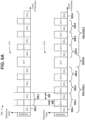
- Fig. 1 is a diagram of an overview of an example implementation 100 described herein.
- a multispectral filter 105 e.g., a binary structure optical filter array
- first mirror 110-1 and second mirror 110-2 may sandwich spacer 120.
- spacer 120 may separate first mirror 110-1 and second mirror 110-2 by a threshold distance, and/or faces of spacer 120 may be enclosed by first mirror 110-1 and second mirror 110-2.
- mirrors 110 may be associated with a particular material.
- mirrors 110 may include a set of dielectric mirror layers (e.g., alternating hydrogenated silicon layers and silicon dioxide layers) or the like to reflect a portion of light directed from a light source toward sensor elements associated with multispectral filter 105.
- Mirrors 110 may align with each sensor element of a sensor element array associated with each channel of multispectral filter 105.
- spacer 120 may include one or more spacer layers 130.
- spacer 120 may include a set of spacer layers 130-1 through 130-5 (e.g., dielectric layers, such as hydrogenated silicon layers).
- a thickness of one or more spacer layers 130 may be associated with ensuring a minimum spacer thickness for a particular wavelength.
- spacer 120 may be associated with a single cavity configuration. Additionally, or alternatively, spacer 120 may be associated with a multicavity configuration.
- a thickness of one or more spacer layers 130 may be related based on a binary progression.
- spacer layer 130-3 may be associated with a thickness of approximately half a thickness of spacer layer 130-2
- spacer layer 130-4 may be associated with a thickness of approximately half the thickness of spacer layer 130-3
- spacer layer 130-5 may be associated with a thickness of approximately half the thickness of spacer layer 130-4.
- multispectral filter 105 may be deposited onto a substrate associated with an optical sensor device.
- mirror 110-1 may be deposited (e.g., via a deposition process and/or a photolithographic lift-off process) onto a substrate that includes an array of sensor elements to capture information (e.g., spectral data).
- spacer 120 may permit capture of information relating to multiple wavelengths. For example, a first portion of spacer 120 aligned with a first sensor element (e.g., a back illuminated optical sensor or a front illuminated optical sensor of a sensor element array) may be associated with a first thickness and a second portion of spacer 120 aligned with a second sensor element may be associated with a second thickness.
- multispectral filter 105 permits multispectral sensing by an optical sensor device using a spacer (e.g., spacer 120) associated with multiple portions, which are associated with multiple thicknesses, aligned to multiple sensor elements of the optical sensor device.
- spacer e.g., spacer 120
- Fig. 1 is provided merely as an example. Other examples are possible and may differ from what was described with regard to Fig. 1 .
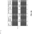
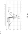
- Figs. 2A-2D are diagrams of characteristics relating to a multispectral filter.
- Figs. 2A-2D show an example of a multispectral filter with a first set of two quarterwave stacks and a second set of two quarterwave stacks sandwiching a spacer.
- the hydrogenated silicon layers of the first quarterwave stack and the second quarterwave stack may each be associated with a refractive index of approximately 3.7226 at a spectral range of approximately 932 nm, a physical thickness of approximately 62.6 nm, and a quarterwave optical thickness (shown as "Q.W.O.T.") of approximately 932 nm.
- Quarterwave optical thickness of a layer corresponds to the physical thickness and refractive index of the layer.
- the high index layers of the quarterwave stacks e.g., the hydrogenated silicon layers, which are associated with a higher index than the low-index layers of the quarterwave stack-the silicon dioxide layers
- the high index layers may be associated with a refractive index, at a spectral range of approximately 800 nm to approximately 1100 nm, that is greater than approximately 2.0, approximately 2.5, approximately 3.0, approximately 3.5, approximately 3.6, approximately 3.7, or the like.
- a difference between a refractive index of the high index material layers and a refractive index of the low index material layers may be greater than a threshold, such as greater than approximately 1.0, greater than approximately 1.5, greater than approximately 2.0, or the like.
- the silicon dioxide layers of the first set of two quarterwave stacks and the second set of two quarterwave stacks may each be associated with a refractive index of approximately 1.4664 at a spectral range of approximately 932 nm, a physical thickness of approximately 158.9 nm, and a quarterwave optical thickness of approximately 932 nm.
- the low index layers of the quarterwave stacks may be associated with a refractive index less than a threshold value at a spectral range of approximately 800 nm to approximately 1100 nm, such as a refractive index less than the refractive index of the high index layers, less than approximately 3.0, less than approximately 2.5, less than approximately 2.0, less than approximately 1.75, less than approximately 1.5, or the like.
- the hydrogenated silicon spacer layer is associated with a refractive index of approximately 3.7226, a physical thickness of approximately 125.2 nm, and a quarterwave optical thickness of approximately 1864 nm.
- the hydrogenated silicon spacer layer may include multiple spacer layers of hydrogenated silicon of multiple thicknesses selected to form multiple channels.
- the hydrogenated silicon spacer layer may be formed using multiple layers to form 64 channels.
- the hydrogenated silicon spacer layer may be formed using multiple layers to form 128 channels.
- a spacer layer may be utilized to form another threshold quantity of channels, such as 8 channels, 16 channels, 32 channels, 256 channels, or the like.
- the spacer layer may be associated with a refractive index greater than a threshold at a spectral range of approximately 800 nm to approximately 1100 nm, such as a refractive index greater than approximately 2.0, approximately 2.5, approximately 3.0, approximately 3.5, approximately 3.6, approximately 3.7, or the like.
- filter 210 is associated with a transmissivity (shown as "T[%]”) of greater than approximately 90% at a wavelength (shown as " ⁇ [nm]”) of approximately 932 nm.
- filter 210 is associated with a relative 50% bandwidth (e.g., a bandwidth for transmissivity greater than 50% surrounding a center wavelength representing a peak transmissivity) of approximately 5.3 nm in a spectral range from approximately 929.35 nm to approximately 934.65 nm.
- FIGS. 2A-2D are provided merely as examples. Other examples are possible and may differ from what was described with regard to Figs. 2A-2D .
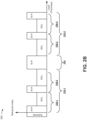
- Figs. 3A-3D are diagrams of characteristics relating to a multispectral filter.
- Figs. 3A-3D show an example of a multispectral filter with a first set of three quarterwave stacks and a second set of three quarterwave stacks sandwiching a spacer.
- chart 350 represents a refractive index profile of a filter 310.
- filter 310 includes a substrate, a first mirror 352-1 deposited on the substrate, a second mirror 352-2, and a hydrogenated silicon spacer 354 disposed between first mirror 352-1 and second mirror 352-2.
- First mirror 352-1 includes a set of three quarterwave stacks 356-1 through 356-3.
- Second mirror 352-2 includes a set of three quarterwave stacks 356-4 through 356-6.
- Each quarterwave stack 356 includes a hydrogenated silicon layer and a silicon dioxide layer forming an HL pair.
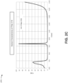
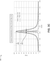
- the filter response for filter 210 and a filter response for filter 310 are provided.
- filter 310 is associated with a reduced peak transmissivity and a reduced relative 50% bandwidth. In this case, as shown in Fig.
- filter 210 is associated with a transmissivity of approximately 92% at approximately 932 nm and a 50% relative bandwidth of 5.3 nm.
- filter 310 is associated with a peak transmissivity of approximately 76% at approximately 932 nm, and is associated with a 50% relative bandwidth of approximately 0.9 nm.
- filter 310 is associated with a reduced out of band transmission relative to filter 210, and a minimum transmissivity is reduced from approximately 0.1% to approximately 0.005% for filter 310 relative to filter 210.
- transmissivity for filter 310 may be further improved by matching a configuration of filter 310 to a substrate and another medium (e.g., air).
- a quantity of quarterwave stacks in mirrors of a multispectral filter causes a change to optical characteristics of the multispectral filter, thereby enabling tuning the multispectral filter for a particular spectral range, a particular transmissivity, or the like.
- the change in optical characteristics may be greater than a threshold change.
- a multispectral filter may be desired that is associated with a 50% relative bandwidth that is between approximately 0.9 nm and approximately 5.3 nm.
- FIGS. 3A-3D are provided merely as examples. Other examples are possible and may differ from what was described with regard to Figs. 3A-3D .
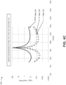
- Figs. 4A-4C are diagrams of characteristics relating to a multispectral filter.
- Figs. 4A-4C show an example of a multispectral filter with an additional low index layer (e.g., a silicon dioxide layer) disposed contiguous to each of a first set of three quarterwave stacks and a second set of three quarterwave stacks, and a spacer disposed between the first set of three quarter wave stacks, the second set of three quarterwave stacks, and the additional low index layers.
- an additional low index layer e.g., a silicon dioxide layer
- chart 450 represents a refractive index profile of a filter 410.
- filter 410 includes a substrate, a first mirror 452-1 deposited on the substrate, a second mirror 452-2, and a spacer 454 disposed between first mirror 452-1 and second mirror 452-2.
- First mirror 452-1 includes a set of quarterwave stacks 456-1 through 456-3 and an unpaired silicon dioxide layer 458-1 (e.g., a low index silicon dioxide layer not paired with a high index hydrogenated silicon layer or another high index layer).
- second mirror 452-2 includes a set of quarterwave stacks 456-4 through 456-6 and an unpaired silicon dioxide layer 458-2.
- Each quarterwave stack 456 is disposed between unpaired silicon dioxide layers 458-1 and 458-2, and includes a hydrogenated silicon layer and a silicon dioxide layer forming an HL pair. Although silicon dioxide layers 458 are not paired with corresponding high index layers (e.g., hydrogenated silicon layers), each silicon dioxide layer 458 may be termed a quarterwave stack for a respective mirror 452.
- filter 410 may be an array of optical filters aligned to a set of sensor elements of a sensor element array.
- a set of filter responses for filter 210, filter 310, and filter 410 is provided.
- filter 410 is associated with a peak transmissivity at approximately 932 nm that is between that of filter 210 and filter 310, and a 50% relative bandwidth that is between that of filter 210 and filter 310. In this case, as shown in Fig.
- filter 210 is associated with a peak transmissivity of greater than 90% at approximately 932 nm and is associated with a 50% relative bandwidth of approximately 5.3 nm.
- filter 310 is associated with a peak transmissivity of approximately 75% at approximately 932 nm and a 50% relative bandwidth of approximately 0.9 nm.
- filter 410 is associated with a peak transmissivity of approximately 80% at approximately 932 nm and a 50% relative bandwidth of approximately 1.4 nm.
- adding the unpaired set of silicon dioxide layers causes a change to optical characteristics of a multispectral filter, thereby enabling tuning the multispectral filter for a particular spectral range, a particular transmissivity, a particular bandwidth, or the like with a greater granularity than altering a quantity of quarterwave stacks.
- FIGS. 4A-4C are provided merely as examples. Other examples are possible and may differ from what was described with regard to Figs. 4A-4C .
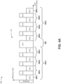
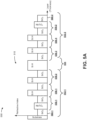
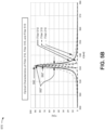
- Figs. 5A-5C are diagrams of characteristics relating to a multispectral filter.
- Figs. 5A-5C show an example of a multispectral filter with mixed sets of quarterwave stacks, and a spacer disposed between the mixed sets of quarterwave stacks.
- chart 550 represents a refractive index profile of a filter 510.
- filter 510 includes a substrate, a first mirror 552-1 deposited on the substrate, a second mirror 552-2, and a spacer 554 disposed between first mirror 552-1 and second mirror 552-2.
- First mirror 552-1 includes a set of quarterwave stacks 556-1 and 556-2, a quarterwave stack 558-1, and an unpaired silicon dioxide layer 560-1.
- second mirror 552-2 includes a set of quarterwave stacks 556-3 and 556-4, a quarterwave stack 558-2, and an unpaired silicon dioxide layer 560-2.
- Each quarterwave stack 556 includes hydrogenated silicon and silicon dioxide forming an HL pair.
- Each quarterwave stack 558 includes niobium titanium oxide (NbTiO x ) forming an HL pair.
- filter 510 utilizes mixed sets of quarterwave stacks, with each mirror 552 including different types of HL pairs. Utilization of the mixed sets of quarterwave stacks permits characteristics of filter 510 to be controlled with a greater granularity than another technique that utilizes increased or decreased quantities of quarterwave stacks to control characteristics.
- niobium titanium oxide, silicon dioxide, and hydrogenated silicon for quarterwave stacks of filter 510
- filter response for filter 210 As shown in Fig. 5B , and by chart 570; and in Fig. 5C , and by chart 580, the filter response for filter 210, the filter response for filter 310, and a filter response for filter 510 are provided.
- filter 510 is associated with a peak transmissivity at approximately 932 nm and a 50% relative bandwidth that is between that of filter 210 and filter 310. In this case, as shown in Fig.
- filter 210 is associated with a peak transmissivity of greater than 90% at approximately 932 nm and a 50% relative bandwidth of approximately 5.3 nm
- filter 310 is associated with a peak transmissivity of approximately 75% at approximately 932 nm and a 50% relative bandwidth of approximately 0.9 nm
- filter 510 is associated with a peak transmissivity of approximately 90% at approximately 932 nm and a 50% relative bandwidth of approximately 3.1 nm.
- utilizing the set of mixed quarterwave stacks causes a change to optical characteristics of the multispectral filter, thereby enabling tuning the multispectral filter for a particular spectral range, a particular transmissivity, or the like with a greater granularity than altering a quantity of quarterwave stacks.
- FIGS. 5A-5C are provided merely as examples. Other examples are possible and may differ from what was described with regard to Figs. 5A-5C .
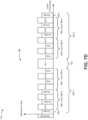
- Figs. 6A-6C are diagrams of characteristics relating to a multispectral filter.
- Figs. 6A-6C show an example of a multispectral filter with detuned sets of quarterwave stacks, and a spacer disposed between the detuned sets of quarterwave stacks.
- chart 650 represents a comparison of a refractive index profile of filter 410 and a refractive index profile of a filter 610.
- filter 610 includes a substrate, a first mirror 652-1 deposited on the substrate, a second mirror 652-2, and a hydrogenated silicon spacer 654 disposed between first mirror 652-1 and second mirror 652-2.
- First mirror 652-1 includes a set of quarterwave stacks 656-1 through 656-3 and an unpaired silicon dioxide layer 658-1.
- second mirror 652-2 includes a set of quarterwave stacks 656-4 through 656-6 and an unpaired silicon dioxide layer 658-2.
- Each quarterwave stack 656 includes a hydrogenated silicon layer and a silicon dioxide layer forming an HL pair.
- another set of materials may be used for quarterwave stacks 656.
- quarterwave stacks 656 may be a mixed set of quarterwave stacks using three or more materials.
- filter 610 (e.g., of mirrors 652) includes silicon dioxide layers that are associated with a threshold reduction in thickness relative to silicon dioxide layers of filter 410 (e.g., of mirrors 452). As shown by reference number 662, filter 610 includes hydrogenated silicon layers associated with a threshold increase in thickness relative to hydrogenated silicon layers of filter 410.
- the threshold increase or reduction may be a selected to detune the quarterwave stacks from a quarterwave thickness (e.g., a thickness associated with a center wavelength of light that is to be incident on the quarterwave stacks), thereby centering filter 610 at a selected center wavelength for a peak transmissivity and/or altering a 50% relative bandwidth for filter 610, such as by utilizing an approximately 30% increase or an approximately 30% reduction in thickness. Additionally, or alternatively, an increase or reduction in thickness between approximately 25% and 30%, between approximately 20% and 40%, between approximately 10% and 50%, or the like may be selected for filter 610.
- a quarterwave thickness e.g., a thickness associated with a center wavelength of light that is to be incident on the quarterwave stacks
- an increase or reduction in thickness between approximately 25% and 30%, between approximately 20% and 40%, between approximately 10% and 50%, or the like may be selected for filter 610.
- a set of filter responses for filter 210, filter 310, and filter 610 is provided.
- filter 610 is associated with a peak transmissivity at approximately 932 nm and a 50% relative bandwidth that is between that of filter 210 and filter 310.
- filter 610 is associated with a peak transmissivity at approximately 932 nm and a 50% relative bandwidth that is between that of filter 210 and filter 310.
- filter 210 is associated with a peak transmissivity of greater than 90% at approximately 932 nm and a 50% relative bandwidth of approximately 5.3
- filter 310 is associated with a peak transmissivity of approximately 75% at approximately 932 nm and a 50% relative bandwidth of approximately 0.9 nm
- filter 610 is associated with a peak transmissivity of approximately 87% at approximately 932 nm and a 50% relative bandwidth of approximately 2.0 nm.
- utilizing the set of detuned quarterwave stacks causes a change to optical characteristics of the multispectral filter, thereby enabling tuning the multispectral filter for a particular spectral range, a particular transmissivity, or the like with a greater granularity than altering a quantity of quarterwave stacks.
- detuning a thickness of quarterwave stacks permits configuration of an optical filter with a selected bandwidth, such as a bandwidth between bandwidths associated with different quantities of quarterwave stacks, a bandwidth overlapping with bandwidths associated with different quantities of quarterwave stacks, or the like.
- FIGS. 6A-6C are provided merely as examples. Other examples are possible and may differ from what was described with regard to Figs. 6A-6C .
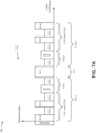
- Figs. 7A-7D are diagrams of characteristics relating to a set of multispectral filters.
- Figs. 7A-7D show examples of multispectral filters with mixed sets of quarterwave stacks.
- chart 705 represents a refractive index profile of filter 710.
- filter 710 includes a substrate, a first mirror 712-1 deposited on the substrate, a second mirror 712-2, and a hydrogenated silicon spacer 714 disposed between first mirror 712-1 and second mirror 712-2.
- First mirror 712-1 includes a set of quarterwave stacks 716-1 and 716-2 of hydrogenated silicon and silicon dioxide as HL pairs and a quarterwave stack 718-1 of niobium titanium oxide and silicon dioxide as an HL pair.
- Second mirror 712-2 includes a set of quarterwave stacks 716-3 and 716-4 of hydrogenated silicon and silicon dioxide as HL pairs and a quarterwave stack 718-2 of niobium titanium oxide and silicon dioxide as an HL pair.
- quarterwave stack 718-1 is disposed between quarterwave stack 716-2 and hydrogenated silicon spacer 714
- quarterwave stack 718-2 is disposed between quarterwave stack 716-3 and hydrogenated silicon spacer 714.
- chart 735 represents a refractive index profile of filter 740.
- filter 740 includes a substrate, a first mirror 742-1 deposited onto the substrate, a second mirror 742-2, and a hydrogenated silicon spacer 744 disposed between first mirror 742-1 and second mirror 742-2.
- First mirror 742-1 includes a set of quarterwave stacks 746-1 and 746-2 of hydrogenated silicon and silicon dioxide as HL pairs, a quarterwave stack 748-1 of niobium titanium oxide and silicon dioxide as an HL pair, and an unpaired silicon dioxide layer 750-1.
- second mirror 762-2 includes a quarterwave stack 766-2 of hydrogenated silicon and tantalum pentoxide as an HL pair, a set of two quarterwave stacks 768-3 and 768-4 of hydrogenated silicon and silicon dioxide as HL pairs, and an unpaired tantalum pentoxide layer 770-2.
- quarterwave stacks 768-1 and 768-2 are disposed between quarterwave stack 766-1 and hydrogenated silicon spacer 764
- quarterwave stacks 768-3 and 768-4 are disposed between quarterwave stack 766-2 and hydrogenated silicon spacer 764.
- second mirror 782-2 includes a set of two quarterwave stacks 786-3 and 786-4 of hydrogenated silicon and niobium titanium oxide as HL pairs, a set of two quarterwave stacks 788-3 and 788-4 of hydrogenated silicon and silicon dioxide as HL pairs, and an unpaired tantalum pentoxide layer 790-2.
- quarterwave stacks 788-1 and 788-2 are disposed between quarterwave stack 786-2 and hydrogenated silicon spacer 784
- quarterwave stacks 788-3 and 788-4 are disposed between quarterwave stack 786-3 and hydrogenated silicon spacer 784.
- FIGS. 7A-7D are provided merely as examples. Other examples are possible and may differ from what was described with regard to Figs. 7A-7D .
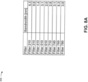
- Figs. 8A and 8B are diagrams of characteristics relating to a set of multispectral filters. Figs. 8A and 8B show examples of 50% relative bandwidths for filters described herein.
- a set of 50% relative bandwidths for filters described herein is provided for a center wavelength of approximately 932 nm.
- filter 210 is associated with a 50% relative bandwidth of approximately 5.3 nm.
- Adding an additional quarterwave stack to form filter 310 results in a 50% relative bandwidth of approximately 0.9 nm.
- multiple techniques may be utilized to tune a multispectral filter with a greater degree of granularity (e.g., to tune a multispectral filter to a 50% relative bandwidth that is between approximately 0.9 nm and approximately 5.3 nm or another range of 50% relative bandwidths associated with another set of multispectral filters).
- filter 410 results in a 50% relative bandwidth of approximately 1.4 nm
- filter 510 results in a relative bandwidth of approximately 3.1 nm
- filter 610 results in a 50% relative bandwidth of 2.0 nm
- filter 710 results in a 50% relative bandwidth of approximately 2.8 nm
- filter 740 results in a 50% relative bandwidth of approximately 3.1 nm
- filter 760 results in a 50% relative bandwidth of approximately 5.3 nm
- filter 780 results in a 50% relative bandwidth of approximately 3.0 nm.
- a multispectral filter may utilize three or more different materials for quarterwave stack mirrors, detuned quarterwave stack thicknesses, unpaired quarterwave stack layers, or the like to achieve a particular spectral range, transmissivity, or the like.
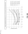
- a set of 50% relative bandwidths for filters described herein is provided at a set of center wavelengths. For example, based on tuning a multispectral filter described herein to a particular center wavelength (e.g., by altering a spacer thickness for the multispectral filter), a 50% relative bandwidth may be determined. As shown, for a spectral range of center wavelengths of between approximately 800 nm and approximately 1100 nm, each of filters 410, 510, 610, 710, 740, 760, and 780 is associated with a 50% relative bandwidth between that of filters 210 and 310.
- filters 410, 510, 610, 710, 740, 760, and 780 are associated with a 50% relative bandwidth of between approximately 3.75 nm and approximately 5.75 nm.
- filters 410, 510, 610, 710, 740, 760, and 780 are associated with a 50% relative bandwidth of between approximately 4 nm and approximately 8 nm.
- FIGS. 8A and 8B are provided merely as examples. Other examples are possible and may differ from what was described with regard to Figs. 8A and 8B .
- utilizing a third coating material, fourth coating material, or the like or detuning a thickness of quarterwave stacks may permit improve granularity of tuning of an optical filter for a particular spectral range, transmissivity, or the like relative to an addition or subtraction of one quarterwave stack, an addition or subtraction of two quarterwave stacks, an addition or subtraction of three quarterwave stacks, an addition or subtraction of four quarterwave stacks, or the like.
- satisfying a threshold may refer to a value being greater than the threshold, more than the threshold, higher than the threshold, greater than or equal to the threshold, less than the threshold, fewer than the threshold, lower than the threshold, less than or equal to the threshold, equal to the threshold, etc.
Landscapes
- Physics & Mathematics (AREA)
- General Physics & Mathematics (AREA)
- Optics & Photonics (AREA)
- Spectroscopy & Molecular Physics (AREA)
- Optical Filters (AREA)
- Spectrometry And Color Measurement (AREA)
- Solid State Image Pick-Up Elements (AREA)
- Separation By Low-Temperature Treatments (AREA)
- Filtration Of Liquid (AREA)
- Control Of Motors That Do Not Use Commutators (AREA)
Applications Claiming Priority (2)
| Application Number | Priority Date | Filing Date | Title |
|---|---|---|---|
| US15/601,753 US10782460B2 (en) | 2017-05-22 | 2017-05-22 | Multispectral filter |
| EP18170865.2A EP3407104B1 (de) | 2017-05-22 | 2018-05-04 | Multispektraler filter |
Related Parent Applications (3)
| Application Number | Title | Priority Date | Filing Date |
|---|---|---|---|
| EP18170865.2A Division-Into EP3407104B1 (de) | 2017-05-22 | 2018-05-04 | Multispektraler filter |
| EP18170865.2A Division EP3407104B1 (de) | 2017-05-22 | 2018-05-04 | Multispektraler filter |
| EP18170865.2A Previously-Filed-Application EP3407104B1 (de) | 2017-05-22 | 2018-05-04 | Multispektraler filter |
Publications (2)
| Publication Number | Publication Date |
|---|---|
| EP4582840A2 true EP4582840A2 (de) | 2025-07-09 |
| EP4582840A3 EP4582840A3 (de) | 2025-09-03 |
Family
ID=62116741
Family Applications (2)
| Application Number | Title | Priority Date | Filing Date |
|---|---|---|---|
| EP25178335.3A Pending EP4582840A3 (de) | 2017-05-22 | 2018-05-04 | Multispektralfilter |
| EP18170865.2A Active EP3407104B1 (de) | 2017-05-22 | 2018-05-04 | Multispektraler filter |
Family Applications After (1)
| Application Number | Title | Priority Date | Filing Date |
|---|---|---|---|
| EP18170865.2A Active EP3407104B1 (de) | 2017-05-22 | 2018-05-04 | Multispektraler filter |
Country Status (8)
| Country | Link |
|---|---|
| US (3) | US10782460B2 (de) |
| EP (2) | EP4582840A3 (de) |
| JP (1) | JP7059098B2 (de) |
| KR (2) | KR102299519B1 (de) |
| CN (3) | CN119291832A (de) |
| CA (1) | CA3002993A1 (de) |
| HK (1) | HK1256258A1 (de) |
| TW (3) | TWI809511B (de) |
Families Citing this family (13)
| Publication number | Priority date | Publication date | Assignee | Title |
|---|---|---|---|---|
| US10725336B2 (en) * | 2016-05-20 | 2020-07-28 | Sharp Kabushiki Kaisha | Liquid crystal display panel and liquid crystal display device |
| US10782460B2 (en) | 2017-05-22 | 2020-09-22 | Viavi Solutions Inc. | Multispectral filter |
| US11143803B2 (en) * | 2018-07-30 | 2021-10-12 | Viavi Solutions Inc. | Multispectral filter |
| US11137331B2 (en) | 2018-08-21 | 2021-10-05 | Viavi Solutions Inc. | Multispectral sensor based alert condition detector |
| US11650361B2 (en) * | 2018-12-27 | 2023-05-16 | Viavi Solutions Inc. | Optical filter |
| US11314004B2 (en) * | 2019-04-08 | 2022-04-26 | Visera Technologies Company Limited | Optical filters and methods for forming the same |
| CN110082849A (zh) * | 2019-06-05 | 2019-08-02 | 信阳舜宇光学有限公司 | 近红外窄带滤光片及制作方法 |
| US11789188B2 (en) * | 2019-07-19 | 2023-10-17 | Viavi Solutions Inc. | Optical filter |
| KR20210014491A (ko) * | 2019-07-30 | 2021-02-09 | 삼성전자주식회사 | 광 필터 및 이를 포함하는 분광기 |
| TWI706169B (zh) * | 2019-08-15 | 2020-10-01 | 晶瑞光電股份有限公司 | 紅外帶通濾波結構及應用該結構之紅外帶通濾波器 |
| CN110989049A (zh) * | 2019-10-12 | 2020-04-10 | 信利光电股份有限公司 | 一种红外光高透过率的薄膜及其制备方法和应用 |
| EP4154314A1 (de) * | 2020-05-18 | 2023-03-29 | University of Rochester | Cmos-sensor mit multispektraler bildgebung |
| CN114500894A (zh) | 2020-10-27 | 2022-05-13 | 三星电子株式会社 | 光谱滤波器、包括光谱滤波器的图像传感器和电子设备 |
Family Cites Families (39)
| Publication number | Priority date | Publication date | Assignee | Title |
|---|---|---|---|---|
| JPH08508114A (ja) | 1993-12-23 | 1996-08-27 | ハネウエル・インコーポレーテッド | カラーフィルタ・アレイ |
| US5926317A (en) * | 1996-11-06 | 1999-07-20 | Jds Fitel Inc. | Multilayer thin film dielectric bandpass filter |
| CA2285466A1 (en) | 1998-01-15 | 1999-07-22 | Ciena Corporation | Optical interference filter |
| GB9901858D0 (en) | 1999-01-29 | 1999-03-17 | Secr Defence | Optical filters |
| EP1088248A1 (de) | 1999-04-20 | 2001-04-04 | Ciena Corporation | Doppeluebertragungsband-interferenzfilter |
| TW528891B (en) * | 2000-12-21 | 2003-04-21 | Ind Tech Res Inst | Polarization-independent ultra-narrow bandpass filter |
| TW520447B (en) * | 2001-05-23 | 2003-02-11 | Univ Tsinghua | Interference filter |
| US20030087121A1 (en) * | 2001-06-18 | 2003-05-08 | Lawrence Domash | Index tunable thin film interference coatings |
| KR20040035708A (ko) * | 2001-08-02 | 2004-04-29 | 이지스 세미컨덕터 | 가변형 광학기기 |
| US6865315B2 (en) | 2001-08-29 | 2005-03-08 | Jds Uniphase Corporation | Dispersion compensating filters |
| JP4028219B2 (ja) | 2001-12-11 | 2007-12-26 | 日本電信電話株式会社 | 光学多層膜フィルタ |
| US6963685B2 (en) * | 2002-07-09 | 2005-11-08 | Daniel Mahgerefteh | Power source for a dispersion compensation fiber optic system |
| US6850366B2 (en) * | 2002-10-09 | 2005-02-01 | Jds Uniphase Corporation | Multi-cavity optical filter |
| TWI298582B (en) * | 2002-10-25 | 2008-07-01 | Hon Hai Prec Ind Co Ltd | Thin film filter for dense wavelength division multiplexing |
| JP2007514961A (ja) * | 2003-10-07 | 2007-06-07 | アイギス セミコンダクター インコーポレイテッド | Cteが一致する透明基板上にヒータを有する調整可能な光フィルタ |
| JP4401880B2 (ja) * | 2004-07-09 | 2010-01-20 | 光伸光学工業株式会社 | 多重バンドパスフィルタ |
| CN100419471C (zh) * | 2005-08-02 | 2008-09-17 | 中山大学 | 一种多频锐角空间滤光片 |
| WO2007082202A2 (en) * | 2006-01-09 | 2007-07-19 | Chemimage Corporation | Birefringent spectral filter with wide field of view and associated communications method and apparatus |
| CN101038373A (zh) * | 2006-03-13 | 2007-09-19 | 爱普生拓优科梦株式会社 | 偏振光分离元件及其制造方法 |
| US7378346B2 (en) * | 2006-03-22 | 2008-05-27 | Motorola, Inc. | Integrated multi-wavelength Fabry-Perot filter and method of fabrication |
| WO2008108784A2 (en) | 2006-05-23 | 2008-09-12 | Regents Of The Uninersity Of Minnesota | Tunable finesse infrared cavity thermal detectors |
| US7903338B1 (en) * | 2006-07-08 | 2011-03-08 | Cirrex Systems Llc | Method and system for managing light at an optical interface |
| DE102007025600B4 (de) * | 2007-05-31 | 2009-05-28 | Schott Ag | Interferenzfilter und Verfahren zu dessen Herstellung |
| US8072402B2 (en) * | 2007-08-29 | 2011-12-06 | Qualcomm Mems Technologies, Inc. | Interferometric optical modulator with broadband reflection characteristics |
| RU2012101436A (ru) | 2009-06-17 | 2013-07-27 | Конинклейке Филипс Электроникс Н.В. | Интерференционные фильтры с высоким пропусканием и широким диапазоном подавления для мини-спектрометра |
| US20140247481A1 (en) | 2011-09-20 | 2014-09-04 | Jenoptik Optical Systems Gmbh | Optical component for the ir range with stress-compensated coating |
| JP5873355B2 (ja) | 2012-02-29 | 2016-03-01 | 三ツ星ベルト株式会社 | シームレスベルト |
| JP2013190652A (ja) * | 2012-03-14 | 2013-09-26 | Toshiba Corp | 液晶表示装置 |
| TWI855290B (zh) * | 2012-07-16 | 2024-09-11 | 美商唯亞威方案公司 | 光學濾波器及感測器系統 |
| JP6272627B2 (ja) * | 2013-01-29 | 2018-01-31 | ヴァイアヴィ・ソリューションズ・インコーポレイテッドViavi Solutions Inc. | 可変光学フィルターおよびそれに基づく波長選択型センサー |
| CN103984054B (zh) * | 2014-05-16 | 2017-04-12 | 中国科学院上海光学精密机械研究所 | 全介质f‑p窄带消偏振滤光片 |
| EP3158371B1 (de) * | 2014-06-18 | 2025-04-23 | Viavi Solutions Inc. | Herstellungsverfahren für ein optischen metall-dielektrischen filter |
| JP6542511B2 (ja) | 2014-06-30 | 2019-07-10 | Agc株式会社 | 帯域透過フィルタ |
| JP6137135B2 (ja) * | 2014-11-20 | 2017-05-31 | トヨタ自動車株式会社 | 車両の駆動制御装置 |
| KR102758126B1 (ko) | 2015-01-23 | 2025-01-21 | 마테리온 코포레이션 | 개선된 투과를 갖는 근적외선 광학 간섭 필터 |
| US20180170093A1 (en) | 2015-06-30 | 2018-06-21 | Spectral Devices Inc. | Flexible pixelated fabry-perot filter |
| US9923007B2 (en) * | 2015-12-29 | 2018-03-20 | Viavi Solutions Inc. | Metal mirror based multispectral filter array |
| US10782460B2 (en) | 2017-05-22 | 2020-09-22 | Viavi Solutions Inc. | Multispectral filter |
| CN108333661B (zh) * | 2018-03-13 | 2024-01-02 | 湖北五方光电股份有限公司 | 基于硼掺杂氢化硅的低角度偏移滤光片及其制备方法 |
-
2017
- 2017-05-22 US US15/601,753 patent/US10782460B2/en active Active
-
2018
- 2018-04-27 JP JP2018087610A patent/JP7059098B2/ja active Active
- 2018-04-27 CA CA3002993A patent/CA3002993A1/en active Pending
- 2018-05-01 TW TW110135642A patent/TWI809511B/zh active
- 2018-05-01 TW TW112125273A patent/TWI864865B/zh active
- 2018-05-01 TW TW107114782A patent/TWI744528B/zh active
- 2018-05-04 EP EP25178335.3A patent/EP4582840A3/de active Pending
- 2018-05-04 EP EP18170865.2A patent/EP3407104B1/de active Active
- 2018-05-21 KR KR1020180057691A patent/KR102299519B1/ko active Active
- 2018-05-22 CN CN202411684690.7A patent/CN119291832A/zh active Pending
- 2018-05-22 CN CN202111322234.4A patent/CN114137646B/zh active Active
- 2018-05-22 CN CN201810494349.3A patent/CN109061786B/zh active Active
- 2018-11-29 HK HK18115315.6A patent/HK1256258A1/en unknown
-
2020
- 2020-08-27 US US16/948,003 patent/US11880054B2/en active Active
-
2021
- 2021-09-01 KR KR1020210116358A patent/KR102602452B1/ko active Active
-
2023
- 2023-12-11 US US18/534,780 patent/US20240103210A1/en active Pending
Also Published As
| Publication number | Publication date |
|---|---|
| EP3407104B1 (de) | 2025-07-02 |
| US20240103210A1 (en) | 2024-03-28 |
| EP3407104A1 (de) | 2018-11-28 |
| US10782460B2 (en) | 2020-09-22 |
| KR102602452B1 (ko) | 2023-11-15 |
| CN114137646B (zh) | 2024-12-03 |
| KR20180127931A (ko) | 2018-11-30 |
| US11880054B2 (en) | 2024-01-23 |
| TW201901195A (zh) | 2019-01-01 |
| EP3407104C0 (de) | 2025-07-02 |
| JP7059098B2 (ja) | 2022-04-25 |
| TW202204941A (zh) | 2022-02-01 |
| TWI864865B (zh) | 2024-12-01 |
| CN109061786A (zh) | 2018-12-21 |
| CN114137646A (zh) | 2022-03-04 |
| CA3002993A1 (en) | 2018-11-22 |
| JP2018200464A (ja) | 2018-12-20 |
| TWI809511B (zh) | 2023-07-21 |
| CN109061786B (zh) | 2021-11-26 |
| KR102299519B1 (ko) | 2021-09-07 |
| TW202343039A (zh) | 2023-11-01 |
| TWI744528B (zh) | 2021-11-01 |
| US20200393602A1 (en) | 2020-12-17 |
| KR20210111222A (ko) | 2021-09-10 |
| HK1256258A1 (en) | 2019-09-20 |
| EP4582840A3 (de) | 2025-09-03 |
| US20180335557A1 (en) | 2018-11-22 |
| CN119291832A (zh) | 2025-01-10 |
Similar Documents
| Publication | Publication Date | Title |
|---|---|---|
| EP3407104B1 (de) | Multispektraler filter | |
| EP3182079B1 (de) | Vorrichtung zur optischen messung und verfahren zur herstellung einer vorrichtung zur optischen messung | |
| CN113874689B (zh) | 使用多通道色彩传感器的光谱重建 | |
| US11048097B2 (en) | Multiple band pass liquid crystal tunable filter | |
| US11143803B2 (en) | Multispectral filter | |
| EP3514584A1 (de) | Einfallswinkelbeschränkung für optische filter | |
| EP3407102B1 (de) | Multispektraler filter mit gemischtem abstandshalter | |
| HK40062514A (en) | Multispectral filter | |
| HK40062514B (zh) | 多光谱滤光器 | |
| HK1259464B (zh) | 多光谱滤光器 | |
| HK1259464A1 (en) | Multispectral filter | |
| HK40003793A (en) | Angle of incidence restriction for optical filters |
Legal Events
| Date | Code | Title | Description |
|---|---|---|---|
| PUAI | Public reference made under article 153(3) epc to a published international application that has entered the european phase |
Free format text: ORIGINAL CODE: 0009012 |
|
| STAA | Information on the status of an ep patent application or granted ep patent |
Free format text: STATUS: THE APPLICATION HAS BEEN PUBLISHED |
|
| AC | Divisional application: reference to earlier application |
Ref document number: 3407104 Country of ref document: EP Kind code of ref document: P |
|
| AK | Designated contracting states |
Kind code of ref document: A2 Designated state(s): AL AT BE BG CH CY CZ DE DK EE ES FI FR GB GR HR HU IE IS IT LI LT LU LV MC MK MT NL NO PL PT RO RS SE SI SK SM TR |
|
| REG | Reference to a national code |
Ref country code: DE Ref legal event code: R079 Free format text: PREVIOUS MAIN CLASS: G02B0005280000 Ipc: G02B0005200000 |
|
| PUAL | Search report despatched |
Free format text: ORIGINAL CODE: 0009013 |
|
| AK | Designated contracting states |
Kind code of ref document: A3 Designated state(s): AL AT BE BG CH CY CZ DE DK EE ES FI FR GB GR HR HU IE IS IT LI LT LU LV MC MK MT NL NO PL PT RO RS SE SI SK SM TR |
|
| RIC1 | Information provided on ipc code assigned before grant |
Ipc: G02B 5/20 20060101AFI20250731BHEP Ipc: G02B 5/28 20060101ALI20250731BHEP |