EP4571325A1 - Hall plate current sensor having stress compensation - Google Patents
Hall plate current sensor having stress compensation Download PDFInfo
- Publication number
- EP4571325A1 EP4571325A1 EP24212398.2A EP24212398A EP4571325A1 EP 4571325 A1 EP4571325 A1 EP 4571325A1 EP 24212398 A EP24212398 A EP 24212398A EP 4571325 A1 EP4571325 A1 EP 4571325A1
- Authority
- EP
- European Patent Office
- Prior art keywords
- amplifier
- hall plate
- resistor
- coupled
- temperature
- Prior art date
- Legal status (The legal status is an assumption and is not a legal conclusion. Google has not performed a legal analysis and makes no representation as to the accuracy of the status listed.)
- Pending
Links
Images


Classifications
-
- G—PHYSICS
- G01—MEASURING; TESTING
- G01R—MEASURING ELECTRIC VARIABLES; MEASURING MAGNETIC VARIABLES
- G01R15/00—Details of measuring arrangements of the types provided for in groups G01R17/00 - G01R29/00, G01R33/00 - G01R33/26 or G01R35/00
- G01R15/14—Adaptations providing voltage or current isolation, e.g. for high-voltage or high-current networks
- G01R15/20—Adaptations providing voltage or current isolation, e.g. for high-voltage or high-current networks using galvano-magnetic devices, e.g. Hall-effect devices, i.e. measuring a magnetic field via the interaction between a current and a magnetic field, e.g. magneto resistive or Hall effect devices
- G01R15/202—Adaptations providing voltage or current isolation, e.g. for high-voltage or high-current networks using galvano-magnetic devices, e.g. Hall-effect devices, i.e. measuring a magnetic field via the interaction between a current and a magnetic field, e.g. magneto resistive or Hall effect devices using Hall-effect devices
-
- G—PHYSICS
- G01—MEASURING; TESTING
- G01R—MEASURING ELECTRIC VARIABLES; MEASURING MAGNETIC VARIABLES
- G01R33/00—Arrangements or instruments for measuring magnetic variables
- G01R33/007—Environmental aspects, e.g. temperature variations, radiation, stray fields
- G01R33/0082—Compensation, e.g. compensating for temperature changes
-
- G—PHYSICS
- G01—MEASURING; TESTING
- G01R—MEASURING ELECTRIC VARIABLES; MEASURING MAGNETIC VARIABLES
- G01R33/00—Arrangements or instruments for measuring magnetic variables
- G01R33/02—Measuring direction or magnitude of magnetic fields or magnetic flux
- G01R33/06—Measuring direction or magnitude of magnetic fields or magnetic flux using galvano-magnetic devices
- G01R33/07—Hall effect devices
-
- H—ELECTRICITY
- H10—SEMICONDUCTOR DEVICES; ELECTRIC SOLID-STATE DEVICES NOT OTHERWISE PROVIDED FOR
- H10N—ELECTRIC SOLID-STATE DEVICES NOT OTHERWISE PROVIDED FOR
- H10N59/00—Integrated devices, or assemblies of multiple devices, comprising at least one galvanomagnetic or Hall-effect element covered by groups H10N50/00 - H10N52/00
Definitions
- Hall elements can be used for various sensing applications based on detecting magnetic field changes.
- a typical planar or horizontal Hall effect element is a four-terminal device for which a drive current (a DC current) is passed between two opposing ones of the four terminals and a differential voltage (AC or DC), responsive to a magnetic field (AC or DC), is generated between the other two opposing ones of the four terminals.
- An amplitude of the differential signal i.e., voltage
- a sensitivity e.g., mV per Gauss
- Such devices can be referred to as current driver Hall plates.
- the drive current can be generated with a stable current source or a current sink that uses a stable reference voltage.
- various parameters can cause the sensitivity to magnetic fields of the differential signal to change.
- the Hall effect element itself can experience sensitivity changes.
- the changes in sensitivity of the Hall effect element can result directly from temperature changes.
- temperature can be sensed and the changes in sensitivity with temperature can be corrected.
- the changes in sensitivity of the differential signal can also result from stresses upon a substrate on which the Hall effect element is disposed.
- the stresses may or may not be related to temperature and also may or may not be related to a thermal coefficient of a material of a package used to seal the substrate.
- the stresses and resulting changes in sensitivity may vary from unit to unit in different ways with respect to temperature.
- Example embodiments of the disclosure provide methods and apparatus for a voltage-driven Hall plate sensor having stress compensation.
- stress compensation is provided by vertical and/or lateral "epi" resistors for controlling current, such as I VAR and I CONST of a Gilbert cell.
- temperature stress compensation of a voltage-drive Hall plate sensor is provided by certain current ratios and/or trimming. Voltage-driven Hall plate sensors may have lower noise and require less die area, as compared with conventional current driven Hall plate sensors.
- a voltage driven Hall plate current sensor integrated circuit (IC) package comprises: a die including a Hall plate comprising a lateral epi resistor; a gm amplifier to receive an output voltage from the Hall plate; a front end amplifier to receive an output of the gm amplifier; and a compensation circuit to compensate for stress on the die that affects a resistance of the Hall plate, the compensation circuit including a lateral epi resistor coupled to a temperature-dependent current for compensating for piezoresistive stress in the Hall plate.
- An IC package can further include one or more of the following features: a bandgap circuit to generate the temperature-dependent current for the lateral epi resistor, the lateral epi resistor is coupled to the gm amplifier, the gm amplifier comprises a Gilbert cell, a degeneration resistor coupled to terminals of the Gilbert cell, a vertical epi resistor coupled to a variable current source corresponding to a temperature sensitivity value, wherein the vertical epi resistor is configured to compensate for piezo stress sensitivity of the Hall plate, a DAC to receive and output the temperature sensitivity value, the vertical epi resistor is coupled to the gm amplifier, the DAC is coupled to a temperature dependent current, and/or a back end amplifier coupled to an output of the front end amplifier.
- a bandgap circuit to generate the temperature-dependent current for the lateral epi resistor
- the lateral epi resistor is coupled to the gm amplifier
- the gm amplifier comprises a Gilbert cell, a degeneration resistor coupled to terminals of the Gilbert cell, a vertical epi resist
- a method comprises: employing a die including a Hall plate comprising a lateral epi resistor, wherein the die forms a part of a voltage driven Hall plate current sensor integrated circuit (IC) package; connecting a gm amplifier to receive an output voltage from the Hall plate; connecting a front end amplifier to receive an output of the gm amplifier; and configuring a compensation circuit to compensate for stress on the die that affects a resistance of the Hall plate, wherein the compensation circuit includes a lateral epi resistor coupled to a first temperature dependent current source for compensating for piezoresistive stress in the Hall plate.
- IC voltage driven Hall plate current sensor integrated circuit
- a method can further include one or more of the following features: a bandgap circuit to generate the temperature-dependent current for the lateral epi resistor, the lateral epi resistor is coupled to the gm amplifier, the gm amplifier comprises a Gilbert cell, a degeneration resistor coupled to terminals of the Gilbert cell, a vertical epi resistor coupled to a variable current source corresponding to a temperature sensitivity value, wherein the vertical epi resistor is configured to compensate for piezo stress sensitivity of the Hall plate, a DAC to receive and output the temperature sensitivity value, the vertical epi resistor is coupled to the gm amplifier, the DAC is coupled to a temperature dependent current, and/or a back end amplifier coupled to an output of the front end amplifier.
- a voltage driven Hall plate current sensor integrated circuit (IC) package comprises: a die including a Hall plate comprising a lateral epi resistor; a Gilbert cell including a gm amplifier having inputs to receive a differential output voltage from the Hall plate, a degeneration resistor coupled to terminals of the gm amplifier; a front end amplifier to receive an output of the gm amplifier, wherein first and second feedback resistor are coupled in a feedback configuration for first and second inputs of the front end amplifier; a compensation circuit comprising: a lateral epi resistor RCONST coupled to the gm amplifier via a second current generator active device and to a temperature dependent current ICONST for compensating for piezoresistive stress in the Hall plate; a vertical epi resistor RVAR coupled to the gm amplifier via a first current generator active device and to a DAC configured to receive a temperature sensitivity value; a first reference resistor connected to the first current generator active device via a first amplifier and configured to receive a bandgap temperature dependent current
- An IC package can further include one or more of the following features: the first and second reference resistors are matched for a same temperature, the degeneration resistor and the first and second feedback resistors are a same type, the degeneration resistor and the first and second feedback resistors are matched to achieve a same temperature, a bandgap circuit to provide the temperature dependent current to the DAC, a temperature coefficient of the Gilbert cell is trimmed using a constant k Iptat_denom for coarse signal path trimming, and/or the temperature coefficient of the Gilbert cell is finely trimmed by the temperature sensitivity value at the input of the DAC.
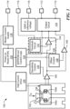
- FIG. 1 shows an example circuit block diagram for a voltage driven Hall plate current sensor integrated circuit 100 having stress compensation in accordance with example embodiments of the disclosure.
- a current I p flows through a current conductor loop 102 and generates a magnetic field that can be sensed by first and second magnetic field sensing elements 104a,b, such as Hall effect plates for example.
- the magnetic field results in the Hall effect plates 104a,b providing a signal to a front-end amplifier 106.
- the front-end amplifier 106 provides an output to amplifier 108, which may be a linear amplifier, which feeds into an output circuit 110.
- Output circuit 110 may be a digital or analog circuit that provides an output to at least one bond pad 112. The output represents the magnetic field measured and amplified through the amplifier 108. Other numbers of output bond pads more than two may also be provided.
- Bond pad 114 provides a voltage and current input, typically Vcc, to provide power to the integrated circuit 100.
- a ground bond pad 116 may be provided to integrated circuit 100.
- Input bond pad 114 is coupled to a master current supply circuit 118 that provides power to the circuitry within integrated circuit 100.
- master current supply 118 is provided as a current supply, it would be apparent that voltages may also be provided to the circuits on integrated circuit 100.
- a Hall effect current drive circuit 120 takes current (or voltage) from the master current supply 118 and provides a regulated or non-regulated voltage to the Hall Effect sensing elements 104a,b.
- the master current supply 118 also provides control signal to a power on reset circuit 122.
- the power on reset circuit monitors the power supply voltage coming into the circuit 100 and provides a signal to EEPROM and control logic circuit 124.
- the power on reset circuit 122 and EEPROM and control logic circuit 124 are used to configure and enable the integrated circuit, including the output circuit 110.
- the EEPROM and control circuit 124 provides a signal to a sensitivity control circuit 126 which provides a signal to the front end amplifier 106 to adjust the sensitivity of the front end amplifier.
- the adjustment may be the result of a change in the power level in the circuit 100, or as a result of a temperature change of the circuit.
- An example of a temperature sensor circuit may include but is not limited to a diode temperature sensor, or the use of known temperature compensation resistors.
- the EEPROM and control circuit 124 provides a signal to an offset control circuit 128.
- the offset control circuit 128 provides a signal to the amplifier 108.
- the offset control circuit 128 allows the circuit 100 to adjust the offset of the amplifier 108 for changes in power or temperature (the temperature compensation circuit is not shown) or a combination of temperature and power changes.
- the offset control circuit 128 may also provide adjustment for other offset sources, such as a stress in the integrated circuit die.
- An input lead 115 may be provided to set a threshold for a fault indication circuit 130 (i.e., provide a fault trip level).
- the input lead 115 provides a fault voltage level.
- the fault indication circuit 130 can include a threshold circuit 132 and a fault comparator 134.
- the EEPROM and control circuit 124 provides an input to the threshold circuit 132.
- the threshold circuit 132 provides a signal to the fault comparator 134, which compares the output of threshold circuit 132 with the output of the front end amplifier 106 to indicate when a fault exists to the output circuit block 110.
- the output circuit generates a fault output at output bond pad 113.
- the fault output may indicate an overcurrent condition in which the current sensed in the current conductor path exceeds a fault trip level, which trip level may be provided in the form of a fault voltage level on bond pad 115.
- the fault allows, in one example, the user of the current sensor package to turn off the current in the primary current path in order to prevent a high current condition in an electrical circuit.
- processing may be implemented in hardware, firmware, software, or a combination thereof.
- Processing may be implemented in computer programs executed on programmable computers/machines that each includes a processor, a storage medium or other article of manufacture that is readable by the processor (including volatile and non-volatile memory and/or storage elements), at least one input device, and one or more output devices.
- Program code may be applied to data entered using an input device to perform processing and to generate output information.
- Hall plate sensors are current driven and use conventional current-drive stress compensation techniques.
- Conventional current driven Hall plate sensors have disadvantages, such as the need for voltage margin for the current source driving the Hall plate, relatively high noise levels, and the need for relatively large amounts of die area, such as for current mirrors.
- FIG. 2 shows a portion of a circuit for a prior art current-driven Hall plate sensor.
- a Hall plate 200 generates an output signal Vsig in response to applied magnetic field B.
- a current mirror 202 is used for current driving of the Hall plate 200.
- An amplifier 204 is used for temperature compensation of the Hall plate 200.
- a temperature dependent V T may be used for coarse temperature compensation of R vepi and current driven Hall plate sensors. Fine temperature compensation is usually performed by a segment processor based on temperature sensor reading.
- FIG. 3 shows an example circuit implementation 300 of stress compensation for a voltage driven Hall plate in a current sensor having a front end module 302 and a backend module 304.
- feedback resistors Rfb(rppgp) are coupled in a feedback configuration of the front end amplifier 310 for the differential signal connection, as shown. It is understood that rppgp refers to a type of resistor.
- the circuit includes a bandgap circuit BG to provide a temperature independent voltage reference which is used to generate a constant temperature independent current I BN5u and current proportional to absolute temperature Iptat5u.
- a voltage difference between first and second diodes operated at different current densities generates a current that is proportional to absolute temperature (PTAT) on a resistor.
- PTAT absolute temperature
- This current is used to generate a voltage in a second resistor.
- This voltage in turn is added to the voltage of one of the junctions. It is understood that any suitable bandgap circuit can be used to meet the needs of a particular application.
- current Iptat5u which is provided to a digital-to-analog converter (DAC) 316, flows through resistor Rref1(rgp) to ground.
- the DAC 316 receives a sensitivity trimming digital word and outputs an analog signal to a first of an amplifier 318.
- a second terminal, e.g., source, of the first current generator active device 312, which is coupled to ground via resistor Rvar(rvepi) is connected to a second input of the amplifier 318.
- the output of the amplifier 318 is coupled to a third terminal, e.g., gate, of the first current generator active device 312.
- stress compensation for the voltage driven Hall plate 306 is based on vertical and lateral epi resistors Rvar(rvepi, Rconst(repi) controlling IVAR and ICONST currents of the Gilbert Cell 308. While current ICONST may be constant for a given temperature, current ICONST varies over temperature. It is understood that stress on die can affect the Hall plate resistance Rhp ( epi ), which comprises a lateral epi resistor. Another lateral epi resistor Rconst(repi) can compensate for stress on the Hall plate, however, it may be desirable to provide temperature compensation for the Hall plate stress compensation. Stress compensation of the voltage driven Hall plate may include sensitivity temperature compensation using current Iptat/(4*Iflat-Iptat) with temperature compensation trimming input to the DAC 316.
- ⁇ Sensitivity Sensitivity 45 % / GPa is an example value based on example current driven Hall plate current sensor IC packages without Hall plate stress compensation with an average stress drift of about 1.2%.
- 24.4%/GPa corresponds to Hall plate changes
- 53.4%/GPa refers to vertical epi resistor changes
- 24.4%/GPa corresponds to lateral epi resistor changes.
- An example embodiment of a voltage driven current sensor having Hall plate stress compensation as ⁇ Sensitivity Sensitivity ⁇ 8.4 % / GPa .
- Sensitivity Vcc ⁇ Rconst epi Rhp epi ⁇ S HP Rvar vepi ⁇ Iptat 5 u 4 ⁇ IBN 5 u ⁇ Iptat 5 u ⁇ Rref 1 rgp Rref 2 rgp ⁇ Rfb rppgp Rdgen rppgp ⁇ G BE
- Elements in the above expression sensitive to package stress include S HP , Rvar(vepi), and Rconst(epi).
- the Hall plate sensitivity piezo hall stress effect S HP is compensated by vertical epi resistor Rvar(vepi) that forms the I var control current.
- this compensation is not 100% with a residual stress sensitivity of -8.4%/GPa (see above) which is about 20% of the package stress sensitivity of the current driven Hall plate without stress compensation with negative sign. This value is comparable with current driven Hall plates with stress compensation.
- an example voltage driven Hall plate current sensor embodiment without stress compensation has a sensitivity stress drift of about 69.4%/GPa.
- parts of the sensitivity expression include compensation of the temperature coefficient used signal path configurations.
- Resistor R const(epi) compensates for the thermal coefficient (TC) of the Hall Plate resistance R HP , both which are lateral n-epi resistors.
- element S HP R var vepi can compensate across temperature by element I ptat 4 ⁇ I BN ⁇ I ptat , where
- R ref1 and R ref2 are resistors of the same type that are matched to guarantee the same temperature.
- the Gilbert cell degeneration resistor R dgen is the same type of resistor as the feedback resistors R fb for the transimpedance amplifier 308.
- resistors R dgen and R fb are matched to achieve the same temperature.
- coarse thermal coefficient trimming can be implemented by adjustment of the sensitivity Temperature Coefficient in the Gilbert cell 308 by modifying sensitivity formula element I ptat 4 ⁇ I BN ⁇ I ptat to I ptat 4 ⁇ I BN ⁇ k Iptat _ denom ⁇ I ptat , where k Iptat_denom is used for coarse signal path Sensitivity TC trimming, which should be roughly flat to have good dynamic conditions in the signal path.
- FIG. 4 shows plots for example values of k Iptat_denom with one substantially flat value emphasized in the figure.
- Fine TC trimming can be implemented on the I VAR current by scaling by sensf_trim into the DAC 316 based on a segment processor calculation using, for example, an internal temperature sensor measurement (not shown).
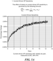
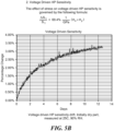
- FIG. 5A shows the effect of stress on a Hall plate sensitivity for a current driven Hall plate and FIG. 5B shows the effect of stress on a Hall plate sensitivity for a voltage-drive Hall plate.
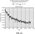
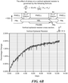
- FIG. 6A shows the effect of stress on a lateral epitaxial resistor and FIG. 6B shows the effect of stress on a vertical epi resistor.
- So-called epi resistors lateral and vertical, are well known in the art of Hall plate sensors.
- Example epi resistors are shown and described for example, in U.S. Patent Nos. 10, 254, 354, and 10,636,285, and 10,520,559, and 10, 746,818 , and U.S. Patent Publication No. 2021/0048353 , all of which are incorporated herein by reference.
- Example embodiments of a voltage drive Hall plate sensor have lower noise than conventional current driven sensors while working at full Vcc to achieve more than 3x lower noise at room temperature.
- voltage driven Hall plate sensors can save significant die area since no die area is needed for current source driving elements in current driven mode for the Hall plate.
- some of the above-described magnetic field sensing elements tend to have an axis of maximum sensitivity parallel to a substrate that supports the magnetic field sensing element, and others of the above-described magnetic field sensing elements tend to have an axis of maximum sensitivity perpendicular to a substrate that supports the magnetic field sensing element.
- planar Hall effect elements tend to have axes of sensitivity perpendicular to a substrate
- metal based or metallic magnetoresistance elements e.g., GMR, TMR, ANM
- vertical Hall effect elements tend to have axes of sensitivity parallel to a substrate.
- magnetic field sensor is used to describe a circuit that uses a magnetic field sensing element, generally in combination with other circuits.
- Magnetic field sensors are used in a variety of applications, including, but not limited to, an angle sensor that senses an angle of a direction of a magnetic field, a current sensor that senses a magnetic field generated by a current carried by a current-carrying conductor, a magnetic switch that senses the proximity of a ferromagnetic object, a rotation detector that senses passing ferromagnetic articles, for example, magnetic domains of a ring magnet or a ferromagnetic target (e.g., gear teeth) where the magnetic field sensor is used in combination with a back-biased or other magnet, and a magnetic field sensor that senses a magnetic field density of a magnetic field.
- an angle sensor that senses an angle of a direction of a magnetic field
- a current sensor that senses a magnetic field generated by a current carried by a current-carrying conductor
- a magnetic switch that
- connections and positional relationships may be used to describe elements in the description and drawing. These connections and/or positional relationships, unless specified otherwise, can be direct or indirect, and the described concepts, systems, devices, structures, and techniques are not intended to be limiting in this respect. Accordingly, a coupling of elements can refer to either a direct or an indirect coupling, and a positional relationship between entities can be a direct or indirect positional relationship.
- positioning element “A” over element “B” can include situations in which one or more intermediate elements (e.g., element “C”) is between elements “A” and elements “B” as long as the relevant characteristics and functionalities of elements “A” and “B” are not substantially changed by the intermediate element(s).
- intermediate elements e.g., element “C”
- Relative or positional terms including, but not limited to, the terms “upper,” “lower,” “right,” “left,” “vertical,” “horizontal, "top,” “bottom,” and derivatives of those terms relate to the described structures and methods as oriented in the drawing figures.
- first element such as a first structure
- second element such as a second structure
- intervening elements such as an interface structure can be present between the first element and the second element.
- direct contact means that a first element, such as a first structure, and a second element, such as a second structure, are connected without any intermediary elements.
- connection can include an indirect “connection” and a direct “connection”.
- references in the specification to "embodiments,” “one embodiment, “an embodiment,” “an example embodiment,” “an example,” “an instance,” “an aspect,” etc., indicate that the embodiment described can include a particular feature, structure, or characteristic, but every embodiment may or may not include the particular feature, structure, or characteristic. Moreover, such phrases are not necessarily referring to the same embodiment. Further, when a particular feature, structure, or characteristic is described in connection with an embodiment, it may affect such feature, structure, or characteristic in other embodiments whether explicitly described or not.
Landscapes
- Physics & Mathematics (AREA)
- General Physics & Mathematics (AREA)
- Condensed Matter Physics & Semiconductors (AREA)
- Health & Medical Sciences (AREA)
- Engineering & Computer Science (AREA)
- Environmental & Geological Engineering (AREA)
- Toxicology (AREA)
- Hall/Mr Elements (AREA)
- Measuring Magnetic Variables (AREA)
Abstract
Methods and apparatus for a voltage driven Hall plate current sensor integrated circuit (IC) package that includes a die including a Hall plate with a lateral epi resistor. A gm amplifier receives an output voltage from the Hall plate and a front end amplifier receives an output of the gm amplifier. A compensation circuit compensates for stress on the die that affects a resistance of the Hall plate and includes a lateral epi resistor coupled to a constant current for compensating for piezoresistive stress in the Hall plate.
Description
- As is known in the art, Hall elements can be used for various sensing applications based on detecting magnetic field changes. A typical planar or horizontal Hall effect element is a four-terminal device for which a drive current (a DC current) is passed between two opposing ones of the four terminals and a differential voltage (AC or DC), responsive to a magnetic field (AC or DC), is generated between the other two opposing ones of the four terminals. An amplitude of the differential signal (i.e., voltage) is related to amplitude of the drive current. Thus, a sensitivity (e.g., mV per Gauss) of the differential signal corresponds to the amplitude of the drive current. Such devices can be referred to as current driver Hall plates.
- In order to maintain a constant and stable sensitivity, the drive current can be generated with a stable current source or a current sink that uses a stable reference voltage. However, various parameters can cause the sensitivity to magnetic fields of the differential signal to change. In general, even with a perfectly stable drive current, the Hall effect element itself can experience sensitivity changes. The changes in sensitivity of the Hall effect element can result directly from temperature changes. In order to correct for this sensitivity change, temperature can be sensed and the changes in sensitivity with temperature can be corrected.
- However, the changes in sensitivity of the differential signal can also result from stresses upon a substrate on which the Hall effect element is disposed. The stresses may or may not be related to temperature and also may or may not be related to a thermal coefficient of a material of a package used to seal the substrate. The stresses and resulting changes in sensitivity may vary from unit to unit in different ways with respect to temperature.
- Example embodiments of the disclosure provide methods and apparatus for a voltage-driven Hall plate sensor having stress compensation. In embodiments, stress compensation is provided by vertical and/or lateral "epi" resistors for controlling current, such as IVAR and ICONST of a Gilbert cell. In embodiments, temperature stress compensation of a voltage-drive Hall plate sensor is provided by certain current ratios and/or trimming. Voltage-driven Hall plate sensors may have lower noise and require less die area, as compared with conventional current driven Hall plate sensors.
- In one aspect, a voltage driven Hall plate current sensor integrated circuit (IC) package comprises: a die including a Hall plate comprising a lateral epi resistor; a gm amplifier to receive an output voltage from the Hall plate; a front end amplifier to receive an output of the gm amplifier; and a compensation circuit to compensate for stress on the die that affects a resistance of the Hall plate, the compensation circuit including a lateral epi resistor coupled to a temperature-dependent current for compensating for piezoresistive stress in the Hall plate.
- An IC package can further include one or more of the following features: a bandgap circuit to generate the temperature-dependent current for the lateral epi resistor, the lateral epi resistor is coupled to the gm amplifier, the gm amplifier comprises a Gilbert cell, a degeneration resistor coupled to terminals of the Gilbert cell, a vertical epi resistor coupled to a variable current source corresponding to a temperature sensitivity value, wherein the vertical epi resistor is configured to compensate for piezo stress sensitivity of the Hall plate, a DAC to receive and output the temperature sensitivity value, the vertical epi resistor is coupled to the gm amplifier, the DAC is coupled to a temperature dependent current, and/or a back end amplifier coupled to an output of the front end amplifier.
- In another aspect, a method comprises: employing a die including a Hall plate comprising a lateral epi resistor, wherein the die forms a part of a voltage driven Hall plate current sensor integrated circuit (IC) package; connecting a gm amplifier to receive an output voltage from the Hall plate; connecting a front end amplifier to receive an output of the gm amplifier; and configuring a compensation circuit to compensate for stress on the die that affects a resistance of the Hall plate, wherein the compensation circuit includes a lateral epi resistor coupled to a first temperature dependent current source for compensating for piezoresistive stress in the Hall plate.
- A method can further include one or more of the following features: a bandgap circuit to generate the temperature-dependent current for the lateral epi resistor, the lateral epi resistor is coupled to the gm amplifier, the gm amplifier comprises a Gilbert cell, a degeneration resistor coupled to terminals of the Gilbert cell, a vertical epi resistor coupled to a variable current source corresponding to a temperature sensitivity value, wherein the vertical epi resistor is configured to compensate for piezo stress sensitivity of the Hall plate, a DAC to receive and output the temperature sensitivity value, the vertical epi resistor is coupled to the gm amplifier, the DAC is coupled to a temperature dependent current, and/or a back end amplifier coupled to an output of the front end amplifier.
- In a further aspect, a voltage driven Hall plate current sensor integrated circuit (IC) package, comprises: a die including a Hall plate comprising a lateral epi resistor; a Gilbert cell including a gm amplifier having inputs to receive a differential output voltage from the Hall plate, a degeneration resistor coupled to terminals of the gm amplifier; a front end amplifier to receive an output of the gm amplifier, wherein first and second feedback resistor are coupled in a feedback configuration for first and second inputs of the front end amplifier; a compensation circuit comprising: a lateral epi resistor RCONST coupled to the gm amplifier via a second current generator active device and to a temperature dependent current ICONST for compensating for piezoresistive stress in the Hall plate; a vertical epi resistor RVAR coupled to the gm amplifier via a first current generator active device and to a DAC configured to receive a temperature sensitivity value; a first reference resistor connected to the first current generator active device via a first amplifier and configured to receive a bandgap temperature dependent current from a bandgap circuit; and a first reference resistor connected to the DAC and to a current source configured to provide a DAC temperature dependent current, wherein an output of the DAC is coupled to the vertical epi resistor RVAR via a first amplifier.
- An IC package can further include one or more of the following features: the first and second reference resistors are matched for a same temperature, the degeneration resistor and the first and second feedback resistors are a same type, the degeneration resistor and the first and second feedback resistors are matched to achieve a same temperature, a bandgap circuit to provide the temperature dependent current to the DAC, a temperature coefficient of the Gilbert cell is trimmed using a constant kIptat_denom for coarse signal path trimming, and/or the temperature coefficient of the Gilbert cell is finely trimmed by the temperature sensitivity value at the input of the DAC.
- The foregoing features of this disclosure, as well as the disclosure itself, may be more fully understood from the following description of the drawings in which:
-
FIG. 1 is a schematic representation of an example voltage driven current sensor having stress compensation in accordance with example embodiments of the disclosure; -
FIG. 2 is a circuit diagram of an example prior art current driven current sensor having stress compensation; -
FIG. 3 is a circuit diagram of an example voltage driven current sensor having stress compensation in accordance with example embodiments of the disclosure; -
FIG. 4 is a graphical representation of sensitivity over temperature for an example voltage driven current sensor having stress compensation in accordance with example embodiments of the disclosure; -
FIG. 5A shows Hall plate sensitivity for a current driven Hall plate andFIG. 5B shows Hall plate sensitivity for a voltage-drive Hall plate; and -
FIG. 6A shows the effect of stress on a lateral epitaxial resistor andFIG. 6B shows the effect of stress on a vertical epi resistor. -
FIG. 1 shows an example circuit block diagram for a voltage driven Hall plate current sensor integratedcircuit 100 having stress compensation in accordance with example embodiments of the disclosure. A current Ip flows through acurrent conductor loop 102 and generates a magnetic field that can be sensed by first and second magneticfield sensing elements 104a,b, such as Hall effect plates for example. The magnetic field results in theHall effect plates 104a,b providing a signal to a front-end amplifier 106. The front-end amplifier 106 provides an output toamplifier 108, which may be a linear amplifier, which feeds into anoutput circuit 110.Output circuit 110 may be a digital or analog circuit that provides an output to at least onebond pad 112. The output represents the magnetic field measured and amplified through theamplifier 108. Other numbers of output bond pads more than two may also be provided. -
Bond pad 114 provides a voltage and current input, typically Vcc, to provide power to the integratedcircuit 100. Aground bond pad 116 may be provided to integratedcircuit 100.Input bond pad 114 is coupled to a mastercurrent supply circuit 118 that provides power to the circuitry within integratedcircuit 100. Although mastercurrent supply 118 is provided as a current supply, it would be apparent that voltages may also be provided to the circuits on integratedcircuit 100. A Hall effectcurrent drive circuit 120 takes current (or voltage) from the mastercurrent supply 118 and provides a regulated or non-regulated voltage to the HallEffect sensing elements 104a,b. The mastercurrent supply 118 also provides control signal to a power onreset circuit 122. The power on reset circuit monitors the power supply voltage coming into thecircuit 100 and provides a signal to EEPROM and control logic circuit 124. The power onreset circuit 122 and EEPROM and control logic circuit 124 are used to configure and enable the integrated circuit, including theoutput circuit 110. - The EEPROM and control circuit 124 provides a signal to a
sensitivity control circuit 126 which provides a signal to thefront end amplifier 106 to adjust the sensitivity of the front end amplifier. The adjustment may be the result of a change in the power level in thecircuit 100, or as a result of a temperature change of the circuit. An example of a temperature sensor circuit may include but is not limited to a diode temperature sensor, or the use of known temperature compensation resistors. - The EEPROM and control circuit 124 provides a signal to an
offset control circuit 128. Theoffset control circuit 128 provides a signal to theamplifier 108. Theoffset control circuit 128 allows thecircuit 100 to adjust the offset of theamplifier 108 for changes in power or temperature (the temperature compensation circuit is not shown) or a combination of temperature and power changes. Theoffset control circuit 128 may also provide adjustment for other offset sources, such as a stress in the integrated circuit die. - An
input lead 115 may be provided to set a threshold for a fault indication circuit 130 (i.e., provide a fault trip level). In an embodiment, theinput lead 115 provides a fault voltage level. Thefault indication circuit 130 can include athreshold circuit 132 and afault comparator 134. The EEPROM and control circuit 124 provides an input to thethreshold circuit 132. Thethreshold circuit 132 provides a signal to thefault comparator 134, which compares the output ofthreshold circuit 132 with the output of thefront end amplifier 106 to indicate when a fault exists to theoutput circuit block 110. The output circuit generates a fault output atoutput bond pad 113. The fault output may indicate an overcurrent condition in which the current sensed in the current conductor path exceeds a fault trip level, which trip level may be provided in the form of a fault voltage level onbond pad 115. The fault allows, in one example, the user of the current sensor package to turn off the current in the primary current path in order to prevent a high current condition in an electrical circuit. - It is understood that any of the above-described processing may be implemented in hardware, firmware, software, or a combination thereof. Processing may be implemented in computer programs executed on programmable computers/machines that each includes a processor, a storage medium or other article of manufacture that is readable by the processor (including volatile and non-volatile memory and/or storage elements), at least one input device, and one or more output devices. Program code may be applied to data entered using an input device to perform processing and to generate output information.
- It is known that many Hall plate sensors are current driven and use conventional current-drive stress compensation techniques. Conventional current driven Hall plate sensors have disadvantages, such as the need for voltage margin for the current source driving the Hall plate, relatively high noise levels, and the need for relatively large amounts of die area, such as for current mirrors.
-
FIG. 2 shows a portion of a circuit for a prior art current-driven Hall plate sensor. AHall plate 200 generates an output signal Vsig in response to applied magnetic field B. Acurrent mirror 202 is used for current driving of theHall plate 200. Anamplifier 204 is used for temperature compensation of theHall plate 200. TheHall plate 200 output can be defined as:
- B is a magnetic field perpendicular to HP surface;
- SI is the current driven Hall Plate sensitivity;
- Ihp is the Hall Plate drive current;
- R is the resistance of a Rvepi resistor compensating HP stress sensitivity; and
- VT=func(T)...is used for sensitivity temperature compensation.
- It is known that for current driven Hall plate sensors, sensitivity SI changes with stress:

- The Rvepi resistor can be used for current driven Hall plate sensitivity compensation as follows:

- Remaining channel stress sensitivity with current driven Hall plate sensors after stress compensation by Rvepi:

- However, Rvepi has a strong positive temperature compensation so channel sensitivity S=VT/Rvepi has strong negative temperature compensation. In view of this, a temperature dependent VT may be used for coarse temperature compensation of Rvepi and current driven Hall plate sensors. Fine temperature compensation is usually performed by a segment processor based on temperature sensor reading.
-
FIG. 3 shows anexample circuit implementation 300 of stress compensation for a voltage driven Hall plate in a current sensor having afront end module 302 and abackend module 304. Thefront end module 302 includes a voltage drivenHall plate 306 with differential outputs coupled to inputs of a gm amplifier (e.g., transconductance amplifier gm=iout/vin) 308, which may comprise a Gilbert cell in example embodiments, which provides an output to afront end amplifier 310. In the illustrated embodiment, first andsecond amplifiers backend module 304 provide gain (GBE=G1*G2) for the output of thefront end amplifier 310 output. In the illustrated embodiment, feedback resistors Rfb(rppgp) are coupled in a feedback configuration of thefront end amplifier 310 for the differential signal connection, as shown. It is understood that rppgp refers to a type of resistor. - In example embodiments, current sensor sensitivity can be expressed as

- The
Gilbert cell 308, which includes a degeneration resistor Rdgen(rppgp) thereacross, inputs a first current IVAR coupled to a first terminal, e.g., drain, of a first current generatoractive device output 312 and a second current ICONST coupled to a first terminal, e.g., drain, of a second current generatoractive device output 314, as a gm defined below:
- The circuit includes a bandgap circuit BG to provide a temperature independent voltage reference which is used to generate a constant temperature independent current IBN5u and current proportional to absolute temperature Iptat5u. In the bandgap circuit BG, a voltage difference between first and second diodes operated at different current densities generates a current that is proportional to absolute temperature (PTAT) on a resistor. This current is used to generate a voltage in a second resistor. This voltage in turn is added to the voltage of one of the junctions. It is understood that any suitable bandgap circuit can be used to meet the needs of a particular application.
- In the illustrated circuit current Iptat5u, which is provided to a digital-to-analog converter (DAC) 316, flows through resistor Rref1(rgp) to ground. The
DAC 316 receives a sensitivity trimming digital word and outputs an analog signal to a first of anamplifier 318. A second terminal, e.g., source, of the first current generatoractive device 312, which is coupled to ground via resistor Rvar(rvepi), is connected to a second input of theamplifier 318. The output of theamplifier 318 is coupled to a third terminal, e.g., gate, of the first current generatoractive device 312. - In the illustrated circuit current 4*IBN5u-Iptat5u, which is described more fully below, may be generated by the bandgap circuit BG, flows through resistor Rref2(rgp) to ground and is coupled to a first input of
amplifier 320. A second terminal, e.g., source, of thesecond switch 314, which is coupled to ground via resistor Rconst(repi), is connected to a second input of theamplifier 318. The output of theamplifier 320 is coupled to a third terminal, e.g., gate, of the second current generatoractive device 314. - For the illustrated embodiment, stress compensation for the voltage driven
Hall plate 306 is based on vertical and lateral epi resistors Rvar(rvepi, Rconst(repi) controlling IVAR and ICONST currents of theGilbert Cell 308. While current ICONST may be constant for a given temperature, current ICONST varies over temperature. It is understood that stress on die can affect the Hall plate resistance Rhp(epi), which comprises a lateral epi resistor. Another lateral epi resistor Rconst(repi) can compensate for stress on the Hall plate, however, it may be desirable to provide temperature compensation for the Hall plate stress compensation. Stress compensation of the voltage driven Hall plate may include sensitivity temperature compensation using current Iptat/(4*Iflat-Iptat) with temperature compensation trimming input to theDAC 316. - Sensitivity of the sensor can be defined as:

- Stress drift for an example IC package can be expressed as:


- It is understood that

- An example embodiment of a voltage driven current sensor having Hall plate stress compensation as


- Current sensor sensitivity can be further expressed as:

- Elements in the above expression sensitive to package stress include SHP, Rvar(vepi), and Rconst(epi).
- In the illustrated circuit of
FIG. 3 , Gilbert cell (GC) gm:
- Current sensor sensitivity depends on Hall Plate current Ihall=VCC/RHP where RHP is a lateral epi resistor and current sensor sensitivity is inversely proportional to RHP resistance. The RHP piezoresistive stress effect is compensated by another lateral epi resistor Rconst(epi) resistor forming Iconst Gilbert cell (GC) control current.
- The Hall plate sensitivity piezo hall stress effect SHP is compensated by vertical epi resistor Rvar(vepi) that forms the Ivar control current. In embodiments, this compensation is not 100% with a residual stress sensitivity of -8.4%/GPa (see above) which is about 20% of the package stress sensitivity of the current driven Hall plate without stress compensation with negative sign. This value is comparable with current driven Hall plates with stress compensation. For comparison, an example voltage driven Hall plate current sensor embodiment without stress compensation has a sensitivity stress drift of about 69.4%/GPa.
- In embodiments, parts of the sensitivity expression include compensation of the temperature coefficient used signal path configurations. Resistor Rconst(epi) compensates for the thermal coefficient (TC) of the Hall Plate resistance RHP, both which are lateral n-epi resistors. In embodiments, element


- IBN is temperature flat current (

- IPTAT is positive TC current of the Bandgap core (

- In embodiments, Rref1 and Rref2 are resistors of the same type that are matched to guarantee the same temperature. In embodiments, the Gilbert cell degeneration resistor Rdgen is the same type of resistor as the feedback resistors Rfb for the
transimpedance amplifier 308. In embodiments, resistors Rdgen and Rfb are matched to achieve the same temperature. - In embodiments, coarse thermal coefficient trimming can be implemented by adjustment of the sensitivity Temperature Coefficient in the
Gilbert cell 308 by modifying sensitivity formula element

FIG. 4 shows plots for example values of kIptat_denom with one substantially flat value emphasized in the figure. - Fine TC trimming can be implemented on the IVAR current by scaling by sensf_trim into the
DAC 316 based on a segment processor calculation using, for example, an internal temperature sensor measurement (not shown). -
FIG. 5A shows the effect of stress on a Hall plate sensitivity for a current driven Hall plate andFIG. 5B shows the effect of stress on a Hall plate sensitivity for a voltage-drive Hall plate.FIG. 6A shows the effect of stress on a lateral epitaxial resistor andFIG. 6B shows the effect of stress on a vertical epi resistor. - So-called epi resistors, lateral and vertical, are well known in the art of Hall plate sensors. Example epi resistors are shown and described for example, in
U.S. Patent Nos. 10, 254, 354, 10,636,285, 10,520,559, 10, 746,818 U.S. Patent Publication No. 2021/0048353 , all of which are incorporated herein by reference. - Example embodiments of a voltage drive Hall plate sensor have lower noise than conventional current driven sensors while working at full Vcc to achieve more than 3x lower noise at room temperature. In addition, voltage driven Hall plate sensors can save significant die area since no die area is needed for current source driving elements in current driven mode for the Hall plate.
- As is known, some of the above-described magnetic field sensing elements tend to have an axis of maximum sensitivity parallel to a substrate that supports the magnetic field sensing element, and others of the above-described magnetic field sensing elements tend to have an axis of maximum sensitivity perpendicular to a substrate that supports the magnetic field sensing element. In particular, planar Hall effect elements tend to have axes of sensitivity perpendicular to a substrate, while metal based or metallic magnetoresistance elements (e.g., GMR, TMR, ANM) and vertical Hall effect elements tend to have axes of sensitivity parallel to a substrate.
- As used herein, the term "magnetic field sensor" is used to describe a circuit that uses a magnetic field sensing element, generally in combination with other circuits. Magnetic field sensors are used in a variety of applications, including, but not limited to, an angle sensor that senses an angle of a direction of a magnetic field, a current sensor that senses a magnetic field generated by a current carried by a current-carrying conductor, a magnetic switch that senses the proximity of a ferromagnetic object, a rotation detector that senses passing ferromagnetic articles, for example, magnetic domains of a ring magnet or a ferromagnetic target (e.g., gear teeth) where the magnetic field sensor is used in combination with a back-biased or other magnet, and a magnetic field sensor that senses a magnetic field density of a magnetic field.
- It is noted that various connections and positional relationships (e.g., over, below, adjacent, etc.) may be used to describe elements in the description and drawing. These connections and/or positional relationships, unless specified otherwise, can be direct or indirect, and the described concepts, systems, devices, structures, and techniques are not intended to be limiting in this respect. Accordingly, a coupling of elements can refer to either a direct or an indirect coupling, and a positional relationship between entities can be a direct or indirect positional relationship. As an example of an indirect positional relationship, positioning element "A" over element "B" can include situations in which one or more intermediate elements (e.g., element "C") is between elements "A" and elements "B" as long as the relevant characteristics and functionalities of elements "A" and "B" are not substantially changed by the intermediate element(s). Relative or positional terms including, but not limited to, the terms "upper," "lower," "right," "left," "vertical," "horizontal, "top," "bottom," and derivatives of those terms relate to the described structures and methods as oriented in the drawing figures. The terms "overlying," "atop," "on top, "positioned on" or "positioned atop" mean that a first element, such as a first structure, is present on a second element, such as a second structure, where intervening elements such as an interface structure can be present between the first element and the second element. The term "direct contact" means that a first element, such as a first structure, and a second element, such as a second structure, are connected without any intermediary elements.
- Also, the following definitions and abbreviations are to be used for the interpretation of the claims and the specification. The terms "comprise," "comprises," "comprising," "include," "includes," "including," "has," "having," "contains" or "containing," or any other variation are intended to cover a non-exclusive inclusion. For example, an apparatus, a method, a composition, a mixture, or an article, that includes a list of elements is not necessarily limited to only those elements but can include other elements not expressly listed or inherent to such apparatus, method, composition, mixture, or article.
- The terms "one or more" and "at least one" indicate any integer number greater than or equal to one, i.e., one, two, three, four, etc. The term "plurality" indicates any integer number greater than one. The term "connection" can include an indirect "connection" and a direct "connection".
- References in the specification to "embodiments," "one embodiment, "an embodiment," "an example embodiment," "an example," "an instance," "an aspect," etc., indicate that the embodiment described can include a particular feature, structure, or characteristic, but every embodiment may or may not include the particular feature, structure, or characteristic. Moreover, such phrases are not necessarily referring to the same embodiment. Further, when a particular feature, structure, or characteristic is described in connection with an embodiment, it may affect such feature, structure, or characteristic in other embodiments whether explicitly described or not.
- Use of ordinal terms such as "first," "second," "third," etc., in the claims to modify a claim element does not by itself connote any priority, precedence, or order of one claim element over another, or a temporal order in which acts of a method are performed, but are used merely as labels to distinguish one claim element having a certain name from another element having a same name (but for use of the ordinal term) to distinguish the claim elements.
- Having described exemplary embodiments of the disclosure, it will now become apparent to one of ordinary skill in the art that other embodiments incorporating their concepts may also be used. The embodiments contained herein should not be limited to disclosed embodiments but rather should be limited only by the spirit and scope of the appended claims. All publications and references cited herein are expressly incorporated herein by reference in their entirety.
- Elements of different embodiments described herein may be combined to form other embodiments not specifically set forth above. Various elements, which are described in the context of a single embodiment, may also be provided separately or in any suitable subcombination. Other embodiments not specifically described herein are also within the scope of the following claims.
Claims (26)
1. A voltage driven Hall plate current sensor integrated circuit (IC) package, comprising:
a die including a Hall plate comprising a lateral epi resistor;
a gm amplifier to receive an output voltage from the Hall plate;
a front end amplifier to receive an output of the gm amplifier;
compensation circuit to compensate for stress on the die that affects a resistance of the Hall plate, the compensation circuit including a lateral epi resistor coupled to a temperature-dependent current for compensating for piezoresistive stress in the Hall plate.
2. The IC package according to claim 1, further including a bandgap circuit to generate the temperature-dependent current for the lateral epi resistor.
3. The IC package according to claim 2, wherein the lateral epi resistor is coupled to the gm amplifier.
4. The IC package according to claim 3, wherein the gm amplifier comprises a Gilbert cell.
5. The IC package according to claim 3, further including a vertical epi resistor coupled to a variable current source corresponding to a temperature sensitivity value, wherein the vertical epi resistor is configured to compensate for piezo stress sensitivity of the Hall plate.
6. The IC package according to claim 5, further including a DAC to receive and output the temperature sensitivity value.
8. The IC package according to claim 6, wherein the vertical epi resistor is coupled to the gm amplifier.
7. The IC package according to claim 5, wherein the DAC is coupled to a temperature dependent current.
8. The IC package according to claim 1, further including a back end amplifier coupled to an output of the front end amplifier.
9. A method, comprising:
employing a die including a Hall plate comprising a lateral epi resistor, wherein the die forms a part of a voltage driven Hall plate current sensor integrated circuit (IC) package;
connecting a gm amplifier to receive an output voltage from the Hall plate;
connecting a front end amplifier to receive an output of the gm amplifier;
configuring a compensation circuit to compensate for stress on the die that affects a resistance of the Hall plate, wherein the compensation circuit includes a lateral epi resistor coupled to a first temperature dependent current source for compensating for piezoresistive stress in the Hall plate.
10. The method according to claim 9, further including employing a bandgap circuit to generate the first temperature dependent current for the lateral epi resistor.
11. The method according to claim 10, wherein the lateral epi resistor is coupled to the gm amplifier.
12. The method according to claim 11, wherein the gm amplifier comprises a Gilbert cell.
13. The method according to claim 12, or the IC package according to claim 4, further including a degeneration resistor coupled to terminals of the Gilbert cell.
14. The method according to claim 11, further including a vertical epi resistor coupled to a second temperature dependent current source corresponding to a temperature sensitivity value, wherein the vertical epi resistor is configured to compensate for piezo stress sensitivity of the Hall plate.
15. The method according to claim 14, further including connecting a DAC to receive and output the temperature sensitivity value.
16. The method according to claim 14, or the IC package according to claim 5, wherein the vertical epi resistor is coupled to the gm amplifier.
17. The method according to claim 14, wherein the DAC is coupled to a third temperature dependent current.
18. The method according to claim 9, further including connecting a back end amplifier coupled to an output of the front end amplifier.
19. A voltage driven Hall plate current sensor integrated circuit (IC) package, comprising:
a die including a Hall plate comprising a lateral epi resistor;
a Gilbert cell including a gm amplifier having inputs to receive a differential output voltage from the Hall plate, a degeneration resistor coupled to terminals of the gm amplifier;
a front end amplifier to receive an output of the gm amplifier, wherein first and second feedback resistor are coupled in a feedback configuration for first and second inputs of the front end amplifier;
a compensation circuit comprising:
a lateral epi resistor RCONST coupled to the gm amplifier via a second current generator active device and to a temperature dependent current ICONST for compensating for piezoresistive stress in the Hall plate;
a vertical epi resistor RVAR coupled to the gm amplifier via a first current generator active device and to a DAC configured to receive a temperature sensitivity value;
a first reference resistor connected to the first current generator active device via a first amplifier and configured to receive a bandgap temperature dependent current from a bandgap circuit; and
a first reference resistor connected to the DAC and to a current source configured to provide a DAC temperature dependent current, wherein an output of the DAC is coupled to the vertical epi resistor RVAR via a first amplifier.
20. The IC package according to claim 19, wherein the first and second reference resistors are matched for a same temperature.
21. The IC package according to claim 19, wherein the degeneration resistor and the first and second feedback resistors are a same type.
22. The IC package according to claim 19, wherein the degeneration resistor and the first and second feedback resistors are matched to achieve a same temperature.
23. The IC package according to claim 19, further including a bandgap circuit to provide the temperature dependent current to the DAC.
24. The IC package according to claim 19, wherein a temperature coefficient of the Gilbert cell is trimmed using a constant kIptat_denom for coarse signal path trimming.
25. The IC package according to claim 24, wherein the temperature coefficient of the Gilbert cell is finely trimmed by the temperature sensitivity value at the input of the DAC.
Applications Claiming Priority (1)
| Application Number | Priority Date | Filing Date | Title |
|---|---|---|---|
| US18/535,157 US12455301B2 (en) | 2023-12-11 | 2023-12-11 | Hall plate current sensor having stress compensation |
Publications (1)
| Publication Number | Publication Date |
|---|---|
| EP4571325A1 true EP4571325A1 (en) | 2025-06-18 |
Family
ID=93520586
Family Applications (1)
| Application Number | Title | Priority Date | Filing Date |
|---|---|---|---|
| EP24212398.2A Pending EP4571325A1 (en) | 2023-12-11 | 2024-11-12 | Hall plate current sensor having stress compensation |
Country Status (2)
| Country | Link |
|---|---|
| US (1) | US12455301B2 (en) |
| EP (1) | EP4571325A1 (en) |
Citations (6)
| Publication number | Priority date | Publication date | Assignee | Title |
|---|---|---|---|---|
| US20180017637A1 (en) * | 2016-07-12 | 2018-01-18 | Allegro Microsystems, Llc | Systems and methods for reducing high order hall plate sensitivity temperature coefficients |
| US10254354B2 (en) | 2016-03-10 | 2019-04-09 | Allegro Microsystems, Llc | Electronic circuit for compensating a sensitivity drift of a hall effect element due to stress |
| US10520559B2 (en) | 2017-08-14 | 2019-12-31 | Allegro Microsystems, Llc | Arrangements for Hall effect elements and vertical epi resistors upon a substrate |
| US10636285B2 (en) | 2017-06-14 | 2020-04-28 | Allegro Microsystems, Llc | Sensor integrated circuits and methods for safety critical applications |
| US20210048353A1 (en) | 2019-08-12 | 2021-02-18 | Allegro Microsystems, Llc | Magnetic sensor with stress compensation |
| US20210389386A1 (en) * | 2019-03-15 | 2021-12-16 | Ablic Inc. | Semiconductor device |
Family Cites Families (165)
| Publication number | Priority date | Publication date | Assignee | Title |
|---|---|---|---|---|
| DE2828605C3 (en) | 1977-06-29 | 1982-01-14 | Tokyo Shibaura Denki K.K., Kawasaki, Kanagawa | Semiconductor device |
| US4293814A (en) | 1979-08-08 | 1981-10-06 | Ford Motor Company | Crankshaft position sensor circuitry for providing stable cyclical output signals without regard to peak to peak variations in sensor signals |
| DE3030620A1 (en) | 1980-08-13 | 1982-03-11 | Siemens AG, 1000 Berlin und 8000 München | ARRANGEMENT FOR CHANGING THE ELECTRICAL CIRCUIT CONFIGURATION OF INTEGRATED SEMICONDUCTOR CIRCUITS |
| JPS5886405A (en) | 1981-11-18 | 1983-05-24 | Nec Corp | Angle detector |
| JPS60119345A (en) | 1983-12-01 | 1985-06-26 | Nippon Soken Inc | Control method of internal-combustion engine |
| CH664632A5 (en) | 1984-08-16 | 1988-03-15 | Landis & Gyr Ag | CIRCUIT ARRANGEMENT FOR COMPENSATING VARIATIONS OF THE TRANSMISSION FACTOR OF A MAGNETIC FIELD SENSOR. |
| SE447608B (en) | 1985-04-03 | 1986-11-24 | Hightech Network Ab | PROCEDURE AND DEVICE FOR SETTING A DIGITAL REGULATOR |
| US4833406A (en) | 1986-04-17 | 1989-05-23 | Household Commercial Financial Services Inc. | Temperature compensated Hall-effect sensor apparatus |
| US4760285A (en) | 1987-03-30 | 1988-07-26 | Honeywell Inc. | Hall effect device with epitaxal layer resistive means for providing temperature independent sensitivity |
| FR2614695B1 (en) | 1987-04-28 | 1989-06-23 | Commissariat Energie Atomique | METHOD FOR THE DIGITIZATION AND LINEARIZATION OF A SENSOR WITH QUASI-SINUSOIDAL PERIODIC CHARACTERISTICS AND CORRESPONDING DEVICE |
| US4823075A (en) | 1987-10-13 | 1989-04-18 | General Electric Company | Current sensor using hall-effect device with feedback |
| DE3879187D1 (en) | 1988-04-21 | 1993-04-15 | Landis & Gyr Betriebs Ag | INTEGRATED SEMICONDUCTOR CIRCUIT WITH A MAGNETIC SENSOR MADE OF SEMICONDUCTOR MATERIAL. |
| EP0357013A3 (en) | 1988-09-02 | 1991-05-15 | Honeywell Inc. | Magnetic field measuring circuit |
| JPH03176682A (en) | 1989-12-06 | 1991-07-31 | Hitachi Ltd | Magnetic field measurement device |
| JPH03248611A (en) | 1990-02-27 | 1991-11-06 | Mitsubishi Electric Corp | Temperature compensation gain setting controller |
| US5018116A (en) | 1990-05-04 | 1991-05-21 | Magnavox Government And Industrial Electronics Company | Inter-element mounting for stacked piezoelectric transducers |
| JP2749181B2 (en) | 1990-05-11 | 1998-05-13 | 株式会社日立製作所 | Internal combustion engine operation control method and electronic control device thereof |
| JPH0440007A (en) | 1990-06-05 | 1992-02-10 | Matsushita Electric Ind Co Ltd | Temperature compensator and method of preparing temperature compensating data |
| JPH0816692B2 (en) | 1990-09-30 | 1996-02-21 | ダイキン工業株式会社 | Magnetic flux lock method and device |
| DE4104902A1 (en) | 1991-02-18 | 1992-08-20 | Swf Auto Electric Gmbh | METHOD AND ARRANGEMENT FOR DETECTING A DIRECTION OF MOVEMENT, IN PARTICULAR A DIRECTION OF DIRECTION |
| DE4114835A1 (en) | 1991-05-07 | 1992-11-12 | Vdo Schindling | SWITCHING DEVICE, IN PARTICULAR FOR USE IN MOTOR VEHICLES |
| US5247278A (en) | 1991-11-26 | 1993-09-21 | Honeywell Inc. | Magnetic field sensing device |
| US5343143A (en) | 1992-02-11 | 1994-08-30 | Landis & Gyr Metering, Inc. | Shielded current sensing device for a watthour meter |
| US5469058A (en) | 1992-12-30 | 1995-11-21 | Dunnam; Curt | Feedback enhanced sensor, alternating magnetic field detector |
| GB2276727B (en) | 1993-04-01 | 1997-04-09 | Rolls Royce & Ass | Improvements in and relating to magnetometers |
| US5424558A (en) | 1993-05-17 | 1995-06-13 | High Yield Technology, Inc. | Apparatus and a method for dynamically tuning a particle sensor in response to varying process conditions |
| DE4319146C2 (en) | 1993-06-09 | 1999-02-04 | Inst Mikrostrukturtechnologie | Magnetic field sensor, made up of a magnetic reversal line and one or more magnetoresistive resistors |
| US5329416A (en) | 1993-07-06 | 1994-07-12 | Alliedsignal Inc. | Active broadband magnetic flux rate feedback sensing arrangement |
| US6104231A (en) | 1994-07-19 | 2000-08-15 | Honeywell International Inc. | Temperature compensation circuit for a hall effect element |
| JPH08102563A (en) | 1994-08-02 | 1996-04-16 | Toshiba Corp | Semiconductor Hall element |
| JPH08201490A (en) | 1995-01-31 | 1996-08-09 | Mitsumi Electric Co Ltd | Sensor IC |
| US5652445A (en) | 1995-04-21 | 1997-07-29 | Johnson; Mark B. | Hybrid hall effect device and method of operation |
| DE19539458C2 (en) | 1995-10-24 | 2001-03-15 | Bosch Gmbh Robert | Sensor with test input |
| US5621319A (en) | 1995-12-08 | 1997-04-15 | Allegro Microsystems, Inc. | Chopped hall sensor with synchronously chopped sample-and-hold circuit |
| US6297627B1 (en) | 1996-01-17 | 2001-10-02 | Allegro Microsystems, Inc. | Detection of passing magnetic articles with a peak-to-peak percentage threshold detector having a forcing circuit and automatic gain control |
| US6525531B2 (en) | 1996-01-17 | 2003-02-25 | Allegro, Microsystems, Inc. | Detection of passing magnetic articles while adapting the detection threshold |
| US6242908B1 (en) | 1996-01-17 | 2001-06-05 | Allegro Microsystems, Inc. | Detection of passing magnetic articles while adapting the detection threshold |
| US5917320A (en) | 1996-01-17 | 1999-06-29 | Allegro Microsystems, Inc. | Detection of passing magnetic articles while periodically adapting detection threshold |
| DE19606826A1 (en) | 1996-02-23 | 1997-08-28 | Knorr Bremse Electronic Gmbh | Method and device for checking a sensor |
| US5844140A (en) | 1996-08-27 | 1998-12-01 | Seale; Joseph B. | Ultrasound beam alignment servo |
| US6011770A (en) | 1997-12-10 | 2000-01-04 | Texas Instrumental Incorporated | Method and apparatus for high-order bandpass filter with linearly adjustable bandwidth |
| JPH11287668A (en) | 1998-02-04 | 1999-10-19 | Denso Corp | Amplifying circuit and position detecting device using the same |
| JPH11257993A (en) | 1998-03-10 | 1999-09-24 | Toshiba Corp | Digital relay |
| US6809515B1 (en) | 1998-07-31 | 2004-10-26 | Spinix Corporation | Passive solid-state magnetic field sensors and applications therefor |
| JP2000055999A (en) | 1998-08-11 | 2000-02-25 | Tdk Corp | Magnetic sensor device and current sensor device |
| DE19908473B4 (en) | 1999-02-26 | 2004-01-22 | Fraunhofer-Gesellschaft zur Förderung der angewandten Forschung e.V. | Hall sensor with reduced offset signal |
| JP2000258162A (en) | 1999-03-04 | 2000-09-22 | Alps Electric Co Ltd | Temperature compensation device for piezoelectric vibrator |
| DE19917370C1 (en) | 1999-04-16 | 2000-10-05 | St Microelectronics Gmbh | Largely voltage-independent electrical resistance formed in an integrated semiconductor circuit |
| US6351506B1 (en) | 1999-04-19 | 2002-02-26 | National Semiconductor Corporation | Switched capacitor filter circuit having reduced offsets and providing offset compensation when used in a closed feedback loop |
| US6291989B1 (en) | 1999-08-12 | 2001-09-18 | Delphi Technologies, Inc. | Differential magnetic position sensor with adaptive matching for detecting angular position of a toothed target wheel |
| US6436748B1 (en) | 1999-08-31 | 2002-08-20 | Micron Technology, Inc. | Method for fabricating CMOS transistors having matching characteristics and apparatus formed thereby |
| FR2801445A1 (en) | 1999-11-23 | 2001-05-25 | Koninkl Philips Electronics Nv | AMPLIFIER WITH ADJUSTABLE BANDWIDTH |
| JP2001153745A (en) | 1999-11-30 | 2001-06-08 | Hokuriku Electric Ind Co Ltd | Sensor temperature compensation method and device |
| US6917321B1 (en) | 2000-05-21 | 2005-07-12 | Analog Devices, Inc. | Method and apparatus for use in switched capacitor systems |
| US6853178B2 (en) | 2000-06-19 | 2005-02-08 | Texas Instruments Incorporated | Integrated circuit leadframes patterned for measuring the accurate amplitude of changing currents |
| DE10032530C2 (en) | 2000-07-05 | 2002-10-24 | Infineon Technologies Ag | Amplifier circuit with offset compensation |
| US6750644B1 (en) | 2000-09-06 | 2004-06-15 | General Electric Company | Magnetic field sensor and method for calibrating the same |
| US7190784B2 (en) | 2000-12-29 | 2007-03-13 | Legerity, Inc. | Method and apparatus for adaptive DC level control |
| JP2002213992A (en) | 2001-01-23 | 2002-07-31 | Sumitomo Metal Mining Co Ltd | Non-contact magnetic measuring device |
| EP1260825A1 (en) | 2001-05-25 | 2002-11-27 | Sentron Ag | Magnetic field probe |
| GB0126014D0 (en) | 2001-10-30 | 2001-12-19 | Sensopad Technologies Ltd | Modulated field position sensor |
| DE10139149A1 (en) | 2001-08-09 | 2003-02-20 | Bosch Gmbh Robert | Toothed type rotational velocity sensor, especially for use in combustion engines, has means for checking if the assumed position of a toothed wheel relative to a sensor at engine start-up is correct or not |
| US8107901B2 (en) | 2001-08-20 | 2012-01-31 | Motorola Solutions, Inc. | Feedback loop with adjustable bandwidth |
| JP3877998B2 (en) | 2001-11-05 | 2007-02-07 | 株式会社山武 | Temperature information detecting device and position detecting device for angle sensor |
| JP2003315770A (en) | 2002-04-25 | 2003-11-06 | Hitachi Ltd | Terminal device |
| DE10240404A1 (en) | 2002-09-02 | 2004-03-18 | Austriamicrosystems Ag | Hall sensor is formed from n and p-type zones which are supplied with a control current and a compensation current |
| US7872322B2 (en) | 2002-09-10 | 2011-01-18 | Melexis Tessenderlo Nv | Magnetic field sensor with a hall element |
| US6781359B2 (en) | 2002-09-20 | 2004-08-24 | Allegro Microsystems, Inc. | Integrated current sensor |
| US6794863B2 (en) | 2002-11-13 | 2004-09-21 | Matsushta Electric Industrial Co., Ltd. | Magnetic field sensor, method for detecting magnetic field and device for detecting magnetic field |
| JP2004177228A (en) | 2002-11-26 | 2004-06-24 | Matsushita Electric Works Ltd | Current measuring device |
| JP4349812B2 (en) | 2003-02-03 | 2009-10-21 | 日本電産サンキョー株式会社 | Magnetic sensor device |
| US7259545B2 (en) | 2003-02-11 | 2007-08-21 | Allegro Microsystems, Inc. | Integrated sensor |
| JP3966186B2 (en) | 2003-02-17 | 2007-08-29 | 松下電工株式会社 | Electric quantity detection sensor |
| GB0305352D0 (en) | 2003-03-08 | 2003-04-16 | Melexis Nv | Hall effect sensor |
| JP3956877B2 (en) | 2003-03-18 | 2007-08-08 | 株式会社デンソー | Sensor temperature correction device and sensor temperature correction method |
| US7036029B2 (en) | 2003-06-27 | 2006-04-25 | Sigmatel, Inc. | Conserving power of a system on a chip using speed sensing |
| US20060219436A1 (en) | 2003-08-26 | 2006-10-05 | Taylor William P | Current sensor |
| US7199579B2 (en) | 2004-03-08 | 2007-04-03 | Allegro Microsystems, Inc. | Proximity detector |
| EP1751766A1 (en) | 2004-05-18 | 2007-02-14 | Koninklijke Philips Electronics N.V. | Digital magnetic current sensor and logic |
| US7961823B2 (en) | 2004-06-02 | 2011-06-14 | Broadcom Corporation | System and method for adjusting multiple control loops using common criteria |
| US7184876B2 (en) | 2004-06-18 | 2007-02-27 | Siemens Vdo Automotive | Device and process for determining the position of an engine |
| JP2006024845A (en) | 2004-07-09 | 2006-01-26 | Yamaha Corp | Probe card and magnetic sensor inspection method |
| EP1637898A1 (en) | 2004-09-16 | 2006-03-22 | Liaisons Electroniques-Mecaniques Lem S.A. | Continuously calibrated magnetic field sensor |
| JP2008515043A (en) | 2004-09-27 | 2008-05-08 | コーニンクレッカ フィリップス エレクトロニクス エヌ ヴィ | Magnetic sensor for input device |
| JP4440072B2 (en) | 2004-10-26 | 2010-03-24 | パナソニック株式会社 | Robot control method |
| JP2006126012A (en) | 2004-10-28 | 2006-05-18 | Asahi Kasei Microsystems Kk | Magneto-electric conversion system, magneto-electric conversion apparatus and its control circuit |
| DE102004057163B3 (en) | 2004-11-26 | 2006-08-03 | A. Raymond & Cie | Arrangement for tightly covering a carrier part in the region of a recess |
| EP1679524A1 (en) | 2005-01-11 | 2006-07-12 | Ecole Polytechnique Federale De Lausanne Epfl - Sti - Imm - Lmis3 | Hall sensor and method of operating a Hall sensor |
| EP1850143A1 (en) | 2005-02-08 | 2007-10-31 | Rohm Co., Ltd. | Magnetic sensor circuit and portable terminal provided with such magnetic sensor circuit |
| DE102005047413B8 (en) | 2005-02-23 | 2012-05-10 | Infineon Technologies Ag | A magnetic field sensor element and method for performing an on-wafer function test, and methods of fabricating magnetic field sensor elements and methods of fabricating magnetic field sensor elements having an on-wafer function test |
| JP4736508B2 (en) | 2005-03-31 | 2011-07-27 | 株式会社デンソー | Physical quantity detection method and sensor device |
| US7325175B2 (en) | 2005-05-04 | 2008-01-29 | Broadcom Corporation | Phase adjust using relative error |
| US7769110B2 (en) | 2005-05-13 | 2010-08-03 | Broadcom Corporation | Threshold adjust system and method |
| US7425824B2 (en) | 2005-05-20 | 2008-09-16 | Honeywell International Inc. | Magnetoresistive sensor |
| WO2007000746A2 (en) | 2005-06-29 | 2007-01-04 | Nxp B.V. | Circuit configuration for obtaining a binary output signal |
| US20070110199A1 (en) | 2005-11-15 | 2007-05-17 | Afshin Momtaz | Receive equalizer with adaptive loops |
| US7362094B2 (en) | 2006-01-17 | 2008-04-22 | Allegro Microsystems, Inc. | Methods and apparatus for magnetic article detection |
| US7292095B2 (en) | 2006-01-26 | 2007-11-06 | Texas Instruments Incorporated | Notch filter for ripple reduction in chopper stabilized amplifiers |
| US7535228B2 (en) | 2006-03-21 | 2009-05-19 | Radiation Monitoring Devices, Inc. | Sensor array for nuclear magnetic resonance imaging systems and method |
| JP4916821B2 (en) | 2006-03-31 | 2012-04-18 | 株式会社ダイヘン | Voltage detection printed circuit board and voltage detector using the same |
| WO2007138508A1 (en) | 2006-05-30 | 2007-12-06 | Koninklijke Philips Electronics N. V. | Sensor device with adaptive field compensation |
| JP2008008883A (en) | 2006-06-02 | 2008-01-17 | Denso Corp | Magnetic sensor and sensor |
| DE102006037226B4 (en) | 2006-08-09 | 2008-05-29 | Fraunhofer-Gesellschaft zur Förderung der angewandten Forschung e.V. | Calibratable magnetic 3D-point sensor during measuring operation |
| DE102006045141B9 (en) | 2006-09-25 | 2009-02-19 | Infineon Technologies Ag | Magnetic field sensor device |
| GB0620307D0 (en) | 2006-10-16 | 2006-11-22 | Ami Semiconductor Belgium Bvba | Auto-calibration of magnetic sensor |
| US7425821B2 (en) | 2006-10-19 | 2008-09-16 | Allegro Microsystems, Inc. | Chopped Hall effect sensor |
| US9047521B2 (en) | 2006-11-15 | 2015-06-02 | International Business Machines Corporation | Diagnosing a magnetic reader |
| JP4273363B2 (en) | 2006-11-21 | 2009-06-03 | 日立金属株式会社 | Rotation angle detection device, rotator, and rotation angle detection method |
| CN200986484Y (en) | 2006-11-28 | 2007-12-05 | 李彩珍 | Magnetic field sensor |
| US7729675B2 (en) | 2006-12-08 | 2010-06-01 | Silicon Laboratories Inc. | Reducing noise during a gain change |
| US8128549B2 (en) | 2007-02-20 | 2012-03-06 | Neuronetics, Inc. | Capacitor failure detection |
| EP2131205B1 (en) | 2007-03-23 | 2018-05-02 | Asahi Kasei EMD Corporation | Magnetic sensor and its sensitivity measuring method |
| JP5684442B2 (en) | 2007-04-02 | 2015-03-11 | 日産自動車株式会社 | Magnetic sensor device |
| JP2008309626A (en) | 2007-06-14 | 2008-12-25 | Oki Electric Ind Co Ltd | Magnetic sensing output ic |
| US7982454B2 (en) | 2007-06-26 | 2011-07-19 | Allegro Microsystems, Inc. | Calibration circuits and methods for a proximity detector using a first rotation detector for a determined time period and a second rotation detector after the determined time period |
| US7605580B2 (en) | 2007-06-29 | 2009-10-20 | Infineon Technologies Austria Ag | Integrated hybrid current sensor |
| US7800389B2 (en) | 2007-07-13 | 2010-09-21 | Allegro Microsystems, Inc. | Integrated circuit having built-in self-test features |
| US7694200B2 (en) | 2007-07-18 | 2010-04-06 | Allegro Microsystems, Inc. | Integrated circuit having built-in self-test features |
| DE102007041230B3 (en) | 2007-08-31 | 2009-04-09 | Fraunhofer-Gesellschaft zur Förderung der angewandten Forschung e.V. | Calibratable multi-dimensional magnetic point sensor and corresponding method and computer program therefor |
| US7973635B2 (en) | 2007-09-28 | 2011-07-05 | Access Business Group International Llc | Printed circuit board coil |
| US7980138B2 (en) | 2007-10-29 | 2011-07-19 | Infineon Technologies Ag | Integrated circuit with stress sensing element |
| US8575920B2 (en) | 2007-12-05 | 2013-11-05 | Infineon Technologies Ag | Magneto-resistive magnetic field sensor |
| JP2009192382A (en) | 2008-02-14 | 2009-08-27 | Aisin Seiki Co Ltd | Sensor signal processing device |
| US7923996B2 (en) | 2008-02-26 | 2011-04-12 | Allegro Microsystems, Inc. | Magnetic field sensor with automatic sensitivity adjustment |
| US7936144B2 (en) | 2008-03-06 | 2011-05-03 | Allegro Microsystems, Inc. | Self-calibration algorithms in a small motor driver IC with an integrated position sensor |
| US7605647B1 (en) | 2008-04-29 | 2009-10-20 | Allegro Microsystems, Inc. | Chopper-stabilized amplifier and magnetic field sensor |
| JP4753966B2 (en) | 2008-05-22 | 2011-08-24 | 三菱電機株式会社 | Power conversion device and temperature correction method for current sensor device |
| WO2009154157A1 (en) | 2008-06-18 | 2009-12-23 | アルプス電気株式会社 | Magnetic sensor and magnetic encoder |
| JPWO2010010811A1 (en) | 2008-07-25 | 2012-01-05 | アルプス電気株式会社 | Control device for geomagnetic sensor |
| US7764118B2 (en) | 2008-09-11 | 2010-07-27 | Analog Devices, Inc. | Auto-correction feedback loop for offset and ripple suppression in a chopper-stabilized amplifier |
| US8253413B2 (en) | 2008-09-22 | 2012-08-28 | Infineon Technologies Ag | System that obtains a switching point with the encoder in a static position |
| WO2010096367A1 (en) | 2009-02-17 | 2010-08-26 | Allegro Microsystems, Inc. | Circuits and methods for generating a self-test of a magnetic field sensor |
| US8486723B1 (en) | 2010-08-19 | 2013-07-16 | MCube Inc. | Three axis magnetic sensor device and method |
| US7990209B2 (en) | 2009-06-19 | 2011-08-02 | Allegro Microsystems, Inc. | Switched capacitor notch filter |
| JP4840481B2 (en) | 2009-07-08 | 2011-12-21 | トヨタ自動車株式会社 | Secondary battery temperature increase control device, vehicle equipped with the same, and secondary battery temperature increase control method |
| EP2634592B1 (en) | 2009-07-22 | 2015-01-14 | Allegro Microsystems, LLC | Circuits and methods for generating a diagnostic mode of operation in a magnetic field sensor |
| US8299783B2 (en) | 2009-08-27 | 2012-10-30 | Allegro Microsystems, Inc. | Circuits and methods for calibration of a motion detector |
| JP2011052036A (en) | 2009-08-31 | 2011-03-17 | Nippon Synthetic Chem Ind Co Ltd:The | Curing agent for epoxy resin |
| US8680848B2 (en) | 2010-06-03 | 2014-03-25 | Allegro Microsystems, Llc | Motion sensor, method, and computer-readable storage medium providing a motion sensor that adjusts gains of two circuit channels to bring the gains close to each other |
| US8598867B2 (en) | 2010-06-04 | 2013-12-03 | Allegro Microsystems, Llc | Circuits and methods for generating a threshold signal used in a motion detector |
| EP2402777B1 (en) | 2010-06-30 | 2013-01-09 | LEM Intellectual Property SA | Autonomously calibrated magnetic field sensor |
| US8664943B2 (en) | 2010-07-07 | 2014-03-04 | Asahi Kasei Microdevices Corporation | Position detecting apparatus |
| US8350563B2 (en) | 2010-10-12 | 2013-01-08 | Allegro Microsystems, Inc. | Magnetic field sensor and method used in a magnetic field sensor that adjusts a sensitivity and/or an offset over temperature |
| US20120249126A1 (en) | 2011-03-31 | 2012-10-04 | Allegro Microsystems, Inc. | Circuits and methods for motion detection |
| US8680846B2 (en) | 2011-04-27 | 2014-03-25 | Allegro Microsystems, Llc | Circuits and methods for self-calibrating or self-testing a magnetic field sensor |
| US8890518B2 (en) | 2011-06-08 | 2014-11-18 | Allegro Microsystems, Llc | Arrangements for self-testing a circular vertical hall (CVH) sensing element and/or for self-testing a magnetic field sensor that uses a circular vertical hall (CVH) sensing element |
| US8357983B1 (en) | 2011-08-04 | 2013-01-22 | Allegro Microsystems, Inc. | Hall effect element having a wide cross shape with dimensions selected to result in improved performance characteristics |
| FR2978833B1 (en) | 2011-08-04 | 2014-05-02 | Continental Automotive France | AUTOMATIC CALIBRATION METHOD OF CAMSHAFT SENSOR FOR MOTOR VEHICLE |
| US9395391B2 (en) | 2013-03-15 | 2016-07-19 | Allegro Microsystems, Llc | Magnetic field sensor and associated method that can store a measured threshold value in a memory device during a time when the magnetic field sensor is powered off |
| US8736260B2 (en) | 2012-01-06 | 2014-05-27 | Allegro Microsystems, Llc | Magnetic field sensor and associated method that can establish a measured threshold value and that can store the measured threshold value in a memory device |
| US9201122B2 (en) | 2012-02-16 | 2015-12-01 | Allegro Microsystems, Llc | Circuits and methods using adjustable feedback for self-calibrating or self-testing a magnetic field sensor with an adjustable time constant |
| CN104136933B (en) | 2012-02-27 | 2016-06-15 | 皇家飞利浦有限公司 | With the magnet field probe of metal closures sealing |
| EP2662675A1 (en) | 2012-05-07 | 2013-11-13 | Melexis Technologies NV | Method for determining a stress value for isotropic stress and method for determining a magnetic field and stress sensor and Hall effect sensor |
| US8723515B2 (en) | 2012-07-05 | 2014-05-13 | Infineon Technologies Ag | Vertical hall sensor circuit comprising stress compensation circuit |
| US8723512B1 (en) | 2012-11-26 | 2014-05-13 | Allegro Microsystems, Llc | Circuits and methods for generating a threshold signal used in a magnetic field sensor based on a peak signal associated with a prior cycle of a magnetic field signal |
| US8749005B1 (en) | 2012-12-21 | 2014-06-10 | Allegro Microsystems, Llc | Magnetic field sensor and method of fabricating a magnetic field sensor having a plurality of vertical hall elements arranged in at least a portion of a polygonal shape |
| US8742846B1 (en) * | 2013-03-14 | 2014-06-03 | Hittite Microwave Corporation | Selectable gain differential amplifier |
| US9322840B2 (en) | 2013-07-01 | 2016-04-26 | Infineon Technologies Ag | Resistive element |
| KR20170043647A (en) * | 2014-09-26 | 2017-04-21 | 아사히 가세이 일렉트로닉스 가부시끼가이샤 | Hall electromotive force signal detection circuit and current sensor |
| US9841485B2 (en) | 2014-11-14 | 2017-12-12 | Allegro Microsystems, Llc | Magnetic field sensor having calibration circuitry and techniques |
| US10466298B2 (en) | 2014-11-14 | 2019-11-05 | Allegro Microsystems, Llc | Magnetic field sensor with shared path amplifier and analog-to-digital-converter |
| US9638764B2 (en) | 2015-04-08 | 2017-05-02 | Allegro Microsystems, Llc | Electronic circuit for driving a hall effect element with a current compensated for substrate stress |
| US9851417B2 (en) | 2015-07-28 | 2017-12-26 | Allegro Microsystems, Llc | Structure and system for simultaneous sensing a magnetic field and mechanical stress |
| US10132879B2 (en) | 2016-05-23 | 2018-11-20 | Allegro Microsystems, Llc | Gain equalization for multiple axis magnetic field sensing |
| US11169223B2 (en) | 2020-03-23 | 2021-11-09 | Allegro Microsystems, Llc | Hall element signal calibrating in angle sensor |
-
2023
- 2023-12-11 US US18/535,157 patent/US12455301B2/en active Active
-
2024
- 2024-11-12 EP EP24212398.2A patent/EP4571325A1/en active Pending
Patent Citations (7)
| Publication number | Priority date | Publication date | Assignee | Title |
|---|---|---|---|---|
| US10254354B2 (en) | 2016-03-10 | 2019-04-09 | Allegro Microsystems, Llc | Electronic circuit for compensating a sensitivity drift of a hall effect element due to stress |
| US20180017637A1 (en) * | 2016-07-12 | 2018-01-18 | Allegro Microsystems, Llc | Systems and methods for reducing high order hall plate sensitivity temperature coefficients |
| US10746818B2 (en) | 2016-07-12 | 2020-08-18 | Allegro Microsystems, Llc | Systems and methods for reducing high order hall plate sensitivity temperature coefficients |
| US10636285B2 (en) | 2017-06-14 | 2020-04-28 | Allegro Microsystems, Llc | Sensor integrated circuits and methods for safety critical applications |
| US10520559B2 (en) | 2017-08-14 | 2019-12-31 | Allegro Microsystems, Llc | Arrangements for Hall effect elements and vertical epi resistors upon a substrate |
| US20210389386A1 (en) * | 2019-03-15 | 2021-12-16 | Ablic Inc. | Semiconductor device |
| US20210048353A1 (en) | 2019-08-12 | 2021-02-18 | Allegro Microsystems, Llc | Magnetic sensor with stress compensation |
Non-Patent Citations (1)
| Title |
|---|
| MOTZ MARIO ET AL: "Compensation of Mechanical Stress-Induced Drift of Bandgap References With On-Chip Stress Sensor", IEEE SENSORS JOURNAL, IEEE, vol. 15, no. 9, 1 September 2015 (2015-09-01), pages 5115 - 5121, XP011664047, ISSN: 1530-437X, [retrieved on 20150721], DOI: 10.1109/JSEN.2015.2433292 * |
Also Published As
| Publication number | Publication date |
|---|---|
| US20250189562A1 (en) | 2025-06-12 |
| US12455301B2 (en) | 2025-10-28 |
Similar Documents
| Publication | Publication Date | Title |
|---|---|---|
| US10712400B2 (en) | Vertical hall sensor circuit comprising stress compensation circuit | |
| EP2871488B1 (en) | Hall electromotive force compensation device and hall electromotive force compensation method | |
| US8598942B2 (en) | Current correction circuit for power semiconductor device and current correction method | |
| KR100197821B1 (en) | Hall sensor automatically compensated | |
| US7279954B2 (en) | On-chip temperature detection device | |
| US6937001B2 (en) | Circuit for generating a reference voltage having low temperature dependency | |
| US7944283B2 (en) | Reference bias generating circuit | |
| US10746818B2 (en) | Systems and methods for reducing high order hall plate sensitivity temperature coefficients | |
| EP0450910A2 (en) | Temperature compensation circuit for hall effect element | |
| US8659864B2 (en) | Power semiconductor device current detector circuit and detection method | |
| US5559500A (en) | Overcurrent sense circuit | |
| US20090256623A1 (en) | Temprature sensor circuit | |
| US20120098573A1 (en) | Current detection circuit for a power semiconductor device | |
| US6783274B2 (en) | Device for measuring temperature of semiconductor integrated circuit | |
| EP0596473A1 (en) | Circuit for monitoring the drain current of a MOSFET | |
| US20180307258A1 (en) | Temperature-compensated low-voltage bandgap reference | |
| US20140285175A1 (en) | Reference voltage generating circuit, integrated circuit and voltage or current sensing device | |
| US6664843B2 (en) | General-purpose temperature compensating current master-bias circuit | |
| US20080061865A1 (en) | Apparatus and method for providing a temperature dependent output signal | |
| US10620059B2 (en) | Temperature sensor circuit | |
| US12455301B2 (en) | Hall plate current sensor having stress compensation | |
| US20090039847A1 (en) | Output impedance compensation for linear voltage regulators | |
| EP4063814A1 (en) | Temperature detector | |
| Bucur et al. | A Zener-Based Voltage Reference Design Compensated Using a ΔV BE Stack | |
| US20250362325A1 (en) | Current sensor with magnetic and resistive sensing and shared calibration |
Legal Events
| Date | Code | Title | Description |
|---|---|---|---|
| PUAI | Public reference made under article 153(3) epc to a published international application that has entered the european phase |
Free format text: ORIGINAL CODE: 0009012 |
|
| STAA | Information on the status of an ep patent application or granted ep patent |
Free format text: STATUS: THE APPLICATION HAS BEEN PUBLISHED |
|
| AK | Designated contracting states |
Kind code of ref document: A1 Designated state(s): AL AT BE BG CH CY CZ DE DK EE ES FI FR GB GR HR HU IE IS IT LI LT LU LV MC ME MK MT NL NO PL PT RO RS SE SI SK SM TR |
|
| STAA | Information on the status of an ep patent application or granted ep patent |
Free format text: STATUS: REQUEST FOR EXAMINATION WAS MADE |
|
| 17P | Request for examination filed |
Effective date: 20250827 |