EP4567666A1 - Smart card - Google Patents
Smart card Download PDFInfo
- Publication number
- EP4567666A1 EP4567666A1 EP23849809.1A EP23849809A EP4567666A1 EP 4567666 A1 EP4567666 A1 EP 4567666A1 EP 23849809 A EP23849809 A EP 23849809A EP 4567666 A1 EP4567666 A1 EP 4567666A1
- Authority
- EP
- European Patent Office
- Prior art keywords
- chip module
- connection terminal
- antenna
- antenna coil
- smart card
- Prior art date
- Legal status (The legal status is an assumption and is not a legal conclusion. Google has not performed a legal analysis and makes no representation as to the accuracy of the status listed.)
- Pending
Links
Images







Classifications
-
- B—PERFORMING OPERATIONS; TRANSPORTING
- B42—BOOKBINDING; ALBUMS; FILES; SPECIAL PRINTED MATTER
- B42D—BOOKS; BOOK COVERS; LOOSE LEAVES; PRINTED MATTER CHARACTERISED BY IDENTIFICATION OR SECURITY FEATURES; PRINTED MATTER OF SPECIAL FORMAT OR STYLE NOT OTHERWISE PROVIDED FOR; DEVICES FOR USE THEREWITH AND NOT OTHERWISE PROVIDED FOR; MOVABLE-STRIP WRITING OR READING APPARATUS
- B42D25/00—Information-bearing cards or sheet-like structures characterised by identification or security features; Manufacture thereof
- B42D25/30—Identification or security features, e.g. for preventing forgery
- B42D25/305—Associated digital information
-
- B—PERFORMING OPERATIONS; TRANSPORTING
- B42—BOOKBINDING; ALBUMS; FILES; SPECIAL PRINTED MATTER
- B42D—BOOKS; BOOK COVERS; LOOSE LEAVES; PRINTED MATTER CHARACTERISED BY IDENTIFICATION OR SECURITY FEATURES; PRINTED MATTER OF SPECIAL FORMAT OR STYLE NOT OTHERWISE PROVIDED FOR; DEVICES FOR USE THEREWITH AND NOT OTHERWISE PROVIDED FOR; MOVABLE-STRIP WRITING OR READING APPARATUS
- B42D25/00—Information-bearing cards or sheet-like structures characterised by identification or security features; Manufacture thereof
- B42D25/20—Information-bearing cards or sheet-like structures characterised by identification or security features; Manufacture thereof characterised by a particular use or purpose
-
- B—PERFORMING OPERATIONS; TRANSPORTING
- B42—BOOKBINDING; ALBUMS; FILES; SPECIAL PRINTED MATTER
- B42D—BOOKS; BOOK COVERS; LOOSE LEAVES; PRINTED MATTER CHARACTERISED BY IDENTIFICATION OR SECURITY FEATURES; PRINTED MATTER OF SPECIAL FORMAT OR STYLE NOT OTHERWISE PROVIDED FOR; DEVICES FOR USE THEREWITH AND NOT OTHERWISE PROVIDED FOR; MOVABLE-STRIP WRITING OR READING APPARATUS
- B42D25/00—Information-bearing cards or sheet-like structures characterised by identification or security features; Manufacture thereof
- B42D25/20—Information-bearing cards or sheet-like structures characterised by identification or security features; Manufacture thereof characterised by a particular use or purpose
- B42D25/23—Identity cards
-
- B—PERFORMING OPERATIONS; TRANSPORTING
- B42—BOOKBINDING; ALBUMS; FILES; SPECIAL PRINTED MATTER
- B42D—BOOKS; BOOK COVERS; LOOSE LEAVES; PRINTED MATTER CHARACTERISED BY IDENTIFICATION OR SECURITY FEATURES; PRINTED MATTER OF SPECIAL FORMAT OR STYLE NOT OTHERWISE PROVIDED FOR; DEVICES FOR USE THEREWITH AND NOT OTHERWISE PROVIDED FOR; MOVABLE-STRIP WRITING OR READING APPARATUS
- B42D25/00—Information-bearing cards or sheet-like structures characterised by identification or security features; Manufacture thereof
- B42D25/40—Manufacture
-
- G—PHYSICS
- G06—COMPUTING OR CALCULATING; COUNTING
- G06K—GRAPHICAL DATA READING; PRESENTATION OF DATA; RECORD CARRIERS; HANDLING RECORD CARRIERS
- G06K19/00—Record carriers for use with machines and with at least a part designed to carry digital markings
- G06K19/06—Record carriers for use with machines and with at least a part designed to carry digital markings characterised by the kind of the digital marking, e.g. shape, nature, code
- G06K19/067—Record carriers with conductive marks, printed circuits or semiconductor circuit elements, e.g. credit or identity cards also with resonating or responding marks without active components
- G06K19/07—Record carriers with conductive marks, printed circuits or semiconductor circuit elements, e.g. credit or identity cards also with resonating or responding marks without active components with integrated circuit chips
- G06K19/077—Constructional details, e.g. mounting of circuits in the carrier
- G06K19/07743—External electrical contacts
-
- G—PHYSICS
- G06—COMPUTING OR CALCULATING; COUNTING
- G06K—GRAPHICAL DATA READING; PRESENTATION OF DATA; RECORD CARRIERS; HANDLING RECORD CARRIERS
- G06K19/00—Record carriers for use with machines and with at least a part designed to carry digital markings
- G06K19/06—Record carriers for use with machines and with at least a part designed to carry digital markings characterised by the kind of the digital marking, e.g. shape, nature, code
- G06K19/067—Record carriers with conductive marks, printed circuits or semiconductor circuit elements, e.g. credit or identity cards also with resonating or responding marks without active components
- G06K19/07—Record carriers with conductive marks, printed circuits or semiconductor circuit elements, e.g. credit or identity cards also with resonating or responding marks without active components with integrated circuit chips
- G06K19/077—Constructional details, e.g. mounting of circuits in the carrier
- G06K19/07749—Constructional details, e.g. mounting of circuits in the carrier the record carrier being capable of non-contact communication, e.g. constructional details of the antenna of a non-contact smart card
- G06K19/0775—Constructional details, e.g. mounting of circuits in the carrier the record carrier being capable of non-contact communication, e.g. constructional details of the antenna of a non-contact smart card arrangements for connecting the integrated circuit to the antenna
-
- G—PHYSICS
- G06—COMPUTING OR CALCULATING; COUNTING
- G06K—GRAPHICAL DATA READING; PRESENTATION OF DATA; RECORD CARRIERS; HANDLING RECORD CARRIERS
- G06K19/00—Record carriers for use with machines and with at least a part designed to carry digital markings
- G06K19/06—Record carriers for use with machines and with at least a part designed to carry digital markings characterised by the kind of the digital marking, e.g. shape, nature, code
- G06K19/067—Record carriers with conductive marks, printed circuits or semiconductor circuit elements, e.g. credit or identity cards also with resonating or responding marks without active components
- G06K19/07—Record carriers with conductive marks, printed circuits or semiconductor circuit elements, e.g. credit or identity cards also with resonating or responding marks without active components with integrated circuit chips
- G06K19/077—Constructional details, e.g. mounting of circuits in the carrier
- G06K19/07749—Constructional details, e.g. mounting of circuits in the carrier the record carrier being capable of non-contact communication, e.g. constructional details of the antenna of a non-contact smart card
- G06K19/0775—Constructional details, e.g. mounting of circuits in the carrier the record carrier being capable of non-contact communication, e.g. constructional details of the antenna of a non-contact smart card arrangements for connecting the integrated circuit to the antenna
- G06K19/07754—Constructional details, e.g. mounting of circuits in the carrier the record carrier being capable of non-contact communication, e.g. constructional details of the antenna of a non-contact smart card arrangements for connecting the integrated circuit to the antenna the connection being galvanic
-
- G—PHYSICS
- G06—COMPUTING OR CALCULATING; COUNTING
- G06K—GRAPHICAL DATA READING; PRESENTATION OF DATA; RECORD CARRIERS; HANDLING RECORD CARRIERS
- G06K19/00—Record carriers for use with machines and with at least a part designed to carry digital markings
- G06K19/06—Record carriers for use with machines and with at least a part designed to carry digital markings characterised by the kind of the digital marking, e.g. shape, nature, code
- G06K19/067—Record carriers with conductive marks, printed circuits or semiconductor circuit elements, e.g. credit or identity cards also with resonating or responding marks without active components
- G06K19/07—Record carriers with conductive marks, printed circuits or semiconductor circuit elements, e.g. credit or identity cards also with resonating or responding marks without active components with integrated circuit chips
- G06K19/077—Constructional details, e.g. mounting of circuits in the carrier
- G06K19/07749—Constructional details, e.g. mounting of circuits in the carrier the record carrier being capable of non-contact communication, e.g. constructional details of the antenna of a non-contact smart card
- G06K19/07766—Constructional details, e.g. mounting of circuits in the carrier the record carrier being capable of non-contact communication, e.g. constructional details of the antenna of a non-contact smart card comprising at least a second communication arrangement in addition to a first non-contact communication arrangement
- G06K19/07769—Constructional details, e.g. mounting of circuits in the carrier the record carrier being capable of non-contact communication, e.g. constructional details of the antenna of a non-contact smart card comprising at least a second communication arrangement in addition to a first non-contact communication arrangement the further communication means being a galvanic interface, e.g. hybrid or mixed smart cards having a contact and a non-contact interface
-
- G—PHYSICS
- G06—COMPUTING OR CALCULATING; COUNTING
- G06K—GRAPHICAL DATA READING; PRESENTATION OF DATA; RECORD CARRIERS; HANDLING RECORD CARRIERS
- G06K19/00—Record carriers for use with machines and with at least a part designed to carry digital markings
- G06K19/06—Record carriers for use with machines and with at least a part designed to carry digital markings characterised by the kind of the digital marking, e.g. shape, nature, code
- G06K19/067—Record carriers with conductive marks, printed circuits or semiconductor circuit elements, e.g. credit or identity cards also with resonating or responding marks without active components
- G06K19/07—Record carriers with conductive marks, printed circuits or semiconductor circuit elements, e.g. credit or identity cards also with resonating or responding marks without active components with integrated circuit chips
- G06K19/077—Constructional details, e.g. mounting of circuits in the carrier
- G06K19/07749—Constructional details, e.g. mounting of circuits in the carrier the record carrier being capable of non-contact communication, e.g. constructional details of the antenna of a non-contact smart card
- G06K19/07773—Antenna details
- G06K19/07777—Antenna details the antenna being of the inductive type
- G06K19/07779—Antenna details the antenna being of the inductive type the inductive antenna being a coil
Definitions
- the present technology relates to a smart card equipped with an IC chip.
- This application claims priority based on Japanese Patent Application No. 2022-125002, which was filed in Japan on August 4, 2022 , and this application is referred to and incorporated by reference herein.
- Smart cards which contain an IC chip that can store information, have become widespread. Smart cards are classified into “contact type,” “non-contact type,” and “contact/non-contact combined type” according to the method of writing and reading data, and the contact/non-contact combined type is also called a dual interface card.
- FIG. 15 shows a configuration example of a "contact/non-contact combined type" smart card.
- the smart card 100 shown in FIG. 15 includes a card body 101 and an IC chip module 102.
- the card body 101 is formed in a roughly rectangular plate shape, and has an inlay with an antenna coil 105 formed thereon, core sheets laminated to both sides of the inlay, and overlays provided on each surface of the core sheets.
- the card body 101 has a chip accommodating recess 106 formed by cutting, in which the IC chip module 102 is housed.
- the chip accommodating recess 106 exposes two ends 105a, 105b of the antenna coil 105 inside, thereby being conductive with the pair of antenna connection terminals 113a, 113b formed on the IC chip module 102.
- FIG. 16 is a cross-sectional view of the IC chip module 102 for both contact and non-contact applications.
- the contact/non-contact IC chip module 102 has a contact terminal 111 on the front surface of the module substrate 110 and a contact/non-contact IC chip 112 on the back surface opposite the front surface of the module substrate 110, and the IC chip 112 is sealed by encapsulating resin 114.
- a non-contact interface is connected to the antenna connection terminals 113a, 113b via wires 115, for example.
- the antenna connection terminals 113a, 113b are provided on the outside of the back surface of the module substrate 110, and when the IC chip module 102 is housed in the chip accommodating recess 106 of the card body 101, it is conductively connected to the both ends 105a, 105b of the antenna coil 105 via the conductive adhesive that fills the chip accommodating recess 106.
- Melted metal (solder paste or silver paste) is used as the conductive adhesive that connects the both ends 105a, 105b of the antenna coil 105 to the antenna connection terminal 113, and hot melt adhesive is used in combination as a reinforcing component as appropriate.
- the antenna connection terminals 113a, 113b of the IC chip module 102 are made up of a rectangular or other solid metal pattern, and while they have the advantage of being able to improve the connection area with the both ends 105a, 105b of the antenna coil 105 due to their large connection area, the large amount of metal surface facing the conductive adhesive reduces the adhesive force. For this reason, there is a risk that the IC chip module 102 will peel away from the chip accommodating recess 106 when the smart card is bent.
- the pressure required to flow the softened conductive adhesive becomes high. If this pressure is high, the deformation of the card becomes visually noticeable and undesirable from a quality standpoint.
- an object of the present technology is to provide a smart card that can improve the adhesive force of the IC chip module even under low pressure, and prevent the deformation of the card by increasing the flowability of the conductive adhesive.
- a smart card includes: a card body with an antenna coil built in; and an IC chip module provided with an antenna connection terminal for conductive connection with the antenna coil, the IC chip module being housed in an accommodating recess in the card body, wherein the antenna coil and the antenna connection terminal are conductively connected via a conductive adhesive in which conductive particles are blended with binder resin, and the antenna connection terminal has an opening with a width larger than the average particle diameter of the conductive particles.
- a method for manufacturing a smart card includes: a step of preparing a card body with an antenna coil built in, and an IC chip module provided with an antenna connection terminal for conductive connection with the antenna coil, the IC chip module to be housed in an accommodating recess in the card body; a step of housing the IC chip module in the accommodating recess via a conductive adhesive in which conductive particles are blended with binder resin; and a step of heating and pressing the IC chip module to fix the IC chip module in the accommodating recess and conductively connect the antenna coil and the antenna connection terminal, wherein the antenna connection terminal has an opening with a width larger than the average particle diameter of the conductive particles.
- the adhesive force of the IC chip module can be improved even under low pressure, and the flowability of the conductive adhesive can be increased to prevent deformation of the card.
- the smart card is a card that incorporates an integrated circuit (IC) for recording and calculating information (data), and is also referred to as an "integrated circuit card” or "chip card".
- the smart card may be a dual interface card having two interfaces of a contact type and a non-contact type in one IC chip, or a hybrid card with both a contact type IC chip and a non-contact type IC chip.
- the smart card may be a fingerprint authentication card having fingerprint authentication elements or a card having a one-time password functions incorporating a battery element and a display element.
- These IC chips and elements are provided with antenna connection terminals and are electrically connected to the antenna coil functioning as an electrode on the card body side.
- FIG. 1 is a schematic perspective view of an example of a smart card 1 according to the present technology
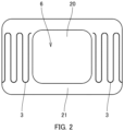
- FIG. 2 is a plan view of an accommodating recess 6 in a card body 2 that contains an IC chip module 4.
- FIG. 3 shows manufacturing steps for the smart card 1
- FIG. 4 is a plan view of the antenna connection terminal 5 of the IC chip module 4.
- the smart card 1 includes a card body 2 with an antenna coil 3 built in; and an IC chip module 4 provided with an antenna connection terminal 5 for conductive connection with the antenna coil 3, the IC chip module 4 being housed in an accommodating recess 6 in the card body 2, wherein the antenna coil 3 and the antenna connection terminal 5 are conductively connected via a conductive adhesive 9 in which conductive particles 8 are blended with binder resin 7, and the antenna connection terminal 5 has an opening 10 with a width larger than the average particle diameter of the conductive particles 8.
- the IC chip module 4 is bonded to the accommodating recess 6 of the card body 2 by thermocompression bonding via the conductive adhesive 9, so that the antenna coil 3 exposed to the accommodating recess 6 and the antenna connection terminal 5 provided on the IC chip module 4 are electrically connected via the conductive particles 8.
- the opening 10 having a width larger than the average particle diameter of the conductive particles 8 is formed in the antenna connection terminal 5, so that the flowability of the binder resin can be improved by thermal compression, and it is not necessary to apply high pressure. Therefore, it is possible to prevent deformation of the card body 2.
- the adhesive force can be improved by allowing the binder resin 7 to also flow into the opening 10 provided in the antenna connection terminal 5.
- the card body 2 is a laminate that includes an inlay 11 provided with the antenna coil 3, first and second core sheets 13a, 13b laminated appropriately on both sides of the inlay 11, and an overlay 12 that constitutes the front and back surfaces of the card body 2.
- the inlay 11, the first and second core sheets 13a, 13b, and the overlay 12 are made of resin material, for example.
- Resins that can be used to form the inlay 11, the first and second core sheets 13a, 13b, and the overlay 12 include, e.g., polyvinyl chloride (PVC), polyethylene terephthalate (PET), PET-G, PC (polycarbonate), PET-G, or recycled materials made from these, and biodegradable plastics such as Ocean Plastic, PLA (polylactic acid), among others.
- the card body 2 is formed by laminating and integrating the inlay 11, the core sheets 13, and the overlay 12, which constitute each layers, via adhesive or without adhesive by heating and pressing.
- thermoplastic or thermosetting materials can be used for the adhesive that bonds the layers of the inlay 11, the first and second core sheets 13a, 13b, and the overlay 12, but those having resistance to the cutting step for the card body 2 and heat resistance to the thermal compression pressure bonding step with the IC chip module 4 are suitable, and thermosetting adhesives are most suitable.
- the inlay 11 has the antenna coil 3 formed from a Cu wire and the like that wraps around the outer circumference multiple times. As shown in FIG. 2 , part of the antenna coil 3 is exposed to the outside from the accommodating recess 6 formed in the card body 2 and sandwiches the conductive particles 8 of the conductive adhesive 9 with the antenna connection terminal 5 of the IC chip module 4, thereby conductively connected to the antenna connection terminal 5 via the conductive particles 8.
- the inlay 11 holds the conductive particles 8
- at least the connection portion of the antenna coil 3 to be connected with the antenna connection terminal 5 is exposed by cutting.
- the cutting depth is set to a range not exceeding 50% of the antenna coil 3 diameter, preferably a range of 40% or more but less than 50% of the antenna coil 3 diameter, taking into account factors such as preventing the antenna coil 3 from falling off during the cutting process and ensuring sufficient contact area with the conductive particles 8.
- the trapping and contact area of the conductive particles 8 can be secured by using the conductive adhesive 9 with a predetermined particle area ratio with respect to the overlapping area Y between the antenna coil 3 and the antenna connection terminal 5.
- the overlapping area Y can be secured, it is not necessary to expose all of the antenna coil 3 connected to the antenna connection terminal 5, so that it is also possible to partially expose it.
- the level difference between the exposed and unexposed parts of the antenna coil 3 must be less than the particle diameter of the conductive particles 8. This prevents the risk of the antenna coil 3 falling off during the cutting process and reducing the overlapping area Y, and the risk of the fallen antenna coil 3 getting caught between another antenna coil 3 and the antenna connection terminal 5, preventing the conductive particles 8 from being sandwiched, among other risks.
- the card body 2 has an accommodating recess 6 for housing the IC chip module 4.
- the accommodating recess 6 is provided with a first recess 20 that accommodates the resin mold portion 35 of the IC chip module 4, and a second recess 21 that is provided on both sides of the first recess 20 and accommodates the terminal portion 36 on which the antenna connection terminal 5 of the IC chip module 4 is formed.
- the antenna coil 3, which is conductively connected to the antenna connection terminal 5, is exposed in the second recess 21.
- the first recess 20 has a depth D1 corresponding to the height of the resin mold portion 35 of the IC chip module 4, and the second recess 21 has a depth D2 corresponding to the thickness of the terminal portion 36 of the IC chip module 4 and the adhesive layer formed by the conductive adhesive 9.
- the depth D2 of the second recess 21 is shallower than the depth D1 of the first recess 20, and the first recess 20 and the second recess 21 are connected in a stair-like manner.
- the depth D1 and depth D2 both refer to the distance from the front surface of the card body 2 where the accommodating recess 6 is provided to the bottom surface of each recess.
- the accommodating recesses 6 can be formed by cutting using a milling machine that is numerically controlled (NC control) by a program.
- the IC chip module 4 has contact terminals 31 including, e.g., six or eight contact terminals on a front surface of the module substrate 30.
- the IC chip module 4 also has an IC chip 32 on the back surface opposite the front surface of the module substrate 30, which is used for both contact and non-contact applications, and the IC chip 32 is sealed by encapsulating resin 33, so that a resin mold portion 35 protrudes from the back surface of the module substrate 30.
- the resin mold portion 35 is embedded in the first recess 20 when the IC chip module 4 is housed in the accommodating recess 6.
- the terminal portion 36 with the antenna connection terminal 5 connected to a non-contact interface of the IC chip 32 via, e.g., a wire is provided on both sides of the resin mold portion 35.
- the terminal portion 36 is embedded in the second recess 21 when the IC chip module 4 is embedded in the accommodating recess 6.
- the antenna connection terminal 5 is formed into a predetermined shape by etching, e.g., copper foil and is appropriately nickel-plated or gold-plated, for example. As shown in FIG. 4 , the antenna connection terminal 5 of the present technology has an opening 10 with a width larger than the average particle diameter of the conductive particles 8 contained in the conductive adhesive 9.
- the opening 10 is formed as a slit 10a extending from the outer edge of the antenna connection terminal 5 inward, or as a hole 10b formed on the inner side of the antenna connection terminal 5. Since the opening 10 has a width larger than the average particle diameter of the conductive particles 8, the conductive particles 8 do not become clogged and the flowability of the binder resin 7 can be improved. Therefore, when connecting the IC chip module 4 via the conductive adhesive 9, the binder resin 7 and the conductive particles 8 can be filled into the second recess 21 without applying high pressure. This prevents deformation of the card body 2. In addition, the binder resin 7 flows into the opening 10, which allows the binder resin 7 to spread throughout the entire second recess 21, thereby improving the adhesive force.
- FIG. 5 shows a plan view of the pattern examples of the opening 10.
- FIGS. 5 (A) to (C) show pattern examples of openings formed by slits 10a having an open end on the outer edge of the rectangular antenna connection terminal 5
- FIGS. 5 (D) to (F) show pattern examples of openings formed by slits 10a and/or holes 10b inside the rectangular antenna connection terminal 5
- FIGS. 5 (G) to (H) show pattern examples of openings formed by slits 10a having an open end on the outer edge of an elliptical shape antenna connection terminal
- FIGS. 5 (I) to (J) show pattern examples of openings formed by slits 10a or holes 10b inside an elliptical shape antenna connection terminal.
- the longitudinal direction of the opening 10 is different from the wiring direction in which the antenna coil 3 extends. Since the opening 10 is a part that does not contribute to conductivity with the antenna coil 3 via the conductive particles 8, if the longitudinal direction of the opening 10 is the same as the wiring direction (extension direction) of the antenna coil 3, the opening 10 and the antenna coil 3 may overlap depending on the arrangement, which may reduce the number of trapped conductive particles 8 so that good conductivity may not be ensured.
- the pattern of the opening 10 is a symmetrical pattern in the plan view of the antenna connection terminal 5. This ensures that the heat and pressure applied when connecting to the IC chip module 4 is evenly distributed across the entire antenna connection terminal 5, allowing the binder resin 7 and conductive particles 8 to flow without any bias, and improving the probability of particle trapping of the conductive particles 8.
- the width of the opening 10 i.e., the width of the slit 10a or the diameter or minor axis of the hole 10b, is preferably 100 ⁇ m or more, more preferably 150 ⁇ m or more. By making the width of the opening 10 at least 100 ⁇ m, the flowability will not be impeded even if multiple conductive particles 8 pass through the opening 10, as long as the conductive particles 8 have an average particle diameter used in general conductive adhesives 9.
- the width of the opening 10 is preferably 300 ⁇ m or less, and more preferably 200 ⁇ m or less. If the width of the opening 10 exceeds 300 ⁇ m, the area of the antenna connection terminal 5 will decrease relatively, which may impair the conductive connection with the antenna coil 3.
- the conductive adhesive 9 is supplied onto the antenna coil 3 in the second recess 21 in the form of a conductive adhesive film or conductive adhesive paste.
- the ratio of the total area of the conductive particles 8 to the area of the conductive adhesive 9 supplied in this second recess 21 is defined as the particle area ratio X (%).
- the conductive adhesive 9 contains at least the binder resin 7 and the conductive particles 8, and may also contain other components as necessary.
- the conductive adhesive 9 is interposed between the IC chip module 4 and the antenna coil 3 exposed in the accommodating recess 6, and electrically connects the antenna connection terminal 5 and the antenna coil 3.
- the conductive adhesive 9 also adheres the IC chip module 4 to the accommodating recess 6.
- the conductive adhesive 9 may be in the form of a film or a paste, but for improved processability it is preferable to be in the form of a film as shown in FIG. 9 . In other words, it may be a conductive adhesive film.
- binder resin 7 there are no particular restrictions on the binder resin 7, and it can be selected appropriately according to the purpose, e.g., crystalline resin and amorphous resin. There are no particular restrictions on the crystalline resin and amorphous resin, and it can be selected appropriately according to the purpose, e.g., phenoxy resin, polyester resin, acryl resin, epoxy resin, urethane resin, and polyamide resin.
- the binder resin 7 contain only crystalline resin in consideration of stability at room temperature and ability to bond at low temperatures in a short time.
- binder resin 7 contained in the conductive adhesive 9 there are no particular restrictions on the amount of binder resin 7 contained in the conductive adhesive 9, and it can be selected appropriately according to the purpose.
- the material of the conductive particles 8 there are no particular restrictions on the material of the conductive particles 8, and it can be selected appropriately according to the purpose, and examples include copper, iron, nickel, gold, silver, aluminum, zinc, stainless steel, and magnetic metal particles such as hematite (Fe 2 O 3 ), and magnetite (Fe 3 O 4 ).
- the conductive particles 8 may be a particles with magnetic metals plated on resin cores such as acryl resin, acrylonitrile-styrene (AS) resin, benzoguanamine resin, divinylbenzene resin, styrene resin, and the like or an inorganic core particle such as silver-plated copper particle.
- the conductive particles 8 may also be coated with a metal plating film, such as Ag plating, Ni/Au plating, Ni/Pd plating, or Ni/Pd/Au plating. These conductive particles may be used individually or in combination.
- the conductive particles 8 may also be solder particles.
- solder particles there are no particular restrictions on whether the alloy is eutectic or non-eutectic, but it is preferable that the alloy contains two or more elements selected from the group consisting of Sn, Bi, Ag, In, Cu, Sb, Pb, and Zn.
- the average particle diameter of the conductive particles 8 there are no particular restrictions on the average particle diameter of the conductive particles 8, and it can be selected appropriately according to the purpose, but for example, it is preferably 20 ⁇ m to 50 ⁇ m, and more preferably, 30 ⁇ m to 40 ⁇ m, in order to correspond to the cutting level difference that occurs when the antenna coil 3 is cut.
- the thickness of the conductive adhesive 9 there are no particular restrictions on the thickness of the conductive adhesive 9, and it can be selected appropriately according to the purpose, e.g., 20 ⁇ m to 60 ⁇ m, and more preferably, 30 ⁇ m to 50 ⁇ m.
- the card body 2 is a laminate that has the inlay 11 with the antenna coil 3, the first and second core sheet 13a, 13b laminated appropriately on both sides of the inlay 11, and the overlay 12 that constitutes the front and back surfaces of the card body 2.
- Each layer that constitutes the card body 2 may be a single layer or laminated multiple layers.
- the following explanation uses an example of the card body 2 having a three-layer laminate consisting of the inlay 11 with the antenna coil formed therein and the first and second core sheets 13a, 13b laminated on the front and back surfaces of the inlay 11, and overlays 12 laminated on the front and back surfaces of the laminate.
- the card body 2 is formed by pasting the overlay 12 onto the front surface of the first core sheet 13a laminated to the front surface of the inlay 11 and the front surface of the second core sheet 13b laminated to the back surface of the inlay 11.
- the inlay 11 and the first and second core sheets 13a, 13b, and the first and second core sheets 13a, 13b and the overlay 12 are laminated via an adhesive layer not shown in the figure.
- the inlay 11 and the first and second core sheets 13a, 13b, and the first and second core sheets 13a, 13b and the overlay 12 may be laminated by being heated and pressed without using an adhesive.
- the first and second core sheets 13a, 13b are appropriately processed by printing, embossing, and the like.
- the antenna coil 3 made of a Cu wire and the like that wraps around the circumference of the substrate several times is embedded in the surface layer of a resin substrate, such as polyvinyl chloride (PVC).
- the first and second core sheets 13a, 13b are made of the same type of resin substrate as the inlay 11, for example polyvinyl chloride (PVC).
- the thickness of the inlay 11 can be, e.g., 340 to 380 ⁇ m.
- the thickness of the first and second core sheets 13a, 13b can be, e.g., 160 to 170 ⁇ m each.
- the thickness of the overlay 12 laminated to the first and second core sheets 13a, 13b can be, e.g., 60 to 80 ⁇ m each.
- the first recess 20 accommodating the resin mold portion 35 of the IC chip module 4 and the second recess 21 accommodating the terminal portion 36 of the IC chip module 4 are formed in the card body 2 by cutting with a NC-controlled milling machine or the like.
- the depth D1 of the first recess 20 is determined by taking into account the thickness of the resin mold portion 35 of the IC chip module 4, so that when the card body 2 is bent, the bottom surface of the first recess 20 does not come into contact with the resin mold portion 35 to push up it in the direction of peeling off from the accommodating recess 6, as well as by taking into account the need to ensure strength by leaving a certain amount (100 ⁇ m or more, preferably 150 ⁇ m or more) of the thickness of the second core sheet 13b and the overlay 12 remaining at the bottom of the first recess 20.
- the depth D2 of the second recess is set by taking into account the thickness of the terminal portion 36 of the IC chip module 4 and the thickness of the conductive adhesive 9 after adhesion, so that when the IC chip module 4 is fixed to the card body 2, the level difference D3 between the front surface of the IC chip module 4 and the front surface of the card body 2 is within the range of -100 to 50 ⁇ m.
- the depth D1 of the first recess 20 is 625 ⁇ m, assuming that the thickness of the resin mold portion 35 of the IC chip module 4 is 510 to 590 ⁇ m and the thickness of the second core sheet 13b and the overlay 12 remaining under the first recess 20 is 150 ⁇ m or more in order to maintain the strength of the card body 2.
- the depth D2 of the second recess 21 is 275 ⁇ m, for example, assuming that the thickness of the overlay 12 is 60 ⁇ m, the thickness of the terminal portion 36 of the IC chip module 4 is 235 ⁇ m (module substrate 30 thickness: 200 ⁇ m, antenna connection terminal 5 thickness: 35 ⁇ m), and the thickness of the conductive adhesive 9 under the antenna connection terminal 5 is 15 to 30 ⁇ m.
- the level difference D3 between the front surface of the IC chip module 4 and the front surface of the card body 2 is -25 ⁇ m.
- the total thickness of the second core sheet 13b and the overlay 12 under the first recess 20 is 185 ⁇ m.
- the IC chip module 4 is placed in the accommodating recess 6 via the conductive adhesive 9 in which the conductive particles 8 are blended with the binder resin 7.
- the conductive adhesive film is pasted to the second recess 21 or the IC chip module 4, and the IC chip module 4 is placed in the accommodating recess 6.
- FIG. 12 is a bottom view showing the IC chip module 4 with the conductive adhesive film pasted, with the portion corresponding to the resin mold portion 35 removed. It is also possible to paste the film without removing the portion, but in this case, the depth D1 of the first recess 20 is set so that is does not contact the bottom surface of the recess 20 even when the thickness of the conductive adhesive film is added to the thickness of the resin mold portion 35 of the IC chip module 4.
- the conductive adhesive paste is filled only in the exposed portion of the second recess 21 exposing the antenna coil 3.
- the IC chip module 4 is then heated and pressed at a predetermined temperature for a predetermined period of time, and the IC chip module 4 is fixed in the accommodating recess 6 while the antenna coil 3 and the antenna connection terminal 5 are conductively connected.
- the antenna coil 3 and the antenna connection terminal 5 are connected via the conductive particles 8 contained in the conductive adhesive 9 (see FIG. 3 (B) ).
- the opening 10 having a width larger than the average particle diameter of the conductive particles 8 is formed in the antenna connection terminal 5, so that the flowability of the binder resin 7 can be improved by thermal compression bonding, and it is not necessary to apply high pressure. Therefore, it is possible to prevent deformation of the card body 2.
- the adhesive force can also be improved by allowing the binder resin 7 to flow into the opening 10 provided in the antenna connection terminal 5.
- the adhesive strength of the IC chip module 4 is 50N or more for IC chip modules 4 with a surface area of up to 100 mm 2 , and 0.5 N/mm 2 for IC chip modules 4 with a surface area exceeding 100 mm 2 .
- an IC chip module with a slit in the antenna connection terminal and an IC chip module without a slit or other opening in the antenna connection terminal were prepared and respectively connected to the accommodating recess in the card body via a conductive adhesive film to fabricate smart cards. Then a bending test and an adhesive strength test were conducted on each smart card.
- An anisotropic conductive film (manufactured by DEXERIALS: EH1038-40) containing silver-plated copper particles with an average particle diameter of 38 ⁇ m was used as the conductive adhesive to connect the IC chip module to the card body.
- the anisotropic conductive film with the part overlapping the resin mold portion of the IC chip module removed was pasted to the entire surface of the IC chip module including the antenna connection terminal facing the second recess.
- This IC chip module was housed in the accommodating recess in the card body, and the smart card was prepared by thermocompression-bonding the IC chip module three times at 215°C-1.0s.
- the smart cards in the examples and comparative examples were subjected to cyclic bending force in the specified strength and direction. Then the Q value was measured using a resonance frequency checker MP300CL3 (manufactured by Micropross) for the smart cards after 4,000 cycles of bending. If the Q value decreased by 20% or more, the evaluation was "B (bad)", and if it did not decrease by 20% or more, the evaluation was "G (good)”.
- Example 2 a smart card was prepared by thermocompression-bonding the IC chip module three times at 215°C-2.5 bar-1.0s, i.e., with a pressing force of 2.5 bar. The other conditions were the same as in Example 1.
- Comparative Example 1 an IC chip module was used that did not have a slit formed in the antenna connection terminal.
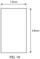
- the antenna connection terminal had a rectangular shape with a width of 1.5 mm and a length of 2.6 mm, as shown in FIG. 14 , and no slit was formed.
- a smart card was prepared by thermocompression-bonding the IC chip module three times at 215°C-2.5 bar-1.0s, i.e., with a pressing force of 2.5 bar.
- Comparative Example 2 a smart card was prepared by thermocompression-bonding the IC chip module three times at 215°C-1.5 bar-1.0s, i.e., with a pressing force of 1.5 bar. The other conditions were the same as Comparative Example 1.
- Comparative Example 1 where no slit was formed in the antenna connection terminal, even at a pressing force of 2.5 bar, the adhesive strength was lower than in Example 1, where the pressing force was lower.
- Comparative Example 2 where the pressing force was 1.5 bar, there was a greater decrease in the adhesive strength, and the bending test evaluation was B (bad).
Landscapes
- Engineering & Computer Science (AREA)
- Microelectronics & Electronic Packaging (AREA)
- Computer Hardware Design (AREA)
- Physics & Mathematics (AREA)
- General Physics & Mathematics (AREA)
- Theoretical Computer Science (AREA)
- Computer Networks & Wireless Communication (AREA)
- Manufacturing & Machinery (AREA)
- Credit Cards Or The Like (AREA)
Abstract
Description
- The present technology relates to a smart card equipped with an IC chip. This application claims priority based on
Japanese Patent Application No. 2022-125002, which was filed in Japan on August 4, 2022 - In recent years, smart cards, which contain an IC chip that can store information, have become widespread. Smart cards are classified into "contact type," "non-contact type," and "contact/non-contact combined type" according to the method of writing and reading data, and the contact/non-contact combined type is also called a dual interface card.
-
FIG. 15 shows a configuration example of a "contact/non-contact combined type" smart card. Thesmart card 100 shown inFIG. 15 includes acard body 101 and anIC chip module 102. Thecard body 101 is formed in a roughly rectangular plate shape, and has an inlay with anantenna coil 105 formed thereon, core sheets laminated to both sides of the inlay, and overlays provided on each surface of the core sheets. In addition, thecard body 101 has a chip accommodatingrecess 106 formed by cutting, in which theIC chip module 102 is housed. The chip accommodatingrecess 106 exposes twoends antenna coil 105 inside, thereby being conductive with the pair ofantenna connection terminals IC chip module 102. -
FIG. 16 is a cross-sectional view of theIC chip module 102 for both contact and non-contact applications. The contact/non-contactIC chip module 102 has acontact terminal 111 on the front surface of themodule substrate 110 and a contact/non-contact IC chip 112 on the back surface opposite the front surface of themodule substrate 110, and theIC chip 112 is sealed by encapsulatingresin 114. In theIC chip 112, a non-contact interface is connected to theantenna connection terminals wires 115, for example. Theantenna connection terminals module substrate 110, and when theIC chip module 102 is housed in the chip accommodatingrecess 106 of thecard body 101, it is conductively connected to the bothends antenna coil 105 via the conductive adhesive that fills the chip accommodatingrecess 106. - Melted metal (solder paste or silver paste) is used as the conductive adhesive that connects the both
ends antenna coil 105 to the antenna connection terminal 113, and hot melt adhesive is used in combination as a reinforcing component as appropriate. -
- Patent Document 1:
JP 2017-117468 A - Patent Document 2:
JP 5964187 B - The
antenna connection terminals IC chip module 102 are made up of a rectangular or other solid metal pattern, and while they have the advantage of being able to improve the connection area with the bothends antenna coil 105 due to their large connection area, the large amount of metal surface facing the conductive adhesive reduces the adhesive force. For this reason, there is a risk that theIC chip module 102 will peel away from the chip accommodatingrecess 106 when the smart card is bent. - Also, when embedding the
IC chip module 102 in the chip accommodatingrecess 106, the pressure required to flow the softened conductive adhesive becomes high. If this pressure is high, the deformation of the card becomes visually noticeable and undesirable from a quality standpoint. - Therefore, an object of the present technology is to provide a smart card that can improve the adhesive force of the IC chip module even under low pressure, and prevent the deformation of the card by increasing the flowability of the conductive adhesive.
- In order to solve the above-mentioned problem, a smart card according to the present technology includes: a card body with an antenna coil built in; and an IC chip module provided with an antenna connection terminal for conductive connection with the antenna coil, the IC chip module being housed in an accommodating recess in the card body, wherein the antenna coil and the antenna connection terminal are conductively connected via a conductive adhesive in which conductive particles are blended with binder resin, and the antenna connection terminal has an opening with a width larger than the average particle diameter of the conductive particles.
- In addition, a method for manufacturing a smart card according to the present technology includes: a step of preparing a card body with an antenna coil built in, and an IC chip module provided with an antenna connection terminal for conductive connection with the antenna coil, the IC chip module to be housed in an accommodating recess in the card body; a step of housing the IC chip module in the accommodating recess via a conductive adhesive in which conductive particles are blended with binder resin; and a step of heating and pressing the IC chip module to fix the IC chip module in the accommodating recess and conductively connect the antenna coil and the antenna connection terminal, wherein the antenna connection terminal has an opening with a width larger than the average particle diameter of the conductive particles.
- According to the present technology, the adhesive force of the IC chip module can be improved even under low pressure, and the flowability of the conductive adhesive can be increased to prevent deformation of the card.
-
-
FIG. 1 is a disassembled perspective view of an example of a smart card. -
FIG. 2 is a top view of an accommodating recess of the card body. -
FIG. 3 shows the manufacturing steps forsmart card 1, in which view (A) shows the IC chip module before housed in the accommodating recess and view (B) shows the IC chip module housed in the accommodating recess. -
FIG. 4 is a plan view of an example of an antenna connection terminal. -
FIG. 5 is a plan view of example patterns of openings provided in the antenna connection terminal. -
FIG. 6 is a plan view showing a configuration in which the longitudinal direction of the opening provided in the antenna connection terminal is different from the wiring direction in which the antenna coil extends. -
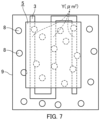
FIG. 7 is a plan view to explain overlapping area Y shared by the antenna connection terminal and the antenna coil and the particle area ratio X, which is the area ratio of the total area of the conductive particles within the area of the conductive adhesive. -
FIG. 8 is a graph showing the relationship between the overlapping area Y shared by the antenna connection terminal and the antenna coil and the particle area ratio X, which is the area ratio of the total area of the conductive particles within the area of the conductive adhesive. -
FIG. 9 is a cross-sectional view of the conductive adhesive formed in film form. -
FIG. 10 is a cross-sectional view of a card body, with overlays attached to the surface of the first and second core sheets, which are laminated to both sides of the inlay. -
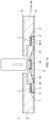
FIG. 11 is a cross-sectional view illustrating dimensional examples of the card body and the IC chip module. -
FIG. 12 is a bottom view of the IC chip module with the conductive adhesive film attached, with the part corresponding to the resin mold removed. -
FIG. 13 is a cross-sectional view illustrating a method of conducting an adhesive strength test on the smart card in an example. -
FIG. 14 is a plan view of the antenna connection terminal in a comparative example. -
FIG. 15 is a disassembled perspective view of a configuration example of the structure of a contact/non-contact combined type smart card. -
FIG. 16 is a cross-sectional view of the IC chip module for both contact and non-contact applications. - Embodiments of the smart card according to the present technology will now be more particularly described with reference to the accompanying drawings. It should be noted that the present technology is not limited to the embodiments described below and various modifications can be added to the embodiment without departing from the scope of the present technology. The features shown in the drawings are illustrated schematically and are not intended to be drawn to scale. Actual dimensions should be determined in consideration of the following description. Moreover, those skilled in the art will appreciate that dimensional relations and proportions may be different among the drawings in some parts.
- In this specification, the smart card is a card that incorporates an integrated circuit (IC) for recording and calculating information (data), and is also referred to as an "integrated circuit card" or "chip card". The smart card may be a dual interface card having two interfaces of a contact type and a non-contact type in one IC chip, or a hybrid card with both a contact type IC chip and a non-contact type IC chip. In addition, the smart card may be a fingerprint authentication card having fingerprint authentication elements or a card having a one-time password functions incorporating a battery element and a display element. These IC chips and elements are provided with antenna connection terminals and are electrically connected to the antenna coil functioning as an electrode on the card body side.
-
FIG. 1 is a schematic perspective view of an example of asmart card 1 according to the present technology, andFIG. 2 is a plan view of anaccommodating recess 6 in acard body 2 that contains anIC chip module 4.FIG. 3 shows manufacturing steps for thesmart card 1, andFIG. 4 is a plan view of theantenna connection terminal 5 of theIC chip module 4. - The
smart card 1 according to the present technology includes acard body 2 with anantenna coil 3 built in; and anIC chip module 4 provided with anantenna connection terminal 5 for conductive connection with theantenna coil 3, theIC chip module 4 being housed in anaccommodating recess 6 in thecard body 2, wherein theantenna coil 3 and theantenna connection terminal 5 are conductively connected via aconductive adhesive 9 in whichconductive particles 8 are blended withbinder resin 7, and theantenna connection terminal 5 has anopening 10 with a width larger than the average particle diameter of theconductive particles 8. - In the
smart card 1, theIC chip module 4 is bonded to theaccommodating recess 6 of thecard body 2 by thermocompression bonding via theconductive adhesive 9, so that theantenna coil 3 exposed to theaccommodating recess 6 and theantenna connection terminal 5 provided on theIC chip module 4 are electrically connected via theconductive particles 8. In thesmart card 1 according to the present technology, the opening 10 having a width larger than the average particle diameter of theconductive particles 8 is formed in theantenna connection terminal 5, so that the flowability of the binder resin can be improved by thermal compression, and it is not necessary to apply high pressure. Therefore, it is possible to prevent deformation of thecard body 2. In addition, the adhesive force can be improved by allowing thebinder resin 7 to also flow into theopening 10 provided in theantenna connection terminal 5. - The
card body 2 is a laminate that includes aninlay 11 provided with theantenna coil 3, first andsecond core sheets inlay 11, and anoverlay 12 that constitutes the front and back surfaces of thecard body 2. Theinlay 11, the first andsecond core sheets overlay 12 are made of resin material, for example. Resins that can be used to form theinlay 11, the first andsecond core sheets overlay 12 include, e.g., polyvinyl chloride (PVC), polyethylene terephthalate (PET), PET-G, PC (polycarbonate), PET-G, or recycled materials made from these, and biodegradable plastics such as Ocean Plastic, PLA (polylactic acid), among others. Thecard body 2 is formed by laminating and integrating theinlay 11, the core sheets 13, and theoverlay 12, which constitute each layers, via adhesive or without adhesive by heating and pressing. - Various materials such as thermoplastic or thermosetting materials can be used for the adhesive that bonds the layers of the
inlay 11, the first andsecond core sheets overlay 12, but those having resistance to the cutting step for thecard body 2 and heat resistance to the thermal compression pressure bonding step with theIC chip module 4 are suitable, and thermosetting adhesives are most suitable. - The
inlay 11 has theantenna coil 3 formed from a Cu wire and the like that wraps around the outer circumference multiple times. As shown inFIG. 2 , part of theantenna coil 3 is exposed to the outside from theaccommodating recess 6 formed in thecard body 2 and sandwiches theconductive particles 8 of theconductive adhesive 9 with theantenna connection terminal 5 of theIC chip module 4, thereby conductively connected to theantenna connection terminal 5 via theconductive particles 8. There are no particular restrictions on the pattern of theantenna coil 3 at the connection portion to be connected with theantenna connection terminal 5, but from the perspective of securing a large overlapping area with theantenna connection terminal 5, it is preferable to have a pattern with a zigzag shape, as shown inFIG. 2 . - In addition, because the
inlay 11 holds theconductive particles 8, at least the connection portion of theantenna coil 3 to be connected with theantenna connection terminal 5 is exposed by cutting. The cutting depth is set to a range not exceeding 50% of theantenna coil 3 diameter, preferably a range of 40% or more but less than 50% of theantenna coil 3 diameter, taking into account factors such as preventing theantenna coil 3 from falling off during the cutting process and ensuring sufficient contact area with theconductive particles 8. - Even if the cutting depth is less than 40% of the
antenna coil 3 diameter, the trapping and contact area of theconductive particles 8 can be secured by using theconductive adhesive 9 with a predetermined particle area ratio with respect to the overlapping area Y between theantenna coil 3 and theantenna connection terminal 5. - Also, if the overlapping area Y can be secured, it is not necessary to expose all of the
antenna coil 3 connected to theantenna connection terminal 5, so that it is also possible to partially expose it. However, in that case, the level difference between the exposed and unexposed parts of theantenna coil 3 must be less than the particle diameter of theconductive particles 8. This prevents the risk of theantenna coil 3 falling off during the cutting process and reducing the overlapping area Y, and the risk of the fallenantenna coil 3 getting caught between anotherantenna coil 3 and theantenna connection terminal 5, preventing theconductive particles 8 from being sandwiched, among other risks. - The
card body 2 has anaccommodating recess 6 for housing theIC chip module 4. Theaccommodating recess 6 is provided with afirst recess 20 that accommodates theresin mold portion 35 of theIC chip module 4, and asecond recess 21 that is provided on both sides of thefirst recess 20 and accommodates theterminal portion 36 on which theantenna connection terminal 5 of theIC chip module 4 is formed. Theantenna coil 3, which is conductively connected to theantenna connection terminal 5, is exposed in thesecond recess 21. - As shown in
FIG. 3 (A) , thefirst recess 20 has a depth D1 corresponding to the height of theresin mold portion 35 of theIC chip module 4, and thesecond recess 21 has a depth D2 corresponding to the thickness of theterminal portion 36 of theIC chip module 4 and the adhesive layer formed by theconductive adhesive 9. The depth D2 of thesecond recess 21 is shallower than the depth D1 of thefirst recess 20, and thefirst recess 20 and thesecond recess 21 are connected in a stair-like manner. - The depth D1 and depth D2 both refer to the distance from the front surface of the
card body 2 where theaccommodating recess 6 is provided to the bottom surface of each recess. For example, theaccommodating recesses 6 can be formed by cutting using a milling machine that is numerically controlled (NC control) by a program. - The
IC chip module 4 hascontact terminals 31 including, e.g., six or eight contact terminals on a front surface of themodule substrate 30. TheIC chip module 4 also has anIC chip 32 on the back surface opposite the front surface of themodule substrate 30, which is used for both contact and non-contact applications, and theIC chip 32 is sealed by encapsulatingresin 33, so that aresin mold portion 35 protrudes from the back surface of themodule substrate 30. Theresin mold portion 35 is embedded in thefirst recess 20 when theIC chip module 4 is housed in theaccommodating recess 6. - The
terminal portion 36 with theantenna connection terminal 5 connected to a non-contact interface of theIC chip 32 via, e.g., a wire is provided on both sides of theresin mold portion 35. Theterminal portion 36 is embedded in thesecond recess 21 when theIC chip module 4 is embedded in theaccommodating recess 6. - The
antenna connection terminal 5 is formed into a predetermined shape by etching, e.g., copper foil and is appropriately nickel-plated or gold-plated, for example. As shown inFIG. 4 , theantenna connection terminal 5 of the present technology has anopening 10 with a width larger than the average particle diameter of theconductive particles 8 contained in theconductive adhesive 9. - The
opening 10 is formed as aslit 10a extending from the outer edge of theantenna connection terminal 5 inward, or as ahole 10b formed on the inner side of theantenna connection terminal 5. Since theopening 10 has a width larger than the average particle diameter of theconductive particles 8, theconductive particles 8 do not become clogged and the flowability of thebinder resin 7 can be improved. Therefore, when connecting theIC chip module 4 via theconductive adhesive 9, thebinder resin 7 and theconductive particles 8 can be filled into thesecond recess 21 without applying high pressure. This prevents deformation of thecard body 2. In addition, thebinder resin 7 flows into theopening 10, which allows thebinder resin 7 to spread throughout the entiresecond recess 21, thereby improving the adhesive force. -
FIG. 5 shows a plan view of the pattern examples of theopening 10.FIGS. 5 (A) to (C) show pattern examples of openings formed byslits 10a having an open end on the outer edge of the rectangularantenna connection terminal 5,FIGS. 5 (D) to (F) show pattern examples of openings formed byslits 10a and/orholes 10b inside the rectangularantenna connection terminal 5,FIGS. 5 (G) to (H) show pattern examples of openings formed byslits 10a having an open end on the outer edge of an elliptical shape antenna connection terminal, andFIGS. 5 (I) to (J) show pattern examples of openings formed byslits 10a or holes 10b inside an elliptical shape antenna connection terminal. - As shown in
FIG. 6 , when theopening 10 is formed as theslits 10a or theholes 10b having a long axis such as a rectangle or an ellipse, it is preferable that the longitudinal direction of theopening 10 is different from the wiring direction in which theantenna coil 3 extends. Since theopening 10 is a part that does not contribute to conductivity with theantenna coil 3 via theconductive particles 8, if the longitudinal direction of theopening 10 is the same as the wiring direction (extension direction) of theantenna coil 3, theopening 10 and theantenna coil 3 may overlap depending on the arrangement, which may reduce the number of trappedconductive particles 8 so that good conductivity may not be ensured. By making the longitudinal direction of theopening 10 different from the wiring direction of theantenna coil 3, even if theantenna coil 3 overlaps with theopening 10, it will only be a partial overlap, and the overlapping area with theantenna connection terminal 5 can be secured. - In addition, it is preferable that the pattern of the
opening 10 is a symmetrical pattern in the plan view of theantenna connection terminal 5. This ensures that the heat and pressure applied when connecting to theIC chip module 4 is evenly distributed across the entireantenna connection terminal 5, allowing thebinder resin 7 andconductive particles 8 to flow without any bias, and improving the probability of particle trapping of theconductive particles 8. - The width of the
opening 10, i.e., the width of theslit 10a or the diameter or minor axis of thehole 10b, is preferably 100 µm or more, more preferably 150 µm or more. By making the width of theopening 10 at least 100 µm, the flowability will not be impeded even if multipleconductive particles 8 pass through theopening 10, as long as theconductive particles 8 have an average particle diameter used in generalconductive adhesives 9. In addition, the width of theopening 10 is preferably 300 µm or less, and more preferably 200 µm or less. If the width of theopening 10 exceeds 300 µm, the area of theantenna connection terminal 5 will decrease relatively, which may impair the conductive connection with theantenna coil 3. - As shown in
FIGS. 7 and8 , it is preferable that the overlapping area Y shared by theantenna connection terminal 5 and theantenna coil 3, and the particle area ratio X, which is the area ratio of the total area of theconductive particles 8 within the area of theconductive adhesive 9, satisfy the following relationship:

- In the case of an overlapping area Y with a value of 580,000 µm2 or more that deviates from the straight line in
FIG. 8 , the relationship will be satisfied even if the particle area is zero in the calculation, but of course this is not the case, and it is preferable to select theconductive adhesive 9 with a particle area ratio of at least 3.0%. - As described later, the
conductive adhesive 9 is supplied onto theantenna coil 3 in thesecond recess 21 in the form of a conductive adhesive film or conductive adhesive paste. The ratio of the total area of theconductive particles 8 to the area of theconductive adhesive 9 supplied in thissecond recess 21 is defined as the particle area ratio X (%). By setting the overlapping area Y (µm2) between theantenna connection terminal 5 and theantenna coil 3 to have the above relationship, even when taking into account the flow ofconductive particles 8 when connecting theIC chip module 4, the number of trappedconductive particles 8 by theantenna connection terminal 5 and theantenna coil 3 can be made to be 5 or more with a probability of Ave-3σ. - The
conductive adhesive 9 contains at least thebinder resin 7 and theconductive particles 8, and may also contain other components as necessary. Theconductive adhesive 9 is interposed between theIC chip module 4 and theantenna coil 3 exposed in theaccommodating recess 6, and electrically connects theantenna connection terminal 5 and theantenna coil 3. Theconductive adhesive 9 also adheres theIC chip module 4 to theaccommodating recess 6. - The
conductive adhesive 9 may be in the form of a film or a paste, but for improved processability it is preferable to be in the form of a film as shown inFIG. 9 . In other words, it may be a conductive adhesive film. - There are no particular restrictions on the
binder resin 7, and it can be selected appropriately according to the purpose, e.g., crystalline resin and amorphous resin. There are no particular restrictions on the crystalline resin and amorphous resin, and it can be selected appropriately according to the purpose, e.g., phenoxy resin, polyester resin, acryl resin, epoxy resin, urethane resin, and polyamide resin. - It is preferable that the
binder resin 7 contain only crystalline resin in consideration of stability at room temperature and ability to bond at low temperatures in a short time. - There are no particular restrictions on the amount of
binder resin 7 contained in theconductive adhesive 9, and it can be selected appropriately according to the purpose. - There are no particular restrictions on the material of the
conductive particles 8, and it can be selected appropriately according to the purpose, and examples include copper, iron, nickel, gold, silver, aluminum, zinc, stainless steel, and magnetic metal particles such as hematite (Fe2O3), and magnetite (Fe3O4). In addition, theconductive particles 8 may be a particles with magnetic metals plated on resin cores such as acryl resin, acrylonitrile-styrene (AS) resin, benzoguanamine resin, divinylbenzene resin, styrene resin, and the like or an inorganic core particle such as silver-plated copper particle. Theconductive particles 8 may also be coated with a metal plating film, such as Ag plating, Ni/Au plating, Ni/Pd plating, or Ni/Pd/Au plating. These conductive particles may be used individually or in combination. - The
conductive particles 8 may also be solder particles. In the case of solder particles, there are no particular restrictions on whether the alloy is eutectic or non-eutectic, but it is preferable that the alloy contains two or more elements selected from the group consisting of Sn, Bi, Ag, In, Cu, Sb, Pb, and Zn. - There are no particular restrictions on the average particle diameter of the
conductive particles 8, and it can be selected appropriately according to the purpose, but for example, it is preferably 20 µm to 50 µm, and more preferably, 30 µm to 40 µm, in order to correspond to the cutting level difference that occurs when theantenna coil 3 is cut. There are no particular restrictions on the content ofconductive particles 8 in theconductive adhesive 9, and it can be selected appropriately according to the purpose, e.g., 3.0 wt% to 80 wt%, and more preferably 5.0 wt% to 65 wt%. Furthermore, there are no particular restrictions on the thickness of theconductive adhesive 9, and it can be selected appropriately according to the purpose, e.g., 20 µm to 60 µm, and more preferably, 30 µm to 50 µm. - Next, a smart card manufacturing process will be explained. The smart card manufacturing process includes a step of preparing a
card body 2 with anantenna coil 3 built in and anIC chip module 4 provided with anantenna connection terminal 5 for conductive connection with theantenna coil 3, theIC chip module 4 to be housed in anaccommodating recess 6 in thecard body 2; a step of housing theIC chip module 4 in theaccommodating recess 6 via aconductive adhesive 9 in whichconductive particles 8 are blended withbinder resin 7; and a step of heating and pressing theIC chip module 4 to fix theIC chip module 4 in theaccommodating recess 6 and conductively connect theantenna coil 3 and theantenna connection terminal 5. - As described above, the
card body 2 is a laminate that has theinlay 11 with theantenna coil 3, the first andsecond core sheet inlay 11, and theoverlay 12 that constitutes the front and back surfaces of thecard body 2. Each layer that constitutes thecard body 2 may be a single layer or laminated multiple layers. The following explanation uses an example of thecard body 2 having a three-layer laminate consisting of theinlay 11 with the antenna coil formed therein and the first andsecond core sheets inlay 11, and overlays 12 laminated on the front and back surfaces of the laminate. - As shown in
FIG. 10 , thecard body 2 is formed by pasting theoverlay 12 onto the front surface of thefirst core sheet 13a laminated to the front surface of theinlay 11 and the front surface of thesecond core sheet 13b laminated to the back surface of theinlay 11. Theinlay 11 and the first andsecond core sheets second core sheets overlay 12 are laminated via an adhesive layer not shown in the figure. Alternatively, theinlay 11 and the first andsecond core sheets second core sheets overlay 12 may be laminated by being heated and pressed without using an adhesive. Before being laminated with theoverlay 12, the first andsecond core sheets - In the
inlay 11, theantenna coil 3 made of a Cu wire and the like that wraps around the circumference of the substrate several times is embedded in the surface layer of a resin substrate, such as polyvinyl chloride (PVC). The first andsecond core sheets inlay 11, for example polyvinyl chloride (PVC). - There is no particular restrictions on the thickness of the
inlay 11, which can be, e.g., 340 to 380 µm. There are also no particular restrictions on the thickness of the first andsecond core sheets overlay 12 laminated to the first andsecond core sheets - As shown in
FIG. 11 , thefirst recess 20 accommodating theresin mold portion 35 of theIC chip module 4 and thesecond recess 21 accommodating theterminal portion 36 of theIC chip module 4 are formed in thecard body 2 by cutting with a NC-controlled milling machine or the like. - The depth D1 of the
first recess 20 is determined by taking into account the thickness of theresin mold portion 35 of theIC chip module 4, so that when thecard body 2 is bent, the bottom surface of thefirst recess 20 does not come into contact with theresin mold portion 35 to push up it in the direction of peeling off from theaccommodating recess 6, as well as by taking into account the need to ensure strength by leaving a certain amount (100 µm or more, preferably 150 µm or more) of the thickness of thesecond core sheet 13b and theoverlay 12 remaining at the bottom of thefirst recess 20. - The depth D2 of the second recess is set by taking into account the thickness of the
terminal portion 36 of theIC chip module 4 and the thickness of theconductive adhesive 9 after adhesion, so that when theIC chip module 4 is fixed to thecard body 2, the level difference D3 between the front surface of theIC chip module 4 and the front surface of thecard body 2 is within the range of -100 to 50 µm. - In the example shown in
FIG. 11 , the depth D1 of thefirst recess 20 is 625 µm, assuming that the thickness of theresin mold portion 35 of theIC chip module 4 is 510 to 590 µm and the thickness of thesecond core sheet 13b and theoverlay 12 remaining under thefirst recess 20 is 150 µm or more in order to maintain the strength of thecard body 2. In addition, the depth D2 of thesecond recess 21 is 275 µm, for example, assuming that the thickness of theoverlay 12 is 60 µm, the thickness of theterminal portion 36 of theIC chip module 4 is 235 µm (module substrate 30 thickness: 200 µm,antenna connection terminal 5 thickness: 35 µm), and the thickness of theconductive adhesive 9 under theantenna connection terminal 5 is 15 to 30 µm. The level difference D3 between the front surface of theIC chip module 4 and the front surface of thecard body 2 is -25µm. In addition, the total thickness of thesecond core sheet 13b and theoverlay 12 under thefirst recess 20 is 185 µm. - Next, as shown in
FIG. 3 (A) , theIC chip module 4 is placed in theaccommodating recess 6 via theconductive adhesive 9 in which theconductive particles 8 are blended with thebinder resin 7. When using a conductive adhesive film as theconductive adhesive 9, the conductive adhesive film is pasted to thesecond recess 21 or theIC chip module 4, and theIC chip module 4 is placed in theaccommodating recess 6. - When the conductive adhesive film is pasted to the
IC chip module 4, the conductive adhesive film is not required for theresin mold portion 35, so the portion corresponding to theresin mold portion 35 can be removed before pasting.FIG. 12 is a bottom view showing theIC chip module 4 with the conductive adhesive film pasted, with the portion corresponding to theresin mold portion 35 removed. It is also possible to paste the film without removing the portion, but in this case, the depth D1 of thefirst recess 20 is set so that is does not contact the bottom surface of therecess 20 even when the thickness of the conductive adhesive film is added to the thickness of theresin mold portion 35 of theIC chip module 4. - When using conductive adhesive paste as the
conductive adhesive 9, the conductive adhesive paste is filled only in the exposed portion of thesecond recess 21 exposing theantenna coil 3. In addition, an adhesive film containing no conductive particles, from which the portion corresponding to the portion filled with conductive adhesive paste and theresin mold portion 35 is removed, is pasted to theIC chip module 4, and then theIC chip module 4 is housed in theaccommodating recess 6. - The
IC chip module 4 is then heated and pressed at a predetermined temperature for a predetermined period of time, and theIC chip module 4 is fixed in theaccommodating recess 6 while theantenna coil 3 and theantenna connection terminal 5 are conductively connected. Theantenna coil 3 and theantenna connection terminal 5 are connected via theconductive particles 8 contained in the conductive adhesive 9 (seeFIG. 3 (B) ). - In the
smart card 1 according to the present technology, theopening 10 having a width larger than the average particle diameter of theconductive particles 8 is formed in theantenna connection terminal 5, so that the flowability of thebinder resin 7 can be improved by thermal compression bonding, and it is not necessary to apply high pressure. Therefore, it is possible to prevent deformation of thecard body 2. The adhesive force can also be improved by allowing thebinder resin 7 to flow into theopening 10 provided in theantenna connection terminal 5. - In such a
smart card 1, the adhesive strength of theIC chip module 4 is 50N or more forIC chip modules 4 with a surface area of up to 100 mm2, and 0.5 N/mm2 forIC chip modules 4 with a surface area exceeding 100 mm2. - In addition, by improving the flowability of the
binder resin 7, it is possible to sandwich theconductive particles 8 with a uniform thickness in the plane of theantenna coil 3 and theantenna connection terminal 5, thereby improving the particle trapping rate. - Next, examples of the present technology will be explained. In these examples, an IC chip module with a slit in the antenna connection terminal and an IC chip module without a slit or other opening in the antenna connection terminal were prepared and respectively connected to the accommodating recess in the card body via a conductive adhesive film to fabricate smart cards. Then a bending test and an adhesive strength test were conducted on each smart card.
- An anisotropic conductive film (manufactured by DEXERIALS: EH1038-40) containing silver-plated copper particles with an average particle diameter of 38 µm was used as the conductive adhesive to connect the IC chip module to the card body. The anisotropic conductive film with the part overlapping the resin mold portion of the IC chip module removed was pasted to the entire surface of the IC chip module including the antenna connection terminal facing the second recess. This IC chip module was housed in the accommodating recess in the card body, and the smart card was prepared by thermocompression-bonding the IC chip module three times at 215°C-1.0s.
- In accordance with ISO 10373-1 5.8, the smart cards in the examples and comparative examples were subjected to cyclic bending force in the specified strength and direction. Then the Q value was measured using a resonance frequency checker MP300CL3 (manufactured by Micropross) for the smart cards after 4,000 cycles of bending. If the Q value decreased by 20% or more, the evaluation was "B (bad)", and if it did not decrease by 20% or more, the evaluation was "G (good)".
- A hole was made in the back surface of the smart card in the examples and comparative examples, and the adhesive strength was determined as the peak intensity when the back surface was peeled off at 30 mm/min using a 5 mm diameter metal rod (see
FIG. 13 ). - In Example 1, an IC chip module with a slit formed in the antenna connection terminal was used. As shown in
FIG. 4 , the antenna connection terminal had a rectangular shape with a width of 1.5 mm and a length of 2.6 mm, and four slits with a width of 0.15 mm and a length of 0.55 mm were formed in a symmetrical pattern at intervals of 0.4 mm in the longitudinal direction on both the left and right sides. A smart card was prepared by thermocompression-bonding the IC chip module three times at 215°C-1.5 bar-1.0s, i.e., with a pressing force of 1.5 bar. - In Example 2, a smart card was prepared by thermocompression-bonding the IC chip module three times at 215°C-2.5 bar-1.0s, i.e., with a pressing force of 2.5 bar. The other conditions were the same as in Example 1.
- In Comparative Example 1, an IC chip module was used that did not have a slit formed in the antenna connection terminal. The antenna connection terminal had a rectangular shape with a width of 1.5 mm and a length of 2.6 mm, as shown in
FIG. 14 , and no slit was formed. In addition, a smart card was prepared by thermocompression-bonding the IC chip module three times at 215°C-2.5 bar-1.0s, i.e., with a pressing force of 2.5 bar. - In Comparative Example 2, a smart card was prepared by thermocompression-bonding the IC chip module three times at 215°C-1.5 bar-1.0s, i.e., with a pressing force of 1.5 bar. The other conditions were the same as Comparative Example 1.
Table 1 EX. 1 EX. 2 Comp. 1 Comp. 2 antenna connection terminal (2.6x1.5mm) with slit ✔ ✔ without slit ✔ ✔ pressure 2.5bar ✔ ✔ pressure1.5bar ✔ ✔ evaluation of binding test G G G B adhesive strength(N) 115 120 110 105 - As shown in Table 1, in Example 1, in which the slits were formed in the antenna connection terminal, good adhesive strength was obtained even under low pressure of 1.5 bar. In Example 2, where the pressing force was set at 2.5 bar, there was a further improvement in adhesive strength. In addition, in all of the examples, the results of the bending test were "G (good)". This shows that by forming slits in the antenna connection terminal, the flowability of the conductive adhesive is improved, and high adhesive strength can be achieved even under low pressure.
- On the other hand, in Comparative Example 1, where no slit was formed in the antenna connection terminal, even at a pressing force of 2.5 bar, the adhesive strength was lower than in Example 1, where the pressing force was lower. In addition, in the Comparative Example 2, where the pressing force was 1.5 bar, there was a greater decrease in the adhesive strength, and the bending test evaluation was B (bad).
- 1 smart card, 2 card body, 3 antenna coil, 4 IC chip module, 5 antenna connection terminal, 6 accommodating recess, 7 binder resin, 8 conductive particles, 9 conductive adhesive, 10 opening, 10a slit, 10b hole, 11 inlay, 12 overlay, 13a first core sheet, 13b second core sheet, 20 first recess, 21 second recess, 30 module substrate, 31 contact terminal, 32 IC chip, 33 encapsulating resin, 35 resin mold portion, 36 terminal portion
Claims (9)
- A smart card, comprising:a card body with an antenna coil built in; andan IC chip module provided with an antenna connection terminal for conductive connection with the antenna coil, the IC chip module being housed in an accommodating recess in the card body, whereinthe antenna coil and the antenna connection terminal are conductively connected via a conductive adhesive in which conductive particles are blended with binder resin, andthe antenna connection terminal has an opening with a width larger than the average particle diameter of the conductive particles.
- The smart card according to claim 1, wherein the opening is a slit and/or a hole.
- The smart card according to claim 1 or 2, wherein the longitudinal direction of the opening is different from the wiring direction of the antenna coil.
- The smart card according to claim 1 or 2, wherein the pattern of the opening is a symmetrical pattern in plan view of the antenna connection terminal.
- The smart card according to claim 1 or 2, wherein the width of the opening is 100 µm or more and 300 µm or less.
- The smart card according to claim 1 or 2, wherein the overlapping area Y shared by the antenna connection terminal and the antenna coil, and the particle area ratio X, which is the area ratio of the total area of the conductive particles within the area of the conductive adhesive, satisfy the following relationship:


- The smart card according to claim 6 that also satisfies the following condition:

- A method for manufacturing a smart card, comprising:a step of preparing a card body with an antenna coil built in, and an IC chip module provided with an antenna connection terminal for conductive connection with the antenna coil, the IC chip module to be housed in an accommodating recess in the card body;a step of housing the IC chip module in the accommodating recess via a conductive adhesive in which conductive particles are blended with binder resin; anda step of heating and pressing the IC chip module to fix the IC chip module in the accommodating recess and conductively connect the antenna coil and the antenna connection terminal, whereinthe antenna connection terminal has an opening with a width larger than the average particle diameter of the conductive particles.
- A method for manufacturing a smart card according to claim 8, wherein the conductive adhesive film is laminated to the IC chip module, and then the IC chip module is housed in the accommodating recess.
Applications Claiming Priority (2)
| Application Number | Priority Date | Filing Date | Title |
|---|---|---|---|
| JP2022125002A JP2024021861A (en) | 2022-08-04 | 2022-08-04 | smart card |
| PCT/JP2023/024231 WO2024029250A1 (en) | 2022-08-04 | 2023-06-29 | Smart card |
Publications (2)
| Publication Number | Publication Date |
|---|---|
| EP4567666A1 true EP4567666A1 (en) | 2025-06-11 |
| EP4567666A4 EP4567666A4 (en) | 2026-07-29 |
Family
ID=89849110
Family Applications (1)
| Application Number | Title | Priority Date | Filing Date |
|---|---|---|---|
| EP23849809.1A Pending EP4567666A4 (en) | 2022-08-04 | 2023-06-29 | CHIP CARD |
Country Status (5)
| Country | Link |
|---|---|
| US (1) | US12670355B2 (en) |
| EP (1) | EP4567666A4 (en) |
| JP (1) | JP2024021861A (en) |
| CN (1) | CN119631081A (en) |
| WO (1) | WO2024029250A1 (en) |
Families Citing this family (2)
| Publication number | Priority date | Publication date | Assignee | Title |
|---|---|---|---|---|
| JP7673156B1 (en) | 2023-11-02 | 2025-05-08 | 株式会社東芝 | Inlay sheet, portable electronic device, and method for manufacturing inlay sheet |
| JP2026022169A (en) * | 2024-07-30 | 2026-02-12 | デクセリアルズ株式会社 | Hot melt adhesive sheet containing conductive particles, method for manufacturing smart card, and smart card |
Family Cites Families (15)
| Publication number | Priority date | Publication date | Assignee | Title |
|---|---|---|---|---|
| JPH08291833A (en) * | 1995-04-20 | 1996-11-05 | Tokico Ltd | Disc brake |
| JP3491595B2 (en) * | 2000-02-25 | 2004-01-26 | ソニーケミカル株式会社 | Anisotropic conductive adhesive film |
| JP2003168097A (en) * | 2001-11-29 | 2003-06-13 | Toppan Forms Co Ltd | Conductive connection |
| JP2004013733A (en) * | 2002-06-10 | 2004-01-15 | Matsushita Electric Ind Co Ltd | Non-contact data carrier and method of manufacturing the same |
| JP4090950B2 (en) * | 2003-06-26 | 2008-05-28 | 大日本印刷株式会社 | IC module for compound IC card |
| JP2005070915A (en) * | 2003-08-20 | 2005-03-17 | Dainippon Printing Co Ltd | Compound IC card and method of manufacturing compound IC card |
| KR100723491B1 (en) | 2005-07-14 | 2007-05-30 | 삼성전자주식회사 | Universal Printed Circuit Boards and Smart Cards Using the Same |
| JP2009031956A (en) * | 2007-07-26 | 2009-02-12 | Dainippon Printing Co Ltd | Contact / non-contact common type IC card and method of manufacturing contact / non-contact common type IC card |
| JP5964187B2 (en) | 2012-09-18 | 2016-08-03 | デクセリアルズ株式会社 | Anisotropic conductive film, connection method, and joined body |
| JP2015228234A (en) * | 2015-07-17 | 2015-12-17 | 株式会社トッパンTdkレーベル | Manufacturing method of non-contact communication medium, and connection method of antenna and circuit device |
| JP7005138B2 (en) * | 2015-12-22 | 2022-01-21 | デクセリアルズ株式会社 | IC card |
| KR102857758B1 (en) * | 2020-06-05 | 2025-09-09 | 데쿠세리아루즈 가부시키가이샤 | Method for manufacturing a smart card, a smart card, and a hot melt adhesive sheet containing conductive particles |
| JP6966659B1 (en) * | 2020-06-05 | 2021-11-17 | デクセリアルズ株式会社 | Smart card manufacturing method, smart card, and hot melt adhesive sheet containing conductive particles |
| JP7513430B2 (en) | 2020-06-05 | 2024-07-09 | デクセリアルズ株式会社 | Method for manufacturing joined body, joined body, and conductive particle-containing hot melt adhesive sheet |
| JP2022125002A (en) | 2021-02-16 | 2022-08-26 | 東京応化工業株式会社 | Method for producing semiconductor chip and protective film forming agent |
-
2022
- 2022-08-04 JP JP2022125002A patent/JP2024021861A/en active Pending
-
2023
- 2023-06-29 WO PCT/JP2023/024231 patent/WO2024029250A1/en not_active Ceased
- 2023-06-29 CN CN202380055627.4A patent/CN119631081A/en active Pending
- 2023-06-29 EP EP23849809.1A patent/EP4567666A4/en active Pending
- 2023-06-29 US US19/100,125 patent/US12670355B2/en active Active
Also Published As
| Publication number | Publication date |
|---|---|
| WO2024029250A1 (en) | 2024-02-08 |
| EP4567666A4 (en) | 2026-07-29 |
| JP2024021861A (en) | 2024-02-16 |
| US12670355B2 (en) | 2026-06-30 |
| US20260044703A1 (en) | 2026-02-12 |
| CN119631081A (en) | 2025-03-14 |
Similar Documents
| Publication | Publication Date | Title |
|---|---|---|
| US8689428B2 (en) | Method and system for manufacturing an electronic interface apparatus | |
| US4719140A (en) | Electronic memory card | |
| US6435415B1 (en) | Contactless electronic memory card | |
| CN108885709B (en) | Method for manufacturing a chip card and a chip card antenna support | |
| US20260044703A1 (en) | Smart card | |
| EP3151167B1 (en) | Dual-interface ic card module | |
| JP2000182017A (en) | Contact type non-contact type shared IC card and method of manufacturing the same | |
| JP2004310619A (en) | Method for manufacturing ic card | |
| TWI284842B (en) | Communication medium capable of carrying out contactless communication and method of producing the same | |
| TWI900732B (en) | Method for manufacturing smart card modules and strip of flexible material supporting such modules | |
| JPH0216233B2 (en) | ||
| JP2005070915A (en) | Compound IC card and method of manufacturing compound IC card | |
| AU4043699A (en) | Method for producing an integrated circuit card and card produced according to said method | |
| JP4952266B2 (en) | Dual interface IC card and its manufacturing method, contact / non-contact IC module | |
| KR102835167B1 (en) | Metal combi card and method for producing thereof | |
| US10804226B2 (en) | Method for manufacturing chip cards and chip card obtained by said method | |
| JP3769332B2 (en) | IC card manufacturing method | |
| JPH11115355A (en) | Composite IC card and method of manufacturing the same | |
| JP2021117791A (en) | Contact/non-contact common use ic card and method for manufacturing contact/non-contact common use ic card | |
| JP2000311225A (en) | Non-contact IC card | |
| EP1804202A1 (en) | Tape carrier and module for contact type IC card and method for manufacturing the tape carrier | |
| JP7806590B2 (en) | Dual interface IC card and its manufacturing method | |
| JP2003248808A (en) | IC module for IC card, contact type non-contact type shared IC card, non-contact type IC card | |
| JP7838304B2 (en) | Dual-interface IC card and method for manufacturing the same | |
| JP2026071875A (en) | IC card |
Legal Events
| Date | Code | Title | Description |
|---|---|---|---|
| STAA | Information on the status of an ep patent application or granted ep patent |
Free format text: STATUS: THE INTERNATIONAL PUBLICATION HAS BEEN MADE |
|
| PUAI | Public reference made under article 153(3) epc to a published international application that has entered the european phase |
Free format text: ORIGINAL CODE: 0009012 |
|
| STAA | Information on the status of an ep patent application or granted ep patent |
Free format text: STATUS: REQUEST FOR EXAMINATION WAS MADE |
|
| 17P | Request for examination filed |
Effective date: 20250206 |
|
| AK | Designated contracting states |
Kind code of ref document: A1 Designated state(s): AL AT BE BG CH CY CZ DE DK EE ES FI FR GB GR HR HU IE IS IT LI LT LU LV MC ME MK MT NL NO PL PT RO RS SE SI SK SM TR |
|
| DAV | Request for validation of the european patent (deleted) | ||
| DAX | Request for extension of the european patent (deleted) | ||
| A4 | Supplementary search report drawn up and despatched |
Effective date: 20260624 |
|
| RIC1 | Information provided on ipc code assigned before grant |
Ipc: G06K 19/077 20060101AFI20260623BHEP Ipc: B42D 25/23 20140101ALI20260623BHEP Ipc: B42D 25/305 20140101ALI20260623BHEP |