EP4554350A2 - Taktsignalrückführungsschema zum lesen von daten im seitenpuffer einer speichervorrichtung - Google Patents
Taktsignalrückführungsschema zum lesen von daten im seitenpuffer einer speichervorrichtung Download PDFInfo
- Publication number
- EP4554350A2 EP4554350A2 EP25166295.3A EP25166295A EP4554350A2 EP 4554350 A2 EP4554350 A2 EP 4554350A2 EP 25166295 A EP25166295 A EP 25166295A EP 4554350 A2 EP4554350 A2 EP 4554350A2
- Authority
- EP
- European Patent Office
- Prior art keywords
- clock
- clk
- signal
- rtn
- return signal
- Prior art date
- Legal status (The legal status is an assumption and is not a legal conclusion. Google has not performed a legal analysis and makes no representation as to the accuracy of the status listed.)
- Pending
Links
Images





Classifications
-
- G—PHYSICS
- G11—INFORMATION STORAGE
- G11C—STATIC STORES
- G11C7/00—Arrangements for writing information into, or reading information out from, a digital store
- G11C7/22—Read-write [R-W] timing or clocking circuits; Read-write [R-W] control signal generators or management
- G11C7/225—Clock input buffers
-
- G—PHYSICS
- G11—INFORMATION STORAGE
- G11C—STATIC STORES
- G11C16/00—Erasable programmable read-only memories
- G11C16/02—Erasable programmable read-only memories electrically programmable
- G11C16/04—Erasable programmable read-only memories electrically programmable using variable threshold transistors, e.g. FAMOS
- G11C16/0483—Erasable programmable read-only memories electrically programmable using variable threshold transistors, e.g. FAMOS comprising cells having several storage transistors connected in series
-
- G—PHYSICS
- G11—INFORMATION STORAGE
- G11C—STATIC STORES
- G11C16/00—Erasable programmable read-only memories
- G11C16/02—Erasable programmable read-only memories electrically programmable
- G11C16/06—Auxiliary circuits, e.g. for writing into memory
- G11C16/26—Sensing or reading circuits; Data output circuits
-
- G—PHYSICS
- G11—INFORMATION STORAGE
- G11C—STATIC STORES
- G11C16/00—Erasable programmable read-only memories
- G11C16/02—Erasable programmable read-only memories electrically programmable
- G11C16/06—Auxiliary circuits, e.g. for writing into memory
- G11C16/32—Timing circuits
-
- G—PHYSICS
- G11—INFORMATION STORAGE
- G11C—STATIC STORES
- G11C7/00—Arrangements for writing information into, or reading information out from, a digital store
- G11C7/10—Input/output [I/O] data interface arrangements, e.g. I/O data control circuits, I/O data buffers
- G11C7/1051—Data output circuits, e.g. read-out amplifiers, data output buffers, data output registers, data output level conversion circuits
- G11C7/1066—Output synchronization
-
- G—PHYSICS
- G11—INFORMATION STORAGE
- G11C—STATIC STORES
- G11C7/00—Arrangements for writing information into, or reading information out from, a digital store
- G11C7/12—Bit line control circuits, e.g. drivers, boosters, pull-up circuits, pull-down circuits, precharging circuits, equalising circuits, for bit lines
-
- G—PHYSICS
- G11—INFORMATION STORAGE
- G11C—STATIC STORES
- G11C7/00—Arrangements for writing information into, or reading information out from, a digital store
- G11C7/22—Read-write [R-W] timing or clocking circuits; Read-write [R-W] control signal generators or management
- G11C7/222—Clock generating, synchronizing or distributing circuits within memory device
-
- G—PHYSICS
- G11—INFORMATION STORAGE
- G11C—STATIC STORES
- G11C8/00—Arrangements for selecting an address in a digital store
- G11C8/08—Word line control circuits, e.g. drivers, boosters, pull-up circuits, pull-down circuits, precharging circuits, for word lines
-
- H—ELECTRICITY
- H10—SEMICONDUCTOR DEVICES; ELECTRIC SOLID-STATE DEVICES NOT OTHERWISE PROVIDED FOR
- H10B—ELECTRONIC MEMORY DEVICES
- H10B41/00—Electrically erasable-and-programmable ROM [EEPROM] devices comprising floating gates
- H10B41/20—Electrically erasable-and-programmable ROM [EEPROM] devices comprising floating gates characterised by three-dimensional [3D] arrangements, e.g. with cells on different height levels
- H10B41/23—Electrically erasable-and-programmable ROM [EEPROM] devices comprising floating gates characterised by three-dimensional [3D] arrangements, e.g. with cells on different height levels with source and drain on different levels, e.g. with sloping channels
- H10B41/27—Electrically erasable-and-programmable ROM [EEPROM] devices comprising floating gates characterised by three-dimensional [3D] arrangements, e.g. with cells on different height levels with source and drain on different levels, e.g. with sloping channels the channels comprising vertical portions, e.g. U-shaped channels
-
- H—ELECTRICITY
- H10—SEMICONDUCTOR DEVICES; ELECTRIC SOLID-STATE DEVICES NOT OTHERWISE PROVIDED FOR
- H10B—ELECTRONIC MEMORY DEVICES
- H10B43/00—EEPROM devices comprising charge-trapping gate insulators
- H10B43/20—EEPROM devices comprising charge-trapping gate insulators characterised by three-dimensional [3D] arrangements, e.g. with cells on different height levels
- H10B43/23—EEPROM devices comprising charge-trapping gate insulators characterised by three-dimensional [3D] arrangements, e.g. with cells on different height levels with source and drain on different levels, e.g. with sloping channels
- H10B43/27—EEPROM devices comprising charge-trapping gate insulators characterised by three-dimensional [3D] arrangements, e.g. with cells on different height levels with source and drain on different levels, e.g. with sloping channels the channels comprising vertical portions, e.g. U-shaped channels
-
- G—PHYSICS
- G11—INFORMATION STORAGE
- G11C—STATIC STORES
- G11C11/00—Digital stores characterised by the use of particular electric or magnetic storage elements; Storage elements therefor
- G11C11/56—Digital stores characterised by the use of particular electric or magnetic storage elements; Storage elements therefor using storage elements with more than two stable states represented by steps, e.g. of voltage, current, phase, frequency
- G11C11/5621—Digital stores characterised by the use of particular electric or magnetic storage elements; Storage elements therefor using storage elements with more than two stable states represented by steps, e.g. of voltage, current, phase, frequency using charge storage in a floating gate
-
- G—PHYSICS
- G11—INFORMATION STORAGE
- G11C—STATIC STORES
- G11C11/00—Digital stores characterised by the use of particular electric or magnetic storage elements; Storage elements therefor
- G11C11/56—Digital stores characterised by the use of particular electric or magnetic storage elements; Storage elements therefor using storage elements with more than two stable states represented by steps, e.g. of voltage, current, phase, frequency
- G11C11/5671—Digital stores characterised by the use of particular electric or magnetic storage elements; Storage elements therefor using storage elements with more than two stable states represented by steps, e.g. of voltage, current, phase, frequency using charge trapping in an insulator
-
- G—PHYSICS
- G11—INFORMATION STORAGE
- G11C—STATIC STORES
- G11C7/00—Arrangements for writing information into, or reading information out from, a digital store
- G11C7/10—Input/output [I/O] data interface arrangements, e.g. I/O data control circuits, I/O data buffers
- G11C7/1015—Read-write modes for single port memories, i.e. having either a random port or a serial port
- G11C7/1039—Read-write modes for single port memories, i.e. having either a random port or a serial port using pipelining techniques, i.e. using latches between functional memory parts, e.g. row/column decoders, I/O buffers, sense amplifiers
-
- H—ELECTRICITY
- H10—SEMICONDUCTOR DEVICES; ELECTRIC SOLID-STATE DEVICES NOT OTHERWISE PROVIDED FOR
- H10B—ELECTRONIC MEMORY DEVICES
- H10B41/00—Electrically erasable-and-programmable ROM [EEPROM] devices comprising floating gates
- H10B41/30—Electrically erasable-and-programmable ROM [EEPROM] devices comprising floating gates characterised by the memory core region
- H10B41/35—Electrically erasable-and-programmable ROM [EEPROM] devices comprising floating gates characterised by the memory core region with a cell select transistor, e.g. NAND
-
- H—ELECTRICITY
- H10—SEMICONDUCTOR DEVICES; ELECTRIC SOLID-STATE DEVICES NOT OTHERWISE PROVIDED FOR
- H10B—ELECTRONIC MEMORY DEVICES
- H10B43/00—EEPROM devices comprising charge-trapping gate insulators
- H10B43/30—EEPROM devices comprising charge-trapping gate insulators characterised by the memory core region
- H10B43/35—EEPROM devices comprising charge-trapping gate insulators characterised by the memory core region with cell select transistors, e.g. NAND
Definitions
- the present disclosure relates to memory devices and operations thereof.
- Flash memory is a low-cost, high-density, non-volatile solid-state storage medium that can be electrically erased and reprogrammed. Flash memory includes NOR Flash memory and NAND Flash memory. Various operations can be performed by Flash memory, such as read, program (write), and erase, to change the threshold voltage of each memory cell to a desired level. For NAND Flash memory, an erase operation can be performed at the block level, and a program operation or a read operation can be performed at the page level.
- a system in another aspect, includes a memory device including a memory cell array configured to store data, and a peripheral circuit coupled to the memory cell array and configured to perform a read operation on the memory cell array to read the stored data.
- the peripheral circuit includes a page buffer including a plurality of portions, a clock path coupled to the plurality of portions of the page buffer, and a clock level set module coupled to the page buffer. Each of the portions is configured to sequentially receive a clock signal, and sequentially return a clock return signal in response to receiving the corresponding clock signal.
- the clock path is configured to merge the plurality of clock return signals.
- the clock level set module is configured to set a start level of a first clock return signal of the plurality of clock return signals based on a number of cycles in a first clock signal of the plurality of clock signals. The first clock return signal corresponds to the first clock signal.
- a memory device in still another aspect, includes a memory cell array configured to store data, and a peripheral circuit coupled to the memory cell array and configured to perform a read operation on the memory cell array to read the stored data.
- the peripheral circuit includes a page buffer including a plurality of portions, a clock path coupled to the plurality of portions of the page buffer, and a clock level set module coupled to the page buffer. Each of the portions is configured to sequentially receive a clock signal, and sequentially return a clock return signal in response to receiving the corresponding clock signal.
- the clock path is configured to merge the plurality of clock return signals.
- the clock level set module is configured to set a start level of a first clock return signal of the plurality of clock return signals based on a number of cycles in a first clock signal of the plurality of clock signals. The first clock return signal corresponds to the first clock signal.
- a method for operating a memory device includes a page buffer.
- a read instruction is received.
- An address of the page buffer in the read instruction is obtained.
- a parity of a number of cycles in a first clock signal is determined based on the address.
- the first clock signal is received by a first portion of the page buffer.
- a start level of a first clock return signal is set based on the parity.
- the first clock return signal is returned by the first portion of the page buffer in response to receiving the first clock signal.
- terminology may be understood at least in part from usage in context.
- the term “one or more” as used herein, depending at least in part upon context may be used to describe any feature, structure, or characteristic in a singular sense or may be used to describe combinations of features, structures or characteristics in a plural sense.
- terms, such as “a,” “an,” or “the,” again, may be understood to convey a singular usage or to convey a plural usage, depending at least in part upon context.
- the term “based on” may be understood as not necessarily intended to convey an exclusive set of factors and may, instead, allow for existence of additional factors not necessarily expressly described, again, depending at least in part on context.
- Some memory devices can perform read operations at the page level, i.e., reading all the memory cells in the same selected page at the same time.
- Page buffers are used by NAND Flash memory devices for buffering the read-out data between the memory cell array and the data bus in read operations.
- a page buffer of a certain memory plane is divided into multiple portions, such as four quarters, each of which has its own clock path and data patch that will finally merge together to output from the NAND Flash memory device.
- the clock signal that sent the column address to the memory plane will return along with the read-out data as a clock return signal according to a clock signal return scheme (a.k.a., wave pipeline structure).
- a clock signal return scheme a.k.a., wave pipeline structure.
- the return clock signals also need to switch from quarter to quarter.
- the duration of transmitting each clock return signal also varies.
- each clock return signal includes short pulses according to those known schemes.
- the issue of using the short pulse for the clock return signal is that the short pulse needs to pass along a long routing line of the clock path, which becomes difficult to control considering the process and operating condition variations among different quarters.
- the present disclosure introduces a solution in which the short pulse is avoided for clock return signals while still not gating other clock return signals from other portions of the page buffer during the switch between different portions of the page buffer.
- the type of logic gate used in the clock path for merging different clock return signals for example, an OR gate or a NAND gate
- the clock return signal returned from the current select portion can be ensured to finish at a particular level (e.g., low for OR gate and high for NAND gate) that will not gate another clock return signal next to it.
- a frequency divider can be used at the beginning of the clock path to increase the period of the clock return signal to avoid using short pulses for clock return signals.
- the parity of the number of cycles in the clock return signal is determined and used to set the start level of the clock return signal.
- the parity of the number of clock cycles can be determined based on the address of the read-out data from the current select portion of the page buffer as indicated in the read instruction.
- the clock return signals can be more easily controlled even over a long routing and with the process and operating condition variations among different portions of the page buffer, thereby achieving a seamless switch between different portions.
- the tracking between data and clock signals over data path and clock path become more easily as well by using the clock signal return scheme disclosed herein, compared with the known clock signal return schemes.
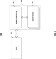
- FIG. 1 illustrates a block diagram of an exemplary system 100 having a memory device, according to some aspects of the present disclosure.
- System 100 can be a mobile phone, a desktop computer, a laptop computer, a tablet, a vehicle computer, a gaming console, a printer, a positioning device, a wearable electronic device, a smart sensor, a virtual reality (VR) device, an argument reality (AR) device, or any other suitable electronic devices having storage therein.
- system 100 can include a host 108 and a memory system 102 having one or more memory devices 104 and a memory controller 106.
- Host 108 can be a processor of an electronic device, such as a central processing unit (CPU), or a system-on-chip (SoC), such as an application processor (AP).
- Host 108 can be coupled to memory controller 106 and configured to send or receive data to or from memory devices 104 through memory controller 106. For example, host 108 may send the program data in a program operation or receive the read data in a read operation.
- Memory controller 106 is coupled to memory device 104 and host 108 and is configured to control memory device 104, according to some implementations. Memory controller 106 can manage the data stored in memory device 104 and communicate with host 108. In some implementations, memory controller 106 is designed for operating in a low duty-cycle environment like secure digital (SD) cards, compact Flash (CF) cards, universal serial bus (USB) Flash drives, or other media for use in electronic devices, such as personal computers, digital cameras, mobile phones, etc. In some implementations, memory controller 106 is designed for operating in a high duty-cycle environment SSDs or embedded multi-media-cards (eMMCs) used as data storage for mobile devices, such as smartphones, tablets, laptop computers, etc., and enterprise storage arrays.
- SSDs secure digital
- CF compact Flash
- USB universal serial bus
- Memory controller 106 can be configured to control operations of memory device 104, such as read, erase, and program operations, by providing instructions, such as read instructions, to memory device 104.
- memory controller 106 may be configured to provide a read instruction to the peripheral circuit of memory device 104 to control the read operation.
- Memory controller 106 can also be configured to manage various functions with respect to the data stored or to be stored in memory device 104 including, but not limited to bad-block management, garbage collection, logical-to-physical address conversion, wear leveling, etc.
- memory controller 106 is further configured to process error correction codes (ECCs) with respect to the data read from or written to memory device 104. Any other suitable functions may be performed by memory controller 106 as well, for example, formatting memory device 104.
- ECCs error correction codes
- Memory controller 106 can communicate with an external device (e.g., host 108) according to a particular communication protocol.
- memory controller 106 may communicate with the external device through at least one of various interface protocols, such as a USB protocol, an MMC protocol, a peripheral component interconnection (PCI) protocol, a PCI-express (PCI-E) protocol, an advanced technology attachment (ATA) protocol, a serial-ATA protocol, a parallel-ATA protocol, a small computer small interface (SCSI) protocol, an enhanced small disk interface (ESDI) protocol, an integrated drive electronics (IDE) protocol, a Firewire protocol, etc.
- various interface protocols such as a USB protocol, an MMC protocol, a peripheral component interconnection (PCI) protocol, a PCI-express (PCI-E) protocol, an advanced technology attachment (ATA) protocol, a serial-ATA protocol, a parallel-ATA protocol, a small computer small interface (SCSI) protocol, an enhanced small disk interface (ESDI) protocol, an integrated drive electronics (IDE) protocol, a Fire
- Memory controller 106 and one or more memory devices 104 can be integrated into various types of storage devices, for example, being included in the same package, such as a universal Flash storage (UFS) package or an eMMC package. That is, memory system 102 can be implemented and packaged into different types of end electronic products.
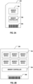
- memory controller 106 and a single memory device 104 may be integrated into a memory card 202.
- Memory card 202 can include a PC card (PCMCIA, personal computer memory card international association), a CF card, a smart media (SM) card, a memory stick, a multimedia card (MMC, RS-MMC, MMCmicro), an SD card (SD, miniSD, microSD, SDHC), a UFS, etc.
- Memory card 202 can further include a memory card connector 204 coupling memory card 202 with a host (e.g., host 108 in FIG. 1 ).
- memory controller 106 and multiple memory devices 104 may be integrated into an SSD 206.
- SSD 206 can further include an SSD connector 208 coupling SSD 206 with a host (e.g., host 108 in FIG. 1 ).
- the storage capacity and/or the operation speed of SSD 206 is greater than those of memory card 202.
- FIG. 3 illustrates a schematic circuit diagram of an exemplary memory device 300 including peripheral circuits, according to some aspects of the present disclosure.
- Memory device 300 can be an example of memory device 104 in FIG. 1 .
- Memory device 300 can include a memory cell array 301 and peripheral circuits 302 coupled to memory cell array 301.
- Memory cell array 301 can be a NAND Flash memory cell array in which memory cells 306 are provided in the form of an array of NAND memory strings 308 each extending vertically above a substrate (not shown).
- each NAND memory string 308 includes a plurality of memory cells 306 coupled in series and stacked vertically.
- Each memory cell 306 can hold a continuous, analog value, such as an electrical voltage or charge, which depends on the number of electrons trapped within a region of memory cell 306.
- Each memory cell 306 can be either a floating gate type of memory cell including a floating-gate transistor or a charge trap type of memory cell including a charge-trap transistor.
- each memory cell 306 is a single-level cell (SLC) that has two possible memory states and thus, can store one bit of data.
- the first memory state "0" can correspond to a first range of voltages
- the second memory state "1" can correspond to a second range of voltages.
- each memory cell 306 is a multi-level cell (MLC) that is capable of storing more than a single bit of data in more than four memory states.
- the MLC can store two bits per cell, three bits per cell (also known as triple-level cell (TLC)), or four bits per cell (also known as a quad-level cell (QLC)).
- TLC triple-level cell
- QLC quad-level cell
- Each MLC can be programmed to assume a range of possible nominal storage values. In one example, if each MLC stores two bits of data, then the MLC can be programmed to assume one of three possible programming levels from an erased state by writing one of three possible nominal storage values to the cell. A fourth nominal storage value can be used for the
- each NAND memory string 308 can include a source select gate (SSG) transistor 310 at its source end and a drain select gate (DSG) transistor 312 at its drain end.
- SSG transistor 310 and DSG transistor 312 can be configured to activate selected NAND memory strings 308 (columns of the array) during read and program operations.
- the sources of NAND memory strings 308 in the same block 304 are coupled through a same source line (SL) 314, e.g., a common SL.
- SL source line
- all NAND memory strings 308 in the same block 304 have an array common source (ACS), according to some implementations.
- ACS array common source
- each NAND memory string 308 is configured to be selected or deselected by applying a select voltage (e.g., above the threshold voltage of DSG transistor 312) or a deselect voltage (e.g., 0 V) to the gate of respective DSG transistor 312 through one or more DSG lines 313 and/or by applying a select voltage (e.g., above the threshold voltage of SSG transistor 310) or a deselect voltage (e.g., 0 V) to the gate of respective SSG transistor 310 through one or more SSG lines 315.
- a select voltage e.g., above the threshold voltage of DSG transistor 312
- a deselect voltage e.g., 0 V
- NAND memory strings 308 can be organized into multiple blocks 304, each of which can have a common source line 314, e.g., coupled to the ACS.
- each block 304 is the basic data unit for erase operations, i.e., all memory cells 306 on the same block 304 are erased at the same time.
- source lines 314 coupled to selected block 304 as well as unselected blocks 304 in the same plane as selected block 304 can be biased with an erase voltage (Vers), such as a high positive voltage (e.g., 20 V or more).
- Memory cells 306 of adjacent NAND memory strings 308 can be coupled through word lines 318 that select which row of memory cells 306 is affected by the read and program operations.
- each word line 318 is coupled to a page 320 of memory cells 306, which is the basic data unit for the program and read operations.
- the size of one page 320 in bits can relate to the number of NAND memory strings 308 coupled by word line 318 in one block 304.
- Each word line 318 can include a plurality of control gates (gate electrodes) at each memory cell 306 in respective page 320 and a gate line coupling the control gates.
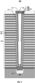
- FIG. 4 illustrates a side view of a cross-section of an exemplary memory cell array 301 including NAND memory strings 308, according to some aspects of the present disclosure.
- NAND memory string 308 can extend vertically through a memory stack 404 above a substrate 402.
- Substrate 402 can include silicon (e.g., single crystalline silicon), silicon germanium (SiGe), gallium arsenide (GaAs), germanium (Ge), silicon on insulator (SOI), germanium on insulator (GOI), or any other suitable materials.
- Memory stack 404 can include interleaved gate conductive layers 406 and gate-to-gate dielectric layers 408. The number of the pairs of gate conductive layers 406 and gate-to-gate dielectric layers 408 in memory stack 404 can determine the number of memory cells 306 in memory cell array 301.
- Gate conductive layer 406 can include conductive materials including, but not limited to, tungsten (W), cobalt (Co), copper (Cu), aluminum (Al), polysilicon, doped silicon, silicides, or any combination thereof.
- each gate conductive layer 406 includes a metal layer, such as a tungsten layer.
- each gate conductive layer 406 includes a doped polysilicon layer.
- Each gate conductive layer 406 can include control gates surrounding memory cells 306, the gates of DSG transistors 312, or the gates of SSG transistors 310, and can extend laterally as DSG line 313 at the top of memory stack 404, SSG line 315 at the bottom of memory stack 404, or word line 318 between DSG line 313 and SSG line 315.
- NAND memory string 308 includes a channel structure 412 extending vertically through memory stack 404.
- channel structure 412 includes a channel hole filled with semiconductor material(s) (e.g., as a semiconductor channel 420) and dielectric material(s) (e.g., as a memory film 418).
- semiconductor channel 420 includes silicon, such as polysilicon.
- memory film 418 is a composite dielectric layer including a tunneling layer 426, a storage layer 424 (also known as a "charge trap/storage layer”), and a blocking layer 422.
- Channel structure 412 can have a cylinder shape (e.g., a pillar shape).
- Tunneling layer 426 can include silicon oxide, silicon oxynitride, or any combination thereof.
- Storage layer 424 can include silicon nitride, silicon oxynitride, silicon, or any combination thereof.
- Blocking layer 422 can include silicon oxide, silicon oxynitride, high dielectric constant (high-k) dielectrics, or any combination thereof.
- memory film 418 may include a composite layer of silicon oxide/silicon oxynitride/silicon oxide (ONO).
- a well 414 (e.g., a P-well and/or an N-well) is formed in substrate 402, and the source end of NAND memory string 308 is in contact with well 414, according to some implementations.
- source line 314 may be coupled to well 414 to apply an erase voltage to well 414, i.e., the source of NAND memory string 308, during erase operations.
- NAND memory string 308 further includes a channel plug 416 at the drain end of NAND memory string 308.
- peripheral circuits 302 can be coupled to memory cell array 301 through bit lines 316, word lines 318, source lines 314, SSG lines 315, and DSG lines 313.
- Peripheral circuits 302 can include any suitable analog, digital, and mixed-signal circuits for facilitating the operations of memory cell array 301 by applying and sensing voltage signals and/or current signals to and from each target memory cell 306 through bit lines 316, word lines 318, source lines 314, SSG lines 315, and DSG lines 313.
- Peripheral circuits 302 can include various types of peripheral circuits formed using metal-oxide-semiconductor (MOS) technologies. For example, FIG.
- MOS metal-oxide-semiconductor
- FIG. 5 illustrates some exemplary peripheral circuits including a page buffer/sense amplifier 504, a column decoder/bit line driver 506, a row decoder/word line driver 508, a voltage generator 510, control logic 512, registers 514, an interface 516, and a data bus 518. It is understood that in some examples, additional peripheral circuits not shown in FIG. 5 may be included as well.
- Page buffer/sense amplifier 504 can be configured to read and program (write) data from and to memory cell array 301 according to the control signals from control logic 512.
- page buffer/sense amplifier 504 may store one page of program data (write data) to be programmed into one page 320 of memory cell array 301.
- page buffer/sense amplifier 504 may perform program verify operations to ensure that the data has been properly programmed into memory cells 306 coupled to selected word lines 318.
- page buffer/sense amplifier 504 may also sense the low power signals from bit line 316 that represents a data bit stored in memory cell 306 and amplifies the small voltage swing to recognizable logic levels in a read operation.
- page buffer/sense amplifier 504 can include a plurality of physically separated portions (e.g., four quarters) that can be sequentially accessed through its own clock path and data path in read operations.
- Row decoder/word line driver 508 can be configured to be controlled by control logic 512 according to the control signals from control logic 512 and select/deselect blocks 304 of memory cell array 301 and select/deselect word lines 318 of block 304. Row decoder/word line driver 508 can be further configured to drive word lines 318 using word line voltages generated from voltage generator 510. In some implementations, row decoder/word line driver 508 can also select/deselect and drive SSG lines 315 and DSG lines 313 as well.
- Voltage generator 510 can be configured to be controlled by control logic 512 according to the control signals from control logic 512 and generate the word line voltages (e.g., read voltage, program voltage, pass voltage, local voltage, verification voltage, etc.), bit line voltages, and source line voltages to be supplied to memory cell array 301.
- word line voltages e.g., read voltage, program voltage, pass voltage, local voltage, verification voltage, etc.
- Control logic 512 can be coupled to each peripheral circuit described above and configured to control the operations of each peripheral circuit by generating and sending various control signals, such as read commands for read operations. Control logic 512 can also send clock signals at desired frequencies, periods, and duty cycles to other peripheral circuits 302 to orchestrate the operations of each peripheral circuit 302, for example, for synchronization.
- Registers 514 can be coupled to control logic 512 and include status registers, command registers, and address registers for storing status information, command operation codes (OP codes), and command addresses for controlling the operations of each peripheral circuit 302.
- Interface 516 can be coupled to control logic 512 and act as an instruction fetcher/buffer as well as an instruction decoder to decode instructions received from a memory controller (e.g., 106 in FIG. 1 ) and relay the decoded instructions to control logic 512. Interface 516 can also buffer and relay status information received from control logic 512 to the memory controller (e.g., 106 in FIG. 1 ). Interface 516 can be coupled to page buffer/sense amplifier 504 via data bus 518 and further act as a data input/output (I/O) interface and a data buffer to buffer and relay the data to and from memory cell array 301.
- I/O data input/output
- peripheral circuits 302 can further include a clock path 520 coupled to and from each portion of page buffer/sense amplifier 504 and configured to transfer and merge multiple clock return signals from multiple portions of page buffer/sense amplifier 504 in a read operation according to the clock signal return schemes disclosed herein.
- Clock path 520 can be coupled to interface 516 as well to transfer the merged clock return signals to interface 516 in order to synchronize the output of the read-out data from data bus 518 in read operations.
- the merged clock return signal on clock path 520 is aligned with the read-out data on data bus 518 in a read operation.
- FIG. 6 illustrates a block diagram of exemplary memory device 300 including multiple memory planes, according to some aspects of the present disclosure.
- memory device 300 includes a plurality of memory planes 602 (e.g., four memory planes in FIG. 6 ).
- Memory plane 602 can be mutually independent in performing a read operation, a program operation, or an erase operation.
- each memory plane 602 may be configured to perform a read operation independently in response to receiving a read control signal from control logic 512.
- each memory plane 602 covers local buffering for the read and program data and can process operations in parallel, thereby increasing the operation speed.
- each memory plane 602 can include a set of blocks 304 of memory cell array 301 and a set of peripheral circuits, such as page buffer/sense amplifier 504, column decoder/bit line driver 506, and row decoder/word line driver 508.
- FIG. 7 illustrates an exemplary layout of memory plane 602 including page buffer/sense amplifier 504 having multiple portions and clock path 520 coupled to the multiple portions of page buffer/sense amplifier 504, according to some aspects of the present disclosure.
- Memory plane 602 can include page buffer/sense amplifier 504 divided into a plurality of portions.
- page buffer/sense amplifier 504 includes four physically separated quarters 504a, 504b, 504c, and 504d, according to some implementations.
- the multiple portions of a page buffer may be described herein as four quarters. It is understood that the number of portions is not limited to four and may be any integer greater than 1 (e.g., 2, 3, 4, 5, 6, etc.), for example, two halves.
- Page buffer/sense amplifier 504 can include a plurality of storage units (e.g., latches, caches, or registers) for temporarily storing (buffering) one or more pages of data to be read from or written to the memory cells in memory plane 602.
- each quarter 504a, 504b, 504c, or 504d has the same size, i.e., one quarter of page buffer/sense amplifier 504.
- page buffer/sense amplifier 504 may store 16K bytes of data
- each quarter 504a, 504b, 504c, or 504d may store 4K bytes of data.
- clock path 520 is coupled to each quarter 504a, 504b, 504c, or 504d of page buffer/sense amplifier 504. As shown in FIG. 7 , clock path 520 can diverge at each junction 702, 704a, or 704b to form branches thereof. For example, clock path 520 may diverge into two plane half branches at junction 702, and each plane half branch of clock path may respectively diverge into two quarter branches at a respective junction 704a or 704b, such that each of four quarter branches of clock path 520 may be coupled to a respective quarter 504a, 504b, 504c, or 504d of page buffer/sense amplifier 504.
- Clock path 520 can be bidirectional to transfer clock signals from, for example, control logic 512, to each quarter 504a, 504b, 504c, or 504d, and transfer clock return signals from each quarter 504a, 504b, 504c, or 504d to, for example, interface 516.
- clock path 520 is configured to split a clock signal into four clock signals and transfer the four clock signals to four quarters 504a, 504b, 504c, and 504d of page buffer/sense amplifier 504, respectively, via the quarter branches thereof.
- clock path 520 is also configured to transfer four clock return signals from four quarters 504a, 504b, 504c, and 504d of page buffer/sense amplifier 504, respectively, via the quarter branches thereof, and merge the four clock return signals into a merged clock return signal.
- FIG. 8 illustrates a circuit diagram of a clock path 800 coupled to multiple portions of a page buffer 801 for merging clock return signals.
- FIG. 9 illustrates a timing diagram of a clock signal return scheme implemented by clock path 800 in FIG. 8 .
- Each of quarters 0, 1, 2, and 3 of page buffer 801 is sequentially selected following this order: 0, 1, 2, and 3 in a read operation.
- the clock signal (clk_dp) transferred on clock path 800 to page buffer 801 is split into two sequential clock signals (clk_dp_q0 and clk_dp_q1).
- each of quarters 0 and 1 sequentially receives a respective clock signal (clk_dp_q0 or clk_dp_q1).
- a respective clock signal 802 passes through a respective delay circuit (DLY) 804 to become a respective clock return signal (clk_rtn_q0, clk_rtn_q1, clk_rtn_q2, or clk_rtn_q3) in a respective branch of clock path 800.
- DLY delay circuit
- delay circuit 804 for quarter 0 acts as a frequency multiplier to reduce the period of the first clock return signal (clk_rtn_q0) from that of the first clock signal (clk_dp_q0).
- delay circuit 804 for quarter 1 acts as a frequency multiplier to reduce the period of the second clock return signal (clk_rtn_q1) from that of the second clock signal (clk_dp_q1).
- clock return signals are transferred on clock path 800 in the forms of short pulses to ensure that the end level of each clock return signal when switching is low (e.g., 0 V, Vss) to avoid gating each other when merging at quarter branches of clock path 800 by OR gates 806.
- end level of each clock return signal when switching is low (e.g., 0 V, Vss) to avoid gating each other when merging at quarter branches of clock path 800 by OR gates 806.
- delay circuit 804 is shown in page buffer 801 of FIG. 8
- any other suitable components for example, as described above, may be included in each quarter of page buffer 801.
- each quarter branch of clock path 800 every two clock return signals from two quarters next to each other (e.g., quarters 0 and 1, or quarters 2 and 3) are merged by a respective OR gate 806.
- Each of the two merged clock return signals on a respective quarter branch of clock path 800 also passes a respective frequency divider 808 that increases its period to generate a respective merged clock return signal (clk_rtn_q01 or clk_rtn_q23).
- OR gate 806 in conjunction with frequency divider 808 toggle the level of the merged clock return signal (clk_rtn_q01) at each rising edge of either clock return signal (clk_rtn_q0 or clk_rtn_q1). In other words, the short pulse of each clock return signal is enlarged after merging at each quarter branch.
- clock path 800 since the two merged clock return signals (clk_rtn_q01 or clk_rtn_q23) need to merge again in the plane half branch, clock path 800 also includes an edge detector/pulse generator 810 on each quarter branch that respectively generates a short pulse at each rising edge or falling edge of a respective merged clock return signal (clk_rtn_q01 or clk_rtn_q23). The two outputted signals are merged again by an OR gate 812 to generate a merged clock return signal (clk_rtn_pul). As shown in FIG.
- short pulses are regenerated in the merged clock return signal (clk_rtn_pul) in response to the rising edges or falling edges of the merged clock return signal (clk_trn_q01).
- the merged clock return signal (clk_rtn_pul) needs to pass through a frequency divider 814 again on clock path 800 to increase the period, i.e., enlarging the short pulses, of the merged clock return signal (clk_rtn).
- the frequent change of the signal periods and frequencies over clock path 800 is also undesirable as it can increase the risk of mismatch between clock return signals and the corresponding data signals.
- an improved clock signal return scheme is disclosed herein with respect to FIGs. 10 and 11 below.
- the clock return signal returned from the current select portion can be ensured to finish at a particular level (e.g., low for OR gate and high for NAND gate) that will not gate another clock return signal next to it.
- a frequency divider can be used at the beginning of the clock path to increase the period of the clock return signal to avoid using short pulses for clock return signals. For example, FIG.
- FIG. 10 illustrates a circuit diagram of an exemplary clock level set module 1004 and an exemplary clock path 1002 each coupled to multiple portions of a page buffer 1001 for merging clock return signals, according to some aspects of the present disclosure
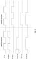
- FIG. 11 illustrates a timing diagram of an exemplary clock signal return scheme implemented by clock path 1002 in FIG. 10 , according to some aspects of the present disclosure.
- Clock path 1002 and clock level set module 1004 can be parts of peripheral circuits 302 of memory device 300.
- Clock path 1002 may be one example of clock path 520 in FIG. 5 .
- clock level set module 1004 is illustrated and described herein as a separate component coupled to page buffer 1001, clock level set module 1004 may be a standalone circuit or part of another peripheral circuit 302, such as part of page buffer 1001. For example, clock level set module 1004 may be part of page buffer/sense amplifier 504 or part of control logic 512 in FIG. 5 .
- Page buffer 1001 described with respect to FIGs. 10 and 11 may be, for example, page buffer/sense amplifier 504 in FIGs. 5-7 that includes a plurality of portions, such as four quarters 504a, 504b, 504c, and 504d in FIG. 7 .
- Each quarter 504a, 504b, 504c, or 504d can be configured to sequentially receive a clock signal.
- a clock signal (clk_dp) may be transferred from control logic 512 to page buffer/sense amplifier 504 and split into four clock signals (clk_dp_q0, clk_dp_q1, clk_dp_q2, and clk_dp_q3) by junctions 702, 704a, and 704b of clock path 520, which are respectively transferred to quarters 504a, 504b, 504c, and 504d through four quarter branches. Taking quarters 0 and 1 as an example, as shown in FIG. 11 , quarter 0 may be first selected and receives a first clock signal (clk_dp_q0) of the clock signal (clk_dp) in a read operation.
- the current selected quarter may change from quarter 0 to quarter 1, which receives a second clock signal (clk_dp_q1) of the clock signal (clk_dp).
- the clock signal timing may be similarly applied to quarters 2 and 3 when they are selected.
- the sequence of selecting each quarter i.e., the sequence of receiving clock signals by the four quarters, may be preset, for example, in the order of quarters 0, 1, 2, and 3. It is further understood that depending on the specific read instruction, in a read operation, not all four quarters may always be selected.
- the first selected quarter may be any one of quarters 0, 1, 2, and 3.
- the last selected quarter may be any one of quarters 0, 1, 2, and 3.
- Each quarter 504a, 504b, 504c, or 504d can also be configured to sequentially return a clock return signal in response to receiving the corresponding clock signal. That is, in some implementations, each quarter 504a, 504b, 504c, or 504d returns a clock return signal once the corresponding clock signal is received, i.e., following the wave pipeline structure as described above.
- the sequence of returning the clock return signals by the four quarters can thus be the same as the sequence of receiving the clock signals by the four quarters, as well as the sequence of selecting each quarter. It is understood that the sequence of returning the clock return signals by the four quarters may be thus preset as well, for example, in the order of quarters 0, 1, 2, and 3.
- clock path 1002 is coupled to the plurality of portions of page buffer 1001 and configured to merge the plurality of clock return signals.
- clock path 1002 may be coupled to the four quarters of page buffer 1001 and configured to merge the four clock return signals sequentially returned from the four quarters. It is understood that in some examples, not all four quarters may be selected in a read operation depending on the read instructions and thus, clock path 1002 may merge only some of the four clock return signals accordingly in those examples. Nevertheless, clock path 1002 can be capable of merging all four clock return signals sequentially returned from the four quarters when the four quarters are all selected in read operations.
- clock level set module 1004 is coupled to each quarter of page buffer 1001 and configured to set the start level of a first clock return signal of the plurality of clock return signals based on the number of cycles in a first clock signal of the plurality of clock signals.
- the first clock return signal can correspond to the first clock signal.
- the first clock signal is sent to the current selected portion of page buffer 1001 in a read operation based on the read instruction, and the first clock return signal is returned by the current selected portion of page buffer 1001 in response to receiving the first clock signal, according to some implementations.
- the end level of the first clock return signal can be set at a level that would not gate the second clock return signal next to the first clock return signal when the first and second clock return signals are merged by clock path 1002, as described below in detail.
- each quarter of page buffer 1001 includes a frequency divider 1012 coupled to clock level set module 1004.
- Each frequency divider 1012 can be configured to receive a respective clock signal 1010 (e.g., clk_dp_q0 or clk_dp_q1 in FIG. 11 ) and generate the respective clock return signal (clk_rtn_q0, clk_rtn_q1, clk_rtn_q2, or clk_rtn_q3) based on clock signal 1010.
- frequency divider 1012 includes a flip-flop 1014 coupled to clock level set module 1004.
- flip-flop 1014 may be a D flip-flop (DFF) with set/reset (SR).
- the DFF with SR may include a clock input, an SR input, a D input, a Q output and a Q output.
- the Q output of the DFF may be coupled to the D input via an inverter, and the Q output of the DFF may output the respective clock return signal (clk_rtn_q0, clk_rtn_q1, clk_rtn_q2, or clk_rtn_q3).
- the clock input of the DFF may receive the respective clock signal (clk_dp_q0, clk_dp_q1, clk_dp_q2, or clk_dp_q3), and the SR input of the DFF may receive an SR signal from clock level set module 1004. Also referring to FIG. 11 , taking quarters 0 and 1, for example, when quarter 0 is selected, frequency divider 1012 coupled to quarter 0 can double the period of the first clock return signal (clk_rtrn_q0) from the period of the first clock signal (clk_dp_q0) to avoid transferring short pulses on clock path 1002.
- the duty cycle of the first clock return signal (clk_rtrn_q0) may be 50%.
- frequency divider 1012 coupled to quarter 1 can double the period of the second clock return signal (clk_rtrn_q1) from the period of the second clock signal (clk_dp_q1) as well. It is understood although only frequency divider 1012 coupled to one of the quarters of page buffer 1001 is shown in FIG. 10 for ease of illustration, frequency divider 1012 may be similarly coupled to each of the four quarters of page buffer 1001.
- clock level set module 1004 in conjunction with frequency dividers 1012 can ensure that the end level of the clock return signal is at a level (either at a high level, e.g., Vdd, or at a low level, e.g., 0 V or Vss) that would not gate the subsequent clock return signal by setting the suitable start level of the clock return signal.
- clock level set module 1004 is configured to determine the parity of the number of cycles in the first clock signal based on an address of the page buffer associated with the first clock signal, and set the start level of the first clock return signal based on the parity.
- the address can be in a read instruction. Since the level of the clock return signal is toggled at each rising edge of the respective clock signal by frequency divider 1012, the parity (odd or even) of the number of cycles in the clock signal, as well as the start level (high or low) of the clock return signal determine the end level (high or low) of the clock return signal, according to some implementations.
- the start and end levels of the clock return signal may be the same if the parity of the number of cycles in the clock signal is even, while the start and end levels of the clock return signal may be different if the parity of the number of cycles in the clock signal is odd.
- clock level set module 1004 includes an address unit 1006 configured to receive a read instruction or a read command including the starting address of the data to be read from page buffer/sense amplifier 504, and determine the parity of the number of cycles in the clock signal.
- clock level set module 1004 can be part of page buffer/sense amplifier 504, for example, as a dedicated integrated circuit (IC), such as an application-specific integrated circuit (ASIC), or can be part of control logic 512, for example, as a dedicated IC or firmware/software code running on a microcontroller unit (MCU).
- address unit 1006 can either receive the read instruction from a memory controller (e.g., 106 in FIG.
- address unit 1006 is capable of identifying the starting address of the data to be read in the read operation in one of the four quarters of page buffer/sense amplifier 504.
- the number of cycles in the first clock signal corresponds to the number of data units transferred in the corresponding portion of page buffer 1001 with the first clock signal. That is, the clock signals can be synchronized with the data signals.
- address unit 1006 can determine the number of cycles in the clock signal sent to the current selected quarter.
- address unit 1006 determines the parity based on the lowest bit of the address of the read data in a read instruction.
- the starting address may be in quarter 0, which becomes the first select quarter.
- clock level set module 1004 may determine that there is an odd number (1) of cycle in the clock signal sent to quarter 0, which will make the start and end levels of the clock return signal from quarter 0 to be different.
- clock level set module 1004 may determine that there is an even number (4 or 12) of cycles in the clock signal coupled to quarter 0, which will make the start and end levels of the clock return signal from quarter 0 to be the same. It is understood that the starting address may not always be in quarter 0.
- the starting address may be in quarter 1
- clock level set module 1004 may determine that there is an even number (6) of cycles in the clock signal coupled to quarter 1, which will make the start and end levels of the clock return signal from quarter 1 to be the same.
- clock level set module 1004 includes an SR unit 1008 configured to generate the SR signal to the SR input of flip-flop 1014 based on the parity of the number of cycles in the clock signal.
- SR unit 1008 configured to generate the SR signal to the SR input of flip-flop 1014 based on the parity of the number of cycles in the clock signal.
- the start level of the output i.e., the first clock return signal
- Clock path 1002 can include either an OR gate or a NAND gate configured to merge two clock return signals.
- clock level set module 1004 can be further configured to set the start level of the first clock return signal based on the parity and whether the clock return signals are merged by the OR gate or the NAND gate. Gating may occur at an OR gate when the end level of first clock return signal is high, or at a NAND gate when the end level of the first clock return signal is low. In some implementations, the end level of the first clock return signal is low in response to clock path 1002 including an OR gate to avoid gating at the OR gate. In some implementations, the end level of the first clock return signal is high in response to clock path 1002 including a NAND gate to avoid gating at the NAND gate.
- clock path 1002 includes two OR gates 1018 each configured to merge two clock return signals (clk_rtn_q0 and clk_rtn_q1, or clk_rtn_q2 and clk_rtn_q3) and generate a merged clock return signal (clk_rtn_q01 or clk_rtn_q23).
- clock return signals clk_rtn_q0 and clk_rtn_q1, or clk_rtn_q2 and clk_rtn_q3
- the start level of the first clock return signal (clk_rtn_q0) may be set to low, such that the end level of the first clock return signal (clk_rtn_q0) may remain low to avoid gating the second clock return signal (clk_rtn_q0) next to the first clock return signal (clk_rtn_q0).
- the merged clock return signal (clk_rtn_q01) may be generated without the concern of gating even when short pulses are not used in the first or second clock return signal (clk_rtn_q0 or clk_rtn_q1).
- clock level set module 1004 is further configured to set the start level of a second clock return signal next to the first clock return signal to low in response to clock path 1002 including an OR gate, and set the start level of the second clock return signal to high in response to clock path 1002 including a NAND gate.
- clock level set module 1004 can determine the start level of the corresponding clock return signal based on whether the first and second clock return signals are merged by an OR gate or AND gate alone. In case the data transferred in the subsequent quarter may not occupy the entire quarter, i.e., no further quarter and clock return signals may be needed in the read operation, the gating would not be an issue for the second clock return signal then since no more merging is needed.
- clock level set module 1004 may set the start level of each clock return signal from quarter 1, 2, or 3 to low.
- clock level set module 1004 may set the start level of the clock return signal from quarter 2 to low.
- clock path 1002 can further include an OR gate 1020 configured to further merge the two merged clock return signals (clk_rtn_q01 and clk_rtn_q23) to generate a merged clock return signal (clk_rtn) that merges the four clock return signals (clk_rtn_q0, clk_rtn_q1, clk_rtn_q2, and clk_rtn_q3) from the four quarters.
- OR gate 1020 configured to further merge the two merged clock return signals (clk_rtn_q01 and clk_rtn_q23) to generate a merged clock return signal (clk_rtn) that merges the four clock return signals (clk_rtn_q0, clk_rtn_q1, clk_rtn_q2, and clk_rtn_q3) from the four quarters.
- clock path 1002 further includes one or more delay circuits, for example, a delay circuit 1016 after each frequency divider 1012, and a delay circuit 1022 after OR gate 1020, to synchronize the clock return signals with corresponding data signals in case a misalignment occurs during the transfer of the clock return signals by clock path 1002.
- the merged clock return signal (clk_rtn) may become a synchronized merged clock return signal (clk_rtn_srync) after passing delay circuit 1022 to be used for reading the aligned data signals.
- FIG. 13 illustrates a flowchart of a method 1300 for operating a memory device, according to some aspects of the present disclosure.
- the memory device may be any suitable memory device disclosed herein, such as memory device 300.
- Method 1300 may be implemented by clock level set module 1004. It is understood that the operations shown in method 1300 may not be exhaustive and that other operations can be performed as well before, after, or between any of the illustrated operations. Further, some of the operations may be performed simultaneously, or in a different order than shown in FIG. 13 .
- method 1300 starts at operation 1302, in which a read instruction is received.
- control logic 512 of memory device 300 may receive a read instruction from memory controller 106 in a read operation.
- Method 1300 proceeds to operation 1304, as illustrated in FIG. 13 , in which an address of the page buffer is obtained in the read instruction.
- clock level set module 1004 of memory device 300 may obtain the starting address of data to be read from page buffer/sense amplifier 504 in the read instruction.
- Method 1300 proceeds to operation 1306, as illustrated in FIG. 13 , in which a parity of a number of cycles in a first clock signal is determined based on the address. The first clock signal is received by a first portion of the page buffer.
- the number of cycles in the first clock signal can correspond to a number of data units transferred in the first portion of the page buffer with the first clock signal.
- clock level set module 1004 of memory device 300 may determine the parity of the number of cycles in the clock signal sent to the current select quarter based on the starting address.
- Method 1300 proceeds to operation 1308, as illustrated in FIG. 13 , in which a start level of a first clock return signal is set based on the parity.
- the first clock return signal is returned by the first portion of the page buffer in response to receiving the first clock signal.
- the duty cycle of the first clock return signal can be 50%.
- clock level set module 1004 and frequency divider 1012 of memory device 300 may set the start level of the clock return signal from the current select quarter based on the parity.
- Method 1300 proceeds to operation 1310, as illustrated in FIG. 13 , in which a start level of a second clock return signal is set to be a same level as an end level of the first clock return signal.
- the second clock return signal is returned next to the first clock return signal by a second portion of the page buffer.
- clock level set module 1004 and another frequency divider 1012 of memory device 300 may set the start level of the subsequent clock return signal from the next select quarter to be the same level as the end level of the clock return signal.
- a circuit includes a page buffer including a plurality of portions, a clock path coupled to the plurality of portions of the page buffer, and a clock level set module coupled to the page buffer.
- Each of the portions is configured to sequentially receive a clock signal, and sequentially return a clock return signal in response to receiving the corresponding clock signal.
- the clock path is configured to merge the plurality of clock return signals.
- the clock level set module is configured to set a start level of a first clock return signal of the plurality of clock return signals based on a number of cycles in a first clock signal of the plurality of clock signals. The first clock return signal corresponds to the first clock signal.
- the clock level set module is configured to determine a parity of the number of cycles in the first clock signal based on an address of the page buffer associated with the first clock signal, and set the start level of the first clock return signal based on the parity.
- the address is in a read instruction.
- the clock path includes an OR gate or a NAND gate configured to merge the plurality of clock return signals.
- an end level of the first clock return signal is low in response to the clock path including the OR gate, and the end level of the first clock return signal is high in response to the clock path including the NAND gate.
- the clock level set module is further configured to set a start level of a second clock return signal of the plurality of clock return signals to low in response to the clock path including the OR gate, and set the start level of the second clock return signal to high in response to the clock path including the NAND gate.
- the second clock return signal can be returned next to the first clock return signal.
- each portion of the page buffer includes a frequency divider configured to receive the respective clock signal and generate the respective clock return signal based on the clock signal.
- each frequency divider includes a flip-flop coupled to the clock level set module.
- the flip-flop includes a clock input receiving the respective clock signal, and a set/reset input receiving a set/reset signal from the clock level set module.
- a duty cycle of the first clock return signal is 50%.
- the number of cycles in the first clock signal corresponds to a number of data units transferred in the corresponding portion of the page buffer with the first clock signal.
- a system includes a memory device including a memory cell array configured to store data, and a peripheral circuit coupled to the memory cell array and configured to perform a read operation on the memory cell array to read the stored data.
- the peripheral circuit includes a page buffer including a plurality of portions, a clock path coupled to the plurality of portions of the page buffer, and a clock level set module coupled to the page buffer. Each of the portions is configured to sequentially receive a clock signal, and sequentially return a clock return signal in response to receiving the corresponding clock signal.
- the clock path is configured to merge the plurality of clock return signals.
- the clock level set module is configured to set a start level of a first clock return signal of the plurality of clock return signals based on a number of cycles in a first clock signal of the plurality of clock signals. The first clock return signal corresponds to the first clock signal.
- the system includes a memory controller coupled to the memory device and configured to provide a read instruction to the peripheral circuit to control the read operation.
- the system includes a host coupled to the memory controller and configured to receive the read data.
- the clock level set module is configured to determine a parity of the number of cycles in the first clock signal based on an address of the page buffer associated with the first clock signal, and set the start level of the first clock return signal based on the parity.
- the address is in a read instruction.
- the clock path includes an OR gate or a NAND gate configured to merge the plurality of clock return signals.
- an end level of the first clock return signal is low in response to the clock path including the OR gate, and the end level of the first clock return signal is high in response to the clock path including the NAND gate.
- the clock level set module is further configured to set a start level of a second clock return signal of the plurality of clock return signals to low in response to the clock path including the OR gate, and set the start level of the second clock return signal to high in response to the clock path including the NAND gate.
- the second clock return signal can be returned next to the first clock return signal.
- each portion of the page buffer includes a frequency divider configured to receive the respective clock signal and generate the respective clock return signal based on the clock signal.
- each frequency divider includes a flip-flop coupled to the clock level set module.
- the flip-flop includes a clock input receiving the respective clock signal, and a set/reset input receiving a set/reset signal from the clock level set module.
- a duty cycle of the first clock return signal is 50%.
- the number of cycles in the first clock signal corresponds to a number of data units transferred in the corresponding portion of the page buffer with the first clock signal.
- a memory device includes a memory cell array configured to store data, and a peripheral circuit coupled to the memory cell array and configured to perform a read operation on the memory cell array to read the stored data.
- the peripheral circuit includes a page buffer including a plurality of portions, a clock path coupled to the plurality of portions of the page buffer, and a clock level set module coupled to the page buffer. Each of the portions is configured to sequentially receive a clock signal, and sequentially return a clock return signal in response to receiving the corresponding clock signal.
- the clock path is configured to merge the plurality of clock return signals.
- the clock level set module is configured to set a start level of a first clock return signal of the plurality of clock return signals based on a number of cycles in a first clock signal of the plurality of clock signals. The first clock return signal corresponds to the first clock signal.
- a method for operating a memory device includes a page buffer.
- a read instruction is received.
- An address of the page buffer in the read instruction is obtained.
- a parity of a number of cycles in a first clock signal is determined based on the address.
- the first clock signal is received by a first portion of the page buffer.
- a start level of a first clock return signal is set based on the parity.
- the first clock return signal is returned by the first portion of the page buffer in response to receiving the first clock signal.
- a start level of a second clock return signal is set to be a same level as an end level of the first clock return signal.
- the second clock return signal can be returned next to the first clock return signal by a second portion of the page buffer.
- a duty cycle of the first clock return signal is 50%.
- the number of cycles in the first clock signal corresponds to a number of data units transferred in the first portion of the page buffer with the first clock signal.
Landscapes
- Engineering & Computer Science (AREA)
- Microelectronics & Electronic Packaging (AREA)
- Read Only Memory (AREA)
- Dram (AREA)
Priority Applications (1)
| Application Number | Priority Date | Filing Date | Title |
|---|---|---|---|
| EP25166295.3A EP4554350A3 (de) | 2021-04-28 | 2021-04-28 | Taktsignalrückführungsschema zum lesen von daten im seitenpuffer einer speichervorrichtung |
Applications Claiming Priority (3)
| Application Number | Priority Date | Filing Date | Title |
|---|---|---|---|
| PCT/CN2021/090444 WO2022226820A1 (en) | 2021-04-28 | 2021-04-28 | Clock signal return scheme for data read in page buffer of memory device |
| EP25166295.3A EP4554350A3 (de) | 2021-04-28 | 2021-04-28 | Taktsignalrückführungsschema zum lesen von daten im seitenpuffer einer speichervorrichtung |
| EP21938306.4A EP4200851B1 (de) | 2021-04-28 | 2021-04-28 | Taktsignalrückführungsschema zum lesen von daten im seitenpuffer einer speichervorrichtung |
Related Parent Applications (2)
| Application Number | Title | Priority Date | Filing Date |
|---|---|---|---|
| EP21938306.4A Division-Into EP4200851B1 (de) | 2021-04-28 | 2021-04-28 | Taktsignalrückführungsschema zum lesen von daten im seitenpuffer einer speichervorrichtung |
| EP21938306.4A Division EP4200851B1 (de) | 2021-04-28 | 2021-04-28 | Taktsignalrückführungsschema zum lesen von daten im seitenpuffer einer speichervorrichtung |
Publications (2)
| Publication Number | Publication Date |
|---|---|
| EP4554350A2 true EP4554350A2 (de) | 2025-05-14 |
| EP4554350A3 EP4554350A3 (de) | 2025-07-23 |
Family
ID=77577312
Family Applications (2)
| Application Number | Title | Priority Date | Filing Date |
|---|---|---|---|
| EP21938306.4A Active EP4200851B1 (de) | 2021-04-28 | 2021-04-28 | Taktsignalrückführungsschema zum lesen von daten im seitenpuffer einer speichervorrichtung |
| EP25166295.3A Pending EP4554350A3 (de) | 2021-04-28 | 2021-04-28 | Taktsignalrückführungsschema zum lesen von daten im seitenpuffer einer speichervorrichtung |
Family Applications Before (1)
| Application Number | Title | Priority Date | Filing Date |
|---|---|---|---|
| EP21938306.4A Active EP4200851B1 (de) | 2021-04-28 | 2021-04-28 | Taktsignalrückführungsschema zum lesen von daten im seitenpuffer einer speichervorrichtung |
Country Status (7)
| Country | Link |
|---|---|
| US (2) | US11694752B2 (de) |
| EP (2) | EP4200851B1 (de) |
| JP (2) | JP7510012B2 (de) |
| KR (1) | KR102811361B1 (de) |
| CN (1) | CN113383388B (de) |
| BR (1) | BR112023012414A2 (de) |
| WO (1) | WO2022226820A1 (de) |
Families Citing this family (2)
| Publication number | Priority date | Publication date | Assignee | Title |
|---|---|---|---|---|
| US11854660B2 (en) * | 2021-12-20 | 2023-12-26 | Nvidia Corp. | Slew signal shaper circuit using two signal paths |
| CN119673233A (zh) | 2023-09-20 | 2025-03-21 | 长江存储科技有限责任公司 | 存储器系统及其操作方法 |
Family Cites Families (27)
| Publication number | Priority date | Publication date | Assignee | Title |
|---|---|---|---|---|
| HU206367B (en) * | 1988-04-30 | 1992-10-28 | Sandoz Ag | Process for producing acid addition salts of steroid carboxylic acid-amidated taurine and glycine, as well as pharmaceutical compositions comprising such salts |
| JPH0836886A (ja) * | 1994-07-22 | 1996-02-06 | Nec Kagoshima Ltd | メモリ装置 |
| JP2960314B2 (ja) * | 1994-09-30 | 1999-10-06 | 川崎製鉄株式会社 | 半導体集積回路 |
| US5784332A (en) * | 1996-12-12 | 1998-07-21 | Micron Technology Corporation | Clock frequency detector for a synchronous memory device |
| CA2805213A1 (en) * | 1998-04-01 | 1999-10-01 | Mosaid Technologies Incorporated | Semiconductor memory asynchronous pipeline |
| US6445644B2 (en) * | 1998-05-20 | 2002-09-03 | Micron Technology, Inc. | Apparatus and method for generating a clock within a semiconductor device and devices and systems including same |
| US7319728B2 (en) | 2002-05-16 | 2008-01-15 | Micron Technology, Inc. | Delay locked loop with frequency control |
| JP2005182872A (ja) * | 2003-12-17 | 2005-07-07 | Toshiba Corp | 不揮発性半導体記憶装置 |
| JP2005339310A (ja) | 2004-05-28 | 2005-12-08 | Renesas Technology Corp | 半導体装置 |
| KR100626377B1 (ko) | 2004-06-07 | 2006-09-20 | 삼성전자주식회사 | 동작 모드에 따라 프로그램 전압의 증가분을 가변할 수있는 불 휘발성 메모리 장치 |
| CN100558032C (zh) * | 2005-01-24 | 2009-11-04 | 华为技术有限公司 | 访问缓存的方法 |
| KR100604948B1 (ko) * | 2005-08-17 | 2006-07-31 | 삼성전자주식회사 | 동기식 메모리장치의 웨이브 파이프라인 구조의 출력회로 |
| TW200910373A (en) | 2007-06-08 | 2009-03-01 | Mosaid Technologies Inc | Dynamic impedance control for input/output buffers |
| JP5097573B2 (ja) * | 2008-02-25 | 2012-12-12 | ルネサスエレクトロニクス株式会社 | 分周回路 |
| KR101027759B1 (ko) * | 2009-12-22 | 2011-04-07 | 연세대학교 산학협력단 | 지연 동기 루프 및 그것의 듀티 사이클 보정 회로 |
| KR102190962B1 (ko) * | 2013-12-30 | 2020-12-14 | 삼성전자주식회사 | 코맨드 처리 회로 및 이를 포함하는 메모리 장치 |
| CN107547087B (zh) * | 2016-06-29 | 2020-11-24 | 澜起科技股份有限公司 | 用于减少合成的时钟信号的失配的电路和方法 |
| US10156887B2 (en) * | 2016-09-29 | 2018-12-18 | Qualcomm Incorporated | Cache memory clock generation circuits for reducing power consumption and read errors in cache memory |
| CN108572785B (zh) * | 2017-03-08 | 2021-11-02 | 北京兆易创新科技股份有限公司 | 一种nand-flash存储器读操作方法及装置 |
| US10360956B2 (en) * | 2017-12-07 | 2019-07-23 | Micron Technology, Inc. | Wave pipeline |
| US10410698B2 (en) * | 2017-12-07 | 2019-09-10 | Micron Technology, Inc. | Skew reduction of a wave pipeline in a memory device |
| KR20190068094A (ko) * | 2017-12-08 | 2019-06-18 | 삼성전자주식회사 | 반도체 메모리 장치 및 메모리 시스템 |
| US10762947B2 (en) | 2018-10-04 | 2020-09-01 | Samsung Electronics Co., Ltd. | Memory devices |
| WO2020223844A1 (en) | 2019-05-05 | 2020-11-12 | Yangtze Memory Technologies Co., Ltd. | Double data rate circuit and data generation method implementing precise duty cycle control |
| KR20210034219A (ko) * | 2019-09-20 | 2021-03-30 | 에스케이하이닉스 주식회사 | 신호 생성 회로 및 이를 이용하는 반도체 장치 |
| WO2021210090A1 (ja) | 2020-04-15 | 2021-10-21 | 三菱電機株式会社 | 遅延同期回路及びクロック送信回路 |
| KR102949931B1 (ko) * | 2020-06-15 | 2026-04-09 | 삼성전자주식회사 | 불휘발성 메모리 장치, 및 그것의 동작 방법 |
-
2021
- 2021-04-28 JP JP2023534310A patent/JP7510012B2/ja active Active
- 2021-04-28 CN CN202180001162.5A patent/CN113383388B/zh active Active
- 2021-04-28 BR BR112023012414A patent/BR112023012414A2/pt unknown
- 2021-04-28 EP EP21938306.4A patent/EP4200851B1/de active Active
- 2021-04-28 EP EP25166295.3A patent/EP4554350A3/de active Pending
- 2021-04-28 KR KR1020237019061A patent/KR102811361B1/ko active Active
- 2021-04-28 WO PCT/CN2021/090444 patent/WO2022226820A1/en not_active Ceased
- 2021-05-28 US US17/334,131 patent/US11694752B2/en active Active
-
2023
- 2023-05-15 US US18/197,526 patent/US12183404B2/en active Active
-
2024
- 2024-06-17 JP JP2024097501A patent/JP7736865B2/ja active Active
Also Published As
| Publication number | Publication date |
|---|---|
| JP2024123102A (ja) | 2024-09-10 |
| CN113383388B (zh) | 2022-08-16 |
| JP7736865B2 (ja) | 2025-09-09 |
| BR112023012414A2 (pt) | 2023-11-07 |
| EP4200851A1 (de) | 2023-06-28 |
| WO2022226820A1 (en) | 2022-11-03 |
| US12183404B2 (en) | 2024-12-31 |
| CN113383388A (zh) | 2021-09-10 |
| US11694752B2 (en) | 2023-07-04 |
| US20230282291A1 (en) | 2023-09-07 |
| KR20230098656A (ko) | 2023-07-04 |
| JP2023552449A (ja) | 2023-12-15 |
| EP4200851A4 (de) | 2023-12-27 |
| EP4200851B1 (de) | 2025-06-04 |
| EP4554350A3 (de) | 2025-07-23 |
| KR102811361B1 (ko) | 2025-05-21 |
| US20220351783A1 (en) | 2022-11-03 |
| JP7510012B2 (ja) | 2024-07-02 |
Similar Documents
| Publication | Publication Date | Title |
|---|---|---|
| US12555635B2 (en) | Memory device having cache storage unit for storage of current and next data pages and program operation thereof | |
| US12106810B2 (en) | Memory device and asynchronous multi-plane independent read operation thereof | |
| US11763892B2 (en) | Memory device and asynchronous multi-plane independent read operation thereof | |
| JP7736865B2 (ja) | メモリデバイス、システム、および、メモリデバイスを動作させるための方法 | |
| US12254956B2 (en) | Current control circuit and discharge enable circuit for discharging bit lines of memory device and operation method thereof | |
| CN114613415B (zh) | 非易失性存储器、存储器系统以及存储器的数据擦除方法 | |
| US12609167B2 (en) | Memory, methods of operating memory, systems and storage mediums | |
| US12494259B2 (en) | Erase operations in memory devices | |
| US20250364053A1 (en) | Memory devices, control methods of memory, and memory systems | |
| US20250322887A1 (en) | Memory device and operation methods thereof | |
| US20260017187A1 (en) | Memory device and operation thereof | |
| US20250157550A1 (en) | Voltage Control in Memory Devices | |
| US20240220125A1 (en) | Memory device and read operation thereof | |
| WO2024138879A1 (en) | Memory device and read operation thereof | |
| CN115497539A (zh) | 存储器的操作方法、存储器及存储系统 |
Legal Events
| Date | Code | Title | Description |
|---|---|---|---|
| PUAI | Public reference made under article 153(3) epc to a published international application that has entered the european phase |
Free format text: ORIGINAL CODE: 0009012 |
|
| STAA | Information on the status of an ep patent application or granted ep patent |
Free format text: STATUS: REQUEST FOR EXAMINATION WAS MADE |
|
| 17P | Request for examination filed |
Effective date: 20250326 |
|
| AC | Divisional application: reference to earlier application |
Ref document number: 4200851 Country of ref document: EP Kind code of ref document: P |
|
| AK | Designated contracting states |
Kind code of ref document: A2 Designated state(s): AL AT BE BG CH CY CZ DE DK EE ES FI FR GB GR HR HU IE IS IT LI LT LU LV MC MK MT NL NO PL PT RO RS SE SI SK SM TR |
|
| REG | Reference to a national code |
Ref country code: DE Ref legal event code: R079 Free format text: PREVIOUS MAIN CLASS: H10B0043270000 Ipc: G11C0007220000 |
|
| PUAL | Search report despatched |
Free format text: ORIGINAL CODE: 0009013 |
|
| AK | Designated contracting states |
Kind code of ref document: A3 Designated state(s): AL AT BE BG CH CY CZ DE DK EE ES FI FR GB GR HR HU IE IS IT LI LT LU LV MC MK MT NL NO PL PT RO RS SE SI SK SM TR |
|
| RIC1 | Information provided on ipc code assigned before grant |
Ipc: G11C 7/22 20060101AFI20250616BHEP Ipc: G11C 7/10 20060101ALI20250616BHEP Ipc: G11C 16/04 20060101ALI20250616BHEP Ipc: G11C 16/26 20060101ALI20250616BHEP Ipc: G11C 16/32 20060101ALI20250616BHEP Ipc: H10B 41/27 20230101ALI20250616BHEP Ipc: H10B 43/27 20230101ALI20250616BHEP |
|
| STAA | Information on the status of an ep patent application or granted ep patent |
Free format text: STATUS: EXAMINATION IS IN PROGRESS |
|
| 17Q | First examination report despatched |
Effective date: 20260306 |