EP4553707A2 - Verfahren zur programmierung eines wortes nichtflüchtiger speicherzellen in einem array nichtflüchtiger speicherzellen - Google Patents
Verfahren zur programmierung eines wortes nichtflüchtiger speicherzellen in einem array nichtflüchtiger speicherzellen Download PDFInfo
- Publication number
- EP4553707A2 EP4553707A2 EP25166190.6A EP25166190A EP4553707A2 EP 4553707 A2 EP4553707 A2 EP 4553707A2 EP 25166190 A EP25166190 A EP 25166190A EP 4553707 A2 EP4553707 A2 EP 4553707A2
- Authority
- EP
- European Patent Office
- Prior art keywords
- memory cells
- volatile memory
- word
- voltage
- array
- Prior art date
- Legal status (The legal status is an assumption and is not a legal conclusion. Google has not performed a legal analysis and makes no representation as to the accuracy of the status listed.)
- Pending
Links
Images
















Classifications
-
- G—PHYSICS
- G06—COMPUTING OR CALCULATING; COUNTING
- G06N—COMPUTING ARRANGEMENTS BASED ON SPECIFIC COMPUTATIONAL MODELS
- G06N3/00—Computing arrangements based on biological models
- G06N3/02—Neural networks
- G06N3/06—Physical realisation, i.e. hardware implementation of neural networks, neurons or parts of neurons
- G06N3/063—Physical realisation, i.e. hardware implementation of neural networks, neurons or parts of neurons using electronic means
- G06N3/065—Analogue means
-
- G—PHYSICS
- G11—INFORMATION STORAGE
- G11C—STATIC STORES
- G11C11/00—Digital stores characterised by the use of particular electric or magnetic storage elements; Storage elements therefor
- G11C11/54—Digital stores characterised by the use of particular electric or magnetic storage elements; Storage elements therefor using elements simulating biological cells, e.g. neuron
-
- G—PHYSICS
- G11—INFORMATION STORAGE
- G11C—STATIC STORES
- G11C16/00—Erasable programmable read-only memories
- G11C16/02—Erasable programmable read-only memories electrically programmable
- G11C16/04—Erasable programmable read-only memories electrically programmable using variable threshold transistors, e.g. FAMOS
- G11C16/0408—Erasable programmable read-only memories electrically programmable using variable threshold transistors, e.g. FAMOS comprising cells containing floating gate transistors
- G11C16/0425—Erasable programmable read-only memories electrically programmable using variable threshold transistors, e.g. FAMOS comprising cells containing floating gate transistors comprising cells containing a merged floating gate and select transistor
-
- G—PHYSICS
- G11—INFORMATION STORAGE
- G11C—STATIC STORES
- G11C16/00—Erasable programmable read-only memories
- G11C16/02—Erasable programmable read-only memories electrically programmable
- G11C16/04—Erasable programmable read-only memories electrically programmable using variable threshold transistors, e.g. FAMOS
- G11C16/0483—Erasable programmable read-only memories electrically programmable using variable threshold transistors, e.g. FAMOS comprising cells having several storage transistors connected in series
-
- G—PHYSICS
- G11—INFORMATION STORAGE
- G11C—STATIC STORES
- G11C16/00—Erasable programmable read-only memories
- G11C16/02—Erasable programmable read-only memories electrically programmable
- G11C16/06—Auxiliary circuits, e.g. for writing into memory
- G11C16/08—Address circuits; Decoders; Word-line control circuits
-
- G—PHYSICS
- G11—INFORMATION STORAGE
- G11C—STATIC STORES
- G11C16/00—Erasable programmable read-only memories
- G11C16/02—Erasable programmable read-only memories electrically programmable
- G11C16/06—Auxiliary circuits, e.g. for writing into memory
- G11C16/10—Programming or data input circuits
-
- G—PHYSICS
- G11—INFORMATION STORAGE
- G11C—STATIC STORES
- G11C16/00—Erasable programmable read-only memories
- G11C16/02—Erasable programmable read-only memories electrically programmable
- G11C16/06—Auxiliary circuits, e.g. for writing into memory
- G11C16/10—Programming or data input circuits
- G11C16/14—Circuits for erasing electrically, e.g. erase voltage switching circuits
- G11C16/16—Circuits for erasing electrically, e.g. erase voltage switching circuits for erasing blocks, e.g. arrays, words, groups
-
- G—PHYSICS
- G11—INFORMATION STORAGE
- G11C—STATIC STORES
- G11C16/00—Erasable programmable read-only memories
- G11C16/02—Erasable programmable read-only memories electrically programmable
- G11C16/06—Auxiliary circuits, e.g. for writing into memory
- G11C16/30—Power supply circuits
-
- G—PHYSICS
- G11—INFORMATION STORAGE
- G11C—STATIC STORES
- G11C16/00—Erasable programmable read-only memories
- G11C16/02—Erasable programmable read-only memories electrically programmable
- G11C16/06—Auxiliary circuits, e.g. for writing into memory
- G11C16/34—Determination of programming status, e.g. threshold voltage, overprogramming or underprogramming, retention
- G11C16/3418—Disturbance prevention or evaluation; Refreshing of disturbed memory data
-
- G—PHYSICS
- G11—INFORMATION STORAGE
- G11C—STATIC STORES
- G11C2216/00—Indexing scheme relating to G11C16/00 and subgroups, for features not directly covered by these groups
- G11C2216/02—Structural aspects of erasable programmable read-only memories
- G11C2216/04—Nonvolatile memory cell provided with a separate control gate for erasing the cells, i.e. erase gate, independent of the normal read control gate
Definitions
- Numerous embodiments for performing precision tuning of a page or word of non-volatile memory cells in an analog neural memory are disclosed. High voltage circuits and programming sequences used during the precision tuning process are also disclosed.
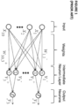
- Artificial neural networks mimic biological neural networks (the central nervous systems of animals, in particular the brain) and are used to estimate or approximate functions that can depend on a large number of inputs and are generally unknown. Artificial neural networks generally include layers of interconnected "neurons" which exchange messages between each other.
- the non-volatile memory arrays operate as an analog neuromorphic memory.
- the term neuromorphic means circuitry that implement models of neural systems.
- the analog neuromorphic memory includes a first plurality of synapses configured to receive a first plurality of inputs and to generate therefrom a first plurality of outputs, and a first plurality of neurons configured to receive the first plurality of outputs.
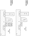
- each memory cell 210 includes source region 14 and drain region 16 formed in semiconductor substrate 12, with channel region 18 there between.
- Floating gate 20 is formed over and insulated from (and controls the conductivity of) a first portion of the channel region 18, and over a portion of the source region 14.
- Memory cell 210 is read by placing positive read voltages on the drain region 16 and word line terminal 22 (which turns on the portion of the channel region 18 under the word line terminal). If the floating gate 20 is positively charged (i.e. erased of electrons), then the portion of the channel region 18 under the floating gate 20 is turned on as well, and current will flow across the channel region 18, which is sensed as the erased or "1" state. If the floating gate 20 is negatively charged (i.e. programmed with electrons), then the portion of the channel region under the floating gate 20 is mostly or entirely turned off, and current will not flow (or there will be little flow) across the channel region 18, which is sensed as the programmed or "0" state.
- Figure 3 shows memory cell 310, which is similar to memory cell 210 of Figure 2 with the addition of control gate (CG) terminal 28.
- Control gate terminal 28 is biased at a high voltage, e.g., 10V, in programming, low or negative in erase, e.g., 0v/-8V, low or mid range in read, e.g., 0v/2.5V.
- Other terminals are biased similarly to that of Figure 2 .
- Figure 6 depicts a three-gate memory cell 610, which is another type of flash memory cell.
- Memory cell 610 is identical to the memory cell 410 of Figure 4 except that memory cell 610 does not have a separate control gate terminal.
- the erase operation (whereby erasing occurs through use of the erase gate terminal) and read operation are similar to that of the Figure 4 except there is no control gate bias applied.
- the programming operation also is done without the control gate bias, and as a result, a higher voltage must be applied on the source line terminal during a program operation to compensate for a lack of control gate bias.
- Table No. 5 depicts typical voltage ranges that can be applied to the terminals of memory cell 810 for performing read, erase, and program operations. In this Table, it is assumed that cell A (with terminals EG, CGA, and BLA) is selected for a read, program, or erase operation in each row Table No.
- the lines are configured so that each memory cell can be individually programmed, erased, and read without adversely affecting the memory state of other memory cells in the array, as further explained below.
- continuous (analog) programming of the memory cells is provided.
- the memory state (i.e. charge on the floating gate) of each memory cell in the array can be continuously changed from a fully erased state to a fully programmed state, independently and with minimal disturbance of other memory cells.
- the memory state (i.e., charge on the floating gate) of each memory cell in the array can be continuously changed from a fully programmed state to a fully erased state, and vice-versa, independently and with minimal disturbance of other memory cells.
- the cell storage is analog or at the very least can store one of many discrete values (such as 16 or 64 different values), which allows for very precise and individual tuning of all the cells in the memory array, and which makes the memory array ideal for storing and making fine tuning adjustments to the synapsis weights of the neural network.
- the methods and means described herein may apply to other non-volatile memory technologies such as FINFET split gate flash or stack gate flash memory, NAND flash, 3D flash, SONOS (silicon-oxide-nitride-oxide-silicon, charge trap in nitride), MONOS (metal-oxide-nitride-oxide-silicon, metal charge trap in nitride), ReRAM (resistive ram), PCM (phase change memory), MRAM (magnetic ram), FeRAM (ferroelectric ram), OTP (bi-level or multi-level one time programmable), and CeRAM (correlated electron ram), without limitation.
- the methods and means described herein may apply to volatile memory technologies used for neural network such as SRAM, DRAM, and other volatile synapse cells, without limitation.
- Figure 9 conceptually illustrates a non-limiting example of a neural network utilizing a non-volatile memory array of the present embodiments.
- This example uses the non-volatile memory array neural network for a facial recognition application, but any other appropriate application could be implemented using a non-volatile memory array based neural network.
- S0 is the input layer, which for this example is a 32x32 pixel RGB image with 5 bit precision (i.e. three 32x32 pixel arrays, one for each color R, G and B, each pixel being 5 bit precision).
- the synapses CB1 going from input layer S0 to layer C1 apply different sets of weights in some instances and shared weights in other instances, and scan the input image with 3x3 pixel overlapping filters (kernel), shifting the filter by 1 pixel (or more than 1 pixel as dictated by the model).
- values for 9 pixels in a 3x3 portion of the image are provided to the synapses CB1, where these 9 input values are multiplied by the appropriate weights and, after summing the outputs of that multiplication, a single output value is determined and provided by a first synapse of CB1 for generating a pixel of one of the layers of feature map C1.
- the 3x3 filter is then shifted one pixel to the right within input layer S0 (i.e., adding the column of three pixels on the right, and dropping the column of three pixels on the left), whereby the 9 pixel values in this newly positioned filter are provided to the synapses CB1, where they are multiplied by the same weights and a second single output value is determined by the associated synapse.
- This process is continued until the 3x3 filter scans across the entire 32x32 pixel image of input layer S0, for all three colors and for all bits (precision values).
- the process is then repeated using different sets of weights to generate a different feature map of C1, until all the features maps of layer C1 have been calculated.
- layer C1 in the present example, there are 16 feature maps, with 30x30 pixels each. Each pixel is a new feature pixel extracted from multiplying the inputs and kernel, and therefore each feature map is a two dimensional array, and thus in this example layer C1 constitutes 16 layers of two dimensional arrays (keeping in mind that the layers and arrays referenced herein are logical relationships, not necessarily physical relationships - i.e., the arrays are not necessarily oriented in physical two dimensional arrays). Each of the 16 feature maps in layer C1 is generated by one of sixteen different sets of synapse weights applied to the filter scans. The C1 feature maps could all be directed to different aspects of the same image feature, such as boundary identification.
- the first map (generated using a first weight set, shared for all scans used to generate this first map) could identify circular edges
- the second map generated using a second weight set different from the first weight set
- An activation function P1 (pooling) is applied before going from layer C1 to layer S1, which pools values from consecutive, non-overlapping 2x2 regions in each feature map.
- the purpose of the pooling function is to average out the nearby location (or a max function can also be used), to reduce the dependence of the edge location for example and to reduce the data size before going to the next stage.
- layer S1 there are 16 15x15 feature maps (i.e., sixteen different arrays of 15x15 pixels each).
- the synapses CB2 going from layer S1 to layer C2 scan maps in S1 with 4x4 filters, with a filter shift of 1 pixel.
- An activation function P2 (pooling) is applied before going from layer C2 to layer S2, which pools values from consecutive non-overlapping 2x2 regions in each feature map.
- layer S2 there are 22 6x6 feature maps.
- An activation function (pooling) is applied at the synapses CB3 going from layer S2 to layer C3, where every neuron in layer C3 connects to every map in layer S2 via a respective synapse of CB3.
- the synapses CB4 going from layer C3 to the output layer S3 fully connects C3 to S3, i.e. every neuron in layer C3 is connected to every neuron in layer S3.
- the output at S3 includes 10 neurons, where the highest output neuron determines the class. This output could, for example, be indicative of an identification or classification of the contents of the original image.
- Each layer of synapses is implemented using an array, or a portion of an array, of non-volatile memory cells.
- FIG 10 is a block diagram of a system that can be used for that purpose.
- VMM system 32 includes non-volatile memory cells and is utilized as the synapses (such as CB1, CB2, CB3, and CB4 in Figure 6 ) between one layer and the next layer.
- VMM system 32 comprises VMM array 33 comprising non-volatile memory cells arranged in rows and columns, erase gate and word line gate decoder 34, control gate decoder 35, bit line decoder 36 and source line decoder 37, which decode the respective inputs for the non-volatile memory cell array 33.
- Input to VMM array 33 can be from the erase gate and wordline gate decoder 34 or from the control gate decoder 35.
- Source line decoder 37 in this example also decodes the output of VMM array 33.
- bit line decoder 36 can decode the output of VMM array 33.
- VMM array 33 The output of VMM array 33 is supplied to a differential summer (such as a summing op-amp or a summing current mirror) 38, which sums up the outputs of VMM array 33 to create a single value for that convolution.
- the differential summer 38 is arranged to perform summation of both positive weight and negative weight inputs to output the single value.
- the input to VMM system 32 in Figure 10 can be analog level, binary level, digital timing pulses (in which case a pulses-to-analog converter PAC may be needed to convert pulses to the appropriate input analog level) or digital bits (in which case a DAC is provided to convert digital bits to appropriate input analog level) and the output can be analog level (e.g., current, voltage, or charge), binary level, digital pulses, or digital bits (in which case an output ADC is provided to convert output analog level into digital bits).
- analog level e.g., current, voltage, or charge
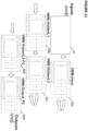
- FIG 11 is a block diagram depicting the usage of numerous layers of VMM systems 32, here labeled as VMM systems 32a, 32b, 32c, 32d, and 32e.
- the input denoted Inputx
- the converted analog inputs could be voltage or current.
- the input D/A conversion for the first layer could be done by using a function or a LUT (look up table) that maps the inputs Inputx to appropriate analog levels for the matrix multiplier of input VMM system 32a.
- the input conversion could also be done by an analog to analog (A/A) converter to convert an external analog input to a mapped analog input to the input VMM system 32a.
- the input conversion could also be done by a digital-to-digital pules (D/P) converter to convert an external digital input to a mapped digital pulse or pulses to the input VMM system 32a.
- A/A analog to analog
- D/P digital-to-digital pules
- the output generated by input VMM system 32a is provided as an input to the next VMM system (hidden level 1) 32b, which in turn generates an output that is provided as an input to the next VMM system (hidden level 2) 32c, and so on.
- the various layers of VMM system 32 function as different layers of synapses and neurons of a convolutional neural network (CNN).
- Each VMM system 32a, 32b, 32c, 32d, and 32e can be a stand-alone, physical system comprising a respective non-volatile memory array, or multiple VMM systems could utilize different portions of the same physical non-volatile memory array, or multiple VMM systems could utilize overlapping portions of the same physical non-volatile memory array.
- Each VMM system 32a, 32b, 32c, 32d, and 32e can also be time multiplexed for various portion of its array or neurons.
- the example shown in Figure 11 contains five layers (32a,32b,32c,32d,32e): one input layer (32a), two hidden layers (32b,32c), and two fully connected layers (32d,32e).
- layers 32a,32b,32c,32d,32e: one input layer (32a), two hidden layers (32b,32c), and two fully connected layers (32d,32e).
- One of ordinary skill in the art will appreciate that this is merely exemplary and that a system instead could comprise more than two hidden layers and more than two fully connected layers.
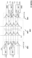
- FIG 12 depicts neuron VMM array 1200, which is particularly suited for memory cells 310 as shown in Figure 3 , and is utilized as the synapses and parts of neurons between an input layer and the next layer.
- VMM array 1200 comprises memory array 1201 of non-volatile memory cells and reference array 1202 (at the top of the array) of non-volatile reference memory cells. Alternatively, another reference array can be placed at the bottom.
- control gate lines such as control gate line 1203, run in a vertical direction (hence reference array 1202 in the row direction is orthogonal to control gate line 1203)
- erase gate lines such as erase gate line 1204, run in a horizontal direction.
- the inputs to VMM array 1200 are provided on the control gate lines (CGO, CG1, CG2, CG3), and the output of VMM array 1200 emerges on the source lines (SLO, SL1).
- SLO, SL1 source lines
- the current placed on each source line (SLO, SL1, respectively) performs a summing function of all the currents from the memory cells connected to that particular source line.
- the non-volatile memory cells of VMM array 1200 are preferably configured to operate in a sub-threshold region.
- Vg n * Vt * log Ids / wp * Io
- wp w of a reference or peripheral memory cell.
- wa W of each memory cell in the memory array.
- Vthp is the (equivalent or effective) threshold voltage of reference memory cell (or peripheral memory cell or transistor) and Vtha is the (equivalent or effective) threshold voltage of the array memory cell.
- a wordline or control gate can be used as the input for the memory cell for the input voltage.
- a memory cell such as a reference memory cell or a peripheral memory cell
- a transistor operating in the linear region or a resistor can be used to linearly convert an input/output current into an input/output voltage.
- FIG 14 depicts neuron VMM array 1400, which is particularly suited for memory cells 210 as shown in Figure 2 , and is utilized as the synapses and parts of neurons between an input layer and the next layer.
- VMM array 1400 comprises a memory array 1403 of non-volatile memory cells, reference array 1401 of first non-volatile reference memory cells, and reference array 1402 of second non-volatile reference memory cells. Reference arrays 1401 and 1402 run in row direction of the VMM array 1400.
- VMM array is similar to VMM 1300 except that in VMM array 1400, the word lines run in the vertical direction.
- FIG. 15 depicts neuron VMM array 1500, which is particularly suited for memory cells 310 as shown in Figure 3 , and is utilized as the synapses and parts of neurons between an input layer and the next layer.
- VMM array 1500 comprises a memory array 1503 of non-volatile memory cells, reference array 1501 of first non-volatile reference memory cells, and reference array 1502 of second non-volatile reference memory cells.
- Reference arrays 1501 and 1502 serve to convert current inputs flowing into terminals BLR0, BLR1, BLR2, and BLR3 into voltage inputs CG0, CG1, CG2, and CG3.
- an analog neural memory system comprises an array of non-volatile memory cells arranged into rows and columns, each non-volatile memory cell comprising a word line terminal, a bit line terminal, and an erase gate terminal; a plurality of word lines, each word line coupled to word line terminals of a row of non-volatile memory cells; a plurality of bit lines, each bit line coupled to bit line terminals of a column of non-volatile memory cells; and a plurality of erase gate lines, each erase gate line coupled to erase gate terminals of a page of non-volatile memory cells, the page comprising two words of non-volatile memory cells in adjacent rows.
- a method of performing tuning on a word or a page of non-volatile memory cells comprises erasing the word or page of non-volatile memory cells; performing soft programming of the word or page of non-volatile memory cells; performing coarse programing of the word or page of non-volatile memory cells; performing fine programming of the word or page of non-volatile memory cells; and identifying any fast bits in the word or page of non-volatile memory cells so that those bits can be programmed using a different sequence than the normal (non-fast and non-slow) bits.
- a method of programming a word of non-volatile memory cells in an array of non-volatile memory cells arranged into rows and columns, each non-volatile memory cell comprising a control gate terminal, a source line terminal and an erase gate terminal comprises ramping up a voltage on control gate terminals of the word of non-volatile memory cells to an intermediate voltage during a first time period; ramping up a voltage on the source line terminal of the word of non-volatile memory cells during a second time period after the first time period; ramping up a voltage on the erase gate line terminal of the word of non-volatile memory cells during a third time period after the second time period; and further ramping up the voltage on control gate terminals of the word of non-volatile memory cells during a fourth time period after the third time period.
- a method of programming a word of non-volatile memory cells in an array of non-volatile memory cells arranged into rows and columns, each non-volatile memory cell comprising a control gate terminal, a source line terminal and an erase gate terminal comprises ramping up a voltage on control gate terminals of the word of non-volatile memory cells to a first intermediate voltage during a first time period; ramping up a voltage on the source line terminal of the word of non-volatile memory cells to a second intermediate voltage during a second time period after the first time period; and ramping up a voltage on the erase gate line terminal of the word of non-volatile memory cells and further ramping up the voltage on the source line terminals of the word of non-volatile memory cells and further ramping up the voltage on the control gate terminals of the word of non-volatile memory cells to a third intermediate voltage during a third time period after the second time period; and further ramping up the voltage on control gate terminals of the word of non-volatile memory
- an analog neural memory system comprises an array of non-volatile memory cells arranged into rows and columns, each non-volatile memory cell comprising a word line terminal, a bit line terminal, and an erase gate terminal; a plurality of word lines, each word line coupled to word line terminals of a row of non-volatile memory cells; a plurality of bit lines, each bit line coupled to bit line terminals of a column of non-volatile memory cells; and a circuit decoder block comprising an erase gate decoder for providing an erase gate decoding signal, a control gate decoder for providing four control gate signals, and source line decoder that provides a source line decoding signal.
- an analog neural memory system comprises an array of non-volatile memory cells arranged into rows and columns, each non-volatile memory cell comprising a word line terminal, a bit line terminal, and an erase gate terminal; a plurality of word lines, each word line coupled to word line terminals of a row of non-volatile memory cells; a plurality of bit lines, each bit line coupled to bit line terminals of a column of non-volatile memory cells; and a circuit decoder block comprising an erase gate decoder for providing two erase gate decoding signals, a control gate decoder for providing eight control gate signals, and a source line decoder that provides a source line decoding signal.
- the artificial neural networks of the present invention utilize a combination of CMOS technology and non-volatile memory arrays.
- FIG. 17 depicts VMM array 1700.
- VMM array 1700 implements bi-directional tuning for a page of non-volatile memory cells.
- exemplary page 1701 comprises two words, each in a different row.
- a word includes a plurality of memory cells, e.g. 8-64.
- a special word may include just one cell or a few cells. Pairs of adjacent rows share a source line, such as SL0 or SL1. All cells in page 1701 share a common erase gate line that is controlled by erase gate enable transistor 1702, which controls the provision of a voltage to the erase gate terminals EGW of all cells in exemplary page set 1701.
- all cells in page 1701 can be erased at the same time.
- cells in page 1701 can be bi-directionally tuned through program and erase operations and some cells in page 1701 can be uni-directionally tuned through program operation.
- the program operations can include the precision programming techniques described below with reference to Figures 20 and 21 . If too much electron charge is placed on a floating gate (which would cause an incorrect current value to be stored in the cell, i.e. a current value lower than the intended current value), the cell must be erased and the sequence of partial programming operations must start over.
- FIG. 18 depicts VMM array 1800.
- VMM array 1800 implements bi-directional tuning for a word of non-volatile memory cells.
- exemplary word 1801 comprises a plurality of cells in a row. All cells in word 1801 share a common erase gate line that is controlled by erase gate enable transistor 1802, which controls the provision of a voltage to the erase gate terminals of all cells in word 1801.
- all cells in word 1801 can be erased at the same time.
- cells in word 1801 can be bi-directionally tuned through program and erase operations.
- the program operations can include the precision programming techniques described below. If too much electron charge is placed on a floating gate (such that an incorrect current value is stored in the cell, i.e. a current value lower than the intended current value), the cell must be erased and the sequence of partial programming operations must start over.
- FIG. 19 depicts VMM array 1900.
- VMM array 1900 implements bi-directional tuning for a word of non-volatile memory cells.
- exemplary word 1901 comprises two half words of cells. Each half word belongs to a row that shares an erase gate. All cells in word 1901 share a common erase gate line connected to erase gate terminal EGW. Unlike in VMM array 1800 and 1700, there is no erase gate enable transistor. Here, all cells in word 1901 can be erased at the same time. Thereafter, cells in word 1901 can be bi-directionally tuned through program and erase operations.
- the program operations can include the precision programming techniques described below. If too much electron charge is placed on a floating gate (such that an incorrect current value is stored in the cell, i.e. a current value lower than the intended current value), the cell must be erased and the sequence of partial programming operations must start over.
- source line pulldown bitlines can be used, as described in U.S. Provisional Patent Application No. 62/981,757 filed on February 26, 2020, and titled, "Ultra-Precise Tuning of Analog Neural Memory Cells In A Deep Learning Artificial Neural Network,” which is incorporated by reference herein.
- FIG 20A depicts tuning page/word algorithm 2000, which can be applied to VMM arrays 1700, 1800, or 1900 in Figures 17-19 .
- the word or page is erased (step 2001).
- deep programming is performed on the un-used cells (step 2002). Deep programming is used to program the cells into a state (or target level) that has insignificant cell current during a read operation, for example ⁇ pA range.
- coarse programming is performed on the cells within the word or page (step 2003). Coarse programming is used to program the cells into a coarse target level, for example within 50-500% of the target with large (coarse) increment voltage and/or program current and/or program timing.
- fine programming is performed on the cells within the word or page (step 2004).
- FIG 20B depicts tuning page/word algorithm 2050, which can be applied to VMM arrays 1700, 1800, or 1900 in Figures 17-19 .
- Tuning page/word algorithm 2050 is similar to tuning/page word algorithm 2000 in Figure 20A , except that tuning page/word algorithm 2050 further includes steps for handling fast or slow bits. Steps 2001-2005 occur as in Figure 20A .
- step 2006 or alternatively in step 2003 a determination is made whether the word or page contains any fast-bits or slow-bits (step 2006).
- a fast bit is a bit that requires a shorter period of programming to reach a desired level than a normal bit
- a slow bit is a bit that requires a longer period of programming to reach a desired level than a normal bit.
- the slow bit can be detected by monitoring the program rate delta Ir/ delta tprog ⁇ a pre-determined R factor. If no, then the algorithm stops. If yes, then the fast-bit or slow-bit cells are identified and flagged. Thereafter, any programming of that word or page will utilize fastbit or slowbit algorithms, as discussed below with reference to Figures 21A and 21B .
- FIG 21A depicts fast-bit algorithm 2100. This is performed if a word or page has been determined to contain one or more fast-bit cells, also known as fast-bits.
- the word or page is erased or partially erased (step 2101).
- the fast-bits are programmed and verified (step 2102). This is for example done with smaller than the default (or constant) voltage increment and/or smaller than the default program current and/or smaller than the default timing.
- the normal bits i.e. all bits not flagged as fast-bits or slow-bits, are programmed and verified (step 2103). This is for example done with default setting of coarse/fine/ultrafine voltage increment and/or program current and/or timing
- Figure 21B depicts slowbit algorithm 2150.
- step 2151 the word or page is erased or partially erase.
- step 2152 the slow-bit cells are programmed and verified. This is for example done with larger than the default voltage increment and/or larger than the default program current and/or larger than the default timing.
- step 2153 the normal bits, i.e. all bits not flagged as slow-bits or fast-bits, are programmed and verified. This is for example done with default setting of coarse/fine/ultrafine voltage increment and/or program current and/or timing
- the slow-bit cells are tuned first to avoid disturb to other cells in the same page/word, then fast-bit cells are tuned, and then normal-bit cells are tuned.
- the slow-bit cells are tuned first (to avoid disturb to other cells in the same page/word), then normal-bit cells are tuned, and then fast-bit cells are tuned.
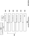
- FIG. 22 depicts a block diagram of VMM system 2200.
- VMM system 2200 comprises VMM array 2201, row decoders 2202, high voltage decoders 2203, column decoders 2204, bit line drivers 2205, input circuit 2206, output circuit 2207, control logic 2208, and bias generator 2209.
- VMM system 2200 further comprises high voltage generation block 2210, which comprises charge pump 2211, charge pump regulator 2212, and high voltage level generator 2213.
- VMM system 2200 further comprises (program/erase, or aka weight tuning) algorithm controller 2214, analog circuitry 2215, control logic 2216, and test control logic 2217. The systems and methods described below can be implemented in VMM system 2200.
- the output circuit 2207 may include circuits such as a ADC (analog to digital converter, to convert neuron analog output to digital bits), AAC (analog to analog converter, such as a current to voltage converter), APC (analog to pulse(s) converter), or any other type of converters.
- the output circuit 2207 may implement an activation function such as ReLU or sigmoids.
- the output circuit 2207 may implement statistic normalization, regularization, up/down scaling functions, statistical rounding, or arithmetic functions (e.g., add, subtract, divide, multiply, shift, log) for neuron outputs.
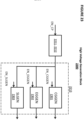
- FIG. 23 depicts high voltage generation block 2300, which is an embodiment of high voltage generation block 2210 from Figure 22 .
- High voltage generation block 2300 comprises charge pump 2211 and charge pump regulator 2212, which generate a variety of high voltages and are controlled by an enable signal here labeled as EN_CP.
- Charge pump 2211 and charge pump regulator 2212 provide the requisite high voltages to control gate high voltage generator 2301, erase gate high voltage generator 2302, and source line high voltage generator 2303, which are controlled by enable signals labeled EN_CGGEN, EN_EGGEN, and EN_SLGEN, respectively, and which provide high voltage signals to control gate lines, erase gate lines, and source lines, respectively, as needed during program, erase, or read operations within a VMM array.
- Figure 24 depicts a high voltage maximum circuit, used to supply the high voltage power supply, which identifies the voltage that is highest between a first high voltage HV1 and a second high voltage HV2 and outputs the highest voltage.
- Comparator 2401 receives HV1div and HV2div, which are level-shifted, divided down (i.e. low voltage) versions of HV1 and HV2, respectively.
- Comparator 2401 outputs a high signal on line COMPO if HV1 is greater than HV2, and it outputs a low signal on line COMPO if HV1 is less than HV2.
- the output of comparator 2401 on line COMPO is provided to high voltage level shifter 2402 and high voltage level shifter 2403.
- PMOS transistors 2404, 2405, 2406, and 2407 are configured as shown, i.e. with their gate coupled to a respective one of lines 2402A, 2402B, 2403A and 2403B.
- high voltage output 2408 will be equivalent to HV2, less any voltage drop across PMOS transistors 2406, 2407. If high voltage level shifter 2402 outputs a low signal on the line 2402A and high voltage level shifter 2403 outputs a low signal on the line 2403B, then high voltage output 2408 will be equivalent to HV1, less any voltage drop across PMOS transistors 2404, 2405.
- FIG. 25 depicts high voltage generation block 2500, which is another embodiment of high voltage generation block 2412.
- high voltage generation block 2500 comprises charge pump and regulator 2501 enabled by signal EN_CP, high voltage increment reference generator 2503, and high voltage buffer operational amplifier 2502.
- the voltage of the output of charge pump regulator 2503 can be controlled based on the signals sent to the gates of the MOS transistors in high voltage increment reference generator 2503, by trimming the portion of the output voltage HVSUP output by charge pump 2501 fed to the input of high voltage op-amp HVOPA.
- FIG. 26 depicts high voltage generator block 2600, which is another embodiment of high voltage generation block 2412.
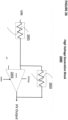
- High voltage generation block 2600 receives input VIN (a low voltage signal) and generates output HV Output (a high voltage signal), and comprises operational amplifier 2603, variable resistor 2601, and variable resistor 2602, where the gain (of operational amplifier 2601 is dependent on the values of variable resistor 2601 and/or variable resistor 2602.
- the high voltage increment value is hence controlled by the value of the variable resistor 2601 and/or resistor 2602.
- Figure 27A depicts ramp down control circuit 2700, which comprises clamp PMOS transistor 2701, enabling NMOS transistor 2702, and current bias NMOS transistor 2703, configured as shown.
- Ramp down circuit 2700 receives voltage HV to be ramped down at the source of PMOS transistor 2701 and generates output signal VHV_DET at the drain of PMOS transistor 2701, which will have a peak value of HV and will ramp down toward ground in response to signal ENRMP, fed to the gate of enabling NMOS transistor 2702, changing from low to high.
- Output signal VHV_DET will be ramped down from HV value to Vcas+Vt PH value by a current controlled by the current bias NMOS transistor 2703 when ENRMP equals to high.
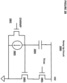
- Figure 28 depicts ramp up circuit 2800, which comprises NMOS cascoding transistor 2801, enabling NMOS transistor 2802, current shunt NMOS transistor 2803, current source 2805, and capacitor 2804, configured as shown.
- the ramp rate on the HV node is such that the current injected through the capacitor 2804 is equal to the current source 2805.
- Figures 29A, 29B, and 29C depict VMM high voltage decode circuits, comprising word line decoder circuit 2901, source line decoder circuit 2904, and high voltage level shifter 2908, which are appropriate for use with memory cells of the type shown in Figure 2 .
- source line decoder circuit 2904 comprises NMOS monitor transistors 2905 (controlled by signal HVO), driving transistor 2906 (controlled by signal HVO), and de-select transistor 2907 (controlled by signal HVO_B), configured as shown.
- signal HV0 is high
- the voltage appearing on line SLSUP is passed through to line SL, and appears on monitoring line SL_MON.
- signal HVO_B is high, line SL is pulled down.
- high voltage level shifter 2908 receives enable signal EN and outputs high voltage signal HV0 and its complement HVO_B between HVSUP, e.g., 12V, and HVSUP_LOW supply, e.g., 0V (when HVSUP is for example equal to an intermediate level ⁇ 5V) or 2.5V (when HVSUP is for example 12V).
- HV0 can be 5V and HVO_B can be 0V, or HVO can be 12V and HVO_B can be 2.5V
- FIGS 30A-30D depict VMM high voltage decode circuits, comprising erase gate decoder circuit 3001, control gate decoder circuit 3004, source line decoder circuit 3007, and high voltage level shifter 3011, which are appropriate for use with memory cells of the type shown in Figure 3 .
- erase gate decoder circuit 3001 and control gate decoder circuit 3004 use the same design as word line decoder circuit 2901 in Figure 29A .
- source line decoder circuit 3007 uses the same design as source line decoder circuit 2904 in Figure 29 .
- high voltage level shifter 3011 uses the same design as high voltage level shifter 2908 in Figure 29 .
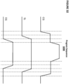
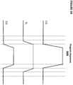
- Figures 31-34 depict programming sequences of voltages applied to a control gate terminal, source line terminal, and erase gate terminal of one or more non-volatile memory cells during a program operation.
- Figure 31 depicts program sequence 3100, where the control gate voltage CG ramps up during a first period, then the source line voltage SL ramps up during a second period, and then the erase gate voltage EG ramps up during a third period. All three voltages plateau at their peak values during a fourth period, and then the ramping sequence is reversed, erase gate voltage EG ramps down during a fifth period, source line voltage SL ramps down during a sixth period, and control gate voltage CG ramps down during a seventh period.
- Program sequence 3100 minimizes erase gate disturb occurrences.
- Figure 32 depicts program sequence 3200, where the control gate voltage CG ramps up during a first period to an intermediate value, then the source line voltage SL ramps up during a second period to its peak value, and then the erase gate voltage EG ramps up to a third period to its peak value, and then the control gate voltage CG ramps up during a fourth period to its peak value. All three voltages plateau at their peak values during a fifth period, and then control gate voltage CG ramps down during a sixth period to an intermediate value, erase gate voltage EG ramps down during a seventh period, source line voltage SL ramps down during an eighth period, and control gate voltage CG then ramps down to ground during a ninth period.
- Figure 33 depicts program sequence 3300, where first the control gate voltage CG ramps up to a first intermediate value during a first period and then during a second period the source line voltage SL ramps up to a second intermediate value. Then, during a third period, the control gate voltage CG ramps up to a third intermediate value while the source line voltage SL ramps up to its peak voltage and the erase gate voltage EG ramps to its peak voltage. Finally, during a fourth period, the control gate voltage CG ramps up to its peak voltage. Then all three voltages plateau at their peak values during a fifth period.
- control gate voltage CG ramps down to the third intermediate value
- the source line voltage SL ramps down to the second intermediate value
- the control gate voltage CG ramps down to the first intermediate value
- the erase gate voltage EG ramps down to ground
- the source line voltage SL ramps down to ground
- the control gate voltage CG ramps down to ground.
- Figure 34 depicts program sequence 3400, where the source line voltage SL ramps up during a first period to a peak value, and then during a second period the control gate line voltage CG ramps up to its peak value while the erase gate voltage EG ramps up to its peak value. Then during a third period all three voltages plateau at their peak values. Then the control gate line voltage CG ramps down during a fourth period while the erase gate voltage EG ramps down, and then during a fifth period the source line voltage SL ramps down. Program sequence 3400 minimizes control gate disturb occurrences.
- Figure 35 depicts erase sequence 3500, where the inhibit control gate or inhibit source line (CG-inh or SL-inh, to be applies to unselected cells during an operation) ramps up during a first period, and then erase gate voltage EG ramps up during a second period. Then all voltage plateau at their peak values during a third period. Then the erase gate voltage EG ramp down during a fourth period, and then the inhibit control gate or inhibit source line (CG-inh or SL-inh) ramps down during a fifth period.
- This sequence is for example suitable for arrays that are suitable for bi-directional tuning such as Figure 12 , 14 , 16 , 19 .
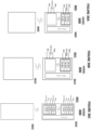
- Figures 36A, 36B, and 36C depict a high voltage decoder 3600 that utilizes the decoding sub circuit blocks 3001 (EG dec), 3004 (CG dec), 3007 (SL dec) in Figure 30 .
- Different arrangement of sub circuit blocks are done as shown to optimize for different configurations and optimizations.
- Figure 36A shows circuit decoder block 3601 that comprises circuit decoder block 3602.
- the circuit decoder block 3602 includes EG dec that provides one EG decoding signal, CG dec that provides two CG decoding signals, and SL dec that provides one SL decoding signal.
- Figure 36B shows circuit decoder block 3611 that comprises circuit decoder block 3612.
- the circuit decoder block 3612 includes EG dec that provides one EG decoding signal, CG dec that provides four CG decoding signals, and SL dec that provides one SL decoding signal.
- Figure 36C shows circuit decoder block 3621 that comprises circuit decoder block 3622.
- the circuit decoder block 3622 t includes EG dec that provides two EG decoding signals, CG dec that provides eight CG decoding signals, and SL dec that provides one SL decoding signal.
- High voltage latch circuit 3700 comprises a cross coupled high voltage transistor inverter formed by PMOS transistors 3711 and 3712 and NMOS transistors 3713 and 3714 and enabling transistors 3715 and 3716.
- Output HVOUT 3704 and complementary signal HVOUTB 3703 are generated.
- adjacent includes “directly adjacent” (no intermediate materials, elements or space disposed therebetween) and “indirectly adjacent” (intermediate materials, elements or space disposed there between)
- mounted to includes “directly mounted to” (no intermediate materials, elements or space disposed there between) and “indirectly mounted to” (intermediate materials, elements or spaced disposed there between)
- electrically coupled includes “directly electrically coupled to” (no intermediate materials or elements there between that electrically connect the elements together) and “indirectly electrically coupled to” (intermediate materials or elements there between that electrically connect the elements together).
- forming an element "over a substrate” can include forming the element directly on the substrate with no intermediate materials/elements therebetween, as well as forming the element indirectly on the substrate with one or more intermediate materials/elements there between. Further examples of the invention are given below:
Landscapes
- Engineering & Computer Science (AREA)
- Microelectronics & Electronic Packaging (AREA)
- Health & Medical Sciences (AREA)
- Life Sciences & Earth Sciences (AREA)
- Biomedical Technology (AREA)
- Physics & Mathematics (AREA)
- Molecular Biology (AREA)
- General Health & Medical Sciences (AREA)
- Neurology (AREA)
- Biophysics (AREA)
- Theoretical Computer Science (AREA)
- Computer Hardware Design (AREA)
- Mathematical Physics (AREA)
- Computing Systems (AREA)
- General Engineering & Computer Science (AREA)
- General Physics & Mathematics (AREA)
- Evolutionary Computation (AREA)
- Software Systems (AREA)
- Computational Linguistics (AREA)
- Artificial Intelligence (AREA)
- Data Mining & Analysis (AREA)
- Non-Volatile Memory (AREA)
- Read Only Memory (AREA)
- Semiconductor Memories (AREA)
Applications Claiming Priority (4)
| Application Number | Priority Date | Filing Date | Title |
|---|---|---|---|
| US202062993008P | 2020-03-22 | 2020-03-22 | |
| US17/024,410 US11532354B2 (en) | 2020-03-22 | 2020-09-17 | Precision tuning of a page or word of non-volatile memory cells and associated high voltage circuits for an analog neural memory array in an artificial neural network |
| EP20786400.0A EP4128239B1 (de) | 2020-03-22 | 2020-09-22 | Verfahren zur programmierung eines wortes von nichtflüchtigen speicherzellen in einer anordnung von nichtflüchtigen speicherzellen |
| PCT/US2020/052068 WO2021194547A1 (en) | 2020-03-22 | 2020-09-22 | Precision tuning of a page or word of non-volatile memory cells and associated high voltage circuits for an analog neural memory array in an artificial neural network |
Related Parent Applications (2)
| Application Number | Title | Priority Date | Filing Date |
|---|---|---|---|
| EP20786400.0A Division-Into EP4128239B1 (de) | 2020-03-22 | 2020-09-22 | Verfahren zur programmierung eines wortes von nichtflüchtigen speicherzellen in einer anordnung von nichtflüchtigen speicherzellen |
| EP20786400.0A Division EP4128239B1 (de) | 2020-03-22 | 2020-09-22 | Verfahren zur programmierung eines wortes von nichtflüchtigen speicherzellen in einer anordnung von nichtflüchtigen speicherzellen |
Publications (2)
| Publication Number | Publication Date |
|---|---|
| EP4553707A2 true EP4553707A2 (de) | 2025-05-14 |
| EP4553707A3 EP4553707A3 (de) | 2025-08-06 |
Family
ID=77748196
Family Applications (2)
| Application Number | Title | Priority Date | Filing Date |
|---|---|---|---|
| EP25166190.6A Pending EP4553707A3 (de) | 2020-03-22 | 2020-09-22 | Verfahren zur programmierung eines wortes nichtflüchtiger speicherzellen in einem array nichtflüchtiger speicherzellen |
| EP20786400.0A Active EP4128239B1 (de) | 2020-03-22 | 2020-09-22 | Verfahren zur programmierung eines wortes von nichtflüchtigen speicherzellen in einer anordnung von nichtflüchtigen speicherzellen |
Family Applications After (1)
| Application Number | Title | Priority Date | Filing Date |
|---|---|---|---|
| EP20786400.0A Active EP4128239B1 (de) | 2020-03-22 | 2020-09-22 | Verfahren zur programmierung eines wortes von nichtflüchtigen speicherzellen in einer anordnung von nichtflüchtigen speicherzellen |
Country Status (7)
| Country | Link |
|---|---|
| US (4) | US11532354B2 (de) |
| EP (2) | EP4553707A3 (de) |
| JP (2) | JP7561203B2 (de) |
| KR (2) | KR20250093581A (de) |
| CN (1) | CN115298738A (de) |
| TW (2) | TW202422559A (de) |
| WO (1) | WO2021194547A1 (de) |
Families Citing this family (6)
| Publication number | Priority date | Publication date | Assignee | Title |
|---|---|---|---|---|
| US11755899B2 (en) * | 2019-11-11 | 2023-09-12 | Silicon Storage Technology, Inc. | Precise programming method and apparatus for analog neural memory in an artificial neural network |
| KR102582419B1 (ko) * | 2021-08-04 | 2023-09-26 | 한국과학기술원 | 인 메모리 컴퓨팅을 통해 컨벌루션 뉴럴 네트워크 연산을 수행하는 방법 |
| CN114597232B (zh) * | 2022-05-10 | 2022-07-19 | 华中科技大学 | 一种实现负权重的矩阵乘和运算的crossbar器件制备方法 |
| US12243587B2 (en) * | 2022-09-22 | 2025-03-04 | Silicon Storage Technology, Inc. | Multiple row programming operation in artificial neural network array |
| KR102885729B1 (ko) * | 2023-03-31 | 2025-11-13 | 서울대학교산학협력단 | 업데이트 셀과 이를 포함하는 뉴로모픽 회로 및 뉴로모픽 회로의 동작 방법 |
| TWI900324B (zh) * | 2024-11-08 | 2025-10-01 | 旺宏電子股份有限公司 | 記憶體裝置的操作方法 |
Citations (3)
| Publication number | Priority date | Publication date | Assignee | Title |
|---|---|---|---|---|
| US5029130A (en) | 1990-01-22 | 1991-07-02 | Silicon Storage Technology, Inc. | Single transistor non-valatile electrically alterable semiconductor memory device |
| US6747310B2 (en) | 2002-10-07 | 2004-06-08 | Actrans System Inc. | Flash memory cells with separated self-aligned select and erase gates, and process of fabrication |
| US20170337466A1 (en) | 2016-05-17 | 2017-11-23 | Silicon Storage Technology, Inc. | Deep Learning Neural Network Classifier Using Non-volatile Memory Array |
Family Cites Families (43)
| Publication number | Priority date | Publication date | Assignee | Title |
|---|---|---|---|---|
| US5353382A (en) * | 1990-10-15 | 1994-10-04 | California Institute Of Technology | Programmable synapse for neural network applications |
| US5657332A (en) * | 1992-05-20 | 1997-08-12 | Sandisk Corporation | Soft errors handling in EEPROM devices |
| US5336937A (en) * | 1992-08-28 | 1994-08-09 | State University Of New York | Programmable analog synapse and neural networks incorporating same |
| US6160739A (en) * | 1999-04-16 | 2000-12-12 | Sandisk Corporation | Non-volatile memories with improved endurance and extended lifetime |
| US6643185B1 (en) | 2002-08-07 | 2003-11-04 | Advanced Micro Devices, Inc. | Method for repairing over-erasure of fast bits on floating gate memory devices |
| GB2395065B (en) * | 2002-10-30 | 2005-01-19 | Toumaz Technology Ltd | Floating gate transistors |
| JP2005235287A (ja) * | 2004-02-19 | 2005-09-02 | Nec Electronics Corp | 不揮発性半導体記憶装置のプログラミング方法、プログラミング装置、及び、不揮発性半導体記憶装置 |
| US7173859B2 (en) | 2004-11-16 | 2007-02-06 | Sandisk Corporation | Faster programming of higher level states in multi-level cell flash memory |
| WO2007050976A1 (en) | 2005-10-27 | 2007-05-03 | Sandisk Corporation | Method for programming of multi-state non-volatile memory using smart verify |
| JP4435200B2 (ja) * | 2007-04-03 | 2010-03-17 | 株式会社東芝 | 半導体記憶装置のデータ書き込み方法 |
| US7768836B2 (en) | 2008-10-10 | 2010-08-03 | Sandisk Corporation | Nonvolatile memory and method with reduced program verify by ignoring fastest and/or slowest programming bits |
| US8174895B2 (en) | 2009-12-15 | 2012-05-08 | Sandisk Technologies Inc. | Programming non-volatile storage with fast bit detection and verify skip |
| KR101691094B1 (ko) * | 2010-08-09 | 2016-12-30 | 삼성전자주식회사 | 불휘발성 메모리 장치 및 그것을 포함하는 메모리 시스템 |
| TW201230045A (en) * | 2011-01-06 | 2012-07-16 | Macronix Int Co Ltd | Method for increasing program speed and control read windows for multi-level cell non-volatile memory |
| US8842476B2 (en) * | 2011-11-09 | 2014-09-23 | Sandisk Technologies Inc. | Erratic program detection for non-volatile storage |
| US8804429B2 (en) * | 2011-12-08 | 2014-08-12 | Silicon Storage Technology, Inc. | Non-volatile memory device and a method of programming such device |
| JP2013143155A (ja) | 2012-01-06 | 2013-07-22 | Powerchip Technology Corp | 不揮発性半導体記憶装置とその書き込み方法 |
| US9430735B1 (en) * | 2012-02-23 | 2016-08-30 | Micron Technology, Inc. | Neural network in a memory device |
| KR20130098643A (ko) * | 2012-02-28 | 2013-09-05 | 삼성전자주식회사 | 불휘발성 메모리 장치 및 그것을 포함하는 임베디드 메모리 시스템 |
| KR102083271B1 (ko) | 2012-07-31 | 2020-03-02 | 삼성전자주식회사 | 플래시 메모리의 물리적 특성을 이용하여 난수를 생성하는 플래시 메모리 시스템 및 그것의 난수 생성 방법 |
| KR102012903B1 (ko) * | 2012-10-30 | 2019-08-21 | 삼성전자주식회사 | 불휘발성 메모리 장치 및 불휘발성 메모리 장치의 프로그램 방법 |
| KR102137075B1 (ko) * | 2013-09-10 | 2020-07-23 | 에스케이하이닉스 주식회사 | 반도체 메모리 장치 및 그 프로그램 방법 |
| US9418744B2 (en) * | 2014-05-12 | 2016-08-16 | Silicon Storage Technology, Inc. | System and method to reduce disturbances during programming of flash memory cells |
| US9361995B1 (en) | 2015-01-21 | 2016-06-07 | Silicon Storage Technology, Inc. | Flash memory system using complementary voltage supplies |
| US11055606B2 (en) * | 2016-03-21 | 2021-07-06 | HangZhou HaiCun Information Technology Co., Ltd. | Vertically integrated neuro-processor |
| EP3459019B1 (de) * | 2016-05-17 | 2025-09-17 | Silicon Storage Technology, Inc. | Tiefenlernender neuronaler netzwerkklassifizierer mit nichtflüchtiger speicheranordnung |
| US9953719B2 (en) * | 2016-05-18 | 2018-04-24 | Silicon Storage Technology, Inc. | Flash memory cell and associated decoders |
| US10026486B1 (en) * | 2017-03-06 | 2018-07-17 | Sandisk Technologies Llc | First read countermeasures in memory |
| US11087207B2 (en) * | 2018-03-14 | 2021-08-10 | Silicon Storage Technology, Inc. | Decoders for analog neural memory in deep learning artificial neural network |
| US11361215B2 (en) * | 2017-11-29 | 2022-06-14 | Anaflash Inc. | Neural network circuits having non-volatile synapse arrays |
| US10748630B2 (en) | 2017-11-29 | 2020-08-18 | Silicon Storage Technology, Inc. | High precision and highly efficient tuning mechanisms and algorithms for analog neuromorphic memory in artificial neural networks |
| US10552510B2 (en) * | 2018-01-11 | 2020-02-04 | Mentium Technologies Inc. | Vector-by-matrix multiplier modules based on non-volatile 2D and 3D memory arrays |
| US10910061B2 (en) * | 2018-03-14 | 2021-02-02 | Silicon Storage Technology, Inc. | Method and apparatus for programming analog neural memory in a deep learning artificial neural network |
| US10559353B2 (en) * | 2018-06-06 | 2020-02-11 | Micron Technology, Inc. | Weight storage using memory device |
| US10692570B2 (en) * | 2018-07-11 | 2020-06-23 | Sandisk Technologies Llc | Neural network matrix multiplication in memory cells |
| US11328204B2 (en) * | 2018-07-24 | 2022-05-10 | Sandisk Technologies Llc | Realization of binary neural networks in NAND memory arrays |
| US12217808B2 (en) | 2018-11-18 | 2025-02-04 | NEO Semiconductor, Inc. | Methods and apparatus for NAND flash memory |
| US11270763B2 (en) * | 2019-01-18 | 2022-03-08 | Silicon Storage Technology, Inc. | Neural network classifier using array of three-gate non-volatile memory cells |
| KR102786592B1 (ko) * | 2019-07-01 | 2025-03-27 | 삼성전자주식회사 | 불휘발성 메모리 장치 및 이의 동작 방법 |
| US20210193671A1 (en) * | 2019-12-20 | 2021-06-24 | Silicon Storage Technology, Inc. | Method Of Forming A Device With Split Gate Non-volatile Memory Cells, HV Devices Having Planar Channel Regions And FINFET Logic Devices |
| US11636322B2 (en) * | 2020-01-03 | 2023-04-25 | Silicon Storage Technology, Inc. | Precise data tuning method and apparatus for analog neural memory in an artificial neural network |
| US11393535B2 (en) | 2020-02-26 | 2022-07-19 | Silicon Storage Technology, Inc. | Ultra-precise tuning of analog neural memory cells in a deep learning artificial neural network |
| US11355184B2 (en) * | 2020-03-05 | 2022-06-07 | Silicon Storage Technology, Inc. | Analog neural memory array in artificial neural network with substantially constant array source impedance with adaptive weight mapping and distributed power |
-
2020
- 2020-09-17 US US17/024,410 patent/US11532354B2/en active Active
- 2020-09-22 KR KR1020257020069A patent/KR20250093581A/ko active Pending
- 2020-09-22 CN CN202080098758.7A patent/CN115298738A/zh active Pending
- 2020-09-22 WO PCT/US2020/052068 patent/WO2021194547A1/en not_active Ceased
- 2020-09-22 JP JP2022556563A patent/JP7561203B2/ja active Active
- 2020-09-22 KR KR1020227031891A patent/KR102823670B1/ko active Active
- 2020-09-22 EP EP25166190.6A patent/EP4553707A3/de active Pending
- 2020-09-22 EP EP20786400.0A patent/EP4128239B1/de active Active
-
2021
- 2021-03-12 TW TW113103871A patent/TW202422559A/zh unknown
- 2021-03-12 TW TW110108871A patent/TWI834955B/zh active
-
2022
- 2022-07-01 US US17/856,839 patent/US11915747B2/en active Active
- 2022-07-04 US US17/857,113 patent/US11798619B2/en active Active
-
2024
- 2024-01-22 US US18/419,079 patent/US20240312517A1/en active Pending
- 2024-09-20 JP JP2024163480A patent/JP2025011108A/ja active Pending
Patent Citations (3)
| Publication number | Priority date | Publication date | Assignee | Title |
|---|---|---|---|---|
| US5029130A (en) | 1990-01-22 | 1991-07-02 | Silicon Storage Technology, Inc. | Single transistor non-valatile electrically alterable semiconductor memory device |
| US6747310B2 (en) | 2002-10-07 | 2004-06-08 | Actrans System Inc. | Flash memory cells with separated self-aligned select and erase gates, and process of fabrication |
| US20170337466A1 (en) | 2016-05-17 | 2017-11-23 | Silicon Storage Technology, Inc. | Deep Learning Neural Network Classifier Using Non-volatile Memory Array |
Also Published As
| Publication number | Publication date |
|---|---|
| TWI834955B (zh) | 2024-03-11 |
| KR20250093581A (ko) | 2025-06-24 |
| WO2021194547A1 (en) | 2021-09-30 |
| TW202141502A (zh) | 2021-11-01 |
| KR20220141855A (ko) | 2022-10-20 |
| CN115298738A (zh) | 2022-11-04 |
| US11798619B2 (en) | 2023-10-24 |
| TW202422559A (zh) | 2024-06-01 |
| JP7561203B2 (ja) | 2024-10-03 |
| US20210295907A1 (en) | 2021-09-23 |
| US20220336010A1 (en) | 2022-10-20 |
| KR102823670B1 (ko) | 2025-06-27 |
| EP4128239A1 (de) | 2023-02-08 |
| EP4128239B1 (de) | 2025-06-11 |
| JP2025011108A (ja) | 2025-01-23 |
| US11532354B2 (en) | 2022-12-20 |
| JP2023518469A (ja) | 2023-05-01 |
| US20240312517A1 (en) | 2024-09-19 |
| EP4553707A3 (de) | 2025-08-06 |
| US11915747B2 (en) | 2024-02-27 |
| US20220336011A1 (en) | 2022-10-20 |
Similar Documents
| Publication | Publication Date | Title |
|---|---|---|
| EP3963512B1 (de) | Dekodierungssystem und physikalisches layout für analogen neuronalen speicher in einem tief lernenden künstlichen neuronalen netz | |
| EP4407874B1 (de) | Verfahren zum betrieb eines analogen neuronalen speichersystems | |
| EP3844680B1 (de) | Temperatur- und leckagekompensation für speicherzellen in einem analogen neuronalen speichersystem, das in einem tiefen lernenden neuronalen netzwerk verwendet wird | |
| EP4128239B1 (de) | Verfahren zur programmierung eines wortes von nichtflüchtigen speicherzellen in einer anordnung von nichtflüchtigen speicherzellen | |
| EP4205116B1 (de) | Gleichzeitige schreib- und verifizierungsoperationen in einem analogen neuronalen speicher | |
| EP4141875A1 (de) | Verfahren und vorrichtung zum vergleichen eines stromes einer ausgewählten zelle | |
| EP4162491B1 (de) | Wortleitungs- und steuergateleitungs-tandemdecodierer für analogen neuronalen speicher in einem künstlichen neuronalen tiefenlernnetz | |
| US20260031112A1 (en) | Bitline regulation circuit | |
| EP4381504B1 (de) | Ausgangsschaltung für analogen neuronalen speicher in einem künstlichen neuronalen tiefenlernnetz | |
| EP4341934B1 (de) | Geteilte arrayarchitektur für analogen neuronalen speicher in einem künstlichen neuronalen tiefenlernnetz | |
| US20220374696A1 (en) | Split array architecture for analog neural memory in a deep learning artificial neural network | |
| US12469523B2 (en) | Current-to-voltage converter comprising common mode circuit | |
| US20240256846A1 (en) | Multiplexors for neural network array | |
| EP4385016B1 (de) | Hybrides speichersystem, das zur speicherung von gewichtsdaten eines neuronalen speichers in analoger oder digitaler form konfiguriert werden kann | |
| EP4469940B1 (de) | Künstliches neuronales netzwerk mit einem analogen array und einem digitalen array | |
| WO2024162978A1 (en) | Multiplexors for neural network array |
Legal Events
| Date | Code | Title | Description |
|---|---|---|---|
| PUAI | Public reference made under article 153(3) epc to a published international application that has entered the european phase |
Free format text: ORIGINAL CODE: 0009012 |
|
| STAA | Information on the status of an ep patent application or granted ep patent |
Free format text: STATUS: THE APPLICATION HAS BEEN PUBLISHED |
|
| AC | Divisional application: reference to earlier application |
Ref document number: 4128239 Country of ref document: EP Kind code of ref document: P |
|
| AK | Designated contracting states |
Kind code of ref document: A2 Designated state(s): AL AT BE BG CH CY CZ DE DK EE ES FI FR GB GR HR HU IE IS IT LI LT LU LV MC MK MT NL NO PL PT RO RS SE SI SK SM TR |
|
| REG | Reference to a national code |
Ref country code: DE Ref legal event code: R079 Free format text: PREVIOUS MAIN CLASS: G06N0003065000 Ipc: G11C0016100000 |
|
| PUAL | Search report despatched |
Free format text: ORIGINAL CODE: 0009013 |
|
| AK | Designated contracting states |
Kind code of ref document: A3 Designated state(s): AL AT BE BG CH CY CZ DE DK EE ES FI FR GB GR HR HU IE IS IT LI LT LU LV MC MK MT NL NO PL PT RO RS SE SI SK SM TR |
|
| RIC1 | Information provided on ipc code assigned before grant |
Ipc: G11C 16/10 20060101AFI20250701BHEP |
|
| STAA | Information on the status of an ep patent application or granted ep patent |
Free format text: STATUS: REQUEST FOR EXAMINATION WAS MADE |
|
| 17P | Request for examination filed |
Effective date: 20260205 |
|
| STAA | Information on the status of an ep patent application or granted ep patent |
Free format text: STATUS: EXAMINATION IS IN PROGRESS |