EP4535962A2 - Mikro-led, mikro-led-array-tafel und herstellungsverfahren dafür - Google Patents
Mikro-led, mikro-led-array-tafel und herstellungsverfahren dafür Download PDFInfo
- Publication number
- EP4535962A2 EP4535962A2 EP25158677.2A EP25158677A EP4535962A2 EP 4535962 A2 EP4535962 A2 EP 4535962A2 EP 25158677 A EP25158677 A EP 25158677A EP 4535962 A2 EP4535962 A2 EP 4535962A2
- Authority
- EP
- European Patent Office
- Prior art keywords
- type semiconductor
- semiconductor layer
- fence
- layer
- ion implantation
- Prior art date
- Legal status (The legal status is an assumption and is not a legal conclusion. Google has not performed a legal analysis and makes no representation as to the accuracy of the status listed.)
- Pending
Links
Images


Classifications
-
- H—ELECTRICITY
- H10—SEMICONDUCTOR DEVICES; ELECTRIC SOLID-STATE DEVICES NOT OTHERWISE PROVIDED FOR
- H10H—INORGANIC LIGHT-EMITTING SEMICONDUCTOR DEVICES HAVING POTENTIAL BARRIERS
- H10H20/00—Individual inorganic light-emitting semiconductor devices having potential barriers, e.g. light-emitting diodes [LED]
- H10H20/80—Constructional details
- H10H20/81—Bodies
- H10H20/816—Bodies having carrier transport control structures, e.g. highly-doped semiconductor layers or current-blocking structures
- H10H20/8162—Current-blocking structures
-
- H—ELECTRICITY
- H10—SEMICONDUCTOR DEVICES; ELECTRIC SOLID-STATE DEVICES NOT OTHERWISE PROVIDED FOR
- H10H—INORGANIC LIGHT-EMITTING SEMICONDUCTOR DEVICES HAVING POTENTIAL BARRIERS
- H10H20/00—Individual inorganic light-emitting semiconductor devices having potential barriers, e.g. light-emitting diodes [LED]
- H10H20/80—Constructional details
- H10H20/81—Bodies
- H10H20/819—Bodies characterised by their shape, e.g. curved or truncated substrates
- H10H20/821—Bodies characterised by their shape, e.g. curved or truncated substrates of the light-emitting regions, e.g. non-planar junctions
-
- H—ELECTRICITY
- H10—SEMICONDUCTOR DEVICES; ELECTRIC SOLID-STATE DEVICES NOT OTHERWISE PROVIDED FOR
- H10H—INORGANIC LIGHT-EMITTING SEMICONDUCTOR DEVICES HAVING POTENTIAL BARRIERS
- H10H20/00—Individual inorganic light-emitting semiconductor devices having potential barriers, e.g. light-emitting diodes [LED]
- H10H20/01—Manufacture or treatment
- H10H20/011—Manufacture or treatment of bodies, e.g. forming semiconductor layers
- H10H20/013—Manufacture or treatment of bodies, e.g. forming semiconductor layers having light-emitting regions comprising only Group III-V materials
- H10H20/0133—Manufacture or treatment of bodies, e.g. forming semiconductor layers having light-emitting regions comprising only Group III-V materials with a substrate not being Group III-V materials
- H10H20/01335—Manufacture or treatment of bodies, e.g. forming semiconductor layers having light-emitting regions comprising only Group III-V materials with a substrate not being Group III-V materials the light-emitting regions comprising nitride materials
-
- H—ELECTRICITY
- H10—SEMICONDUCTOR DEVICES; ELECTRIC SOLID-STATE DEVICES NOT OTHERWISE PROVIDED FOR
- H10H—INORGANIC LIGHT-EMITTING SEMICONDUCTOR DEVICES HAVING POTENTIAL BARRIERS
- H10H20/00—Individual inorganic light-emitting semiconductor devices having potential barriers, e.g. light-emitting diodes [LED]
- H10H20/01—Manufacture or treatment
- H10H20/011—Manufacture or treatment of bodies, e.g. forming semiconductor layers
- H10H20/013—Manufacture or treatment of bodies, e.g. forming semiconductor layers having light-emitting regions comprising only Group III-V materials
- H10H20/0137—Manufacture or treatment of bodies, e.g. forming semiconductor layers having light-emitting regions comprising only Group III-V materials the light-emitting regions comprising nitride materials
-
- H—ELECTRICITY
- H10—SEMICONDUCTOR DEVICES; ELECTRIC SOLID-STATE DEVICES NOT OTHERWISE PROVIDED FOR
- H10H—INORGANIC LIGHT-EMITTING SEMICONDUCTOR DEVICES HAVING POTENTIAL BARRIERS
- H10H20/00—Individual inorganic light-emitting semiconductor devices having potential barriers, e.g. light-emitting diodes [LED]
- H10H20/80—Constructional details
- H10H20/81—Bodies
- H10H20/819—Bodies characterised by their shape, e.g. curved or truncated substrates
-
- H—ELECTRICITY
- H10—SEMICONDUCTOR DEVICES; ELECTRIC SOLID-STATE DEVICES NOT OTHERWISE PROVIDED FOR
- H10H—INORGANIC LIGHT-EMITTING SEMICONDUCTOR DEVICES HAVING POTENTIAL BARRIERS
- H10H20/00—Individual inorganic light-emitting semiconductor devices having potential barriers, e.g. light-emitting diodes [LED]
- H10H20/80—Constructional details
- H10H20/81—Bodies
- H10H20/822—Materials of the light-emitting regions
- H10H20/824—Materials of the light-emitting regions comprising only Group III-V materials, e.g. GaP
- H10H20/825—Materials of the light-emitting regions comprising only Group III-V materials, e.g. GaP containing nitrogen, e.g. GaN
-
- H—ELECTRICITY
- H10—SEMICONDUCTOR DEVICES; ELECTRIC SOLID-STATE DEVICES NOT OTHERWISE PROVIDED FOR
- H10H—INORGANIC LIGHT-EMITTING SEMICONDUCTOR DEVICES HAVING POTENTIAL BARRIERS
- H10H20/00—Individual inorganic light-emitting semiconductor devices having potential barriers, e.g. light-emitting diodes [LED]
- H10H20/80—Constructional details
- H10H20/85—Packages
- H10H20/852—Encapsulations
-
- H—ELECTRICITY
- H10—SEMICONDUCTOR DEVICES; ELECTRIC SOLID-STATE DEVICES NOT OTHERWISE PROVIDED FOR
- H10H—INORGANIC LIGHT-EMITTING SEMICONDUCTOR DEVICES HAVING POTENTIAL BARRIERS
- H10H20/00—Individual inorganic light-emitting semiconductor devices having potential barriers, e.g. light-emitting diodes [LED]
- H10H20/80—Constructional details
- H10H20/85—Packages
- H10H20/857—Interconnections, e.g. lead-frames, bond wires or solder balls
-
- H10W90/00—
-
- H—ELECTRICITY
- H10—SEMICONDUCTOR DEVICES; ELECTRIC SOLID-STATE DEVICES NOT OTHERWISE PROVIDED FOR
- H10H—INORGANIC LIGHT-EMITTING SEMICONDUCTOR DEVICES HAVING POTENTIAL BARRIERS
- H10H20/00—Individual inorganic light-emitting semiconductor devices having potential barriers, e.g. light-emitting diodes [LED]
- H10H20/01—Manufacture or treatment
- H10H20/011—Manufacture or treatment of bodies, e.g. forming semiconductor layers
- H10H20/017—Etching
-
- H—ELECTRICITY
- H10—SEMICONDUCTOR DEVICES; ELECTRIC SOLID-STATE DEVICES NOT OTHERWISE PROVIDED FOR
- H10H—INORGANIC LIGHT-EMITTING SEMICONDUCTOR DEVICES HAVING POTENTIAL BARRIERS
- H10H20/00—Individual inorganic light-emitting semiconductor devices having potential barriers, e.g. light-emitting diodes [LED]
- H10H20/01—Manufacture or treatment
- H10H20/011—Manufacture or treatment of bodies, e.g. forming semiconductor layers
- H10H20/018—Bonding of wafers
-
- H—ELECTRICITY
- H10—SEMICONDUCTOR DEVICES; ELECTRIC SOLID-STATE DEVICES NOT OTHERWISE PROVIDED FOR
- H10H—INORGANIC LIGHT-EMITTING SEMICONDUCTOR DEVICES HAVING POTENTIAL BARRIERS
- H10H20/00—Individual inorganic light-emitting semiconductor devices having potential barriers, e.g. light-emitting diodes [LED]
- H10H20/01—Manufacture or treatment
- H10H20/011—Manufacture or treatment of bodies, e.g. forming semiconductor layers
- H10H20/019—Removal of at least a part of a substrate on which semiconductor layers have been formed
-
- H—ELECTRICITY
- H10—SEMICONDUCTOR DEVICES; ELECTRIC SOLID-STATE DEVICES NOT OTHERWISE PROVIDED FOR
- H10H—INORGANIC LIGHT-EMITTING SEMICONDUCTOR DEVICES HAVING POTENTIAL BARRIERS
- H10H20/00—Individual inorganic light-emitting semiconductor devices having potential barriers, e.g. light-emitting diodes [LED]
- H10H20/01—Manufacture or treatment
- H10H20/036—Manufacture or treatment of packages
- H10H20/0364—Manufacture or treatment of packages of interconnections
-
- H—ELECTRICITY
- H10—SEMICONDUCTOR DEVICES; ELECTRIC SOLID-STATE DEVICES NOT OTHERWISE PROVIDED FOR
- H10H—INORGANIC LIGHT-EMITTING SEMICONDUCTOR DEVICES HAVING POTENTIAL BARRIERS
- H10H29/00—Integrated devices, or assemblies of multiple devices, comprising at least one light-emitting semiconductor element covered by group H10H20/00
- H10H29/10—Integrated devices comprising at least one light-emitting semiconductor component covered by group H10H20/00
- H10H29/14—Integrated devices comprising at least one light-emitting semiconductor component covered by group H10H20/00 comprising multiple light-emitting semiconductor components
- H10H29/142—Two-dimensional arrangements, e.g. asymmetric LED layout
Definitions
- the present disclosure generally relates to light emitting diode, and more particularly, to a micro light emitting diode (LED), a micro LED array panel, and a manufacturing method thereof.
- LED micro light emitting diode
- the inorganic micro LEDs are conventionally III -V group epitaxial layers formed as multiple mesas.
- a space is formed between the adjacent micro LEDs in the conventional micro LEDs structures to avoid carriers in the epitaxial layer spreading from one mesa to an adjacent mesa.
- the space which is formed between the adjacent micro LEDs can reduce an active light emitting area and decrease light extraction efficiency. If there is no space between the adjacent micro LEDs, the active light emitting area would be increased and the carriers in the epitaxial layer would spread laterally to the adjacent mesa, which reduces the light emitting efficiency of the micro LED. Furthermore, if there is no space formed between the adjacent mesas, cross talk will be produced between the adjacent micro LEDs, which would interfere with LEDs operation.
- Embodiments of the present disclosure provide a micro LED.
- the micro LED includes a first type semiconductor layer; and a light emitting layer formed on the first type semiconductor layer; a first type cap layer formed at a bottom surface of the light emitting layer and between the first type semiconductor layer and the light emitting layer; wherein the first type semiconductor layer includes a mesa structure, a trench, and a ion implantation fence separated from the mesa structure, the trench extending up through the first type semiconductor layer and extending up into at least part of the first type cap layer; and the ion implantation fence is formed around the trench and the trench is formed around the mesa structure; wherein an electrical resistance of the ion implantation fence is higher than an electrical resistance of the mesa structure.
- Embodiments of the present disclosure provide a method for manufacturing a micro LED.
- the method includes providing an epitaxial structure, wherein the epitaxial structure includes a first type semiconductor layer, a first type cap layer, a light emitting layer, a second type cap layer, and a second type semiconductor layer sequentially from top to bottom; patterning the first type semiconductor layer to form a mesa structure, a trench, and a fence; depositing a bottom contact on the mesa structure; and performing an ion implantation process into the fence to form an ion implantation fence.
- the micro LED includes a first type semiconductor layer 110, a first type cap layer 114, a light emitting layer 130, a second type cap layer 124, and a second type semiconductor layer 120.
- the light emitting layer 130 is formed on the first type cap layer 114 over the first type semiconductor layer 110
- the second type semiconductor layer 120 is formed on the second type cap layer 124 over the light emitting layer 130.
- the thickness of the first type semiconductor layer 110 is greater than the thickness of the second type semiconductor layer 120.
- the ion implantation fence 113 includes a light absorption material for absorbing light from the mesa structure 111.
- a conductive type of the light absorption material is the same as the conductive type of the first type semiconductor layer 110.
- the light absorption material is selected from one or more of p-GaAs, p-GaP, p-AlInP, p-GaN, p-InGaN, or p-AlGaN.
- the ion implantation fence 113 is formed at least by implanting ions into a fence formed from the first type semiconductor layer 110.
- the ion type implanted into the fence is selected from one or more of H, N, Ar, Kr, Xe, As, O, C, P, B, Si, S, Cl, or F.
- the width of the ion implantation fence 113 is not greater than 50% of the diameter of the mesa structure 111. In some embodiments, the width of the ion implantation fence 113 is not greater than 10% of the diameter of the mesa structure 111. Preferably, the width of the ion implantation fence 113 is not greater than 200 nm, the diameter of the mesa structure 111 is not greater than 2500 nm, and the thickness of the first type semiconductor layer 110 is not greater than 300 nm.
- the top surface of the ion implantation fence 113 is lower than or aligned with the top surface of the first type semiconductor layer 110. Therefore, the ion implantation fence 113 can contact the first type cap layer 114 but cannot contact the light emitting layer 130.
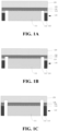
- the top surface of the ion implantation fence 113 can be formed at any position within the first type semiconductor layer 110. As shown in FIG. 1A , the trench 112 extends up through the first type semiconductor layer 110 and into an interior of the first type cap layer 114. A top surface of the trench 112 is higher than a top surface of the first type semiconductor layer 110. A top surface of the ion implantation fence 113 is lower than the top surface of the trench 112. FIG.
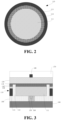
- FIG. 2 is a structural diagram showing a bottom view of the first exemplary micro LED as shown in FIG. 1A , according to some embodiments of the present disclosure.
- FIG. 2 shows a bottom view of the first type semiconductor layer 110 in which the ion implantation fence 113 is separated from the mesa structure 111 by the trench 112.
- the ion implantation fence 113 is formed around the trench and the trench is formed around the mesa structure 111. Since the trench extends up through the first type semiconductor layer 110 and into the interior of the first type cap layer 114, the first type cap layer 114 can be seen through the trench in the bottom view.
- the trench 112 extends up through the first type semiconductor layer 110 and the first type cap layer 114 and reaches the light emitting layer 130. In some embodiments, referring to FIG. 1B , the trench 112 extends up through the first type semiconductor layer 110 and the first type cap layer 114, and further extends into an interior of the light emitting layer 130. In some embodiments, the trench 112 extends up through the first type semiconductor layer 110, the first type cap layer 114 and the light emitting layer 130. Furthermore, in some embodiments, the trench 112 extends up through the first type semiconductor layer 110, the first type cap layer 114 and the light emitting layer 130, and further extends up into an interior of the second type cap layer 124. Furthermore, in some embodiments, referring to FIG. 1C , the trench 112 extends up through the first type semiconductor layer 110, the first type cap layer 114, the light emitting layer 130 and the second type cap layer 124, and further extends up into an interior of the second type semiconductor layer 120.
- the micro LED further includes a bottom contact 160.
- the bottom contact 160 is formed at the bottom of the first type semiconductor layer 110.
- An upper surface of the connection structure 150 is connected with the bottom contact 160 and a bottom surface of the connection structure 150 is connected with the IC backplane 190.
- the top contact 180 is made of metal or metal alloy, such as, AuGe, AuGeNi, etc.
- the top contact 180 is used for forming an ohmic contact between the top conductive layer 170 and the second type semiconductor layer 120, to optimize the electrical properties of the micro LED.
- the diameter of the top contact 180 is about 20-50 nm and the thickness of the top contact 180 is about 10 ⁇ 20nm.
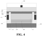
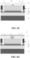
- FIG. 4 is a structural diagram showing a side sectional view of another variant of the first exemplary micro LED, according to some embodiments of the present disclosure.
- the connection structure 150 is a metal bonding layer for bonding the micro LED with the IC backplane 190.
- the bottom contact 160 is a bottom contact layer in this variant.
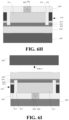
- FIG. 5 shows a flow chart of a method 500 for manufacturing the first exemplary micro LED, for example, the micro LED shown in FIG. 3 , according some embodiments of the present disclosure.
- the method 500 for manufacturing the micro LED includes steps 501-510.
- FIG. 6A to FIG. 6J are structural diagrams showing a side sectional view of a micro LED manufacturing process at each step (i.e., steps 501-510) corresponding to the method 500 shown in FIG. 5 , according to some embodiments of the present disclosure.
- the step 502 may further include: etching the first type semiconductor layer 610, the first type cap layer 614, and the light emitting layer 630 in sequence, and stopping the etching on the second type cap layer 624. As shown in FIG. 6B , the bottom surface of the first trench 612 contacts the second type cap layer 624, and locates on the second type cap layer 624.
- the first type semiconductor layer 610 is etched by a conventional dry etching process, such as, a plasma etching process, which can be understood be those skilled in the field.
- the step 502 may include: etching the first type semiconductor layer, the first type cap layer, the light emitting layer, the second type cap layer, and the second type semiconductor layer in sequence, and stopping the etching in the second type semiconductor layer. For example, referring back to, FIG. 1C , the top surface of the trench 121 contacts the second type semiconductor layer 120, and locates in the second type semiconductor layer 120.
- the first type semiconductor layer 110 is etched and the etching is stopped in the first type cap layer 114 to avoid the light emitting layer 130 being etched in the patterning process.
- the bottom of the trench 112 does not reach the light emitting layer 130.
- the first type semiconductor layer 110 is etched by a conventional dry etching process, such as, a plasma etching process, which can be understood be those skilled in the field.
- step 503 referring to FIG. 6C , a bottom contact 660 is deposited on the mesa structure 611.
- step 504 referring to FIG. 6D , an ion implantation process is performed into the fence 613'.
- the arrows illustrate a direction of the ion implantation process.
- a bottom isolation layer 640 is deposited on the whole substrate 600. That is, the bottom isolation layer 640 is deposited on the first type semiconductor layer 610. The first type semiconductor layer 610 and the bottom contact 660 are covered by the bottom isolation layer 640, and the trench 612 is filled by the bottom isolation layer 640.
- the bottom isolation layer 640 is deposited by a conventional chemical vapor deposition process.
- the bottom isolation layer can be formed at the sidewalls of the mesa structure 111, the first type semiconductor layer 110, the ion implantation fence 113, and the first type cap layer 114 in the first trench 112, and formed at a surface within the light emitting layer 130 in the first trench 112.
- the bottom isolation layer can be formed at the sidewalls of the mesa structure 111, the ion implantation fence 113, the first type cap layer 114, the light emitting layer 130, and the second type cap layer 124 in the trench 112, and formed at a surface within the second type semiconductor layer 120 in the trench 112.
- step 506 referring to FIG. 6F , the bottom isolation layer 640 is patterned to expose the bottom contact 660.
- the bottom isolation layer 640 is etched by a photo etching process and a dry etching process.
- a metal material 650' is deposited on the whole substrate 600. That is, the metal material 650' is deposited on the bottom isolation layer 640 and the bottom contact 660.
- the metal material is deposited by a conventional physical vapor deposition method.
- step 508 referring to FIG. 6H , the top of the metal material is ground to the top of the bottom isolation layer 640, to form a connection structure 650 such as a connection pillar.
- the metal material is ground by a Chemical Mechanical Polishing (CMP) process.
- connection pillar 650 is bonded with an IC backplane 690.
- the epitaxial structure is firstly turned upside down.
- the connection pillar 650 is bonded with a contact pad of the IC backplane 690 by a metal bonding process.
- the substrate 600 is removed by a conventional separation method, such as, a laser stripping method, or a chemical etching method.
- the arrows illustrate a removal direction of the substrate 600.
- a micro LED array panel is further provided by some embodiments of the present disclosure.
- the micro LED array panel includes a plurality of micro LEDs as described above and shown in FIGs. 1A-1F , FIG. 3 and FIG. 4 . These micro LEDs can be arranged in an array in the micro LED array panel.
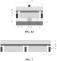
- FIG. 7 is a structural diagram showing a side sectional view of adjacent ones of the first exemplary micro LED, according to some embodiments of the present disclosure.
- a micro LED array panel includes a first type semiconductor layer 710, continuously formed in the micro LED array panel; a first type cap layer 714, continuously formed on the first type semiconductor layer 710; a light emitting layer 730, continuously formed on the first type cap layer 714; a second type cap layer 724, continuously formed on the light emitting layer 730; and a second type semiconductor layer 720, continuously formed on the second type cap layer 724.
- the material of the first type semiconductor layer 710 is selected from one or more of p-GaAs, p-GaP, p-AlInP, p-GaN, p-InGaN, or p-AlGaN.
- the material of the second type semiconductor layer 720 is selected from one or more of n-GaAs, n-AlInP, n-GaInP, n-AlGaAs, n-AlGaInP, n-GaN, n-InGaN, or n-AlGaN.
- a conductive type of the first type cap layer 714 is the same as the conductive type of the first type semiconductor layer 710 and a conductive type of the second type cap layer 724 is the same as the second type semiconductor layer 720.
- the first type semiconductor layer 710 includes multiple mesa structures 711, multiple trenches 712, and multiple ion implantation fences 713 separated from the mesa structures 711 by the trenches 712.
- the top surface of the ion implantation fence 713 is aligned with or lower than the top surface of the first type semiconductor layer 710. Thus, the ion implantation fence 713 cannot reach the light emitting layer 730.
- the top of the ion implantation fence 713 can be formed at any position. Additionally, the bottom surface of the ion implantation fence 713 can be formed at any position.
- the relationship of the top surface of the ion implantation fence 713, the top surface of the first type semiconductor layer 710, and the top surface of the trench 712 can be seen in the micro LED shown in FIGs. 1A-1E , the description of which will not be further described here. Additionally, the relationship of the bottom surface of the ion implantation fence 713 and the bottom surface of the first type semiconductor layer 710 can be seen in the micro LED shown in FIGs. 1E-1G, which will not be further described herein.
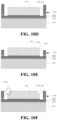
- the mesa structure can have one or multiple stair structures in another embodiment as seen in the mesa structure shown in FIG. 1H.
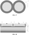
- FIG. 8 is a structural diagram showing a bottom view of the adjacent micro LEDs in FIG. 7 , according to some embodiments of the present disclosure.
- the ion implantation fences 713 are formed around the trench 712 and between the adjacent mesa structures 711. Furthermore, in each micro LED, the ion implantation fence 713 is formed around the trench 712 and the trench 712 is formed around the mesa structure 711. The electrical resistance of the ion implantation fence 713 is higher than the electrical resistance of the mesa structure 711. Since the trench extends up through the first type semiconductor layer 710 and through the first type cap layer 714, the light emitting layer 730 can be seen through the trench in the bottom view.
- the width of the ion implantation fence 713 can be not greater than 10% of the diameter of the mesa structure 711.
- the width of the ion implantation fence 713 is not greater than 200 nm.
- the micro LED array panel further includes a bottom contact 960 formed at the bottom of the first type semiconductor layer 910. Further detail of the bottom isolation layer 940, the IC backplane 990, the bottom contact 960 and the connection structure 950 are shown in the micro LED in FIGs. 3 and 4 , respectively as corresponding to the isolation layer 140, the IC backplane 190, the bottom contact 160, and the connection structure 150, which will not be further described.
- the width of the trench 1022 is not greater than 50% of the diameter of the mesa structure 1021. In some embodiments, the width of the trench 1022 is not greater than 10% of the diameter of the mesa structure 1021. Preferably, the width of the trench 1022 is not greater than 200 nm.
- the trench 1022 extend down through the bottom surface of the second type semiconductor layer 1020 and the second type cap layer 1024.
- the bottom surface of the ion implantation fence 1023 is higher than the bottom surface of the second trench 1022.
- the bottom surface of the ion implantation fence 1023 is aligned with the bottom surface of the second type semiconductor layer 1020.
- the top surface of the ion implantation fence 1023 can be formed at any position. In some embodiments, as shown in FIG. 10D , the top surface of the ion implantation fence 1023 is higher than the top surface of the second type semiconductor layer 1020. In some embodiments, as shown in FIG. 10E , the top surface of the ion implantation fence 1023 is lower than the top surface of the second type semiconductor layer 1020.
- the mesa structure 1021 includes one stair structure 1021a. In some embodiments, the mesa structure 1021 can have multiple stair structures.
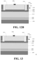
- FIGs. 12A and 12B are structural diagram showing a side sectional view of other variants of the second exemplary micro LED, according to some embodiments of the present disclosure.
- the micro LED further includes a bottom isolation layer 1040 formed under the first type semiconductor layer 1010.
- the material of the bottom isolation layer 1040 is selected from one or more of SiO2, SiNx, or Al2O3.
- An integrated circuit (IC) backplane 1090 is formed under the first type semiconductor layer 1010 and is electrically connected with the first type semiconductor layer 1010 via a connection structure 1050.
- the connection structure 1050 is a connection pillar.
- the micro LED further includes a bottom contact 1060 formed at the bottom of the first type semiconductor layer 1010.
- connection structure 1050 An upper surface of the connection structure 1050 is connected with a bottom contact 1060 and the bottom of the connection structure 1050 is connected with the IC backplane 1090.
- the bottom contact 1060 protrudes from the first type semiconductor layer 1010 as a bottom contact of the micro LED.
- the micro LED further includes a top contact 1080 and a top conductive layer 1070.
- the top contact 1080 is formed on the top of the second type semiconductor layer 1020.
- the top conductive layer 1070 is formed on the top surface of the second type semiconductor layer 1020 and the top surface of the top contact 1080, and covers the sidewalls of the second trench 1022.
- a dielectric layer 1071 is formed on a sidewall and bottom surface of the trench 1022.
- a conductive type of the top contact 1080 is the same as a conductive type of the second type semiconductor layer 1020.
- the conductive type of the second type semiconductor layer 1020 is N type and the conductive type of the top contact 1080 is N type.
- the top contact 1080 is made of metal or metal alloy, such as, AuGe, AuGeNi, etc.
- the top contact 1080 is used for forming an ohmic contact between the top conductive layer 1070 and the second type semiconductor layer 1020, to optimize the electrical properties of the micro LED.
- the diameter of the top contact 1080 is about 20-50 nm and the thickness of the top contact 1080 is about 10 ⁇ 20nm.
- connection structure 1050 can be a metal bonding layer for bonding the micro LED with the IC backplane 1090.
- the bottom contact 1060 is a bottom contact layer in this embodiment.
- FIG. 13 is a structural diagram showing a side sectional view of another variant of the second exemplary micro LED, according to some embodiments of the present disclosure.
- a dielectric layer 1071 can be full filled in the second trench 1022.
- a conductive layer 1070 is formed on the whole substrate.
- the dielectric layer 1071 can be formed on the top surface of second type semiconductor layer 1020.
- the dielectric layer can be a multiple layer structure, and the material for a first portion of the dielectric layer in the trench and the material for a second portion of the dielectric layer can be different.
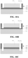
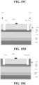
- FIG. 14 shows a flow chart of a method 1400 for manufacturing the second exemplary micro LED, for example the micro LED shown in FIG. 13 , according some embodiments of the present disclosure.
- the method for manufacturing the micro LED includes steps 1401-1406.
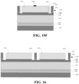
- FIGs. 15A-15F are structural diagrams showing a side sectional view of a micro LED manufacturing process at each step (i.e., steps 1401 to 1406) of the method 1400 shown in FIG. 14 , according to some embodiments of the present disclosure.
- a bottom contact layer 1560 used as the bottom contact is deposited on the top surface of the first type semiconductor layer 1510. Then, a metal bonding layer which is used as a connection structure 1550 is deposited on the top surface of the bottom contact layer 1560.
- the step 1403 further includes: etching the second type semiconductor layer and the second type cap layer, and stopping the etching on the top surface of the light emitting layer 1030, to avoid the light emitting layer being etched in the patterning process. As shown in FIG. 15C , the bottom surface of the trench 1522 contacts the light emitting layer 1530.
- the step 1403 further includes: etching the second type semiconductor layer and the light emitting layer in sequence, and stopping the etching in the light emitting layer 1030. Referring back to FIG. 10B , the bottom surface of the trench 1022 contacts the light emitting layer 1030, and is located in the light emitting layer 1030.
- a top contact 1580 is deposited on the mesa structure 1521.
- a first protective mask (not shown) is used to protect an area where the top contact 1580 will not be formed.
- the material of the top contact 1580 is deposited on the first protective mask and on the second type semiconductor layer 1520 by a conventional vapor deposition process, such as a physical vapor deposition process or a chemical vapor deposition process.
- the first protective mask is removed from the second type semiconductor layer 1520 and the material on the first protective mask is also removed with the first protective mask to form the top contact 1580 on the mesa structure 1521.
- a dielectric layer 1571 is formed on the sidewalls and the bottom surface of the trench 1522. As shown in FIG. 15F , the dielectric layer 1571 is formed on the sidewall of the second type semiconductor layer 1520, the mesa structure 1521, and the second type cap layer 1524 in the trench 1522 and on the surface of the light emitting layer 1530 in the trench 1522. In some embodiments, referring back to FIG. 10B , the dielectric layer can be formed on the sidewall of the second type semiconductor layer 1020, the mesa structure 1021, and the light emitting layer 1030 in the trench 1022 and on the surface of the light emitting layer 1030 in the trench 1022. In some embodiments, referring back to FIG.
- the dielectric layer can be formed on the sidewall of the mesa structure 1021, the second type cap layer 1024, the light emitting layer 1030, the first type cap layer 1014, and on the sidewall and surface of the first type semiconductor layer 1010 in the trench 1022.
- a micro LED array panel is further provided according to some embodiments of the present disclosure.
- the micro LED array panel includes a plurality of micro LEDs as described above shown in FIGs. 10A-10H, FIGs. 12A , 12B and FIG. 13 . These micro LEDs can be arranged in an array in the micro LED array panel.
- FIG. 16 is a structural diagram showing a side sectional view of adjacent ones of the second exemplary micro LED, according to some embodiments of the present disclosure.
- a micro LED array panel includes a first type semiconductor layer 1610, continuously formed in the micro LED array panel; a first type cap layer 1614, continuously formed on the first type semiconductor layer 1610; a light emitting layer 1630, continuously formed on the first type semiconductor layer 1610; a second type cap layer 1624, continuously formed on the light emitting layer 1630; and a second type semiconductor layer 1620, continuously formed on the second type cap layer 1624.
- the space between the adjacent sidewalls of adjacent ones of the mesa structures 1621 can be adjusted.
- the space between the adjacent sidewalls of the mesa structures 1621 is not greater than 50% of the diameter of the mesa structure 1621.
- the space between the adjacent sidewalls of the mesa structures 1621 is not greater than 30% of the diameter of the mesa structure 1621.
- the space between the adjacent sidewalls of the mesa structures 1621 is not greater than 600 nm.
- the width of the ion implantation fence 1623 can be adjusted.
- the width of the ion implantation fence 1623 can be not greater than 50% of the diameter of the mesa structure 1621.
- the width of the ion implantation fence 1623 can be not greater than 10% of the diameter of the mesa structure 1621.
- the width of the ion implantation fence 1623 is not greater than 200 nm.
- FIG. 18 is a structural diagram showing a side sectional view of adjacent ones of the micro LED in FIG. 12B in a micro LED array panel, according to some embodiments of the present disclosure.
- the micro LED array panel further includes a top contact 1880, a dielectric layer 1871, and a top conductive layer 1870. Further details of the top contact 1880, the dielectric layer 1871 and the top conductive layer 1870 can be understood by also referring to the micro LEDs shown in FIGs. 10A-10F , FIGs. 12A and 12B and FIG. 13 , which will not be further described here.
- the first mesa structure 1911 can have one or multiple stair structures, as shown in FIG. 1H.
- the second mesa structure 1921 can have one or multiple stair structures, as shown in FIG. 10H.
- the micro LED further includes a top contact 2080 and a top conductive layer 2070.
- the top contact 2080 is formed on the top of a second type semiconductor layer 2020.
- the top conductive layer 2070 is formed on the top of the second type semiconductor layer 2020 and the top contact 2080 and covers the sidewalls and bottom of the second trench 2022. Further details regarding the top contact 2080 and the top conductive layer 2070 can be found by referring to the description for Embodiment 2, which will not be further described here.
- Process I the first type semiconductor layer is patterned, and then ions are implanted into the first type semiconductor layer to form a first ion implantation fence.
- the Process I at least includes steps 2101-2109, and the Process II at least includes steps 2110-2113.
- the steps 2101-2109 are similar to the steps 501-509 of method 500 as shown in FIG. 5 .
- the side sectional views for the micro LED being manufactured according to steps 2101-2109 are similar to the views shown in FIGs. 6A-6I .
- step 2101 referring to FIG. 6A , the epitaxial structure is provided.
- the epitaxial structure includes the first type semiconductor layer 610, the first type cap layer 614, the light emitting layer 630, the second type cap layer 624 and the second type semiconductor layer 620 sequentially from top to bottom.
- the first type semiconductor layer 610 is patterned to form the mesa structure 611, the trench 612 and the fence 613'.
- step 2104 referring to FIG. 6D , an ion implantation process is performed into the fence 613'.
- step 2105 referring to FIG. 6E , the isolation layer 640 is deposited on the whole substrate 600.
- the bottom isolation layer can be filled into the first trench.
- the bottom isolation layer can be formed on the sidewalls of the first mesa structure, the first ion implantation fence, the first type semiconductor layer, the first type cap layer, the light emitting layer and the second type semiconductor layer, the second mesa structure, the second type cap layer, and the second type ion implantation fence in the first trench, which depends on a depth of the first trench.
- step 2106 referring to FIG. 6F , the isolation layer 640 is patterned to expose the bottom contact 660.
- step 2107 referring to FIG. 6G , metal material 650' is deposited on the whole substrate 600.
- step 2109 referring to FIG. 6I , the connection pillar 650 is bonded with the IC backplane 690, and the substructure 600 is removed.
- FIGs. 22A-22D are structural diagrams showing a side sectional view of the micro LED manufacturing process at steps 2110-2113 of the method 2100 shown in FIG. 21 , according to some embodiments of the present disclosure.
- a second type semiconductor layer 2220 is patterned to form a mesa structure 2221, a trench 2222 and a fence 2223'.
- FIGs. 23A and 23B are structural diagrams showing a side sectional view of other variants of a third exemplary micro LED, according to some embodiments of the present disclosure.
- a bottom isolation layer 2340 is filled in the first trench 2312, and formed on the sidewall of a first mesa structure 2311, a first ion implantation fence 2313, a first type cap layer 2314, and a light emitting layer 2330 in the first trench 2312.
- a dielectric layer 2371 is formed extending into a second trench 2322.
- the dielectric layer 2371 is formed on the sidewall and the bottom of a second trench 2322.
- the dielectric layer 2371 is formed on the sidewall of a second mesa structure 2321, a second type semiconductor layer 2320, a second ion implantation fence 2323, a second type cap layer 2324, and a light emitting layer 2330 in the second trench 2322. Then the top conductive layer 2370 is formed on the surface of the dielectric layer 2371 extending into the second trench 2322, and formed on the top of the second mesa structure 2321 and the top of second ion implantation fence 2323.
- the bottom isolation layer 2340 is filled in the first trench 2312, and formed on the sidewall of the first mesa structure 2311, the first ion implantation fence 2313, and the first type semiconductor layer 2310.
- the top conductive layer 2370 can be formed extending into the second trench 2322.
- the dielectric layer 2371 is formed extending into the second trench 2322.
- the bottom isolation layer 2340 is formed on the sidewalls and the top of the first trench 2312
- the dielectric layer 2371 is formed on the sidewalls and the bottom of the second trench 2322.
- the thickness of the bottom isolation layer extending into the first trench 2312 depends on a position of the bottom of the second trench 2322 and a position of the top of the first trench 2312.
- the thickness of the dielectric layer 2371 extending into the second trench 2322 depends on a position of the bottom of the second trench 2322 and a position of the top of the first trench 2312.
- a top contact and a bottom contact can be formed on the micro LED according to some embodiments of the present disclosure, which will not be further described here.
- a micro LED array panel is further provided according to some embodiments of the present disclosure.
- the micro LED array panel includes a plurality of micro LEDs as described above and shown in FIGs. 19A-19E , FIG. 20 and FIG. 23A and 23B. These micro LEDs can be arranged in an array in the micro LED array panel.
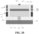
- FIG. 24 is a structural diagram showing a side sectional view of adjacent ones of the micro LED in FIG. 23A in a micro LED array panel, according to some embodiments of the present disclosure.
- the micro LED array panel at least includes a first type semiconductor layer 2410 continuously formed in the micro LED array panel; a first type cap layer 2414, continuously formed on the first type semiconductor layer 2410; a light emitting layer 2430 continuously formed on the first type cap layer 2414; a second type cap layer 2424, continuously formed on the light emitting layer 2330; and a second type semiconductor layer 2420, formed on the second type cap layer 2324.
- the first type semiconductor layer 2410 includes multiple first mesa structures 2411, multiple first trenches 2412, and multiple first ion implantation fences 2413 separated from the first mesa structures via the first trenches 2412.
- the top surface of the first ion implantation fence 2413 is lower than the top surface of the first type semiconductor layer 2410.
- a bottom view of the micro LED array panel without an IC backplane is similar to the bottom view shown in FIG. 8 .
- the first ion implantation fences 2413 are formed around the first trenches 2412 and between the adjacent first type mesa structures 2411.
- the electrical resistance of the first ion implantation fence 2413 is higher than the electrical resistance of the first mesa structure 2411.
- the first ion implantation fence 2413 is formed around the first trench 2412 and the first trench 2412 is formed around the first mesa structure 2411.
- the second type semiconductor layer 2420 includes multiple second mesa structures 2421, multiple second trenches 2422, and multiple second ion implantation fences 2423 separated from the second mesa structures 2421 via the second trenches 2422.
- the bottom surface of the second ion implantation fence 2423 is higher than the bottom surface of the second type semiconductor layer 2420.
- a top view of the micro LED array panel is similar to the top view shown in FIG. 17 in that the second ion implantation fences 2423 being formed around the second trenches 2422 and between the adjacent second mesa structures 2421.
- the electrical resistance of the second ion implantation fence 2423 is higher than the electrical resistance of the second mesa structure 2421.
- the second ion implantation fence 2323 is formed around the second trench 2422 and the second trench 2422 is formed around the second mesa structure 2421.
- the width of the first ion implantation fence 2413 is not greater than 50% of the diameter of the first mesa structure 2411. In some embodiments, the width of the first ion implantation fence 2313 is not greater than 10% of the diameter of the first mesa structure 2311. Preferably, in some embodiments, in the micro LED array panel, the width of the first ion implantation fence 2413 is not greater than 200 nm.
- the space between the adjacent sidewalls of the second mesa structure 2421 is not greater than 50% of the diameter of the second mesa structure 2421. In some embodiments, the space between the adjacent sidewalls of the second mesa structure 2421 is not greater than 30% of the diameter of the second mesa structure 2421.
Landscapes
- Led Devices (AREA)
- Engineering & Computer Science (AREA)
- Microelectronics & Electronic Packaging (AREA)
- Power Engineering (AREA)
- Physics & Mathematics (AREA)
- Condensed Matter Physics & Semiconductors (AREA)
- General Physics & Mathematics (AREA)
- Computer Hardware Design (AREA)
- Led Device Packages (AREA)
Priority Applications (1)
| Application Number | Priority Date | Filing Date | Title |
|---|---|---|---|
| EP25158677.2A EP4535962A3 (de) | 2022-01-31 | 2022-01-31 | Mikro-led, mikro-led-array-tafel und herstellungsverfahren dafür |
Applications Claiming Priority (3)
| Application Number | Priority Date | Filing Date | Title |
|---|---|---|---|
| EP22922964.6A EP4473586A4 (de) | 2022-01-31 | 2022-01-31 | Mikro-led, mikro-led-array-tafel und herstellungsverfahren dafür |
| PCT/CN2022/075282 WO2023142140A1 (en) | 2022-01-31 | 2022-01-31 | Micro led, micro led array panel and manufacuturing method thereof |
| EP25158677.2A EP4535962A3 (de) | 2022-01-31 | 2022-01-31 | Mikro-led, mikro-led-array-tafel und herstellungsverfahren dafür |
Related Parent Applications (1)
| Application Number | Title | Priority Date | Filing Date |
|---|---|---|---|
| EP22922964.6A Division EP4473586A4 (de) | 2022-01-31 | 2022-01-31 | Mikro-led, mikro-led-array-tafel und herstellungsverfahren dafür |
Publications (2)
| Publication Number | Publication Date |
|---|---|
| EP4535962A2 true EP4535962A2 (de) | 2025-04-09 |
| EP4535962A3 EP4535962A3 (de) | 2025-06-18 |
Family
ID=87432578
Family Applications (6)
| Application Number | Title | Priority Date | Filing Date |
|---|---|---|---|
| EP25158792.9A Pending EP4539640A3 (de) | 2022-01-31 | 2022-01-31 | Mikro-led, mikro-led-array-tafel und herstellungsverfahren dafür |
| EP25158836.4A Pending EP4535964A3 (de) | 2022-01-31 | 2022-01-31 | Mikro-led, mikro-led-array-tafel und herstellungsverfahren dafür |
| EP25158677.2A Pending EP4535962A3 (de) | 2022-01-31 | 2022-01-31 | Mikro-led, mikro-led-array-tafel und herstellungsverfahren dafür |
| EP22922964.6A Pending EP4473586A4 (de) | 2022-01-31 | 2022-01-31 | Mikro-led, mikro-led-array-tafel und herstellungsverfahren dafür |
| EP25158689.7A Pending EP4539639A3 (de) | 2022-01-31 | 2022-01-31 | Mikro-led, mikro-led-array-tafel und herstellungsverfahren dafür |
| EP25158654.1A Pending EP4535963A3 (de) | 2022-01-31 | 2022-01-31 | Mikro-led, mikro-led-array-tafel und herstellungsverfahren dafür |
Family Applications Before (2)
| Application Number | Title | Priority Date | Filing Date |
|---|---|---|---|
| EP25158792.9A Pending EP4539640A3 (de) | 2022-01-31 | 2022-01-31 | Mikro-led, mikro-led-array-tafel und herstellungsverfahren dafür |
| EP25158836.4A Pending EP4535964A3 (de) | 2022-01-31 | 2022-01-31 | Mikro-led, mikro-led-array-tafel und herstellungsverfahren dafür |
Family Applications After (3)
| Application Number | Title | Priority Date | Filing Date |
|---|---|---|---|
| EP22922964.6A Pending EP4473586A4 (de) | 2022-01-31 | 2022-01-31 | Mikro-led, mikro-led-array-tafel und herstellungsverfahren dafür |
| EP25158689.7A Pending EP4539639A3 (de) | 2022-01-31 | 2022-01-31 | Mikro-led, mikro-led-array-tafel und herstellungsverfahren dafür |
| EP25158654.1A Pending EP4535963A3 (de) | 2022-01-31 | 2022-01-31 | Mikro-led, mikro-led-array-tafel und herstellungsverfahren dafür |
Country Status (7)
| Country | Link |
|---|---|
| US (1) | US20230246131A1 (de) |
| EP (6) | EP4539640A3 (de) |
| JP (1) | JP2025503794A (de) |
| KR (1) | KR20240144300A (de) |
| CN (1) | CN118679586B (de) |
| TW (2) | TWI842358B (de) |
| WO (1) | WO2023142140A1 (de) |
Families Citing this family (1)
| Publication number | Priority date | Publication date | Assignee | Title |
|---|---|---|---|---|
| WO2023142141A1 (en) * | 2022-01-31 | 2023-08-03 | Jade Bird Display (Shanghai) Company | Micro led, micro led array panel and manufacuturing method thereof |
Family Cites Families (33)
| Publication number | Priority date | Publication date | Assignee | Title |
|---|---|---|---|---|
| US6255129B1 (en) * | 2000-09-07 | 2001-07-03 | Highlink Technology Corporation | Light-emitting diode device and method of manufacturing the same |
| JP4151282B2 (ja) * | 2002-03-01 | 2008-09-17 | 日亜化学工業株式会社 | 窒化物系半導体発光素子 |
| EP1868239B1 (de) * | 2006-06-12 | 2020-04-22 | ams AG | Verfahren zur Herstellung von Isolationsgräben in einer Halbleiterscheibe |
| US8193559B2 (en) * | 2009-01-27 | 2012-06-05 | Infineon Technologies Austria Ag | Monolithic semiconductor switches and method for manufacturing |
| US8263422B2 (en) * | 2010-04-26 | 2012-09-11 | Varian Semiconductor Equipment Associates, Inc. | Bond pad isolation and current confinement in an LED using ion implantation |
| US8658513B2 (en) * | 2010-05-04 | 2014-02-25 | Varian Semiconductor Equipment Associates, Inc. | Isolation by implantation in LED array manufacturing |
| JP6035736B2 (ja) * | 2011-10-26 | 2016-11-30 | ソニー株式会社 | 発光素子およびその製造方法、並びに発光装置 |
| US20130292719A1 (en) * | 2012-05-04 | 2013-11-07 | Chi Mei Lighting Technology Corp. | Light-emitting diode structure and method for manufacturing the same |
| CN102820315B (zh) * | 2012-08-20 | 2015-10-28 | 北京工业大学 | 一种直接发光型微显示阵列器件及其制备方法 |
| TWI552382B (zh) * | 2014-01-24 | 2016-10-01 | 隆達電子股份有限公司 | 發光二極體裝置及其製造方法 |
| US9625647B2 (en) * | 2014-01-29 | 2017-04-18 | The University Of Connecticut | Optoelectronic integrated circuit |
| CN105489722B (zh) * | 2014-10-08 | 2018-10-26 | 展晶科技(深圳)有限公司 | 发光二极管封装结构、发光二极管晶粒及其制造方法 |
| US10418519B2 (en) * | 2015-12-22 | 2019-09-17 | Apple Inc. | LED sidewall processing to mitigate non-radiative recombination |
| KR102435523B1 (ko) * | 2016-03-10 | 2022-08-23 | 삼성전자주식회사 | 발광 소자 및 이의 제조 방법 |
| WO2017184686A1 (en) * | 2016-04-19 | 2017-10-26 | The Penn State Research Foundation | Gap-free microdisplay based on iii-nitride led arrays |
| TWI648870B (zh) * | 2016-12-09 | 2019-01-21 | 英屬開曼群島商錼創科技股份有限公司 | 發光二極體晶片 |
| CN107170671A (zh) * | 2017-06-22 | 2017-09-15 | 广东省半导体产业技术研究院 | 一种基于离子注入的GaN功率器件及其制造方法 |
| US10163680B1 (en) * | 2017-09-19 | 2018-12-25 | Texas Instruments Incorporated | Sinker to buried layer connection region for narrow deep trenches |
| CN111602250B (zh) * | 2018-02-07 | 2023-08-11 | 艾鲍尔半导体 | 具有用于场截止和反向传导的三维背侧结构的igbt器件 |
| WO2020000184A1 (zh) * | 2018-06-26 | 2020-01-02 | 苏州晶湛半导体有限公司 | 半导体结构及其制造方法 |
| JP7398818B2 (ja) * | 2018-08-10 | 2023-12-15 | ビジョンラボ コーポレーション | 流体トランスファーシステムおよびマイクロled装置の製造方法 |
| CN110957399B (zh) * | 2018-09-26 | 2021-04-30 | 中国科学院苏州纳米技术与纳米仿生研究所 | 半导体光电子器件的制作方法 |
| US10910514B1 (en) * | 2018-10-05 | 2021-02-02 | Facebook Technologies, Llc | Molded etch masks |
| KR102698293B1 (ko) * | 2018-11-27 | 2024-08-23 | 삼성전자주식회사 | 디스플레이 장치 및 제조 방법 |
| EP3667721A1 (de) * | 2018-12-10 | 2020-06-17 | IMEC vzw | Verfahren zur herstellung einer optischen vorrichtung |
| CN110010542A (zh) * | 2019-04-18 | 2019-07-12 | 广东省半导体产业技术研究院 | 微型led器件、微型led阵列及制造方法 |
| CN111477726A (zh) * | 2019-05-08 | 2020-07-31 | 伊乐视有限公司 | 用于流体组装的平面表面贴装微型led及其制备方法 |
| CN110993758B (zh) * | 2019-10-31 | 2020-12-22 | 华灿光电(苏州)有限公司 | 微型发光二极管的显示阵列及其制作方法 |
| US11569415B2 (en) * | 2020-03-11 | 2023-01-31 | Lumileds Llc | Light emitting diode devices with defined hard mask opening |
| US12113091B2 (en) * | 2020-05-05 | 2024-10-08 | Raysolve Optoelectronics (Suzhou) Company Limited | Full color light emitting diode structure and method for manufacturing the same |
| CN112768574B (zh) * | 2021-04-08 | 2021-06-18 | 度亘激光技术(苏州)有限公司 | 半导体结构的形成方法 |
| CN113889560B (zh) * | 2021-09-14 | 2024-03-08 | 深圳市洲明科技股份有限公司 | Led芯片及其制备方法和封装方法 |
| WO2023142143A1 (en) * | 2022-01-31 | 2023-08-03 | Jade Bird Display (Shanghai) Company | Micro led, micro led array panel and manufacuturing method thereof |
-
2022
- 2022-01-31 EP EP25158792.9A patent/EP4539640A3/de active Pending
- 2022-01-31 WO PCT/CN2022/075282 patent/WO2023142140A1/en not_active Ceased
- 2022-01-31 EP EP25158836.4A patent/EP4535964A3/de active Pending
- 2022-01-31 CN CN202280090586.8A patent/CN118679586B/zh active Active
- 2022-01-31 EP EP25158677.2A patent/EP4535962A3/de active Pending
- 2022-01-31 EP EP22922964.6A patent/EP4473586A4/de active Pending
- 2022-01-31 JP JP2024544902A patent/JP2025503794A/ja not_active Withdrawn
- 2022-01-31 EP EP25158689.7A patent/EP4539639A3/de active Pending
- 2022-01-31 KR KR1020247029124A patent/KR20240144300A/ko active Pending
- 2022-01-31 EP EP25158654.1A patent/EP4535963A3/de active Pending
-
2023
- 2023-01-30 TW TW112103119A patent/TWI842358B/zh active
- 2023-01-30 TW TW112150105A patent/TWI883725B/zh active
- 2023-01-30 US US18/161,446 patent/US20230246131A1/en active Pending
Also Published As
| Publication number | Publication date |
|---|---|
| CN118679586A (zh) | 2024-09-20 |
| EP4535964A3 (de) | 2025-06-25 |
| CN118679586B (zh) | 2026-02-13 |
| JP2025503794A (ja) | 2025-02-04 |
| EP4539640A3 (de) | 2025-06-18 |
| EP4473586A4 (de) | 2025-11-19 |
| KR20240144300A (ko) | 2024-10-02 |
| EP4539640A2 (de) | 2025-04-16 |
| TWI842358B (zh) | 2024-05-11 |
| EP4535962A3 (de) | 2025-06-18 |
| EP4535963A2 (de) | 2025-04-09 |
| TW202418619A (zh) | 2024-05-01 |
| EP4535964A2 (de) | 2025-04-09 |
| US20230246131A1 (en) | 2023-08-03 |
| EP4539639A3 (de) | 2025-07-02 |
| EP4535963A3 (de) | 2025-06-18 |
| WO2023142140A1 (en) | 2023-08-03 |
| TW202347825A (zh) | 2023-12-01 |
| TWI883725B (zh) | 2025-05-11 |
| EP4539639A2 (de) | 2025-04-16 |
| EP4473586A1 (de) | 2024-12-11 |
Similar Documents
| Publication | Publication Date | Title |
|---|---|---|
| EP4583670A2 (de) | Mikro-led, mikro-led-array-tafel und herstellungsverfahren dafür | |
| WO2023142143A1 (en) | Micro led, micro led array panel and manufacuturing method thereof | |
| EP4535962A2 (de) | Mikro-led, mikro-led-array-tafel und herstellungsverfahren dafür | |
| EP4518616A2 (de) | Mikro-led, mikro-led-array-tafel und herstellungsverfahren dafür |
Legal Events
| Date | Code | Title | Description |
|---|---|---|---|
| PUAI | Public reference made under article 153(3) epc to a published international application that has entered the european phase |
Free format text: ORIGINAL CODE: 0009012 |
|
| STAA | Information on the status of an ep patent application or granted ep patent |
Free format text: STATUS: THE APPLICATION HAS BEEN PUBLISHED |
|
| AC | Divisional application: reference to earlier application |
Ref document number: 4473586 Country of ref document: EP Kind code of ref document: P |
|
| AK | Designated contracting states |
Kind code of ref document: A2 Designated state(s): AL AT BE BG CH CY CZ DE DK EE ES FI FR GB GR HR HU IE IS IT LI LT LU LV MC MK MT NL NO PL PT RO RS SE SI SK SM TR |
|
| PUAL | Search report despatched |
Free format text: ORIGINAL CODE: 0009013 |
|
| AK | Designated contracting states |
Kind code of ref document: A3 Designated state(s): AL AT BE BG CH CY CZ DE DK EE ES FI FR GB GR HR HU IE IS IT LI LT LU LV MC MK MT NL NO PL PT RO RS SE SI SK SM TR |
|
| RIC1 | Information provided on ipc code assigned before grant |
Ipc: H10H 29/14 20250101ALI20250514BHEP Ipc: H10H 20/857 20250101ALI20250514BHEP Ipc: H10H 20/852 20250101ALI20250514BHEP Ipc: H10H 20/819 20250101ALI20250514BHEP Ipc: H10H 20/816 20250101ALI20250514BHEP Ipc: H10H 20/01 20250101AFI20250514BHEP |