EP4535554A1 - Dc block structure - Google Patents
Dc block structure Download PDFInfo
- Publication number
- EP4535554A1 EP4535554A1 EP22943754.6A EP22943754A EP4535554A1 EP 4535554 A1 EP4535554 A1 EP 4535554A1 EP 22943754 A EP22943754 A EP 22943754A EP 4535554 A1 EP4535554 A1 EP 4535554A1
- Authority
- EP
- European Patent Office
- Prior art keywords
- transmission line
- block structure
- dielectric
- characteristic impedance
- transmission
- Prior art date
- Legal status (The legal status is an assumption and is not a legal conclusion. Google has not performed a legal analysis and makes no representation as to the accuracy of the status listed.)
- Pending
Links
Images







Classifications
-
- H—ELECTRICITY
- H01—ELECTRIC ELEMENTS
- H01P—WAVEGUIDES; RESONATORS, LINES, OR OTHER DEVICES OF THE WAVEGUIDE TYPE
- H01P1/00—Auxiliary devices
- H01P1/20—Frequency-selective devices, e.g. filters
- H01P1/2007—Filtering devices for biasing networks or DC returns
-
- H—ELECTRICITY
- H01—ELECTRIC ELEMENTS
- H01G—CAPACITORS; CAPACITORS, RECTIFIERS, DETECTORS, SWITCHING DEVICES, LIGHT-SENSITIVE OR TEMPERATURE-SENSITIVE DEVICES OF THE ELECTROLYTIC TYPE
- H01G2/00—Details of capacitors not covered by a single one of groups H01G4/00-H01G11/00
- H01G2/02—Mountings
- H01G2/06—Mountings specially adapted for mounting on a printed-circuit support
-
- H—ELECTRICITY
- H01—ELECTRIC ELEMENTS
- H01G—CAPACITORS; CAPACITORS, RECTIFIERS, DETECTORS, SWITCHING DEVICES, LIGHT-SENSITIVE OR TEMPERATURE-SENSITIVE DEVICES OF THE ELECTROLYTIC TYPE
- H01G4/00—Fixed capacitors; Processes of their manufacture
- H01G4/002—Details
- H01G4/228—Terminals
-
- H—ELECTRICITY
- H01—ELECTRIC ELEMENTS
- H01G—CAPACITORS; CAPACITORS, RECTIFIERS, DETECTORS, SWITCHING DEVICES, LIGHT-SENSITIVE OR TEMPERATURE-SENSITIVE DEVICES OF THE ELECTROLYTIC TYPE
- H01G4/00—Fixed capacitors; Processes of their manufacture
- H01G4/30—Stacked capacitors
-
- H—ELECTRICITY
- H01—ELECTRIC ELEMENTS
- H01G—CAPACITORS; CAPACITORS, RECTIFIERS, DETECTORS, SWITCHING DEVICES, LIGHT-SENSITIVE OR TEMPERATURE-SENSITIVE DEVICES OF THE ELECTROLYTIC TYPE
- H01G4/00—Fixed capacitors; Processes of their manufacture
- H01G4/33—Thin- or thick-film capacitors (thin- or thick-film circuits; capacitors without a potential-jump or surface barrier specially adapted for integrated circuits, details thereof, multistep manufacturing processes therefor)
-
- H—ELECTRICITY
- H01—ELECTRIC ELEMENTS
- H01G—CAPACITORS; CAPACITORS, RECTIFIERS, DETECTORS, SWITCHING DEVICES, LIGHT-SENSITIVE OR TEMPERATURE-SENSITIVE DEVICES OF THE ELECTROLYTIC TYPE
- H01G4/00—Fixed capacitors; Processes of their manufacture
- H01G4/40—Structural combinations of fixed capacitors with other electric elements, the structure mainly consisting of a capacitor, e.g. RC combinations
-
- H—ELECTRICITY
- H01—ELECTRIC ELEMENTS
- H01P—WAVEGUIDES; RESONATORS, LINES, OR OTHER DEVICES OF THE WAVEGUIDE TYPE
- H01P5/00—Coupling devices of the waveguide type
- H01P5/02—Coupling devices of the waveguide type with invariable factor of coupling
- H01P5/022—Transitions between lines of the same kind and shape, but with different dimensions
- H01P5/028—Transitions between lines of the same kind and shape, but with different dimensions between strip lines
-
- H—ELECTRICITY
- H05—ELECTRIC TECHNIQUES NOT OTHERWISE PROVIDED FOR
- H05K—PRINTED CIRCUITS; CASINGS OR CONSTRUCTIONAL DETAILS OF ELECTRIC APPARATUS; MANUFACTURE OF ASSEMBLAGES OF ELECTRICAL COMPONENTS
- H05K1/00—Printed circuits
- H05K1/02—Details
- H05K1/0213—Electrical arrangements not otherwise provided for
- H05K1/0237—High frequency adaptations
- H05K1/025—Impedance arrangements, e.g. impedance matching, reduction of parasitic impedance
-
- H—ELECTRICITY
- H05—ELECTRIC TECHNIQUES NOT OTHERWISE PROVIDED FOR
- H05K—PRINTED CIRCUITS; CASINGS OR CONSTRUCTIONAL DETAILS OF ELECTRIC APPARATUS; MANUFACTURE OF ASSEMBLAGES OF ELECTRICAL COMPONENTS
- H05K1/00—Printed circuits
- H05K1/18—Printed circuits structurally associated with non-printed electric components
- H05K1/181—Printed circuits structurally associated with non-printed electric components associated with surface mounted components
-
- H—ELECTRICITY
- H05—ELECTRIC TECHNIQUES NOT OTHERWISE PROVIDED FOR
- H05K—PRINTED CIRCUITS; CASINGS OR CONSTRUCTIONAL DETAILS OF ELECTRIC APPARATUS; MANUFACTURE OF ASSEMBLAGES OF ELECTRICAL COMPONENTS
- H05K2201/00—Indexing scheme relating to printed circuits covered by H05K1/00
- H05K2201/10—Details of components or other objects attached to or integrated in a printed circuit board
- H05K2201/10007—Types of components
- H05K2201/10015—Non-printed capacitor
Definitions
- the present invention relates to a DC block structure using a surface mount capacitor.
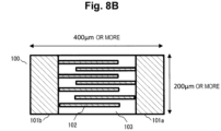
- Fig. 8A is a front view of an MLCC
- Fig. 8B is a sectional view of the MLCC.
- An MLCC 100 includes two electrodes 101a and 101b, and has a structure in which an electrode layer 102 and a high dielectric 103 made of ceramics are alternately stacked.
- the MLCC has a problem that parasitic capacitances are likely to occur in the electrodes 101a and 101b, and it is difficult to use the MLCC in a region of 100 GHz or more due to characteristic deterioration.
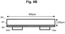
- Fig. 9A is a front view of a silicon capacitor
- Fig. 9B is a sectional view of the silicon capacitor.
- a silicon capacitor 200 has a structure in which a thin film capacitor 202 is formed on a silicon substrate 201. Further, bumps 203a and 203b are formed so as to be connected with an electrode of the thin film capacitor 202. Since the silicon capacitor is formed with the thin film in capacitance, there is an advantage that the silicon capacitor is close to a structure of a transmission line and characteristic deterioration hardly occurs even in a high frequency range. However, the silicon capacitor has a problem that when a characteristic is further extended to the vicinity of 150 GHz, characteristic deterioration occurs in the vicinity of 125 GHz in a conventional mounting structure, and desired performance cannot be obtained.
- Fig. 10A shows a plan view of a conventional DC block structure using a silicon capacitor
- Fig. 10B shows a sectional view of the DC block structure.
- the silicon capacitor 200 is inserted between a transmission line 204a and a transmission line 204b.
- the transmission lines 204a and 204b are formed on a surface of a dielectric 205.
- a ground conductor 206 is formed on a back surface of the dielectric 205.
- the silicon capacitor 200 is connected with the transmission lines 204a and 204b via the bumps 203a and 203b (see Non Patent Literature 1).
- a roll-off characteristic in which an insertion loss increases at a frequency of 150 GHz or less occurs.
- An equivalent circuit of a portion of the bump 203a indicated by a broken line 207 in Fig. 10B is as shown in Fig. 11 .
- L represents an inductive component
- C1 represents a capacitive component generated on the silicon capacitor 200 side
- C2 represents a capacitive component generated on the transmission line 204a side.
- the reason why the roll-off characteristic is generated at the frequency of 150 GHz or less is that portions of the bumps 203a and 203b act as low-pass filters in this manner.
- a DC block structure includes: a dielectric; a first transmission line formed on a surface of the dielectric; a second transmission line formed on the surface of the dielectric and designed so that characteristic impedance is the same as characteristic impedance of the first transmission line; a third transmission line formed on the surface of the dielectric so as to be connected with the first transmission line and designed so that characteristic impedance is higher than the characteristic impedance of the first and second transmission lines; a fourth transmission line formed on the surface of the dielectric so as to be connected with the second transmission line and designed so that characteristic impedance is higher than the characteristic impedance of the first and second transmission lines; and a capacitor mounted on the third and fourth transmission lines so as to connect the third transmission line and the fourth transmission line in series.
- a frequency characteristic of the DC block structure can have a peaking characteristic. Therefore, it is possible to reduce a roll-off characteristic caused by connection portions between the capacitor and the transmission lines and improve the frequency characteristic of the DC block structure.
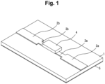
- Fig. 1 is a perspective view of a DC block structure according to a first embodiment of the present invention
- Fig. 2A is a plan view of the DC block structure
- Fig. 2B is a sectional view of the DC block structure.
- the characteristic impedance of the transmission line 3b is the same as the characteristic impedance of the transmission line 3a.
- the capacitor 4 is a silicon capacitor.
- the capacitor 4 has a structure in which a thin film capacitor 41 is formed on a silicon substrate 40. Further, bumps 42a and 42b are formed so as to be connected with an electrode of the thin film capacitor 41.
- the one bump 42a of the capacitor 4 is electrically connected with the transmission line 3a, and the other bump 42b is electrically connected with the transmission line 3b. In this way, the capacitor 4 is flip-chip mounted on the transmission lines 3a and 3b, and the transmission line 3a and the transmission line 3b are connected in series via the capacitor 4.
- portions of the bumps 42a and 42b of the capacitor 4 function as low-pass filters, but it is possible to impart a peaking characteristic to a frequency characteristic by inductivity of the transmission lines 3a and 3b.
- a roll-off characteristic due to the function of the low-pass filters can be reduced, and the frequency characteristic of the DC block structure can be improved.
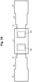
- Fig. 3A is a plan view of a DC block structure according to a second embodiment of the present invention
- Fig. 3B is a sectional view of the DC block structure.
- the same components as those of the first embodiment are denoted by the same reference numerals.
- the DC block structure of the present embodiment includes the dielectric 1, the transmission lines 2a, 2b, 3a, and 3b, the capacitor 4, the ground conductor 5, a transmission line 6a formed on the surface of the dielectric 1 so as to be inserted between the transmission line 2a and the transmission line 3a and designed so that characteristic impedance has a value between the characteristic impedance of the transmission line 2a and the characteristic impedance of the transmission line 3a, and a transmission line 6b formed on the surface of the dielectric 1 so as to be inserted between the transmission line 2b and the transmission line 3b and designed so that characteristic impedance has a value between the characteristic impedance of the transmission line 2b and the characteristic impedance of the transmission line 3b.
- the characteristic impedance of the transmission line 6b is the same as the characteristic impedance of the transmission line 6a.
- a plurality of peaking frequencies can be generated in a frequency characteristic of the DC block structure, and the frequency characteristic can be made flat.
- Fig. 5A is a plan view of a DC block structure according to a third embodiment of the present invention
- Fig. 5B is a sectional view of the DC block structure.
- the same components as those of the first embodiment are denoted by the same reference numerals.
- the DC block structure of the present embodiment includes the dielectric 1, the transmission lines 2a, 2b, 3a, and 3b, the capacitor 4, the ground conductor 5, a transmission line 7a formed on the surface of the dielectric 1 so as to be inserted between the transmission line 2a and the transmission line 3a and designed so that characteristic impedance has a value between the characteristic impedance of the transmission line 2a and the characteristic impedance of the transmission line 3a, and a transmission line 7b formed on the surface of the dielectric 1 so as to be inserted between the transmission line 2b and the transmission line 3b and designed so that characteristic impedance has a value between the characteristic impedance of the transmission line 2b and the characteristic impedance of the transmission line 3b.
- the transmission line 7a is a transmission line having a tapered shape in plan view in which a width gradually changes from a width of the transmission line 2a to a width of the transmission line 3a.
- the transmission line 7b is a transmission line having a tapered shape in plan view in which a width gradually changes from a width of the transmission line 2b to a width of the transmission line 3b.
- the characteristic impedance of the transmission line 7b is the same as the characteristic impedance of the transmission line 7a.
- a plurality of peaking frequencies can be generated in a frequency characteristic of the DC block structure, and the frequency characteristic can be made flat.
- the transmission lines 2a, 2b, 3a, 3b, 6a, 6b, 7a, and 7b are microstrip lines.
- the transmission lines 2a, 2b, 3a, 3b, 6a, 6b, 7a, and 7b may be coplanar lines or grounded coplanar lines.
- Fig. 6 is a perspective view illustrating an example in which the transmission lines 2a, 2b, 3a, and 3b in the first embodiment are coplanar lines.
- Ground conductors 8 are formed at positions on both outer sides of the transmission lines 2a, 2b, 3a, and 3b on a dielectric 1 along a propagation direction of a signal propagating through the transmission lines 2a, 2b, 3a, and 3b.
- a DC block structure can be formed even when a ground conductor cannot be formed on the back surface of the dielectric 1, and a degree of freedom in design can be increased.
- Fig. 7 is a perspective view illustrating an example in which the transmission lines 2a, 2b, 3a, and 3b in the first embodiment are grounded coplanar lines.
- the ground conductors 8 are formed at positions on both outer sides of the transmission lines 2a, 2b, 3a, and 3b on the dielectric 1 along the propagation direction of the signal propagating through the transmission lines 2a, 2b, 3a, and 3b, and the ground conductor 5 is formed on the back surface of the dielectric 1.
- Figs. 6 and 7 the configuration in which the coplanar lines or the grounded coplanar lines are applied to the first embodiment is illustrated, but it is needless to say that the configuration may be applied to the second and third embodiments. That is, similarly to Fig. 6 , when the ground conductors 8 are formed on both outer sides of the transmission lines 2a, 2b, 3a, 3b, 6a, and 6b or on both outer sides of the transmission lines 2a, 2b, 3a, 3b, 7a, and 7b, a coplanar line configuration is obtained. Further, when the ground conductor 5 is formed on the back surface of the dielectric 1 as in Fig. 7 , a grounded coplanar line configuration is obtained.
- a height of the bump can be changed depending on mounting conditions and a bump material.
- a combination of the height design of the bump and the line design makes it possible to expect further improvement in a frequency characteristic of the DC block structure.
- the present invention can be applied to a technique of mounting a capacitor on a high frequency line.
Landscapes
- Engineering & Computer Science (AREA)
- Power Engineering (AREA)
- Microelectronics & Electronic Packaging (AREA)
- Manufacturing & Machinery (AREA)
- Waveguide Connection Structure (AREA)
Abstract
Description
- The present invention relates to a DC block structure using a surface mount capacitor.
- In recent years, an amount of data transmitted on a network has been increasing, and a method of improving a data transmission rate to cope with the increase has been researched and developed. A tendency to require high speed is similarly applied to an optical communication system, and broadband is also required for each device constituting a transceiver of the optical communication system.
- A DC block is inserted between a plurality of devices connected in a cascade, and has a function of cutting a DC voltage component superimposed on a signal and transmitting only an AC signal component to the next stage. This function enables each device to be driven with an appropriate bias. In recent years, in optical communication, each device is required to have a very broadband characteristic from a DC vicinity to a vicinity region of 150 GHz. The DC block inserted between these devices is also required to have broadband.
- As the broadband DC block, a silicon capacitor capable of forming an nF order capacitance on a thin film by applying a semiconductor CMOS process has attracted attention. Conventionally, in a frequency region of 100 GHz or less, a multi-layered chip capacitor (MLCC) which is relatively inexpensive and easily available has been used as the DC block.
-
Fig. 8A is a front view of an MLCC, andFig. 8B is a sectional view of the MLCC. An MLCC 100 includes twoelectrodes electrode layer 102 and a high dielectric 103 made of ceramics are alternately stacked. However, the MLCC has a problem that parasitic capacitances are likely to occur in theelectrodes -
Fig. 9A is a front view of a silicon capacitor, andFig. 9B is a sectional view of the silicon capacitor. Asilicon capacitor 200 has a structure in which athin film capacitor 202 is formed on asilicon substrate 201. Further,bumps thin film capacitor 202. Since the silicon capacitor is formed with the thin film in capacitance, there is an advantage that the silicon capacitor is close to a structure of a transmission line and characteristic deterioration hardly occurs even in a high frequency range. However, the silicon capacitor has a problem that when a characteristic is further extended to the vicinity of 150 GHz, characteristic deterioration occurs in the vicinity of 125 GHz in a conventional mounting structure, and desired performance cannot be obtained. -
Fig. 10A shows a plan view of a conventional DC block structure using a silicon capacitor, andFig. 10B shows a sectional view of the DC block structure. In the conventional DC block structure, thesilicon capacitor 200 is inserted between atransmission line 204a and atransmission line 204b. Thetransmission lines ground conductor 206 is formed on a back surface of the dielectric 205. Thesilicon capacitor 200 is connected with thetransmission lines bumps - The inventors have found that in a case of the conventional DC block structure, there is a problem that a roll-off characteristic in which an insertion loss increases at a frequency of 150 GHz or less occurs. An equivalent circuit of a portion of the
bump 203a indicated by abroken line 207 inFig. 10B is as shown inFig. 11 . InFig. 11 , L represents an inductive component, C1 represents a capacitive component generated on thesilicon capacitor 200 side, and C2 represents a capacitive component generated on thetransmission line 204a side. The reason why the roll-off characteristic is generated at the frequency of 150 GHz or less is that portions of thebumps - Non Patent Literature 1: C. Bunel, et al., "Ultra thin low ESL and ultra wide broadband silicon capacitors", proceedings of 2016 International Conference on Electronics Packaging (ICEP), 2016
- The present invention has been made to solve the above problems, and an object thereof is to provide a broadband DC block structure having an improved frequency characteristic as compared with a conventional DC block structure.
- A DC block structure according to the present invention includes: a dielectric; a first transmission line formed on a surface of the dielectric; a second transmission line formed on the surface of the dielectric and designed so that characteristic impedance is the same as characteristic impedance of the first transmission line; a third transmission line formed on the surface of the dielectric so as to be connected with the first transmission line and designed so that characteristic impedance is higher than the characteristic impedance of the first and second transmission lines; a fourth transmission line formed on the surface of the dielectric so as to be connected with the second transmission line and designed so that characteristic impedance is higher than the characteristic impedance of the first and second transmission lines; and a capacitor mounted on the third and fourth transmission lines so as to connect the third transmission line and the fourth transmission line in series.
- According to the present invention, by providing the third and fourth transmission lines, a frequency characteristic of the DC block structure can have a peaking characteristic. Therefore, it is possible to reduce a roll-off characteristic caused by connection portions between the capacitor and the transmission lines and improve the frequency characteristic of the DC block structure.
-
-
Fig. 1 is a perspective view of a DC block structure according to a first embodiment of the present invention. -
Fig. 2A is a plan view of the DC block structure according to the first embodiment of the present invention. -
Fig. 2B is a sectional view of the DC block structure according to the first embodiment of the present invention. -
Fig. 3A is a plan view of a DC block structure according to a second embodiment of the present invention. -
Fig. 3B is a sectional view of the DC block structure according to the second embodiment of the present invention. -
Fig. 4 is a diagram illustrating simulation results of frequency characteristics of a conventional DC block structure and the DC block structure according to the second embodiment of the present invention. -
Fig. 5A is a plan view of a DC block structure according to a third embodiment of the present invention. -
Fig. 5B is a sectional view of the DC block structure according to the third embodiment of the present invention. -
Fig. 6 is a perspective view of a DC block structure according to a fourth embodiment of the present invention. -
Fig. 7 is a perspective view illustrating another example of the DC block structure according to the fourth embodiment of the present invention. -
Fig. 8A is a front view of an MLCC. -
Fig. 8B is a sectional view of the MLCC. -
Fig. 9A is a front view of a silicon capacitor. -
Fig. 9B is a sectional view of the silicon capacitor. -
Fig. 10A is a plan view of a conventional DC block structure. -
Fig. 10B is a sectional view of the conventional DC block structure. -
Fig. 11 is an equivalent circuit diagram of the conventional DC block structure. - Hereinafter, embodiments of the present invention will be described with reference to the drawings.
Fig. 1 is a perspective view of a DC block structure according to a first embodiment of the present invention,Fig. 2A is a plan view of the DC block structure, andFig. 2B is a sectional view of the DC block structure. The DC block structure of the present embodiment includes a dielectric 1,transmission lines transmission line 3a formed on the surface of the dielectric 1 so as to be connected with thetransmission line 2a and designed so that characteristic impedance is higher than the characteristic impedance of thetransmission lines transmission line 3b formed on the surface of the dielectric 1 so as to be connected with thetransmission line 2b and designed so that characteristic impedance is higher than the characteristic impedance of thetransmission lines capacitor 4 mounted on thetransmission lines transmission lines ground conductor 5 formed on a back surface of thedielectric 1. - The characteristic impedance of the
transmission line 3b is the same as the characteristic impedance of thetransmission line 3a. Similar to a conventional DC block structure, thecapacitor 4 is a silicon capacitor. Thecapacitor 4 has a structure in which athin film capacitor 41 is formed on asilicon substrate 40. Further, bumps 42a and 42b are formed so as to be connected with an electrode of thethin film capacitor 41. The onebump 42a of thecapacitor 4 is electrically connected with thetransmission line 3a, and theother bump 42b is electrically connected with thetransmission line 3b. In this way, thecapacitor 4 is flip-chip mounted on thetransmission lines transmission line 3a and thetransmission line 3b are connected in series via thecapacitor 4. - Also in the present embodiment, portions of the
bumps capacitor 4 function as low-pass filters, but it is possible to impart a peaking characteristic to a frequency characteristic by inductivity of thetransmission lines - Next, a second example of the present invention will be described.
Fig. 3A is a plan view of a DC block structure according to a second embodiment of the present invention, andFig. 3B is a sectional view of the DC block structure. The same components as those of the first embodiment are denoted by the same reference numerals. The DC block structure of the present embodiment includes the dielectric 1, thetransmission lines capacitor 4, theground conductor 5, atransmission line 6a formed on the surface of the dielectric 1 so as to be inserted between thetransmission line 2a and thetransmission line 3a and designed so that characteristic impedance has a value between the characteristic impedance of thetransmission line 2a and the characteristic impedance of thetransmission line 3a, and atransmission line 6b formed on the surface of the dielectric 1 so as to be inserted between thetransmission line 2b and thetransmission line 3b and designed so that characteristic impedance has a value between the characteristic impedance of thetransmission line 2b and the characteristic impedance of thetransmission line 3b. - The characteristic impedance of the
transmission line 6b is the same as the characteristic impedance of thetransmission line 6a. In the present embodiment, by connecting thetransmission line 2a and thetransmission line 3a via thetransmission line 6a and connecting thetransmission line 2b and thetransmission line 3b via thetransmission line 6b, a plurality of peaking frequencies can be generated in a frequency characteristic of the DC block structure, and the frequency characteristic can be made flat. -
Fig. 4 is a diagram illustrating simulation results of frequency characteristics of the conventional DC block structure and the DC block structure of the present embodiment. InFig. 4 ,reference numeral 400 denotes the frequency characteristic of the conventional DC block structure, andreference numeral 401 denotes the frequency characteristic of the DC block structure of the present embodiment. According to the present embodiment, it can be seen that roll-off around 150 GHz which has occurred in the conventional DC block structure is greatly improved. - Next, a third embodiment of the present invention will be described.
Fig. 5A is a plan view of a DC block structure according to a third embodiment of the present invention, andFig. 5B is a sectional view of the DC block structure. The same components as those of the first embodiment are denoted by the same reference numerals. The DC block structure of the present embodiment includes the dielectric 1, thetransmission lines capacitor 4, theground conductor 5, atransmission line 7a formed on the surface of the dielectric 1 so as to be inserted between thetransmission line 2a and thetransmission line 3a and designed so that characteristic impedance has a value between the characteristic impedance of thetransmission line 2a and the characteristic impedance of thetransmission line 3a, and atransmission line 7b formed on the surface of the dielectric 1 so as to be inserted between thetransmission line 2b and thetransmission line 3b and designed so that characteristic impedance has a value between the characteristic impedance of thetransmission line 2b and the characteristic impedance of thetransmission line 3b. - The
transmission line 7a is a transmission line having a tapered shape in plan view in which a width gradually changes from a width of thetransmission line 2a to a width of thetransmission line 3a. Similarly, thetransmission line 7b is a transmission line having a tapered shape in plan view in which a width gradually changes from a width of thetransmission line 2b to a width of thetransmission line 3b. The characteristic impedance of thetransmission line 7b is the same as the characteristic impedance of thetransmission line 7a. - In the present embodiment, by connecting the
transmission line 2a and thetransmission line 3a via thetransmission line 7a and connecting thetransmission line 2b and thetransmission line 3b via thetransmission line 7b, a plurality of peaking frequencies can be generated in a frequency characteristic of the DC block structure, and the frequency characteristic can be made flat. - In the first to third embodiments, a case where the
transmission lines transmission lines -
Fig. 6 is a perspective view illustrating an example in which thetransmission lines Ground conductors 8 are formed at positions on both outer sides of thetransmission lines dielectric 1 along a propagation direction of a signal propagating through thetransmission lines Fig. 6 , a DC block structure can be formed even when a ground conductor cannot be formed on the back surface of the dielectric 1, and a degree of freedom in design can be increased. -
Fig. 7 is a perspective view illustrating an example in which thetransmission lines Fig. 7 , theground conductors 8 are formed at positions on both outer sides of thetransmission lines dielectric 1 along the propagation direction of the signal propagating through thetransmission lines ground conductor 5 is formed on the back surface of thedielectric 1. - In the examples of
Figs. 6 and7 , the configuration in which the coplanar lines or the grounded coplanar lines are applied to the first embodiment is illustrated, but it is needless to say that the configuration may be applied to the second and third embodiments. That is, similarly toFig. 6 , when theground conductors 8 are formed on both outer sides of thetransmission lines transmission lines ground conductor 5 is formed on the back surface of the dielectric 1 as inFig. 7 , a grounded coplanar line configuration is obtained. - In the coplanar line or the grounded coplanar line, characteristic impedance of each transmission line can be designed to a desired value by adjusting an interval between the
transmission lines ground conductor 8. - In the first to fourth embodiments, the
bumps capacitor 4 may be solder bumps formed by a back end process or stud bumps formed using a wire bonder. - In a case of the stud bump, a height of the bump can be changed depending on mounting conditions and a bump material. A combination of the height design of the bump and the line design makes it possible to expect further improvement in a frequency characteristic of the DC block structure.
- The present invention can be applied to a technique of mounting a capacitor on a high frequency line.
-
- 1 Dielectric
- 2a, 2b, 3a, 3b, 6a, 6b, 7a, 7b Transmission line
- 4 Capacitor
- 5, 8 Ground conductor
- 40 Silicon substrate
- 41 Thin film capacitor
- 42a, 42b Bump
Claims (8)
- A DC block structure comprising:a dielectric;a first transmission line formed on a surface of the dielectric;a second transmission line formed on the surface of the dielectric and designed so that characteristic impedance is same as characteristic impedance of the first transmission line;a third transmission line formed on the surface of the dielectric so as to be connected with the first transmission line and designed so that characteristic impedance is higher than the characteristic impedance of the first and second transmission lines;a fourth transmission line formed on the surface of the dielectric so as to be connected with the second transmission line and designed so that characteristic impedance is higher than the characteristic impedance of the first and second transmission lines; anda capacitor mounted on the third and fourth transmission lines so as to connect the third transmission line and the fourth transmission line in series.
- The DC block structure according to claim 1, further comprising:a fifth transmission line formed on the surface of the dielectric so as to be inserted between the first transmission line and the third transmission line and designed so that characteristic impedance has a value between the characteristic impedance of the first transmission line and the characteristic impedance of the third transmission line; anda sixth transmission line formed on the surface of the dielectric so as to be inserted between the second transmission line and the fourth transmission line and designed so that characteristic impedance has a value between the characteristic impedance of the second transmission line and the characteristic impedance of the fourth transmission line.
- The DC block structure according to claim 2, whereinthe fifth transmission line is a transmission line having a tapered shape in plan view in which a width gradually changes from a width of the first transmission line to a width of the third transmission line, andthe sixth transmission line is a transmission line having a tapered shape in plan view in which a width gradually changes from a width of the second transmission line to a width of the fourth transmission line.
- The DC block structure according to any one of claims 1 to 3, further comprising
a ground conductor formed on a back surface of the dielectric. - The DC block structure according to claim 1, further comprising
first ground conductors formed at positions on both outer sides of the first, second, third, and fourth transmission lines on the dielectric. - The DC block structure according to claim 2, further comprising
first ground conductors formed at positions on both outer sides of the first, second, third, fourth, fifth, and sixth transmission lines on the dielectric. - The DC block structure according to claim 5 or 6, further comprising
a second ground conductor formed on a back surface of the dielectric. - The DC block structure according to any one of claims 1 to 3, wherein
the capacitor is a silicon capacitor in which a thin film capacitor is formed on a silicon substrate, and is mounted on the third and fourth transmission lines via bumps.
Applications Claiming Priority (1)
| Application Number | Priority Date | Filing Date | Title |
|---|---|---|---|
| PCT/JP2022/021538 WO2023228352A1 (en) | 2022-05-26 | 2022-05-26 | Dc block structure |
Publications (2)
| Publication Number | Publication Date |
|---|---|
| EP4535554A1 true EP4535554A1 (en) | 2025-04-09 |
| EP4535554A4 EP4535554A4 (en) | 2026-03-11 |
Family
ID=88918727
Family Applications (1)
| Application Number | Title | Priority Date | Filing Date |
|---|---|---|---|
| EP22943754.6A Pending EP4535554A4 (en) | 2022-05-26 | 2022-05-26 | DC block structure |
Country Status (3)
| Country | Link |
|---|---|
| EP (1) | EP4535554A4 (en) |
| JP (1) | JP7754304B2 (en) |
| WO (1) | WO2023228352A1 (en) |
Family Cites Families (8)
| Publication number | Priority date | Publication date | Assignee | Title |
|---|---|---|---|---|
| JPH02237301A (en) * | 1989-03-10 | 1990-09-19 | Nec Corp | Coaxial microstrip line converter |
| JP3496752B2 (en) * | 1998-02-19 | 2004-02-16 | シャープ株式会社 | Microwave / millimeter wave equipment |
| JP2001196849A (en) * | 2000-01-04 | 2001-07-19 | Sharp Corp | Array antenna feed circuit |
| GB2383199B (en) * | 2001-12-11 | 2005-11-16 | Marconi Optical Components Ltd | Transmission line structures |
| US7535321B1 (en) * | 2006-01-17 | 2009-05-19 | Xilinx, Inc. | Method and apparatus for a printed circuit board (PCB) embedded filter |
| EP2117070B1 (en) * | 2007-01-31 | 2016-04-13 | Mitsubishi Electric Corporation | Microwave device, high frequency device and high frequency apparatus |
| US10707547B2 (en) * | 2018-06-26 | 2020-07-07 | Raytheon Company | Biplanar tapered line frequency selective limiter |
| WO2020121676A1 (en) * | 2018-12-14 | 2020-06-18 | ソニーセミコンダクタソリューションズ株式会社 | Transmission path |
-
2022
- 2022-05-26 JP JP2024522822A patent/JP7754304B2/en active Active
- 2022-05-26 WO PCT/JP2022/021538 patent/WO2023228352A1/en not_active Ceased
- 2022-05-26 EP EP22943754.6A patent/EP4535554A4/en active Pending
Also Published As
| Publication number | Publication date |
|---|---|
| EP4535554A4 (en) | 2026-03-11 |
| JPWO2023228352A1 (en) | 2023-11-30 |
| WO2023228352A1 (en) | 2023-11-30 |
| JP7754304B2 (en) | 2025-10-15 |
Similar Documents
| Publication | Publication Date | Title |
|---|---|---|
| US7196598B2 (en) | Dielectric waveguide filter with inductive windows and coplanar line coupling | |
| EP3477693A1 (en) | High-frequency ceramic substrate and high-frequency semiconductor element housing package | |
| US8558645B2 (en) | Apparatus for improving transmission bandwidth | |
| EP0448085A2 (en) | Dielectric filter | |
| US11417615B2 (en) | Transition circuitry for integrated circuit die | |
| JP2003188047A (en) | DC block circuit and communication device | |
| US7046100B2 (en) | Direct current cut structure | |
| EP4535554A1 (en) | Dc block structure | |
| JP2000068713A (en) | Feed through structure of distribution constant line and package substrate using it | |
| JPH11195731A (en) | Semiconductor device | |
| JP2013197435A (en) | Wiring substrate | |
| JP3303226B2 (en) | Flip chip mounting structure | |
| US20230029621A1 (en) | Lc filter, and diplexer and multiplexer using same | |
| US7026869B2 (en) | Broadband amplifier having offset microstrip section in a housing module | |
| JP3395290B2 (en) | High frequency circuit board | |
| JP2002064310A (en) | Microwave / millimeter wave equipment | |
| US6239400B1 (en) | Method and device for connecting two millimeter elements | |
| US20260122768A1 (en) | Wiring board and electronic device | |
| JPH04117702A (en) | Hybrid integrated circuit connector | |
| CN117954817A (en) | High frequency circuits and radar devices | |
| JP2567210B2 (en) | Microwave ground structure | |
| JP4145101B2 (en) | Electronic circuit | |
| EP3879286A1 (en) | Semiconductor die and method for testing an electronic circuit formed in a semiconductor die | |
| JP2001257286A (en) | Millimeter-wave semiconductor device | |
| JP2001177012A (en) | High frequency wiring board |
Legal Events
| Date | Code | Title | Description |
|---|---|---|---|
| STAA | Information on the status of an ep patent application or granted ep patent |
Free format text: STATUS: THE INTERNATIONAL PUBLICATION HAS BEEN MADE |
|
| PUAI | Public reference made under article 153(3) epc to a published international application that has entered the european phase |
Free format text: ORIGINAL CODE: 0009012 |
|
| STAA | Information on the status of an ep patent application or granted ep patent |
Free format text: STATUS: REQUEST FOR EXAMINATION WAS MADE |
|
| 17P | Request for examination filed |
Effective date: 20241125 |
|
| AK | Designated contracting states |
Kind code of ref document: A1 Designated state(s): AL AT BE BG CH CY CZ DE DK EE ES FI FR GB GR HR HU IE IS IT LI LT LU LV MC MK MT NL NO PL PT RO RS SE SI SK SM TR |
|
| DAV | Request for validation of the european patent (deleted) | ||
| DAX | Request for extension of the european patent (deleted) | ||
| RAP3 | Party data changed (applicant data changed or rights of an application transferred) |
Owner name: NTT, INC. |
|
| A4 | Supplementary search report drawn up and despatched |
Effective date: 20260209 |
|
| RIC1 | Information provided on ipc code assigned before grant |
Ipc: H01P 5/02 20060101AFI20260203BHEP Ipc: H01G 2/06 20060101ALI20260203BHEP Ipc: H01G 4/228 20060101ALI20260203BHEP Ipc: H01G 4/30 20060101ALI20260203BHEP Ipc: H01G 4/33 20060101ALI20260203BHEP Ipc: H01G 4/40 20060101ALI20260203BHEP Ipc: H05K 1/181 20260101ALI20260203BHEP Ipc: H10D 1/60 20250101ALI20260203BHEP Ipc: H01P 1/20 20060101ALI20260203BHEP |