EP4530697A2 - Methods of fabrication of compound light-guide optical elements having embedded coupling-in reflectors - Google Patents
Methods of fabrication of compound light-guide optical elements having embedded coupling-in reflectors Download PDFInfo
- Publication number
- EP4530697A2 EP4530697A2 EP25156234.4A EP25156234A EP4530697A2 EP 4530697 A2 EP4530697 A2 EP 4530697A2 EP 25156234 A EP25156234 A EP 25156234A EP 4530697 A2 EP4530697 A2 EP 4530697A2
- Authority
- EP
- European Patent Office
- Prior art keywords
- faces
- parallel
- optical
- pair
- partially reflective
- Prior art date
- Legal status (The legal status is an assumption and is not a legal conclusion. Google has not performed a legal analysis and makes no representation as to the accuracy of the status listed.)
- Pending
Links
Images


Classifications
-
- G—PHYSICS
- G02—OPTICS
- G02B—OPTICAL ELEMENTS, SYSTEMS OR APPARATUS
- G02B6/00—Light guides; Structural details of arrangements comprising light guides and other optical elements, e.g. couplings
- G02B6/10—Light guides; Structural details of arrangements comprising light guides and other optical elements, e.g. couplings of the optical waveguide type
- G02B6/12—Light guides; Structural details of arrangements comprising light guides and other optical elements, e.g. couplings of the optical waveguide type of the integrated circuit kind
- G02B6/13—Integrated optical circuits characterised by the manufacturing method
-
- G—PHYSICS
- G02—OPTICS
- G02B—OPTICAL ELEMENTS, SYSTEMS OR APPARATUS
- G02B27/00—Optical systems or apparatus not provided for by any of the groups G02B1/00 - G02B26/00, G02B30/00
- G02B27/10—Beam splitting or combining systems
- G02B27/14—Beam splitting or combining systems operating by reflection only
- G02B27/145—Beam splitting or combining systems operating by reflection only having sequential partially reflecting surfaces
-
- G—PHYSICS
- G02—OPTICS
- G02B—OPTICAL ELEMENTS, SYSTEMS OR APPARATUS
- G02B27/00—Optical systems or apparatus not provided for by any of the groups G02B1/00 - G02B26/00, G02B30/00
- G02B27/0081—Optical systems or apparatus not provided for by any of the groups G02B1/00 - G02B26/00, G02B30/00 with means for altering, e.g. enlarging, the entrance or exit pupil
-
- G—PHYSICS
- G02—OPTICS
- G02B—OPTICAL ELEMENTS, SYSTEMS OR APPARATUS
- G02B27/00—Optical systems or apparatus not provided for by any of the groups G02B1/00 - G02B26/00, G02B30/00
- G02B27/01—Head-up displays
- G02B27/017—Head mounted
- G02B27/0172—Head mounted characterised by optical features
-
- G—PHYSICS
- G02—OPTICS
- G02B—OPTICAL ELEMENTS, SYSTEMS OR APPARATUS
- G02B6/00—Light guides; Structural details of arrangements comprising light guides and other optical elements, e.g. couplings
- G02B6/0001—Light guides; Structural details of arrangements comprising light guides and other optical elements, e.g. couplings specially adapted for lighting devices or systems
- G02B6/0011—Light guides; Structural details of arrangements comprising light guides and other optical elements, e.g. couplings specially adapted for lighting devices or systems the light guides being planar or of plate-like form
- G02B6/0033—Means for improving the coupling-out of light from the light guide
- G02B6/0035—Means for improving the coupling-out of light from the light guide provided on the surface of the light guide or in the bulk of it
- G02B6/0036—2-D arrangement of prisms, protrusions, indentations or roughened surfaces
-
- G—PHYSICS
- G02—OPTICS
- G02B—OPTICAL ELEMENTS, SYSTEMS OR APPARATUS
- G02B6/00—Light guides; Structural details of arrangements comprising light guides and other optical elements, e.g. couplings
- G02B6/10—Light guides; Structural details of arrangements comprising light guides and other optical elements, e.g. couplings of the optical waveguide type
- G02B6/12—Light guides; Structural details of arrangements comprising light guides and other optical elements, e.g. couplings of the optical waveguide type of the integrated circuit kind
- G02B6/122—Basic optical elements, e.g. light-guiding paths
-
- G—PHYSICS
- G02—OPTICS
- G02B—OPTICAL ELEMENTS, SYSTEMS OR APPARATUS
- G02B6/00—Light guides; Structural details of arrangements comprising light guides and other optical elements, e.g. couplings
- G02B6/24—Coupling light guides
- G02B6/36—Mechanical coupling means
- G02B6/38—Mechanical coupling means having fibre to fibre mating means
- G02B6/3807—Dismountable connectors, i.e. comprising plugs
- G02B6/3833—Details of mounting fibres in ferrules; Assembly methods; Manufacture
- G02B6/3863—Details of mounting fibres in ferrules; Assembly methods; Manufacture fabricated by using polishing techniques
-
- B—PERFORMING OPERATIONS; TRANSPORTING
- B32—LAYERED PRODUCTS
- B32B—LAYERED PRODUCTS, i.e. PRODUCTS BUILT-UP OF STRATA OF FLAT OR NON-FLAT, e.g. CELLULAR OR HONEYCOMB, FORM
- B32B2307/00—Properties of the layers or laminate
- B32B2307/40—Properties of the layers or laminate having particular optical properties
- B32B2307/416—Reflective
-
- B—PERFORMING OPERATIONS; TRANSPORTING
- B32—LAYERED PRODUCTS
- B32B—LAYERED PRODUCTS, i.e. PRODUCTS BUILT-UP OF STRATA OF FLAT OR NON-FLAT, e.g. CELLULAR OR HONEYCOMB, FORM
- B32B2551/00—Optical elements
-
- B—PERFORMING OPERATIONS; TRANSPORTING
- B32—LAYERED PRODUCTS
- B32B—LAYERED PRODUCTS, i.e. PRODUCTS BUILT-UP OF STRATA OF FLAT OR NON-FLAT, e.g. CELLULAR OR HONEYCOMB, FORM
- B32B38/00—Ancillary operations in connection with laminating processes
- B32B38/0004—Cutting, tearing or severing, e.g. bursting; Cutter details
-
- G—PHYSICS
- G02—OPTICS
- G02B—OPTICAL ELEMENTS, SYSTEMS OR APPARATUS
- G02B27/00—Optical systems or apparatus not provided for by any of the groups G02B1/00 - G02B26/00, G02B30/00
- G02B27/01—Head-up displays
- G02B27/0101—Head-up displays characterised by optical features
- G02B2027/0123—Head-up displays characterised by optical features comprising devices increasing the field of view
- G02B2027/0125—Field-of-view increase by wavefront division
-
- G—PHYSICS
- G02—OPTICS
- G02B—OPTICAL ELEMENTS, SYSTEMS OR APPARATUS
- G02B6/00—Light guides; Structural details of arrangements comprising light guides and other optical elements, e.g. couplings
- G02B6/24—Coupling light guides
- G02B6/25—Preparing the ends of light guides for coupling, e.g. cutting
Definitions
- the present invention relates to light-guide optical elements (LOEs), and in particular, methods for manufacturing compound LOEs for two-dimensional aperture expansion having embedded coupling-in reflectors.
- LOEs light-guide optical elements
- Compound LOEs or "two-dimensional expansion waveguides" have been described in various publications by Lumus Ltd (Israel).
- these compound LOEs employ two regions, each of which is a parallel-faced block of transparent material (i.e., light-transmitting material) for facilitating the propagation of light corresponding to a collimated image by internal reflection at major surfaces, and includes a set of mutually-parallel, internal, partially-reflective surfaces (or "facets"), which redirect the collimated image light while achieving expansion of the optical aperture.
- facets mutually-parallel, internal, partially-reflective surfaces
- Embodiments of the present invention provide methods of fabrication of compound LOEs.
- a method of fabricating a compound light-guide optical element comprises: obtaining a stack having a first pair of faces and a plurality of LOEs, each of the LOEs having a pair of major parallel surfaces and a first plurality of mutually parallel partially reflective internal surfaces oblique to the pair of major parallel surfaces; obtaining a first optical block having a second pair of faces and a second plurality of mutually parallel partially reflective internal surfaces; bonding together the first optical block and the stack such that one of the faces of the first pair of faces is joined to one of the faces of the second pair of faces and such that the first plurality of partially reflective internal surfaces is non-parallel to the second plurality of partially reflective internal surfaces, thereby forming a second optical block; cutting the second optical block along a cutting plane that passes through the other one of the faces of the second pair of faces, thereby forming a first optical structure having an interfacing surface at the cutting plane; obtaining a third optical block
- the method further comprises: for each sliced-out compound LOE, polishing external surfaces of the sliced-out compound LOE formed by cutting the optical structure along two consecutive of the cutting planes.
- the first optical block has a pair of parallel faces
- the second plurality of partially reflective internal surfaces are oblique to the pair of parallel faces of the first optical block.
- the first optical block has a third plurality of mutually parallel partially reflective internal surfaces non-parallel to the first and second pluralities of partially reflective internal surfaces.
- the first optical block has a first region that includes the second plurality of partially reflective internal surfaces and a second region that includes the third plurality of partially reflective internal surfaces, the first and second regions of the first optical block are non-overlapping regions.
- the third plurality of partially reflective internal surfaces are parallel to the major parallel surfaces of the LOEs.
- each respective one of the third partially reflective internal surfaces is located in a plane that is approximately halfway between the pair of major parallel surfaces of a respective one of the LOEs.
- the third plurality of partially reflective internal surfaces is located between the first and second pluralities of partially reflective internal surfaces.
- the second plurality of partially reflective internal surfaces is located between the first and third pluralities of partially reflective internal surfaces.
- the first optical block is formed by bonding together first and second constituent optical blocks that each have a pair of faces such that one of the faces of the pair of faces of the first constituent optical block is joined to one of the faces of the pair of faces of the second constituent optical block, the first constituent optical block includes the second plurality of partially reflective internal surfaces, and the second constituent optical block includes a third plurality of mutually parallel partially reflective internal surfaces non-parallel to the first plurality of partially reflective internal surfaces and non-parallel to the second plurality of partially reflective internal surfaces.
- the third optical block and the first optical structure are bonded together such that substantially the entirety of the one of the faces of the third pair of faces is joined to substantially the entirety of the interfacing surface.
- the third optical block and the first optical structure are bonded together such that the one of the faces of the third pair of faces is joined to a fractional portion of the interfacing surface.
- the third optical block has an additional pair of faces
- the method further comprises: obtaining a second inert block having a pair of faces; and bonding together the second inert block and the compound block such that one of the faces of the pair of faces of the second inert block is joined to the second face of the compound block.
- bonding together the third optical block and the first optical structure includes: bonding together the compound block and the first optical structure such that the first face of the compound block is joined to the interfacing surface.
- the method further comprises: obtaining an inert block having a pair of faces; and bonding together the inert block and the third optical block such that one of the faces of the pair of faces of the second inert block is joined to the other one of the faces of the third pair of faces of the optical block.
- the stack is a bonded stack of the LOEs and a plurality of transparent spacer plates, the LOEs and the transparent spacer plates alternate along a length of the stack perpendicular to the major parallel surfaces of the LOEs.
- the at least two cutting planes are located in consecutive spacer plates having one of the LOEs therebetween.
- the first optical block further includes an additional pair of faces, one of major parallel surfaces of the LOE at a top end of the stack forms part of one of the faces of the additional pair of faces, and one of major parallel surfaces of the LOE at a bottom end of the stack forms part of the other one of the faces of the additional pair of faces.
- the second optical sub-block includes a first sub-block region and a second sub-block region, the second plurality of partially reflective internal surfaces are located in the first sub-block region, a third plurality of mutually parallel partially reflective internal surfaces are located in the second sub-block region, and the third plurality of partially reflective internal surfaces are non-parallel to the first plurality of partially reflective internal surfaces and non-parallel to the second plurality of partially reflective internal surfaces.
- the second plurality of partially reflective internal surfaces is located between the first and third pluralities of partially reflective internal surfaces.
- a method of fabricating a compound light-guide optical element comprises: obtaining a first optical block having a first pair of faces and a first plurality of mutually parallel partially reflective internal surfaces; obtaining a second optical block formed as a stack of LOEs and having a second pair of faces, each of the LOEs having a pair of major parallel surfaces and a second plurality of mutually parallel partially reflective internal surfaces oblique to the pair of major parallel surfaces; obtaining a third optical block having a third pair of faces and a third plurality of mutually parallel partially reflective internal surfaces; bonding together the first and third optical blocks and bonding together the second and third optical blocks to form a fourth optical block, the bonding is such that: i) one of the faces of the first pair of faces is joined to one of the faces of the third pair of faces, ii) one of the faces of the second pair of faces is joined to the other one of the faces of the third pair of faces, ii
- the stack is a bonded stack of the LOEs and a plurality of transparent spacer plates, the LOEs and the transparent spacer plates alternate along a length of the stack perpendicular to the major parallel surfaces of the LOEs.
- the at least two cutting planes are located in consecutive spacer plates having one of the LOEs therebetween.
- a method of fabricating a compound light-guide optical element comprises: obtaining a first optical block having a first pair of faces and a first plurality of mutually parallel partially reflective internal surfaces; obtaining a second optical block formed as a stack of LOEs and having a second pair of faces, each of the LOEs having a pair of major parallel surfaces and a second plurality of mutually parallel partially reflective internal surfaces oblique to the pair of major parallel surfaces; obtaining a third optical block having a third pair of faces and a third plurality of mutually parallel partially reflective internal surfaces; bonding together the first and third optical blocks and bonding together the first and second optical blocks to form a fourth optical block, the bonding is such that: i) one of the faces of the third pair of faces is joined to one of the faces of the first pair of faces, ii) one of the faces of the second pair of faces is joined to the other one of the faces of the first pair of faces, ii
- the stack is a bonded stack of the LOEs and a plurality of transparent spacer plates, the LOEs and the transparent spacer plates alternate along a length of the stack perpendicular to the major parallel surfaces of the LOEs.
- the at least two cutting planes are located in consecutive spacer plates having one of the LOEs therebetween.
- Embodiments of the present invention provide methods of fabrication of compound LOEs.
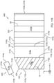
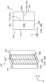
- FIGS. 1A - 1C illustrate various views of a compound LOE 1.
- the compound LOE 1 includes a first LOE 10 and a second LOE 20 that are bonded together at an interface 40.
- the two LOEs 10, 20 are manufactured separately and bonded together.
- the term "bonded” or “bonding” should be understood to mean attached or attaching with an optical cement or glue, or any other suitable adhesive.
- the first LOE 10 is formed from a light-transmitting material and includes a first pair of faces 12a , 12 b (which may or may not be parallel faces), a second pair of faces (major external surfaces) 14 a, 14 b that is a pair of parallel faces, a third pair of faces (major external surfaces) 16 a, 16 b (that may or may not be parallel faces), and a plurality of mutually parallel partially reflective internal surfaces (also referred to as "facets") 18 that at least partially traverse the LOE 10 between the faces 16 a, 16 b.
- the LOE 10 is configured to guide light (image illumination), corresponding to a collimated image injected into the LOE 10 by an image projector (not shown), such that the light (represented in FIG.
- the LOE 10 is further configured to gradually couple the propagating (trapped) light out of the LOE 10 via the facets 18, which are inclined obliquely to the direction of propagation of the light and each reflect a proportion of the intensity of the propagating light, thereby expanding the image illumination in one dimension (which in this case is approximately along the y-axis).
- the light coupled out of the LOE 10 by the facets 18 is represented by light rays 60 ( FIGS. 1A and 1B ), and the propagation of the collimated image light 50 by internal reflection at the faces of the LOE 10 is represented by left-going and right-going rays 52 ( FIG. 1A ).
- the facets 18 have a first orientation in the compound LOE 1.
- the facets 18 are obliquely angled relative to faces 14 a, 14 b.
- the facets 18 are orthogonal to the faces 14 a, 14 b.
- the facets 18 can be obliquely angled to one or both of the faces 12 a, 12 b, whereas in other embodiments the facets 18 can be orthogonal to one or both of the faces 12 a, 12 b.
- the faces 12 a, 12 b are parallel, and the facets 18 are inclined obliquely to the faces 12 a, 12 b.
- the reflectivity of the facets 18 can be provided via coatings on the internal surfaces prior to forming the LOE 10.
- the reflectance of each of the facets 18 may be the same, or the reflectivity of the facets 18 may be different from one another and may increase along a light propagation direction (which in the arbitrarily labeled xyz coordinate system in the drawings is along the y-axis).
- the light that is coupled out of the LOE 10 is coupled into the second LOE 20.
- the LOE 20 is also formed from a light-transmitting material and includes a first pair of faces 22 a, 22 b (which may or may not be parallel faces), a second pair of faces (major external surfaces) 24 a, 24 b that is a pair of parallel faces, a third pair of faces (major external surfaces) 26 a, 26 b (that may or may not be parallel faces), and a plurality of mutually parallel partially reflective internal surfaces ("facets") 28 that are inclined obliquely relative to faces 24 a, 24 b.
- the faces 14 a, 24 a are generally coincident (coplanar) so as to form a first singular external face of the compound LOE 1.
- the faces 14 b, 24 b are generally coincident (coplanar) so as to form a second singular external face of the compound LOE 1.
- the faces 16 a, 26 a are also preferably generally coincident (coplanar) so as to form a third singular external face of the compound LOE 1, and the faces 16 b, 26 b are also preferably generally coincident (coplanar) so as to form a fourth singular external face of the compound LOE 1.
- the remaining two external surfaces of the compound LOE 1 are respectively formed from the faces 12 a and 22 b.
- the facets 28 have a second orientation in the compound LOE 1 that is non-parallel to the first orientation of the facets 18.
- the reflectivity of the facets 28 can be provided via coatings on the internal surfaces prior to forming the LOE 20.
- the reflectance of each of the facets 28 may be the same, or the reflectivity of the facets 28 may be different from one another and may increase along a light propagation direction (which in the arbitrarily labeled xyz coordinate system in the drawings is along the x-axis).
- the light from LOE 10 is coupled into the LOE 20 through interface 40 (which is coincident with the face 12 b and the face 22 a).
- the LOE 20 is configured to guide the light by internal reflection (preferably but not exclusively total internal reflection) at the faces 24 a, 24 b, and to gradually couple the propagating light out of the LOE 20 via the facets 28, which each reflect a proportion of the intensity of the propagating light, toward the eye of an observer, thereby expanding the image illumination in a second dimension (which in this case is along the x-axis).
- the propagation of image light through the LOE 20 by internal reflection at faces 24 a, 24 b is represented by sets of rays 62, 63.
- One of the rays 62, 63 represents the image and the other of the rays 62, 63 represents the image conjugate corresponding to the light 60 that coupled into the LOE 20 from the LOE 10.
- the light coupled out of the LOE 20 by the facets 28 is represented in FIG. 1A by light rays 64.
- the image illumination that is to be coupled into the compound LOE 1 for guiding by the LOE 10 and the LOE 20 is generated by an external image projector (not shown), which is typically implemented as a micro-projector arrangement formed from a microdisplay device (such as an LCoS chip) that generates image illumination, and collimating optics for collimating the image illumination to produce collimated image illumination.
- the collimated image illumination is coupled into the LOE 10 by a coupling-in optical arrangement, in the form of a highly reflective internal surface 42 in a coupling-in region of the LOE 10.
- FIGS. 2A and 2B illustrate a compound LOE having such an additional facet 38.
- the facet 38 can be deployed in part of the LOE 10, or as shown in FIGS. 2A and 2B as part of a separate light-transmitting substrate 30 having three pairs of faces 32a, 32b, 34a, 34b, 36a, 36b (where the pair of faces 34a, 34b is a pair of parallel faces).
- the facet 38 is parallel to the faces 14a, 14b, 24a, 24b, and thus has an orientation that is non-parallel to the orientations of the facets 18, 28.
- the facet 38 is preferably located halfway between faces 24 a, 24 b (and equivalently halfway between faces 14 a, 14 b). If using more than one facet 38, the facets 38 are preferably evenly spaced between faces 24 a, 24 b. In the embodiment illustrated in FIGS.
- the LOE 10 and the substrate 30 are bonded together at faces 12 b, 32 a, and the substrate 30 and the LOE 20 are bonded together at faces 22 a, 32 b, such that the facet 38 is located between the sets of facets 18, 28. It is noted however that other deployments are also possible, for example in which the facets 18 are located between the facet 38 and the set of facets 28, depending on the design specification of the specific application for the compound LOE.
- the light 60 (coupled-out by facets 18) is partially reflected by the facet 38.
- the reflected and transmitted parts of light 60 are coupled into the LOE 20, and correspond to rays 62 and 63, respectively.
- compound LOEs including compound LOEs that may be similar to the compound LOEs illustrated in FIGS. 1A - 2B , can be found in various publications by Lumus Ltd. (Israel), including, for example, US Patent Application Publication No. 2021/0247608 , PCT publication WO 2021/240513 , PCT publication WO 2021/152602 , PCT publication WO 2021/001841 , and US Patent No. 10,551,544 .
- Embodiments of the present invention are directed to methods of fabricating compound LOEs.
- the compound LOEs that are fabricated according to the methods of the present invention may be different in structure from the compound LOEs illustrated in FIGS. 1A - 2B , but have similar components, as will become apparent from the ensuing description.
- the fabrication method steps are described in detail below with reference to FIGS. 3A - 21 , and generally include steps of obtaining an optical block 400 ( FIGS.
- FIGS. 7A - 7C having sets of the requisite facets 18, 28 (and preferably also a set of facets 38) embedded in regions of the optical block 400 and appropriately oriented relative to each other such that the facets 18, 28 (and 38) are mutually non-parallel, cutting a portion of the optical block 400 at a prescribed cutting plane ( FIGS. 8A and 8B ) that is at a prescribed angle and passes through particular faces of the optical block 400 to form an optical structure 400' having an interfacing surface ( FIGS. 9A and 9B ) formed at the cutting plane, obtaining an additional optical block 500 ( FIGS.
- FIGS. 12A and 12B having embedded therein sets of the requisite facets 18, 28 (and preferably also a set of facets 38) and a set of the reflective internal surfaces 42 that is non-parallel to the facets 18, 28, 38.
- the intermediate optical structure 600 is then cut along two or more cutting planes in order to slice-out one or more compound LOEs ( FIGS. 13 - 14B ), where each compound LOE has facets 18 and facets 28 (and preferably also at least one facet 38) and an embedded reflective internal surface 42.
- Each of the sliced-out compound LOEs can then be polished to achieve a final compound LOE having a desired thickness ( FIG. 15 ).
- one or more blocks 800, 900 of inert material are bonded to the optical block 500 to form a compound block 590 ( FIGS. 16A - 18B ), which is then bonded to the optical structure 400' ( FIGS. 19A and 19B ) to form the intermediate optical structure 600.
- obtaining the optical block 400 can include producing the optical block 400 by obtaining various other optical blocks 100, 200, 300 ( FIGS. 3A - 5C ) and bonding those optical blocks 100, 200, 300 together to form the optical block 400.
- Each of the optical blocks 100, 200, 300 has one of the requisite sets of facets 18, 28, 38 embedded therein, and can be produced from sets of bonded coated plates that are cut at appropriate angles and thickness.
- each of the various blocks 100, 200, 300, 400, 500, 800, 900 is represented as a rectangular cuboid, i.e., a structure having three pairs of parallel faces that are mutually perpendicular (orthogonal).
- rectangular cuboids i.e., a structure having three pairs of parallel faces that are mutually perpendicular (orthogonal).
- parallelism and perpendicularity among all of the faces of the individual blocks is not a strict requirement from an optical standpoint or a manufacturing standpoint.
- only one pair of faces of a block need be a pair of parallel faces, and the remaining faces may or may not be parallel.
- none of the faces of a block need be a pair of parallel faces.
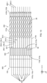
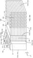
- FIG. 3A there is shown the optical block 200, which is formed as a stack of LOEs 20 that are bonded together.
- the optical block 200 has at least two pairs of faces (major external surfaces), namely a pair of preferably parallel faces 212 a, 212 b, and a pair of faces 214 a, 214 b that is a pair of parallel faces and may be orthogonal (perpendicular) to either or both the faces 212 a , 212 b .
- the optical block 200 also includes a third pair of faces that may or may not be a pair of parallel faces, and may also be perpendicular to one or more of the faces 212 a , 212 b , 214 a , 214 b .
- the third pair of faces are not shown in FIG. 3A , but are shown in various other drawings, including FIGS. 6B , 7B , 8B , 9B , 11B , 12B , and 19B .
- the faces 214 a and 214 b can respectively form part of upper and lower face of the optical structure 600 (FIGS. 11C and 11D) from which a compound LOE can be sliced-out.
- each of the LOEs 20 in the stack of FIG. 3A is an LOE as illustrated in FIG. 3B .
- This LOE 20 is also generally similar to the second LOE 20 discussed above with reference to FIGS. 1A - 2C.
- each LOE 20 is formed from a light-transmitting material having parallel faces 24 a , 24 b and a set (plurality) of internal facets 28 inclined obliquely to the faces 24 a , 24 b .
- Such an LOE can be used as a standalone LOE (together with appropriate coupling-in optics) in situations in which aperture expansion in only one-dimension is desired.
- LOE This type of LOE is commonly referred to as a "one-dimensional" LOE, and the structure and methods of manufacturing such one-dimensional LOEs have been described extensively in various publications by Lumus Ltd. (Israel), including, for example, US Patent No. 7,634,214 , US Patent No. 8,873,150 , PCT publication WO 2016/103263 , and PCT publication WO 2020/212835 .
- FIG. 3C shows one example method of fabricating a plurality of LOEs 20, which can be used to produce the optical block 200.
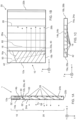
- a plurality of light-transmitting plates is coated to form coated plates 202 which are stacked and bonded together, and then cut along equally spaced parallel cutting planes 206 (which in the arbitrarily labeled xyz coordinate system are parallel to the xy plane).
- Each of the plates 202 has a pair of parallel faces (surfaces) 204 a, 204 b which are appropriately coated with coatings that provide the reflectivity of the facets 28 (such that the facets 28 are partially reflective).
- the cutting planes 206 are oblique to the faces 204 a, 204 b and define the oblique angle of the facets 28, and the resulting cuts along the cutting planes 206 define the faces 24 a, 24 b of the LOEs 20.
- the cutting planes 206 are spaced at predetermined intervals. Preferably the predetermined intervals are uniform intervals such that the cutting planes 206 are uniformly spaced.
- the uniform spacing is preferably in the range of 1 - 2 millimeters, such that the thickness of each LOE 20 (measured between faces 24 a, 24 b) is approximately 1 - 2 millimeters.
- the LOEs 20 Prior to bonding together the LOEs 20 to form the optical block 200, the LOEs 20 are first aligned and arranged in a formation 210 ( FIG. 3D ). The LOEs 20 in the formation 210 are then bonded together to form the optical block 200 ( FIG. 3A ) as a bonded stack of LOEs 20, such that the faces 24 a and 24 b of adjacent (consecutive) LOEs 20 are joined together at bonding regions, and such that the sets of internal facets 28 of the LOEs 20 constitute a plurality of facets 28 of the optical block 200. As can be seen from FIGS.
- the major surface 24 a of the LOE 20 at the top end of the stack 200 forms the top face 214 a of the stack 200
- the major surface 24 b of the LOE 20 at the bottom end of the stack 200 forms the bottom face 214 b of the stack 200.
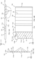
- the optical block 100 is formed from a light-transmitting material and has an embedded set of the facets 18.
- the optical block 100 includes three pairs of faces (major external surfaces), namely a pair of faces 112 a, 112 b (which may or may not be parallel faces), a pair of preferably parallel faces 114 a, 114 b, and a pair of faces 116 a, 116 b (which may or may not be parallel faces).
- the pairs of faces of the optical block 100 are mutually orthogonal (perpendicular), which can simplify the fabrication process.
- the optical block 100 can be formed from a plurality of bonded, transparent coated plates 102 (each plate being formed from a light-transmitting material and coated with a partially reflective coating) to form facets 18 that are angled relative to the faces 114 a, 114 at a predetermined angle, i.e., the facets 18 may be inclined obliquely relative to the faces 114 a, 114 b or may be orthogonal to the faces 114 a, 114 b. The facets 18 may also be inclined obliquely to the faces 112 a, 112 b at a predetermined angle.
- Various known methods exist for forming the optical block 100 are known methods exist for forming the optical block 100. FIG.
- 4C illustrates one such method, in which the coated plates 102 are stacked and bonded together (similar to as in FIG. 3C ), and then cut along a first pair of preferably parallel cutting planes 104 and along a second pair of preferably parallel cutting planes 106 that are preferably perpendicular to the planes 104, in order to extract the optical block 100.
- the angle of the cutting planes 104 relative to the faces of the coated plates 102 determines the angle at which the facets 18 are inclined relative to faces 112 a, 112 b.
- the cuts along the cutting planes 104 define the faces 112 a, 112 b of the optical block 100
- the cuts along cutting planes 106 define the faces 116 a, 116 b of the optical block 100.
- the cutting planes 104, 106 are perpendicular to the thickness dimension of the plates 102 such that the resultant facets 18 are perpendicular to the faces 114 a, 114 b of the optical block 100.
- the cutting planes 104, 106 are perpendicular to the thickness dimension of the plates 102
- the cutting planes 104 are parallel to the yz plane and the cutting planes 106 are parallel to the xz plane.
- the cutting planes 106 are perpendicular to the planes 104.
- the facets 18 are inclined obliquely to the faces 114 a, 114 b, and as such the cutting planes 106 may be inclined at an appropriate oblique angle relative to the xz plane to produce the appropriate facet angle relative to the faces 114 a, 114 b.
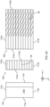
- the optical block 300 is formed from a light-transmitting material and has an embedded set of the facets 38.
- the optical block 300 includes three pairs of faces (major external surfaces), namely a pair of faces 312 a, 312 b (which may or may not be parallel faces), a pair of preferably parallel faces 314 a, 314 b, and a pair of faces 316 a, 316 b (which may or may not be parallel faces).
- the pairs of faces of the optical block 100 are mutually orthogonal (perpendicular).
- the optical block 300 can be formed from a plurality of bonded, transparent coated plates 302 (each plate being a formed from a light-transmitting material and coated with a partially reflective coating) to form facets 38 that are parallel to faces 314 a, 314 b and optionally perpendicular to one or both faces 312 a, 312 b.
- FIG. 5C illustrates one such method, in which the coated plates 302 are stacked and bonded (similar to as in FIGS. 3C and 4C ), and then cut along a pair of cutting planes 304 in order to extract the optical block 100.
- FIG. 5C illustrates one such method, in which the coated plates 302 are stacked and bonded (similar to as in FIGS. 3C and 4C ), and then cut along a pair of cutting planes 304 in order to extract the optical block 100.
- FIG. 5C illustrates one such method, in which the coated plates 302 are stacked and bonded (similar to as in FIGS. 3C and 4C ), and then
- the planes 304 are parallel planes (which in the arbitrarily labeled xyz coordinate system are parallel to the yz plane). However, as alluded to above, parallelism between the planes 304 is not a strict requirement, and in certain cases it may be advantageous to cut along non-parallel cutting planes, which can improve compactness and overall form factor of the final compound LOE product.
- the planes 304 are perpendicular to the major external surfaces (faces) of the plates 202. However, this perpendicularity is also not an optical requirement for producing the final compound LOE product, but is rather a matter of practical convenience when fabricating the compound LOE.
- the stacked and bonded plates may also be cut along an additional pair of cutting planes 306 that pass through two of the plates, and may be parallel to the major external surfaces of the plates 202 and perpendicular to planes 304.
- the cutting planes 306 are parallel to the xy plane.
- FIGS. 6A - 6C show the three optical blocks 100, 200, 300 prior to being bonded together to form the optical block 400 ( FIGS. 7A - 7C ).
- the optical blocks 100, 200, 300 Prior to bonding, it is important that the optical blocks 100, 200, 300 are appropriately aligned such that the orientation of the facets 18 is non-parallel to the orientation of the facets 28, and such that the orientation of the facets 38 is non-parallel to the orientations of the facets 18, 28.
- the blocks 100, 200, 300 are aligned such that the facets 18, 28, 38 are mutually non-parallel.
- the optical block 300 is aligned with the optical block 200 such that the facets 38 of optical block 300 are in planes that are parallel to the planes of faces 214 a, 214 b of the optical block 200.
- the optical blocks 200 and 300 are preferably aligned such that each respective facet 38 is located in a plane that is approximately halfway between the major external surfaces 24 a, 24 b of a respective one of the LOEs 20 that forms the optical block 200.
- each compound LOE is to have multiple facets 38 (say N facets 38)
- the optical blocks 200 and 300 are preferably aligned such for each set of N facets 38, the N facets 38 are evenly spaced between the major external surfaces 24 a, 24 b of a respective one of the LOEs 20 that forms the optical block 200.
- the block 300 can be positioned relative to the block 200 without applying too much scrutiny with respect to the positioning of the facets 38 relative to the major external surfaces 24 a, 24 b, and that any mispositioning of the facets 38 relative to the major external surfaces 24 a, 24 b in a sliced-out compound LOE can be corrected (typically by polishing or grinding) at the final stages of fabrication if there are enough spare regions in the sliced-out compound LOE.
- each of the faces 112 a, 212 a, 312 a is in a plane parallel to the yz plane
- each of the faces 112 b, 212 b, 312 b is in a plane parallel to the yz plane
- each of the faces 114 a, 214 a, 314 a is in a plane parallel to the xy plane
- each of the faces 114 b, 214 b, 314 b is in a plane parallel to the xy plane
- each of the faces 116 a, 216 a, 316 a is in a plane parallel to the xz plane
- each of the faces 116 b, 216 b, 316 b is in a plane parallel to the xz plane.
- the alignment of the optical blocks 100, 200, 300 is also such
- the optical blocks 100, 200, 300 are preferably designed to have the same or very close to the same dimensions i.e., length, width, and thickness.
- the length is measured along the y-axis, i.e., measured between faces 116 a, 116 b, faces 216 a, 216 b, and faces 316 a, 316 b.
- the width is measured along the x-axis, i.e., measured between faces 112 a, 112 b, faces 212 a, 212 b, and faces 312 a, 312 b.
- the thickness is measured along the z-axis, i.e., measured between faces 114 a, 114 b, faces 214 a, 214 b, and faces 314 a, 314 b.
- the alignment of the optical blocks 100 , 200, 300 is such that the faces 114 a, 214 a, 314 a are coplanar (i.e., lie in a common plane), the faces 114 b, 214 b, 314 b are coplanar, the faces 112 a, 212 a, 312 a are coplanar, the faces 112 b, 212 b, 312 b are coplanar, the faces 116 a, 216 a, 316 a are coplanar, and the faces 116 b, 216 b, 316 b are coplanar.
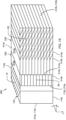
- the optical blocks 100, 200, 300 are bonded together as illustrated in FIGS. 7A - 7C to form the optical block 400 (which is a compound optical block composed of multiple sub-blocks), while maintaining the alignment described with reference to FIGS. 6A - 6C .
- the optical block 400 is a rectangular cuboid and has three regions, namely one region having the optical block (stack) 200 which carries the bonded LOEs 20 with facets 28, another region having the optical block 300 which carries the facets 38, and another region having the optical block 100 which carries the facets 18.
- the three regions are non-overlapping, and the three optical blocks 100, 200, 300 have the same thickness.
- the faces 112 a , 212 b form a first pair of parallel faces 412 a , 412 b of the optical block 400
- the face 414 a (formed from coplanar faces 114 a , 214 a , 314 a ) and the face 414 b (formed from coplanar faces 114 b , 214 b , 314 b ) form a second pair of parallel faces of the optical block 400
- the face 416 a formed from coplanar faces 116 a , 216 a , 316 a
- the face 416 b formed from coplanar faces 116 b , 216 b , 316 b
- neither one of the three pairs of faces 412 a , 412 b , 414 a , 414 b , 416 a , 416 b necessarily needs to be a pair of parallel faces.
- the major surface 24a of the LOE 20 at the top end of the stack 200 forms part of the top face 414 a of the optical block 400
- the major surface 24 b of the LOE 20 at the bottom end of the stack 200 forms part of the bottom face 414 b of the optical block 400.
- the optical blocks 100, 200, 300 can be bonded together in stages.
- the optical blocks 200, 300 can be bonded together, and then the optical blocks 100, 300 can be bonded together.
- the optical blocks 100, 300 can be bonded together, and then the optical blocks 200, 300 can be bonded together.
- the optical blocks 200, 300 are bonded together such that the face 312 b is joined to the face 212 a .
- the optical blocks 100, 300 are bonded together such that the face 112 b is joined to the face 312 a .
- the facets 18 are non-parallel to the facets 28.
- the optical blocks 100, 200, 300 are arranged such that the optical block 300 is positioned between the optical block 100, 200, resulting in the facets 38 being located between the facets 18, 28.
- the order of the optical blocks is different from that shown in the drawings, for example in which the optical block 100 is positioned between the optical block 200, 300, resulting in the facets 18 being located between the facets 28, 38.
- the face 312 a of the optical block 300 forms the face 412 a of the optical block 400.
- the optical block 300 can be omitted or replaced with one or more optical blocks carrying facets at different orientations from the facets 38. Therefore, the optical block 400 can generally be considered as being formed from two optical sub-blocks and having two regions, where the optical block 200 with facets 28 forms a first of the sub-blocks (a first region), and the optical block 100 with facets 18 forms a second of the sub-blocks (a second region).
- the second sub-block includes two sub-sub-blocks (two sub-regions), where the facets 18 are located in the first sub-sub-block (first sub-region), which in this case is optical block 100, and the facets 38 are located in the second sub-sub-block (second sub-region), which in this case is optical block 300.
- the optical blocks 100, 200 are bonded together to form the optical block 400 such that the face 112 b is joined to the face 212 a .
- the facets 18 are non-parallel to the facets 28.
- FIGS. 8A - 9B illustrate steps for cutting the optical block 400 ( FIGS. 8A and 8B ) and the result of cutting the optical block 400 ( FIGS. 9A and 9B ).
- the optical block 400 is cut along a cutting plane 402 that passes through the face 412a (which in the illustrated embodiment is face 112 a , but may be face 312 a in embodiments in which the positions of the optical blocks 100, 300 are exchanged) and at least one of the faces 116 a , 216 a , 316 a .
- the cutting plane 402 passes through the face 416 a .
- the location of the cutting plane 402 is such that the cutting plane 402 at least passes through a portion of the optical sub-block having the facets 18 or facets 38.
- the cutting plane 402 passes through a portion of the optical sub-block having the facets 18, which in the illustrated embodiment is the optical block 100.
- the cutting plane 402 may pass through all three regions of the optical block 400 (i.e., pass through regions which in combination contain facets 18, 38, 28).
- the cutting plane 402 is oblique to the face 412 a ( 112 a or 312 a), and may also be oblique to one or more of the faces 116 a , 316 a , 412 b , 112 b , 312 a , 312 b , 212 a , depending on the construction of the optical block 400.
- the cutting plane 402 is preferably perpendicular to the face 114 a (and therefore also perpendicular to faces 314 a, 214 a in embodiments in which the faces 114 a , 314 a , 214 a are parallel).
- the cutting of the optical block 400 along cutting plane 402 results in the formation of an optical structure 400' having an interfacing surface 404 (or "face" 404) at the location of the cutting plane 402, as illustrated in FIGS. 9A and 9B .
- the location of the cutting plane 402 can be restricted such that the cutting plane 402 only passes through a portion of the optical block 100 and does not pass through any of the other optical blocks 200, 300 such that the portion to be cut is exclusively part of the optical block 100.
- the location of the cutting plane 402 may be such that the cutting plane 402 passes through a portion of the optical block 300 and may also pass through a portion of the optical block 200.
- the portion of the optical block 400 that is cut-off (i.e., removed) is a triangular prism (typically a right triangular prism) portion (represented in FIGS. 8A and 8B by 401).
- the portion 401 includes a portion (typically the entirety) of the face 116 a and a portion (which may be a minority portion, for example roughly 10% - 20%) of the face 112 a .
- the location of the cutting plane can be restricted such that the cutting plane 402 only passes through a portion of the optical block 300 and does not pass through any of the other optical blocks 100, 200, such that the portion to be cut is exclusively part of the optical block 300.
- the cutting plane 402 may pass through a portion of the optical block 100 and may also pass through a portion of the optical block 200.
- FIGS. 9A and 9B illustrate the optical structure 400', having the interfacing surface 404, that is formed as result of cutting the optical block 400 along the cutting plane 402 and removing triangular prims portion 401.
- the optical block 500 having coupling-in reflectors, is bonded to the optical structure 400' at the interfacing surface 404.
- the optical block 500 is formed from a light-transmitting material and has a set of reflective internal surfaces 42 (highly reflective minors), each of which is used as a coupling-in configuration for the final compound LOE.
- the optical block 500 includes three pairs of faces (major external surfaces), namely a pair of preferably parallel faces 512 a , 512 b , a pair of faces 514 a , 514 b (which may or may not be parallel faces), and a pair of faces 516 a , 516 b (which may or may not be parallel faces).
- the three pairs of faces of the optical block 500 are mutually orthogonal (perpendicular), however, other embodiments may be preferred in which the pairs of faces are not mutually orthogonal.
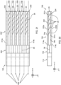
- the optical block 500 can be formed from a plurality of bonded, transparent coated plates 502 (each plate being formed from a light-transmitting material and coated with a partially reflective coating) to form reflective internal surfaces 42 that are inclined obliquely to either or both of the faces 512 a , 512 b at a predetermined angle.
- FIG. 10D illustrates one such method, in which the coated plates 502 are stacked and bonded (similar to as in FIGS. 3C , 4C , and 5C ), and then cut along equally spaced parallel cutting planes 504 (which in the arbitrarily labeled xyz coordinate system are parallel to the yz plane) to produce sliced-out optical structures 505.
- One of the optical structures 505 is used to form the optical block 500.
- the coatings used to form coated plates 502 are not partially reflective but rather are fully (and preferably highly) reflective, such that the resultant internal surfaces 42 act as fully reflective mirrors.
- Dielectric coatings are one example of suitable coatings that can be used to form the reflective internal surfaces 42.
- the cutting planes 504 are obliquely angled relative to the coated faces the plates 502, where the oblique angle of the planes 504 determines the oblique angle at which the internal surfaces 42 are inclined relative to faces 512 a , 512 b .
- each of the optical structures 505 can be cut along two additional parallel planes 506, 508 that are perpendicular to planes 504 in order to form surfaces 514 a , 514 b such that the optical block 500 has a rectangular cross-section.
- the planes 506, 508 are parallel to the xy plane.
- FIGS. 11A and 11B show the optical block 500 and the optical structure 400' prior to being bonded together to form optical structure 600 ( FIGS. 12A and 12B ).
- the optical block 500 and the optical structure 400' Prior to bonding, it is important that the optical block 500 and the optical structure 400' are appropriately aligned such that the orientation of the internal surfaces 42 is non-parallel to the orientations of the facets 18, 28, 38 (i.e., such that the internal surfaces 42 are non-parallel to the facets 18, 28, 38), and such that each internal surface 42 is associated with a respective one of the LOEs 20 in the optical block 200 such that the projection of the internal surface in the thickness dimension of the respective LOE (which in the arbitrarily labeled xyz coordinate system in the drawings is the yz plane) is bounded by the major surfaces 24 a , 24 b of the LOE 20.
- each of the faces 514 a , 414 a is in a plane parallel to the xy plane, and that each of the faces 514 b , 414 b is in a plane parallel to the xy plane.
- the optical block 500 preferably has the same thickness (measured along the z-axis, i.e., between faces 514 a , 514 b ) as the constituent optical blocks 100, 200, 300, and thus the same thickness as the optical structure 400'.
- the alignment of the optical block 500 with the optical structure 400' is preferably such that the faces 514 a , 414 a are coplanar, as are the faces 514 b , 414 b .
- the alignment of the optical block 500 with the optical structure 400' is also such that the faces 512 b , 404 are aligned and practically coincident.
- optical block 500 and the optical structure 400' are bonded together as illustrated in FIGS. 12A and 12B to form optical structure 600 (which is an intermediate work product of a compound LOE fabrication process).
- the bonding of the optical block 500 and the optical structure 400' is such that the face 512 b is joined to the face (interfacing surface) 404, while maintained the alignment described above.
- the faces 512 b , 404 are equally dimensioned, or very close to equally dimensioned.
- alignment of the optical block 500 with the optical structure 400' can also include twisting or rotating the face 512 b relative to the interfacing surface 404, such that the internal surfaces 42 are tilted at angle relative to the optical structure 400' in addition to being inclined relative to either or both of the faces 512 a , 512 b .
- such a tilt angle and inclination angle correspond to the internal surfaces 42 being inclined at two angles relative to the xy plane.
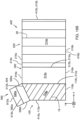
- the optical structure 600 is cut (sliced) along two or more preferably parallel cutting planes 602 at predetermined intervals in order to extract one or more compound LOEs.
- the cutting planes 602 are preferably parallel to the major external surfaces 24 a , 24 b of the LOEs 20 that form the optical block 200.
- consecutive cutting planes 602 are located between the surfaces 24 a , 24 b of consecutive LOEs 20, in particular the bonding regions formed between the surfaces 24 a , 24 b of consecutive LOEs 20.
- a first 602-1 of the cutting planes 602 passes between the bonding region between the second surface 24b-1 of a first one 20-1 of the LOEs 20 and the first surface 24a-2 of a second one 20-2 of the LOEs 20 that is adjacent to the first LOE 20-1 and bonded to the first LOE 20-1
- a second 602-2 of the cutting planes 602 that is adjacent to the first cutting plane 602-1 passes between the bonding region between second surface 24 b-2 of the second LOE 20-2 and the first surface 24a-3 of a third one 20-3 of the LOEs 20 that is adjacent to the second LOE 20-2 and bonded to the second LOE 20-2.
- the bonding regions (formed between the surfaces 24 a , 24 b of consecutive LOEs 20) can provide guides for placement of the cutting planes 602. It is further noted that minor deviations from parallelism of the cutting planes which result in the two major surfaces, formed by cutting along consecutive cutting planes 602, of a sliced-out compound LOE being approximately parallel but not perfectly parallel can be corrected by polishing the compound LOEs along the two major surfaces.
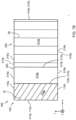
- the compound LOE 700 includes a first pair of faces 712 a , 712 b (that include parts of faces 412 a , 412 b , and which may or may not be parallel faces), a second pair of parallel faces 714 a , 714 b (major surfaces) formed by cutting the optical structure 600 along consecutive cutting planes 602 (and preferably formed in part by surfaces 24 a , 24 b of one of the LOEs 20), and a third pair of faces 716 a , 716 b (that include parts of faces 416 a , 416 b , and which may or may not be parallel faces).
- the compound LOE 700 has a first plurality of facets 18 (in a first LOE region 710) having a first orientation and which also may be inclined obliquely to the faces 714 a , 714 b or orthogonal to the faces 714 a , 714 b , a second plurality of facets 28 (in a second LOE region 720) inclined obliquely to the faces 714 a , 714 b and having an orientation non-parallel to the orientation of the facets 18, and at least one facet 38 located in a region 730 between the first and second LOE regions and having an orientation parallel to the faces 714 a , 714 b and non-parallel to the orientations of the facets 18, 28.
- the compound LOE 700 also includes a (highly) reflective internal surface 42 (also referred to as a coupling-in reflector) located in a coupling-in region 750 bounded by faces 512 a , 514 a ', 514 b ' 516 a , 516 b , and having an orientation that is non-parallel to the orientations of the facets 18, 28, 38 (i.e., reflective internal surface 42 is non-parallel to the facets 18, 28, 38).
- Faces 514 a ', 514 b ' are mutually parallel faces and form part of faces 714 a , 714 b .
- the reflective surface 42 is tilted about two axes relative to the waveguide axes (which can be a tilt angle measured relative to the x-axis and the y-axis in the arbitrarily labeled xyz coordinate system in the drawings).
- the compound LOE 700 does not have a rectangular cross-section in the two-dimensional planes (mostly noticeable in the xy plane shown in FIG. 14B ), due to the cutting and bonding steps described above with reference to FIGS. 8A - 12B .
- each of the compound LOEs can be polished on the external surfaces 714 a , 714 b in order to form a final compound LOE having a desired thickness (measured along the z-axis in the arbitrarily labeled xyz coordinate system in the drawings), and to ensure parallelism between the surfaces 714 a , 714 b (and the optional facet 38).
- FIG. 15 shows one view of the resulting polished compound LOE, with parallel surfaces 714 a ', 714 b ' corresponding to the surfaces 714 a , 714 b after being polished.
- the compound LOE produced using the fabrication process according to the embodiments disclosed herein provide several advantages over compound LOEs produced using conventional fabrication methods.
- the location of the cutting plane 402 at the specified region of the optical block 400 ( FIGS. 8A and 8B ) accommodates placement of the coupling-in reflector 42 in a region that presents a more aesthetic overall design of the compound LOE 700.
- the spatial positioning of the coupling-in reflector 42 which is determined by the oblique angle of the cutting plane 402 and the oblique angle of the cutting planes 504 ( FIG. 10D ), determines the spatial orientation of the image projector that produces collimated image light.
- the spatial orientation of the coupling-in reflector 42 can be designed to accommodate spatial positioning of the image projector below the compound LOE in association with a portion of the face 714 b ' at or near the coupling-in region 750, thereby providing aesthetic placement of the image projector and reducing the overall formfactor of the optical system formed from the compound LOE and image projector, which can be implemented as part of a head-mounted display and in certain non-limiting implementations as part of an eyeglasses formfactor.
- the compound LOE according to the disclosed embodiments can be attached or otherwise coupled to an image projector that produces collimated image light that can be coupled into the compound LOE by the reflective internal surface 42.
- the coupling-in reflector is designed to accommodate spatial positioning of the image projector below the compound LOE.
- the collimated image rays corresponding to the central field of view chief ray should generate an approximately perpendicular angle (up to approximately 20°) with relation to the compound LOE both at the input to the compound LOE from the image projector (i.e., input to the first LOE region via coupling-in from the reflective internal surface 42) and at the output of compound LOE to the eye of the observer (i.e., output from the second LOE region via facets 28).
- the reflective internal surface 42 and the facets 28 have similar elevation angle.
- the oblique angle of the reflective internal surface 42 measured relative to the faces 512 a , 512 b is often approximately equal to the oblique angle of the facets 28 measured relative to the faces 714 a ', 714 b ' (or equivalently measured relative to surfaces 24 a , 24 b of the constituent LOE 20 that forms the compound LOE).
- the reflective internal surface 42 provides a useful active area that couples light from the image projector into the compound LOE, while the remaining portions of the reflective internal surface 42 either do not couple any light into the compound LOE, or couple in light at angles which result in unwanted reflections at major surfaces of the compound LOE that give rise to ghost images.
- the reflective coatings used to form coated plates 502 ( FIG. 10D ) for producing reflective internal surface 42 typically have a high cost, and therefore reduction of any unused (i.e., "inactive" ) area of the internal surfaces 42 can reduce manufacturing costs.
- the size of the reflective internal surfaces 42 may be limited to the active area, and to fill the remaining area with a less expensive inert material (such as glass, plastic, or even metal).
- a reduced-sized reflective internal surface 42 is produced from a reduced-sized optical block 500' that is bonded together with one or more blocks 800, 900 of inert material such as, for example, glass, plastic, or metal.
- the material used to form blocks 800, 900 can be the same or different.
- both blocks 800, 900 can be formed from glass, or one of the blocks can be formed from glass and the other formed from plastic.
- the optical block 500' is similar in structure to the optical block 500, with the noted exception being that the length of the optical block 500' (which in the arbitrarily labeled xyz coordinate system in the drawings is measured along the y-axis) is reduced compared to the length of the optical block 500, thereby limiting the size of the internal surfaces 42 to only the useful active area. Due to the similarity of the structure of the optical blocks 500', 500, like reference numerals will be used to identify like components, with an apostrophe (" ' ”) appended to the reference numerals of the optical block 500'.
- the inert block 800 has three pairs of faces (major external surfaces), namely a first pair of preferably parallel faces 812 a , 812 b , a second pair of faces 814 a , 814 b (which may or may not be parallel faces), and a third pair of faces 816 a , 816 b (which may or may not be parallel faces).
- the optical block 500' is limited in size by the inert block 800, and therefore the inert block 800 can be understood to function as a ghost-reducing element, which limits the size of the internal surfaces 42 to only the useful active area.
- the block 800 is a rectangular cuboid.
- the inert block 900 also has three pairs of parallel faces (major external surfaces), namely a first pair of preferably parallel faces 912 a , 912 b , a second pair of faces 914 a , 914 b (which may or may not be parallel faces), and a third pair of faces 916 a , 916 b (which may or may not be parallel faces).
- the block 900 is a rectangular cuboid.
- the block 900 is optional, but can be used to advantage to provide structural reinforcement and support to the optical block 500'.
- the bonding is preferably performed in stages, where the optical block 500' and the block 800 are first bonded together to form compound block 580.
- the blocks 500', 800 are appropriately aligned prior to being bonded together.
- the alignment of the blocks 500', 800 can be understood as follows: the faces 512 a ', 812 a are in a plane parallel to the yz plane and are preferably coplanar, the faces 512 b ', 812 b are in a plane parallel to the yz plane and are preferably coplanar, the faces 514 a ', 814 a are in a plane parallel to the xy plane and are preferably coplanar, the faces 514 b ', 814 b are in a plane parallel to the xy plane and are preferably coplanar, and the faces 516 b ', 816 a are aligned
- the blocks 500', 800 are bonded together to form compound block 580 such that the face 516 b ' is joined to the face 816 a , while maintaining the alignment described with reference to FIGS. 16A and 16B .
- Block 580 is shown in FIGS.
- 17A and 17B has a first pair of preferably parallel faces 582 a , 582 b respectively formed from faces 512 a ', 812 a and 512 b ', 812 b , a second pair of faces 584 a , 584 b (which may or may not be parallel faces) respectively formed from faces 514 a ', 814 a and 514 b ', 814 b , and a third pair of faces 516 a ', 816 b (which may or may not be parallel faces).
- the internal surfaces 42 are in a first region of the block 580 and are inclined obliquely to the faces 582 a , 582 b .
- the blocks 580, 900 can then be bonded together to form compound block 590, as illustrated in FIGS. 18A and 18B .
- the blocks 580, 900 are appropriately aligned prior to being bonding together. With reference to the coordinate system shown in FIGS.
- the alignment of the blocks 580, 900 (when each of the blocks 580, 900 is constructed as a rectangular cuboid) can be understood as follows: the faces 516 a ', 916 a are in a plane parallel to the xz plane and are preferably coplanar, the faces 516 b ', 916 b are in a plane parallel to the xz plane and are preferably coplanar, the faces 584 a , 914 a are in a plane parallel to the xy plane and are preferably coplanar, the faces 584 b , 914 b are in a plane parallel to the xy plane and are preferably coplanar, and the faces 582 a , 912 b are aligned in a plane parallel to the yz plane and are coincident.
- Block 590 is shown in FIGS. 18A and 18B and has a first pair of parallel faces 912 a , 582 b , a second pair of faces 594 a , 594 b (which may or may not be parallel faces) respectively formed from faces 914 a , 584 a and 914 b , 584 b , and a third pair of faces 596 a , 596 b (which may or may not be parallel faces) respectively formed from faces 916 a , 586 a and 916 b , 586 b .
- Block 590 can then be aligned and bonded together with the optical structure 400' in place of optical block 500, similar to as described with reference to FIGS. 11A - 12B .
- the bonding of block 590 together with the optical structure 400' is such that the face 582 b is joined to interfacing surface 404, as shown in FIGS. 19A and 19B .
- the face 512 b ' which forms part of face 582 b .
- the optical structure formed as a result of bonding together block 590 and optical structure 400' can then be sliced at predetermined intervals demarcated by parallel cutting planes in order to extract one or more compound LOEs, similar to as described with reference to FIG. 13 .
- the inert block 900 can be bonded without the inert block 800 in order to provide structural reinforcement and support to the optical block 500.
- the inert block 900 and the optical block 500 are bonded together to form an intermediate block such that the face 912 b is joined to the face 512 a of the optical block 500.
- the inert block 900 and the optical block 500 are appropriately aligned prior to being bonding together.
- the inert block 900 and the optical block 500' are bonded together without the presence block 800.
- the bonding is such that that the face 912 b is joined to the face 512 a ' of the optical block 500'.
- the inert block 900 and the optical block 500' are appropriately aligned prior to being bonding together.
- the size of the inert block 900 can be reduced to match the size of the optical block 500'.
- a transparent cover plate on either or both of the polished surfaces 714 a ', 714 b ' of the sliced-out compound LOE, such as the compound LOE illustrated in FIG. 15 .
- such transparent cover plates can be provided directly to the surfaces 714 a ', 714 b ' (i.e., after the sliced-out compound LOE is polished).
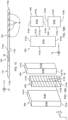
- the transparent cover plates can be provided as spacer plates between the LOEs 20 during production of the optical block 200, as shown in FIGS. 20A and 20B .
- FIG. 20A there is illustrated an aligned arrangement 220 of LOEs 20 and transparent cover plates 220, in which the LOEs 20 and the cover plates 230 alternate along a length of the arrangement 220 perpendicular to the parallel faces 24 a , 24 b of the LOEs 20 (here the length is along the z-axis).
- Each cover plate 230 has a pair of parallel external faces 231 a , 231 b .
- the cover plates 230 and the LOEs 20 are bonded together to form a bonded stack 200' (also referred to as optical block 200'), as shown in FIG. 20B .
- the bonding is such that the faces 231 b , 24 a of adjacent cover plates 230 and LOEs 20 are joined, and such that the faces 231 a , 24 b of adjacent cover plates 230 and LOEs 20 are joined.
- the stack 200' is generally similar in structure to the stack 200 of FIG. 3A (i.e., the stack 200' has three pairs of parallel faces and is formed from a plurality of bonded LOEs) and the like reference numerals will be used to denote like elements.
- the stack 200' is a bonded stack of LOEs 20 and cover plates 230 in which the LOEs 20 and the cover plates 230 alternate along a length of the stack 200' that is perpendicular to the faces 214 a , 214 b (and parallel to faces 212 a , 212 b ).
- These transparent cover plates 230 are also referred to as transparent spacer plates, as they provide spacing between consecutive LOEs.
- the thickness of the coated plates 302 used in forming optical block 300 should be adjusted to account for the overall thickness of the optical block 200' and to ensure that alignment of the optical blocks 200', 300 results in each facet 38 being located in a plane that is halfway between the major surfaces 24 a , 24 b of the associated LOE 20 such that the optical blocks 200', 300 are bonded together at the proper alignment.
- the consecutive cutting planes should pass through consecutive spacer plates 230 having one of the LOEs 20 therebetween, as illustrated in FIG. 21 , and preferably pass approximately through the center of the spacer plates 230.
- FIG. 22 An example of a sliced-out compound LOE 700 having two transparent cover plates 232, 234 is illustrated in FIG. 22 .
- the cover plates 232, 234 are formed from two of the cover plates 230 in the stack 200' that are sliced along two of the cutting planes 602.
- the cover plates 232, 234 are bonded to the LOE 20 such that the face 231 b of cover plate 232 is joined to the face 24 a of LOE 20, and the face 231 a of cover plate 234 is joined to the face 24 b of LOE 20.
- the face 233 a of the cover plate 232 (which is opposite face from face 231 b of cover plate 232), and the face 233 b of the cover plate 234 (which is opposite from face 231 a of cover plate 234) respectively form part of the major external surfaces 714 a , 714 b of the compound LOE 700.
- the surfaces 714 a , 714 b of the compound LOE of FIG. 22 can then polished, similar to as described above with reference to FIG. 15 to achieve a final compound LOE having a desired thickness and to ensure parallelism between the faces 714 a , 714 b .
- the embodiments described herein have pertained to bonding the optical block 500 (or 500') to the optical structure 400' such that the coupling-in reflector 42 accommodates spatial positioning of the image projector below the final compound LOE product
- other embodiments are possible which accommodate different spatial positioning of the image projector.
- the optical block 500 can be inverted (for example by exchanging the positions of the faces 514 a , 514 b ) such that the internal surfaces 42 are inclined upward, rather than downward as shown in FIGS. 10A, 10B , 11A , and 12A .
- Such a configuration allows deployment of the image projector above the final compound LOE product.
- additional optical components such as prisms
- the optical block 500 can be optically coupled or bonded with the optical block 500 (or 500'), with or without inert blocks 800 and/or 900, prior to slicing-out the compound LOE in order to provide additional coupling-in geometries of the final compound LOE product.
- one or more additional optical components such as a prism, can be optically coupled or bonded with the coupling-in reflector 42 at the coupling-in region 750.
- the present disclosure has described various cutting steps in which optical materials are cut along cutting planes in order to produce various optical blocks and sub-components of optical blocks. It is noted that in certain embodiments, some or all of the surfaces that result from these cutting steps can be polished prior to bonding steps.
- the joined faces of the optical blocks 100, 200, 300 can be polished prior to bonding together the optical blocks 100, 200, 300.
- the major surfaces of the LOEs used to form the optical block 200 can be polished prior to forming the bonded stack of LOEs (optical block 200).
- the interfacing surface 404 and the joining face of the optical block 500 can be polished prior to bonding together the optical blocks 400, 500.
- suitable optical alignment apparatus / device(s) / tool(s) can include, for example, one or more computerized control device, one or more computerized processing device, one or more optical subsystem having, for example, one or more light source, one or more light detector/sensor, one or more optics (e.g., one or more lens, folding optics, etc.), autocollimators, and the like.
- the cutting or slicing of the optical blocks and the optical structures described herein can be performed by any suitable cutting apparatus / device / tool, as should be understood by those of ordinary skill in the art.
- the polishing of the faces and surfaces of the optical blocks and optical structures (including the compound LOEs) described herein can be performed by any suitable polishing apparatus / device / tool, as should be understood by those of ordinary skill in the art.
Landscapes
- Physics & Mathematics (AREA)
- General Physics & Mathematics (AREA)
- Optics & Photonics (AREA)
- Engineering & Computer Science (AREA)
- Microelectronics & Electronic Packaging (AREA)
- Optical Elements Other Than Lenses (AREA)
- Non-Portable Lighting Devices Or Systems Thereof (AREA)
Abstract
Description
- This application claims priority from
US Provisional Patent Application No. 63/235,837, filed August 23, 2021 - The present invention relates to light-guide optical elements (LOEs), and in particular, methods for manufacturing compound LOEs for two-dimensional aperture expansion having embedded coupling-in reflectors.
- Compound LOEs or "two-dimensional expansion waveguides" have been described in various publications by Lumus Ltd (Israel). In general terms, these compound LOEs employ two regions, each of which is a parallel-faced block of transparent material (i.e., light-transmitting material) for facilitating the propagation of light corresponding to a collimated image by internal reflection at major surfaces, and includes a set of mutually-parallel, internal, partially-reflective surfaces (or "facets"), which redirect the collimated image light while achieving expansion of the optical aperture. By combining two such elements with different facet orientations, it is possible to achieve two-dimensional expansion of the optical aperture within a single compound element, thereby expanding an input image from an image projector and outputting the expanded image over a large area towards the eye of an observer.
- Embodiments of the present invention provide methods of fabrication of compound LOEs.
- According to the teachings of an embodiment of the present invention, there is provided a method of fabricating a compound light-guide optical element (LOE). The method comprises: obtaining a stack having a first pair of faces and a plurality of LOEs, each of the LOEs having a pair of major parallel surfaces and a first plurality of mutually parallel partially reflective internal surfaces oblique to the pair of major parallel surfaces; obtaining a first optical block having a second pair of faces and a second plurality of mutually parallel partially reflective internal surfaces; bonding together the first optical block and the stack such that one of the faces of the first pair of faces is joined to one of the faces of the second pair of faces and such that the first plurality of partially reflective internal surfaces is non-parallel to the second plurality of partially reflective internal surfaces, thereby forming a second optical block; cutting the second optical block along a cutting plane that passes through the other one of the faces of the second pair of faces, thereby forming a first optical structure having an interfacing surface at the cutting plane; obtaining a third optical block having a third pair of faces and a plurality of mutually parallel reflective internal surfaces; bonding together the third optical block and the first optical structure such that one of the faces of the third pair of faces is joined to the interfacing surface and such that the plurality of reflective internal surfaces is non-parallel to both the first plurality of partially reflective internal surfaces and the second plurality of partially reflective internal surfaces, thereby forming a second optical structure; and slicing out at least one compound LOE from the second optical structure by cutting the second optical structure through at least two cutting planes substantially parallel to the major parallel surfaces of consecutive LOEs.
- Optionally, the method further comprises: for each sliced-out compound LOE, polishing external surfaces of the sliced-out compound LOE formed by cutting the optical structure along two consecutive of the cutting planes.
- Optionally, the first optical block has a pair of parallel faces, and the second plurality of partially reflective internal surfaces are perpendicular to the pair of parallel faces of the first optical block.
- Optionally, the first optical block has a pair of parallel faces, and the second plurality of partially reflective internal surfaces are oblique to the pair of parallel faces of the first optical block.
- Optionally, the first optical block has a third plurality of mutually parallel partially reflective internal surfaces non-parallel to the first and second pluralities of partially reflective internal surfaces.
- Optionally, the first optical block has a first region that includes the second plurality of partially reflective internal surfaces and a second region that includes the third plurality of partially reflective internal surfaces, the first and second regions of the first optical block are non-overlapping regions.
- Optionally, the third plurality of partially reflective internal surfaces are parallel to the major parallel surfaces of the LOEs.
- Optionally, each respective one of the third partially reflective internal surfaces is located in a plane that is approximately halfway between the pair of major parallel surfaces of a respective one of the LOEs.
- Optionally, the third plurality of partially reflective internal surfaces is located between the first and second pluralities of partially reflective internal surfaces.
- Optionally, the second plurality of partially reflective internal surfaces is located between the first and third pluralities of partially reflective internal surfaces.
- Optionally, the first optical block is formed by bonding together first and second constituent optical blocks that each have a pair of faces such that one of the faces of the pair of faces of the first constituent optical block is joined to one of the faces of the pair of faces of the second constituent optical block, the first constituent optical block includes the second plurality of partially reflective internal surfaces, and the second constituent optical block includes a third plurality of mutually parallel partially reflective internal surfaces non-parallel to the first plurality of partially reflective internal surfaces and non-parallel to the second plurality of partially reflective internal surfaces.
- Optionally, the third optical block and the first optical structure are bonded together such that substantially the entirety of the one of the faces of the third pair of faces is joined to substantially the entirety of the interfacing surface.
- Optionally, the third optical block and the first optical structure are bonded together such that the one of the faces of the third pair of faces is joined to a fractional portion of the interfacing surface.
- Optionally, the third optical block has an additional pair of faces, the method and the further comprises: obtaining an inert block having first and second pairs of faces; and bonding together the inert block and the third optical block such that one of the faces of the first pair of faces of the inert block is joined to one of the faces of the additional pair of faces of the third optical block, thereby forming a compound block having first and second faces, the first face of the compound block formed from the one of the faces of the third pair of faces and one of the faces of the second pair of faces of the inert block, and the second face of the compound block formed from the other one of the faces of the third pair of faces and the one of the faces of the second pair of faces of the inert block.
- Optionally, the method further comprises: obtaining a second inert block having a pair of faces; and bonding together the second inert block and the compound block such that one of the faces of the pair of faces of the second inert block is joined to the second face of the compound block.
- Optionally, bonding together the third optical block and the first optical structure includes: bonding together the compound block and the first optical structure such that the first face of the compound block is joined to the interfacing surface.
- Optionally, the method further comprises: obtaining an inert block having a pair of faces; and bonding together the inert block and the third optical block such that one of the faces of the pair of faces of the second inert block is joined to the other one of the faces of the third pair of faces of the optical block.
- Optionally, the stack is a bonded stack of the LOEs and a plurality of transparent spacer plates, the LOEs and the transparent spacer plates alternate along a length of the stack perpendicular to the major parallel surfaces of the LOEs.
- Optionally, the at least two cutting planes are located in consecutive spacer plates having one of the LOEs therebetween.
- There is also provided according to an embodiment of the teachings of the present invention a method of fabricating a compound light-guide optical element (LOE). The method comprises: obtaining a first optical block that comprises: at least a first pair of faces, a first region formed from a stack of LOEs, each of the LOEs having a pair of major parallel surfaces and a set plurality of mutually parallel partially reflective internal surfaces located between the parallel surfaces and inclined obliquely to the parallel surfaces such that the first region comprises a first plurality of partially reflective internal surfaces, and a second region having a second plurality of mutually parallel partially reflective internal surfaces non-parallel to the first plurality of partially reflective internal surfaces; cutting the first optical block along a cutting plane that passes through one of the faces of the first pair of faces, thereby forming a first optical structure having an interfacing surface at the cutting plane; obtaining a second optical block having a second pair of faces and a plurality of mutually parallel reflective internal surfaces; bonding together the first optical structure and the second optical block such that one of the faces of the second pair of faces is joined to the interfacing surface and such that the plurality of reflective internal surfaces is non-parallel to both the first plurality of partially reflective internal surfaces and the second plurality of partially reflective internal surfaces, thereby forming a second optical structure; and slicing out at least one compound LOE from the second optical structure by cutting the second optical structure through at least two cutting planes substantially parallel to the major parallel surfaces of consecutive LOEs.
- Optionally, the stack is a bonded stack of the LOEs and a plurality of transparent spacer plates, the LOEs and the transparent spacer plates alternate along a length of the stack perpendicular to the major parallel surfaces of the LOEs.
- Optionally, the at least two cutting planes are located in consecutive spacer plates having one of the LOEs therebetween.
- Optionally, the first optical block further includes an additional pair of faces, one of major parallel surfaces of the LOE at a top end of the stack forms part of one of the faces of the additional pair of faces, and one of major parallel surfaces of the LOE at a bottom end of the stack forms part of the other one of the faces of the additional pair of faces.
- Optionally, the second optical sub-block includes a first sub-block region and a second sub-block region, the second plurality of partially reflective internal surfaces are located in the first sub-block region, a third plurality of mutually parallel partially reflective internal surfaces are located in the second sub-block region, and the third plurality of partially reflective internal surfaces are non-parallel to the first plurality of partially reflective internal surfaces and non-parallel to the second plurality of partially reflective internal surfaces.
- Optionally, the third plurality of partially reflective internal surfaces is located between the first and second pluralities of partially reflective internal surfaces.
- Optionally, the second plurality of partially reflective internal surfaces is located between the first and third pluralities of partially reflective internal surfaces.
- There is also provided according to an embodiment of the teachings of the present invention a method of fabricating a compound light-guide optical element (LOE). The method comprises: obtaining a first optical block having a first pair of faces and a first plurality of mutually parallel partially reflective internal surfaces; obtaining a second optical block formed as a stack of LOEs and having a second pair of faces, each of the LOEs having a pair of major parallel surfaces and a second plurality of mutually parallel partially reflective internal surfaces oblique to the pair of major parallel surfaces; obtaining a third optical block having a third pair of faces and a third plurality of mutually parallel partially reflective internal surfaces; bonding together the first and third optical blocks and bonding together the second and third optical blocks to form a fourth optical block, the bonding is such that: i) one of the faces of the first pair of faces is joined to one of the faces of the third pair of faces, ii) one of the faces of the second pair of faces is joined to the other one of the faces of the third pair of faces, iii) the third plurality of partially reflective internal surfaces is substantially parallel to the major parallel surfaces of the LOEs, and iv) the first, second, and third pluralities of partially reflective internal surfaces are mutually non-parallel; cutting the fourth optical block along a cutting plane that passes through the other one of the faces of the first pair of faces, thereby forming a first optical structure having an interfacing surface at the cutting plane; obtaining a fifth optical block having a fourth pair of faces and a plurality of mutually parallel reflective internal surfaces; bonding together the first optical structure and the fifth optical block to form a second optical structure, the bonding together the first optical structure and the fifth optical block is such that one of the faces of the fourth pair of faces is joined to the interfacing surface and such that the plurality of reflective internal surfaces is non-parallel to the first, second, and third pluralities of partially reflective internal surfaces; and slicing out at least one compound LOE from the second optical structure by cutting the second optical structure through at least two cutting planes substantially parallel to the major parallel surfaces of consecutive LOEs.
- Optionally, the stack is a bonded stack of the LOEs and a plurality of transparent spacer plates, the LOEs and the transparent spacer plates alternate along a length of the stack perpendicular to the major parallel surfaces of the LOEs.
- Optionally, the at least two cutting planes are located in consecutive spacer plates having one of the LOEs therebetween.
- There is also provided according to an embodiment of the teachings of the present invention a method of fabricating a compound light-guide optical element (LOE). The method comprises: obtaining a first optical block having a first pair of faces and a first plurality of mutually parallel partially reflective internal surfaces; obtaining a second optical block formed as a stack of LOEs and having a second pair of faces, each of the LOEs having a pair of major parallel surfaces and a second plurality of mutually parallel partially reflective internal surfaces oblique to the pair of major parallel surfaces; obtaining a third optical block having a third pair of faces and a third plurality of mutually parallel partially reflective internal surfaces; bonding together the first and third optical blocks and bonding together the first and second optical blocks to form a fourth optical block, the bonding is such that: i) one of the faces of the third pair of faces is joined to one of the faces of the first pair of faces, ii) one of the faces of the second pair of faces is joined to the other one of the faces of the first pair of faces, iii) the third plurality of partially reflective internal surfaces is substantially parallel to the major parallel surfaces of the LOEs, and iv) the first, second, and third pluralities of partially reflective internal surfaces are mutually non-parallel; cutting the fourth optical block along a cutting plane that passes through the other one of the faces of the third pair of faces, thereby forming a first optical structure having an interfacing surface at the cutting plane; obtaining a fifth optical block having a fourth pair of faces and a plurality of mutually parallel reflective internal surfaces; bonding together the first optical structure and the fifth optical block to form a second optical structure, the bonding together the first optical structure and the fifth optical block is such that one of the faces of the fourth pair of faces is joined to the interfacing surface and such that the plurality of reflective internal surfaces is non-parallel to the first, second, and third pluralities of partially reflective internal surfaces, thereby forming a second optical structure; and slicing out at least one compound LOE from the second optical structure by cutting the second optical structure through at least two cutting planes substantially parallel to the major parallel surfaces of consecutive LOEs.
- Optionally, the stack is a bonded stack of the LOEs and a plurality of transparent spacer plates, the LOEs and the transparent spacer plates alternate along a length of the stack perpendicular to the major parallel surfaces of the LOEs.
- Optionally, the at least two cutting planes are located in consecutive spacer plates having one of the LOEs therebetween.
- Unless otherwise defined herein, all technical and/or scientific terms used herein have the same meaning as commonly understood by one of ordinary skill in the art to which the invention pertains. Although methods and materials similar or equivalent to those described herein may be used in the practice or testing of embodiments of the invention, exemplary methods and/or materials are described below. In case of conflict, the patent specification, including definitions, will control. In addition, the materials, methods, and examples are illustrative only and are not intended to be necessarily limiting.
- Some embodiments of the present invention are herein described, by way of example only, with reference to the accompanying drawings. With specific reference to the drawings in detail, it is stressed that the particulars shown are by way of example and for purposes of illustrative discussion of embodiments of the invention. In this regard, the description taken with the drawings makes apparent to those skilled in the art how embodiments of the invention may be practiced.
- Attention is now directed to the drawings, where like reference numerals or characters indicate corresponding or like components. In the drawings:
-
FIGS. 1A - 1C are schematic side, front, and plan views, respectively, of a compound LOE having a first LOE region with a first set of partially reflective internal surfaces and a second LOE region with a second set of partially reflective internal surfaces non-parallel to the first set of partially reflective internal surfaces; -
FIGS. 2A and 2B are schematic side and front views, respectively, of a compound LOE similar to the compound LOE ofFIGS. 1A - 1C , but including a third region with one or more third partially reflective internal surfaces; -
FIG. 3A is a schematic side view of an optical block formed as a bonded stack of LOEs that can be used to form second LOE regions of compound LOEs, according to embodiments of the present invention; -
FIG. 3B is a schematic side view of one of the LOEs of the stack ofFIG. 3A ; -
FIG. 3C is a schematic side view of a bonded stack of coated plates that can be cut at predetermined intervals to produce the LOEs ofFIG. 3A ; -
FIG. 3D is a schematic side view of LOEs arranged in a formation prior to bonding to form the stack ofFIG. 3A ; -
FIGS. 4A and 4B are schematic front and isometric views, respectively, of an optical block having a plurality of partially reflective surfaces that can be used to form first LOE regions of compound LOEs, according to embodiments of the present invention; -
FIG. 4C is a schematic front view of a bonded stack of coated plates that can be cut at predetermined intervals to produce the optical block ofFIGS. 4A and 4B ; -
FIGS. 5A and 5B are schematic front and isometric views, respectively, of an optical block having a plurality of partially reflective surfaces that can be used to form third LOE regions of compound LOEs, according to embodiments of the present invention; -
FIG. 5C is a schematic side view of a bonded stack of coated plates that can be cut at predetermined intervals to produce the optical block ofFIGS. 5A and 5B ; -
FIGS. 6A - 6C are schematic isometric, front, and side views, respectively, of the optical blocks ofFIGS. 3A ,4A ,4B ,5A, and 5B in alignment prior to being bonded together, according to embodiments of the present invention; -
FIGS. 7A - 7C are schematic isometric, front, and side views, respectively, corresponding toFIGS. 6A - 6C , showing the optical blocks bonded together to form a new optical block, according to embodiments of the present invention; -
FIGS. 8A and8B are schematic isometric and front views, respectively, of a cutting plane along which the optical block ofFIGS. 7A - 7C is cut to produce a new optical structure, according to embodiments of the present invention; -
FIGS. 9A and9B are schematic isometric and front views, respectively, of the optical structure formed by cutting the optical structure ofFIGS. 8A and8B along the cutting plane; -
FIGS. 10A - 10C are schematic isometric, side, and front views, respectively, of an optical block having a plurality of reflective internal surfaces that can be used to form coupling-in reflectors of compound LOEs, according to embodiments of the present invention; -
FIG. 10D is a schematic side view of a bonded stack of coated plates that can be cut at predetermined intervals to produce the optical block ofFIGS. 10A - 10C ; -
FIGS. 11A and11B are schematic isometric and front views, respectively of the optical structure ofFIGS. 9A and9B and the optical block ofFIGS. 10A - 10C in alignment prior to being bonded together, according to embodiments of the present invention; -
FIGS. 12A and12B are schematic isometric and front views, respectively, corresponding toFIGS. 11A and11B , showing the optical structure and the optical block bonded together to form a new optical structure, according to embodiments of the present invention; -
FIG. 13 is a schematic side view of the optical structure ofFIGS. 12A and12B showing cutting planes at predetermined intervals along which the optical structure can be cut to extract one or more compound LOEs, according to embodiments of the present invention; -
FIGS. 14A - 14C are schematic side, front, and plan views, respectively, of a compound LOE sliced-out from the optical structure ofFIGS. 12A and12B after cutting the optical structure along two consecutive cutting planes ofFIG. 13 , according to embodiments of the present invention; -
FIG. 15 is a schematic side view of a final compound LOE produced from the compound LOE ofFIGS. 14A - 14C by polishing two of the major external surfaces of compound LOE ofFIGS. 14A - 14C , according to embodiments of the present invention; -
FIGS. 16A and 16B are schematic isometric and front views, respectively, of a reduced-sized optical block similar to the optical block ofFIGS. 10A - 10C , in alignment with first and second inert blocks prior to being bonded together with the first inert block, according to embodiments of the present invention; -
FIGS. 17A and 17B are schematic isometric and front views, respectively, corresponding toFIGS. 16A and 16B , showing the first inert block and the optical block bonded together to form a compound block and in alignment with the second inert block prior to the compound block and the second inert block being bonded together, according to embodiments of the present invention; -
FIGS. 18A and 18B are schematic isometric and front views, respectively, corresponding toFIGS. 17A and 17B , showing the second inert block and the compound block bonded together to form a second compound block, according to embodiments of the present invention; -
FIGS. 19A and19B are schematic isometric and front views, respectively, similar toFIGS. 12A and12B , but showing the compound block ofFIGS. 18A and 18B and the optical structure ofFIGS. 9A and9B bonded together to form an optical structure, according to embodiments of the present invention -
FIG. 20A is a schematic side view similar toFIG. 3D , but showing the LOEs arranged in alternating formation with a plurality of transparent cover plates prior to the LOEs and the transparent cover plates being bonded together, according to embodiments of the present invention; -
FIG. 20B is a schematic side view of the alternating LOEs and transparent cover plates ofFIG. 20A bonded together to form an optical block that can be used to form a first LOE region of a compound LOE, according to embodiments of the present invention; -
FIG. 21 is a schematic side view of an optical structure similar to the optical structure ofFIG. 13 , but in which the optical structure includes the optical block ofFIG. 20B , according to embodiments of the present invention; and -
FIG. 22 is a schematic side view of a compound LOE sliced-out from the optical structure ofFIG. 21 after cutting the optical structure along two consecutive cutting planes, according to embodiments of the present invention. - Embodiments of the present invention provide methods of fabrication of compound LOEs.
- The principles and operation of the methods according to present invention may be better understood with reference to the drawings accompanying the description. The accompanying drawings are provided with an xyz coordinate system that is arbitrarily labeled but which is consistent between the drawings. This xyz coordinate system is used herein to better explain the disclosed embodiments by providing a common reference frame among the drawings.
- Before explaining at least one embodiment of the invention in detail, it is to be understood that the invention is not necessarily limited in its application to the details of construction and the arrangement of the components and/or methods set forth in the following description and/or illustrated in the drawings and/or the examples. The invention is capable of other embodiments or of being practiced or carried out in various ways.
- Referring now to the drawings,
FIGS. 1A - 1C illustrate various views of acompound LOE 1. Thecompound LOE 1 includes afirst LOE 10 and asecond LOE 20 that are bonded together at aninterface 40. Typically, the twoLOEs - The
first LOE 10 is formed from a light-transmitting material and includes a first pair offaces LOE 10 between thefaces LOE 10 is configured to guide light (image illumination), corresponding to a collimated image injected into theLOE 10 by an image projector (not shown), such that the light (represented inFIG. 1B by light ray 50) is trapped in one dimension by internal reflection (preferably but not exclusively total internal reflection) at theparallel faces LOE 10. TheLOE 10 is further configured to gradually couple the propagating (trapped) light out of theLOE 10 via thefacets 18, which are inclined obliquely to the direction of propagation of the light and each reflect a proportion of the intensity of the propagating light, thereby expanding the image illumination in one dimension (which in this case is approximately along the y-axis). In the drawings, the light coupled out of theLOE 10 by thefacets 18 is represented by light rays 60 (FIGS. 1A and 1B ), and the propagation of the collimatedimage light 50 by internal reflection at the faces of theLOE 10 is represented by left-going and right-going rays 52 (FIG. 1A ). - In general, the
facets 18 have a first orientation in thecompound LOE 1. In certain embodiments, thefacets 18 are obliquely angled relative tofaces facets 18 are orthogonal to thefaces facets 18 can be obliquely angled to one or both of thefaces facets 18 can be orthogonal to one or both of thefaces FIGS. 1A and 1B , thefaces facets 18 are inclined obliquely to thefaces - The reflectivity of the
facets 18 can be provided via coatings on the internal surfaces prior to forming theLOE 10. The reflectance of each of thefacets 18 may be the same, or the reflectivity of thefacets 18 may be different from one another and may increase along a light propagation direction (which in the arbitrarily labeled xyz coordinate system in the drawings is along the y-axis). - The light that is coupled out of the
LOE 10 is coupled into thesecond LOE 20. TheLOE 20 is also formed from a light-transmitting material and includes a first pair offaces faces faces compound LOE 1. Likewise, thefaces compound LOE 1. Thefaces compound LOE 1, and thefaces compound LOE 1. The remaining two external surfaces of thecompound LOE 1 are respectively formed from thefaces - The
facets 28 have a second orientation in thecompound LOE 1 that is non-parallel to the first orientation of thefacets 18. The reflectivity of thefacets 28 can be provided via coatings on the internal surfaces prior to forming theLOE 20. The reflectance of each of thefacets 28 may be the same, or the reflectivity of thefacets 28 may be different from one another and may increase along a light propagation direction (which in the arbitrarily labeled xyz coordinate system in the drawings is along the x-axis). - The light from
LOE 10 is coupled into theLOE 20 through interface 40 (which is coincident with theface 12b and theface 22a). TheLOE 20 is configured to guide the light by internal reflection (preferably but not exclusively total internal reflection) at thefaces LOE 20 via thefacets 28, which each reflect a proportion of the intensity of the propagating light, toward the eye of an observer, thereby expanding the image illumination in a second dimension (which in this case is along the x-axis). InFIG. 1A , the propagation of image light through theLOE 20 by internal reflection atfaces rays rays rays LOE 20 from theLOE 10. The light coupled out of theLOE 20 by thefacets 28 is represented inFIG. 1A bylight rays 64. - The image illumination that is to be coupled into the
compound LOE 1 for guiding by theLOE 10 and theLOE 20 is generated by an external image projector (not shown), which is typically implemented as a micro-projector arrangement formed from a microdisplay device (such as an LCoS chip) that generates image illumination, and collimating optics for collimating the image illumination to produce collimated image illumination. The collimated image illumination is coupled into theLOE 10 by a coupling-in optical arrangement, in the form of a highly reflectiveinternal surface 42 in a coupling-in region of theLOE 10. - In order to fill the
LOE 20 with the collimated image illumination (whereby both the image and its conjugate propagate through the LOE by internal reflection) while maintaining a small input aperture (small projector), it is preferable to employ at least one additional partially reflective internal surface having a particular orientation relative to thefacets FIGS. 2A and 2B illustrate a compound LOE having such anadditional facet 38. Thefacet 38 can be deployed in part of theLOE 10, or as shown inFIGS. 2A and 2B as part of a separate light-transmittingsubstrate 30 having three pairs offaces faces facet 38 is parallel to thefaces facets single facet 38, thefacet 38 is preferably located halfway betweenfaces faces facet 38, thefacets 38 are preferably evenly spaced betweenfaces FIGS. 2A and 2B , theLOE 10 and thesubstrate 30 are bonded together atfaces substrate 30 and theLOE 20 are bonded together atfaces facet 38 is located between the sets offacets facets 18 are located between thefacet 38 and the set offacets 28, depending on the design specification of the specific application for the compound LOE. - In the illustrated embodiment, the light 60 (coupled-out by facets 18) is partially reflected by the
facet 38. The reflected and transmitted parts of light 60 are coupled into theLOE 20, and correspond torays - Further details of compound LOEs, including compound LOEs that may be similar to the compound LOEs illustrated in
FIGS. 1A - 2B , can be found in various publications by Lumus Ltd. (Israel), including, for example,US Patent Application Publication No. 2021/0247608 ,PCT publication WO 2021/240513 ,PCT publication WO 2021/152602 ,PCT publication WO 2021/001841 , andUS Patent No. 10,551,544 - Embodiments of the present invention are directed to methods of fabricating compound LOEs. The compound LOEs that are fabricated according to the methods of the present invention may be different in structure from the compound LOEs illustrated in
FIGS. 1A - 2B , but have similar components, as will become apparent from the ensuing description. The fabrication method steps are described in detail below with reference toFIGS. 3A - 21 , and generally include steps of obtaining an optical block 400 (FIGS. 7A - 7C ) having sets of therequisite facets 18, 28 (and preferably also a set of facets 38) embedded in regions of theoptical block 400 and appropriately oriented relative to each other such that thefacets 18, 28 (and 38) are mutually non-parallel, cutting a portion of theoptical block 400 at a prescribed cutting plane (FIGS. 8A and8B ) that is at a prescribed angle and passes through particular faces of theoptical block 400 to form an optical structure 400' having an interfacing surface (FIGS. 9A and9B ) formed at the cutting plane, obtaining an additional optical block 500 (FIGS. 10A - 10D ) having a set of reflectiveinternal surfaces 42 embedded therein, and bonding theoptical block 500 to the optical structure 400' at the interface surface to form an intermediate optical structure 600 (FIGS. 12A and12B ) having embedded therein sets of therequisite facets 18, 28 (and preferably also a set of facets 38) and a set of the reflectiveinternal surfaces 42 that is non-parallel to thefacets optical structure 600 is then cut along two or more cutting planes in order to slice-out one or more compound LOEs (FIGS. 13 - 14B ), where each compound LOE hasfacets 18 and facets 28 (and preferably also at least one facet 38) and an embedded reflectiveinternal surface 42. Each of the sliced-out compound LOEs can then be polished to achieve a final compound LOE having a desired thickness (FIG. 15 ). In certain embodiments, one ormore blocks optical block 500 to form a compound block 590 (FIGS. 16A - 18B ), which is then bonded to the optical structure 400' (FIGS. 19A and19B ) to form the intermediateoptical structure 600. As will be discussed, obtaining theoptical block 400 can include producing theoptical block 400 by obtaining various otheroptical blocks FIGS. 3A - 5C ) and bonding thoseoptical blocks optical block 400. Each of theoptical blocks facets - It is noted that in the drawings, and in accordance with one set of non-limiting embodiments of the present invention, each of the
various blocks - The following paragraphs describe the structure and production of the
optical block 200 with reference toFIGS. 3A - 3D . Referring first toFIG. 3A , there is shown theoptical block 200, which is formed as a stack ofLOEs 20 that are bonded together. Theoptical block 200 has at least two pairs of faces (major external surfaces), namely a pair of preferablyparallel faces faces faces optical block 200 also includes a third pair of faces that may or may not be a pair of parallel faces, and may also be perpendicular to one or more of thefaces FIG. 3A , but are shown in various other drawings, includingFIGS. 6B ,7B ,8B ,9B ,11B ,12B , and19B . As will become apparent, thefaces - Each of the
LOEs 20 in the stack ofFIG. 3A is an LOE as illustrated inFIG. 3B . ThisLOE 20 is also generally similar to thesecond LOE 20 discussed above with reference to FIGS. 1A - 2C. As shown inFIG. 3B , and as discussed above with reference to FIGS. 1A - 2C, eachLOE 20 is formed from a light-transmitting material havingparallel faces internal facets 28 inclined obliquely to thefaces US Patent No. 7,634,214 ,US Patent No. 8,873,150 ,PCT publication WO 2016/103263 , andPCT publication WO 2020/212835 . -
FIG. 3C shows one example method of fabricating a plurality ofLOEs 20, which can be used to produce theoptical block 200. InFIG. 3C , a plurality of light-transmitting plates is coated to formcoated plates 202 which are stacked and bonded together, and then cut along equally spaced parallel cutting planes 206 (which in the arbitrarily labeled xyz coordinate system are parallel to the xy plane). Each of theplates 202 has a pair of parallel faces (surfaces) 204a, 204b which are appropriately coated with coatings that provide the reflectivity of the facets 28 (such that thefacets 28 are partially reflective). The cutting planes 206 are oblique to thefaces facets 28, and the resulting cuts along the cuttingplanes 206 define thefaces LOEs 20. The cutting planes 206 are spaced at predetermined intervals. Preferably the predetermined intervals are uniform intervals such that the cuttingplanes 206 are uniformly spaced. The uniform spacing is preferably in the range of 1 - 2 millimeters, such that the thickness of each LOE 20 (measured betweenfaces - Prior to bonding together the
LOEs 20 to form theoptical block 200, theLOEs 20 are first aligned and arranged in a formation 210 (FIG. 3D ). TheLOEs 20 in theformation 210 are then bonded together to form the optical block 200 (FIG. 3A ) as a bonded stack ofLOEs 20, such that thefaces LOEs 20 are joined together at bonding regions, and such that the sets ofinternal facets 28 of theLOEs 20 constitute a plurality offacets 28 of theoptical block 200. As can be seen fromFIGS. 3A and3D , themajor surface 24a of theLOE 20 at the top end of thestack 200 forms thetop face 214a of thestack 200, and themajor surface 24b of theLOE 20 at the bottom end of thestack 200 forms thebottom face 214b of thestack 200. - The following paragraphs describe the structure and production of the
optical block 100 with reference toFIGS. 4A - 4C . Referring first toFIGS. 4A and 4B , theoptical block 100 is formed from a light-transmitting material and has an embedded set of thefacets 18. Theoptical block 100 includes three pairs of faces (major external surfaces), namely a pair offaces parallel faces faces optical block 100 are mutually orthogonal (perpendicular), which can simplify the fabrication process. - The
optical block 100 can be formed from a plurality of bonded, transparent coated plates 102 (each plate being formed from a light-transmitting material and coated with a partially reflective coating) to formfacets 18 that are angled relative to thefaces 114a, 114 at a predetermined angle, i.e., thefacets 18 may be inclined obliquely relative to thefaces faces facets 18 may also be inclined obliquely to thefaces optical block 100.FIG. 4C illustrates one such method, in which thecoated plates 102 are stacked and bonded together (similar to as inFIG. 3C ), and then cut along a first pair of preferablyparallel cutting planes 104 and along a second pair of preferablyparallel cutting planes 106 that are preferably perpendicular to theplanes 104, in order to extract theoptical block 100. In embodiments in which thefacets 18 are oblique to one or both of thefaces planes 104 relative to the faces of thecoated plates 102 determines the angle at which thefacets 18 are inclined relative tofaces planes 104 define thefaces optical block 100, and the cuts along cuttingplanes 106 define thefaces optical block 100. - In certain embodiments, such as the embodiment illustrated in
FIG. 4C , the cuttingplanes plates 102 such that theresultant facets 18 are perpendicular to thefaces optical block 100. In the arbitrarily labeled xyz coordinate system used in the drawings, when the cuttingplanes plates 102, the cuttingplanes 104 are parallel to the yz plane and the cuttingplanes 106 are parallel to the xz plane. The cutting planes 106 are perpendicular to theplanes 104. - As noted above, other embodiments are possible in which the
facets 18 are inclined obliquely to thefaces faces - The following paragraphs describe the structure and production of the
optical block 300 with reference toFIGS. 5A - 5C . Referring first toFIGS. 5A and 5B , theoptical block 300 is formed from a light-transmitting material and has an embedded set of thefacets 38. Theoptical block 300 includes three pairs of faces (major external surfaces), namely a pair offaces parallel faces faces optical block 100 are mutually orthogonal (perpendicular). - The
optical block 300 can be formed from a plurality of bonded, transparent coated plates 302 (each plate being a formed from a light-transmitting material and coated with a partially reflective coating) to formfacets 38 that are parallel tofaces faces optical block 300.FIG. 5C illustrates one such method, in which thecoated plates 302 are stacked and bonded (similar to as inFIGS. 3C and4C ), and then cut along a pair of cuttingplanes 304 in order to extract theoptical block 100. In certain embodiments, such as the embodiment illustrated inFIG. 5C , theplanes 304 are parallel planes (which in the arbitrarily labeled xyz coordinate system are parallel to the yz plane). However, as alluded to above, parallelism between theplanes 304 is not a strict requirement, and in certain cases it may be advantageous to cut along non-parallel cutting planes, which can improve compactness and overall form factor of the final compound LOE product. In certain embodiments, theplanes 304 are perpendicular to the major external surfaces (faces) of theplates 202. However, this perpendicularity is also not an optical requirement for producing the final compound LOE product, but is rather a matter of practical convenience when fabricating the compound LOE. The stacked and bonded plates may also be cut along an additional pair of cuttingplanes 306 that pass through two of the plates, and may be parallel to the major external surfaces of theplates 202 and perpendicular toplanes 304. In the arbitrarily labeled xyz coordinate system used in the drawings, the cuttingplanes 306 are parallel to the xy plane. - With continued reference to
FIGS. 1A - 5C , refer now toFIGS. 6A - 6C which show the threeoptical blocks FIGS. 7A - 7C ). Prior to bonding, it is important that theoptical blocks facets 18 is non-parallel to the orientation of thefacets 28, and such that the orientation of thefacets 38 is non-parallel to the orientations of thefacets blocks facets - It also preferable that the
optical block 300 is aligned with theoptical block 200 such that thefacets 38 ofoptical block 300 are in planes that are parallel to the planes offaces optical block 200. In embodiments in which each compound LOE is to have only asingle facet 38, theoptical blocks respective facet 38 is located in a plane that is approximately halfway between the majorexternal surfaces LOEs 20 that forms theoptical block 200. In embodiments in which each compound LOE is to have multiple facets 38 (say N facets 38), theoptical blocks N facets 38, theN facets 38 are evenly spaced between the majorexternal surfaces LOEs 20 that forms theoptical block 200. It is noted, however, that theblock 300 can be positioned relative to theblock 200 without applying too much scrutiny with respect to the positioning of thefacets 38 relative to the majorexternal surfaces facets 38 relative to the majorexternal surfaces - With reference to the coordinate system shown in
FIGS. 6A - 6C , the alignment of theoptical blocks faces faces faces faces faces faces optical blocks facets 38 is in a plane that is parallel to the xy plane. - In order to reduce wastage, the
optical blocks faces faces faces - Employing
optical blocks optical blocks faces faces faces faces faces faces - Once properly aligned, the
optical blocks FIGS. 7A - 7C to form the optical block 400 (which is a compound optical block composed of multiple sub-blocks), while maintaining the alignment described with reference toFIGS. 6A - 6C . In the illustrated embodiment, theoptical block 400 is a rectangular cuboid and has three regions, namely one region having the optical block (stack) 200 which carries the bondedLOEs 20 withfacets 28, another region having theoptical block 300 which carries thefacets 38, and another region having theoptical block 100 which carries thefacets 18. In the illustrated embodiment, the three regions are non-overlapping, and the threeoptical blocks faces parallel faces optical block 400, theface 414a (formed fromcoplanar faces face 414b (formed fromcoplanar faces optical block 400, and theface 416a (formed fromcoplanar faces face 416b (formed fromcoplanar faces optical block 400. It is noted that in embodiments in which theblock 400 is not a rectangular cuboid, neither one of the three pairs offaces - As can be seen from
FIGS. 3A ,3D ,7A and 7D, themajor surface 24a of theLOE 20 at the top end of thestack 200 forms part of thetop face 414a of theoptical block 400, and themajor surface 24b of theLOE 20 at the bottom end of thestack 200 forms part of thebottom face 414b of theoptical block 400. - In certain embodiments, the
optical blocks optical blocks optical blocks optical blocks optical blocks optical blocks face 312b is joined to theface 212a. Theoptical blocks face 112b is joined to theface 312a. As a result of the bonding (and proper aligning) of theoptical blocks facets 18 are non-parallel to thefacets 28. - In certain embodiments, such as the embodiments illustrated in the drawings, the
optical blocks optical block 300 is positioned between theoptical block facets 38 being located between thefacets optical block 100 is positioned between theoptical block facets 18 being located between thefacets face 312a of theoptical block 300 forms theface 412a of theoptical block 400. - The embodiments described thus far have pertained to employing three optical blocks to form compound
optical block 400. However, in certain embodiments theoptical block 300 can be omitted or replaced with one or more optical blocks carrying facets at different orientations from thefacets 38. Therefore, theoptical block 400 can generally be considered as being formed from two optical sub-blocks and having two regions, where theoptical block 200 withfacets 28 forms a first of the sub-blocks (a first region), and theoptical block 100 withfacets 18 forms a second of the sub-blocks (a second region). In the embodiments illustrated in the drawings, the second sub-block includes two sub-sub-blocks (two sub-regions), where thefacets 18 are located in the first sub-sub-block (first sub-region), which in this case isoptical block 100, and thefacets 38 are located in the second sub-sub-block (second sub-region), which in this case isoptical block 300. - In embodiments in which
optical block 300 is omitted, theoptical blocks optical block 400 such that theface 112b is joined to theface 212a. As a result of the bonding (and proper aligning) of theoptical blocks facets 18 are non-parallel to thefacets 28. - With continued reference to
FIGS. 1A - 7B , refer now toFIGS. 8A - 9B , which illustrate steps for cutting the optical block 400 (FIGS. 8A and8B ) and the result of cutting the optical block 400 (FIGS. 9A and9B ). Generally speaking, and as shown inFIGS. 8A and8B , theoptical block 400 is cut along a cuttingplane 402 that passes through theface 412a (which in the illustrated embodiment isface 112a, but may beface 312a in embodiments in which the positions of theoptical blocks faces faces face 416a, the cuttingplane 402 passes through theface 416a. The location of the cuttingplane 402 is such that the cuttingplane 402 at least passes through a portion of the optical sub-block having thefacets 18 orfacets 38. In the illustrated embodiment, the cuttingplane 402 passes through a portion of the optical sub-block having thefacets 18, which in the illustrated embodiment is theoptical block 100. However, in some practical implementations, the cuttingplane 402 may pass through all three regions of the optical block 400 (i.e., pass through regions which in combination containfacets - In certain embodiments, the cutting
plane 402 is oblique to theface 412a (112a or 312a), and may also be oblique to one or more of thefaces optical block 400. The cuttingplane 402 is preferably perpendicular to theface 114a (and therefore also perpendicular tofaces faces optical block 400 along cuttingplane 402 results in the formation of an optical structure 400' having an interfacing surface 404 (or "face" 404) at the location of the cuttingplane 402, as illustrated inFIGS. 9A and9B . - In some of the embodiments in which the
optical block 400 comprises the threeoptical blocks FIGS. 7A - 7C , the location of the cuttingplane 402 can be restricted such that the cuttingplane 402 only passes through a portion of theoptical block 100 and does not pass through any of the otheroptical blocks optical block 100. However, in other embodiments, the location of the cuttingplane 402 may be such that the cuttingplane 402 passes through a portion of theoptical block 300 and may also pass through a portion of theoptical block 200. - In embodiments in which the
faces face 416a, the portion of theoptical block 400 that is cut-off (i.e., removed) is a triangular prism (typically a right triangular prism) portion (represented inFIGS. 8A and8B by 401). In embodiments in which theoptical block 300 is sandwiched between theoptical blocks portion 401 includes a portion (typically the entirety) of theface 116a and a portion (which may be a minority portion, for example roughly 10% - 20%) of theface 112a. - In some of the embodiments in which the positions of the
optical blocks optical block 100 is sandwiched between theoptical blocks plane 402 only passes through a portion of theoptical block 300 and does not pass through any of the otheroptical blocks optical block 300. However, similar to as mentioned above, in certain embodiments the cuttingplane 402 may pass through a portion of theoptical block 100 and may also pass through a portion of theoptical block 200. -
FIGS. 9A and9B illustrate the optical structure 400', having the interfacingsurface 404, that is formed as result of cutting theoptical block 400 along the cuttingplane 402 and removingtriangular prims portion 401. Theoptical block 500, having coupling-in reflectors, is bonded to the optical structure 400' at theinterfacing surface 404. - The following paragraphs describe the structure and production of the
optical block 500 with reference toFIGS. 10A - 10D . Referring first toFIGS. 10A - 10C , theoptical block 500 is formed from a light-transmitting material and has a set of reflective internal surfaces 42 (highly reflective minors), each of which is used as a coupling-in configuration for the final compound LOE. Theoptical block 500 includes three pairs of faces (major external surfaces), namely a pair of preferablyparallel faces faces faces optical block 500 are mutually orthogonal (perpendicular), however, other embodiments may be preferred in which the pairs of faces are not mutually orthogonal. - The
optical block 500 can be formed from a plurality of bonded, transparent coated plates 502 (each plate being formed from a light-transmitting material and coated with a partially reflective coating) to form reflectiveinternal surfaces 42 that are inclined obliquely to either or both of thefaces optical block 500.FIG. 10D illustrates one such method, in which thecoated plates 502 are stacked and bonded (similar to as inFIGS. 3C ,4C , and5C ), and then cut along equally spaced parallel cutting planes 504 (which in the arbitrarily labeled xyz coordinate system are parallel to the yz plane) to produce sliced-outoptical structures 505. One of theoptical structures 505 is used to form theoptical block 500. Unlike the coatings used to produce thefacets coated plates 502 are not partially reflective but rather are fully (and preferably highly) reflective, such that the resultantinternal surfaces 42 act as fully reflective mirrors. Dielectric coatings are one example of suitable coatings that can be used to form the reflective internal surfaces 42. The cutting planes 504 are obliquely angled relative to the coated faces theplates 502, where the oblique angle of theplanes 504 determines the oblique angle at which theinternal surfaces 42 are inclined relative tofaces - In certain embodiments, each of the
optical structures 505 can be cut along two additionalparallel planes planes 504 in order to formsurfaces optical block 500 has a rectangular cross-section. In the arbitrarily labeled xyz coordinate system, theplanes - With continued reference to
FIGS. 8A - 10D , attention is also directed toFIGS. 11A and11B which show theoptical block 500 and the optical structure 400' prior to being bonded together to form optical structure 600 (FIGS. 12A and12B ). Prior to bonding, it is important that theoptical block 500 and the optical structure 400' are appropriately aligned such that the orientation of theinternal surfaces 42 is non-parallel to the orientations of thefacets internal surfaces 42 are non-parallel to thefacets internal surface 42 is associated with a respective one of theLOEs 20 in theoptical block 200 such that the projection of the internal surface in the thickness dimension of the respective LOE (which in the arbitrarily labeled xyz coordinate system in the drawings is the yz plane) is bounded by themajor surfaces LOE 20. - In certain embodiments, it may also be preferable that each of the
faces faces - In order to avoid wastage at the final cutting step for slicing-out the compound LOE, the
optical block 500 preferably has the same thickness (measured along the z-axis, i.e., betweenfaces optical blocks optical block 500 with the optical structure 400' is preferably such that thefaces faces optical block 500 with the optical structure 400' is also such that thefaces - Once properly aligned, the
optical block 500 and the optical structure 400' are bonded together as illustrated inFIGS. 12A and12B to form optical structure 600 (which is an intermediate work product of a compound LOE fabrication process). The bonding of theoptical block 500 and the optical structure 400' is such that theface 512b is joined to the face (interfacing surface) 404, while maintained the alignment described above. Preferably, thefaces optical block 500 with the optical structure 400' can also include twisting or rotating theface 512b relative to theinterfacing surface 404, such that theinternal surfaces 42 are tilted at angle relative to the optical structure 400' in addition to being inclined relative to either or both of thefaces internal surfaces 42 being inclined at two angles relative to the xy plane. - As illustrated in
FIG. 13 , after forming theoptical structure 600, theoptical structure 600 is cut (sliced) along two or more preferably parallel cuttingplanes 602 at predetermined intervals in order to extract one or more compound LOEs. The cutting planes 602 are preferably parallel to the majorexternal surfaces LOEs 20 that form theoptical block 200. Most preferably,consecutive cutting planes 602 are located between thesurfaces consecutive LOEs 20, in particular the bonding regions formed between thesurfaces consecutive LOEs 20. For example, a first 602-1 of the cuttingplanes 602 passes between the bonding region between thesecond surface 24b-1 of a first one 20-1 of theLOEs 20 and thefirst surface 24a-2 of a second one 20-2 of theLOEs 20 that is adjacent to the first LOE 20-1 and bonded to the first LOE 20-1, and a second 602-2 of the cuttingplanes 602 that is adjacent to the first cutting plane 602-1 passes between the bonding region betweensecond surface 24b-2 of the second LOE 20-2 and thefirst surface 24a-3 of a third one 20-3 of theLOEs 20 that is adjacent to the second LOE 20-2 and bonded to the second LOE 20-2. It is noted herein that the bonding regions (formed between thesurfaces consecutive cutting planes 602, of a sliced-out compound LOE being approximately parallel but not perfectly parallel can be corrected by polishing the compound LOEs along the two major surfaces. - With additional reference to
FIGS. 14A - 14C , there is shown onecompound LOE 700 that is sliced-out from theoptical structure 600 after cutting along cuttingplanes 602. Thecompound LOE 700 includes a first pair offaces faces parallel faces optical structure 600 along consecutive cutting planes 602 (and preferably formed in part bysurfaces faces faces compound LOE 700 has a first plurality of facets 18 (in a first LOE region 710) having a first orientation and which also may be inclined obliquely to thefaces faces faces facets 18, and at least onefacet 38 located in aregion 730 between the first and second LOE regions and having an orientation parallel to thefaces facets compound LOE 700 also includes a (highly) reflective internal surface 42 (also referred to as a coupling-in reflector) located in a coupling-inregion 750 bounded byfaces facets internal surface 42 is non-parallel to thefacets Faces 514a', 514b' are mutually parallel faces and form part offaces face 512b of the optical block 500 (orface 512b' of block 500' or face 582 ofblock 580/590) is twisted or rotated relative to theinterfacing surface 404, thereflective surface 42 is tilted about two axes relative to the waveguide axes (which can be a tilt angle measured relative to the x-axis and the y-axis in the arbitrarily labeled xyz coordinate system in the drawings). - As should be apparent, unlike the compound LOEs illustrated in
FIGS. 1A - 2B , thecompound LOE 700 does not have a rectangular cross-section in the two-dimensional planes (mostly noticeable in the xy plane shown inFIG. 14B ), due to the cutting and bonding steps described above with reference toFIGS. 8A - 12B . - After slicing-out the
compound LOEs 700, each of the compound LOEs can be polished on theexternal surfaces surfaces FIG. 15 shows one view of the resulting polished compound LOE, withparallel surfaces 714a', 714b' corresponding to thesurfaces - The compound LOE produced using the fabrication process according to the embodiments disclosed herein provide several advantages over compound LOEs produced using conventional fabrication methods. First, the location of the cutting
plane 402 at the specified region of the optical block 400 (FIGS. 8A and8B ) accommodates placement of the coupling-inreflector 42 in a region that presents a more aesthetic overall design of thecompound LOE 700. In addition, the spatial positioning of the coupling-inreflector 42, which is determined by the oblique angle of the cuttingplane 402 and the oblique angle of the cutting planes 504 (FIG. 10D ), determines the spatial orientation of the image projector that produces collimated image light. In the disclosed embodiments, the spatial orientation of the coupling-inreflector 42 can be designed to accommodate spatial positioning of the image projector below the compound LOE in association with a portion of theface 714b' at or near the coupling-inregion 750, thereby providing aesthetic placement of the image projector and reducing the overall formfactor of the optical system formed from the compound LOE and image projector, which can be implemented as part of a head-mounted display and in certain non-limiting implementations as part of an eyeglasses formfactor. Furthermore, the reduced wastage of raw materials and the fact that a large number of compound LOEs can be sliced-out from a singleoptical structure 600 as enabled by the disclosed fabrication processes, facilitates large-scale production of the compound LOEs while maintaining lower manufacturing cost compared to conventional fabrication methods used to produce compound LOEs. - As mentioned, the compound LOE according to the disclosed embodiments can be attached or otherwise coupled to an image projector that produces collimated image light that can be coupled into the compound LOE by the reflective
internal surface 42. In preferred embodiments, the coupling-in reflector is designed to accommodate spatial positioning of the image projector below the compound LOE. For both functional and aesthetic reasons, it is typically desired that the collimated image rays corresponding to the central field of view chief ray should generate an approximately perpendicular angle (up to approximately 20°) with relation to the compound LOE both at the input to the compound LOE from the image projector (i.e., input to the first LOE region via coupling-in from the reflective internal surface 42) and at the output of compound LOE to the eye of the observer (i.e., output from the second LOE region via facets 28). Accordingly, it is preferable that the reflectiveinternal surface 42 and thefacets 28 have similar elevation angle. In other words, the oblique angle of the reflectiveinternal surface 42 measured relative to thefaces facets 28 measured relative to thefaces 714a', 714b' (or equivalently measured relative tosurfaces constituent LOE 20 that forms the compound LOE). - In many cases, only a portion of the reflective
internal surface 42 provides a useful active area that couples light from the image projector into the compound LOE, while the remaining portions of the reflectiveinternal surface 42 either do not couple any light into the compound LOE, or couple in light at angles which result in unwanted reflections at major surfaces of the compound LOE that give rise to ghost images. In addition, the reflective coatings used to form coated plates 502 (FIG. 10D ) for producing reflectiveinternal surface 42 typically have a high cost, and therefore reduction of any unused (i.e., "inactive" ) area of theinternal surfaces 42 can reduce manufacturing costs. Therefore, in order to reduce manufacturing costs and mitigate ghost images by preventing or reducing unwanted reflections, it may be advantageous to limit the size of the reflectiveinternal surfaces 42 to the active area, and to fill the remaining area with a less expensive inert material (such as glass, plastic, or even metal). - With additional reference to
FIGS. 16A - 18B , the following paragraphs describe embodiments in which a reduced-sized reflectiveinternal surface 42 is produced from a reduced-sized optical block 500' that is bonded together with one ormore blocks blocks 800, 900 (referred to interchangeably herein as "inert blocks") can be the same or different. For example, bothblocks optical block 500, with the noted exception being that the length of the optical block 500' (which in the arbitrarily labeled xyz coordinate system in the drawings is measured along the y-axis) is reduced compared to the length of theoptical block 500, thereby limiting the size of theinternal surfaces 42 to only the useful active area. Due to the similarity of the structure of theoptical blocks 500', 500, like reference numerals will be used to identify like components, with an apostrophe (" ' ") appended to the reference numerals of the optical block 500'. - The
inert block 800 has three pairs of faces (major external surfaces), namely a first pair of preferablyparallel faces faces faces inert block 800, and therefore theinert block 800 can be understood to function as a ghost-reducing element, which limits the size of theinternal surfaces 42 to only the useful active area. In certain embodiments, theblock 800 is a rectangular cuboid. - The
inert block 900 also has three pairs of parallel faces (major external surfaces), namely a first pair of preferablyparallel faces faces 914a, 914b (which may or may not be parallel faces), and a third pair offaces block 900 is a rectangular cuboid. As will be discussed, theblock 900 is optional, but can be used to advantage to provide structural reinforcement and support to the optical block 500'. - The bonding is preferably performed in stages, where the optical block 500' and the
block 800 are first bonded together to formcompound block 580. Theblocks 500', 800 are appropriately aligned prior to being bonded together. With reference to the coordinate system shown inFIGS. 16A and 16B , the alignment of the blocks 500', 800 (when each of theblocks 500', 800 is constructed as a rectangular cuboid) can be understood as follows: thefaces 512a', 812a are in a plane parallel to the yz plane and are preferably coplanar, thefaces 512b', 812b are in a plane parallel to the yz plane and are preferably coplanar, thefaces 514a', 814a are in a plane parallel to the xy plane and are preferably coplanar, thefaces 514b', 814b are in a plane parallel to the xy plane and are preferably coplanar, and thefaces 516b', 816a are aligned in a plane parallel to the xz plane and are coincident. - The
blocks 500', 800 are bonded together to formcompound block 580 such that theface 516b' is joined to theface 816a, while maintaining the alignment described with reference toFIGS. 16A and 16B .Block 580 is shown inFIGS. 17A and 17B , and has a first pair of preferablyparallel faces faces 512a', 812a and 512b', 812b, a second pair offaces faces 514a', 814a and 514b', 814b, and a third pair offaces 516a', 816b (which may or may not be parallel faces). Theinternal surfaces 42 are in a first region of theblock 580 and are inclined obliquely to thefaces - In certain embodiments, the
blocks compound block 590, as illustrated inFIGS. 18A and 18B . Theblocks FIGS. 17A and 17B , the alignment of theblocks 580, 900 (when each of theblocks faces 516a', 916a are in a plane parallel to the xz plane and are preferably coplanar, thefaces 516b', 916b are in a plane parallel to the xz plane and are preferably coplanar, thefaces faces 584b, 914b are in a plane parallel to the xy plane and are preferably coplanar, and thefaces - The
blocks compound block 590 such that theface 912b is joined to theface 582a, while maintaining the alignment described with reference toFIGS. 17A and 17B .Block 590 is shown inFIGS. 18A and 18B and has a first pair ofparallel faces faces faces faces faces - Block 590 can then be aligned and bonded together with the optical structure 400' in place of
optical block 500, similar to as described with reference toFIGS. 11A - 12B . When usingblock 590 instead ofblock 500, the bonding ofblock 590 together with the optical structure 400' is such that theface 582b is joined to interfacingsurface 404, as shown inFIGS. 19A and19B . As a result, only a fractional portion of theinterfacing surface 404 is joined to theface 512b' (which forms part offace 582b). This is in contrast to the embodiment illustrated inFIGS. 12A and12B , in which the entirety of theface 512b is joined to the entirety of theinterfacing surface 404. The optical structure formed as a result of bonding together block 590 and optical structure 400' can then be sliced at predetermined intervals demarcated by parallel cutting planes in order to extract one or more compound LOEs, similar to as described with reference toFIG. 13 . - In certain embodiments, the
inert block 900 can be bonded without theinert block 800 in order to provide structural reinforcement and support to theoptical block 500. For example, in one embodiment, theinert block 900 and theoptical block 500 are bonded together to form an intermediate block such that theface 912b is joined to theface 512a of theoptical block 500. In such an embodiment, theinert block 900 and theoptical block 500 are appropriately aligned prior to being bonding together. - In another similar embodiment, the
inert block 900 and the optical block 500' are bonded together without thepresence block 800. In such an embodiment, the bonding is such that that theface 912b is joined to theface 512a' of the optical block 500'. In such an embodiment, theinert block 900 and the optical block 500' are appropriately aligned prior to being bonding together. Optionally, the size of theinert block 900 can be reduced to match the size of the optical block 500'. - In certain embodiments, it may be advantageous to provide a transparent cover plate on either or both of the
polished surfaces 714a', 714b' of the sliced-out compound LOE, such as the compound LOE illustrated inFIG. 15 . In certain embodiments, such transparent cover plates can be provided directly to thesurfaces 714a', 714b' (i.e., after the sliced-out compound LOE is polished). - In other embodiments, the transparent cover plates can be provided as spacer plates between the LOEs 20 during production of the
optical block 200, as shown inFIGS. 20A and20B . Looking first atFIG. 20A , there is illustrated an alignedarrangement 220 ofLOEs 20 andtransparent cover plates 220, in which theLOEs 20 and thecover plates 230 alternate along a length of thearrangement 220 perpendicular to theparallel faces cover plate 230 has a pair of parallelexternal faces cover plates 230 and theLOEs 20 are bonded together to form a bondedstack 200' (also referred to asoptical block 200'), as shown inFIG. 20B . The bonding is such that thefaces adjacent cover plates 230 andLOEs 20 are joined, and such that thefaces adjacent cover plates 230 andLOEs 20 are joined. - The
stack 200' is generally similar in structure to thestack 200 ofFIG. 3A (i.e., thestack 200' has three pairs of parallel faces and is formed from a plurality of bonded LOEs) and the like reference numerals will be used to denote like elements. One notable difference betweenstacks stack 200' is a bonded stack ofLOEs 20 andcover plates 230 in which theLOEs 20 and thecover plates 230 alternate along a length of thestack 200' that is perpendicular to thefaces faces transparent cover plates 230 are also referred to as transparent spacer plates, as they provide spacing between consecutive LOEs. - In embodiments in which
optical block 200' is provided, havingLOEs 20 provided withspacer plates 230 therebetween, the thickness of thecoated plates 302 used in formingoptical block 300 should be adjusted to account for the overall thickness of theoptical block 200' and to ensure that alignment of theoptical blocks facet 38 being located in a plane that is halfway between themajor surfaces LOE 20 such that theoptical blocks optical block 200' instead ofoptical block 200, the consecutive cutting planes should pass throughconsecutive spacer plates 230 having one of theLOEs 20 therebetween, as illustrated inFIG. 21 , and preferably pass approximately through the center of thespacer plates 230. - An example of a sliced-out
compound LOE 700 having twotransparent cover plates FIG. 22 . Thecover plates cover plates 230 in thestack 200' that are sliced along two of the cutting planes 602. Thecover plates LOE 20 such that theface 231b ofcover plate 232 is joined to theface 24a ofLOE 20, and theface 231a ofcover plate 234 is joined to theface 24b ofLOE 20. Theface 233a of the cover plate 232 (which is opposite face fromface 231b of cover plate 232), and theface 233b of the cover plate 234 (which is opposite fromface 231a of cover plate 234) respectively form part of the majorexternal surfaces compound LOE 700. Thesurfaces FIG. 22 can then polished, similar to as described above with reference toFIG. 15 to achieve a final compound LOE having a desired thickness and to ensure parallelism between thefaces - Although the embodiments described herein have pertained to bonding the optical block 500 (or 500') to the optical structure 400' such that the coupling-in
reflector 42 accommodates spatial positioning of the image projector below the final compound LOE product, other embodiments are possible which accommodate different spatial positioning of the image projector. For example, theoptical block 500 can be inverted (for example by exchanging the positions of thefaces internal surfaces 42 are inclined upward, rather than downward as shown inFIGS. 10A, 10B ,11A , and12A . Such a configuration allows deployment of the image projector above the final compound LOE product. - Although not illustrated in the drawings, additional optical components, such as prisms, can be optically coupled or bonded with the optical block 500 (or 500'), with or without
inert blocks 800 and/or 900, prior to slicing-out the compound LOE in order to provide additional coupling-in geometries of the final compound LOE product. Alternatively, in addition, one or more additional optical components, such as a prism, can be optically coupled or bonded with the coupling-inreflector 42 at the coupling-inregion 750. - The present disclosure has described various cutting steps in which optical materials are cut along cutting planes in order to produce various optical blocks and sub-components of optical blocks. It is noted that in certain embodiments, some or all of the surfaces that result from these cutting steps can be polished prior to bonding steps. For example, the joined faces of the
optical blocks optical blocks optical block 200 can be polished prior to forming the bonded stack of LOEs (optical block 200). Furthermore, theinterfacing surface 404 and the joining face of theoptical block 500 can be polished prior to bonding together theoptical blocks - The alignment of the various blocks and structures described herein can be performed using any suitable optical alignment apparatus / device(s) / tool(s) that perform suitable optical alignment techniques / methods. Such suitable optical alignment apparatus / device(s) / tool(s) can include, for example, one or more computerized control device, one or more computerized processing device, one or more optical subsystem having, for example, one or more light source, one or more light detector/sensor, one or more optics (e.g., one or more lens, folding optics, etc.), autocollimators, and the like. Details of non-limiting examples of suitable optical alignment apparatus / device(s) / tool(s) / method(s) that can be used for aligning the various blocks and structures described herein can be found in various publications by Lumus Ltd. (Israel), including, for example, International Patent Application No.
PCT/IL2021/051377 and International Patent Application No.PCT/ IL2021/051378 , which are unpublished as of the filing date of this application and do not constitute prior art. - The cutting or slicing of the optical blocks and the optical structures described herein can be performed by any suitable cutting apparatus / device / tool, as should be understood by those of ordinary skill in the art. The polishing of the faces and surfaces of the optical blocks and optical structures (including the compound LOEs) described herein can be performed by any suitable polishing apparatus / device / tool, as should be understood by those of ordinary skill in the art.
- Although the embodiments described thus far have pertained to bonding together two or three optical blocks respectively carrying two or three set of facets at prescribed orientations to accommodate deflection of light in prescribed directions, other embodiments are contemplated herein in which one or more additional optical blocks carrying one or more additional sets of facets or an optical retarder (such as one or more waveplates) at prescribed orientations are bonded to the aforementioned optical blocks. The scope of the present invention should not be limited to any particular number of the aforementioned optical blocks.
- The descriptions of the various embodiments of the present disclosure have been presented for purposes of illustration, but are not intended to be exhaustive or limited to the embodiments disclosed. Many modifications and variations will be apparent to those of ordinary skill in the art without departing from the scope and spirit of the described embodiments. The terminology used herein was chosen to best explain the principles of the embodiments, the practical application or technical improvement over technologies found in the marketplace, or to enable others of ordinary skill in the art to understand the embodiments disclosed herein.
- As used herein, the singular form, "a", "an" and "the" include plural references unless the context clearly dictates otherwise.
- The word "exemplary" is used herein to mean "serving as an example, instance or illustration". Any embodiment described as "exemplary" is not necessarily to be construed as preferred or advantageous over other embodiments and/or to exclude the incorporation of features from other embodiments.
- It is appreciated that certain features of the invention, which are, for clarity, described in the context of separate embodiments, may also be provided in combination in a single embodiment. Conversely, various features of the invention, which are, for brevity, described in the context of a single embodiment, may also be provided separately or in any suitable subcombination or as suitable in any other described embodiment of the invention. Certain features described in the context of various embodiments are not to be considered essential features of those embodiments, unless the embodiment is inoperative without those elements.
- To the extent that the appended claims have been drafted without multiple dependencies, this has been done only to accommodate formal requirements in jurisdictions which do not allow such multiple dependencies. It should be noted that all possible combinations of features which would be implied by rendering the claims multiply dependent are explicitly envisaged and should be considered part of the invention.
- Although the invention has been described in conjunction with specific embodiments thereof, it is evident that many alternatives, modifications and variations will be apparent to those skilled in the art. Accordingly, it is intended to embrace all such alternatives, modifications and variations that fall within the spirit and broad scope of the appended claims.
Claims (15)
- An optical structure that is an intermediate work product of a compound light-guide optical element (LOE) fabrication process, the optical structure comprising:a first region having a first pair of surfaces and a plurality of LOEs, each of the LOEs having a pair of major parallel surfaces and a first plurality of mutually parallel partially reflective internal surfaces oblique to the pair of major parallel surfaces;a second region having a second pair of surfaces and a second plurality of mutually parallel partially reflective internal surfaces non-parallel to the first plurality of partially reflective internal surfaces, a first one of the surfaces of the first pair of surfaces and a first one of the surfaces of the second pair of surfaces being joined together, the second region further including an internal surface formed at a plane that passes through a second one of the surfaces of the second pair of surfaces; anda third region having a third pair of surfaces and a plurality of mutually parallel reflective internal surfaces non-parallel to both the first plurality of partially reflective internal surfaces and the second plurality of partially reflective internal surfaces, a first one of the surfaces of the third pair of surfaces and the internal surface being joined together.
- The optical structure of claim 1, wherein the second region has a pair of parallel external surfaces, and wherein the second plurality of partially reflective internal surfaces are perpendicular to the pair of parallel external surfaces of the second region.
- The optical structure of claim 1, wherein the second region has a pair of parallel external surfaces, and wherein the second plurality of partially reflective internal surfaces are oblique to the pair of parallel external surfaces of the second region.
- The optical structure of claim 1, wherein the second region has a third plurality of mutually parallel partially reflective internal surfaces non-parallel to the first and second pluralities of partially reflective internal surfaces.
- The optical structure of claim 4, wherein the second region has a first sub-region that includes the second plurality of partially reflective internal surfaces and a second sub-region that includes the third plurality of partially reflective internal surfaces, wherein the first and second sub-regions of the second region are non-overlapping regions.
- The optical structure of claim 4, wherein the third plurality of partially reflective internal surfaces are parallel to the major parallel surfaces of the plurality of LOEs.
- The optical structure of claim 4, wherein each respective one of the third partially reflective internal surfaces is located in a plane that is approximately halfway between the pair of major parallel surfaces of a respective one of the LOEs of the plurality of LOEs.
- The optical structure of claim 4, wherein the third plurality of partially reflective internal surfaces is located between the first and second pluralities of partially reflective internal surfaces.
- The optical structure of claim 4, wherein the second plurality of partially reflective internal surfaces is located between the first and third pluralities of partially reflective internal surfaces.
- The optical structure of claim 1, wherein the second region is formed by: i) bonding together first and second optical blocks that each have a pair of faces such that one of the faces of the pair of faces of the first optical block is joined to one of the faces of the pair of faces of the second optical block, and ii) cutting the first optical block along the plane to form the internal surface.
- The optical structure of claim 10, wherein the first optical block includes the second plurality of partially reflective internal surfaces, and wherein the second optical block includes a third plurality of mutually parallel partially reflective internal surfaces non-parallel to the first plurality of partially reflective internal surfaces and non-parallel to the second plurality of partially reflective internal surfaces.
- The optical structure of claim 1, wherein the third region includes at least one optically inert sub-region.
- The optical structure of claim 1, wherein the internal surface is oblique to the second one of the surfaces of the second pair of surfaces.
- The optical structure of claim 1, wherein the major parallel surfaces of the plurality of LOEs define a plurality of planes along which the optical structure is cut to extract one or more compound LOE.
- The optical structure of claim 14, wherein each compound LOE of the extracted one or more compound LOE includes:i) a pair of mutually parallel major external surfaces,ii) a first set of mutually parallel partially reflective internal surfaces obliquely inclined to the pair of mutually parallel major external surfaces, the first set of mutually parallel partially reflective internal surfaces being from the first plurality of mutually parallel partially reflective internal surfaces,iii) a second set of mutually parallel partially reflective internal surfaces oriented non-parallel to the first set of mutually parallel partially reflective internal surfaces, the second set of mutually parallel partially reflective internal surfaces being from the second plurality of mutually parallel partially reflective internal surfaces, andiv) a reflective surface oriented non-parallel to both the first set of mutually parallel partially reflective internal surfaces and the second set of mutually parallel partially reflective internal surfaces, the reflective surface being one of the plurality of mutually parallel reflective internal surfaces.
Applications Claiming Priority (3)
| Application Number | Priority Date | Filing Date | Title |
|---|---|---|---|
| US202163235837P | 2021-08-23 | 2021-08-23 | |
| PCT/IL2022/050375 WO2023026266A1 (en) | 2021-08-23 | 2022-04-11 | Methods of fabrication of compound light-guide optical elements having embedded coupling-in reflectors |
| EP22860772.7A EP4374204B1 (en) | 2021-08-23 | 2022-04-11 | Methods of fabrication of compound light-guide optical elements having embedded coupling-in reflectors |
Related Parent Applications (1)
| Application Number | Title | Priority Date | Filing Date |
|---|---|---|---|
| EP22860772.7A Division EP4374204B1 (en) | 2021-08-23 | 2022-04-11 | Methods of fabrication of compound light-guide optical elements having embedded coupling-in reflectors |
Publications (2)
| Publication Number | Publication Date |
|---|---|
| EP4530697A2 true EP4530697A2 (en) | 2025-04-02 |
| EP4530697A3 EP4530697A3 (en) | 2025-06-04 |
Family
ID=85322871
Family Applications (2)
| Application Number | Title | Priority Date | Filing Date |
|---|---|---|---|
| EP22860772.7A Active EP4374204B1 (en) | 2021-08-23 | 2022-04-11 | Methods of fabrication of compound light-guide optical elements having embedded coupling-in reflectors |
| EP25156234.4A Pending EP4530697A3 (en) | 2021-08-23 | 2022-04-11 | Methods of fabrication of compound light-guide optical elements having embedded coupling-in reflectors |
Family Applications Before (1)
| Application Number | Title | Priority Date | Filing Date |
|---|---|---|---|
| EP22860772.7A Active EP4374204B1 (en) | 2021-08-23 | 2022-04-11 | Methods of fabrication of compound light-guide optical elements having embedded coupling-in reflectors |
Country Status (8)
| Country | Link |
|---|---|
| US (2) | US11886008B2 (en) |
| EP (2) | EP4374204B1 (en) |
| JP (1) | JP2024532842A (en) |
| KR (1) | KR20240046489A (en) |
| CN (2) | CN117651892B (en) |
| IL (1) | IL310952A (en) |
| TW (1) | TW202309570A (en) |
| WO (1) | WO2023026266A1 (en) |
Families Citing this family (4)
| Publication number | Priority date | Publication date | Assignee | Title |
|---|---|---|---|---|
| IL313871A (en) | 2022-01-07 | 2024-08-01 | Lumus Ltd | Optical system for directing an image for viewing |
| EP4565856A4 (en) | 2023-01-17 | 2025-11-12 | Lumus Ltd | CHARACTERIZATION OF THE PERFORMANCE OF AN OPTICAL SYSTEM WITH A COLOR CAMERA |
| EP4609243A2 (en) * | 2023-05-24 | 2025-09-03 | Lumus Ltd. | Lightguide optical elements having oblique embedded retarders or joints and corresponding methods of manufacture |
| EP4728310A2 (en) * | 2023-06-16 | 2026-04-22 | Lumus Ltd. | Methods for fabricating light-guide optical elements |
Citations (9)
| Publication number | Priority date | Publication date | Assignee | Title |
|---|---|---|---|---|
| US7634214B2 (en) | 2006-03-31 | 2009-12-15 | Canon Kabushiki Kaisha | Sheet conveyance apparatus, sheet processing apparatus, and image forming apparatus |
| US8873150B2 (en) | 2005-02-10 | 2014-10-28 | Lumus Ltd. | Method of making a substrate-guided optical device utilizing polarization beam splitters |
| WO2016103263A1 (en) | 2014-12-25 | 2016-06-30 | Lumus Ltd. | Method for fabricating a substrate-guided optical device |
| US10551544B2 (en) | 2018-01-21 | 2020-02-04 | Lumus Ltd. | Light-guide optical element with multiple-axis internal aperture expansion |
| WO2020212835A1 (en) | 2019-04-15 | 2020-10-22 | Lumus Ltd. | Method of fabricating a light-guide optical element |
| WO2021001841A1 (en) | 2019-07-04 | 2021-01-07 | Lumus Ltd. | Image waveguide with symmetric beam multiplication |
| WO2021152602A1 (en) | 2020-02-02 | 2021-08-05 | Lumus Ltd. | Method for producing light-guide optical elements |
| US20210247608A1 (en) | 2018-09-09 | 2021-08-12 | Lumas Ltd. | Optical Systems including Light-Guide Optical Elements with Two-Dimensional Expansion |
| WO2021240513A1 (en) | 2020-05-24 | 2021-12-02 | Lumus Ltd. | Compound light-guide optical elements |
Family Cites Families (334)
| Publication number | Priority date | Publication date | Assignee | Title |
|---|---|---|---|---|
| US2748659A (en) | 1951-02-26 | 1956-06-05 | Jenaer Glaswerk Schott & Gen | Light source, searchlight or the like for polarized light |
| US2886911A (en) | 1953-07-23 | 1959-05-19 | George K C Hardesty | Duo-panel edge illumination system |
| US2795069A (en) | 1956-02-07 | 1957-06-11 | George K C Hardesty | Laminated metal-plastic illuminable panel |
| DE1422172B1 (en) | 1961-12-07 | 1970-11-12 | Kopperschmidt & Co Carl W | periscope |
| US3491245A (en) | 1967-04-10 | 1970-01-20 | George K C Hardesty | Guided light display panel |
| US3677621A (en) | 1969-11-24 | 1972-07-18 | Vickers Ltd | Optical field flattening devices |
| US3626394A (en) | 1970-04-09 | 1971-12-07 | Magnavox Co | Magneto-optical system |
| US3667621A (en) | 1970-10-20 | 1972-06-06 | Wisconsin Foundry And Machine | Fluid power system for a self-contained unloading unit |
| US3737212A (en) | 1970-12-14 | 1973-06-05 | Gen Electric | Diffraction optics head up display |
| GB1377627A (en) | 1971-09-01 | 1974-12-18 | Rank Organisation Ltd | Beam splitting prisms |
| US3857109A (en) | 1973-11-21 | 1974-12-24 | Us Navy | Longitudinally-pumped two-wavelength lasers |
| US3873209A (en) | 1973-12-10 | 1975-03-25 | Bell Telephone Labor Inc | Measurement of thin films by optical waveguiding technique |
| FR2295436A1 (en) | 1974-12-16 | 1976-07-16 | Radiotechnique Compelec | DIRECTIVE COUPLING DEVICE FOR MULTIMODES OPTICAL FIBERS |
| US3940204A (en) | 1975-01-23 | 1976-02-24 | Hughes Aircraft Company | Optical display systems utilizing holographic lenses |
| US3969023A (en) | 1975-03-06 | 1976-07-13 | American Optical Corporation | Method and apparatus for detecting layers of stress in lenses |
| US4084883A (en) | 1977-02-28 | 1978-04-18 | The University Of Rochester | Reflective polarization retarder and laser apparatus utilizing same |
| DE3000402A1 (en) | 1979-01-19 | 1980-07-31 | Smiths Industries Ltd | DISPLAY DEVICE |
| US4355864A (en) | 1980-03-26 | 1982-10-26 | Sperry Corporation | Magnetooptic switching devices |
| US4331387A (en) | 1980-07-03 | 1982-05-25 | Westinghouse Electric Corp. | Electro-optical modulator for randomly polarized light |
| FR2496905A1 (en) | 1980-12-24 | 1982-06-25 | France Etat | EPISCOPE WITH MULTIMODES REFLECTIONS |
| GB2108702B (en) | 1981-10-14 | 1985-06-19 | Marconi Avionics | Optical arrangements |
| US4516828A (en) | 1982-05-03 | 1985-05-14 | General Motors Corporation | Duplex communication on a single optical fiber |
| FR2562273B1 (en) | 1984-03-27 | 1986-08-08 | France Etat Armement | DEVICE FOR OBSERVING THROUGH A WALL IN TWO OPPOSITE DIRECTIONS |
| US4715684A (en) | 1984-06-20 | 1987-12-29 | Hughes Aircraft Company | Optical system for three color liquid crystal light valve image projection system |
| JPS61140925A (en) | 1984-12-13 | 1986-06-28 | Olympus Optical Co Ltd | Temperature correcting liquid crystal lens of double refraction |
| US4711512A (en) | 1985-07-12 | 1987-12-08 | Environmental Research Institute Of Michigan | Compact head-up display |
| US4805988A (en) | 1987-07-24 | 1989-02-21 | Nelson Dones | Personal video viewing device |
| US4798448A (en) | 1988-02-16 | 1989-01-17 | General Electric Company | High efficiency illumination system for display devices |
| US4932743A (en) | 1988-04-18 | 1990-06-12 | Ricoh Company, Ltd. | Optical waveguide device |
| GB2220081A (en) | 1988-06-21 | 1989-12-28 | Hall & Watts Defence Optics Lt | Periscope apparatus |
| FR2638242B1 (en) | 1988-10-21 | 1991-09-20 | Thomson Csf | OPTICAL COLLIMATION SYSTEM, ESPECIALLY FOR A HELMET VISUAL |
| EP0365406B1 (en) | 1988-10-21 | 1993-09-29 | Thomson-Csf | Optical collimating system for a helmet visual |
| CN1043203A (en) | 1988-12-02 | 1990-06-20 | 三井石油化学工业株式会社 | Light output control method and device thereof |
| US5880888A (en) | 1989-01-23 | 1999-03-09 | Hughes Aircraft Company | Helmet mounted display system |
| US4978952A (en) | 1989-02-24 | 1990-12-18 | Collimated Displays Incorporated | Flat screen color video display |
| FR2647556B1 (en) | 1989-05-23 | 1993-10-29 | Thomson Csf | OPTICAL DEVICE FOR INTRODUCING A COLLIMATED IMAGE INTO THE VISUAL FIELD OF AN OBSERVER AND HELMET COMPRISING AT LEAST ONE SUCH DEVICE |
| JPH04219657A (en) | 1990-04-13 | 1992-08-10 | Ricoh Co Ltd | Magneto-optical information recording/reproducing device and mode splitter |
| JPH04289531A (en) | 1990-05-21 | 1992-10-14 | Ricoh Co Ltd | Optical information recording/reproducing device and prism coupler |
| US5157526A (en) | 1990-07-06 | 1992-10-20 | Hitachi, Ltd. | Unabsorbing type polarizer, method for manufacturing the same, polarized light source using the same, and apparatus for liquid crystal display using the same |
| US5096520A (en) | 1990-08-01 | 1992-03-17 | Faris Sades M | Method for producing high efficiency polarizing filters |
| US5751480A (en) | 1991-04-09 | 1998-05-12 | Canon Kabushiki Kaisha | Plate-like polarizing element, a polarizing conversion unit provided with the element, and a projector provided with the unit |
| FR2683918B1 (en) | 1991-11-19 | 1994-09-09 | Thomson Csf | MATERIAL CONSTITUTING A RIFLE SCOPE AND WEAPON USING THE SAME. |
| US5367399A (en) | 1992-02-13 | 1994-11-22 | Holotek Ltd. | Rotationally symmetric dual reflection optical beam scanner and system using same |
| US5383053A (en) | 1992-04-07 | 1995-01-17 | Hughes Aircraft Company | Virtual image display having a high efficiency grid beamsplitter |
| US5301067A (en) | 1992-05-06 | 1994-04-05 | Plx Inc. | High accuracy periscope assembly |
| US5231642A (en) | 1992-05-08 | 1993-07-27 | Spectra Diode Laboratories, Inc. | Semiconductor ring and folded cavity lasers |
| US5369415A (en) | 1992-06-29 | 1994-11-29 | Motorola, Inc. | Direct retinal scan display with planar imager |
| EP0655128B1 (en) | 1992-08-13 | 1998-03-18 | Hewlett-Packard Company | Spectroscopic systems for the analysis of small and very small quantities of substances |
| US6144347A (en) | 1992-10-09 | 2000-11-07 | Sony Corporation | Head-mounted image display apparatus |
| US5537173A (en) | 1992-10-23 | 1996-07-16 | Olympus Optical Co., Ltd. | Film winding detecting means for a camera including control means for controlling proper and accurate winding and rewinding of a film |
| IL103900A (en) | 1992-11-26 | 1998-06-15 | Electro Optics Ind Ltd | Optical system |
| US5341230A (en) | 1992-12-22 | 1994-08-23 | Hughes Aircraft Company | Waveguide holographic telltale display |
| WO1994019712A1 (en) | 1993-02-26 | 1994-09-01 | Yeda Research & Development Co., Ltd. | Holographic optical devices |
| GB2278222A (en) | 1993-05-20 | 1994-11-23 | Sharp Kk | Spatial light modulator |
| US5284417A (en) | 1993-06-07 | 1994-02-08 | Ford Motor Company | Automotive fuel pump with regenerative turbine and long curved vapor channel |
| AU686245B2 (en) | 1993-10-07 | 1998-02-05 | Virtual Vision, Inc. | Binocular head mounted display system |
| US7310072B2 (en) | 1993-10-22 | 2007-12-18 | Kopin Corporation | Portable communication display device |
| US5555329A (en) | 1993-11-05 | 1996-09-10 | Alliesignal Inc. | Light directing optical structure |
| JPH07199236A (en) | 1993-12-28 | 1995-08-04 | Fujitsu Ltd | Optical switch and optical distributor |
| US7262919B1 (en) | 1994-06-13 | 2007-08-28 | Canon Kabushiki Kaisha | Head-up display device with curved optical surface having total reflection |
| FR2721872B1 (en) | 1994-07-01 | 1996-08-02 | Renault | DEVICE FOR IMPROVING THE VISION OF A ROAD SCENE |
| JPH08114765A (en) | 1994-10-15 | 1996-05-07 | Fujitsu Ltd | Polarization separation / conversion device, polarized illumination device and projection type display device using the same |
| US5650873A (en) | 1995-01-30 | 1997-07-22 | Lockheed Missiles & Space Company, Inc. | Micropolarization apparatus |
| JPH08201805A (en) | 1995-01-31 | 1996-08-09 | Minolta Co Ltd | Illumination structure of liquid crystal display surface |
| GB9521210D0 (en) | 1995-10-17 | 1996-08-28 | Barr & Stroud Ltd | Display system |
| GB2306741A (en) | 1995-10-24 | 1997-05-07 | Sharp Kk | Illuminator |
| US5870159A (en) | 1995-10-30 | 1999-02-09 | Kaj | Switchable achromatic polarization rotator |
| US6404550B1 (en) | 1996-07-25 | 2002-06-11 | Seiko Epson Corporation | Optical element suitable for projection display apparatus |
| US5829854A (en) | 1996-09-26 | 1998-11-03 | Raychem Corporation | Angled color dispersement and recombination prism |
| US6023372A (en) | 1997-10-30 | 2000-02-08 | The Microoptical Corporation | Light weight, compact remountable electronic display device for eyeglasses or other head-borne eyewear frames |
| US6204974B1 (en) | 1996-10-08 | 2001-03-20 | The Microoptical Corporation | Compact image display system for eyeglasses or other head-borne frames |
| JPH10133055A (en) | 1996-10-31 | 1998-05-22 | Sharp Corp | Photocoupler and its production |
| US5919601A (en) | 1996-11-12 | 1999-07-06 | Kodak Polychrome Graphics, Llc | Radiation-sensitive compositions and printing plates |
| US5724163A (en) | 1996-11-12 | 1998-03-03 | Yariv Ben-Yehuda | Optical system for alternative or simultaneous direction of light originating from two scenes to the eye of a viewer |
| US6577411B1 (en) | 1996-11-12 | 2003-06-10 | Planop-Planar Optics Ltd. | Optical system for alternative or simultaneous direction of light originating from two scenes to the eye of a viewer |
| JPH10160961A (en) | 1996-12-03 | 1998-06-19 | Mitsubishi Gas Chem Co Inc | Optical element |
| US6292296B1 (en) | 1997-05-28 | 2001-09-18 | Lg. Philips Lcd Co., Ltd. | Large scale polarizer and polarizer system employing it |
| DE19725262C2 (en) | 1997-06-13 | 1999-08-05 | Vitaly Dr Lissotschenko | Optical beam transformation device |
| US5883684A (en) | 1997-06-19 | 1999-03-16 | Three-Five Systems, Inc. | Diffusively reflecting shield optically, coupled to backlit lightguide, containing LED's completely surrounded by the shield |
| US5896232A (en) | 1997-08-07 | 1999-04-20 | International Business Machines Corporation | Highly efficient and compact frontlighting for polarization-based reflection light valves |
| RU2124746C1 (en) | 1997-08-11 | 1999-01-10 | Закрытое акционерное общество "Кванта Инвест" | Dichroic polarizer |
| US6091548A (en) | 1997-10-01 | 2000-07-18 | Raytheon Company | Optical system with two-stage aberration correction |
| WO1999023524A1 (en) | 1997-10-30 | 1999-05-14 | The Microoptical Corporation | Eyeglass interface system |
| ATE254291T1 (en) | 1998-04-02 | 2003-11-15 | Elop Electrooptics Ind Ltd | OPTICAL HOLOGRAPHIC DEVICES |
| US6222971B1 (en) | 1998-07-17 | 2001-04-24 | David Slobodin | Small inlet optical panel and a method of making a small inlet optical panel |
| US6301417B1 (en) | 1998-08-31 | 2001-10-09 | Brookhaven Science Associates | Ultrathin optical panel and a method of making an ultrathin optical panel |
| US6231992B1 (en) | 1998-09-04 | 2001-05-15 | Yazaki Corporation | Partial reflector |
| JP2000155234A (en) | 1998-11-24 | 2000-06-06 | Nippon Electric Glass Co Ltd | Capillary for optical fiber |
| JP2000187177A (en) | 1998-12-22 | 2000-07-04 | Olympus Optical Co Ltd | Image display device |
| EP1181616A4 (en) | 1999-04-21 | 2006-04-26 | 3M Innovative Properties Co | Optical systems for reflective lcd's |
| US6798579B2 (en) | 1999-04-27 | 2004-09-28 | Optical Products Development Corp. | Real imaging system with reduced ghost imaging |
| US6728034B1 (en) | 1999-06-16 | 2004-04-27 | Matsushita Electric Industrial Co., Ltd. | Diffractive optical element that polarizes light and an optical pickup using the same |
| US20030063042A1 (en) | 1999-07-29 | 2003-04-03 | Asher A. Friesem | Electronic utility devices incorporating a compact virtual image display |
| EP1272889A2 (en) | 1999-10-14 | 2003-01-08 | Stratos Product Development LLC | Virtual imaging system |
| JP2001141924A (en) | 1999-11-16 | 2001-05-25 | Matsushita Electric Ind Co Ltd | Demultiplexing element and demultiplexing light receiving element |
| JP3828328B2 (en) | 1999-12-28 | 2006-10-04 | ローム株式会社 | Head mounted display |
| US6421148B2 (en) | 2000-01-07 | 2002-07-16 | Honeywell International Inc. | Volume holographic diffusers |
| JP3975749B2 (en) | 2000-01-28 | 2007-09-12 | セイコーエプソン株式会社 | Light reflection type polarizer and projector using the same |
| US6362861B1 (en) | 2000-05-02 | 2002-03-26 | Agilent Technologies, Inc. | Microdisplay system |
| IL136248A (en) | 2000-05-21 | 2004-08-31 | Elop Electrooptics Ind Ltd | System and method for varying the transmittance of light through a media |
| CN100507636C (en) | 2000-06-05 | 2009-07-01 | 鲁姆斯有限公司 | Substrate-guided optical beam expander |
| US6307612B1 (en) | 2000-06-08 | 2001-10-23 | Three-Five Systems, Inc. | Liquid crystal display element having a precisely controlled cell gap and method of making same |
| US6324330B1 (en) | 2000-07-10 | 2001-11-27 | Ultratech Stepper, Inc. | Folded light tunnel apparatus and method |
| US6799859B1 (en) | 2000-07-24 | 2004-10-05 | Mitsubishi Rayon Co., Ltd. | Surface illuminant device and prism sheet used therefor |
| KR100388819B1 (en) | 2000-07-31 | 2003-06-25 | 주식회사 대양이앤씨 | Optical System for Head Mount Display |
| US6490104B1 (en) | 2000-09-15 | 2002-12-03 | Three-Five Systems, Inc. | Illumination system for a micro display |
| US6542307B2 (en) | 2000-10-20 | 2003-04-01 | Three-Five Systems, Inc. | Compact near-eye illumination system |
| GB0108838D0 (en) | 2001-04-07 | 2001-05-30 | Cambridge 3D Display Ltd | Far field display |
| JP4772204B2 (en) | 2001-04-13 | 2011-09-14 | オリンパス株式会社 | Observation optical system |
| KR100813943B1 (en) | 2001-04-30 | 2008-03-14 | 삼성전자주식회사 | Composite Reflective Prism and Optical Pick-up Device |
| GB0112871D0 (en) | 2001-05-26 | 2001-07-18 | Thales Optics Ltd | Improved optical device |
| US6690513B2 (en) | 2001-07-03 | 2004-02-10 | Jds Uniphase Corporation | Rhomb interleaver |
| US6791760B2 (en) | 2001-07-24 | 2004-09-14 | Itt Manufacturing Enterprises, Inc. | Planar diffractive relay |
| US6927694B1 (en) | 2001-08-20 | 2005-08-09 | Research Foundation Of The University Of Central Florida | Algorithm for monitoring head/eye motion for driver alertness with one camera |
| US6556282B2 (en) | 2001-09-04 | 2003-04-29 | Rosemount Aerospace, Inc. | Combined LOAS and LIDAR system |
| WO2003023756A1 (en) | 2001-09-07 | 2003-03-20 | The Microoptical Corporation | Light weight, compact, remountable face-supported electronic display |
| DE10150656C2 (en) | 2001-10-13 | 2003-10-02 | Schott Glas | Reflector for a high pressure gas discharge lamp |
| US6775432B2 (en) | 2001-10-19 | 2004-08-10 | Santanu Basu | Method and apparatus for optical wavelength demultiplexing, multiplexing and routing |
| JP2003140081A (en) | 2001-11-06 | 2003-05-14 | Nikon Corp | Hologram combiner optical system |
| US20030091291A1 (en) | 2001-11-15 | 2003-05-15 | Sam Keo | Smoothing facets on an optical component |
| FR2834799B1 (en) | 2002-01-11 | 2004-04-16 | Essilor Int | OPHTHALMIC LENS WITH PROJECTION INSERT |
| HRP20020044B1 (en) | 2002-01-16 | 2008-11-30 | Mara-Institut D.O.O. | Indirectly prestressed, concrete, roof-ceiling construction with flat soffit |
| IL148804A (en) | 2002-03-21 | 2007-02-11 | Yaacov Amitai | Optical device |
| DE10216169A1 (en) | 2002-04-12 | 2003-10-30 | Zeiss Carl Jena Gmbh | Arrangement for the polarization of light |
| US20070165192A1 (en) | 2006-01-13 | 2007-07-19 | Silicon Optix Inc. | Reduced field angle projection display system |
| ITTO20020625A1 (en) | 2002-07-17 | 2004-01-19 | Fiat Ricerche | LIGHT GUIDE FOR "HEAD-MOUNTED" OR "HEAD-UP" TYPE DISPLAY DEVICES |
| US6805490B2 (en) | 2002-09-30 | 2004-10-19 | Nokia Corporation | Method and system for beam expansion in a display device |
| EP1418459A1 (en) | 2002-11-08 | 2004-05-12 | 3M Innovative Properties Company | Optical device comprising cubo-octahedral polyhedron as light flux splitter or light diffusing element |
| US20050174641A1 (en) | 2002-11-26 | 2005-08-11 | Jds Uniphase Corporation | Polarization conversion light integrator |
| US20090190890A1 (en) | 2002-12-19 | 2009-07-30 | Freeland Riley S | Fiber optic cable having a dry insert and methods of making the same |
| US7175304B2 (en) | 2003-01-30 | 2007-02-13 | Touchsensor Technologies, Llc | Integrated low profile display |
| US7205960B2 (en) | 2003-02-19 | 2007-04-17 | Mirage Innovations Ltd. | Chromatic planar optic display system |
| US7196849B2 (en) | 2003-05-22 | 2007-03-27 | Optical Research Associates | Apparatus and methods for illuminating optical systems |
| WO2004109349A2 (en) | 2003-06-10 | 2004-12-16 | Elop Electro-Optics Industries Ltd. | Method and system for displaying an informative image against a background image |
| IL157836A (en) | 2003-09-10 | 2009-08-03 | Yaakov Amitai | Optical devices particularly for remote viewing applications |
| JP2005084522A (en) | 2003-09-10 | 2005-03-31 | Nikon Corp | Combiner optics |
| IL157837A (en) | 2003-09-10 | 2012-12-31 | Yaakov Amitai | Substrate-guided optical device particularly for three-dimensional displays |
| KR20050037085A (en) | 2003-10-17 | 2005-04-21 | 삼성전자주식회사 | Light tunnel, illuminating device and projector adopting the same |
| US7430355B2 (en) | 2003-12-08 | 2008-09-30 | University Of Cincinnati | Light emissive signage devices based on lightwave coupling |
| US7101063B2 (en) | 2004-02-05 | 2006-09-05 | Hewlett-Packard Development Company, L.P. | Systems and methods for integrating light |
| JP2005308717A (en) | 2004-03-23 | 2005-11-04 | Shin Etsu Chem Co Ltd | Method and apparatus for measuring core non-circularity of optical fiber preform |
| WO2005093493A1 (en) | 2004-03-29 | 2005-10-06 | Sony Corporation | Optical device and virtual image display device |
| JP4373286B2 (en) | 2004-05-06 | 2009-11-25 | オリンパス株式会社 | Head-mounted display device |
| EP1748305A4 (en) | 2004-05-17 | 2009-01-14 | Nikon Corp | Optical element, combiner optical system, and image display unit |
| TWI282017B (en) | 2004-05-28 | 2007-06-01 | Epistar Corp | Planar light device |
| IL162573A (en) | 2004-06-17 | 2013-05-30 | Lumus Ltd | Substrate-guided optical device with very wide aperture |
| WO2006001254A1 (en) | 2004-06-29 | 2006-01-05 | Nikon Corporation | Image combiner and image display device |
| US7667962B2 (en) | 2004-08-20 | 2010-02-23 | Mullen Jeffrey D | Wireless devices with flexible monitors and keyboards |
| US20060052146A1 (en) | 2004-09-09 | 2006-03-09 | Shu-Fong Ou | Heated mounted display device with mobile phone functions |
| US20060103590A1 (en) | 2004-10-21 | 2006-05-18 | Avner Divon | Augmented display system and methods |
| JP2006145644A (en) | 2004-11-17 | 2006-06-08 | Hitachi Ltd | Polarization separator and projection display device using the same |
| JP5282358B2 (en) | 2004-12-06 | 2013-09-04 | 株式会社ニコン | Image display optical system and image display apparatus |
| US20060126181A1 (en) | 2004-12-13 | 2006-06-15 | Nokia Corporation | Method and system for beam expansion in a display device |
| EP1849033B1 (en) | 2005-02-10 | 2019-06-19 | Lumus Ltd | Substrate-guided optical device utilizing thin transparent layer |
| WO2006085310A1 (en) | 2005-02-10 | 2006-08-17 | Lumus Ltd. | Substrate-guided optical device particularly for vision enhanced optical systems |
| US10073264B2 (en) | 2007-08-03 | 2018-09-11 | Lumus Ltd. | Substrate-guide optical device |
| WO2006098097A1 (en) | 2005-03-14 | 2006-09-21 | Nikon Corporation | Image display optical system and image display |
| US7405881B2 (en) | 2005-05-30 | 2008-07-29 | Konica Minolta Holdings, Inc. | Image display apparatus and head mount display |
| US8718437B2 (en) | 2006-03-07 | 2014-05-06 | Qd Vision, Inc. | Compositions, optical component, system including an optical component, devices, and other products |
| JP4655771B2 (en) * | 2005-06-17 | 2011-03-23 | ソニー株式会社 | Optical device and virtual image display device |
| JP5030134B2 (en) | 2005-08-18 | 2012-09-19 | 株式会社リコー | Polarization conversion element, polarization conversion optical system, and image projection apparatus |
| EP1922579B1 (en) | 2005-09-07 | 2015-08-19 | BAE Systems PLC | A projection display with two plate-like, co-planar waveguides including gratings |
| US10261321B2 (en) * | 2005-11-08 | 2019-04-16 | Lumus Ltd. | Polarizing optical system |
| IL171820A (en) | 2005-11-08 | 2014-04-30 | Lumus Ltd | Polarizing optical device for light coupling |
| US7736006B2 (en) | 2005-11-21 | 2010-06-15 | Microvision, Inc. | Substrate-guided display with improved image quality |
| IL173715A0 (en) | 2006-02-14 | 2007-03-08 | Lumus Ltd | Substrate-guided imaging lens |
| JP2007219106A (en) | 2006-02-16 | 2007-08-30 | Konica Minolta Holdings Inc | Optical device for expanding diameter of luminous flux, video display device and head mount display |
| IL177618A (en) | 2006-08-22 | 2015-02-26 | Lumus Ltd | Substrate- guided optical device |
| US8139944B2 (en) | 2007-05-08 | 2012-03-20 | The Boeing Company | Method and apparatus for clearing an optical channel |
| IL183637A (en) | 2007-06-04 | 2013-06-27 | Zvi Lapidot | Distributed head-mounted display |
| US7641383B2 (en) | 2007-06-27 | 2010-01-05 | Fluke Corporation | Thermal switch calibration apparatus and methods |
| US7589901B2 (en) | 2007-07-10 | 2009-09-15 | Microvision, Inc. | Substrate-guided relays for use with scanned beam light sources |
| CN101359100B (en) | 2007-08-03 | 2012-03-28 | 鸿富锦精密工业(深圳)有限公司 | Polarization converter and projecting system with the Polarization converter |
| FR2925171B1 (en) | 2007-12-13 | 2010-04-16 | Optinvent | OPTICAL GUIDE AND OPTICAL SYSTEM OF EYE VISION |
| ES2538731T3 (en) | 2008-04-14 | 2015-06-23 | Bae Systems Plc | Improvements in waveguides or related to them |
| JP2010039086A (en) | 2008-08-01 | 2010-02-18 | Sony Corp | Illumination optical apparatus and virtual image display device |
| US8414304B2 (en) | 2008-08-19 | 2013-04-09 | Plextronics, Inc. | Organic light emitting diode lighting devices |
| ES2758826T3 (en) | 2008-09-16 | 2020-05-06 | Bae Systems Plc | Improvements in or related to waveguides |
| US7949214B2 (en) | 2008-11-06 | 2011-05-24 | Microvision, Inc. | Substrate guided relay with pupil expanding input coupler |
| US8317352B2 (en) | 2008-12-11 | 2012-11-27 | Robert Saccomanno | Non-invasive injection of light into a transparent substrate, such as a window pane through its face |
| EP2373924B2 (en) | 2008-12-12 | 2022-01-05 | BAE Systems PLC | Improvements in or relating to waveguides |
| US8873912B2 (en) | 2009-04-08 | 2014-10-28 | International Business Machines Corporation | Optical waveguide with embedded light-reflecting feature and method for fabricating the same |
| WO2010123934A1 (en) | 2009-04-20 | 2010-10-28 | The Arizona Board Of Regents On Behalf Of The University Of Arizona | Optical see-through free-form head-mounted display |
| WO2010122329A1 (en) | 2009-04-20 | 2010-10-28 | Bae Systems Plc | Improvements in optical waveguides |
| WO2010124028A2 (en) | 2009-04-21 | 2010-10-28 | Vasylyev Sergiy V | Light collection and illumination systems employing planar waveguide |
| US9335604B2 (en) | 2013-12-11 | 2016-05-10 | Milan Momcilo Popovich | Holographic waveguide display |
| US20100291489A1 (en) | 2009-05-15 | 2010-11-18 | Api Nanofabrication And Research Corp. | Exposure methods for forming patterned layers and apparatus for performing the same |
| US8233204B1 (en) | 2009-09-30 | 2012-07-31 | Rockwell Collins, Inc. | Optical displays |
| US20120249797A1 (en) | 2010-02-28 | 2012-10-04 | Osterhout Group, Inc. | Head-worn adaptive display |
| JP2011199672A (en) | 2010-03-19 | 2011-10-06 | Seiko Instruments Inc | Glass substrate bonding method, glass assembly, package manufacturing method, package, piezoelectric vibrator, oscillator, electronic device, and radio-controlled timepiece |
| US9028123B2 (en) | 2010-04-16 | 2015-05-12 | Flex Lighting Ii, Llc | Display illumination device with a film-based lightguide having stacked incident surfaces |
| CA2796518A1 (en) | 2010-04-16 | 2011-10-20 | Flex Lighting Ii, Llc | Sign comprising a film-based lightguide |
| WO2012019053A2 (en) | 2010-08-04 | 2012-02-09 | The Ohio State University | Methods for impairing the p53/hdm2 auto-regulatory loop in multiple myeloma development using mir-192, mir-194 and mir-215 |
| US20120053227A1 (en) | 2010-08-27 | 2012-03-01 | New York University | miR-33 INHIBITORS AND USES THEREOF |
| US8649099B2 (en) | 2010-09-13 | 2014-02-11 | Vuzix Corporation | Prismatic multiple waveguide for near-eye display |
| US9632315B2 (en) | 2010-10-21 | 2017-04-25 | Lockheed Martin Corporation | Head-mounted display apparatus employing one or more fresnel lenses |
| US8743464B1 (en) | 2010-11-03 | 2014-06-03 | Google Inc. | Waveguide with embedded mirrors |
| US8666208B1 (en) | 2010-11-05 | 2014-03-04 | Google Inc. | Moldable waveguide with embedded micro structures |
| US9292973B2 (en) | 2010-11-08 | 2016-03-22 | Microsoft Technology Licensing, Llc | Automatic variable virtual focus for augmented reality displays |
| US9304319B2 (en) | 2010-11-18 | 2016-04-05 | Microsoft Technology Licensing, Llc | Automatic focus improvement for augmented reality displays |
| JP2012123936A (en) | 2010-12-06 | 2012-06-28 | Omron Corp | Plane light source device, and three-dimensional display device |
| JP5645631B2 (en) | 2010-12-13 | 2014-12-24 | 三菱電機株式会社 | Wavelength monitor, optical module, and wavelength monitoring method |
| AU2011348122A1 (en) | 2010-12-24 | 2013-07-11 | Magic Leap Inc. | An ergonomic head mounted display device and optical system |
| US8531773B2 (en) | 2011-01-10 | 2013-09-10 | Microvision, Inc. | Substrate guided relay having a homogenizing layer |
| US8939579B2 (en) | 2011-01-28 | 2015-01-27 | Light Prescriptions Innovators, Llc | Autofocusing eyewear, especially for presbyopia correction |
| JP2012252091A (en) | 2011-06-01 | 2012-12-20 | Sony Corp | Display apparatus |
| JP6120838B2 (en) | 2011-06-28 | 2017-04-26 | フェデラル−モーグル・イグニション・カンパニーFederal−Mogul Ignition Company | Spark plug electrode configuration |
| TW201302600A (en) | 2011-07-04 | 2013-01-16 | Univ Nat Taiwan Science Tech | 矽Nami line array manufacturing method |
| US8639073B2 (en) | 2011-07-19 | 2014-01-28 | Teraxion Inc. | Fiber coupling technique on a waveguide |
| US8472119B1 (en) | 2011-08-12 | 2013-06-25 | Google Inc. | Image waveguide having a bend |
| US9170425B1 (en) | 2011-08-17 | 2015-10-27 | Lockheed Martin Corporation | Multi-focal augmented reality lenses |
| US8548290B2 (en) | 2011-08-23 | 2013-10-01 | Vuzix Corporation | Dynamic apertured waveguide for near-eye display |
| GB201117029D0 (en) | 2011-10-04 | 2011-11-16 | Bae Systems Plc | Optical waveguide and display device |
| WO2013062932A1 (en) | 2011-10-24 | 2013-05-02 | 3M Innovative Properties Company | Tilted dichroic polarizing beamsplitter |
| JP5826597B2 (en) | 2011-10-31 | 2015-12-02 | シャープ株式会社 | Simulated solar irradiation device |
| US8873148B1 (en) | 2011-12-12 | 2014-10-28 | Google Inc. | Eyepiece having total internal reflection based light folding |
| US8917453B2 (en) | 2011-12-23 | 2014-12-23 | Microsoft Corporation | Reflective array waveguide |
| CN105433451A (en) | 2011-12-23 | 2016-03-30 | 维珍妮国际(集团)有限公司 | Cup assemblies and bras containing such cups |
| US10030846B2 (en) | 2012-02-14 | 2018-07-24 | Svv Technology Innovations, Inc. | Face-lit waveguide illumination systems |
| US8665178B1 (en) | 2012-03-01 | 2014-03-04 | Google, Inc. | Partially-reflective waveguide stack and heads-up display using same |
| US8848289B2 (en) | 2012-03-15 | 2014-09-30 | Google Inc. | Near-to-eye display with diffractive lens |
| US9274338B2 (en) | 2012-03-21 | 2016-03-01 | Microsoft Technology Licensing, Llc | Increasing field of view of reflective waveguide |
| US8736963B2 (en) | 2012-03-21 | 2014-05-27 | Microsoft Corporation | Two-dimensional exit-pupil expansion |
| JP5960799B2 (en) | 2012-03-28 | 2016-08-02 | パイオニア株式会社 | Head mounted display and display method |
| US20130257832A1 (en) | 2012-03-30 | 2013-10-03 | Exelis, Inc. | Image pickoff apparatus system and method |
| IL219907A (en) | 2012-05-21 | 2017-08-31 | Lumus Ltd | Head-mounted display eyeball tracker integrated system |
| US20130321432A1 (en) | 2012-06-01 | 2013-12-05 | QUALCOMM MEMES Technologies, Inc. | Light guide with embedded fresnel reflectors |
| WO2013188464A1 (en) * | 2012-06-11 | 2013-12-19 | Magic Leap, Inc. | Multiple depth plane three-dimensional display using a wave guide reflector array projector |
| US9671566B2 (en) | 2012-06-11 | 2017-06-06 | Magic Leap, Inc. | Planar waveguide apparatus with diffraction element(s) and system employing same |
| TWI522690B (en) | 2012-07-26 | 2016-02-21 | 揚昇照明股份有限公司 | Hybrid light guide plate and display device |
| US8913324B2 (en) | 2012-08-07 | 2014-12-16 | Nokia Corporation | Display illumination light guide |
| KR20150054967A (en) | 2012-09-11 | 2015-05-20 | 매직 립, 인코포레이티드 | Ergonomic head mounted display device and optical system |
| US20140111813A1 (en) | 2012-10-19 | 2014-04-24 | Hamar Laser Instruments, Inc. | Optical assembly and laser alignment apparatus |
| US9933684B2 (en) | 2012-11-16 | 2018-04-03 | Rockwell Collins, Inc. | Transparent waveguide display providing upper and lower fields of view having a specific light output aperture configuration |
| FR2999301B1 (en) * | 2012-12-12 | 2015-01-09 | Thales Sa | OPTICAL GUIDE OF COLLIMATE IMAGES WITH OPTICAL BEAM DEDOLDER AND OPTICAL DEVICE THEREFOR |
| US8947783B2 (en) | 2013-01-02 | 2015-02-03 | Google Inc. | Optical combiner for near-eye display |
| JP2014153545A (en) | 2013-02-08 | 2014-08-25 | Canon Inc | Projection type display device and spectacle |
| JP6065630B2 (en) | 2013-02-13 | 2017-01-25 | セイコーエプソン株式会社 | Virtual image display device |
| WO2014188149A1 (en) | 2013-05-20 | 2014-11-27 | Milan Momcilo Popovich | Holographic waveguide eye tracker |
| DE102013106392B4 (en) | 2013-06-19 | 2017-06-08 | Fraunhofer-Gesellschaft zur Förderung der angewandten Forschung e.V. | Process for producing an antireflection coating |
| US9625723B2 (en) | 2013-06-25 | 2017-04-18 | Microsoft Technology Licensing, Llc | Eye-tracking system using a freeform prism |
| US8913865B1 (en) | 2013-06-27 | 2014-12-16 | Microsoft Corporation | Waveguide including light turning gaps |
| US10345903B2 (en) | 2013-07-30 | 2019-07-09 | Microsoft Technology Licensing, Llc | Feedback for optic positioning in display devices |
| US20150081313A1 (en) | 2013-09-16 | 2015-03-19 | Sunedison Llc | Methods and systems for photovoltaic site installation, commissioining, and provisioning |
| DE102013219625B3 (en) | 2013-09-27 | 2015-01-22 | Carl Zeiss Ag | Spectacle lens for a display device which can be placed on the head of a user and generates an image, and a display device with such a spectacle lens |
| JP6225657B2 (en) | 2013-11-15 | 2017-11-08 | セイコーエプソン株式会社 | OPTICAL ELEMENT, IMAGE DISPLAY DEVICE, AND MANUFACTURING METHOD THEREOF |
| US9915826B2 (en) | 2013-11-27 | 2018-03-13 | Magic Leap, Inc. | Virtual and augmented reality systems and methods having improved diffractive grating structures |
| CN107272199B (en) | 2013-11-27 | 2023-04-07 | 奇跃公司 | Virtual and augmented reality systems and methods |
| JP6287131B2 (en) | 2013-12-02 | 2018-03-07 | セイコーエプソン株式会社 | Virtual image display device |
| JP6369017B2 (en) | 2013-12-03 | 2018-08-08 | セイコーエプソン株式会社 | Virtual image display device |
| JP6349704B2 (en) | 2013-12-06 | 2018-07-04 | セイコーエプソン株式会社 | Virtual image display device |
| JP6323743B2 (en) | 2013-12-13 | 2018-05-16 | 大日本印刷株式会社 | Optical scanning device, illumination device, projection device, and optical element |
| JP6255981B2 (en) | 2013-12-24 | 2018-01-10 | セイコーエプソン株式会社 | Light guide device, virtual image display device, and light guide device manufacturing method |
| US9459451B2 (en) | 2013-12-26 | 2016-10-04 | Microsoft Technology Licensing, Llc | Eye tracking apparatus, method and system |
| US20160018650A1 (en) | 2014-01-24 | 2016-01-21 | Osterhout Group, Inc. | See-through computer display systems |
| US9423552B2 (en) | 2014-02-24 | 2016-08-23 | Google Inc. | Lightguide device with outcoupling structures |
| EP3114526B1 (en) | 2014-03-05 | 2021-10-20 | Arizona Board of Regents on Behalf of the University of Arizona | Wearable 3d augmented reality display |
| JP6442149B2 (en) | 2014-03-27 | 2018-12-19 | オリンパス株式会社 | Image display device |
| CN104950437B (en) | 2014-03-31 | 2018-04-27 | 联想(北京)有限公司 | Display devices and electronic equipment |
| JP2017509929A (en) | 2014-04-02 | 2017-04-06 | エシロール アンテルナシオナル (コンパニー ジェネラル ドプティック) | Method for calculating an optical system according to a given spectacle frame |
| US10151928B2 (en) | 2014-04-09 | 2018-12-11 | Alexey Leonidovich Ushakov | Smart glasses with a fixed frame and a rotatable frame |
| DE102014207490B3 (en) | 2014-04-17 | 2015-07-02 | Carl Zeiss Ag | Spectacle lens for a display device to be placed on the head of a user and an image-generating display device and display device with such a spectacle lens |
| US9766459B2 (en) | 2014-04-25 | 2017-09-19 | Microsoft Technology Licensing, Llc | Display devices with dimming panels |
| JP6096713B2 (en) | 2014-05-21 | 2017-03-15 | 株式会社東芝 | Display device |
| NZ727361A (en) | 2014-05-30 | 2020-05-29 | Magic Leap Inc | Methods and systems for displaying stereoscopy with a freeform optical system with addressable focus for virtual and augmented reality |
| US10198865B2 (en) | 2014-07-10 | 2019-02-05 | Seiko Epson Corporation | HMD calibration with direct geometric modeling |
| EP3192817B1 (en) | 2014-09-11 | 2020-12-23 | Mitsui Chemicals, Inc. | Method for producing olefin (co)polymer containing constituent unit derived from 1-butene |
| CA3168318A1 (en) | 2014-09-29 | 2016-04-07 | Magic Leap, Inc. | Architectures and methods for outputting different wavelength light out of waveguides |
| US10359632B2 (en) | 2015-01-06 | 2019-07-23 | Vuzix Corporation | Head mounted imaging apparatus with optical coupling |
| US9681804B2 (en) | 2015-01-12 | 2017-06-20 | X Development Llc | Hybrid lens system for head wearable display |
| US20160234485A1 (en) | 2015-02-09 | 2016-08-11 | Steven John Robbins | Display System |
| IL237337B (en) | 2015-02-19 | 2020-03-31 | Amitai Yaakov | Compact head-mounted display system having uniform image |
| CA3109499C (en) | 2015-04-22 | 2024-11-19 | Gentex Corporation | Methods and devices for optical aberration correction |
| US9910276B2 (en) | 2015-06-30 | 2018-03-06 | Microsoft Technology Licensing, Llc | Diffractive optical elements with graded edges |
| JP2017108370A (en) | 2015-07-06 | 2017-06-15 | セイコーエプソン株式会社 | Head-mounted display device and computer program |
| US10007115B2 (en) | 2015-08-12 | 2018-06-26 | Daqri, Llc | Placement of a computer generated display with focal plane at finite distance using optical devices and a see-through head-mounted display incorporating the same |
| US10007117B2 (en) | 2015-09-10 | 2018-06-26 | Vuzix Corporation | Imaging light guide with reflective turning array |
| JP6983773B2 (en) | 2015-11-04 | 2021-12-17 | マジック リープ, インコーポレイテッドMagic Leap, Inc. | Dynamic display calibration based on eye tracking |
| WO2017096241A1 (en) | 2015-12-02 | 2017-06-08 | Augmenteum, Inc. | System for and method of projecting augmentation imagery in a head-mounted display |
| US10345594B2 (en) | 2015-12-18 | 2019-07-09 | Ostendo Technologies, Inc. | Systems and methods for augmented near-eye wearable displays |
| US9927614B2 (en) | 2015-12-29 | 2018-03-27 | Microsoft Technology Licensing, Llc | Augmented reality display system with variable focus |
| US10993824B2 (en) | 2016-01-01 | 2021-05-04 | Intact Vascular, Inc. | Delivery device and method of delivery |
| US11256100B2 (en) | 2016-01-06 | 2022-02-22 | Vuzix Corporation | Head-mounted display with pivoting imaging light guide |
| EP3407116B1 (en) | 2016-01-18 | 2025-06-25 | Shimadzu Corporation | Optical element, display device using same, and photoreceptor device |
| IL244181B (en) | 2016-02-18 | 2020-06-30 | Amitai Yaakov | Compact head-mounted display system |
| US10473933B2 (en) | 2016-02-19 | 2019-11-12 | Microsoft Technology Licensing, Llc | Waveguide pupil relay |
| TW201732373A (en) | 2016-02-24 | 2017-09-16 | Omron Tateisi Electronics Co | Display device |
| CA3014496A1 (en) | 2016-02-24 | 2017-08-31 | Magic Leap, Inc. | Polarizing beam splitter with low light leakage |
| AU2017228307B2 (en) | 2016-02-29 | 2021-11-04 | Magic Leap, Inc. | Virtual and augmented reality systems and methods |
| KR102530558B1 (en) | 2016-03-16 | 2023-05-09 | 삼성전자주식회사 | See-through type display apparatus |
| JP6677036B2 (en) | 2016-03-23 | 2020-04-08 | セイコーエプソン株式会社 | Image display device and optical element |
| US20170343810A1 (en) | 2016-05-24 | 2017-11-30 | Osterhout Group, Inc. | Pre-assembled solid optical assembly for head worn computers |
| DE102016106462B4 (en) | 2016-04-08 | 2020-10-22 | Carl Zeiss Ag | Optical arrangement, uses of the same and lens mount |
| US9791703B1 (en) | 2016-04-13 | 2017-10-17 | Microsoft Technology Licensing, Llc | Waveguides with extended field of view |
| US10705338B2 (en) | 2016-05-02 | 2020-07-07 | Waves Audio Ltd. | Head tracking with adaptive reference |
| WO2018039277A1 (en) * | 2016-08-22 | 2018-03-01 | Magic Leap, Inc. | Diffractive eyepiece |
| EP3540484B1 (en) | 2016-10-09 | 2020-11-04 | Lumus Ltd. | Aperture multiplier using a rectangular waveguide |
| US10551622B2 (en) | 2016-10-26 | 2020-02-04 | Microsoft Technology Licensing, Llc | Field of view tiling in waveguide-based near-eye displays |
| US10151961B2 (en) | 2016-12-29 | 2018-12-11 | Facebook Technologies, Llc | Switchable bragg gratings for chromatic error correction of pancharatnam berry phase (PBP) components |
| US10295824B2 (en) | 2017-01-26 | 2019-05-21 | Rockwell Collins, Inc. | Head up display with an angled light pipe |
| CN106597672B (en) * | 2017-02-16 | 2020-06-16 | 上海鲲游光电科技有限公司 | Augmented reality display device based on waveguide |
| KR102751421B1 (en) | 2017-02-22 | 2025-01-07 | 루머스 리미티드 | Light guide optical assembly |
| KR102767824B1 (en) | 2017-03-21 | 2025-02-13 | 매직 립, 인코포레이티드 | Methods, devices, and systems for illuminating spatial light modulators |
| US10852543B2 (en) | 2017-03-28 | 2020-12-01 | Seiko Epson Corporation | Light guide device and display device |
| JP7125423B2 (en) | 2017-04-17 | 2022-08-24 | アコニア ホログラフィックス、エルエルシー | Skew mirror auxiliary imaging |
| TW201843008A (en) | 2017-04-27 | 2018-12-16 | 美商康寧公司 | Edge processing of glass for light coupling |
| KR102606084B1 (en) * | 2017-05-30 | 2023-11-23 | 소니그룹주식회사 | Optics, image displays and display devices |
| JP2018205448A (en) | 2017-05-31 | 2018-12-27 | セイコーエプソン株式会社 | Display device and lighting device |
| CN107238928B (en) * | 2017-06-09 | 2020-03-06 | 京东方科技集团股份有限公司 | Array waveguide |
| EP4215980A1 (en) | 2017-07-19 | 2023-07-26 | Lumus Ltd. | Lcos illumination via loe |
| US11841481B2 (en) | 2017-09-21 | 2023-12-12 | Magic Leap, Inc. | Augmented reality display with waveguide configured to capture images of eye and/or environment |
| IL255049B (en) * | 2017-10-16 | 2022-08-01 | Oorym Optics Ltd | Highly efficient compact head-mounted display system |
| US10643307B2 (en) | 2017-11-10 | 2020-05-05 | Intel Corporation | Super-resolution based foveated rendering |
| IL275013B (en) | 2017-12-03 | 2022-08-01 | Lumus Ltd | Method and device for testing an optics device |
| KR20200097289A (en) | 2017-12-10 | 2020-08-18 | 루머스 리미티드 | Image projector |
| US11112613B2 (en) | 2017-12-18 | 2021-09-07 | Facebook Technologies, Llc | Integrated augmented reality head-mounted display for pupil steering |
| JPWO2019150461A1 (en) | 2018-01-31 | 2021-01-07 | 株式会社島津製作所 | Image display device |
| US11256004B2 (en) | 2018-03-20 | 2022-02-22 | Invensas Bonding Technologies, Inc. | Direct-bonded lamination for improved image clarity in optical devices |
| US11053019B2 (en) | 2018-04-19 | 2021-07-06 | The Boeing Company | Hybrid propulsion engines for aircraft |
| EP3867696B1 (en) | 2018-11-08 | 2022-08-03 | Lumus Ltd. | Optical devices and systems with dichroic beamsplitter color combiner |
| JP7161934B2 (en) * | 2018-12-21 | 2022-10-27 | 株式会社日立エルジーデータストレージ | Video display device and video display system |
| CN116300087A (en) * | 2019-01-24 | 2023-06-23 | 鲁姆斯有限公司 | Optical system including LOE with three-stage expansion |
| IL264551B2 (en) | 2019-01-29 | 2024-09-01 | Oorym Optics Ltd | Highly efficient compact head-mounted display system having small input aperture |
| CN109613644B (en) | 2019-02-14 | 2020-08-11 | 京东方科技集团股份有限公司 | Light guide device, manufacturing method thereof and display device |
| JP7592326B2 (en) | 2019-07-18 | 2024-12-02 | ルムス エルティーディー. | Encapsulated Light Guide Optical Elements |
| CN118584657A (en) * | 2019-09-16 | 2024-09-03 | 鲁姆斯有限公司 | Optical system for displaying images |
| US10962787B1 (en) | 2019-11-25 | 2021-03-30 | Shanghai North Ocean Photonics Co., Ltd. | Waveguide display device |
| KR102792195B1 (en) | 2019-11-25 | 2025-04-04 | 루머스 리미티드 | Method of polishing a surface of a waveguide |
| AU2020395978B2 (en) | 2019-12-05 | 2025-09-04 | Lumus Ltd. | Light-guide optical element employing complementary coated partial reflectors, and light-guide optical element having reduced light scattering |
| KR20220118470A (en) | 2019-12-30 | 2022-08-25 | 루머스 리미티드 | Optical system comprising a two-dimensional extended light guide optical element |
| WO2021245664A1 (en) | 2020-06-01 | 2021-12-09 | Lumus Ltd. | Virtual image delivery system for near eye displays |
| FR3113144B1 (en) | 2020-07-28 | 2022-10-14 | Thales Sa | Secondary radar improving air safety through very long range ADS-B detection. |
| JP7822058B2 (en) | 2020-12-06 | 2026-03-02 | ルーマス リミテッド | Optical system including selective illumination |
| EP4621476A3 (en) * | 2021-06-07 | 2025-12-10 | Lumus Ltd. | Methods of fabrication of optical aperture multipliers having rectangular waveguide |
-
2022
- 2022-04-11 EP EP22860772.7A patent/EP4374204B1/en active Active
- 2022-04-11 TW TW111113711A patent/TW202309570A/en unknown
- 2022-04-11 WO PCT/IL2022/050375 patent/WO2023026266A1/en not_active Ceased
- 2022-04-11 CN CN202280047332.8A patent/CN117651892B/en active Active
- 2022-04-11 US US18/028,803 patent/US11886008B2/en active Active
- 2022-04-11 IL IL310952A patent/IL310952A/en unknown
- 2022-04-11 KR KR1020247003006A patent/KR20240046489A/en active Pending
- 2022-04-11 EP EP25156234.4A patent/EP4530697A3/en active Pending
- 2022-04-11 JP JP2024509525A patent/JP2024532842A/en active Pending
- 2022-04-11 CN CN202411735045.3A patent/CN119575551A/en active Pending
-
2023
- 2023-10-30 US US18/384,913 patent/US12474591B2/en active Active
Patent Citations (9)
| Publication number | Priority date | Publication date | Assignee | Title |
|---|---|---|---|---|
| US8873150B2 (en) | 2005-02-10 | 2014-10-28 | Lumus Ltd. | Method of making a substrate-guided optical device utilizing polarization beam splitters |
| US7634214B2 (en) | 2006-03-31 | 2009-12-15 | Canon Kabushiki Kaisha | Sheet conveyance apparatus, sheet processing apparatus, and image forming apparatus |
| WO2016103263A1 (en) | 2014-12-25 | 2016-06-30 | Lumus Ltd. | Method for fabricating a substrate-guided optical device |
| US10551544B2 (en) | 2018-01-21 | 2020-02-04 | Lumus Ltd. | Light-guide optical element with multiple-axis internal aperture expansion |
| US20210247608A1 (en) | 2018-09-09 | 2021-08-12 | Lumas Ltd. | Optical Systems including Light-Guide Optical Elements with Two-Dimensional Expansion |
| WO2020212835A1 (en) | 2019-04-15 | 2020-10-22 | Lumus Ltd. | Method of fabricating a light-guide optical element |
| WO2021001841A1 (en) | 2019-07-04 | 2021-01-07 | Lumus Ltd. | Image waveguide with symmetric beam multiplication |
| WO2021152602A1 (en) | 2020-02-02 | 2021-08-05 | Lumus Ltd. | Method for producing light-guide optical elements |
| WO2021240513A1 (en) | 2020-05-24 | 2021-12-02 | Lumus Ltd. | Compound light-guide optical elements |
Also Published As
| Publication number | Publication date |
|---|---|
| EP4530697A3 (en) | 2025-06-04 |
| JP2024532842A (en) | 2024-09-10 |
| IL310952A (en) | 2024-04-01 |
| EP4374204A1 (en) | 2024-05-29 |
| US20230305230A1 (en) | 2023-09-28 |
| US11886008B2 (en) | 2024-01-30 |
| CN117651892A (en) | 2024-03-05 |
| KR20240046489A (en) | 2024-04-09 |
| CN117651892B (en) | 2024-12-24 |
| TW202309570A (en) | 2023-03-01 |
| CN119575551A (en) | 2025-03-07 |
| EP4374204A4 (en) | 2024-09-18 |
| WO2023026266A1 (en) | 2023-03-02 |
| US12474591B2 (en) | 2025-11-18 |
| US20240061179A1 (en) | 2024-02-22 |
| EP4374204B1 (en) | 2025-02-12 |
Similar Documents
| Publication | Publication Date | Title |
|---|---|---|
| EP4530697A2 (en) | Methods of fabrication of compound light-guide optical elements having embedded coupling-in reflectors | |
| US11892677B2 (en) | Method of fabrication of compound light-guide optical elements | |
| CN117425843B (en) | Method for manufacturing an optical aperture multiplier having a rectangular waveguide | |
| CN114341712A (en) | Optical device with dichroic beam combiner, optical device for use with dichroic beam combiner, and method of making the same | |
| AU2023229584B2 (en) | Optical aperture multipliers having a rectangular waveguide | |
| KR20230144000A (en) | Optical system comprising light guide optical elements for two-dimensional expansion with retarder elements | |
| TWI915153B (en) | Methods of fabrication of optical aperture multipliers having rectangular waveguide and optical structures | |
| KR20260020906A (en) | A light-guiding optical element having a buried beam splitter overlapping the coupling-out region | |
| CN116724268A (en) | Optical aperture multiplier with rectangular waveguide | |
| CN120344890A (en) | Light-guiding optical element with tilted embedded retarder or junction and corresponding manufacturing method |
Legal Events
| Date | Code | Title | Description |
|---|---|---|---|
| PUAI | Public reference made under article 153(3) epc to a published international application that has entered the european phase |
Free format text: ORIGINAL CODE: 0009012 |
|
| STAA | Information on the status of an ep patent application or granted ep patent |
Free format text: STATUS: THE APPLICATION HAS BEEN PUBLISHED |
|
| AC | Divisional application: reference to earlier application |
Ref document number: 4374204 Country of ref document: EP Kind code of ref document: P |
|
| AK | Designated contracting states |
Kind code of ref document: A2 Designated state(s): AL AT BE BG CH CY CZ DE DK EE ES FI FR GB GR HR HU IE IS IT LI LT LU LV MC MK MT NL NO PL PT RO RS SE SI SK SM TR |
|
| STAA | Information on the status of an ep patent application or granted ep patent |
Free format text: STATUS: REQUEST FOR EXAMINATION WAS MADE |
|
| REG | Reference to a national code |
Ref country code: DE Ref legal event code: R079 Free format text: PREVIOUS MAIN CLASS: G02B0027000000 Ipc: G02B0006240000 |
|
| PUAL | Search report despatched |
Free format text: ORIGINAL CODE: 0009013 |
|
| 17P | Request for examination filed |
Effective date: 20250422 |
|
| AK | Designated contracting states |
Kind code of ref document: A3 Designated state(s): AL AT BE BG CH CY CZ DE DK EE ES FI FR GB GR HR HU IE IS IT LI LT LU LV MC MK MT NL NO PL PT RO RS SE SI SK SM TR |
|
| RIC1 | Information provided on ipc code assigned before grant |
Ipc: G02B 27/00 20060101ALI20250429BHEP Ipc: G02B 27/01 20060101ALI20250429BHEP Ipc: G02B 27/14 20060101ALI20250429BHEP Ipc: G02B 6/25 20060101ALI20250429BHEP Ipc: G02B 6/122 20060101ALI20250429BHEP Ipc: G02B 6/10 20060101ALI20250429BHEP Ipc: G02B 6/00 20060101ALI20250429BHEP Ipc: G02B 6/24 20060101AFI20250429BHEP |
|
| P01 | Opt-out of the competence of the unified patent court (upc) registered |
Free format text: CASE NUMBER: UPC_APP_1533_4530697/2025 Effective date: 20250730 |
|
| STAA | Information on the status of an ep patent application or granted ep patent |
Free format text: STATUS: EXAMINATION IS IN PROGRESS |