EP4521460A2 - Hybrid wafer bonding method and structure thereof - Google Patents
Hybrid wafer bonding method and structure thereof Download PDFInfo
- Publication number
- EP4521460A2 EP4521460A2 EP25153347.7A EP25153347A EP4521460A2 EP 4521460 A2 EP4521460 A2 EP 4521460A2 EP 25153347 A EP25153347 A EP 25153347A EP 4521460 A2 EP4521460 A2 EP 4521460A2
- Authority
- EP
- European Patent Office
- Prior art keywords
- contact via
- contact
- substrate
- semiconductor structure
- dielectric layer
- Prior art date
- Legal status (The legal status is an assumption and is not a legal conclusion. Google has not performed a legal analysis and makes no representation as to the accuracy of the status listed.)
- Pending
Links
Images




Classifications
-
- H—ELECTRICITY
- H10—SEMICONDUCTOR DEVICES; ELECTRIC SOLID-STATE DEVICES NOT OTHERWISE PROVIDED FOR
- H10W—GENERIC PACKAGES, INTERCONNECTIONS, CONNECTORS OR OTHER CONSTRUCTIONAL DETAILS OF DEVICES COVERED BY CLASS H10
- H10W72/00—Interconnections or connectors in packages
- H10W72/01—Manufacture or treatment
- H10W72/0198—Manufacture or treatment batch processes
-
- H—ELECTRICITY
- H10—SEMICONDUCTOR DEVICES; ELECTRIC SOLID-STATE DEVICES NOT OTHERWISE PROVIDED FOR
- H10W—GENERIC PACKAGES, INTERCONNECTIONS, CONNECTORS OR OTHER CONSTRUCTIONAL DETAILS OF DEVICES COVERED BY CLASS H10
- H10W20/00—Interconnections in chips, wafers or substrates
- H10W20/01—Manufacture or treatment
- H10W20/071—Manufacture or treatment of dielectric parts thereof
- H10W20/074—Manufacture or treatment of dielectric parts thereof of dielectric parts comprising thin functional dielectric layers, e.g. dielectric etch-stop, barrier, capping or liner layers
- H10W20/077—Manufacture or treatment of dielectric parts thereof of dielectric parts comprising thin functional dielectric layers, e.g. dielectric etch-stop, barrier, capping or liner layers on sidewalls or on top surfaces of conductors
-
- H—ELECTRICITY
- H10—SEMICONDUCTOR DEVICES; ELECTRIC SOLID-STATE DEVICES NOT OTHERWISE PROVIDED FOR
- H10P—GENERIC PROCESSES OR APPARATUS FOR THE MANUFACTURE OR TREATMENT OF DEVICES COVERED BY CLASS H10
- H10P10/00—Bonding of wafers, substrates or parts of devices
- H10P10/12—Bonding of semiconductor wafers or semiconductor substrates to semiconductor wafers or semiconductor substrates
-
- H—ELECTRICITY
- H10—SEMICONDUCTOR DEVICES; ELECTRIC SOLID-STATE DEVICES NOT OTHERWISE PROVIDED FOR
- H10W—GENERIC PACKAGES, INTERCONNECTIONS, CONNECTORS OR OTHER CONSTRUCTIONAL DETAILS OF DEVICES COVERED BY CLASS H10
- H10W20/00—Interconnections in chips, wafers or substrates
- H10W20/01—Manufacture or treatment
- H10W20/031—Manufacture or treatment of conductive parts of the interconnections
- H10W20/032—Manufacture or treatment of conductive parts of the interconnections of conductive barrier, adhesion or liner layers
- H10W20/052—Manufacture or treatment of conductive parts of the interconnections of conductive barrier, adhesion or liner layers by treatments not introducing additional elements therein
- H10W20/0526—Manufacture or treatment of conductive parts of the interconnections of conductive barrier, adhesion or liner layers by treatments not introducing additional elements therein by thermal treatment thereof
-
- H—ELECTRICITY
- H10—SEMICONDUCTOR DEVICES; ELECTRIC SOLID-STATE DEVICES NOT OTHERWISE PROVIDED FOR
- H10W—GENERIC PACKAGES, INTERCONNECTIONS, CONNECTORS OR OTHER CONSTRUCTIONAL DETAILS OF DEVICES COVERED BY CLASS H10
- H10W20/00—Interconnections in chips, wafers or substrates
- H10W20/01—Manufacture or treatment
- H10W20/031—Manufacture or treatment of conductive parts of the interconnections
- H10W20/032—Manufacture or treatment of conductive parts of the interconnections of conductive barrier, adhesion or liner layers
- H10W20/055—Manufacture or treatment of conductive parts of the interconnections of conductive barrier, adhesion or liner layers by formation methods other than physical vapour deposition [PVD], chemical vapour deposition [CVD] or liquid deposition
- H10W20/0552—Manufacture or treatment of conductive parts of the interconnections of conductive barrier, adhesion or liner layers by formation methods other than physical vapour deposition [PVD], chemical vapour deposition [CVD] or liquid deposition by diffusing metallic dopants to react with dielectrics
-
- H—ELECTRICITY
- H10—SEMICONDUCTOR DEVICES; ELECTRIC SOLID-STATE DEVICES NOT OTHERWISE PROVIDED FOR
- H10W—GENERIC PACKAGES, INTERCONNECTIONS, CONNECTORS OR OTHER CONSTRUCTIONAL DETAILS OF DEVICES COVERED BY CLASS H10
- H10W20/00—Interconnections in chips, wafers or substrates
- H10W20/01—Manufacture or treatment
- H10W20/031—Manufacture or treatment of conductive parts of the interconnections
- H10W20/056—Manufacture or treatment of conductive parts of the interconnections by filling conductive material into holes, grooves or trenches
-
- H—ELECTRICITY
- H10—SEMICONDUCTOR DEVICES; ELECTRIC SOLID-STATE DEVICES NOT OTHERWISE PROVIDED FOR
- H10W—GENERIC PACKAGES, INTERCONNECTIONS, CONNECTORS OR OTHER CONSTRUCTIONAL DETAILS OF DEVICES COVERED BY CLASS H10
- H10W20/00—Interconnections in chips, wafers or substrates
- H10W20/20—Interconnections within wafers or substrates, e.g. through-silicon vias [TSV]
-
- H—ELECTRICITY
- H10—SEMICONDUCTOR DEVICES; ELECTRIC SOLID-STATE DEVICES NOT OTHERWISE PROVIDED FOR
- H10W—GENERIC PACKAGES, INTERCONNECTIONS, CONNECTORS OR OTHER CONSTRUCTIONAL DETAILS OF DEVICES COVERED BY CLASS H10
- H10W20/00—Interconnections in chips, wafers or substrates
- H10W20/40—Interconnections external to wafers or substrates, e.g. back-end-of-line [BEOL] metallisations or vias connecting to gate electrodes
- H10W20/41—Interconnections external to wafers or substrates, e.g. back-end-of-line [BEOL] metallisations or vias connecting to gate electrodes characterised by their conductive parts
- H10W20/425—Barrier, adhesion or liner layers
-
- H—ELECTRICITY
- H10—SEMICONDUCTOR DEVICES; ELECTRIC SOLID-STATE DEVICES NOT OTHERWISE PROVIDED FOR
- H10W—GENERIC PACKAGES, INTERCONNECTIONS, CONNECTORS OR OTHER CONSTRUCTIONAL DETAILS OF DEVICES COVERED BY CLASS H10
- H10W70/00—Package substrates; Interposers; Redistribution layers [RDL]
- H10W70/60—Insulating or insulated package substrates; Interposers; Redistribution layers
- H10W70/611—Insulating or insulated package substrates; Interposers; Redistribution layers for connecting multiple chips together
-
- H—ELECTRICITY
- H10—SEMICONDUCTOR DEVICES; ELECTRIC SOLID-STATE DEVICES NOT OTHERWISE PROVIDED FOR
- H10W—GENERIC PACKAGES, INTERCONNECTIONS, CONNECTORS OR OTHER CONSTRUCTIONAL DETAILS OF DEVICES COVERED BY CLASS H10
- H10W70/00—Package substrates; Interposers; Redistribution layers [RDL]
- H10W70/60—Insulating or insulated package substrates; Interposers; Redistribution layers
- H10W70/62—Insulating or insulated package substrates; Interposers; Redistribution layers characterised by their interconnections
- H10W70/63—Vias, e.g. via plugs
- H10W70/635—Through-vias
-
- H—ELECTRICITY
- H10—SEMICONDUCTOR DEVICES; ELECTRIC SOLID-STATE DEVICES NOT OTHERWISE PROVIDED FOR
- H10W—GENERIC PACKAGES, INTERCONNECTIONS, CONNECTORS OR OTHER CONSTRUCTIONAL DETAILS OF DEVICES COVERED BY CLASS H10
- H10W72/00—Interconnections or connectors in packages
- H10W72/01—Manufacture or treatment
- H10W72/012—Manufacture or treatment of bump connectors, dummy bumps or thermal bumps
- H10W72/01251—Changing the shapes of bumps
- H10W72/01255—Changing the shapes of bumps by using masks
-
- H—ELECTRICITY
- H10—SEMICONDUCTOR DEVICES; ELECTRIC SOLID-STATE DEVICES NOT OTHERWISE PROVIDED FOR
- H10W—GENERIC PACKAGES, INTERCONNECTIONS, CONNECTORS OR OTHER CONSTRUCTIONAL DETAILS OF DEVICES COVERED BY CLASS H10
- H10W72/00—Interconnections or connectors in packages
- H10W72/90—Bond pads, in general
- H10W72/921—Structures or relative sizes of bond pads
-
- H—ELECTRICITY
- H10—SEMICONDUCTOR DEVICES; ELECTRIC SOLID-STATE DEVICES NOT OTHERWISE PROVIDED FOR
- H10W—GENERIC PACKAGES, INTERCONNECTIONS, CONNECTORS OR OTHER CONSTRUCTIONAL DETAILS OF DEVICES COVERED BY CLASS H10
- H10W72/00—Interconnections or connectors in packages
- H10W72/90—Bond pads, in general
- H10W72/921—Structures or relative sizes of bond pads
- H10W72/923—Bond pads having multiple stacked layers
-
- H—ELECTRICITY
- H10—SEMICONDUCTOR DEVICES; ELECTRIC SOLID-STATE DEVICES NOT OTHERWISE PROVIDED FOR
- H10W—GENERIC PACKAGES, INTERCONNECTIONS, CONNECTORS OR OTHER CONSTRUCTIONAL DETAILS OF DEVICES COVERED BY CLASS H10
- H10W72/00—Interconnections or connectors in packages
- H10W72/90—Bond pads, in general
- H10W72/931—Shapes of bond pads
- H10W72/934—Cross-sectional shape, i.e. in side view
-
- H—ELECTRICITY
- H10—SEMICONDUCTOR DEVICES; ELECTRIC SOLID-STATE DEVICES NOT OTHERWISE PROVIDED FOR
- H10W—GENERIC PACKAGES, INTERCONNECTIONS, CONNECTORS OR OTHER CONSTRUCTIONAL DETAILS OF DEVICES COVERED BY CLASS H10
- H10W72/00—Interconnections or connectors in packages
- H10W72/90—Bond pads, in general
- H10W72/941—Dispositions of bond pads
-
- H—ELECTRICITY
- H10—SEMICONDUCTOR DEVICES; ELECTRIC SOLID-STATE DEVICES NOT OTHERWISE PROVIDED FOR
- H10W—GENERIC PACKAGES, INTERCONNECTIONS, CONNECTORS OR OTHER CONSTRUCTIONAL DETAILS OF DEVICES COVERED BY CLASS H10
- H10W72/00—Interconnections or connectors in packages
- H10W72/90—Bond pads, in general
- H10W72/951—Materials of bond pads
-
- H—ELECTRICITY
- H10—SEMICONDUCTOR DEVICES; ELECTRIC SOLID-STATE DEVICES NOT OTHERWISE PROVIDED FOR
- H10W—GENERIC PACKAGES, INTERCONNECTIONS, CONNECTORS OR OTHER CONSTRUCTIONAL DETAILS OF DEVICES COVERED BY CLASS H10
- H10W72/00—Interconnections or connectors in packages
- H10W72/90—Bond pads, in general
- H10W72/951—Materials of bond pads
- H10W72/952—Materials of bond pads comprising metals or metalloids, e.g. PbSn, Ag or Cu
-
- H—ELECTRICITY
- H10—SEMICONDUCTOR DEVICES; ELECTRIC SOLID-STATE DEVICES NOT OTHERWISE PROVIDED FOR
- H10W—GENERIC PACKAGES, INTERCONNECTIONS, CONNECTORS OR OTHER CONSTRUCTIONAL DETAILS OF DEVICES COVERED BY CLASS H10
- H10W80/00—Direct bonding of chips, wafers or substrates
- H10W80/301—Bonding techniques, e.g. hybrid bonding
- H10W80/312—Bonding techniques, e.g. hybrid bonding characterised by the direct bonding of electrically conductive pads
-
- H—ELECTRICITY
- H10—SEMICONDUCTOR DEVICES; ELECTRIC SOLID-STATE DEVICES NOT OTHERWISE PROVIDED FOR
- H10W—GENERIC PACKAGES, INTERCONNECTIONS, CONNECTORS OR OTHER CONSTRUCTIONAL DETAILS OF DEVICES COVERED BY CLASS H10
- H10W80/00—Direct bonding of chips, wafers or substrates
- H10W80/301—Bonding techniques, e.g. hybrid bonding
- H10W80/327—Bonding techniques, e.g. hybrid bonding characterised by the direct bonding of insulating parts, e.g. of silicon oxide layers
-
- H—ELECTRICITY
- H10—SEMICONDUCTOR DEVICES; ELECTRIC SOLID-STATE DEVICES NOT OTHERWISE PROVIDED FOR
- H10W—GENERIC PACKAGES, INTERCONNECTIONS, CONNECTORS OR OTHER CONSTRUCTIONAL DETAILS OF DEVICES COVERED BY CLASS H10
- H10W80/00—Direct bonding of chips, wafers or substrates
- H10W80/701—Direct bonding of chips, wafers or substrates characterised by the pads after the direct bonding
-
- H—ELECTRICITY
- H10—SEMICONDUCTOR DEVICES; ELECTRIC SOLID-STATE DEVICES NOT OTHERWISE PROVIDED FOR
- H10W—GENERIC PACKAGES, INTERCONNECTIONS, CONNECTORS OR OTHER CONSTRUCTIONAL DETAILS OF DEVICES COVERED BY CLASS H10
- H10W80/00—Direct bonding of chips, wafers or substrates
- H10W80/701—Direct bonding of chips, wafers or substrates characterised by the pads after the direct bonding
- H10W80/732—Direct bonding of chips, wafers or substrates characterised by the pads after the direct bonding having shape changed during the connecting
-
- H—ELECTRICITY
- H10—SEMICONDUCTOR DEVICES; ELECTRIC SOLID-STATE DEVICES NOT OTHERWISE PROVIDED FOR
- H10W—GENERIC PACKAGES, INTERCONNECTIONS, CONNECTORS OR OTHER CONSTRUCTIONAL DETAILS OF DEVICES COVERED BY CLASS H10
- H10W80/00—Direct bonding of chips, wafers or substrates
- H10W80/701—Direct bonding of chips, wafers or substrates characterised by the pads after the direct bonding
- H10W80/754—Direct bonding of chips, wafers or substrates characterised by the pads after the direct bonding having material changed during the connecting
-
- H—ELECTRICITY
- H10—SEMICONDUCTOR DEVICES; ELECTRIC SOLID-STATE DEVICES NOT OTHERWISE PROVIDED FOR
- H10W—GENERIC PACKAGES, INTERCONNECTIONS, CONNECTORS OR OTHER CONSTRUCTIONAL DETAILS OF DEVICES COVERED BY CLASS H10
- H10W90/00—Package configurations
- H10W90/701—Package configurations characterised by the relative positions of pads or connectors relative to package parts
- H10W90/791—Package configurations characterised by the relative positions of pads or connectors relative to package parts of direct-bonded pads
- H10W90/792—Package configurations characterised by the relative positions of pads or connectors relative to package parts of direct-bonded pads between multiple chips
Definitions
- This application relates to the field of wafer bonding technologies and, more particularly, to a hybrid wafer bonding method and a structure thereof.
- contact vias In a hybrid wafer bonding process, semiconductor structures having contact vias may be bonded together.
- the contact vias often have different sizes. This may result in interactions between a surface portion of a contact via of one semiconductor structure and a dielectric layer of the other semiconductor structure. For example, copper in the contact via may diffuse into the dielectric layer and degrade the quality of bonded wafers.
- Conventional solutions for blocking metal diffusion include depositing a metal blocking layer on the bonding surface of each wafer.
- the metal blocking layer and the dielectric layer are made of different materials.
- an etch process may be performed on the metal blocking layer and the dielectric layer. Due to different etching rates, gaps may be formed between the metal blocking layer and the dielectric layer. Consequently, defects may occur in the contact via.
- the disclosed methods and structures are directed to solve one or more problems set forth above and other problems.
- the method includes providing a first semiconductor structure and providing a second semiconductor.
- the first semiconductor structure includes a first substrate, a first dielectric layer formed on the first substrate, and a first via structure formed in the first dielectric layer and on the first substrate.
- the first via structure includes a first contact via and first metal impurities doped in the first contact via, the first contact via having a first contact via surface.
- the second semiconductor structure includes a second substrate, a second dielectric layer formed on the second substrate, and a second via structure formed in the second dielectric layer and on the second substrate.
- the second via structure includes a second contact via and second metal impurities doped in the second contact via, the second contact via having a second contact via surface.
- the method further includes bonding the first semiconductor structure with the second semiconductor structure by attaching the first contact via surface with the second contact via surface, wherein the second contact via surface and the first contact via surface have different surface areas and have an overlapped interface; and forming a self-barrier layer on a non-overlapped surface of one or more of the first and second contact via surfaces by an alloying process between the first semiconductor structure and the second semiconductor structure, wherein the self-barrier layer is formed by a multi-component oxide corresponding to the first and second metal impurities.
- the present disclosure includes a hybrid wafer bonding structure including a first semiconductor structure, a second semiconductor structure, and a self-barrier layer.
- the first semiconductor structure includes a first substrate, a first dielectric layer formed on the first substrate, and a first via structure formed in the first dielectric layer and on the first substrate, the first contact via having a first contact surface.
- the second semiconductor structure includes a second substrate, a second dielectric layer formed on the second substrate, and a second via structure formed in the second dielectric layer and on the second substrate, the second contact via having a second contact via surface.
- the first semiconductor structure is bonded with the second semiconductor structure, the first contact via surface is attached with the second contact via surface, and the second contact via surface and the first contact via surface have different surface areas and have an overlapped interface.
- the self-barrier layer is formed on a non-overlapped surface of one or more of the first and second contact via surfaces at a bonding interface between the first and second semiconductor structures, wherein the self-barrier layer contains a multi-com
- the hybrid wafer bonding method includes providing a first semiconductor structure and a second semiconductor structure, and bonding the first semiconductor structure with the second semiconductor structure to form a self-barrier layer that contains a multi-component oxide.
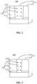
- FIG. 1 illustrates a flowchart of an exemplary hybrid wafer bonding method according to various embodiments of the present disclosure. Corresponding structures are illustrated in FIGS. 2-5 .
- the first semiconductor structure may include a first substrate, a first dielectric layer formed on the first substrate, and a first via structure formed in the first dielectric layer and on the first substrate.
- a corresponding structure is shown in FIG. 2 as an example.
- a first semiconductor structure 100 includes a first substrate 11, a first dielectric layer 122 formed on the first substrate 11, and a first via structure 123 formed in the first dielectric layer 122 and on the first substrate 11.
- the first substrate 11 may include a dielectric material, such as silicon oxide. Alternatively, the first substrate 11 may include any other suitable materials.
- the first semiconductor structure 100 may further include a first barrier film 121 on the first substrate 11.
- a first combination structure 12 may include a first barrier film 121, the first dielectric layer 122 on the first barrier film 121, and the first via structure 123 surrounded by the first dielectric layer 122 and the first barrier film 121.
- the first barrier film 121 may be a barrier film including a barrier material that blocks copper from diffusing, such as silicon nitride or nitrogen-doped silicon carbide (NDC), or any suitable material that blocks copper from diffusing.
- a barrier material that blocks copper from diffusing such as silicon nitride or nitrogen-doped silicon carbide (NDC), or any suitable material that blocks copper from diffusing.
- the first dielectric layer 122 may be a dielectric layer including a dielectric material, such as silicon oxide.
- the first via structure 123 may be a via that contain copper and metal impurities 1235. That is, the first via structure 123 may be a via that contains metal impurity-doped copper.
- a via may include conducting metal such as copper and include a portion inside a dielectric layer to form a path for conducting electrical currents.
- the first via structure 123 may be a first contact via that is to be in contact with and bonded with another contact via in the second semiconductor structure.
- the first via structure 123 may include one or more vias.
- the one or more vias may contain copper and metal impurities.
- the metal impurities may include at least one of Al, Mn, or Ag.
- the first combination structure 12 includes a first bonding surface 13.
- the first bonding surface 13 is a bonding surface that is to be bonded with another bonding surface in a second semiconductor structure for bonding the two surfaces and the two semiconductor structures.
- the first via structure 123 may include or may be a first contact via.
- the first bonding surface 13 includes a first contact via surface 131 of the first contact via and a first dielectric surface 132 in a same plane.
- the first contact via surface 131 is a surface of the first via structure 123 at one end of the first via structure 123, and the end of the first via structure 123 is to be bonded with the second semiconductor structure.
- the first dielectric surface 132 is a surface of the first dielectric layer 122 at one end of the first dielectric layer 122, and the end of the first dielectric layer 122 is to be bonded with the second semiconductor structure.
- the first contact via surface 131 is a top surface of the first via structure 123
- the first dielectric surface 132 is a top surface of the first dielectric layer 122.
- the first combination structure 12 may include a first barrier film 121, a first dielectric layer 122 on the first barrier film 121, and a first via structure 123, and the first via structure is surrounded by the first dielectric layer 122 and the first barrier film 121 at sides of the first via structure 123.
- a first combination structure may include a first dielectric layer and a first via structure, and the first via structure is surrounded by the first dielectric layer at sides of first via structure.
- forming a combination structure such as the first combination structure may include forming a barrier film, forming a dielectric layer, and forming a via in the dielectric layer or the dielectric layer and the barrier film, where the via contains metal impurity-doped copper.
- Forming a via containing copper doped with metal impurities (i.e., metal impurity-doped copper) in a dielectric layer such as a first dielectric layer may include forming a contact hole by etching in the dielectric layer, depositing a barrier layer on an inner surface of the contact hole, filling copper with metal impurities over the barrier layer in the contact hole to form the via.
- the barrier layer may be deposited on the inner surface of the contact hole to block copper from diffusing through the inner surface of the contact hole to the dielectric layer.
- the barrier layer may contain a barrier material that can block copper from diffusing, such as Ti, Ta, TiN, TaN, TiSiN or any combination thereof.
- Filling copper with metal impurities in the contact hole may include depositing a seed layer of metal impurity-doped copper over the barrier layer, electroplating copper in the contact hole, and smoothing a surface for the via and the dielectric layer.
- Depositing the seed layer of metal impurity-doped copper over the barrier layer may include sputtering a copper target and a target containing the metal impurities to deposit copper and the metal impurities to form the seed layer of metal impurity-doped copper by using a sputtering technique system, such as a magnetron sputtering system.
- CMP chemical-mechanical planarization
- the first via structure 123 may penetrate through the first dielectric layer and the first barrier film in the first combination structure. In other embodiments, a first via structure may not penetrate through the first dielectric layer and the first barrier film in the first combination structure. For example, a bottom of a first via structure may end inside the first dielectric layer.
- a second semiconductor structure is provided.
- the second semiconductor may include a second substrate, a second dielectric layer formed on the second substrate, and a second via structure formed in the second dielectric layer and on the second substrate.
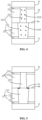
- a corresponding structure is shown in FIG. 3 as an example.
- a second semiconductor structure 200 includes a second substrate 21, a second dielectric layer 222 formed on the second substrate 21, and a second via structure 223 formed in the second dielectric layer 222 and on the second substrate 21.
- the second substrate 21 may include a dielectric material, such as silicon oxide. Alternatively, the second substrate 21 may include any other suitable materials.
- the second semiconductor structure may further include a second barrier film 221 on the second substrate 21.
- a second combination structure 22 may include a second barrier film 221, a second dielectric layer 222 on the second barrier film 221, and a second via structure 223 surrounded by the second dielectric layer 222 and the second barrier film 221.
- the second barrier film 221 may be a barrier film including a barrier material that blocks copper from diffusing, such as silicon nitride or NDC, or any suitable material that blocks copper from diffusing.
- the second dielectric layer 222 may be a dielectric layer including a dielectric material, such as silicon oxide.
- the second via structure 223 may be a via that contain copper and metal impurities 2235. That is, the second via structure 223 may be a via that contains metal impurity-doped copper.
- a via may include conducting metal such as copper and include a portion inside a dielectric layer to form a path for conducting electrical currents.
- the second via structure 223 may be a second contact via that is to be in contact with and bonded with the first contact via in the first semiconductor structure.
- the second via structure 223 may include one or more vias.
- the one or more vias may contain copper and metal impurities.
- the metal impurities may include at least one of Al, Mn, or Ag.
- the second combination structure 22 includes a second bonding surface 23.
- the second bonding surface 23 is a bonding surface that is to be bonded with a first bonding surface in the first semiconductor structure for bonding the two surfaces and the two wafers
- the second via structure 223 may include or may be a second contact via.
- the second bonding surface 23 includes a second contact via surface 231 of the second contact via and a second dielectric surface 232 in a same plane.
- the second contact via surface 231 is a surface of the second via structure 223 at one end of the second via structure 223, the end of the second via structure 223 is to be bonded with the first semiconductor structure.
- the second dielectric surface 232 is a surface of the second dielectric layer 222 at one end of the second dielectric layer 222, and the end of the second dielectric layer 222 is to be bonded with the first semiconductor structure.
- the second contact via surface 231 is a top surface of the second via structure 223, and the second dielectric surface 232 is a top surface of the second dielectric layer 222.
- the second combination structure 22 may include a second barrier film 221, a second dielectric layer 222 on the second barrier film 221, and a second via structure 223; and the second via structure 223 is surrounded by the second dielectric layer 222 and the second barrier film 221 at sides of the second via structure 223.
- a second combination structure may include a second dielectric layer and a second via structure; and the second via structure is surrounded by the second dielectric layer at sides of the second via structure.
- Forming the second combination structure is same as or similar to forming the first combination structure.
- forming a combination structure such as the second combination structure may include forming a barrier layer, forming a dielectric layer, and forming a via containing metal impurity-doped copper in the dielectric layer or in the dielectric layer and the barrier layer. References can be made to the above descriptions for forming the first combination structure.
- the second via structure 223 may penetrate through the second dielectric layer and the second barrier film in the second combination structure. In other embodiments, a second via structure may not penetrate through the second dielectric layer and the second barrier film in the second combination structure. For example, a bottom of the second via structure may end inside the second dielectric layer.
- the first contact via surface 131 may have a larger bonding area than the second contact via surface 231, and may cover the area of the second contact via surface 231 when the first contact via surface 131 and the second contact via surface 231 are bonded.
- the first contact via surface 131 may be a bonding surface of the first via structure 123
- the second contact via surface 231 may be a bonding surface of the second via structure 223, and the first contact via surface 131 may be larger than the second contact via surface 231.
- the first contact via surface 131 may have a larger area than the second contact via surface 231.
- the one or more vias in the first via structure 123 may contain copper and metal impurities.
- the one or more vias in the second via structure 223 may contain copper or contain copper and metal impurities.
- FIG. 4 illustrates a schematic structural diagram of an exemplary structure of hybrid wafer bonding according to various embodiments of the present disclosure.
- FIG. 5 illustrates a schematic structural diagram of another exemplary structure of hybrid wafer bonding according to various embodiments of the present disclosure.
- the first semiconductor structure is bonded with the second semiconductor structure by attaching the first contact via surface with the second contact via surface, where the second contact via surface and the first contact via surface have different surface areas and have an overlapped interface.
- a corresponding structure is shown in FIG. 4 as an example.
- the first semiconductor structure is bonded with the second semiconductor structure by attaching the first contact via surface with the second contact via surface, where the second contact via surface and the first contact via surface have different surface areas and have an overlapped interface.
- the first semiconductor structure and the second semiconductor structure may be oriented such that the first bonding surface 13 and the second bonding surface 23 face toward each other.
- the second semiconductor structure may be oriented upside down such that the second bonding surface is oriented downward to face toward the first bonding surface that is facing upward.
- the first semiconductor structure and the second semiconductor structure may be oriented in various manners, as long as the second bonding surface and the first bonding surface face toward each other.
- the first semiconductor structure may be oriented upside down such that the first bonding surface is oriented downward
- the second semiconductor structure may be oriented such that the second bonding surface faces upward. Accordingly, the first bonding surface and the second bonding surface oriented toward each other.
- first bonding surface and the second bonding surface are in direct contact with each other and bonded together.
- the second semiconductor structure is upside down, and the first semiconductor structure and the second semiconductor structure are bonded together.
- the first dielectric layer 122 is integrated with the second dielectric layer 222.
- the first via structure 123 is integrated with the second via structure 223 to form an integrated via structure 323.
- a bonding interface 30 is the interface formed at the location where the first bonding surface is in contact with the second bonding surface as the two semiconductor structures are bonded.
- the first via structure 123 and the second via structure 223 are conductive.
- An electrically conductive path is formed from the bottom to the top of the integrated via structure 323.
- a self-barrier layer is formed on a non-overlapped surface of one or more of the first and second contact via surfaces by an alloying process between the first semiconductor structure and the second semiconductor structure, where the self-barrier layer is formed by multi-component oxides corresponding to the metal impurities.
- a corresponding structure is shown in FIG. 5 as an example.
- a self-barrier layer 31 is formed on a non-overlapped surface of one or more of the first and second contact via surfaces by an alloying process between the first semiconductor structure and the second semiconductor structure.
- the self-barrier layer contains a multi-component oxide and blocks copper from diffusing to the dielectric layers.
- the alloying process between the first semiconductor structure and the second semiconductor structure may include annealing the first semiconductor structure and the second semiconductor structure to diffuse the metal impurities to the bonding interface to form the self-barrier layer that contains a multi-component oxide.
- the metal impurities may react with oxides at the interface to form the multi-component oxide.
- the alloying process may further include applying a pressure on one or more of the first semiconductor structure and the second semiconductor structure.
- the self-barrier layer 31 is on a non-overlapped surface of one or more of the first and second contact via surfaces.
- the self-barrier layer 31 corresponds to an orthogonal projection region at the bonding interface 30, referred to as a "self-barrier region.”
- the self-barrier region is an orthogonal projection of the self-barrier layer 31 on the plane of the bonding interface 30.
- the self-barrier region includes sub-regions that are within the first contact via surface and outside the second contact via surface and sub-regions that are outside the first contact via surface and within the second contact via surface.
- the self-barrier layer 31 contains the multi-component oxide that is formed by the oxide and one or more metal impurities in the bonded wafers, and hence eliminates the need to perform an extra deposition process for depositing a barrier layer at the bonding interface 30.
- the self-barrier region includes sub-regions that are within the first contact via surface and outside the second contact via surface.
- the self-barrier layer 31 may contain one or more multi-component oxides.
- the metal impurities in the first via structure and/or the second via structure may diffuse to the self-barrier region. Further, the metal impurities may react with the oxide in the dielectric layers at the bonding interface 30, e.g., the oxide in the second dielectric layer, to form a multi-component oxide in the self-barrier layer 31.
- the metal impurities in the vias may be at least one of Al, Mn, or Ag.
- the multi-component oxide may contain Si, O, and the at least one of Al, Mn, or Ag.
- the metal impurities may be Al, and the oxide may be silicon oxide, and the multi-component oxide may contain Al, Si, and O, such as Si x1 Al y1 O z1 (i.e., silicon aluminum oxide), where x1, y1, and z1 are suitable numbers.
- the metal impurities may be Mn
- the oxide may be silicon oxide
- the multi-component oxide may contain Mn, Si, and O, such as Si x2 Mn y2 O z2 , where x2, y2, and z2 are suitable numbers.
- the metal impurities may be Ag, and the oxide may be silicon oxide, and the multi-component oxide may contain Ag, Si, and O, such as Si x3 Ag y3 O z3 , where x3, y3, and z3 are suitable numbers.
- annealing the first semiconductor structure and the second semiconductor structure may include increasing the temperature of the first semiconductor structure and the second semiconductor structure and decreasing the temperature of the first semiconductor structure and the second semiconductor structure.
- annealing the first semiconductor structure and the second semiconductor structure may include increasing the temperature of the first semiconductor structure and the second semiconductor structure and decreasing slowly the temperature of the first semiconductor structure and the second semiconductor structure.
- annealing the first semiconductor structure and the second semiconductor structure may include increasing the temperature of the first semiconductor structure and the second semiconductor structure from an original temperature value to a predetermined temperature value, keeping the temperature of the first semiconductor structure and the second semiconductor structure at the predetermined temperature value for a predetermined time interval, and decreasing the temperature of the first semiconductor structure and the second semiconductor structure to the original temperature value.
- the original temperature value may be a temperature value of room temperature.
- the predetermined temperature value may be, for example, about 350 °C.
- the predetermined time interval may be, for example, approximately 120 minutes. That is, the temperature of the first semiconductor structure and the second semiconductor structure may be, for example, increased from an original temperature value to about 350 °C, and kept at about 350 °C for approximately 120 minutes, and decreased to the original temperature value.
- annealing the first semiconductor structure and the second semiconductor structure may include increasing the temperature of the first semiconductor structure and the second semiconductor structure from an original temperature value to a predetermined temperature value, keeping the temperature of the first semiconductor structure and the second semiconductor structure at the predetermined temperature value for a predetermined time interval, and decreasing the temperature of the first semiconductor structure and the second semiconductor structure to the original temperature value at a temperature reducing speed by using a temperature controller that includes a feedback control system.
- the predetermined temperature value, the predetermined time interval for keeping at the predetermined temperature value, and/or the temperature reducing speed may be determined according to properties associated with the multi-component oxide, the metal impurity, and/or the oxide in the second and first dielectric layers.
- the present disclosure provides another exemplary hybrid wafer bonding method.
- a first semiconductor structure 100' includes a first substrate 11, a first dielectric layer 122 formed on the first substrate 11, and a first via structure 123' formed in the first dielectric layer 122 and on the first substrate 11.
- the first via structure 123' includes a first switch element 1231 and a first contact via 1232.
- the first substrate 11 includes an insulating layer 111 and a conducting layer 112.
- the first semiconductor structure may further include a first barrier film 121 on the first substrate 11.
- a hole may be formed in the insulating layer 111 by etching and the conductive layer 112 may be formed in the hole.
- the conductive layer 112 is surrounded by the insulating layer 111 at sides of and a bottom of the conductive layer 112 and has a top exposed from the insulating layer 111.
- the conductive layer 112 may include a metal material such as copper.
- a barrier layer (not shown in FIG. 7 ) may be formed between the conductive layer 112 and the insulating layer 111 to block copper in the conductive layer 112 from diffusing into the insulating layer 111.
- a barrier layer may be deposited on inner surfaces of the hole formed in the insulating layer 111, e.g., an inner wall of the hole formed in the insulating layer 111 and a surface of the hole at one end of the hole, and further the conductive layer 112 is formed over the barrier layer.
- the barrier layer may contain a barrier material that can block copper from diffusing, such as Ti, Ta, TiN, TaN, TiSiN or any combination thereof.
- the first barrier film 121 may be a barrier film including a barrier material that blocks copper of the conductive layer 112 from diffusing, such as silicon nitride or NDC, or any suitable material that blocks copper from diffusing.
- a barrier material that blocks copper of the conductive layer 112 from diffusing such as silicon nitride or NDC, or any suitable material that blocks copper from diffusing.
- a first dielectric layer 122 may be formed on the first barrier film 121.
- the first dielectric layer 122 may be a dielectric layer that contains a dielectric material.
- the dielectric material may be silicon oxide.
- a first via structure 123' includes a first switch element 1231 and a first contact via 1232.
- the first combination structure 12 contains a first bonding surface, and the first switch element 1231 and the first contact via 1232 contain copper and metal impurities.
- a first switch element may be a via that penetrates the first dielectric layer and/or the first barrier film and is in contact with the first substrate.
- the first switch element may penetrate the first dielectric layer and/or the first barrier film by itself or together with one or more other vias, e.g., together with a first contact via.
- a contact hole may be formed in the first barrier film 121 and the first dielectric layer 122 by etching.
- the contact hole may include a groove on the first substrate and a trench connected to and on the groove.
- the groove extends from the first dielectric layer 122 to a bottom of the first barrier film 121 to be in contact with the first substrate.
- the trench is connected to and on the groove.
- the trench extends from a top of the first dielectric layer 122 to a depth in the first dielectric layer 122.
- the trench has a larger lateral dimension than the groove.
- the first switch element 1231 may be formed in the groove and the first contact via 1232 may be formed in contact with the first switch element 1231 and in the trench.
- the first switch element 1231 may be formed penetrating the first barrier film 121 between the first substrate 11 and the first dielectric layer 122 and on the conductive layer 112.
- An orthogonal projection of the first contact via 1232 on the first substrate 11 is greater than an orthogonal projection of the first switch element 1231 on the first substrate 11 in area.
- a barrier layer may be deposited over inner surfaces of the groove and the trench, e.g., the inner walls of the groove and inner walls and surfaces 1233 of the trench at an end of the trench.
- the barrier layer may contain a barrier material that can block copper from diffusing, such as Ti, Ta, TiN, TaN, TiSiN or any combination thereof.
- a first switch element 1231 is formed in the groove and the first contact via 1232 is formed in the trench by introducing copper doped with metal impurities 1235.
- the metal impurities 1235 may include at least one of Al, Mn, or Ag.
- One end of the first switch element 1231 is connected to the first contact via 1232 .
- Another end of the first switch element 1231 is connected to the conductive layer 112.
- the first via structure 123' includes the first switch element 1231 and the first contact via 1232.
- the first combination structure 12 may include the first barrier film 121, the first dielectric layer 122, and the first via structure 123'.
- the first combination structure 12 contains the first bonding surface 13.
- the first bonding surface 13 includes a first contact via surface 131 and a first dielectric surface 132 in a same plane.
- the first contact via surface 131 may be a surface of the first contact via 1232 and a surface of the first via structure 123'.
- the first contact via surface 131 is a surface of the first via structure 123' at one end of the first via structure 123', and the end of the first via structure 123' is to be bonded with the second semiconductor structure.
- the first dielectric surface 132 is a surface of the first dielectric layer 122 at one end of the first dielectric layer 122, and the end of the first dielectric layer 122 is to be bonded with the second semiconductor structure.
- the first contact via surface 131 is a top surface of the first via structure 123' and a top surface of the first contact via 1232
- the first dielectric surface 132 is a top surface of the first dielectric layer 122.
- a second semiconductor structure where a second via structure includes a second switch element and a second contact via.
- the second semiconductor may include a second substrate, a second dielectric layer formed on the second substrate, and a second via structure formed in the second dielectric layer and on the second substrate, where a second via structure may include a second switch element and a second contact via.
- a corresponding structure is shown in FIG. 8 as an example.
- a second semiconductor structure 200' includes a second substrate 21, a second dielectric layer 222 formed on the second substrate 21, and a second via structure 223' formed in the second dielectric layer 222 and on the second substrate 21.
- the second via structure 223' includes a second switch element 2231 and a second contact via 2232.
- the second substrate 21 includes an insulating layer 211 and a conducting layer 212.
- the second semiconductor structure may further include a second barrier film 221 on the second substrate 21.
- a second combination structure 22 may include the second via structure 223' and the second dielectric layer 222.
- the second combination structure 22 may further include the second barrier film 221.
- the insulating layer 211 may include an insulating material such as silicon oxide.
- a hole may be formed in the insulating layer 211 by etching and the conductive layer 212 may be formed in the hole.
- the conductive layer 212 is surrounded by the insulating layer 211 at sides of and a bottom of the conductive layer 212 and has a top exposed from the insulating layer 211.
- the second substrate 21 includes the insulating layer 211 and the conductive layer 212.
- the conductive layer 212 may include a metal material such as copper.
- a barrier layer (not shown in FIG. 8 ) may be formed between the conductive layer 212 and the insulating layer 211 to block copper in the conductive layer 212 from diffusing to the insulating layer 211.
- a barrier layer may be deposited on inner surfaces of the hole formed in the insulating layer 211, e.g., inner walls and an end, e.g., a bottom, of the hole formed in the insulating layer 211, and further the conductive layer 212 is formed over the barrier layer.
- a second barrier film 221 may be deposited on the second substrate 21.
- the second barrier film 221 may be a barrier film including a barrier material that blocks copper in the conductive layer 212 from diffusing, such as silicon nitride or NDC, or any suitable material that blocks copper from diffusing.
- a barrier material that blocks copper in the conductive layer 212 from diffusing such as silicon nitride or NDC, or any suitable material that blocks copper from diffusing.
- a second dielectric layer 222 may be formed on the second barrier film 221.
- the second dielectric layer 222 may be a dielectric layer that contains a dielectric material.
- the dielectric material may be silicon oxide.
- a second via structure 223' includes a second switch element 2231 and a second contact via 2232.
- the second combination structure 22 contains the second bonding surface 23.
- the second switch element 2231 and the second contact via 2232 contain copper, or copper and metal impurities 2235.
- a second switch element may be a via that penetrates the second dielectric layer and/or the second barrier film and is in contact with the second substrate.
- the second switch element may penetrate the second dielectric layer and/or the second barrier film by itself or together with one or more other vias, e.g., together with a second contact via.
- a contact hole may be formed in the second barrier film 221 and the second dielectric layer 222 by etching.
- the contact hole may include a groove on the second substrate 21 and a trench connected to and on the groove.
- the groove extends from the second dielectric layer 222 to a bottom of the second barrier film 221 to be in contact with the second substrate 21.
- the trench is connected to and on the groove.
- the trench extends from a top of the second dielectric layer 222 to a depth in the second dielectric layer 222.
- the trench has a larger lateral dimension than the groove.
- the second switch element 2231 may be formed in the groove and the second contact via 2232 may be formed in contact with the second switch element and in the trench.
- the second switch element may be formed penetrating the second barrier film between the second substrate and the second dielectric layer and on the conductive layer
- a barrier layer may be deposited over inner surfaces of the groove and the trench, e.g., the inner walls of the groove and inner walls and surfaces 2233 of the trench at one end of the trench.
- the barrier layer may contain a barrier material that can block copper from diffusing, such as Ti, Ta, TiN, TaN, TiSiN or any combination thereof.
- a second switch element 2231 is formed in the groove and a second contact via 2232 is formed in the trench by introducing copper doped with metal impurities 2235.
- the metal impurities may include at least one of Al, Mn, or Ag.
- One end of the second switch element 2231 is connected to the second contact via 2232.
- Another end of the second switch element 2231 is connected to the conductive layer 212.
- the second via structure 223' includes the second switch element 2231 and the second contact via 2232.
- the second combination structure 22 includes the second barrier film 221, the second dielectric layer 222, and the second via structure 223'.
- the second combination structure 22 contains the second bonding surface 23.
- the second bonding surface 23 includes a second contact via surface 231 and a second dielectric surface 232 in a same plane.
- the second contact via surface 231 may be a surface of the second contact via 2232 and a surface of the second via structure 223'.
- the second contact via surface 231 is a surface of the second via structure 223' at one end of the second via structure 223', and the end of the second via structure 223' is to be bonded with the first semiconductor structure.
- the second dielectric surface 232 is a surface of the second dielectric layer 222 at one end of the second dielectric layer 222, and the end of the second dielectric layer 222 is to be bonded with the first semiconductor structure.
- the second contact via surface 231 is a top surface of the second via structure 223' and a top surface of the second contact via 2232
- the second dielectric surface 232 is a top surface of the second dielectric layer 222.
- the first contact via surface 131 has a larger area than the second contact via surface 231.
- the first semiconductor structure is bonded with the second semiconductor structure by attaching the first contact via surface with the second contact via surface, where the second contact via surface and the first contact via surface have different surface areas and have an overlapped interface.
- a corresponding structure is shown in FIG. 9 as an example.
- the first semiconductor structure is bonded with the second semiconductor structure by attaching the first contact via surface with the second contact via surface, where the second contact via surface and the first contact via surface have different surface areas and have an overlapped interface.
- the second semiconductor structure is arranged upside down as compared to the orientation of the second semiconductor structure in FIG. 8 , and the first semiconductor structure and the second semiconductor structure are bonded together.
- the first dielectric layer 122 is integrated with the second dielectric layer 222, and the first via structure 123' is integrated with the second via structure 223' to form an integrated via structure.
- the first via structure 123' and the second via structure 223' are conductive.
- the conductive layer 112 is electrically connected to the conductive layer 212 by the first via structure 123' and the second via structure 223'. That is, the conductive layer 112 is electrically connected to the conductive layer 212 by an electrically conductive path that includes the first switch element 1231, the first contact via 1232, the second contact via 2232, and the second switch element 2231.
- a bonding interface 30 is the interface formed at the location where the first bonding surface is in contact with the second bonding surface as the two semiconductor structures are bonded.
- a self-barrier layer is formed on a non-overlapped surface of one or more of the first and second contact via surfaces by an alloying process between the first semiconductor structure and the second semiconductor structure, where the self-barrier layer is formed by one or more multi-component oxides corresponding to the metal impurities.
- a corresponding structure is shown in FIG. 10 as an example.
- a self-barrier layer 31 is formed on a non-overlapped surface of one or more of the first and second contact via surfaces by an alloying process between the first semiconductor structure and the second semiconductor structure.
- the self-barrier layer contains a multi-component oxide and blocks copper from diffusing to the dielectric layers.
- the alloying process between the first semiconductor structure and the second semiconductor structure may include annealing the first semiconductor structure and the second semiconductor structure to diffuse the metal impurities to the bonding interface to form the self-barrier layer that contains a multi-component oxide.
- the metal impurities may react with the oxide at the interface to form the multi-component oxide.
- the self-barrier layer that contains the multi-component oxide blocks copper from diffusing to the dielectric layers, i.e., the first dielectric layer and the second dielectric layer.
- the alloying process may further include applying a pressure on one or more of the first semiconductor structure and the second semiconductor structure.
- the self-barrier layer 31 is formed in a region at the bonding interface 30.
- the self-barrier layer 31 corresponds to an orthogonal projection region at the bonding interface, referred to as a "self-barrier region.”
- the self-barrier region is an orthogonal projection of the self-barrier layer 31 on the plane of the bonding interface 30.
- the self-barrier region includes sub-regions that are within the first contact via surface and outside the second contact via surface and sub-regions that are outside the first contact via surface and within the second contact via surface.
- the self-barrier layer 31 may contain one or more multi-component oxides.
- the metal impurities in the first via structure and/or the second via structure may diffuse to the self-barrier region. Further, the metal impurities may react with the oxide in the dielectric layers at the bonding interface 30, e.g., the oxide in the second dielectric layer, to form a multi-component oxide.
- the multi-component oxide may contain Si, O, and at least one of Al, Mn, or Ag.
- the metal impurities may be Al, and the oxide may be silicon oxide, and the multi-component oxide may contain Al, Si, and O., such as Si x1 Al y1 O z1 , where x1, y1, and z1 are suitable numbers.
- the metal impurities may be Mn
- the oxide may be silicon oxide
- the multi-component oxide may contain Mn, Si, and O, such as Si x2 Mn y2 O z2 , where x2, y2, and z2 are suitable numbers.
- the metal impurities may be Ag, and the oxide may be silicon oxide, and the multi-component oxide may contain Ag, Si, and O, such as Si x3 Ag y3 O z3 , where x3, y3, and z3 are suitable numbers.
- the present disclosure provides a wafer structure of hybrid bonding.
- the structure contains bonded semiconductor structures and a self-barrier layer that contains a multi-component oxide and blocks copper from diffusing to a dielectric layer in the structure.
- FIG. 5 illustrates an exemplary structure of hybrid wafer bonding.
- the structure of hybrid wafer bonding includes a first semiconductor structure, a second semiconductor structure, and a self-barrier layer.
- the first via structure 123 may include a via.
- a via may include conducting metal such as copper and include portions inside a dielectric layer to form a path for conducting electrical currents.
- the second combination structure 22 includes a second dielectric layer 222, a second barrier film 221 on the second dielectric layer 222, a second via structure 223 surrounded by the second dielectric layer 222 and the second barrier film 221.
- the first via structure 123 includes a first contact via surface that is at one end of the first via structure 123 and the end of the first via structure 123 is bonded with the second semiconductor structure.
- the second via structure 223 includes a second contact via surface that is a surface of the second via structure 223 at one end of the second via structure 223 and the end of the second via structure 223 is bonded with the first semiconductor structure.
- the self-barrier layer 31 is formed in a region at the bonding interface 30.
- the self-barrier layer 31 corresponds to an orthogonal projection region at the bonding interface 30, referred to as a "self-barrier region.”
- the self-barrier region is an orthogonal projection of the self-barrier layer 31 on the plane of the bonding interface 30.
- the self-barrier region may include sub-regions that are within the first contact via surface and outside the second contact via surface and sub-regions that are outside the first contact via surface and within the second contact via surface.
- the self-barrier layer 31 may contain one or more multi-component oxides.
- the metal impurities in the first via structure and/or the second via structure may diffuse to the self-barrier region. Further, the metal impurities may react with the oxide in the dielectric layer at the bonding interface 30, e.g., the oxide in the second dielectric layer, to form a multi-component oxide in the self-barrier layer 31.
- the metal impurities in the vias may be at least one of Al, Mn, or Ag.
- the multi-component oxide may contain Si, O, and the at least one of Al, Mn, or Ag.
- the metal impurities in the vias may be Al, and the oxide may be silicon oxide, and the multi-component oxide may contain Al, Si and O, such as Si x1 Al y1 O z1 , where x1, y1, and z1 are suitable numbers.
- the self-barrier layer 31 that contains a multi-component oxide and blocks copper from diffusing to the dielectric layers across the bonding interface 30.
- Barrier layers deposited over the inner surfaces of the contact holes in the first dielectric layer 122 and the second dielectric layer 222, such as the inner walls of the contact holes in the first dielectric layer 122 and the second dielectric layer 222, may block copper from diffusing to the dielectric layers through the inner surfaces of the contact holes.
- the present disclosure provides another structure of hybrid wafer bonding.
- the structure may include bonded semiconductor structure and a self-barrier layer that contains a multi-component oxide and blocks copper from diffusing to the dielectric layer.
- FIG. 10 illustrates another structure of hybrid wafer bonding according to various embodiments of the present disclosure.
- the structure of hybrid wafer bonding includes a first semiconductor structure, a second semiconductor structure, and a self-barrier layer.
- the structure of hybrid wafer bonding includes a first substrate 11, a first combination structure 12 on the first substrate, a second combination structure 22 on the first combination structure 12, and a second substrate 21 on the second combination structure 22, a bonding interface 30, and a self-barrier layer 31.
- the bonding interface 30 is formed at the boundary where the second combination structure 22 and the first combination structure 12 are in contact with each other.
- the first substrate 11 includes an insulating layer 111 and a conductive layer 112 in the insulating layer 111.
- the conductive layer 112 is surrounded by the insulating layer 111 at sides of and a bottom of the conductive layer 112 and has a top exposed from the insulating layer 111.
- the first combination structure 12 includes a first barrier film 121 on the first substrate 11, a first dielectric layer 122 on the first barrier film 121, and a first via structure 123' surrounded by the first dielectric layer 122 and the first barrier film 121.
- the first via structure 123' includes a first switch element 1231 and a first contact via 1232 in contact with one end of the first switch element 1231.
- the first switch element 1231 has another end in contact with the conductive layer 112.
- a via may include conducting metal such as copper and include portions inside a dielectric layer to form a path for conducting electrical currents.
- the second combination structure 22 includes a second dielectric layer 222, a second barrier film 221 on the second dielectric layer 222, and a second via structure 223' surrounded by the second dielectric layer 222 and the second barrier film 221.
- the second via structure 223' includes a second contact via 2232 and a second switch element 2231 having one end in contact with the second contact via 2232.
- the second switch element 2231 has another end in contact with the conductive layer 212 of the second substrate 21.
- the first via structure 123' includes a first contact via surface that is a surface of the first via structure 123' at one end of the first via structure 123' and the end of the first via structure 123' is bonded with the second semiconductor structure.
- the second via structure 223' includes a second contact via surface that is a surface of the second via structure 223' at one end of the second via structure 223' and the end of the second via structure 223' is bonded with the first semiconductor structure.
- the self-barrier layer 31 is formed in a region at the bonding interface 30.
- the self-barrier layer 31 corresponds to an orthogonal projection region at the bonding interface 30, referred to as a "self-barrier region.”
- the self-barrier region is an orthogonal projection of the self-barrier layer 31 on the plane of the bonding interface 30.
- the self-barrier region includes sub-regions that are within the first contact via surface and outside the second contact via surface and sub-regions that are outside the first contact via surface and within the second contact via surface.
- the self-barrier layer 31 may contain one or more multi-component oxides.
- the metal impurities in the first via structure and/or the second via structure may diffuse to the self-barrier region. Further, the metal impurities may react with the oxide in the dielectric layer at the bonding interface 30, e.g., the oxide in the second dielectric layer, to form a multi-component oxide in the self-barrier layer 31.
- the metal impurities in the vias may be at least one of Al, Mn, or Ag.
- the multi-component oxide may contain Si, O, and the least one of Al, Mn, or Ag.
- the metal impurities may be Al, and the oxide may be silicon oxide, and the multi-component oxide may contain Al, Si, and O, such as Si x1 Al y1 O z1 , where x1, y1, and z1 are suitable numbers.
- the self-barrier layer 31 contains a multi-component oxide and blocks copper from diffusing to the dielectric layers.
- Barrier layers deposited over the inner surfaces of the contact holes in the first dielectric layer 122 and the second dielectric layer 222 can block copper from diffusing to the dielectric layers through the inner surfaces of the contact holes.
- the inner surfaces of the contact hole in the first dielectric layer 122 and the first barrier film 121 may include the inner walls and the surfaces 1233 of the contact hole in the first dielectric layer 122.
- the contact hole may include a groove on the first substrate and a trench connected to and on the groove.
- the surfaces 1233 of the contact hole in the first dielectric layer 122 is at one end of the trench and is outside the groove laterally. The end of the trench is closer to the groove in the first dielectric layer 122 than the bonding interface 30.
- the inner surfaces of the contact hole in the second dielectric layer 222 and the second barrier film 221 may include the inner walls and the surfaces 2233 of the contact hole in the second dielectric layer 222.
- the contact hole may include a groove on the second substrate and a trench connected to and on the groove.
- the surfaces 2233 of the contact hole in the second dielectric layer 222 is at one end of the trench and is outside the groove laterally. The end of the trench is closer to the groove in the second dielectric layer 222 than the bonding interface 30.
- the self-barrier layer 31 may block copper from diffusing through the bonding interface 30 to the dielectric layers including the integrated first dielectric layer 122 and second dielectric layer 222. Diffusion of copper through the bonding interface is prevented without the need to deposit barrier layers on the bonding surfaces.
- barrier layers deposited on the inner surfaces of the contact holes in the dielectric layers may block copper from diffusing through the inner surfaces of the contact holes to the dielectric layers.
- the barrier layer may contain a barrier material that can block copper from diffusing, such as Ti, Ta, TiN, TaN, TiSiN or any combination thereof.
- the conductive layer 112 and the conductive layer 212 may contain copper.
- the first barrier film 121 may block copper in the conductive layer 112 from diffusing to the dielectric layers including the integrated first dielectric layer 122 and second dielectric layer 222.
- Barrier layers (not shown in FIG. 10 ) may be deposited in the hole in the insulating layer 111 and further the conductive layer is formed in the hole over the barrier layers to fill the hole. Barrier layers may block copper in the conductive layer 112 from diffusing to the insulating layer 111 through the sides and the end of the conductive layer 112 facing the insulating layer 111.
- the barrier layer may contain a barrier material that can block copper from diffusing, such as Ti, Ta, TiN, TaN, TiSiN or any combination thereof.
- the second barrier film 221 may block copper in the conductive layer 212 from diffusing to the dielectric layers including the integrated first dielectric layer 122 and second dielectric layer 222.
- Barrier layers (not shown in FIG. 10 ) may be deposited over the hole in the insulating layer 211 and further the conductive layer 212 is formed in the hole over the barrier layers to fill the hole.
- the barrier layers may block copper in the conductive layer 212 from diffusing to the insulating layer 211 through the sides and the end of the conductive layer 212 facing the insulating layer 211.
- the barrier layer may contain a barrier material that can block copper from diffusing, such as Ti, Ta, TiN, TaN, TiSiN or any combination thereof.
- the self-barrier region of the self-barrier layer 31 at the bonding interface 30 may have various shapes according to actual application scenarios.
- the shape of the self-barrier region of the self-barrier layer 31 may vary according to the first contact via surface 131 and the second contact via surface 231. That is, the shape of the self-barrier region may vary according to the via surface of the first semiconductor structure and the via surface of the second semiconductor structure that are bonded together at the bonding interface.
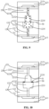
- FIG. 11 illustrates an exemplary orthogonal projection region of self-barrier layer according to various embodiments of the present disclosure.
- the orthogonal projection region of self-barrier layer refers to the self-barrier region described in method embodiments.
- the first contact via surface 131 has a circle shape.
- the second contact via surface 231 has a circle shape, and has a smaller area than the first contact via surface 131.
- the first contact via surface 131 and the second contact via surface 231 are concentric at the bonding interface.
- the second contact via surface 231 is located within the first contact via surface 131 at the bonding interface. That is, an orthogonal projection of the first contact via surface 131 on the bonding interface completely covers an orthogonal projection of the second contact via surface 231 on the bonding interface.
- the self-barrier region 331 is in the hatched area that is inside the first contact via surface 131 and outside the second contact via surface 231.
- the self-barrier region 331 has an annular shape, where annular ring sizes of the shape have the same value.
- An annular ring size is a width of self-barrier region 331 in a radial direction pointing from the center of the smaller one of the first and second contact via surfaces, e.g., the second contact via surface 231.
- the inner circle and the outer circle of the self-barrier region 331 are concentric.
- one or more vias in the first via structure 123 may include metal impurity-doped copper, and one or more vias the second via structure 223 may include copper.
- the metal impurities in the one or more vias in the first via structure 123 may diffuse to the bonding interface 30 to react with the oxide in the second dielectric layer to form the self-barrier layer 31 in the self-barrier region 331.
- one or more vias in the first via structure 123 may include metal impurity-doped copper
- one or more vias in the second via structure 223 may include metal impurity-doped copper.
- the metal impurities in the one or more vias in the first via structure 123 and the second via structure 223 may diffuse to the bonding interface 30 to react with the oxide in the second dielectric layer to form the self-barrier layer 31 in the self-barrier region 331.
- FIG. 12 illustrates another exemplary orthogonal projection region of self-barrier layer according to various embodiments of the present disclosure.
- a first contact via surface 131' has a circle shape.
- the second contact via surface 231' has a circle shape and has a smaller area than the first contact via surface 131'.
- the first contact via surface 131' and the second contact via surface 231' are non-concentric at the bonding interfere. That is, the center of the first contact via surface 131' is at a different location with respect to the center of the second contact via surface 231' at the bonding interfere.
- the second contact via surface 231' is located within the first contact via surface 131' at the bonding interface. That is, an orthogonal projection of the first contact via surface 131' on the bonding interface completely covers an orthogonal projection of the second contact via surface 231' on the bonding interface.
- the self-barrier region 331' is in the hatched area that is inside the first contact via surface 131' and outside the second contact via surface 231'.
- the self-barrier region 331' has an irregular annular shape with annular ring sizes having different values, where a annular ring size is a width of self-barrier region 331' in a radial direction pointing from the center of the smaller one of the first and second contact via surfaces, e.g., the second contact via surface 231'.
- the inner circle and the outer circle of the self-barrier region 331' are non-concentric.
- one or more vias in the first via structure may include metal impurity-doped copper, and one or more vias the second via structure may include copper.
- the metal impurities in the one or more vias in the first via structure may diffuse to the bonding interface to react with the oxide in the second dielectric layer to form the self-barrier layer 31 in the self-barrier region.
- one or more vias in the first via structure may include metal impurity-doped copper
- one or more vias in the second via structure may include metal impurity-doped copper.
- the metal impurities in the one or more vias in the first via structure and the second via structure may diffuse to the bonding interface to react with the oxide in the second dielectric layer to form the self-barrier layer 31 in the self-barrier region.
- the first contact via surface may have various shapes, such as a circle shape, an ellipse shape, a square shape, a rectangle shape, or any other suitable shape.
- the second contact via surface may have various shapes, such as a circle shape, an ellipse shape, a square shape, a rectangle shape, or any other suitable shape.
- a center of the first contact via surface and a center of the second contact via surface may be at the same location or at different locations when two semiconductor structures are bonded.
Landscapes
- Internal Circuitry In Semiconductor Integrated Circuit Devices (AREA)
- Wire Bonding (AREA)
Abstract
Description
- This application relates to the field of wafer bonding technologies and, more particularly, to a hybrid wafer bonding method and a structure thereof.
- In a hybrid wafer bonding process, semiconductor structures having contact vias may be bonded together. However, the contact vias often have different sizes. This may result in interactions between a surface portion of a contact via of one semiconductor structure and a dielectric layer of the other semiconductor structure. For example, copper in the contact via may diffuse into the dielectric layer and degrade the quality of bonded wafers.
- Conventional solutions for blocking metal diffusion include depositing a metal blocking layer on the bonding surface of each wafer. The metal blocking layer and the dielectric layer are made of different materials. When forming the contact via, an etch process may be performed on the metal blocking layer and the dielectric layer. Due to different etching rates, gaps may be formed between the metal blocking layer and the dielectric layer. Consequently, defects may occur in the contact via.
- The disclosed methods and structures are directed to solve one or more problems set forth above and other problems.
- One aspect of the present disclosure includes a hybrid wafer bonding method. The method includes providing a first semiconductor structure and providing a second semiconductor. The first semiconductor structure includes a first substrate, a first dielectric layer formed on the first substrate, and a first via structure formed in the first dielectric layer and on the first substrate. The first via structure includes a first contact via and first metal impurities doped in the first contact via, the first contact via having a first contact via surface. The second semiconductor structure includes a second substrate, a second dielectric layer formed on the second substrate, and a second via structure formed in the second dielectric layer and on the second substrate. The second via structure includes a second contact via and second metal impurities doped in the second contact via, the second contact via having a second contact via surface. The method further includes bonding the first semiconductor structure with the second semiconductor structure by attaching the first contact via surface with the second contact via surface, wherein the second contact via surface and the first contact via surface have different surface areas and have an overlapped interface; and forming a self-barrier layer on a non-overlapped surface of one or more of the first and second contact via surfaces by an alloying process between the first semiconductor structure and the second semiconductor structure, wherein the self-barrier layer is formed by a multi-component oxide corresponding to the first and second metal impurities.
- Another aspect of the present disclosure includes a hybrid wafer bonding structure including a first semiconductor structure, a second semiconductor structure, and a self-barrier layer. The first semiconductor structure includes a first substrate, a first dielectric layer formed on the first substrate, and a first via structure formed in the first dielectric layer and on the first substrate, the first contact via having a first contact surface. The second semiconductor structure includes a second substrate, a second dielectric layer formed on the second substrate, and a second via structure formed in the second dielectric layer and on the second substrate, the second contact via having a second contact via surface. The first semiconductor structure is bonded with the second semiconductor structure, the first contact via surface is attached with the second contact via surface, and the second contact via surface and the first contact via surface have different surface areas and have an overlapped interface. The self-barrier layer is formed on a non-overlapped surface of one or more of the first and second contact via surfaces at a bonding interface between the first and second semiconductor structures, wherein the self-barrier layer contains a multi-component oxide.
- Other aspects of the present disclosure can be understood by those skilled in the art in light of the description, the claims, and the drawings of the present disclosure.
- The following drawings are merely examples for illustrative purposes according to various disclosed embodiments and are not intended to limit the scope of the present disclosure.
-
FIG. 1 illustrates an exemplary hybrid wafer bonding method according to various embodiments of the present disclosure. -
FIG. 2 illustrates an exemplary first semiconductor structure according to various embodiments of the present disclosure. -
FIG. 3 illustrates an exemplary second semiconductor structure according to various embodiments of the present disclosure. -
FIG. 4 illustrates an exemplary structure of hybrid wafer bonding according to various embodiments of the present disclosure. -
FIG. 5 illustrates another exemplary structure of hybrid wafer bonding according to various embodiments of the present disclosure. -
FIG. 6 illustrates another exemplary hybrid wafer bonding method according to various embodiments of the present disclosure. -
FIG. 7 illustrates another exemplary first semiconductor structure according to various embodiments of the present disclosure. -
FIG. 8 illustrates another exemplary second semiconductor structure according to various embodiments of the present disclosure. -
FIG. 9 illustrates another structure of hybrid wafer bonding according to various embodiments of the present disclosure. -
FIG. 10 illustrates another structure of hybrid wafer bonding according to various embodiments of the present disclosure. -
FIG. 11 illustrates an exemplary orthogonal projection region of a self-barrier layer according to various embodiments of the present disclosure. -
FIG. 12 illustrates another exemplary orthogonal projection region of a self-barrier layer according to various embodiments of the present disclosure. - The following describes the technical solutions in the embodiments of the present invention with reference to the accompanying drawings. Wherever possible, the same reference numbers will be used throughout the drawings to refer to the same or like parts. Apparently, the described embodiments are merely some but not all the embodiments of the present invention. Other embodiments obtained by a person skilled in the art based on the embodiments of the present invention without creative efforts shall fall within the protection scope of the present disclosure.
- The hybrid wafer bonding method includes providing a first semiconductor structure and a second semiconductor structure, and bonding the first semiconductor structure with the second semiconductor structure to form a self-barrier layer that contains a multi-component oxide.
-
FIG. 1 illustrates a flowchart of an exemplary hybrid wafer bonding method according to various embodiments of the present disclosure. Corresponding structures are illustrated inFIGS. 2-5 . - In S110 of
FIG. 1 , a first semiconductor structure is provided. The first semiconductor structure may include a first substrate, a first dielectric layer formed on the first substrate, and a first via structure formed in the first dielectric layer and on the first substrate. A corresponding structure is shown inFIG. 2 as an example. - Referring to
FIG. 2 , afirst semiconductor structure 100 includes afirst substrate 11, a firstdielectric layer 122 formed on thefirst substrate 11, and afirst via structure 123 formed in the firstdielectric layer 122 and on thefirst substrate 11. - The
first substrate 11 may include a dielectric material, such as silicon oxide. Alternatively, thefirst substrate 11 may include any other suitable materials. - Referring to
FIG. 2 , thefirst semiconductor structure 100 may further include afirst barrier film 121 on thefirst substrate 11. Afirst combination structure 12 may include afirst barrier film 121, the firstdielectric layer 122 on thefirst barrier film 121, and thefirst via structure 123 surrounded by the firstdielectric layer 122 and thefirst barrier film 121. - The
first barrier film 121 may be a barrier film including a barrier material that blocks copper from diffusing, such as silicon nitride or nitrogen-doped silicon carbide (NDC), or any suitable material that blocks copper from diffusing. - The first
dielectric layer 122 may be a dielectric layer including a dielectric material, such as silicon oxide. - In some embodiments, referring to
FIG. 2 , thefirst via structure 123 may be a via that contain copper andmetal impurities 1235. That is, thefirst via structure 123 may be a via that contains metal impurity-doped copper. A via may include conducting metal such as copper and include a portion inside a dielectric layer to form a path for conducting electrical currents. - In some embodiments, the
first via structure 123 may be a first contact via that is to be in contact with and bonded with another contact via in the second semiconductor structure. - In some embodiments, the
first via structure 123 may include one or more vias. - In some embodiments, the one or more vias may contain copper and metal impurities. The metal impurities may include at least one of Al, Mn, or Ag.
- The
first combination structure 12 includes a first bonding surface 13. The first bonding surface 13 is a bonding surface that is to be bonded with another bonding surface in a second semiconductor structure for bonding the two surfaces and the two semiconductor structures. - In some embodiments, the first via
structure 123 may include or may be a first contact via. The first bonding surface 13 includes a first contact viasurface 131 of the first contact via and a firstdielectric surface 132 in a same plane. The first contact viasurface 131 is a surface of the first viastructure 123 at one end of the first viastructure 123, and the end of the first viastructure 123 is to be bonded with the second semiconductor structure. The firstdielectric surface 132 is a surface of thefirst dielectric layer 122 at one end of thefirst dielectric layer 122, and the end of thefirst dielectric layer 122 is to be bonded with the second semiconductor structure. In the orientation shown inFIG. 2 , the first contact viasurface 131 is a top surface of the first viastructure 123, and the firstdielectric surface 132 is a top surface of thefirst dielectric layer 122. - In some embodiments, the
first combination structure 12 may include afirst barrier film 121, a firstdielectric layer 122 on thefirst barrier film 121, and a first viastructure 123, and the first via structure is surrounded by thefirst dielectric layer 122 and thefirst barrier film 121 at sides of the first viastructure 123. In other embodiments, a first combination structure may include a first dielectric layer and a first via structure, and the first via structure is surrounded by the first dielectric layer at sides of first via structure. - In some embodiments, forming a combination structure such as the first combination structure may include forming a barrier film, forming a dielectric layer, and forming a via in the dielectric layer or the dielectric layer and the barrier film, where the via contains metal impurity-doped copper.
- Forming a via containing copper doped with metal impurities (i.e., metal impurity-doped copper) in a dielectric layer such as a first dielectric layer may include forming a contact hole by etching in the dielectric layer, depositing a barrier layer on an inner surface of the contact hole, filling copper with metal impurities over the barrier layer in the contact hole to form the via. The barrier layer may be deposited on the inner surface of the contact hole to block copper from diffusing through the inner surface of the contact hole to the dielectric layer. The barrier layer may contain a barrier material that can block copper from diffusing, such as Ti, Ta, TiN, TaN, TiSiN or any combination thereof. Filling copper with metal impurities in the contact hole may include depositing a seed layer of metal impurity-doped copper over the barrier layer, electroplating copper in the contact hole, and smoothing a surface for the via and the dielectric layer. Depositing the seed layer of metal impurity-doped copper over the barrier layer may include sputtering a copper target and a target containing the metal impurities to deposit copper and the metal impurities to form the seed layer of metal impurity-doped copper by using a sputtering technique system, such as a magnetron sputtering system. After depositing a seed layer of metal impurity-doped copper over the barrier layer and electroplating copper in the contact hole, excess metal impurity-doped copper and copper may be introduced outside the contact hole, a surface for the via and the dielectric layer may be smoothed to remove the excess metal impurity-doped copper and copper and to obtain a smooth surface. The surface for the via and the dielectric layer may be smoothed by chemical-mechanical planarization (CMP).
- In some embodiments, the first via
structure 123 may penetrate through the first dielectric layer and the first barrier film in the first combination structure. In other embodiments, a first via structure may not penetrate through the first dielectric layer and the first barrier film in the first combination structure. For example, a bottom of a first via structure may end inside the first dielectric layer. - In S120 of
FIG. 1 , a second semiconductor structure is provided. The second semiconductor may include a second substrate, a second dielectric layer formed on the second substrate, and a second via structure formed in the second dielectric layer and on the second substrate. A corresponding structure is shown inFIG. 3 as an example. - Referring to
FIG. 3 , asecond semiconductor structure 200 includes asecond substrate 21, asecond dielectric layer 222 formed on thesecond substrate 21, and a second viastructure 223 formed in thesecond dielectric layer 222 and on thesecond substrate 21. - The
second substrate 21 may include a dielectric material, such as silicon oxide. Alternatively, thesecond substrate 21 may include any other suitable materials. - Referring to
FIG. 3 , the second semiconductor structure may further include asecond barrier film 221 on thesecond substrate 21. Asecond combination structure 22 may include asecond barrier film 221, asecond dielectric layer 222 on thesecond barrier film 221, and a second viastructure 223 surrounded by thesecond dielectric layer 222 and thesecond barrier film 221. - The
second barrier film 221 may be a barrier film including a barrier material that blocks copper from diffusing, such as silicon nitride or NDC, or any suitable material that blocks copper from diffusing. - The
second dielectric layer 222 may be a dielectric layer including a dielectric material, such as silicon oxide. - In some embodiments, referring to
FIG. 3 , the second viastructure 223 may be a via that contain copper andmetal impurities 2235. That is, the second viastructure 223 may be a via that contains metal impurity-doped copper. A via may include conducting metal such as copper and include a portion inside a dielectric layer to form a path for conducting electrical currents. - In some embodiments, the second via
structure 223 may be a second contact via that is to be in contact with and bonded with the first contact via in the first semiconductor structure. - In some embodiments, the second via
structure 223 may include one or more vias. - In some embodiments, the one or more vias may contain copper and metal impurities. The metal impurities may include at least one of Al, Mn, or Ag.
- The
second combination structure 22 includes a second bonding surface 23. The second bonding surface 23 is a bonding surface that is to be bonded with a first bonding surface in the first semiconductor structure for bonding the two surfaces and the two wafers - In some embodiments, the second via
structure 223 may include or may be a second contact via. The second bonding surface 23 includes a second contact viasurface 231 of the second contact via and a seconddielectric surface 232 in a same plane. The second contact viasurface 231 is a surface of the second viastructure 223 at one end of the second viastructure 223, the end of the second viastructure 223 is to be bonded with the first semiconductor structure. The seconddielectric surface 232 is a surface of thesecond dielectric layer 222 at one end of thesecond dielectric layer 222, and the end of thesecond dielectric layer 222 is to be bonded with the first semiconductor structure. In the orientation shown inFIG. 3 , the second contact viasurface 231 is a top surface of the second viastructure 223, and the seconddielectric surface 232 is a top surface of thesecond dielectric layer 222. - In some embodiments, the
second combination structure 22 may include asecond barrier film 221, asecond dielectric layer 222 on thesecond barrier film 221, and a second viastructure 223; and the second viastructure 223 is surrounded by thesecond dielectric layer 222 and thesecond barrier film 221 at sides of the second viastructure 223. In other embodiments, a second combination structure may include a second dielectric layer and a second via structure; and the second via structure is surrounded by the second dielectric layer at sides of the second via structure. - Forming the second combination structure is same as or similar to forming the first combination structure. In some embodiments, forming a combination structure such as the second combination structure may include forming a barrier layer, forming a dielectric layer, and forming a via containing metal impurity-doped copper in the dielectric layer or in the dielectric layer and the barrier layer. References can be made to the above descriptions for forming the first combination structure.
- In some embodiments, the second via
structure 223 may penetrate through the second dielectric layer and the second barrier film in the second combination structure. In other embodiments, a second via structure may not penetrate through the second dielectric layer and the second barrier film in the second combination structure. For example, a bottom of the second via structure may end inside the second dielectric layer. - In some embodiments, the first contact via
surface 131 may have a larger bonding area than the second contact viasurface 231, and may cover the area of the second contact viasurface 231 when the first contact viasurface 131 and the second contact viasurface 231 are bonded. In other words, the first contact viasurface 131 may be a bonding surface of the first viastructure 123, and the second contact viasurface 231 may be a bonding surface of the second viastructure 223, and the first contact viasurface 131 may be larger than the second contact viasurface 231. - In some embodiments, the first contact via
surface 131 may have a larger area than the second contact viasurface 231. The one or more vias in the first viastructure 123 may contain copper and metal impurities. The one or more vias in the second viastructure 223 may contain copper or contain copper and metal impurities. -
FIG. 4 illustrates a schematic structural diagram of an exemplary structure of hybrid wafer bonding according to various embodiments of the present disclosure.FIG. 5 illustrates a schematic structural diagram of another exemplary structure of hybrid wafer bonding according to various embodiments of the present disclosure. - In S130 of
FIG. 1 , the first semiconductor structure is bonded with the second semiconductor structure by attaching the first contact via surface with the second contact via surface, where the second contact via surface and the first contact via surface have different surface areas and have an overlapped interface. A corresponding structure is shown inFIG. 4 as an example. - Referring to
FIG. 4 , the first semiconductor structure is bonded with the second semiconductor structure by attaching the first contact via surface with the second contact via surface, where the second contact via surface and the first contact via surface have different surface areas and have an overlapped interface. - In some embodiments, the first semiconductor structure and the second semiconductor structure may be oriented such that the first bonding surface 13 and the second bonding surface 23 face toward each other. For example, the second semiconductor structure may be oriented upside down such that the second bonding surface is oriented downward to face toward the first bonding surface that is facing upward.
- The first semiconductor structure and the second semiconductor structure may be oriented in various manners, as long as the second bonding surface and the first bonding surface face toward each other. For example, the first semiconductor structure may be oriented upside down such that the first bonding surface is oriented downward, and the second semiconductor structure may be oriented such that the second bonding surface faces upward. Accordingly, the first bonding surface and the second bonding surface oriented toward each other.
- Further, the first bonding surface and the second bonding surface are in direct contact with each other and bonded together. Referring to
FIG. 4 , the second semiconductor structure is upside down, and the first semiconductor structure and the second semiconductor structure are bonded together. Thefirst dielectric layer 122 is integrated with thesecond dielectric layer 222. The first viastructure 123 is integrated with the second viastructure 223 to form an integrated viastructure 323. - A
bonding interface 30 is the interface formed at the location where the first bonding surface is in contact with the second bonding surface as the two semiconductor structures are bonded. - The first via
structure 123 and the second viastructure 223 are conductive. An electrically conductive path is formed from the bottom to the top of the integrated viastructure 323. - In S140 of
FIG. 1 , a self-barrier layer is formed on a non-overlapped surface of one or more of the first and second contact via surfaces by an alloying process between the first semiconductor structure and the second semiconductor structure, where the self-barrier layer is formed by multi-component oxides corresponding to the metal impurities. A corresponding structure is shown inFIG. 5 as an example. - Referring to
FIG. 5 , a self-barrier layer 31 is formed on a non-overlapped surface of one or more of the first and second contact via surfaces by an alloying process between the first semiconductor structure and the second semiconductor structure. The self-barrier layer contains a multi-component oxide and blocks copper from diffusing to the dielectric layers. - In some embodiments, the alloying process between the first semiconductor structure and the second semiconductor structure may include annealing the first semiconductor structure and the second semiconductor structure to diffuse the metal impurities to the bonding interface to form the self-barrier layer that contains a multi-component oxide. The metal impurities may react with oxides at the interface to form the multi-component oxide. The self-barrier layer that contains the multi-component oxide that blocks copper from diffusing to the dielectric layers, i.e., the first dielectric layer and the second dielectric layer.
- In some embodiments, the alloying process may further include applying a pressure on one or more of the first semiconductor structure and the second semiconductor structure.
- The self-
barrier layer 31 is on a non-overlapped surface of one or more of the first and second contact via surfaces. The self-barrier layer 31 corresponds to an orthogonal projection region at thebonding interface 30, referred to as a "self-barrier region." The self-barrier region is an orthogonal projection of the self-barrier layer 31 on the plane of thebonding interface 30. The self-barrier region includes sub-regions that are within the first contact via surface and outside the second contact via surface and sub-regions that are outside the first contact via surface and within the second contact via surface. - The self-
barrier layer 31 contains the multi-component oxide that is formed by the oxide and one or more metal impurities in the bonded wafers, and hence eliminates the need to perform an extra deposition process for depositing a barrier layer at thebonding interface 30. - In the exemplary scenarios that the first contact via surface covers the second contact via surface, sub-regions that are outside the first contact via surface and within the second contact via surface do not exist and the self-barrier region includes sub-regions that are within the first contact via surface and outside the second contact via surface.
- The self-
barrier layer 31 may contain one or more multi-component oxides. During the annealing process, the metal impurities in the first via structure and/or the second via structure may diffuse to the self-barrier region. Further, the metal impurities may react with the oxide in the dielectric layers at thebonding interface 30, e.g., the oxide in the second dielectric layer, to form a multi-component oxide in the self-barrier layer 31. - The metal impurities in the vias may be at least one of Al, Mn, or Ag. The multi-component oxide may contain Si, O, and the at least one of Al, Mn, or Ag.
- In some embodiments, the metal impurities may be Al, and the oxide may be silicon oxide, and the multi-component oxide may contain Al, Si, and O, such as Six1Aly1Oz1 (i.e., silicon aluminum oxide), where x1, y1, and z1 are suitable numbers.
- In some embodiments, the metal impurities may be Mn, and the oxide may be silicon oxide, and the multi-component oxide may contain Mn, Si, and O, such as Six2Mny2Oz2, where x2, y2, and z2 are suitable numbers.
- In some embodiments, the metal impurities may be Ag, and the oxide may be silicon oxide, and the multi-component oxide may contain Ag, Si, and O, such as Six3Agy3Oz3, where x3, y3, and z3 are suitable numbers.
- In some embodiments, annealing the first semiconductor structure and the second semiconductor structure may include increasing the temperature of the first semiconductor structure and the second semiconductor structure and decreasing the temperature of the first semiconductor structure and the second semiconductor structure.
- In some embodiments, annealing the first semiconductor structure and the second semiconductor structure may include increasing the temperature of the first semiconductor structure and the second semiconductor structure and decreasing slowly the temperature of the first semiconductor structure and the second semiconductor structure.
- In some embodiments, annealing the first semiconductor structure and the second semiconductor structure may include increasing the temperature of the first semiconductor structure and the second semiconductor structure from an original temperature value to a predetermined temperature value, keeping the temperature of the first semiconductor structure and the second semiconductor structure at the predetermined temperature value for a predetermined time interval, and decreasing the temperature of the first semiconductor structure and the second semiconductor structure to the original temperature value. The original temperature value may be a temperature value of room temperature.
- The predetermined temperature value may be, for example, about 350 °C. The predetermined time interval may be, for example, approximately 120 minutes. That is, the temperature of the first semiconductor structure and the second semiconductor structure may be, for example, increased from an original temperature value to about 350 °C, and kept at about 350 °C for approximately 120 minutes, and decreased to the original temperature value.
- In some embodiments, annealing the first semiconductor structure and the second semiconductor structure may include increasing the temperature of the first semiconductor structure and the second semiconductor structure from an original temperature value to a predetermined temperature value, keeping the temperature of the first semiconductor structure and the second semiconductor structure at the predetermined temperature value for a predetermined time interval, and decreasing the temperature of the first semiconductor structure and the second semiconductor structure to the original temperature value at a temperature reducing speed by using a temperature controller that includes a feedback control system. The predetermined temperature value, the predetermined time interval for keeping at the predetermined temperature value, and/or the temperature reducing speed may be determined according to properties associated with the multi-component oxide, the metal impurity, and/or the oxide in the second and first dielectric layers.
- The present disclosure provides another exemplary hybrid wafer bonding method.
-
FIG. 6 illustrates another exemplary hybrid wafer bonding method according to various embodiments of the present disclosure. Corresponding structure are illustrated inFIGS. 7-10 . For processes of the exemplary hybrid wafer bonding method illustrated inFIG. 6 including S110', S120', S130', and S140', references can be made to the above descriptions of processes of the one or more exemplary methods such as the method described in connection withFIG. 1 , including S110, S120, S130, and S140. - In S110' of
FIG. 6 , a first semiconductor structure is provided, where a first via structure includes a first switch element and a first contact via. The first semiconductor structure may include a first substrate, a first dielectric layer formed on the first substrate, and a first via structure formed in the first dielectric layer and on the first substrate, where the first via structure may include a first switch element and a first contact via. A corresponding structure is shown inFIG. 7 as an example. - Referring to
FIG. 7 , a first semiconductor structure 100' includes afirst substrate 11, a firstdielectric layer 122 formed on thefirst substrate 11, and a first via structure 123' formed in thefirst dielectric layer 122 and on thefirst substrate 11. The first via structure 123' includes afirst switch element 1231 and a first contact via 1232. Thefirst substrate 11 includes an insulating layer 111 and a conducting layer 112. The first semiconductor structure may further include afirst barrier film 121 on thefirst substrate 11. - A
first combination structure 12 may include the first via structure 123', thefirst dielectric layer 122. Thefirst combination structure 12 may further include thefirst barrier film 121. - The insulating layer 111 may include an insulating material. In some embodiments, the insulating material may be silicon oxide.
- In some embodiments, a hole may be formed in the insulating layer 111 by etching and the conductive layer 112 may be formed in the hole. The conductive layer 112 is surrounded by the insulating layer 111 at sides of and a bottom of the conductive layer 112 and has a top exposed from the insulating layer 111.
- In some embodiments, the conductive layer 112 may include a metal material such as copper. Further, a barrier layer (not shown in
FIG. 7 ) may be formed between the conductive layer 112 and the insulating layer 111 to block copper in the conductive layer 112 from diffusing into the insulating layer 111. For example, a barrier layer may be deposited on inner surfaces of the hole formed in the insulating layer 111, e.g., an inner wall of the hole formed in the insulating layer 111 and a surface of the hole at one end of the hole, and further the conductive layer 112 is formed over the barrier layer. The barrier layer may contain a barrier material that can block copper from diffusing, such as Ti, Ta, TiN, TaN, TiSiN or any combination thereof. - In some embodiments, referring to
FIG. 7 , thefirst barrier film 121 may be a barrier film including a barrier material that blocks copper of the conductive layer 112 from diffusing, such as silicon nitride or NDC, or any suitable material that blocks copper from diffusing. - A
first dielectric layer 122 may be formed on thefirst barrier film 121. - In some embodiments, the
first dielectric layer 122 may be a dielectric layer that contains a dielectric material. The dielectric material may be silicon oxide. - A first via structure 123' includes a
first switch element 1231 and a first contact via 1232. Thefirst combination structure 12 contains a first bonding surface, and thefirst switch element 1231 and the first contact via 1232 contain copper and metal impurities. - In some embodiments, a first switch element may be a via that penetrates the first dielectric layer and/or the first barrier film and is in contact with the first substrate. The first switch element may penetrate the first dielectric layer and/or the first barrier film by itself or together with one or more other vias, e.g., together with a first contact via.
- A contact hole may be formed in the
first barrier film 121 and thefirst dielectric layer 122 by etching. The contact hole may include a groove on the first substrate and a trench connected to and on the groove. The groove extends from thefirst dielectric layer 122 to a bottom of thefirst barrier film 121 to be in contact with the first substrate. The trench is connected to and on the groove. The trench extends from a top of thefirst dielectric layer 122 to a depth in thefirst dielectric layer 122. The trench has a larger lateral dimension than the groove. - The
first switch element 1231 may be formed in the groove and the first contact via 1232 may be formed in contact with thefirst switch element 1231 and in the trench. Thefirst switch element 1231 may be formed penetrating thefirst barrier film 121 between thefirst substrate 11 and thefirst dielectric layer 122 and on the conductive layer 112. - An orthogonal projection of the first contact via 1232 on the
first substrate 11 is greater than an orthogonal projection of thefirst switch element 1231 on thefirst substrate 11 in area. - In some embodiments, a barrier layer may be deposited over inner surfaces of the groove and the trench, e.g., the inner walls of the groove and inner walls and surfaces 1233 of the trench at an end of the trench. The barrier layer may contain a barrier material that can block copper from diffusing, such as Ti, Ta, TiN, TaN, TiSiN or any combination thereof.
- Further, a
first switch element 1231 is formed in the groove and the first contact via 1232 is formed in the trench by introducing copper doped withmetal impurities 1235. Themetal impurities 1235 may include at least one of Al, Mn, or Ag. One end of thefirst switch element 1231 is connected to the first contact via 1232 . Another end of thefirst switch element 1231 is connected to the conductive layer 112. - The first via structure 123' includes the
first switch element 1231 and the first contact via 1232. Thefirst combination structure 12 may include thefirst barrier film 121, thefirst dielectric layer 122, and the first via structure 123'. - The
first combination structure 12 contains the first bonding surface 13. The first bonding surface 13 includes a first contact viasurface 131 and a firstdielectric surface 132 in a same plane. In some embodiments, the first contact viasurface 131 may be a surface of the first contact via 1232 and a surface of the first via structure 123'. - The first contact via
surface 131 is a surface of the first via structure 123' at one end of the first via structure 123', and the end of the first via structure 123' is to be bonded with the second semiconductor structure. The firstdielectric surface 132 is a surface of thefirst dielectric layer 122 at one end of thefirst dielectric layer 122, and the end of thefirst dielectric layer 122 is to be bonded with the second semiconductor structure. In the orientation shown inFIG. 7 , the first contact viasurface 131 is a top surface of the first via structure 123' and a top surface of the first contact via 1232, and the firstdielectric surface 132 is a top surface of thefirst dielectric layer 122. - In S120' of
FIG. 6 , a second semiconductor structure is provided, where a second via structure includes a second switch element and a second contact via. The second semiconductor may include a second substrate, a second dielectric layer formed on the second substrate, and a second via structure formed in the second dielectric layer and on the second substrate, where a second via structure may include a second switch element and a second contact via. A corresponding structure is shown inFIG. 8 as an example. - Referring to
FIG. 8 , a second semiconductor structure 200' includes asecond substrate 21, asecond dielectric layer 222 formed on thesecond substrate 21, and a second via structure 223' formed in thesecond dielectric layer 222 and on thesecond substrate 21. The second via structure 223' includes asecond switch element 2231 and a second contact via 2232. Thesecond substrate 21 includes an insulatinglayer 211 and aconducting layer 212. The second semiconductor structure may further include asecond barrier film 221 on thesecond substrate 21. - A
second combination structure 22 may include the second via structure 223' and thesecond dielectric layer 222. Thesecond combination structure 22 may further include thesecond barrier film 221. - In some embodiments, referring to
FIG. 8 , the insulatinglayer 211 may include an insulating material such as silicon oxide. - In some embodiments, a hole may be formed in the insulating
layer 211 by etching and theconductive layer 212 may be formed in the hole. Theconductive layer 212 is surrounded by the insulatinglayer 211 at sides of and a bottom of theconductive layer 212 and has a top exposed from the insulatinglayer 211. Thesecond substrate 21 includes the insulatinglayer 211 and theconductive layer 212. - In some embodiments, the
conductive layer 212 may include a metal material such as copper. Further, a barrier layer (not shown inFIG. 8 ) may be formed between theconductive layer 212 and the insulatinglayer 211 to block copper in theconductive layer 212 from diffusing to the insulatinglayer 211. For example, a barrier layer may be deposited on inner surfaces of the hole formed in the insulatinglayer 211, e.g., inner walls and an end, e.g., a bottom, of the hole formed in the insulatinglayer 211, and further theconductive layer 212 is formed over the barrier layer. - A
second barrier film 221 may be deposited on thesecond substrate 21. - In some embodiments, referring to
FIG. 8 , thesecond barrier film 221 may be a barrier film including a barrier material that blocks copper in theconductive layer 212 from diffusing, such as silicon nitride or NDC, or any suitable material that blocks copper from diffusing. - A
second dielectric layer 222 may be formed on thesecond barrier film 221. - In some embodiments, the
second dielectric layer 222 may be a dielectric layer that contains a dielectric material. The dielectric material may be silicon oxide. - A second via structure 223' includes a
second switch element 2231 and a second contact via 2232. Thesecond combination structure 22 contains the second bonding surface 23. Thesecond switch element 2231 and the second contact via 2232 contain copper, or copper andmetal impurities 2235. - In some embodiments, a second switch element may be a via that penetrates the second dielectric layer and/or the second barrier film and is in contact with the second substrate. The second switch element may penetrate the second dielectric layer and/or the second barrier film by itself or together with one or more other vias, e.g., together with a second contact via.
- A contact hole may be formed in the
second barrier film 221 and thesecond dielectric layer 222 by etching. The contact hole may include a groove on thesecond substrate 21 and a trench connected to and on the groove. The groove extends from thesecond dielectric layer 222 to a bottom of thesecond barrier film 221 to be in contact with thesecond substrate 21. The trench is connected to and on the groove. The trench extends from a top of thesecond dielectric layer 222 to a depth in thesecond dielectric layer 222. The trench has a larger lateral dimension than the groove. - The
second switch element 2231 may be formed in the groove and the second contact via 2232 may be formed in contact with the second switch element and in the trench. The second switch element may be formed penetrating the second barrier film between the second substrate and the second dielectric layer and on the conductive layer - In some embodiments, a barrier layer may be deposited over inner surfaces of the groove and the trench, e.g., the inner walls of the groove and inner walls and surfaces 2233 of the trench at one end of the trench. The barrier layer may contain a barrier material that can block copper from diffusing, such as Ti, Ta, TiN, TaN, TiSiN or any combination thereof.
- Further, a
second switch element 2231 is formed in the groove and a second contact via 2232 is formed in the trench by introducing copper doped withmetal impurities 2235. The metal impurities may include at least one of Al, Mn, or Ag. One end of thesecond switch element 2231 is connected to the second contact via 2232. Another end of thesecond switch element 2231 is connected to theconductive layer 212. - The second via structure 223' includes the
second switch element 2231 and the second contact via 2232. Thesecond combination structure 22 includes thesecond barrier film 221, thesecond dielectric layer 222, and the second via structure 223'. - The
second combination structure 22 contains the second bonding surface 23. The second bonding surface 23 includes a second contact viasurface 231 and a seconddielectric surface 232 in a same plane. In some embodiments, the second contact viasurface 231 may be a surface of the second contact via 2232 and a surface of the second via structure 223'. - The second contact via
surface 231 is a surface of the second via structure 223' at one end of the second via structure 223', and the end of the second via structure 223' is to be bonded with the first semiconductor structure. The seconddielectric surface 232 is a surface of thesecond dielectric layer 222 at one end of thesecond dielectric layer 222, and the end of thesecond dielectric layer 222 is to be bonded with the first semiconductor structure. In the orientation shown inFIG. 8 , the second contact viasurface 231 is a top surface of the second via structure 223' and a top surface of the second contact via 2232, and the seconddielectric surface 232 is a top surface of thesecond dielectric layer 222. - In some embodiments, the first contact via
surface 131 has a larger area than the second contact viasurface 231. - In S130' of
FIG. 6 , the first semiconductor structure is bonded with the second semiconductor structure by attaching the first contact via surface with the second contact via surface, where the second contact via surface and the first contact via surface have different surface areas and have an overlapped interface. A corresponding structure is shown inFIG. 9 as an example. - Referring to
FIG. 9 , the first semiconductor structure is bonded with the second semiconductor structure by attaching the first contact via surface with the second contact via surface, where the second contact via surface and the first contact via surface have different surface areas and have an overlapped interface. The second semiconductor structure is arranged upside down as compared to the orientation of the second semiconductor structure inFIG. 8 , and the first semiconductor structure and the second semiconductor structure are bonded together. Thefirst dielectric layer 122 is integrated with thesecond dielectric layer 222, and the first via structure 123' is integrated with the second via structure 223' to form an integrated via structure. - The first via structure 123' and the second via structure 223' are conductive. Thus, the conductive layer 112 is electrically connected to the
conductive layer 212 by the first via structure 123' and the second via structure 223'. That is, the conductive layer 112 is electrically connected to theconductive layer 212 by an electrically conductive path that includes thefirst switch element 1231, the first contact via 1232, the second contact via 2232, and thesecond switch element 2231. - A
bonding interface 30 is the interface formed at the location where the first bonding surface is in contact with the second bonding surface as the two semiconductor structures are bonded. - In S140' of
FIG. 6 , a self-barrier layer is formed on a non-overlapped surface of one or more of the first and second contact via surfaces by an alloying process between the first semiconductor structure and the second semiconductor structure, where the self-barrier layer is formed by one or more multi-component oxides corresponding to the metal impurities. A corresponding structure is shown inFIG. 10 as an example. - Referring to
FIG. 10 , a self-barrier layer 31 is formed on a non-overlapped surface of one or more of the first and second contact via surfaces by an alloying process between the first semiconductor structure and the second semiconductor structure. The self-barrier layer contains a multi-component oxide and blocks copper from diffusing to the dielectric layers. - In some embodiments, the alloying process between the first semiconductor structure and the second semiconductor structure may include annealing the first semiconductor structure and the second semiconductor structure to diffuse the metal impurities to the bonding interface to form the self-barrier layer that contains a multi-component oxide. The metal impurities may react with the oxide at the interface to form the multi-component oxide. The self-barrier layer that contains the multi-component oxide blocks copper from diffusing to the dielectric layers, i.e., the first dielectric layer and the second dielectric layer.
- In some embodiments, the alloying process may further include applying a pressure on one or more of the first semiconductor structure and the second semiconductor structure.
- Referring to
FIG. 10 , the self-barrier layer 31 is formed in a region at thebonding interface 30. The self-barrier layer 31 corresponds to an orthogonal projection region at the bonding interface, referred to as a "self-barrier region." The self-barrier region is an orthogonal projection of the self-barrier layer 31 on the plane of thebonding interface 30. The self-barrier region includes sub-regions that are within the first contact via surface and outside the second contact via surface and sub-regions that are outside the first contact via surface and within the second contact via surface. - The self-
barrier layer 31 may contain one or more multi-component oxides. During the annealing process, the metal impurities in the first via structure and/or the second via structure may diffuse to the self-barrier region. Further, the metal impurities may react with the oxide in the dielectric layers at thebonding interface 30, e.g., the oxide in the second dielectric layer, to form a multi-component oxide. - The multi-component oxide may contain Si, O, and at least one of Al, Mn, or Ag.
- In some embodiments, the metal impurities may be Al, and the oxide may be silicon oxide, and the multi-component oxide may contain Al, Si, and O., such as Six1Aly1Oz1, where x1, y1, and z1 are suitable numbers.
- In some embodiments, the metal impurities may be Mn, and the oxide may be silicon oxide, and the multi-component oxide may contain Mn, Si, and O, such as Six2Mny2Oz2, where x2, y2, and z2 are suitable numbers.
- In some embodiments, the metal impurities may be Ag, and the oxide may be silicon oxide, and the multi-component oxide may contain Ag, Si, and O, such as Six3Agy3Oz3, where x3, y3, and z3 are suitable numbers.
- The present disclosure provides a wafer structure of hybrid bonding. The structure contains bonded semiconductor structures and a self-barrier layer that contains a multi-component oxide and blocks copper from diffusing to a dielectric layer in the structure.
-
FIG. 5 illustrates an exemplary structure of hybrid wafer bonding. - The structure of hybrid wafer bonding includes a first semiconductor structure, a second semiconductor structure, and a self-barrier layer.
- Specifically, the structure of hybrid wafer bonding includes a
first substrate 11, afirst combination structure 12 on the first substrate, asecond combination structure 22 on thefirst combination structure 12, and asecond substrate 21 on thesecond combination structure 22, abonding interface 30, and a self-barrier layer 31. Thebonding interface 30 is formed at the boundary where thesecond combination structure 22 and the first combination structure are in contact with each other. - The
first combination structure 12 includes afirst barrier film 121 on thefirst substrate 11, a firstdielectric layer 122 on thefirst barrier film 121, and a first viastructure 123 surrounded by thefirst dielectric layer 122 and thefirst barrier film 121. - In some embodiments, the first via
structure 123 may include a via. A via may include conducting metal such as copper and include portions inside a dielectric layer to form a path for conducting electrical currents. - Referring to
FIG. 5 , thesecond combination structure 22 includes asecond dielectric layer 222, asecond barrier film 221 on thesecond dielectric layer 222, a second viastructure 223 surrounded by thesecond dielectric layer 222 and thesecond barrier film 221. - The first via
structure 123 includes a first contact via surface that is at one end of the first viastructure 123 and the end of the first viastructure 123 is bonded with the second semiconductor structure. The second viastructure 223 includes a second contact via surface that is a surface of the second viastructure 223 at one end of the second viastructure 223 and the end of the second viastructure 223 is bonded with the first semiconductor structure. - The self-
barrier layer 31 is formed in a region at thebonding interface 30. The self-barrier layer 31 corresponds to an orthogonal projection region at thebonding interface 30, referred to as a "self-barrier region." The self-barrier region is an orthogonal projection of the self-barrier layer 31 on the plane of thebonding interface 30. The self-barrier region may include sub-regions that are within the first contact via surface and outside the second contact via surface and sub-regions that are outside the first contact via surface and within the second contact via surface. - For the exemplary structure of hybrid wafer bonding, references can be made to the descriptions for method embodiments.
- The self-
barrier layer 31 may contain one or more multi-component oxides. During the annealing process, the metal impurities in the first via structure and/or the second via structure may diffuse to the self-barrier region. Further, the metal impurities may react with the oxide in the dielectric layer at thebonding interface 30, e.g., the oxide in the second dielectric layer, to form a multi-component oxide in the self-barrier layer 31. - The metal impurities in the vias may be at least one of Al, Mn, or Ag. The multi-component oxide may contain Si, O, and the at least one of Al, Mn, or Ag. For example, the metal impurities in the vias may be Al, and the oxide may be silicon oxide, and the multi-component oxide may contain Al, Si and O, such as Six1Aly1Oz1, where x1, y1, and z1 are suitable numbers.
- The self-
barrier layer 31 that contains a multi-component oxide and blocks copper from diffusing to the dielectric layers across thebonding interface 30. Barrier layers deposited over the inner surfaces of the contact holes in thefirst dielectric layer 122 and thesecond dielectric layer 222, such as the inner walls of the contact holes in thefirst dielectric layer 122 and thesecond dielectric layer 222, may block copper from diffusing to the dielectric layers through the inner surfaces of the contact holes. - The present disclosure provides another structure of hybrid wafer bonding. The structure may include bonded semiconductor structure and a self-barrier layer that contains a multi-component oxide and blocks copper from diffusing to the dielectric layer.
-
FIG. 10 illustrates another structure of hybrid wafer bonding according to various embodiments of the present disclosure. - The structure of hybrid wafer bonding includes a first semiconductor structure, a second semiconductor structure, and a self-barrier layer.
- Specifically, the structure of hybrid wafer bonding includes a
first substrate 11, afirst combination structure 12 on the first substrate, asecond combination structure 22 on thefirst combination structure 12, and asecond substrate 21 on thesecond combination structure 22, abonding interface 30, and a self-barrier layer 31. Thebonding interface 30 is formed at the boundary where thesecond combination structure 22 and thefirst combination structure 12 are in contact with each other. - The
first substrate 11 includes an insulating layer 111 and a conductive layer 112 in the insulating layer 111. The conductive layer 112 is surrounded by the insulating layer 111 at sides of and a bottom of the conductive layer 112 and has a top exposed from the insulating layer 111. - The
first combination structure 12 includes afirst barrier film 121 on thefirst substrate 11, a firstdielectric layer 122 on thefirst barrier film 121, and a first via structure 123' surrounded by thefirst dielectric layer 122 and thefirst barrier film 121. - The first via structure 123' includes a
first switch element 1231 and a first contact via 1232 in contact with one end of thefirst switch element 1231. Thefirst switch element 1231 has another end in contact with the conductive layer 112. A via may include conducting metal such as copper and include portions inside a dielectric layer to form a path for conducting electrical currents. - The
second combination structure 22 includes asecond dielectric layer 222, asecond barrier film 221 on thesecond dielectric layer 222, and a second via structure 223' surrounded by thesecond dielectric layer 222 and thesecond barrier film 221. - The second via structure 223' includes a second contact via 2232 and a
second switch element 2231 having one end in contact with the second contact via 2232. Thesecond switch element 2231 has another end in contact with theconductive layer 212 of thesecond substrate 21. - The first via structure 123' includes a first contact via surface that is a surface of the first via structure 123' at one end of the first via structure 123' and the end of the first via structure 123' is bonded with the second semiconductor structure. The second via structure 223' includes a second contact via surface that is a surface of the second via structure 223' at one end of the second via structure 223' and the end of the second via structure 223' is bonded with the first semiconductor structure.
- The self-
barrier layer 31 is formed in a region at thebonding interface 30. The self-barrier layer 31 corresponds to an orthogonal projection region at thebonding interface 30, referred to as a "self-barrier region." The self-barrier region is an orthogonal projection of the self-barrier layer 31 on the plane of thebonding interface 30. The self-barrier region includes sub-regions that are within the first contact via surface and outside the second contact via surface and sub-regions that are outside the first contact via surface and within the second contact via surface. - For the self-barrier region, references can be made to the descriptions for method embodiments.
- The self-
barrier layer 31 may contain one or more multi-component oxides. During the annealing process, the metal impurities in the first via structure and/or the second via structure may diffuse to the self-barrier region. Further, the metal impurities may react with the oxide in the dielectric layer at thebonding interface 30, e.g., the oxide in the second dielectric layer, to form a multi-component oxide in the self-barrier layer 31. - The metal impurities in the vias may be at least one of Al, Mn, or Ag. The multi-component oxide may contain Si, O, and the least one of Al, Mn, or Ag. For example, the metal impurities may be Al, and the oxide may be silicon oxide, and the multi-component oxide may contain Al, Si, and O, such as Six1Aly1Oz1, where x1, y1, and z1 are suitable numbers.
- The self-
barrier layer 31 contains a multi-component oxide and blocks copper from diffusing to the dielectric layers. Barrier layers deposited over the inner surfaces of the contact holes in thefirst dielectric layer 122 and thesecond dielectric layer 222 can block copper from diffusing to the dielectric layers through the inner surfaces of the contact holes. - In some embodiments, the inner surfaces of the contact hole in the
first dielectric layer 122 and thefirst barrier film 121 may include the inner walls and thesurfaces 1233 of the contact hole in thefirst dielectric layer 122. The contact hole may include a groove on the first substrate and a trench connected to and on the groove. Thesurfaces 1233 of the contact hole in thefirst dielectric layer 122 is at one end of the trench and is outside the groove laterally. The end of the trench is closer to the groove in thefirst dielectric layer 122 than thebonding interface 30. - In some embodiments, the inner surfaces of the contact hole in the
second dielectric layer 222 and thesecond barrier film 221 may include the inner walls and thesurfaces 2233 of the contact hole in thesecond dielectric layer 222. The contact hole may include a groove on the second substrate and a trench connected to and on the groove. Thesurfaces 2233 of the contact hole in thesecond dielectric layer 222 is at one end of the trench and is outside the groove laterally. The end of the trench is closer to the groove in thesecond dielectric layer 222 than thebonding interface 30. - In some embodiments, the self-
barrier layer 31 may block copper from diffusing through thebonding interface 30 to the dielectric layers including the integrated firstdielectric layer 122 and seconddielectric layer 222. Diffusion of copper through the bonding interface is prevented without the need to deposit barrier layers on the bonding surfaces. - In some embodiments, barrier layers deposited on the inner surfaces of the contact holes in the dielectric layers may block copper from diffusing through the inner surfaces of the contact holes to the dielectric layers. The barrier layer may contain a barrier material that can block copper from diffusing, such as Ti, Ta, TiN, TaN, TiSiN or any combination thereof.
- In some embodiments, the conductive layer 112 and the
conductive layer 212 may contain copper. Thefirst barrier film 121 may block copper in the conductive layer 112 from diffusing to the dielectric layers including the integrated firstdielectric layer 122 and seconddielectric layer 222. Barrier layers (not shown inFIG. 10 ) may be deposited in the hole in the insulating layer 111 and further the conductive layer is formed in the hole over the barrier layers to fill the hole. Barrier layers may block copper in the conductive layer 112 from diffusing to the insulating layer 111 through the sides and the end of the conductive layer 112 facing the insulating layer 111. The barrier layer may contain a barrier material that can block copper from diffusing, such as Ti, Ta, TiN, TaN, TiSiN or any combination thereof. - The
second barrier film 221 may block copper in theconductive layer 212 from diffusing to the dielectric layers including the integrated firstdielectric layer 122 and seconddielectric layer 222. Barrier layers (not shown inFIG. 10 ) may be deposited over the hole in the insulatinglayer 211 and further theconductive layer 212 is formed in the hole over the barrier layers to fill the hole. The barrier layers may block copper in theconductive layer 212 from diffusing to the insulatinglayer 211 through the sides and the end of theconductive layer 212 facing the insulatinglayer 211. The barrier layer may contain a barrier material that can block copper from diffusing, such as Ti, Ta, TiN, TaN, TiSiN or any combination thereof. - The self-barrier region of the self-
barrier layer 31 at thebonding interface 30 may have various shapes according to actual application scenarios. The shape of the self-barrier region of the self-barrier layer 31 may vary according to the first contact viasurface 131 and the second contact viasurface 231. That is, the shape of the self-barrier region may vary according to the via surface of the first semiconductor structure and the via surface of the second semiconductor structure that are bonded together at the bonding interface. -
FIG. 11 illustrates an exemplary orthogonal projection region of self-barrier layer according to various embodiments of the present disclosure. - The orthogonal projection region of self-barrier layer refers to the self-barrier region described in method embodiments.
- The first contact via
surface 131 has a circle shape. The second contact viasurface 231 has a circle shape, and has a smaller area than the first contact viasurface 131. The first contact viasurface 131 and the second contact viasurface 231 are concentric at the bonding interface. The second contact viasurface 231 is located within the first contact viasurface 131 at the bonding interface. That is, an orthogonal projection of the first contact viasurface 131 on the bonding interface completely covers an orthogonal projection of the second contact viasurface 231 on the bonding interface. - The self-
barrier region 331 is in the hatched area that is inside the first contact viasurface 131 and outside the second contact viasurface 231. The self-barrier region 331 has an annular shape, where annular ring sizes of the shape have the same value. An annular ring size is a width of self-barrier region 331 in a radial direction pointing from the center of the smaller one of the first and second contact via surfaces, e.g., the second contact viasurface 231. The inner circle and the outer circle of the self-barrier region 331 are concentric. - In some embodiments, one or more vias in the first via
structure 123 may include metal impurity-doped copper, and one or more vias the second viastructure 223 may include copper. During the annealing process, the metal impurities in the one or more vias in the first viastructure 123 may diffuse to thebonding interface 30 to react with the oxide in the second dielectric layer to form the self-barrier layer 31 in the self-barrier region 331. - In some embodiments, one or more vias in the first via
structure 123 may include metal impurity-doped copper, and one or more vias in the second viastructure 223 may include metal impurity-doped copper. During the annealing process, the metal impurities in the one or more vias in the first viastructure 123 and the second viastructure 223 may diffuse to thebonding interface 30 to react with the oxide in the second dielectric layer to form the self-barrier layer 31 in the self-barrier region 331. -
FIG. 12 illustrates another exemplary orthogonal projection region of self-barrier layer according to various embodiments of the present disclosure. - A first contact via surface 131' has a circle shape. The second contact via surface 231' has a circle shape and has a smaller area than the first contact via surface 131'. The first contact via surface 131' and the second contact via surface 231' are non-concentric at the bonding interfere. That is, the center of the first contact via surface 131' is at a different location with respect to the center of the second contact via surface 231' at the bonding interfere. Further, the second contact via surface 231' is located within the first contact via surface 131' at the bonding interface. That is, an orthogonal projection of the first contact via surface 131' on the bonding interface completely covers an orthogonal projection of the second contact via surface 231' on the bonding interface.
- The self-barrier region 331' is in the hatched area that is inside the first contact via surface 131' and outside the second contact via surface 231'. The self-barrier region 331' has an irregular annular shape with annular ring sizes having different values, where a annular ring size is a width of self-barrier region 331' in a radial direction pointing from the center of the smaller one of the first and second contact via surfaces, e.g., the second contact via surface 231'. The inner circle and the outer circle of the self-barrier region 331' are non-concentric.
- In some embodiments, one or more vias in the first via structure may include metal impurity-doped copper, and one or more vias the second via structure may include copper. During the annealing process, the metal impurities in the one or more vias in the first via structure may diffuse to the bonding interface to react with the oxide in the second dielectric layer to form the self-
barrier layer 31 in the self-barrier region. - In some embodiments, one or more vias in the first via structure may include metal impurity-doped copper, and one or more vias in the second via structure may include metal impurity-doped copper. During the annealing process, the metal impurities in the one or more vias in the first via structure and the second via structure may diffuse to the bonding interface to react with the oxide in the second dielectric layer to form the self-
barrier layer 31 in the self-barrier region. - The first contact via surface may have various shapes, such as a circle shape, an ellipse shape, a square shape, a rectangle shape, or any other suitable shape.
- The second contact via surface may have various shapes, such as a circle shape, an ellipse shape, a square shape, a rectangle shape, or any other suitable shape.
- A center of the first contact via surface and a center of the second contact via surface may be at the same location or at different locations when two semiconductor structures are bonded.
- Although the principles and implementations of the present disclosure are described by using specific embodiments in the specification, the foregoing descriptions of the embodiments are only intended to help understand the method and core idea of the method of the present disclosure. Meanwhile, a person of ordinary skill in the art may make modifications to the specific implementations and application range according to the idea of the present disclosure. In conclusion, the content of the specification should not be construed as a limitation to the present disclosure.
- In general, the present application also covers the following matters (claim subject matter of parent application
EP appl. no. 20913068.1 - 1. A hybrid wafer bonding method, comprising:
providing a first semiconductor structure including:
a first substrate, a first dielectric layer formed on the first substrate, and a first via structure formed in the first dielectric layer and on the first substrate, wherein:- the first via structure includes a first contact via and first metal impurities doped in the first contact via, the first contact via having a first contact via surface; and
- providing a second semiconductor structure including:
a second substrate, a second dielectric layer formed on the second substrate, and a second via structure formed in the second dielectric layer and on the second substrate, wherein:- the second via structure includes a second contact via and second metal impurities doped in the second contact via, the second contact via having a second contact via surface;
- bonding the first semiconductor structure with the second semiconductor structure by attaching the first contact via surface with the second contact via surface, wherein the second contact via surface and the first contact via surface have different surface areas and have an overlapped interface; and
- forming a self-barrier layer on a non-overlapped surface of one or more of the first and second contact via surfaces by an alloying process between the first semiconductor structure and the second semiconductor structure, wherein the self-barrier layer is formed by a multi-component oxide corresponding to the first and second metal impurities.
- 2. The method of matter 1, wherein the alloying process includes:
annealing the first semiconductor structure and the second semiconductor structure at a temperature of about 350 °C. - 3. The method of matter 2, wherein:
the first semiconductor structure and the second semiconductor structure are kept at the temperature of about 350 °C for approximately 120 minutes. - 4. The method of matter 1, wherein:
- the first metal impurities include at least one of Al, Mn, or Ag,
- each of the first dielectric layer and the second dielectric layer includes silicon oxide, and
- the multi-component oxide containing Si, O, and the at least one of Al, Mn, or Ag.
- 5. The method of matter 4, wherein:
the multi-component oxide is silicon aluminum oxide. - 6. The method of matter 1, wherein:
- the self-barrier layer formed on the non-overlapped surface of the one or more of the first and
- second contact via surfaces is at a bonding interface between the first semiconductor structure and the second semiconductor structure.
- 7. The method of matter 6, wherein:
an orthogonal projection of one of the second contact via surface and the first contact via surface on the bonding interface completely covers an orthogonal projection of another of the second contact via surface and the first contact via surface. - 8. The method of matter 1, wherein:
- a barrier film is formed between the first substrate and the first dielectric layer, and
- the barrier film includes silicon nitride or nitrogen-doped silicon carbide.
- 9. The method of matter 1, wherein providing the first semiconductor structure includes:
- providing the first substrate,
- forming the first dielectric layer on the first substrate,
- forming a contact hole in the first dielectric layer, wherein the contact hole includes a first groove formed on the first substrate and a first trench connected to and on the first groove,
- forming a barrier layer on an inner surface of the contact hole and a seed layer on the barrier layer, and
- filling copper and the first metal impurities over the seed layer in the contact hole to form the first via structure, wherein the first via structure includes a first switch element formed in the first groove and a first contact via in the trench and on the first switch element.
- 10. The method of matter 9, wherein:
- the first semiconductor structure further includes a conductive layer in the first substrate ,
- the first switch element is formed on the conductive layer, and
- an orthogonal projection of the first contact via on the first substrate is greater than an orthogonal projection of the first switch element on the first substrate.
- 11. The method of matter 10, wherein:
the barrier layer on the inner surface of the contact hole contains Ti, Ta, TiN, TaN, TiSiN, or any combination thereof. - 12. A hybrid wafer bonding structure, comprising:
- a first semiconductor structure including:
- a first substrate, a first dielectric layer formed on the first substrate, and a first via structure formed in the first dielectric layer and on the first substrate, the first contact via having a first contact surface;
- a second semiconductor structure including:
a second substrate, a second dielectric layer formed on the second substrate, and a second via structure formed in the second dielectric layer and on the second substrate, the second contact via having a second contact via surface, wherein:- the first semiconductor structure is bonded with the second semiconductor structure, the first contact via surface is attached with the second contact via surface, and the second contact via surface and the first contact via surface have different surface areas and have an overlapped interface; and
- a self-barrier layer, formed on a non-overlapped surface of one or more of the first and second contact via surfaces at a bonding interface between the first and second semiconductor structures,
- wherein the self-barrier layer contains a multi-component oxide.
- a first semiconductor structure including:
- 13. The structure of
matter 12, wherein:- each of the first dielectric layer and the second dielectric layer includes silicon oxide, and
- the multi-component oxide containing Si, O, and the at least one of Al, Mn, or Ag.
- 14. The structure of matter 13, wherein:
the multi-component oxide is silicon aluminum oxide. - 15. The structure of
matter 12, wherein:
an orthogonal projection of one of the second contact via surface and the first contact via surface on the bonding interface completely covers an orthogonal projection of another of the second contact via surface and the first contact via surface. - 16. The structure of
matter 12, wherein:- a barrier film is formed between the first substrate and the first dielectric layer, and
- the barrier film includes silicon nitride or nitrogen-doped silicon carbide.
- 17. The structure of
matter 12, wherein:- a contact hole in the first dielectric layer includes a first groove on the first substrate and a first trench connected to and on the first groove,
- a barrier layer is on an inner surface of the contact hole and a seed layer is on the barrier layer, and
- copper and the first metal impurities are over the seed layer in the contact hole to form the first via structure, and the first via structure includes a first switch element in the first groove and a first contact via on the first switch element.
- 18. The structure of matter 17, wherein:
- the first semiconductor structure further includes a conductive layer in the first substrate,
- the first switch element is formed on the conductive layer, and
- an orthogonal projection of the first via on the first substrate is greater than an orthogonal projection of the first switch element on the first substrate.
- 19. The structure of matter 18, wherein:
- the first semiconductor structure further includes an insulating layer in the first substrate, and,
- the conductive layer is surrounded by the insulating layer.
- 20. The structure of matter 17, wherein:
the barrier layer on the inner surface of the contact hole contains Ti, Ta, TiN, TaN, TiSiN, or any combination thereof.
Claims (15)
- A hybrid wafer bonding structure, comprising:
a first semiconductor structure (100) including:a first substrate, a first dielectric layer (122) formed on the first substrate (11), and a first via structure (123) formed in the first dielectric layer (122) and on the first substrate (11), the first via structure (123) including a first contact via and a first switch element in contact with the first contact via, the first contact via having a first contact surface (131);a second semiconductor structure (200') including:a second substrate (21), a second dielectric layer (222) formed on the second substrate (21), and a second via structure(223) formed in the second dielectric layer (222) and on the second substrate (21), the second via structure (223) including a second contact via and a second switch element in contact with the second contact via, the second contact via having a second contact via surface (231), wherein:the first semiconductor structure (100) is bonded with the second semiconductor structure (200'), the first contact via surface (131) is attached with the second contact via surface (231), and the second contact via surface (231) and the first contact via surface (131) have different surface areas and have an overlapped interface, the first contact via surface (131) in particular having a circle shape or an ellipse shape; anda self-barrier layer (31), formed on a non-overlapped surface of one or more of the first and second contact via surfaces (131, 231) at a bonding interface (30) between the first and second semiconductor structures (100, 200'), wherein the self-barrier layer (31) contains a multi-component oxide, the multi-component oxide containing Si, O, and Ag. - The structure according to claim 1, wherein:an orthogonal projection of the first via structure (123) on the first substrate (11) is greater than an orthogonal projection of the first switch element (1231) on the first substrate (11); and/oran orthogonal projection of the second via structure (223) on the second substrate (21) is greater than an orthogonal projection of the second switch element (2231) on the second substrate (21).
- The structure according to claim 1 or 2, wherein:
an orthogonal projection of one of the second contact via surface (231) and the first contact via surface (131) on the bonding interface (30) completely covers an orthogonal projection of another of the second contact via surface (231) and the first contact via surface (131). - The structure according to claim 1, 2 or 3, wherein:a center of the first contact via surface and a center of the second contact via surface are at the same location; ora center of the first contact via surface and a center of the second contact via surface are at different locations.
- The structure according to one of preceding claims, wherein the first semiconductor structure further includes a barrier film (121), the barrier film (121)is between the first substrate (11) and the first dielectric layer (122), the barrier film (121) includes silicon nitride or nitrogen-doped silicon carbide.
- The structure according to claim 1, wherein:a contact hole in the first dielectric layer includes a first groove on the first substrate and a first trench connected to and on the first groove,a barrier layer is on an inner surface of the contact hole and a seed layer is on the barrier layer, andcopper and the first metal impurities are over the seed layer in the contact hole to form the first via structure, and the first via structure includes a first switch element in the first groove and a first contact via on the first switch element.
- The structure according to claim 1, wherein:the first semiconductor structure (100) further includes a conductive layer (112) in the first substrate (11), andthe first switch element (1231) is on the conductive layer (112).
- The structure according to claim 7, wherein:the first semiconductor structure (100) further includes an insulating layer (111) in the first substrate (22), and,the conductive layer (112) is surrounded by the insulating layer (111).
- A hybrid wafer bonding method, comprising:
providing a first semiconductor structure (100) including:
a first substrate (11), a first dielectric layer (122) formed on the first substrate (11), and a first via structure (123) formed in the first dielectric layer (122) and on the first substrate (11), wherein:the first via structure (123) includes a first switch element, a first contact via in contact with the first switch element, and first metal impurities doped in the first contact via, the first contact via having a first contact via surface (131); andproviding a second semiconductor structure (200') including:
a second substrate (21), a second dielectric layer (222) formed on the second substrate (21), and a second via structure formed in the second dielectric layer (222) and on the second substrate (21), wherein:the second via structure includes a second switch element, a second contact via in contact with the second switch element, and second metal impurities doped in the second contact via, the second contact via having a second contact via surface (231);bonding the first semiconductor structure (100) with the second semiconductor structure (200') by attaching the first contact via surface (131) with the second contact via surface (231), wherein the second contact via surface (231) and the first contact via surface (131) have different surface areas and have an overlapped interface, the first contact via surface (131) in particular having a circle shape or an ellipse shape; andforming a self-barrier layer (31) on a non-overlapped surface of one or more of the first and second contact via surfaces (231) by an alloying process between the first semiconductor structure (100) and the second semiconductor structure (200'), wherein the self-barrier layer (31) is formed by a multi-component oxide corresponding to the first and second metal impurities, the multi-component oxide containing Si, O, and Ag. - The method according to claim 9, wherein the alloying process includes:(i) annealing the first semiconductor structure (100) and the second semiconductor structure (200') at a temperature of about 350°C.
or(ii) annealing the first semiconductor structure (100) and the second semiconductor structure (200') at the temperature of about 350°C, wherein the first semiconductor structure (100) and the second semiconductor structure (200') are kept at the temperature of about 350°C for approximately 120 minutes. - The method according to claim 9 or 10, wherein:an orthogonal projection of the first contact via on the first substrate (11) is greater than an orthogonal projection of the first switch element (1231) on the first substrate (11); and/oran orthogonal projection of the second contact via on the second substrate (21) is greater than an orthogonal projection of the second switch element (2231) on the second substrate (21).
- The method according to claim 9, 10 or 11, wherein:
the self-barrier layer (31) formed on the non-overlapped surface of the one or more of the first and second contact via surfaces (131, 231) is at a bonding interface (30) between the first semiconductor structure (100) and the second semiconductor structure (200'). - The method according to one of preceding claims, wherein:
an orthogonal projection of one of the second contact via surface (231) and the first contact via surface (131) on the bonding interface (30) completely covers an orthogonal projection of another of the second contact via surface (231) and the first contact via surface (131). - The method according to one of preceding claims, wherein:
a center of the first contact via surface and a center of the second contact via surface are at the same location or at different locations when two semiconductor structures are bonded. - The method according to one of preceding claims, wherein providing the first semiconductor structure (100) includes:providing the first substrate (11),forming the first dielectric layer (122) on the first substrate (11),forming a contact hole in the first dielectric layer (122), wherein the contact hole includes a first groove formed on the first substrate (11) and a first trench connected to and on the first groove,forming a barrier layer (31) on an inner surface of the contact hole, in particular containing Ti, Ta, TiN, TaN, TiSiN, or any combination thereof, and a seed layer on the barrier layer (31), andfilling copper and the first metal impurities over the seed layer in the contact hole to form the first via structure (123), wherein the first via structure (123) includes a the first switch element (1231) formed in the first groove and a the first contact via in the trench and on the first switch element,preferably wherein the first semiconductor structure further includes a conductive layer in the first substrate, and the first switch element is formed on the conductive layer.
Priority Applications (1)
| Application Number | Priority Date | Filing Date | Title |
|---|---|---|---|
| EP25153347.7A EP4521460A3 (en) | 2020-02-17 | 2020-02-17 | Hybrid wafer bonding method and structure thereof |
Applications Claiming Priority (3)
| Application Number | Priority Date | Filing Date | Title |
|---|---|---|---|
| EP20913068.1A EP3900019B1 (en) | 2020-02-17 | 2020-02-17 | Hybrid wafer bonding method and structure thereof |
| EP25153347.7A EP4521460A3 (en) | 2020-02-17 | 2020-02-17 | Hybrid wafer bonding method and structure thereof |
| PCT/CN2020/075482 WO2021163823A1 (en) | 2020-02-17 | 2020-02-17 | Hybrid wafer bonding method and structure thereof |
Related Parent Applications (2)
| Application Number | Title | Priority Date | Filing Date |
|---|---|---|---|
| EP20913068.1A Division EP3900019B1 (en) | 2020-02-17 | 2020-02-17 | Hybrid wafer bonding method and structure thereof |
| EP20913068.1A Division-Into EP3900019B1 (en) | 2020-02-17 | 2020-02-17 | Hybrid wafer bonding method and structure thereof |
Publications (2)
| Publication Number | Publication Date |
|---|---|
| EP4521460A2 true EP4521460A2 (en) | 2025-03-12 |
| EP4521460A3 EP4521460A3 (en) | 2025-05-07 |
Family
ID=71187772
Family Applications (2)
| Application Number | Title | Priority Date | Filing Date |
|---|---|---|---|
| EP20913068.1A Active EP3900019B1 (en) | 2020-02-17 | 2020-02-17 | Hybrid wafer bonding method and structure thereof |
| EP25153347.7A Pending EP4521460A3 (en) | 2020-02-17 | 2020-02-17 | Hybrid wafer bonding method and structure thereof |
Family Applications Before (1)
| Application Number | Title | Priority Date | Filing Date |
|---|---|---|---|
| EP20913068.1A Active EP3900019B1 (en) | 2020-02-17 | 2020-02-17 | Hybrid wafer bonding method and structure thereof |
Country Status (7)
| Country | Link |
|---|---|
| US (4) | US11502058B2 (en) |
| EP (2) | EP3900019B1 (en) |
| JP (1) | JP2022528073A (en) |
| KR (1) | KR102558820B1 (en) |
| CN (2) | CN112928018B (en) |
| TW (1) | TWI739374B (en) |
| WO (1) | WO2021163823A1 (en) |
Families Citing this family (15)
| Publication number | Priority date | Publication date | Assignee | Title |
|---|---|---|---|---|
| JP2016219660A (en) | 2015-05-22 | 2016-12-22 | ソニー株式会社 | Semiconductor device, manufacturing method, solid-state imaging device, and electronic apparatus |
| US11244916B2 (en) | 2018-04-11 | 2022-02-08 | Invensas Bonding Technologies, Inc. | Low temperature bonded structures |
| US11244920B2 (en) | 2018-12-18 | 2022-02-08 | Invensas Bonding Technologies, Inc. | Method and structures for low temperature device bonding |
| CN115274459B (en) * | 2021-04-30 | 2025-01-10 | 长鑫存储技术有限公司 | Semiconductor structure and its manufacturing method and wafer bonding method |
| US12310078B2 (en) | 2021-11-12 | 2025-05-20 | Taiwan Semiconductor Manufacturing Co., Ltd. | Method of forming metal gate fin electrode structure by etching back metal fill |
| US20230187406A1 (en) * | 2021-12-15 | 2023-06-15 | Taiwan Semiconductor Manufacturing Co., Ltd. | Packages With Deep Bond Pads and Method Forming Same |
| CN117558623B (en) * | 2022-08-03 | 2026-04-21 | 中芯国际集成电路制造(北京)有限公司 | Wafer hybrid bonding method and grinding apparatus |
| US12545010B2 (en) * | 2022-12-29 | 2026-02-10 | Adeia Semiconductor Bonding Technologies Inc. | Directly bonded metal structures having oxide layers therein |
| US12506114B2 (en) | 2022-12-29 | 2025-12-23 | Adeia Semiconductor Bonding Technologies Inc. | Directly bonded metal structures having aluminum features and methods of preparing same |
| US20250079356A1 (en) * | 2023-09-01 | 2025-03-06 | Applied Materials, Inc. | Method and material system for high strength selective dielectric in hybrid bonding |
| US20250079357A1 (en) * | 2023-09-01 | 2025-03-06 | Applied Materials, Inc. | Methods and structures for high strength asymmetric dielectric in hybrid bonding |
| US20250285919A1 (en) * | 2024-03-08 | 2025-09-11 | Applied Materials, Inc. | Aluminum Oxide Isolation for Hybrid Bonding |
| TWI870332B (en) * | 2024-08-26 | 2025-01-11 | 聯華電子股份有限公司 | Method for manufacturing semiconductor bonding structure |
| CN118763091B (en) * | 2024-09-06 | 2024-11-29 | 合肥晶合集成电路股份有限公司 | A bonded wafer and a method for forming the same |
| CN118969730B (en) * | 2024-10-16 | 2025-03-04 | 物元半导体技术(青岛)有限公司 | Hybrid bonding method and hybrid bonding structure |
Family Cites Families (32)
| Publication number | Priority date | Publication date | Assignee | Title |
|---|---|---|---|---|
| US6207576B1 (en) * | 1999-01-05 | 2001-03-27 | Advanced Micro Devices, Inc. | Self-aligned dual damascene arrangement for metal interconnection with low k dielectric constant materials and oxide etch stop layer |
| US6133144A (en) * | 1999-08-06 | 2000-10-17 | Taiwan Semiconductor Manufacturing Company | Self aligned dual damascene process and structure with low parasitic capacitance |
| TW531873B (en) * | 2001-06-12 | 2003-05-11 | Advanced Interconnect Tech Ltd | Barrier cap for under bump metal |
| US8089129B2 (en) * | 2002-08-14 | 2012-01-03 | Advanced Analogic Technologies, Inc. | Isolated CMOS transistors |
| KR20100079087A (en) * | 2008-12-30 | 2010-07-08 | 주식회사 동부하이텍 | Image sensor and method for manufacturing the same |
| US8482132B2 (en) * | 2009-10-08 | 2013-07-09 | International Business Machines Corporation | Pad bonding employing a self-aligned plated liner for adhesion enhancement |
| JP6031765B2 (en) * | 2011-07-05 | 2016-11-24 | ソニー株式会社 | SEMICONDUCTOR DEVICE, ELECTRONIC DEVICE, AND METHOD FOR MANUFACTURING SEMICONDUCTOR DEVICE |
| US8716863B2 (en) * | 2011-07-13 | 2014-05-06 | Taiwan Semiconductor Manufacturing Company, Ltd. | Structure and method for high performance interconnect |
| JP5994274B2 (en) * | 2012-02-14 | 2016-09-21 | ソニー株式会社 | SEMICONDUCTOR DEVICE, SEMICONDUCTOR DEVICE MANUFACTURING METHOD, AND ELECTRONIC DEVICE |
| CN102593087B (en) * | 2012-03-01 | 2014-09-03 | 华进半导体封装先导技术研发中心有限公司 | Mixed bonding structure for three-dimension integration and bonding method for mixed bonding structure |
| US9054109B2 (en) * | 2012-05-29 | 2015-06-09 | International Business Machines Corporation | Corrosion/etching protection in integration circuit fabrications |
| US9142517B2 (en) * | 2012-06-05 | 2015-09-22 | Taiwan Semiconductor Manufacturing Company, Ltd. | Hybrid bonding mechanisms for semiconductor wafers |
| CN103972156B (en) * | 2013-02-06 | 2016-09-14 | 中芯国际集成电路制造(上海)有限公司 | Semiconductor interconnection structure and preparation method thereof |
| US8860229B1 (en) * | 2013-07-16 | 2014-10-14 | Taiwan Semiconductor Manufacturing Co., Ltd. | Hybrid bonding with through substrate via (TSV) |
| US9723716B2 (en) * | 2013-09-27 | 2017-08-01 | Infineon Technologies Ag | Contact pad structure, an electronic component, and a method for manufacturing a contact pad structure |
| JP2015079901A (en) * | 2013-10-18 | 2015-04-23 | 株式会社東芝 | Semiconductor device and manufacturing method of semiconductor device |
| CN105304505B (en) * | 2014-06-17 | 2018-07-06 | 中国科学院上海微系统与信息技术研究所 | Mix wafer-level vacuum encapsulating method and structure |
| CN105575930A (en) * | 2014-10-13 | 2016-05-11 | 中芯国际集成电路制造(上海)有限公司 | Semiconductor device, preparation method and packaging method thereof |
| JP6335099B2 (en) * | 2014-11-04 | 2018-05-30 | 東芝メモリ株式会社 | Semiconductor device and manufacturing method of semiconductor device |
| KR102211143B1 (en) * | 2014-11-13 | 2021-02-02 | 삼성전자주식회사 | Semiconductor device and method of manufacturing the same |
| KR102505856B1 (en) * | 2016-06-09 | 2023-03-03 | 삼성전자 주식회사 | wafer-to-wafer bonding structure |
| FR3061354B1 (en) * | 2016-12-22 | 2021-06-11 | Commissariat Energie Atomique | COMPONENT REALIZATION PROCESS INCLUDING III-V MATERIALS AND COMPATIBLE SILICON INDUSTRY CONTACTS |
| CN107265388B (en) * | 2017-06-08 | 2019-02-26 | 广东合微集成电路技术有限公司 | Piezoresistive composite sensor suitable for surface mounting process and manufacturing method thereof |
| US11031285B2 (en) * | 2017-10-06 | 2021-06-08 | Invensas Bonding Technologies, Inc. | Diffusion barrier collar for interconnects |
| TWI716864B (en) * | 2017-12-01 | 2021-01-21 | 美商矽基因股份有限公司 | Forming method of three dimensional integrated circuit |
| CN208433368U (en) * | 2018-06-07 | 2019-01-25 | 长江存储科技有限责任公司 | Metal connection structure |
| WO2020034063A1 (en) * | 2018-08-13 | 2020-02-20 | Yangtze Memory Technologies Co., Ltd. | Bonding contacts having capping layer and method for forming the same |
| CN109346436A (en) * | 2018-09-20 | 2019-02-15 | 德淮半导体有限公司 | Method of manufacturing semiconductor device |
| CN109887880B (en) * | 2019-01-04 | 2021-04-27 | 长江存储科技有限责任公司 | A kind of semiconductor connection structure and its manufacturing method |
| US11404307B2 (en) * | 2019-09-27 | 2022-08-02 | Intel Corporation | Interconnect structures and methods of fabrication |
| US11532558B2 (en) * | 2019-09-27 | 2022-12-20 | Intel Corporation | Metallization barrier structures for bonded integrated circuit interfaces |
| CN110690202A (en) * | 2019-10-09 | 2020-01-14 | 长江存储科技有限责任公司 | Integrated circuit device and method of making the same |
-
2020
- 2020-02-17 JP JP2021557438A patent/JP2022528073A/en active Pending
- 2020-02-17 CN CN202110280126.9A patent/CN112928018B/en active Active
- 2020-02-17 EP EP20913068.1A patent/EP3900019B1/en active Active
- 2020-02-17 CN CN202080000382.1A patent/CN111344835B/en active Active
- 2020-02-17 EP EP25153347.7A patent/EP4521460A3/en active Pending
- 2020-02-17 WO PCT/CN2020/075482 patent/WO2021163823A1/en not_active Ceased
- 2020-02-17 KR KR1020217024673A patent/KR102558820B1/en active Active
- 2020-04-08 TW TW109111686A patent/TWI739374B/en active
- 2020-06-04 US US16/892,993 patent/US11502058B2/en active Active
-
2022
- 2022-10-03 US US17/958,764 patent/US12463177B2/en active Active
- 2022-10-11 US US17/963,649 patent/US12482786B2/en active Active
-
2025
- 2025-10-13 US US19/356,734 patent/US20260090437A1/en active Pending
Also Published As
| Publication number | Publication date |
|---|---|
| EP4521460A3 (en) | 2025-05-07 |
| KR20210113633A (en) | 2021-09-16 |
| JP2022528073A (en) | 2022-06-08 |
| TW202133283A (en) | 2021-09-01 |
| US12463177B2 (en) | 2025-11-04 |
| CN112928018A (en) | 2021-06-08 |
| WO2021163823A1 (en) | 2021-08-26 |
| CN112928018B (en) | 2024-03-15 |
| US11502058B2 (en) | 2022-11-15 |
| US20260090437A1 (en) | 2026-03-26 |
| EP3900019A1 (en) | 2021-10-27 |
| US20230027015A1 (en) | 2023-01-26 |
| US20230036495A1 (en) | 2023-02-02 |
| US20210257333A1 (en) | 2021-08-19 |
| CN111344835A (en) | 2020-06-26 |
| EP3900019B1 (en) | 2025-04-02 |
| US12482786B2 (en) | 2025-11-25 |
| CN111344835B (en) | 2021-03-12 |
| EP3900019A4 (en) | 2023-08-23 |
| TWI739374B (en) | 2021-09-11 |
| KR102558820B1 (en) | 2023-07-21 |
Similar Documents
| Publication | Publication Date | Title |
|---|---|---|
| US12463177B2 (en) | Hybrid wafer bonding method and structure thereof | |
| KR100318759B1 (en) | Facet etch for improved step coverage of integrated circuit contacts | |
| US6566258B1 (en) | Bi-layer etch stop for inter-level via | |
| US8729702B1 (en) | Copper seed layer for an interconnect structure having a doping concentration level gradient | |
| CN203659849U (en) | Semiconductor device | |
| JP3501265B2 (en) | Method for manufacturing semiconductor device | |
| US5429989A (en) | Process for fabricating a metallization structure in a semiconductor device | |
| WO1997030479A1 (en) | Deposition of a conductor in a via hole or trench | |
| US7042100B2 (en) | Damascene interconnection and semiconductor device | |
| US6541349B2 (en) | Shallow trench isolation using non-conformal dielectric and planarizatrion | |
| KR100457843B1 (en) | Method for forming a contact | |
| JP3408463B2 (en) | Manufacturing method of semiconductor device | |
| US6277729B1 (en) | Method of manufacturing transistor barrier layer | |
| US20040051178A1 (en) | Semiconductor recessed mask interconnect technology | |
| WO2019193067A1 (en) | Method of forming a through-substrate via and a semiconductor device comprising a through-substrate via | |
| JP3624513B2 (en) | Manufacturing method of semiconductor device | |
| KR970000971B1 (en) | How to Form Multilayer Wiring | |
| KR100284139B1 (en) | Tungsten plug formation method of semiconductor device | |
| JPH04171940A (en) | Manufacture of semiconductor device | |
| KR100480570B1 (en) | Method for forming tungsten plug for semiconductor device | |
| KR20000015110A (en) | Method for forming a copper plug layer of semiconductor devices without a void | |
| JPH04239125A (en) | Manufacture of semiconductor device | |
| JPS6324638A (en) | Microscopic hole filling method |
Legal Events
| Date | Code | Title | Description |
|---|---|---|---|
| PUAI | Public reference made under article 153(3) epc to a published international application that has entered the european phase |
Free format text: ORIGINAL CODE: 0009012 |
|
| STAA | Information on the status of an ep patent application or granted ep patent |
Free format text: STATUS: REQUEST FOR EXAMINATION WAS MADE |
|
| 17P | Request for examination filed |
Effective date: 20250122 |
|
| AC | Divisional application: reference to earlier application |
Ref document number: 3900019 Country of ref document: EP Kind code of ref document: P |
|
| AK | Designated contracting states |
Kind code of ref document: A2 Designated state(s): AL AT BE BG CH CY CZ DE DK EE ES FI FR GB GR HR HU IE IS IT LI LT LU LV MC MK MT NL NO PL PT RO RS SE SI SK SM TR |
|
| REG | Reference to a national code |
Ref country code: DE Ref legal event code: R079 Free format text: PREVIOUS MAIN CLASS: H01L0023532000 Ipc: H01L0021180000 |
|
| PUAL | Search report despatched |
Free format text: ORIGINAL CODE: 0009013 |
|
| AK | Designated contracting states |
Kind code of ref document: A3 Designated state(s): AL AT BE BG CH CY CZ DE DK EE ES FI FR GB GR HR HU IE IS IT LI LT LU LV MC MK MT NL NO PL PT RO RS SE SI SK SM TR |
|
| RIC1 | Information provided on ipc code assigned before grant |
Ipc: H01L 23/532 20060101ALI20250402BHEP Ipc: H01L 23/00 20060101ALI20250402BHEP Ipc: H01L 21/768 20060101ALI20250402BHEP Ipc: H01L 23/535 20060101ALI20250402BHEP Ipc: H01L 23/48 20060101ALI20250402BHEP Ipc: H01L 21/18 20060101AFI20250402BHEP |
|
| STAA | Information on the status of an ep patent application or granted ep patent |
Free format text: STATUS: EXAMINATION IS IN PROGRESS |
|
| 17Q | First examination report despatched |
Effective date: 20251209 |