EP4489418A1 - Kameramodul mit refraktivem element und elektronische vorrichtung mit refraktivem element - Google Patents
Kameramodul mit refraktivem element und elektronische vorrichtung mit refraktivem element Download PDFInfo
- Publication number
- EP4489418A1 EP4489418A1 EP23811947.3A EP23811947A EP4489418A1 EP 4489418 A1 EP4489418 A1 EP 4489418A1 EP 23811947 A EP23811947 A EP 23811947A EP 4489418 A1 EP4489418 A1 EP 4489418A1
- Authority
- EP
- European Patent Office
- Prior art keywords
- light
- refractive member
- camera module
- dummy area
- electronic device
- Prior art date
- Legal status (The legal status is an assumption and is not a legal conclusion. Google has not performed a legal analysis and makes no representation as to the accuracy of the status listed.)
- Pending
Links
Images


Classifications
-
- H—ELECTRICITY
- H04—ELECTRIC COMMUNICATION TECHNIQUE
- H04N—PICTORIAL COMMUNICATION, e.g. TELEVISION
- H04N23/00—Cameras or camera modules comprising electronic image sensors; Control thereof
- H04N23/50—Constructional details
- H04N23/55—Optical parts specially adapted for electronic image sensors; Mounting thereof
-
- G—PHYSICS
- G02—OPTICS
- G02B—OPTICAL ELEMENTS, SYSTEMS OR APPARATUS
- G02B1/00—Optical elements characterised by the material of which they are made; Optical coatings for optical elements
- G02B1/10—Optical coatings produced by application to, or surface treatment of, optical elements
- G02B1/11—Anti-reflection coatings
-
- G—PHYSICS
- G02—OPTICS
- G02B—OPTICAL ELEMENTS, SYSTEMS OR APPARATUS
- G02B17/00—Systems with reflecting surfaces, with or without refracting elements
- G02B17/08—Catadioptric systems
-
- G—PHYSICS
- G02—OPTICS
- G02B—OPTICAL ELEMENTS, SYSTEMS OR APPARATUS
- G02B27/00—Optical systems or apparatus not provided for by any of the groups G02B1/00 - G02B26/00, G02B30/00
- G02B27/0018—Optical systems or apparatus not provided for by any of the groups G02B1/00 - G02B26/00, G02B30/00 with means for preventing ghost images
-
- G—PHYSICS
- G02—OPTICS
- G02B—OPTICAL ELEMENTS, SYSTEMS OR APPARATUS
- G02B5/00—Optical elements other than lenses
- G02B5/003—Light absorbing elements
-
- G—PHYSICS
- G03—PHOTOGRAPHY; CINEMATOGRAPHY; ANALOGOUS TECHNIQUES USING WAVES OTHER THAN OPTICAL WAVES; ELECTROGRAPHY; HOLOGRAPHY
- G03B—APPARATUS OR ARRANGEMENTS FOR TAKING PHOTOGRAPHS OR FOR PROJECTING OR VIEWING THEM; APPARATUS OR ARRANGEMENTS EMPLOYING ANALOGOUS TECHNIQUES USING WAVES OTHER THAN OPTICAL WAVES; ACCESSORIES THEREFOR
- G03B17/00—Details of cameras or camera bodies; Accessories therefor
- G03B17/02—Bodies
- G03B17/17—Bodies with reflectors arranged in beam forming the photographic image, e.g. for reducing dimensions of camera
-
- H—ELECTRICITY
- H04—ELECTRIC COMMUNICATION TECHNIQUE
- H04N—PICTORIAL COMMUNICATION, e.g. TELEVISION
- H04N23/00—Cameras or camera modules comprising electronic image sensors; Control thereof
- H04N23/57—Mechanical or electrical details of cameras or camera modules specially adapted for being embedded in other devices
Definitions
- the disclosure relates to a camera module including a refractive member and an electronic device including a refractive member.
- an electronic device may implement not only telephone and text functions but also entertainment functions, such as playing games, multimedia functions, such as playing music and videos, communication and security functions for mobile banking, and scheduling and e-wallet functions.
- entertainment functions such as playing games, multimedia functions, such as playing music and videos, communication and security functions for mobile banking, and scheduling and e-wallet functions.
- multimedia functions such as playing music and videos
- communication and security functions for mobile banking, and scheduling and e-wallet functions.
- An electronic device can be equipped with a compact and lightweight camera module. Users may take advantage of various functionalities of an electronic device with camera modules, such as photographing, video recording, video call, augmented reality (AR), etc., in a convenient manner, while carrying it all the time.
- camera modules such as photographing, video recording, video call, augmented reality (AR), etc.
- the electronic device may obtain a wide-angle image by capturing a wide-range scene around the electronic device using a wide-angle camera or obtain a telescopic image by capturing a scene corresponding to a location relatively far from the electronic device, using the telescopic camera.
- a camera module may comprise a refractive member configured to reflect or refract at least a portion of light and an image sensor configured to detect at least a portion of light reflected or refracted by the refractive member.
- the refractive member may include an effective area configured to provide a path of the light and a dummy area dispose at least a portion of an edge of the effective area.
- the dummy area is configured to scatter at least a part of the light incident into the dummy area by satisfying the following Equation 1, Equation 2, Equation 3, and Equation 4 for a bidirectional scattering distribution function.
- Equation 1, Equation 2, Equation 3, and Equation 4 for a bidirectional scattering distribution function.
- B-B0 may denote an angular difference in scattered light in a sine direction.
- g may denote an average of an angle of scattered light in a cosine direction and an angle of incident light in the cosine direction.
- b may denote a BSDF value at a reference angle, and S may denote an angle of the BSDF.
- l may denote the angle at which a change in reflected light relative to incident light starts.
- m may denote the cosine power.
- n may denote the angle power.
- an electronic device may comprise a housing and a camera module at least a portion of which is disposed in the housing.
- the camera module may include an optical member including at least one lens, a refractive member configured to reflect or refract at least a portion of light, and an image sensor configured to detect at least a portion of light reflected or refracted by the refractive member.
- the refractive member may include an effective area configured to provide a path of the light and a dummy area dispose at at least a portion of an edge of the effective area.
- the dummy area is configured to scatter at least a part of the light incident into the dummy area by satisfying the following Equation 1, Equation 2, Equation 3, and Equation 4 for a bidirectional scattering distribution function.
- B-B0 may denote an angular difference in scattered light in a sine direction.
- g may denote an average of an angle of scattered light in a cosine direction and an angle of incident light in the cosine direction.
- b may denote a BSDF value at a reference angle, and S may denote an angle of the BSDF.
- l may denote the angle at which a change in reflected light relative to incident light starts.
- m may denote the cosine power.
- n may denote the angle power.
- a camera module may comprise an optical member including at least one lens, a refractive member configured to reflect or refract at least a portion of light, and an image sensor configured to detect at least a portion of light reflected or refracted by the refractive member and positioned behind the refractive member.
- the refractive member may include an effective area including an incident surface, a reflective surface, and an exit surface and a dummy area dispose at at least a portion of an edge of the effective area.
- a surface reflectance of the dummy area may be 2.0% or less, and a surface roughness of the dummy area may satisfy 1.0 ⁇ m or more so that the dummy area is configured to scatter at least part of light incident into the dummy area.
- a surface reflectance of the effective area may exceed 2.0%, and a surface roughness of the effective area may be less than 1.0 ⁇ m.
- a folded optics camera may be useful for extending or enlarging the focal length in a small electronic device with a plurality of camera modules.
- a direction in which lenses are arranged may be set regardless of a direction that external light is incident onto an optical member, such as a prism, so that the focal length may be easily extended.
- an optical member such as a prism
- a downsized telephoto camera may be implemented.
- the telephoto camera may be combined with a wide-angle camera and mounted in an electronic device.
- internal reflection should be mitigated, if not avoided, to preserve the quality of the image.
- a flare may occur due to light reflected from the refractive member (e.g., a prism).
- a lens assembly and/or a camera module capable of easily implementing a telephoto function in a small electronic device.
- a camera module capable of reducing flare in a folded optics camera.
- FIG. 1 is a block diagram illustrating an electronic device in a network environment according to various embodiments of the disclosure;
- the electronic device 101 in the network environment 100 may communicate with an electronic device 102 via a first network 198 (e.g., a short-range wireless communication network), or an electronic device 104 or a server 108 via a second network 199 (e.g., a long-range wireless communication network).
- the electronic device 101 may communicate with the electronic device 104 via the server 108.
- the electronic device 101 may include a processor 120, memory 130, an input module 150, a sound output module 155, a display module 160, an audio module 170, a sensor module 176, an interface 177, a connecting terminal 178, a haptic module 179, a camera module 180, a power management module 188, a battery 189, a communication module 190, a subscriber identification module (SIM) 196, or an antenna module 197.
- at least one (e.g., the connecting terminal 178) of the components may be omitted from the electronic device 101, or one or more other components may be added in the electronic device 101.
- some (e.g., the sensor module 176, the camera module 180, or the antenna module 197) of the components may be integrated into a single component (e.g., the display module 160).
- the processor 120 may execute, for example, software (e.g., a program 140) to control at least one other component (e.g., a hardware or software component) of the electronic device 101 coupled with the processor 120, and may perform various data processing or computation. According to one embodiment, as at least part of the data processing or computation, the processor 120 may store a command or data received from another component (e.g., the sensor module 176 or the communication module 190) in volatile memory 132, process the command or the data stored in the volatile memory 132, and store resulting data in non-volatile memory 134.
- software e.g., a program 140
- the processor 120 may store a command or data received from another component (e.g., the sensor module 176 or the communication module 190) in volatile memory 132, process the command or the data stored in the volatile memory 132, and store resulting data in non-volatile memory 134.
- the processor 120 may include a main processor 121 (e.g., a central processing unit (CPU) or an application processor (AP)), or an auxiliary processor 123 (e.g., a graphics processing unit (GPU), a neural processing unit (NPU), an image signal processor (ISP), a sensor hub processor, or a communication processor (CP)) that is operable independently from, or in conjunction with, the main processor 121.
- a main processor 121 e.g., a central processing unit (CPU) or an application processor (AP)
- auxiliary processor 123 e.g., a graphics processing unit (GPU), a neural processing unit (NPU), an image signal processor (ISP), a sensor hub processor, or a communication processor (CP)
- the main processor 121 may be configured to use lower power than the main processor 121 or to be specified for a designated function.
- the auxiliary processor 123 may be implemented as separate from, or as part of the main processor 121.
- the auxiliary processor 123 may control at least some of functions or states related to at least one component (e.g., the display module 160, the sensor module 176, or the communication module 190) among the components of the electronic device 101, instead of the main processor 121 while the main processor 121 is in an inactive (e.g., sleep) state, or together with the main processor 121 while the main processor 121 is in an active state (e.g., executing an application).
- the auxiliary processor 123 e.g., an image signal processor or a communication processor
- the auxiliary processor 123 may include a hardware structure specified for artificial intelligence model processing.
- the artificial intelligence model may be generated via machine learning. Such learning may be performed, e.g., by the electronic device 101 where the artificial intelligence is performed or via a separate server (e.g., the server 108). Learning algorithms may include, but are not limited to, e.g., supervised learning, unsupervised learning, semi-supervised learning, or reinforcement learning.
- the artificial intelligence model may include a plurality of artificial neural network layers.
- the artificial neural network may be a deep neural network (DNN), a convolutional neural network (CNN), a recurrent neural network (RNN), a restricted Boltzmann machine (RBM), a deep belief network (DBN), a bidirectional recurrent deep neural network (BRDNN), deep Q-network or a combination of two or more thereof but is not limited thereto.
- the artificial intelligence model may, additionally or alternatively, include a software structure other than the hardware structure.
- the memory 130 may store various data used by at least one component (e.g., the processor 120 or the sensor module 176) of the electronic device 101.
- the various data may include, for example, software (e.g., the program 140) and input data or output data for a command related thereto.
- the memory 130 may include the volatile memory 132 or the non-volatile memory 134.
- the program 140 may be stored in the memory 130 as software, and may include, for example, an operating system (OS) 142, middleware 144, or an application 146.
- OS operating system
- middleware middleware
- application application
- the input module 150 may receive a command or data to be used by other component (e.g., the processor 120) of the electronic device 101, from the outside (e.g., a user) of the electronic device 101.
- the input module 150 may include, for example, a microphone, a mouse, a keyboard, keys (e.g., buttons), or a digital pen (e.g., a stylus pen).
- the sound output module 155 may output sound signals to the outside of the electronic device 101.
- the sound output module 155 may include, for example, a speaker or a receiver.
- the speaker may be used for general purposes, such as playing multimedia or playing record.
- the receiver may be used for receiving incoming calls. According to an embodiment, the receiver may be implemented as separate from, or as part of the speaker.
- the display module 160 may visually provide information to the outside (e.g., a user) of the electronic device 101.
- the display 160 may include, for example, a display, a hologram device, or a projector and control circuitry to control a corresponding one of the display, hologram device, and projector.
- the display 160 may include a touch sensor configured to detect a touch, or a pressure sensor configured to measure the intensity of a force generated by the touch.
- the audio module 170 may convert a sound into an electrical signal and vice versa. According to an embodiment, the audio module 170 may obtain the sound via the input module 150, or output the sound via the sound output module 155 or a headphone of an external electronic device (e.g., an electronic device 102) directly (e.g., wiredly) or wirelessly coupled with the electronic device 101.
- an external electronic device e.g., an electronic device 102
- directly e.g., wiredly
- wirelessly e.g., wirelessly
- the sensor module 176 may detect an operational state (e.g., power or temperature) of the electronic device 101 or an environmental state (e.g., a state of a user) external to the electronic device 101, and then generate an electrical signal or data value corresponding to the detected state.
- the sensor module 176 may include, for example, a gesture sensor, a gyro sensor, an atmospheric pressure sensor, a magnetic sensor, an acceleration sensor, a grip sensor, a proximity sensor, a color sensor, an infrared (IR) sensor, a biometric sensor, a temperature sensor, a humidity sensor, or an illuminance sensor.
- the interface 177 may support one or more specified protocols to be used for the electronic device 101 to be coupled with the external electronic device (e.g., the electronic device 102) directly (e.g., wiredly) or wirelessly.
- the interface 177 may include, for example, a high definition multimedia interface (HDMI), a universal serial bus (USB) interface, a secure digital (SD) card interface, or an audio interface.
- HDMI high definition multimedia interface
- USB universal serial bus
- SD secure digital
- a connecting terminal 178 may include a connector via which the electronic device 101 may be physically connected with the external electronic device (e.g., the electronic device 102).
- the connecting terminal 178 may include, for example, a HDMI connector, a USB connector, a SD card connector, or an audio connector (e.g., a headphone connector).
- the haptic module 179 may convert an electrical signal into a mechanical stimulus (e.g., a vibration or motion) or electrical stimulus which may be recognized by a user via his tactile sensation or kinesthetic sensation.
- the haptic module 179 may include, for example, a motor, a piezoelectric element, or an electric stimulator.
- the camera module 180 may capture a still image or moving images.
- the camera module 180 may include one or more lenses, image sensors, image signal processors, or flashes.
- the power management module 188 may manage power supplied to the electronic device 101.
- the power management module 188 may be implemented as at least part of, for example, a power management integrated circuit (PMIC).
- PMIC power management integrated circuit
- the battery 189 may supply power to at least one component of the electronic device 101.
- the battery 189 may include, for example, a primary cell which is not rechargeable, a secondary cell which is rechargeable, or a fuel cell.
- the communication module 190 may support establishing a direct (e.g., wired) communication channel or a wireless communication channel between the electronic device 101 and the external electronic device (e.g., the electronic device 102, the electronic device 104, or the server 108) and performing communication via the established communication channel.
- the communication module 190 may include one or more communication processors that are operable independently from the processor 120 (e.g., the application processor (AP)) and supports a direct (e.g., wired) communication or a wireless communication.
- AP application processor
- the communication module 190 may include a wireless communication module 192 (e.g., a cellular communication module, a short-range wireless communication module, or a global navigation satellite system (GNSS) communication module) or a wired communication module 194 (e.g., a local area network (LAN) communication module or a power line communication (PLC) module).
- a wireless communication module 192 e.g., a cellular communication module, a short-range wireless communication module, or a global navigation satellite system (GNSS) communication module
- GNSS global navigation satellite system
- wired communication module 194 e.g., a local area network (LAN) communication module or a power line communication (PLC) module.
- LAN local area network
- PLC power line communication
- a corresponding one of these communication modules may communicate with the external electronic device via a first network 198 (e.g., a short-range communication network, such as Bluetooth TM , wireless-fidelity (Wi-Fi) direct, or infrared data association (IrDA)) or a second network 199 (e.g., a long-range communication network, such as a legacy cellular network, a 5G network, a next-generation communication network, the Internet, or a computer network (e.g., local area network (LAN) or wide area network (WAN)).
- a short-range communication network such as Bluetooth TM , wireless-fidelity (Wi-Fi) direct, or infrared data association (IrDA)
- a second network 199 e.g., a long-range communication network, such as a legacy cellular network, a 5G network, a next-generation communication network, the Internet, or a computer network (e.g., local area network (LAN) or wide area network (WAN)).
- the wireless communication module 192 may identify or authenticate the electronic device 101 in a communication network, such as the first network 198 or the second network 199, using subscriber information (e.g., international mobile subscriber identity (IMSI)) stored in the subscriber identification module 196.
- subscriber information e.g., international mobile subscriber identity (IMSI)
- the wireless communication module 192 may support a 5G network, after a 4G network, and next-generation communication technology, e.g., new radio (NR) access technology.
- the NR access technology may support enhanced mobile broadband (eMBB), massive machine type communications (mMTC), or ultra-reliable and low-latency communications (URLLC).
- eMBB enhanced mobile broadband
- mMTC massive machine type communications
- URLLC ultra-reliable and low-latency communications
- the wireless communication module 192 may support a high-frequency band (e.g., the mmWave band) to achieve, e.g., a high data transmission rate.
- the wireless communication module 192 may support various technologies for securing performance on a high-frequency band, such as, e.g., beamforming, massive multiple-input and multiple-output (massive MIMO), full dimensional MIMO (FD-MIMO), array antenna, analog beam-forming, or large scale antenna.
- the wireless communication module 192 may support various requirements specified in the electronic device 101, an external electronic device (e.g., the electronic device 104), or a network system (e.g., the second network 199).
- the wireless communication module 192 may support a peak data rate (e.g., 20Gbps or more) for implementing eMBB, loss coverage (e.g., 164dB or less) for implementing mMTC, or U-plane latency (e.g., 0.5ms or less for each of downlink (DL) and uplink (UL), or a round trip of 1ms or less) for implementing URLLC.
- a peak data rate e.g., 20Gbps or more
- loss coverage e.g., 164dB or less
- U-plane latency e.g., 0.5ms or less for each of downlink (DL) and uplink (UL), or a round trip of 1ms or less
- the antenna module 197 may transmit or receive a signal or power to or from the outside (e.g., the external electronic device).
- the antenna module may include an antenna including a radiator formed of a conductor or conductive pattern formed on a substrate (e.g., a printed circuit board (PCB)).
- the antenna module 197 may include a plurality of antennas (e.g., an antenna array). In this case, at least one antenna appropriate for a communication scheme used in a communication network, such as the first network 198 or the second network 199, may be selected from the plurality of antennas by, e.g., the communication module 190.
- the signal or the power may then be transmitted or received between the communication module 190 and the external electronic device via the selected at least one antenna.
- other parts e.g., radio frequency integrated circuit (RFIC)
- RFIC radio frequency integrated circuit
- the antenna module 197 may form a mmWave antenna module.
- the mmWave antenna module may include a printed circuit board, a RFIC disposed on a first surface (e.g., the bottom surface) of the printed circuit board, or adjacent to the first surface and capable of supporting a designated high-frequency band (e.g., the mmWave band), and a plurality of antennas (e.g., array antennas) disposed on a second surface (e.g., the top or a side surface) of the printed circuit board, or adjacent to the second surface and capable of transmitting or receiving signals of the designated high-frequency band.
- a RFIC disposed on a first surface (e.g., the bottom surface) of the printed circuit board, or adjacent to the first surface and capable of supporting a designated high-frequency band (e.g., the mmWave band)
- a plurality of antennas e.g., array antennas
- At least some of the above-described components may be coupled mutually and communicate signals (e.g., commands or data) therebetween via an inter-peripheral communication scheme (e.g., a bus, general purpose input and output (GPIO), serial peripheral interface (SPI), or mobile industry processor interface (MIPI)).
- an inter-peripheral communication scheme e.g., a bus, general purpose input and output (GPIO), serial peripheral interface (SPI), or mobile industry processor interface (MIPI)
- commands or data may be transmitted or received between the electronic device 101 and the external electronic device 104 via the server 108 coupled with the second network 199.
- the external electronic devices 102 or 104 each may be a device of the same or a different type from the electronic device 101.
- all or some of operations to be executed at the electronic device 101 may be executed at one or more of the external electronic devices 102, 104, or 108. For example, if the electronic device 101 should perform a function or a service automatically, or in response to a request from a user or another device, the electronic device 101, instead of, or in addition to, executing the function or the service, may request the one or more external electronic devices to perform at least part of the function or the service.
- the one or more external electronic devices receiving the request may perform the at least part of the function or the service requested, or an additional function or an additional service related to the request, and transfer an outcome of the performing to the electronic device 101.
- the electronic device 101 may provide the outcome, with or without further processing of the outcome, as at least part of a reply to the request.
- a cloud computing, distributed computing, mobile edge computing (MEC), or client-server computing technology may be used, for example.
- the electronic device 101 may provide ultra low-latency services using, e.g., distributed computing or mobile edge computing.
- the external electronic device 104 may include an Internet-of-things (IoT) device.
- the server 108 may be an intelligent server using machine learning and/or a neural network.
- the external electronic device 104 or the server 108 may be included in the second network 199.
- the electronic device 101 may be applied to intelligent services (e.g., smart home, smart city, smart car, or healthcare) based on 5G communication technology or IoT-related technology.
- the electronic device may be one of various types of electronic devices.
- the electronic devices may include, for example, a portable communication device (e.g., a smartphone), a computer device, a portable multimedia device, a portable medical device, a camera, a wearable device, or a home appliance.
- a portable communication device e.g., a smartphone
- a computer device e.g., a laptop, a desktop, a tablet, or a portable multimedia device
- a portable medical device e.g., a portable medical device
- camera e.g., a camera
- a wearable device e.g., a portable medical device
- each of such phrases as “A or B,” “at least one of A and B,” “at least one of A or B,” “A, B, or C,” “at least one of A, B, and C,” and “at least one of A, B, or C,” may include all possible combinations of the items enumerated together in a corresponding one of the phrases.
- such terms as “1st” and “2nd,” or “first” and “second” may be used to simply distinguish a corresponding component from another, and does not limit the components in other aspect (e.g., importance or order).
- an element e.g., a first element
- the element may be coupled with the other element directly (e.g., wiredly), wirelessly, or via a third element.
- module may include a unit implemented in hardware, software, or firmware, and may interchangeably be used with other terms, for example, “logic,” “logic block,” “part,” or “circuitry”.
- a module may be a single integral component, or a minimum unit or part thereof, adapted to perform one or more functions.
- the module may be implemented in a form of an application-specific integrated circuit (ASIC).
- ASIC application-specific integrated circuit
- each component e.g., a module or a program of the above-described components may include a single entity or multiple entities. Some of the plurality of entities may be separately disposed in different components. According to various embodiments, one or more of the above-described components may be omitted, or one or more other components may be added. Alternatively or additionally, a plurality of components (e.g., modules or programs) may be integrated into a single component. In such a case, according to various embodiments, the integrated component may still perform one or more functions of each of the plurality of components in the same or similar manner as they are performed by a corresponding one of the plurality of components before the integration.
- operations performed by the module, the program, or another component may be carried out sequentially, in parallel, repeatedly, or heuristically, or one or more of the operations may be executed in a different order or omitted, or one or more other operations may be added.
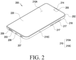
- FIG. 2 is a front perspective view illustrating an electronic device according to an embodiment of the disclosure.
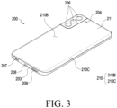
- FIG. 3 is a rear perspective view illustrating an electronic device according to an embodiment of the disclosure.
- the electronic device 200 includes camera modules 205, 206.
- the camera modules 205, 206 are disposed proximate to the front and rear surfaces of the electronic device 200, respectively.
- Camera module 205 can be considered a "selfie camera”.
- an electronic device 200 may include a housing 210 with a front surface 210A, a rear surface 210B, and a side surface 210C surrounding a space between the front surface 210A and the rear surface 210B
- the housing 210 may denote a structure forming part of the front surface 210A, the rear surface 210B, and the side surface 210C of FIG. 2 .
- the housing 210 may include a front plate 202 and a rear plate 211. At least part of the front surface 210A may have a substantially transparent front plate 202 (e.g., a glass plate or polymer plate including various coat layers).
- the rear surface 210B may be formed by a rear plate 211.
- the rear plate 211 may be formed of, e.g., glass, ceramic, polymer, metal (e.g., titanium (Ti), stainless steel (STS), aluminum (Al), or magnesium (Mg)), or a combination of at least two thereof.
- the side surface 210C may be formed by a side bezel structure (or a "side member") 218 that couples to the front plate 202 and the rear plate 211 and includes a metal and/or polymer.
- the rear plate 211 and the side bezel plate 218 may be integrally formed together and include the same material (e.g., glass, metal, such as aluminum, or ceramic).
- the front surface 210A and/or the front plate 202 may be interpreted as a part of the display 220.
- the electronic device 200 may include at least one of a display 220, audio modules 203, 207, and 214 (e.g., the audio module 170 of FIG. 1 ), a sensor module (e.g., the sensor module 176of FIG. 1 ), camera modules 205 and 206 (e.g., the camera module 180 of FIG. 1 ), a key input device 217 (e.g., the input module 150 of FIG. 1 ), and connector holes 208 and 209 (e.g., the connection terminal 178 of FIG. 1 ).
- the electronic device 200 may exclude at least one (e.g., the connector hole 209) of the components or may add other components.
- the display 220 may be visually revealed through, e.g., a majority portion of the front plate 202.
- the surface (or the front plate 202) of the housing 210 may include a screen display area formed as the display 220 is visually exposed.
- the screen display area may include the front surface 210A.
- the electronic device 200 may include a recess or opening formed in a portion of the screen display area (e.g., the front surface 210A) of the display 220 and may include at least one or more of an audio module 214, a sensor module (not shown), a light emitting device (not shown), and a camera module 205 aligned with the recess or opening.
- at least one or more of the audio module 214, sensor module (not shown), camera module 205, fingerprint sensor (not shown), and light emitting device (not shown) may be included on the rear surface of the screen display area of the display 220.
- the display 220 may be coupled with or disposed adjacent to a touch detection circuit, a pressure sensor capable of measuring the strength (pressure) of touches, and/or a digitizer for detecting a magnetic field-type stylus pen.
- the audio modules 203, 207, and 214 may include, e.g., a microphone hole 203 and speaker holes 207 and 214.
- the microphone hole 203 may have a microphone inside to obtain external sounds. According to an embodiment, there may be a plurality of microphones to be able to detect the direction of a sound.
- the speaker holes 207 and 214 may include an external speaker hole 207 and a phone receiver hole 214. According to an embodiment, the speaker holes 207 and 214 and the microphone hole 203 may be implemented as a single hole, or speakers may be included without the speaker holes 207 and 214 (e.g., piezo speakers).
- the sensor modules may generate an electrical signal or data value corresponding to an internal operating state or external environmental state of the electronic device 200.
- the sensor module (not shown) may include, e.g., a first sensor module (not shown) (e.g., a proximity sensor) and/or a second sensor module (not shown) (e.g., a fingerprint sensor) disposed on the front surface 210A of the housing 210.
- the sensor module (not shown) may include a third sensor module (not shown) (e.g., an HRM sensor) and/or a fourth sensor module (not shown) (e.g., a fingerprint sensor) disposed on the rear surface 210B of the housing 210).
- the camera modules 205 and 206 may include a front camera module 205 disposed on the first surface 210A of the electronic device 200 and a rear camera module 206 and/or a flash 204 disposed on the rear surface 210B.
- the camera modules 205 and 206 may include one or more lenses, an image sensor, and/or an image signal processor.
- the flash 204 may include, e.g., a light emitting diode (LED) or a xenon lamp.
- two or more lenses an infrared (IR) camera, a wide-angle lens, and a telephoto lens
- image sensors may be disposed on one surface of the electronic device 200.
- the key input device 217 may be disposed on the side surface 210C of the housing 210.
- the electronic device 200 may exclude all or some of the above-mentioned key input devices 217 and the excluded key input devices 217 may be implemented in other forms, e.g., as soft keys, on the display 220.
- at least a portion of the key input device 217 may be disposed on the side bezel structure 218.
- the light emitting device may be disposed on, e.g., the front surface 210A of the housing 210.
- the light emitting device (not shown) may provide, e.g., information about the state of the electronic device 200 in the form of light.
- the light emitting device (not shown) may provide a light source that interacts with, e.g., the front camera module 205.
- the light emitting device (not shown) may include, e.g., a light emitting diode (LED), an infrared (IR) LED, and/or a xenon lamp.
- the connector holes 208 and 209 may include a first connector hole 208 for receiving a connector (e.g., an earphone jack) for transmitting/receiving audio signals to/from an external electronic device or a connector (e.g., a USB connector) for transmitting/receiving power and/or data to/from the external electronic device and/or a second connector hole 209 for receiving a storage device (e.g., a subscriber identification module (SIM) card).
- SIM subscriber identification module
- the first connector hole 208 and/or the second connector hole 209 may be omitted.
- FIG. 4 is an exploded perspective view illustrating an electronic device according to an embodiment of the disclosure.
- an electronic device 200 may include at least one of a front plate 222 (e.g., the front plate 202 of FIG. 2 ), a display 220. (e.g., the display 220 of FIG. 2 ), a bracket 232 (e.g., a front supporting member), a printed circuit board 240, a battery 250, a rear case 260 (e.g., a rear supporting member), an antenna 270, and a rear plate 280 (e.g., the rear plate 211 of FIG. 3 ).
- a front plate 222 e.g., the front plate 202 of FIG. 2
- a display 220 e.g., the display 220 of FIG. 2
- a bracket 232 e.g., a front supporting member
- a printed circuit board 240 e.g., a printed circuit board
- battery 250 e.g., a battery 250
- a rear case 260 e.g., a rear supporting member
- an antenna 270
- the electronic device 200 may omit at least one (e.g., the rear case 260) of the components or may add other components. At least one of the components of the electronic device 200 may be the same or similar to at least one of the components of the electronic device 200 of FIG. 2 or 3 and no duplicate description is made below.
- the configuration of the side bezel structure 231, the bracket 232, the rear case 260, and/or the rear plate 280 may be interpreted as a structure included in the housing (e.g., the housing 210 of FIG. 2 ) of the electronic device 200.
- the side bezel structure 231, the bracket 232, the rear case 260, and/or the rear plate 280 may be part of the housing 210.
- the bracket 232 may be disposed inside the electronic device 200 to be connected with the side bezel structure 231 or integrated with the side bezel structure 231.
- the bracket 232 may be formed of, e.g., a metal and/or non-metallic material (e.g., polymer).
- the bracket 232 may receive the display 220 on one surface and the printed circuit board 240 on the other surface.
- a processor e.g., the processor 120 of FIG. 1
- a memory e.g., the memory 130 of FIG. 1
- an interface e.g., the interface 177 of FIG. 1
- the battery 250 may be a device for supplying power to at least one component (e.g., the camera module212) of the electronic device 200.
- the battery 250 may include, e.g., a primary cell which is not rechargeable, a secondary cell which is rechargeable, or a fuel cell. At least a portion of the battery 250 may be disposed on substantially the same plane as the printed circuit board 240.
- the battery 250 may be integrally or detachably disposed inside the electronic device 200.
- the rear case 260 may be disposed between the printed circuit board 240 and the antenna 270.
- the rear case 260 may include one surface to which at least one of the printed circuit board 240 and the battery 250 is coupled, and another surface to which the antenna 270 is coupled.
- the antenna 270 may be disposed between the rear plate 280 and the battery 250.
- the antenna 270 may include, e.g., a near-field communication (NFC) antenna, a wireless charging antenna, and/or a magnetic secure transmission (MST) antenna.
- the antenna 270 may perform short-range communication with, e.g., an external device or may wirelessly transmit or receive power necessary for charging.
- the antenna 270 may include a coil for wireless charging.
- an antenna structure may be formed by a portion or combination of the side bezel structure 231 and/or the bracket 232.
- the electronic device 200 may include a camera module 212 disposed in the second housing (e.g., the housing 210 of FIG. 2 ).
- the camera module 212 may be disposed on the bracket 232 and may be a rear camera module (e.g., the camera module 206 of FIG. 3 ) capable of obtaining an image of a subject positioned behind (e.g., the -Z direction) of the electronic device 200.
- at least a portion of the camera module 212 may be exposed to the outside of the electronic device 200 through the opening 282 formed in the rear plate 280.
- the configuration of the camera module 212 may be identical in whole or part to the configuration of the camera module 206 of FIG. 3 .
- the electronic device 200 disclosed in FIGS. 2 to 4 has a bar-type or plate-type appearance but the disclosure is not limited thereto.
- the illustrated electronic device may be a rollable electronic device or a foldable electronic device.
- Rollable electronic device may mean an electronic device at least a portion of which may be wound or rolled or received in a housing (e.g., the housing 210 of FIG. 2 ) as the display (e.g., the display 220 of FIG. 4 ) may be bent and deformed. As the display is stretched out or is exposed to the outside in a larger area according to the user's need, the rollable electronic device may use an expanded second display area.
- FIG. 5 is a rear view illustrating an electronic device according to an embodiment of the disclosure.
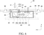
- FIG. 6 is a cross-sectional view taken along line A-A' of FIG. 5 .
- FIG. 7 is an example view illustrating an optical path of a camera module according to an embodiment of the disclosure.
- an electronic device 400 may include a rear plate 380 and a camera module 500.
- the configuration of the rear plate 380 and the camera module 500 of FIG. 5 , 6 , and/or 7 may be identical in whole or part to the configuration of the rear plate 280 and the camera module 212 of FIG. 4 .
- the electronic device 400 may include a camera cover plate 385 disposed on a surface (e.g., the rear surface 210B of FIG. 3 ).
- the camera cover plate 385 may be a portion of the rear plate 380.
- the camera cover plate 385 may be coupled to the rear plate 380 through an ornamental member 389, and when it is viewed from the outside, the ornamental member 389 may be exposed in a form surrounding the camera cover plate 385.
- the camera cover plate 385 may include a plurality of transparent areas 387.
- the electronic device 400 may receive external light or externally radiate light through at least one of the transparent areas 387.
- the electronic device 400 may include at least one camera module 500 (e.g., the camera modules 180 and 212 of FIG. 1 and/or 4) disposed to correspond to at least some of the transparent areas 387 and at least one light source (e.g., an infrared light source) disposed to correspond to others of the transparent areas 387.
- the light source may emit light to the area outside of the electronic device 400.
- the surrounding environment may then reflect the light to provide a better photograph.
- the camera module 500 may receive external light from the outside of the electronic device 400 through any one of the transparent areas 387.
- the electronic device 400 or the camera module 500 may further include a camera supporting member 381.
- the camera supporting member 381 may place or fix at least one of the camera module 500 or another camera module (e.g., a wide-angle camera, an ultra-wide-angle camera, or a macro camera) adjacent to the camera module 500 to the inside of the rear plate 380 or the camera cover plate 385.
- the camera cover plate 385 may visually expose at least a portion of the camera module 500 from an exterior of the electronic device 400 while harmonizing the at least a portion of the camera module 500 with the exterior of the electronic device 400.
- the camera supporting member 381 may be substantially part of the bracket 232 or rear case 260 of FIG. 4 .
- the electronic device 400 may include the camera module 500 or at least one of a wide-angle camera, an ultra-wide-angle camera, a macro camera, a telephoto camera, or an infrared photodiode as a light receiving element.
- the electronic device 400 may include a light source or a flash (e.g., the flash 204 of FIG. 3 ) or an infrared laser diode as a light emitting element.
- the electronic device 400 may emit infrared laser to the subject and receive the infrared laser reflected by the subject, using the infrared laser diode and infrared photo diode, thereby detecting the distance or depth to the subject.
- the electronic device 400 may capture the subject using any one or a combination of two or more of the cameras and, as necessary, provide light to the subject using the flash.
- the wide-angle camera, the ultra-wide-angle camera, or a macro camera may have a shorter length in the optical axis direction of the lens(es) as compared to the telephoto camera (e.g., the camera module 500).
- a telephoto camera e.g., the camera module 500
- the 'overall lens length' may mean the distance from the object-side surface of the first object-side lens to the image plane of the image sensor 411.
- the object side is considered the side of the object that is being photographed while the image plane, or image side, is the side that receives the light.
- the ultra-wide-angle camera, or the macro camera although the lens(es) are arranged along the direction of the thickness (e.g., the thickness measured in the Z-axis direction of FIG. 4 or 6 ) of the electronic device 400, the substantial influence on the thickness of the electronic device 400 may be small.
- the wide-angle camera, the ultra-wide-angle camera, or the macro camera may be disposed such that the direction in which light is incident from the outside to the electronic device 400 and the optical axis direction of the lens(es) are substantially the same.
- the camera module 500 (e.g., a telephoto camera) has a small angle of view but may be useful for capturing a subject at a greater distance and may include more lenses 421a, 421b, 423a, 423b, and 423c.
- the camera module 500 may protrude to the outside of the electronic device 400.
- the camera module 500 may include at least one refractive member 413 and 415 that reflects or refracts the incident light IL in a different direction.
- the light beams IL, RL1 and RL2 may travel substantially along the optical axis O.
- the optical axis O may be defined by lens groups 421 and 423 and/or the refractive members 413 and 415.
- the optical axis O may be a straight line connecting the centers of surfaces of the lens groups 421 and 423 and the refractive members 413 and 415.
- the lens(es) 423a, 423b, and 423c may be disposed to move forward and backward in the incident direction of light or in the traveling direction of reflected or refracted light, preventing an increase in the thickness of the electronic device 400.
- a folded camera (e.g., the camera module 500) may include a first refractive member 413, a second refractive member 415, an image sensor 411, and/or at least one optical member.
- the at least one optical member may be referred to as at least one of a first lens group 421 including first lenses 421a and 421b or a second lens group 423.
- the second lens group 423 may include second lenses 423a, 423b, and 423c and/or a dummy member 423d.
- At least one optical member may guide or focus the light RL1 to the second refractive member 415.
- the at least one optical member may reduce direct incidence of the light RL1 reflected or refracted to the image sensor 411.
- the term “optical member” may mean a component capable of transmitting, refracting, scattering, absorbing or reflecting light.
- “optical member” will be used as meaning the second lenses 423a, 423b, and 423c or the dummy member 423d disposed between the first refractive member 413 and the second refractive member 415, but it should be noted that the term or expression does not limit the embodiments of the disclosure.
- the first refractive member 413, the second refractive member 415, and/or the first lenses 421a and 421b (or the first lens group 421) are a kind of the optical member.
- the optical member disposed between the first refractive member 413 and the second refractive member 415 may be described separately as second lens(es) and/or dummy member and described or a combination of the second lenses 423a, 423b, and 423c or the dummy member 423d may be described as the second lens group 423.
- the first refractive member 413 may include, e.g., a prism or a mirror and reflect or refract he light IL, incident in the first direction D1, in a second direction D2 crossing the first direction D1.
- the first direction D1 may mean a direction in which light IL is incident from the outside to the electronic device 400 or camera module 500 through any one of the transparent areas 387, e.g., when capturing the subject.
- the first direction D1 may mean the direction of capture, the direction toward the subject, the oriented direction of the camera module 500, or a direction parallel thereto.
- the first direction D1 may be parallel to the thickness direction or the Z-axis direction of the electronic device 400.
- the direction (e.g., the second direction D2) of reflection or refraction of light when the direction (e.g., the second direction D2) of reflection or refraction of light is perpendicular to the direction of incidence of light (e.g., the first direction D1), it may be easy to design the camera module 500 or the optical path.
- the second direction D2 may be parallel to the length direction (e.g., the Y-axis direction) or the width direction (e.g., the X-axis direction) of the electronic device 400.
- the structure of the camera module 500 of the disclosure is not limited thereto and may be changed depending on the arrangement and specifications of the camera module 500 or the first refractive member 413 in the electronic device 400.
- the second refractive member 415 may include, e.g., a prism or a mirror and reflect or refract the light RL1, which is reflected or refracted by the first refractive member 413 and incident along the second direction D2, in a third direction D3 crossing the second direction D2.
- the third direction D3 may be substantially perpendicular to the second direction D2.
- the third direction D3 may mean a direction parallel to the Z-axis direction.
- the structure of the camera module 500 of the disclosure is not limited thereto and may be changed depending on the arrangement and specifications of the camera module 500 or the second refractive member 415 in the electronic device 400.
- the third direction D3 may be substantially parallel to the first direction D1.
- the image sensor 411 may be configured to detect the light RL2 which is reflected or refracted by the second refractive member 415 and incident along the third direction D3.
- the light IL incident from the outside may be detected by the image sensor 411 through the first refractive member 413 and the second refractive member 415.
- the electronic device 400 or the camera module 500 may obtain a subject image based on the signal or information detected through the image sensor 411.
- the image sensor 411 may be disposed substantially parallel to the X-Y plane.
- the image sensor 411 may horizontally move on a plane perpendicular to the first direction D1 or the third direction D3.
- the image sensor 411 may be positioned behind the refractive member 415.
- the image sensor 411 may face the exit surface of the refractive member 415.
- the image sensor 411 when the electronic device 400 and/or the camera module 500 performs an image stabilization operation, the image sensor 411 may be shifted in the length direction (e.g., Y-axis direction) or the width direction (e.g., X-axis direction) of the electronic device 400.
- the image sensor 411 is disposed on a plane perpendicular to the first direction D1 or the third direction D3, it is possible to easily increase the size of the image sensor 411 and/or easily secure a space for image stabilization operation in the electronic device having a small thickness (e.g., a thickness of about 10 mm or less).
- the camera module 500 when the camera module 500 is used as a telephoto camera, the quality of the captured image may be further enhanced by including an image stabilization function.
- the performance of the camera module 500 may further increase.
- the camera module 500 may include a lens group (e.g., the first lens group 421 including at least one first lens 421a and 421b) to guide or focus the light IL incident from the first direction D1 to the first refractive member 413.
- the at least one optical member may be disposed between the first refractive member 413 and the second refractive member 415, forming a second lens group 423.
- the first lens e.g., the first lens 421a
- the camera module 500 may have a positive refractive power.
- the optical system from the first lens 421a to the image sensor 411 may be downsized.
- the first lens group 421 may further include an additional first lens(es) 421b to focus or align the light incident from the outside.
- the at least one optical member may include a dummy member 423d and a light blocking means 425.
- the dummy member 423d may be disposed in, e.g., the camera module 500 or the electronic device 400 and may have a cylindrical shape extending along the second direction D2 and transmit the light RL1 traveling along the second direction D2.
- the dummy member 423d may be one of lenses having positive or negative refractive power.
- the dummy member 423d may be a component formed integrally with any one of the second lenses 423a, 423b, and 423c or the second refractive member 415.
- the light blocking member 425 may absorb, scatter, or reflect light. According to an embodiment, the light blocking member 425 may be formed by etching or black-lacquering, and/or printing or depositing a reflective layer on, at least a portion of the outer circumferential surface of the dummy member 423d. According to an embodiment, the light blocking member 425 may be formed or disposed on at least a portion of the outer circumferential surface of the dummy member 423d.
- the refractive members 413 and 415 may include light blocking coating (or immersed paint), when including light blocking coating the refractive members 413 and 415 may be configured to meet Equation 7 below. 0.6 ⁇ Ria Rib ⁇ 1.3
- Ria may denote the refractive index of the raw material of the light blocking coating (e.g., the light blocking member 425) (or immersed paint).
- Ria may denote the refractive index of the raw material except for carbon of the paint of the light blocking coating (or immersed paint).
- Rib may denote the refractive index of the raw material of the refractive members 413 and 415.
- Rib may denote the refractive index of the raw material of the prism forming the effective area 610 of the refractive member (e.g., the refractive member 600 of FIGs. 8a or 8b ).
- a portion of the light reflected or refracted by the first refractive member 413 may be absorbed, scattered, or reflected by the light blocking member 425.
- the light blocking member 425 may substantially block unintentional light incident to the image sensor 411.
- the position of the light blocking member 425 is not limited to the outer circumferential surface of the dummy member 423d.
- the light blocking member 425 may be disposed on at least a portion of the first refractive member 413 and/or at least a portion of the second refractive member 415.
- the light blocking member 425 may be positioned in the dummy area (e.g., the dummy area 620 of FIGs. 8a or 8b ) of the refractive members 413 and 415.
- light may be incident to the camera module 500 from a direction other than the direction of capture or oriented direction, or may travel in a path other than the optical path (e.g., the path indicated by 'RL1' and/or 'RL2' in FIG. 7 ) during reflection or refraction in the camera module 500 and be detected by the image sensor.
- the light incident on the image sensor through an unintended path or an image generated thereby may be denoted as 'ghost light' or 'ghost image.”
- a ghost image can appear as a faint duplicated of a photographed object that is slightly offset from the photographed object in the image. The ghost image may deteriorate the quality of the image obtained through the camera module 500.
- the light blocking member 425 may absorb, scatter, or reflect ghost light (e.g., light reflected or refracted by the first refractive member 413), blocking direct incidence of the ghost light to the image sensor 411.
- ghost light e.g., light reflected or refracted by the first refractive member 413
- the light which sequentially passes in the first direction D1, second direction D2, and/or third direction D3 from the camera module 500 e.g., the light along the path indicated by 'IL,' 'RL1,' and 'RL2' of FIG. 7
- the image sensor 411 may absorb, scatter, or reflect ghost light (e.g., light reflected or refracted by the first refractive member 413), blocking direct incidence of the ghost light to the image sensor 411.
- the light which sequentially passes in the first direction D1, second direction D2, and/or third direction D3 from the camera module 500 e.g., the light along the path indicated by 'IL,' 'RL1,' and 'RL2' of FIG.
- the at least one optical member may include at least one second lens 423a, 423b, and 423c that moves back and forth along substantially the same axis as the second direction D2 between the first refractive member 413 and the second refractive member 415.
- the electronic device 400 or the camera module 500 may adjust the focal length by moving back and forth at least one second lens 423a, 423b, and 423c with respect to substantially the same axis as the second direction D2.
- a small electronic device such as a smartphone, may have a thickness of about 10 mm or less and, in this case, the range in which the lens may advance and retreat in the thickness direction may be limited.
- the second direction D2 may be substantially parallel to the length direction (e.g., the Y-axis direction of FIG. 4 ), the width direction (e.g., the X-axis direction of FIG. 4 ) and/or the X-Y plane.
- the range in which the at least one second lens 423a, 423b, and 423c may move back and forth may be large.
- the at least one second lens 423a, 423b, and 423c moves back and forth along substantially the same axis as the second direction D2, it is possible to enhance the degree of design freedom in securing a forward/backward movement space for focus adjustment (or focal length adjustment) while enhancing the telephoto performance of the camera module 500.
- the electronic device 400 and/or the camera module 500 may further include an infrared cut filter 419.
- the infrared cut filter 419 may block light in an infrared or near infrared wavelength band from being incident to the image sensor 411 and may be disposed in any position in the light path between the first lens 421a and the image sensor 411.
- the infrared cut filter 419 may be disposed in a position close to the image sensor 411 (e.g., between the image sensor 411 and the second refractive member 415), preventing or suppressing the infrared cut filter 419 from being visually exposed to the outside.
- the first refractive member 413, the second refractive member 415, and/or at least one optical member may include an infrared cut coating layer.
- the infrared cut filter 419 may be omitted.
- the infrared cut coating layer may be provided on at least one of the image sensor-side surface and the object-side surface of the dummy member 423d or the second refractive member 415. Accordingly, the image sensor 411 may detect light substantially transmitted through the infrared cut filter 419 (or the infrared cut coating layer).
- the electronic device 400 and/or the camera module 500 may not include an optical member, e.g., the dummy member 423d.
- the light blocking member 425 may be disposed on at least a portion of the infrared cut filter 419.
- FIGS. 6 and 7 illustrate a structure in which the electronic device 400 and/or the camera module 500 includes two refractive members 413 and 415
- the structure of the electronic device 400 and/or the camera module 500 is not limited thereto.
- the electronic device 400 may include the first refractive member 413 but may not include the second refractive member 415.
- the image sensor 411 and/or the infrared cut filter 419 may be positioned substantially parallel to the second lens group 423.
- the refractive members 413 and 415 of the disclosure may be selectively designed depending on the structure of the camera module 500.
- the refractive member e.g., the refractive member 415 of FIG. 6
- the refractive member e.g., the refractive member 415 of FIG. 7
- the shapes of the refractive members 413 and 415 are not limited to the structures shown in the disclosure.
- the refractive members 413 and 415 may have a structure (e.g., a column structure having a diamond-shaped bottom) other than a triangular or trapezoidal prism.
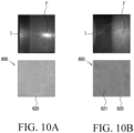
- FIG. 8a is a perspective view illustrating a refractive member according to an embodiment of the disclosure.
- FIG. 8b is a perspective view illustrating a refractive member according to an embodiment of the disclosure.
- FIG. 9 is a side view illustrating a refractive member according to an embodiment of the disclosure.
- the refractive member 600 may include an effective area 610 and a dummy area 620.
- the term 'effective area 610' may refer to a portion that refracts light toward the image sensor 411.
- the effective area 610 may refer to a progress path of light to be incident on the image sensor 411 or a portion through which light passes.
- light including image information of a subject may be guided to the image sensor 411 via at least a portion of the effective area 610.
- a portion of the effective area 610 (e.g., the second surface 600b) may substantially reflect light to be incident on the image sensor 411.
- the dummy area 620 may be a part of the refractive member 600 and a part through which light guided to the image sensor 411 does not pass.
- the dummy area 620 may be one of the structures that cause internal reflection to be described later.
- the dummy area 620 may be provided on at least a portion of the edge of the effective region 610.
- the term 'edge of the effective area 610' may refer to a side of the first surface 600a to be described later in contact with the side portion 601, a side of the second surface 600b to be described later in contact with the side portion 601, and/or a side of the third surface 600c to be described later in contact with the side portion 601.
- the dummy area 620 is substantially disposed on the side portion 601.
- the term 'edge of the effective area 610' may refer to at least a part of the first surface 600a to be described later in contact with the side portion 601, at least a part of the second surface 600b to be described later in contact with the side portion 601, and/or at least a part of the third surface 600c to be described in contact with the side portion 601.
- the dummy area 620 is disposed on the side portion 601 and is disposed on a portion P11, P12, P21, P22, P31, and P32 of the first surface 600a, the second surface 600b, and/or the third surface 600c.
- the dummy area 620 may scatter or absorb at least a portion of light incident to the dummy area 620 by satisfying conditions for a bidirectional scattering distribution function to be described later.
- 'scattering or absorbing at least a part of incident light' may be understood as suppressing light incident to the image sensor 411 through an undesigned path by suppressing internal reflection in the dummy area 620.
- the dummy area 620 includes a roughening pattern 621 and/or a nanostructure, at least a portion of the incident light may be scattered.
- a light blocking member e.g., the light blocking member 425 in FIG.
- the light blocking member e.g., the light blocking member 425 in FIG. 6
- the light-shielding member or light-blocking coating that absorbs light may be replaced with a paint immersed in the dummy area 620 or may be disposed together with the paint immersed in the dummy area 620. In one embodiment, when the light blocking member or the light blocking coating is combined with a paint immersed in the dummy area 620, the absorption rate of incident light may be improved.
- the dummy area 620 may be disposed on at least a portion of the edge of the effective region 610.
- the dummy area 620 may be disposed on at least both sides of the refractive member 600 (e.g., the side portion 601 of FIG. 8A or 8B ; the first side portion 601a and/or the second side portion 601b).
- the configuration of the refractive member 600 of FIGS. 8a, 8b and 9 may be identical in whole or part to the configuration of the first protection member 413 and/or the second protection member 415 of FIGS. 6 and 7 .
- the refractive member 600 may reflect or refract at least a portion of the light passing through the optical member (e.g., the first lens group 421 and/or the second lens group 423 of FIG. 6 ).
- the effective area 610 may transmit at least a portion of light or refract at least a portion of light.
- the effective area 610 may provide a path through which at least a portion of the light transferred from the lens (e.g., the first lens group 421 and/or the second lens group 423 of FIG. 6 ) passes.
- the effective area 610 may be formed of a substantially transparent material.
- the effective area 610 may be referred to as an area where a roughening pattern 621 is not formed in the refractive member 600.
- the effective area 610 may provide a path through which light (e.g., light IL of FIG. 7 ) substantially passes.
- the effective area 610 may be a portion of the refractive member 600 through which the optical axis (e.g., the optical axis O of FIG. 7 ) passes.
- the effective area 610 may be positioned in at least a portion of the center portion of the refractive member 600.
- the light e.g., light IL of FIG. 7
- the camera module 500 may be substantially transferred to the effective area 610.
- the effective area 610 may be a portion of the refractive member 600 for adjusting the path of light.
- the effective area 610 may include surfaces for adjusting the path of light.
- the effective area 610 may include an incident surface to which light is first transferred among surfaces of the refractive member 600.
- the incident surface may be referred to as an initial incident surface or a first incident surface.
- the effective area 610 may include a reflective surface inclined with respect to the first incident surface of the refractive member 600.
- the reflective surface may not form a right angle with the incident surface.
- the reflective surface may reflect at least a portion of the light passing through to the incident surface.
- a plurality of reflective surfaces may be provided on the refractive member 600.
- the effective area 610 may include at least one reflective surface.
- the effective area 610 may include an exit surface through which light is emitted last among the surfaces of the refractive member 600.
- the exit surface may be referred to as a final exit surface or a first exit surface.
- the first surface 600a may be denoted as an incident surface, the second surface 600b as a reflective surface, and the third surface 600c as an exit surface.
- the first surface 600a may be disposed to face the subject and may be disposed to cross or substantially perpendicular to light incident from the outside.
- the third surface 600c may be disposed to cross or substantially perpendicular to light emitted toward the image sensor 411.
- a plurality of second surfaces 600b functioning as reflective surfaces may be provided, and may be guided to the third surface 600c by reflecting or refracting light incident through the first surface 600a.
- the refractive member 600 may have various shapes (e.g., a triangular prism, a trapezoidal prism, or a rhombic prism). What has been described about the incident surface, the reflective surface, and/or the exit surface may be applied to the refractive member 600 having various shapes.
- the incident surface, the reflective surface, or the exit surface will be understood by one of ordinary skill in the art. For example, reflection also occurs on the incident surface where light is incident, but one of ordinary skill in the art may distinguish the incident surface from the reflective surface considering the amount of reflection and incidence of light.
- the refractive member 600 may include a component for enhancing light transmission and/or light refraction in the effective area 610.
- a component for enhancing light transmission and/or light refraction in the effective area 610 For example, at least one of a low-reflective coating layer or a mirror coating layer may be disposed on the effective area 610.
- materials of the low-reflective coating layer and the mirror coating may be different from that of the refractive member 600.
- the refractive member 600 may reflect or refract light 1 to 5 times. The number of times the refractive member 600 reflects or refracts light may be changed based on the shape of the refractive member 600.
- the dummy area 620 may reduce light reflection.
- the term 'dummy area 620 reduces the reflection of light' may be understood as suppressing progress toward the image sensor 411 by scattering or absorbing light incident on the dummy area 620.
- the dummy area 620 may include a roughening pattern 621. Due to be provided with the roughening pattern 621, the reflectance of the dummy area 620 may be lower than the reflectance of the effective region 610, or at least a portion of the light incident on the dummy area 620 may be scattered.
- the roughening pattern 621 may scatter at least a portion of light incident on the dummy area 620 or may at least suppress progress to an image sensor (e.g., the image sensor 411 of FIG. 7 ).
- the roughening pattern 621 may refer to a plurality of depressions or protrusions formed in the refractive member 600. According to an embodiment, the roughening pattern 621 may be referred to as a corroded area or corroded surface. According to an embodiment, the roughening pattern 621 may be referred to as an irregularity pattern including a plurality of depressions and/or a plurality of protrusions. According to an embodiment, the dummy area 620 may be a portion of the refractive member 600 required for shaping the refractive member and/or coupling with another component of the electronic device (e.g., the electronic device 200 of FIG. 2 ) or fixing the position of the refractive member 600.
- another component of the electronic device e.g., the electronic device 200 of FIG. 2
- the dummy area 620 may be partially disposed on the first surface 600a, the second surface 600b, and/or the third surface 600c.
- the dummy area 620 may be partially disposed on the side end of the effective region 610 on the first surface 600a, the second surface 600b, and/or the third surface 600c.
- the dummy area 620 may be referred to as an ineffective area.
- the roughening pattern 621 may be referred to as a fine pattern.
- the roughening pattern 621 may be formed by corrosion or etching (e.g., dry etching).
- a nanostructure replacing the roughening pattern 621 since a nanostructure replacing the roughening pattern 621 is provided, light incident on the dummy area 620 may be absorbed or scattered.
- a roughening pattern 621 and a nanostructure are combined in the dummy area 620 to scatter light incident on the dummy area 620, thereby further suppressing progress toward the image sensor 411.
- the degree of reflection of the light incident on the dummy area 620 may be reduced due to the roughening pattern 621 and/or nanostructure, thereby reducing flare in the image obtained from the camera module (e.g., the camera module 500 of FIG. 6 ).
- the camera module e.g., the camera module 500 of FIG. 6
- unintended reflected light rays or unintended refracted light rays
- the depth or etching amount of the roughening pattern 621 may be about 1 ⁇ m.
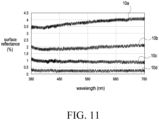
- the roughness average (Ra) of the dummy area 620 may be about 1.0 ⁇ m or more.
- the term 'roughness average (Ra)' may be, for example, a reference to the average roughness of the center line of the surface of an object or structure.
- the dummy area 620 may form at least a portion of an outer surface of the refractive member 600.
- the dummy area 620 may be positioned on at least a portion of the side portion 601 or the edge of the refractive member 600 (e.g., edge(s) of the first surface 600a, the second surface 600b, and/or the third surface 600c).
- the dummy area 620 may surround at least a portion of the effective area 610.
- the side portion 601 may be referred to as a portion of the refractive member 600 through which the optical axis (e.g., the optical axis O in FIG. 7 ) does not pass.
- light to be guided to the image sensor 411 may progress, inside the refractive member 600, a region (e.g., the effective area 610) between both edges of the refractive member 600 and may not pass through the dummy area 620.
- the dummy area 620 may be substantially parallel to the optical axis O.
- the arrangement of the dummy area 620 with respect to the optical axis O may be variously changed. In the arrangement of the dummy area 620, specifications required by the electronic device 400 or the camera module 500 of FIG. 6 may be considered without interfering with the progress path of light to be guided to the image sensor 411.
- the optical properties or optical characteristics of the dummy area 620 may be different from those of the effective area 610 due to the roughening pattern 621 and/or nanostructure.
- the first surface roughness of the dummy area 620 may be larger than the second surface roughness of the effective area 610.
- the first surface reflectance of the dummy area 620 may be lower than the second surface reflectance of the effective area 610.
- the first surface reflectance of the dummy area 620 may be about 2.0% or less.
- the first surface reflectance of the dummy area 620 may be about 0.5% or less.
- the second surface reflectance of the effective area 610 may exceed about 2.0%.
- the dummy area 620 may be a path through which the optical axis O does substantially not pass.
- the dummy area 620 may be at least partially disposed on at least a portion of the side surface (e.g., the side portion 601) of the refractive member 600.
- the refractive member 600 may have substantially a triangular pillar shape or a triangular pyramid shape.
- the refractive member 600 may include a first surface 600a facing outward of the electronic device (e.g., the electronic device 200 of FIG. 2 ), a second surface 600b configured to reflect or refract at least a portion of the light passing through the first surface 600a, and a third surface 600c for transferring at least a portion of the light reflected or refracted by the second surface 600b to the image sensor (e.g., the image sensor 411 of FIG. 7 ).
- the first surface 600a may be substantially perpendicular to the third surface 600c.
- the second surface 600b may extend from the first surface 600a to the third surface 600c.
- the second surface 600b may be inclined with respect to the first surface 600a and the third surface 600c.
- the number of the first surface 600a, the second surface 600b, and/or third surface 600c, or the relative arrangement (e.g., angle to each other) of the first surface 600a, the second surface 600b, and/or third surface 600c is/are not limited to the above-described examples, and may be appropriately changed according to the design specification of the electronic device (e.g., the electronic device 101, 200, 400 of FIGs. 1 through 5 ) and/or the camera module (e.g., camera module 500 of FIG. 6 ).
- the refractive member 600 when the refractive member 600 is in the shape of a parallelogram pillar, a rhombus pillar, or a trapezoidal pillar, multiple surfaces (e.g., the second surface 600b) that reflect or refract light may be provided.
- the effective area 610 may provide a light path (e.g., a path through which light is transmitted or progress).
- the effective area 610 may provide an incident surface, a reflective surface, and an exit surface of the refractive member 600.
- the first surface 600a of the refractive member 600 may be denoted as an incident surface
- at least a portion of the third surface 600c of the refractive member 600 as an exit surface.
- the refractive member 600 may include a side portion 601 positioned defined by the first surface 600a, the second surface 600b, and the third surface 600c.
- the side portion 601 may be substantially an area (or a surface) surrounded by a portion of an edge of the first surface 600a, a portion of an edge of the second surface 600b, and a portion of an edge of the third surface 600c, and may be referred to as a portion of the surface of the refractive member 600.
- the side portion 601 may include a first side surface 601a and a second side surface 601b opposite to the first side surface 601a.
- a portion of the dummy area 620 may be positioned on the side portion 601.
- the dummy area 620 may be at least partially positioned on at least one of the first side surface 601a or the second side surface 601b.
- the degree of transfer of light incident on the side portion 601 from an outside of the refractive member 600 or an inside of the refractive member 600 to the image sensor 411 may be reduced.
- the dummy area 620 and/or the side portion 601 may suppress stray light incident to the image sensor such that the dummy area 620 and/or the side portion 601 substantially absorb or scatter the incident light.
- the refractive member 600 may include a substantially transparent material.
- the refractive member 600 may be formed of glass.
- the roughening pattern 621 may be formed by a laser.
- the roughening pattern 621 may be referred to as a protruding or recessed shape formed on the glass of the refractive member 600.
- the refractive member 600 has been described as having a triangular pillar shape or a triangular pyramid shape, but the shape of the refractive member 600 is not limited thereto.
- the refractive member 600 may have a pillar shape in which the side portion 601 has a square (e.g., trapezoidal or rectangular) shape.
- the refractive member 600 may have a diamond-shaped cross section.
- the refractive member 600 may have a pillar shape in which the side portion 601 has a diamond shape.
- the refractive member 600 may be formed of a resin.
- the refractive member 600 may include plastic that may be manufactured using a mold.
- the roughening pattern 621 may be formed by a mold.
- the roughening pattern 621 may be formed by a mold including protrusions corresponding to the roughening pattern 621.
- the refractive member 600 may include a light blocking coating disposed on the dummy area 620 or a paint immersed into the dummy area 620.
- the configuration of the light blocking coating may be identical in whole or part to the configuration of the light blocking member 425 of FIG. 6 .
- the light blocking coating or the immersed paint may reduce the degree of reflection of the light incident on the dummy area 620.
- the light absorption of the refractive member 600 where the light blocking coating or the immersed paint is positioned may be higher than the light absorption of the area where the light blocking coating or the immersed paint is not present, and the light transmittance of the refractive member 600 where the light blocking coating or the immersed paint is positioned may be lower than the light transmittance of the area where the light blocking coating or the immersed paint is not present.
- the light-blocking coating e.g., black lacquer
- the immersed paint may be positioned in the dummy area 620 where the roughening pattern 621 is formed. Due to the roughening pattern 621, the occurrence of flare may be reduced and, due to the light blocking coating or the immersed paint, light absorption may be increased and light transmittance may be decreased.
- the refractive member 600 may include a chamfered area 630 to reduce breakage of the refractive member 600.
- the chamfered area 630 may be referred to as a portion of a cut edge of the refractive member 600.
- the dummy area 620 may be partially positioned in the chamfered area 630.
- the dummy area 620 may form at least a portion of the chamfered area 630. Since the dummy area 620 is positioned in the chamfered area 630, the degree of reflection of the light incident on the chamfered area 630 may be reduced.
- the dummy area 620 may have a designated bidirectional scattering distribution function (BSDF) to reduce internal reflection.
- BSDF bidirectional scattering distribution function
- internal reflection may be referred to as a phenomenon in which light entering the inside of the camera module (e.g., the camera module 500 of FIG. 6 ) is unintentionally reflected by a component. Due to internal reflection, the quality of the photo captured by the camera module 500 may be reduced, or a stain or flare may occur.
- a phenomenon (e.g., flare) due to internal reflection may reduce as the surface reflectance of the refractive member 600 decreases, and the surface etching amount increases.
- the surface reflectance of the dummy area 620 of the refractive member 600 is about 2.0% or less and the surface etching amount (e.g., the depth of the roughening pattern 621) is about 1 ⁇ m or more, flare may be reduced.
- the surface etching amount of the dummy area 620 e.g., the depth of the roughening pattern 621
- the surface reflectance of the dummy area 620 is controlled to be approximately 2.0% or less (e.g., approximately 0.5%), and the flare of the image obtained through the image sensor 411 may be substantially removed.
- surface reflectance or surface etching are illustrative and may vary depending on design parameters, such as the relative location of the image sensor 411 and refractive member 600, or presence of the light-shielding coating (or the immersed paint). For example, it is noted that the values mentioned regarding the surface reflectance or surface etching amount do not limit the embodiment(s) of the present disclosure.
- the scattering coefficient (BSDF) of the dummy area 620 may be set to meet the following equations.
- the scattering coefficient (BSDF) may be referred to as the sum of the bidirectional reflectance distribution function (BRDF) and the bidirectional transmittance distribution function (BTDF).
- the scattering coefficient may be referred to as a bidirectional scattering distribution function (BSDF).
- the scattering coefficient may be a function for determining how much light is reflected or transmitted when light is incident on an object.
- the bidirectional reflectance distribution function may be a function for determining in which direction light is reflected.
- the bidirectional transmittance distribution function may be a function for determining in which direction light is transmitted.
- the first scattering coefficient of the dummy area 620 may be lower than the second scattering coefficient of the effective area 610.
- the scattering coefficient of the dummy area 620 may meet Equation 1 below.
- the scattering coefficient of the dummy area 620 may be referred to as a bidirectional reflectance distribution function.
- the scattering coefficient can be determined substantially by the bidirectional reflectance distribution function.
- B-B 0 may denote an angular difference in scattered light in a sine direction.
- B may be the angle of the scattered light
- B 0 may be the reference angle.
- the reference angle may be an 0.01 radian (about 0.57 degrees)-inclined angle from the reflective surface.
- Equation 1 which means the scattering coefficient may be interpreted as a modified expression of the Harvey-Shack model.
- Equation 1 which means the scattering coefficient may be interpreted as a modified expression of the Harvey-Shack model.
- b indicating the scattering coefficient value at the reference angle may meet Equation 2 below.
- Equation 3 the unit of S may be degrees. ⁇ 6.0 ⁇ S ⁇ ⁇ 0.05
- Equation 4 the unit of l may be degrees. 0.02 ⁇ l ⁇ 1.9
- b, S, and/or l may be changed according to the design of the camera module 500.
- b may be 0.05 to 0.1.
- S may be -4.2 to -0.05.
- S may be -4.0 to -0.5.
- m indicating cosine power may meet Equation 5 below. 0 ⁇ m ⁇ 1.6
- n which refers to angle power, may meet Equation 6 below. 1.1 ⁇ n ⁇ 9.0
- the cosine power and/or the angle power may be changed according to the design of the camera module 500.
- m may be in a range from about 0.0001 to about 1.0.
- n may be in a range from about 1.15 to about 1.56.
- the structure of the refractive member 600 of FIGS. 8a, 8b and/or 9 may be used together with the structure of the camera module 500 of FIGS. 6 and/or 7.
- FIGS. 10A to 10D are enlarged views of an optical member and views of captured images according to an embodiment of the disclosure.
- FIG. 11 is a graph illustrating surface reflectance of an optical member according to an embodiment(s) of the disclosure.
- the refractive member 600 may include a dummy area 620 where a roughening pattern 621 is positioned.
- the configuration of the dummy area 620 of FIG. 10A, 10B , 10C and/or 10D may be identical in whole or part to the configuration of the dummy area 620 of FIGs. 8a and 8b .
- Fig. 11 the graph indicated by '10a' measures and illustrates the surface reflectance in the dummy area 620 of Fig. 10a
- the graph indicated by '10b' measures and illustrates the surface reflectance in the dummy area 620 of Fig.
- the graph indicated by '10c' measures and illustrates the surface reflectance in the dummy area 620 of Fig. 10c
- the graph indicated by '10d' measures the surface reflectance in the dummy area 620 of Fig. 10d .
- the flare F generated in the image I captured by the camera module may be suppressed based on the roughening pattern 621.
- the refractive member 600 of FIG. 10A illustrates the dummy area 620 that does not include a roughening pattern.
- the refractive member 600 of FIGS. 10B , 10C and 10D illustrates a dummy area 620 that includes a roughening pattern 621.
- the size of the flare F generated in the captured image I in FIG. 10A may be larger than the size of the flare F generated in the captured image I in FIGS. 10B and 10C .
- the size of the flare F may be determined based on the depth of the roughening pattern 621.
- the depth of the roughening pattern 621 may be formed in various ways.
- FIG. 10B includes a roughening pattern 621 having a depth of about 14 ⁇ m.
- FIG. 10C includes a roughening pattern 621 having a depth of about 6 ⁇ m.
- FIG. 10D includes a roughening pattern 621 having a depth of about 52 ⁇ m.
- the roughening pattern 621 of FIG. 10B is formed deeper than the roughening pattern 621 of FIG. 10C , but has a higher surface reflectance.
- the surface reflectance may generally decrease as the depth of the roughening pattern 621 increases.
- the size of the flare F generated in the image I may decrease.
- the size of the flare F of the image I captured by the refractive member 600 of FIG. 10D may be smaller than the size of the flare F of the image I captured by the refractive member 600 of FIG. 10C .
- a roughening pattern 621 having a depth of about 1 ⁇ m or more is provided to the dummy area 620 to suppress a flare phenomenon in the obtained image, and the surface reflectance may be controlled to be about 2% or less by including the roughening pattern 621 in the dummy area 620.
- the surface reflectance of the dummy area 620 may be controlled to be approximately 0.5% or less.
- the flare F may not substantially occur.
- the image I captured by the refractive member 600 of FIG. 10D may have no flare F.
- FIG. 12 is a perspective view illustrating a refractive member according to an embodiment of the disclosure.
- some reference numbers for the configuration of the refractive member are omitted for simplicity of the drawings, and a configuration corresponding to the omitted reference numbers may be described with reference to FIG. 8A or FIG. 8B .
- the refractive member 700 may include a first surface 711 functioning as an incident surface, second surfaces 712a and 712b functioning as reflective surfaces, and a third surface 713 functioning as an exit surface.
- a dummy area 720 may be disposed on at least a portion of the edges of the first surface 711, the second surfaces 712a, 712b, and/or the third surface 713.
- a side portion e.g., the first side surface 601a and the second side surface 601b of FIG. 8A or 8B
- the refractive member 700 may be substantially a part of the dummy area 720.
- the light guided to the image sensor may be emitted through the third surface 713 through a portion of the refractive member 700 (e.g., the effective region 610 of FIG. 8A or 8B ) between the dummy areas 720.
- the dummy area 720 may satisfy the conditions presented through the above-described equations by at least partially including a roughening pattern (e.g., roughening pattern 621 of FIG. 8A or 8B ) and/or a nanostructure.
- a roughening pattern e.g., roughening pattern 621 of FIG. 8A or 8B
- a nanostructure e.g., light incident on the dummy area 720 may be scattered (or absorbed) by a roughening pattern and/or nanostructure.
- the first surface 711 is a surface disposed to face an external space or a lens (e.g., the first lens group 421 or the second lens group 423 of FIG. 7 ) and may function as an incident surface in the refractive member 700.
- light may be incident on the refractive member 700 from the outer space or via the lens(s) through an area illustrated as 'IA' in the first surface 711.
- light incident into the refractive member 700 through the first surface 711 may be sequentially reflected by the second surface indicated by '712a' (hereinafter referred to as '2-1 surface 712a') and the second surface indicated by '712b' (hereinafter referred to as '2-2 surface 712b'), and guided to the third surface 713.
- the third surface 713 is a surface disposed to face the outer space of the refractive member 700 or the image sensor 411 and may function as an exit surface in the refractive member 700.
- light may be emitted from the inside of the refractive member 700 toward the outer space or the image sensor 411 through an area illustrated as 'OA' in the third surface 713.
- light reflected from the 2-1 surface 712a may be additionally reflected inside the refractive member 700 before reaching the 2-2 surface 712b.
- light guided to the image sensor 411 is incident into the refractive member 700 through the incident area IA, and may be sequentially reflected by the 2-1 surface 712a, the first surface 711, the third surface 713 and/or the 2-2 surface 712b in the refractive member 700, and then may be emitted through the emitting area OA.
- Such a guide path or a reflection path may be implemented using an inclination angle (e.g., an angle A between the first surface 711 and the 2-1 surface 712a) formed by the first surface 711, the second surfaces 721b, and/or the third surface 713).
- light incident from the outside of the refractive member 700 or from the inside of the refractive member 700 to the dummy area 720 may cause flare to be generated in the obtained image.
- the light to be focused on the image sensor 411 using the refractive member 700 is guided substantially through the area between the dummy areas 720 (e.g., the effective area 610 of FIG. 8A or 8B ) and the quality of the subject image may be degraded when the light incident to the dummy area 720 reaches the image sensor 411.
- the dummy area 720 may suppress the generation of flares in the obtained image by having a light scattering (or light absorption) tendency such as a roughening pattern (e.g., roughening pattern 621 of FIG. 8A or 8B ) and/or nanostructure.
- a light scattering (or light absorption) tendency such as a roughening pattern (e.g., roughening pattern 621 of FIG. 8A or 8B ) and/or nanostructure.
- the refractive member 700 may be implemented by coupling another refractive member having a polygonal pillar shape to the refractive member 600 of Fig. 8A or 8B .
- the refractive member 700 of the above-described embodiment may be implemented by combining two or more different prisms. At least one of two or more different prisms may include the dummy area of the above-described embodiment.
- the refractive member according to an embodiment of the present disclosure may be implemented by combining two or more prisms, and at least one of the two or more prisms may include a dummy area to scatter or absorb light passing or transmitting through the ineffective region.
- a mobile phone has been described, but the disclosure is not limited thereto.
- the contents of the disclosure may be applied to an electronic device including a refractive member (e.g., the refractive member 600 of FIGs. 8A or 8B ) in a folded zoom structure (e.g., a telephoto camera).
- the electronic device may be a wearable device, a digital camera, or a drone.
- the refractive member 600 of the disclosure may include a roughening pattern 621 formed on a portion where light reflection may occur (e.g., an edge and/or side portion 601 of the refractive member 600). Due to the roughening pattern 621, flare in the image obtained by the refractive member 600 may be mitigated.
- the roughening pattern 621 may be replaced with a nanostructure provided in the dummy region 620.
- the roughening pattern 621 and nanostructure may be combined to satisfy at least one of the conditions presented through the above-described equations, thereby suppressing generation of flares in the obtained image.
- a camera module (e.g., the camera module 500 of FIG. 6 ) may comprise a refractive member (e.g., the first refractive member 413, the second refractive member 415 of FIG. 6 , and/or the refractive member 600 of FIGs. 8A or 8B ) configured to reflect or refract at least a portion of light received by the camera module and an image sensor (e.g., the image sensor 411 of FIG. 6 ) configured to detect at least a portion of light reflected or refracted by the refractive member.
- the refractive member may include an effective area (e.g., the effective area 610 of FIGs.
- the dummy area is configured to scatter at least a part of the light incident into the dummy area by satisfying the following Equation 1, Equation 2, Equation 3, and Equation 4 for a bidirectional scattering distribution function.
- Equation 1, Equation 2, Equation 3, and Equation 4 for a bidirectional scattering distribution function.
- BSDF b 1 + B ⁇ B 0 l ⁇ g n S 2 g m .
- B-B0 may denote an angular difference in scattered light in a sine direction.
- g may denote an average of an angle of scattered light in a cosine direction and an angle of incident light in the cosine direction.
- b may denote a BSDF value at a reference angle, and S may denote an angle of the BSDF.
- l may denote the angle at which a change in reflected light relative to incident light starts.
- m may denote the cosine power.
- n may denote the angle power.
- the dummy area may be set to meet at least one of Equation 5 or Equation 6 below.
- Equation 5 0 ⁇ m ⁇ 1.6.
- Equation 6 1.1 ⁇ n ⁇ 9.0
- the dummy area may include at least one of a nanostructure disposed on a surface of the refractive member or a roughing pattern with a surface roughness of 1.0 ⁇ m or more.
- the refractive member may be an optical lens or a prism including a first surface (e.g., the first surface 600a of FIGs. 8A or 8B ) configured to reflect, refract, or transmit the light and a second surface (e.g., the second surface 600b of FIGs. 8A or 8B ) configured to reflect or refract at least a portion of the light passing through the first surface.
- a first surface e.g., the first surface 600a of FIGs. 8A or 8B
- a second surface e.g., the second surface 600b of FIGs. 8A or 8B
- the refractive member may include a side portion (e.g., the side portion 601 of FIGs. 8A or 8B ) at least partially defined by the first surface and the second surface.
- the side portion may include a first side surface (e.g., the first side surface 601a of FIGs. 8A or 8B ) and a second side surface (e.g., the second side surface 601b of FIGs. 8A or 8B ) opposite to the first side surface.
- at least a portion of the dummy area may be positioned on at least one of the first side surface or the second side surface.
- the refractive member may include a paint immersed into the dummy area or a light blocking coating (e.g., the light blocking member 425 of FIG. 6 ) disposed on the dummy area, and the immersed paint or the light blocking coating is configured to absorb light incident to the dummy area.
- the refractive members 413 and 415 may be set to meet Equation 7 below. [Equation 7] 0.6 ⁇ Ria Rib ⁇ 1.3 .
- Ria may denote the refractive index of the raw material of the immersed paint or the light blocking coating (e.g., the light blocking member 425).
- Rib may denote the refractive index of the raw material of the refractive members 413 and 415.
- the refractive member may include at least one of a mirror coating layer or a low-reflective coating layer disposed on the effective area.
- the refractive member may include a chamfered area (e.g., the chamfered area 630 of FIG. 9 ) positioned at an edge of the refractive member.
- the dummy area may be positioned in the chamfered area.
- the refractive member may include glass and the dummy area includes a roughening pattern.
- the refractive member may include a resin and the dummy area includes a roughening pattern.
- the image sensor may be positioned behind the refractive member.
- the refractive member may be configured to reflect or refract light 1 to 5 times.
- a first scattering coefficient of the dummy area may be lower than a second scattering coefficient of the effective area.
- a first surface reflectance of the dummy area may be lower than a second surface reflectance of the effective area.
- a first surface roughness of the dummy area may be higher than a second surface roughness of the effective area.
- a surface reflectance of the dummy area of the refractive member may be 2.0% or less.
- an electronic device may comprise a housing (e.g., the housing 210 of FIG. 2 ) and a camera module (e.g., the camera module 500 of FIG. 6 ) at least a portion of which is disposed in the housing.
- the camera module may include an optical member (e.g., the first lens group 421 and/or the second lens group 423 of FIG. 6 ) including at least one lens (e.g., the first lens 421a or 421b of FIG. 6 and/or the second lens 423a, 423b, or 423c of FIG.
- the refractive member may include an effective area (e.g., the effective area 610 of FIGs. 8A or 8B ) configured to provide a path of the light and a dummy area (e.g., the dummy area 620 of FIG.
- the dummy area is configured to scatter at least a part of the light incident into the dummy area by satisfying the following Equation 1, Equation 2, Equation 3, and Equation 4 for a bidirectional scattering distribution function.
- Equation 1, Equation 2, Equation 3, and Equation 4 for a bidirectional scattering distribution function.
- B-B0 may denote an angular difference in scattered light in a sine direction.
- g may denote an average of an angle of scattered light in a cosine direction and an angle of incident light in the cosine direction.
- b may denote a BSDF value at a reference angle
- S may denote an angle of the BSDF.
- l may denote the angle at which a change in reflected light relative to incident light starts.
- m may denote the cosine power.
- n may denote the angle power.
- the dummy area may be set to meet at least one of Equation 5 or Equation 6 below.
- Equation 5 0 ⁇ m ⁇ 1.6.
- Equation 6 1.1 ⁇ n ⁇ 9.0.
- the dummy area may include a roughening pattern with a depth of 1.0 ⁇ m or more, and the surface reflectance of the dummy area may be 2.0% or less.
- the refractive member may include a first surface (e.g., the first surface 600a of FIGs. 8A or 8B ) facing the optical member, a second surface (e.g., the second surface 600b of FIGs. 8A or 8B ) configured to reflect or refract at least a portion of light passing through the first surface, and a third surface (e.g., the third surface 600c of FIGs. 8A or 8B ) for transferring at least a portion of light reflected or refracted by the second surface to the image sensor.
- the refractive member may include a side portion (e.g., the side portion 601 of FIGs.
- the side portion may include a first side surface (e.g., the first side surface 601a of FIGs. 8A or 8B ) and a second side surface (e.g., the second side surface 601b of FIGs. 8A or 8B ) opposite to the first side surface. At least a portion of the dummy area may be positioned on the first side surface and the second side surface.
- the refractive member may include a chamfered area (e.g., the chamfered area 630 of FIGs. 8A or 8B ) positioned at an edge of the refractive member. At least a portion of the dummy area may be positioned in the chamfered area.
- a chamfered area e.g., the chamfered area 630 of FIGs. 8A or 8B
- a camera module (e.g., the camera module 500 of FIG. 6 ) may comprise an optical member (e.g., the first lens group 421 and/or second lens group 423 of FIG. 6 ) including at least one lens (e.g., the first lens 421a or 421b of FIG. 6 and/or the second lens 423a, 423b, or 423c of FIG. 6 ), a refractive member (e.g., the first refractive member 413 or second refractive member 415 of FIG. 6 and/or the refractive member 600 of FIGs.
- an optical member e.g., the first lens group 421 and/or second lens group 423 of FIG. 6
- at least one lens e.g., the first lens 421a or 421b of FIG. 6 and/or the second lens 423a, 423b, or 423c of FIG. 6
- a refractive member e.g., the first refractive member 413 or second refractive member 415 of FIG
- the refractive member may include an effective area (e.g., the effective area 610 of FIGs. 8A or 8B ) including an incident surface (e.g., the incident surface 600a of FIGs. 8A or 8B ), a reflective surface (e.g., the reflective surface 600b of FIGs. 8A or 8B ), and an exit surface (e.g., the exit surface 600c of FIGs.
- an incident surface e.g., the incident surface 600a of FIGs. 8A or 8B
- a reflective surface e.g., the reflective surface 600b of FIGs. 8A or 8B
- an exit surface e.g., the exit surface 600c of FIGs.
- a surface reflectance of the dummy area may be 2.0% or less, and a surface roughness of the corroded surface may be 1.0 ⁇ m or more.
- a surface reflectance of the effective area may exceed 2.0%, and a surface roughness of the effective area may be less than 1.0 ⁇ m.
- the camera module including a refractive member and the electronic device including a refractive member according to the disclosure as described above are not limited to the above-described embodiments and those shown in the drawings, and various changes, modifications, or alterations may be made thereto without departing from the scope of the disclosure.
Landscapes
- Physics & Mathematics (AREA)
- General Physics & Mathematics (AREA)
- Optics & Photonics (AREA)
- Engineering & Computer Science (AREA)
- Multimedia (AREA)
- Signal Processing (AREA)
- Studio Devices (AREA)
- Health & Medical Sciences (AREA)
- Chemical & Material Sciences (AREA)
- Analytical Chemistry (AREA)
- Biochemistry (AREA)
- General Health & Medical Sciences (AREA)
- Immunology (AREA)
- Pathology (AREA)
- Life Sciences & Earth Sciences (AREA)
Applications Claiming Priority (4)
| Application Number | Priority Date | Filing Date | Title |
|---|---|---|---|
| KR20220065532 | 2022-05-27 | ||
| KR20220127274 | 2022-10-05 | ||
| KR1020230024743A KR102699600B1 (ko) | 2022-05-27 | 2023-02-24 | 굴절 부재를 포함하는 카메라 모듈 및 굴절 부재를 포함하는 전자 장치 |
| PCT/KR2023/003099 WO2023229160A1 (ko) | 2022-05-27 | 2023-03-07 | 굴절 부재를 포함하는 카메라 모듈 및 굴절 부재를 포함하는 전자 장치 |
Publications (2)
| Publication Number | Publication Date |
|---|---|
| EP4489418A1 true EP4489418A1 (de) | 2025-01-08 |
| EP4489418A4 EP4489418A4 (de) | 2025-06-18 |
Family
ID=88242519
Family Applications (1)
| Application Number | Title | Priority Date | Filing Date |
|---|---|---|---|
| EP23811947.3A Pending EP4489418A4 (de) | 2022-05-27 | 2023-03-07 | Kameramodul mit refraktivem element und elektronische vorrichtung mit refraktivem element |
Country Status (3)
| Country | Link |
|---|---|
| US (2) | US11785323B1 (de) |
| EP (1) | EP4489418A4 (de) |
| CN (1) | CN119301960A (de) |
Families Citing this family (5)
| Publication number | Priority date | Publication date | Assignee | Title |
|---|---|---|---|---|
| JP7464119B2 (ja) * | 2020-06-05 | 2024-04-09 | 株式会社村田製作所 | 電子機能回路付き電子カード |
| DE112021001455T5 (de) * | 2020-06-05 | 2022-12-22 | Murata Manufacturing Co., Ltd. | Elektronische karte mit biometrischer authentifizierungsfunktion |
| US20240241352A1 (en) * | 2023-01-17 | 2024-07-18 | Largan Precision Co., Ltd. | Optical imaging module, camera module and electronic device |
| TWI913204B (zh) * | 2023-01-18 | 2026-01-21 | 大立光電股份有限公司 | 光學成像模組與電子裝置 |
| CN118330968A (zh) * | 2024-03-19 | 2024-07-12 | Oppo广东移动通信有限公司 | 光学传导元件、摄像模组及电子设备 |
Family Cites Families (32)
| Publication number | Priority date | Publication date | Assignee | Title |
|---|---|---|---|---|
| JPS6461328A (en) | 1987-09-02 | 1989-03-08 | Olympus Optical Co | Glass lens and device for forming thereof |
| US6850279B1 (en) * | 1996-06-18 | 2005-02-01 | Sony Corporation | Optical image recording system, and associated processing system |
| JPH11142783A (ja) | 1997-11-12 | 1999-05-28 | Olympus Optical Co Ltd | 画像表示装置 |
| US7120309B2 (en) * | 2001-11-08 | 2006-10-10 | Lightsharp Llc | Ghost image correction system and method |
| JP2004170707A (ja) * | 2002-11-20 | 2004-06-17 | Minolta Co Ltd | 撮像レンズ装置およびそれを備えたデジタルカメラ |
| JP4088517B2 (ja) * | 2002-12-10 | 2008-05-21 | コニカミノルタオプト株式会社 | デジタルカメラ |
| JP2006154702A (ja) * | 2004-10-29 | 2006-06-15 | Konica Minolta Opto Inc | 変倍光学系、撮像レンズ装置及びデジタル機器 |
| JP5364965B2 (ja) * | 2005-07-26 | 2013-12-11 | コニカミノルタ株式会社 | 撮像光学系、撮像レンズ装置及びデジタル機器 |
| US20090322927A1 (en) * | 2005-12-19 | 2009-12-31 | Panasonic Corporation | Camera |
| JP2007328190A (ja) * | 2006-06-08 | 2007-12-20 | Matsushita Electric Ind Co Ltd | 光学素子、光学素子の製造方法、撮像装置及び照明装置 |
| JP4777210B2 (ja) | 2006-10-12 | 2011-09-21 | キヤノン株式会社 | 光学素子の製造方法および光学素子 |
| JP4917060B2 (ja) * | 2007-02-26 | 2012-04-18 | Hoya株式会社 | 撮像ユニット及び携帯用電子機器 |
| KR101349589B1 (ko) * | 2007-12-13 | 2014-01-10 | 엘지이노텍 주식회사 | 카메라 모듈 |
| JP4959007B2 (ja) * | 2010-02-12 | 2012-06-20 | キヤノン株式会社 | 光学素子用の遮光膜、遮光塗料および光学素子 |
| JP5579555B2 (ja) * | 2010-09-24 | 2014-08-27 | Hoya株式会社 | 撮影光学系、及び撮影装置 |
| JP2012068510A (ja) * | 2010-09-24 | 2012-04-05 | Hoya Corp | 撮影光学系、及び撮影装置 |
| JP6218649B2 (ja) * | 2014-03-11 | 2017-10-25 | オリンパス株式会社 | 虚像観察光学系および導光プリズム |
| US9386222B2 (en) * | 2014-06-20 | 2016-07-05 | Qualcomm Incorporated | Multi-camera system using folded optics free from parallax artifacts |
| US9541740B2 (en) * | 2014-06-20 | 2017-01-10 | Qualcomm Incorporated | Folded optic array camera using refractive prisms |
| KR102375095B1 (ko) * | 2015-11-09 | 2022-03-16 | 삼성전자주식회사 | 반사형 이미징 장치 및 이를 구비한 모바일 기기 |
| KR101866875B1 (ko) | 2016-06-10 | 2018-07-23 | (주)헥스하이브 | 전방위 촬상용 영상 시스템 및 블랙박스 |
| EP3336495B1 (de) * | 2016-12-16 | 2024-02-14 | F. Hoffmann-La Roche AG | Charakterisierung der emissionseigenschaften von proben |
| US11686884B2 (en) * | 2018-12-07 | 2023-06-27 | Apple Inc. | Light-absorbing flange lenses |
| TWI704404B (zh) * | 2019-05-15 | 2020-09-11 | 大陽科技股份有限公司 | 相機模組與電子裝置 |
| KR102388071B1 (ko) | 2019-08-01 | 2022-04-19 | 주식회사 제이투씨 | 렌즈 광학계 |
| KR20210027171A (ko) | 2019-08-30 | 2021-03-10 | 삼성전기주식회사 | 촬상 광학계용 프리즘 |
| TWI707188B (zh) * | 2019-09-18 | 2020-10-11 | 大立光電股份有限公司 | 相機模組與電子裝置 |
| KR20210151464A (ko) | 2020-06-05 | 2021-12-14 | 엘지이노텍 주식회사 | 카메라 모듈 |
| KR20220026874A (ko) | 2020-08-26 | 2022-03-07 | 엘지이노텍 주식회사 | 광학계 및 이를 포함하는 카메라 모듈 |
| CN114500894A (zh) | 2020-10-27 | 2022-05-13 | 三星电子株式会社 | 光谱滤波器、包括光谱滤波器的图像传感器和电子设备 |
| KR20220056101A (ko) | 2020-10-27 | 2022-05-04 | 삼성전자주식회사 | 분광 필터, 이를 포함하는 이미지 센서 및 전자 장치 |
| TWI768696B (zh) * | 2020-12-23 | 2022-06-21 | 大立光電股份有限公司 | 用於相機模組的光轉折元件、相機模組與電子裝置 |
-
2023
- 2023-03-07 CN CN202380042901.4A patent/CN119301960A/zh active Pending
- 2023-03-07 EP EP23811947.3A patent/EP4489418A4/de active Pending
- 2023-03-08 US US18/118,810 patent/US11785323B1/en active Active
- 2023-08-10 US US18/232,548 patent/US12041333B2/en active Active
Also Published As
| Publication number | Publication date |
|---|---|
| US20240015384A1 (en) | 2024-01-11 |
| EP4489418A4 (de) | 2025-06-18 |
| US11785323B1 (en) | 2023-10-10 |
| US12041333B2 (en) | 2024-07-16 |
| CN119301960A (zh) | 2025-01-10 |
Similar Documents
| Publication | Publication Date | Title |
|---|---|---|
| EP4489418A1 (de) | Kameramodul mit refraktivem element und elektronische vorrichtung mit refraktivem element | |
| KR102727677B1 (ko) | 촬상 장치 및 그를 포함하는 전자 장치 | |
| KR20230026092A (ko) | 폴디드 광학계를 포함하는 카메라 모듈 | |
| CN117751578A (zh) | 包括相机模块的电子装置 | |
| EP4180869B1 (de) | Kameramodul mit gefaltetem optischem system | |
| KR20220169608A (ko) | 렌즈 어셈블리 및 그를 포함하는 전자 장치 | |
| EP4481460A1 (de) | Linsenanordnung und elektronische vorrichtung damit | |
| KR102746331B1 (ko) | 촬상 장치 및 그를 포함하는 전자 장치 | |
| KR102699600B1 (ko) | 굴절 부재를 포함하는 카메라 모듈 및 굴절 부재를 포함하는 전자 장치 | |
| RU2836688C2 (ru) | Линзовый узел и электронное устройство, содержащее его | |
| EP4471483A1 (de) | Linsenanordnung und elektronische vorrichtung damit | |
| US12177552B2 (en) | Folded camera for reducing stray light and electronic device including the same | |
| US12574624B2 (en) | Image-capturing device comprising refractive member and electronic device including the image-capturing device | |
| KR102757295B1 (ko) | 촬상 장치 및 그를 포함하는 전자 장치 | |
| EP4712497A1 (de) | Kameramodul und elektronische vorrichtung damit | |
| US20230131146A1 (en) | Lens assembly and electronic device including the same | |
| KR20260013855A (ko) | 카메라 모듈 및 그를 포함하는 전자 장치 | |
| EP4711845A1 (de) | Bildgebungsvorrichtung und elektronische vorrichtung damit | |
| KR20240164762A (ko) | 촬상 장치 및 그를 포함하는 전자 장치 | |
| CN121890100A (zh) | 相机模块和包括该相机模块的电子装置 | |
| KR20260022851A (ko) | 카메라 모듈 및 그를 포함하는 전자 장치 | |
| KR20250032724A (ko) | 카메라 모듈 및 그를 포함하는 전자 장치 | |
| CN118119871A (zh) | 透镜组件和包括该透镜组件的电子装置 |
Legal Events
| Date | Code | Title | Description |
|---|---|---|---|
| STAA | Information on the status of an ep patent application or granted ep patent |
Free format text: STATUS: THE INTERNATIONAL PUBLICATION HAS BEEN MADE |
|
| PUAI | Public reference made under article 153(3) epc to a published international application that has entered the european phase |
Free format text: ORIGINAL CODE: 0009012 |
|
| STAA | Information on the status of an ep patent application or granted ep patent |
Free format text: STATUS: REQUEST FOR EXAMINATION WAS MADE |
|
| 17P | Request for examination filed |
Effective date: 20241001 |
|
| AK | Designated contracting states |
Kind code of ref document: A1 Designated state(s): AL AT BE BG CH CY CZ DE DK EE ES FI FR GB GR HR HU IE IS IT LI LT LU LV MC ME MK MT NL NO PL PT RO RS SE SI SK SM TR |
|
| A4 | Supplementary search report drawn up and despatched |
Effective date: 20250515 |
|
| RIC1 | Information provided on ipc code assigned before grant |
Ipc: G02B 5/00 20060101ALI20250509BHEP Ipc: G02B 27/00 20060101ALI20250509BHEP Ipc: G02B 1/11 20150101ALI20250509BHEP Ipc: G02B 27/12 20060101ALI20250509BHEP Ipc: G03B 17/17 20210101ALI20250509BHEP Ipc: H04N 23/54 20230101ALI20250509BHEP Ipc: H04N 23/55 20230101AFI20250509BHEP |
|
| DAV | Request for validation of the european patent (deleted) | ||
| DAX | Request for extension of the european patent (deleted) |