EP4474913B1 - Elektrophotographischer photorezeptor, prozesskartusche und bilderzeugungsvorrichtung - Google Patents
Elektrophotographischer photorezeptor, prozesskartusche und bilderzeugungsvorrichtung Download PDFInfo
- Publication number
- EP4474913B1 EP4474913B1 EP24157753.5A EP24157753A EP4474913B1 EP 4474913 B1 EP4474913 B1 EP 4474913B1 EP 24157753 A EP24157753 A EP 24157753A EP 4474913 B1 EP4474913 B1 EP 4474913B1
- Authority
- EP
- European Patent Office
- Prior art keywords
- carbon atoms
- group
- less carbon
- formula
- alkyl group
- Prior art date
- Legal status (The legal status is an assumption and is not a legal conclusion. Google has not performed a legal analysis and makes no representation as to the accuracy of the status listed.)
- Active
Links
Images
Classifications
-
- G—PHYSICS
- G03—PHOTOGRAPHY; CINEMATOGRAPHY; ANALOGOUS TECHNIQUES USING WAVES OTHER THAN OPTICAL WAVES; ELECTROGRAPHY; HOLOGRAPHY
- G03G—ELECTROGRAPHY; ELECTROPHOTOGRAPHY; MAGNETOGRAPHY
- G03G5/00—Recording-members for original recording by exposure, e.g. to light, to heat or to electrons; Manufacture thereof; Selection of materials therefor
- G03G5/02—Charge-receiving layers
- G03G5/04—Photoconductive layers; Charge-generation layers or charge-transporting layers; Additives therefor; Binders therefor
- G03G5/05—Organic bonding materials; Methods for coating a substrate with a photoconductive layer; Inert supplements for use in photoconductive layers
- G03G5/0528—Macromolecular bonding materials
- G03G5/0557—Macromolecular bonding materials obtained otherwise than by reactions only involving carbon-to-carbon unsatured bonds
- G03G5/056—Polyesters
-
- G—PHYSICS
- G03—PHOTOGRAPHY; CINEMATOGRAPHY; ANALOGOUS TECHNIQUES USING WAVES OTHER THAN OPTICAL WAVES; ELECTROGRAPHY; HOLOGRAPHY
- G03G—ELECTROGRAPHY; ELECTROPHOTOGRAPHY; MAGNETOGRAPHY
- G03G15/00—Apparatus for electrographic processes using a charge pattern
-
- G—PHYSICS
- G03—PHOTOGRAPHY; CINEMATOGRAPHY; ANALOGOUS TECHNIQUES USING WAVES OTHER THAN OPTICAL WAVES; ELECTROGRAPHY; HOLOGRAPHY
- G03G—ELECTROGRAPHY; ELECTROPHOTOGRAPHY; MAGNETOGRAPHY
- G03G21/00—Arrangements not provided for by groups G03G13/00 - G03G19/00, e.g. cleaning, elimination of residual charge
- G03G21/16—Mechanical means for facilitating the maintenance of the apparatus, e.g. modular arrangements
- G03G21/18—Mechanical means for facilitating the maintenance of the apparatus, e.g. modular arrangements using a processing cartridge, whereby the process cartridge comprises at least two image processing means in a single unit
-
- G—PHYSICS
- G03—PHOTOGRAPHY; CINEMATOGRAPHY; ANALOGOUS TECHNIQUES USING WAVES OTHER THAN OPTICAL WAVES; ELECTROGRAPHY; HOLOGRAPHY
- G03G—ELECTROGRAPHY; ELECTROPHOTOGRAPHY; MAGNETOGRAPHY
- G03G5/00—Recording-members for original recording by exposure, e.g. to light, to heat or to electrons; Manufacture thereof; Selection of materials therefor
- G03G5/02—Charge-receiving layers
- G03G5/04—Photoconductive layers; Charge-generation layers or charge-transporting layers; Additives therefor; Binders therefor
-
- G—PHYSICS
- G03—PHOTOGRAPHY; CINEMATOGRAPHY; ANALOGOUS TECHNIQUES USING WAVES OTHER THAN OPTICAL WAVES; ELECTROGRAPHY; HOLOGRAPHY
- G03G—ELECTROGRAPHY; ELECTROPHOTOGRAPHY; MAGNETOGRAPHY
- G03G5/00—Recording-members for original recording by exposure, e.g. to light, to heat or to electrons; Manufacture thereof; Selection of materials therefor
- G03G5/02—Charge-receiving layers
- G03G5/04—Photoconductive layers; Charge-generation layers or charge-transporting layers; Additives therefor; Binders therefor
- G03G5/043—Photoconductive layers characterised by having two or more layers or characterised by their composite structure
- G03G5/047—Photoconductive layers characterised by having two or more layers or characterised by their composite structure characterised by the charge-generation layers or charge transport layers
-
- G—PHYSICS
- G03—PHOTOGRAPHY; CINEMATOGRAPHY; ANALOGOUS TECHNIQUES USING WAVES OTHER THAN OPTICAL WAVES; ELECTROGRAPHY; HOLOGRAPHY
- G03G—ELECTROGRAPHY; ELECTROPHOTOGRAPHY; MAGNETOGRAPHY
- G03G5/00—Recording-members for original recording by exposure, e.g. to light, to heat or to electrons; Manufacture thereof; Selection of materials therefor
- G03G5/02—Charge-receiving layers
- G03G5/04—Photoconductive layers; Charge-generation layers or charge-transporting layers; Additives therefor; Binders therefor
- G03G5/05—Organic bonding materials; Methods for coating a substrate with a photoconductive layer; Inert supplements for use in photoconductive layers
-
- G—PHYSICS
- G03—PHOTOGRAPHY; CINEMATOGRAPHY; ANALOGOUS TECHNIQUES USING WAVES OTHER THAN OPTICAL WAVES; ELECTROGRAPHY; HOLOGRAPHY
- G03G—ELECTROGRAPHY; ELECTROPHOTOGRAPHY; MAGNETOGRAPHY
- G03G5/00—Recording-members for original recording by exposure, e.g. to light, to heat or to electrons; Manufacture thereof; Selection of materials therefor
- G03G5/02—Charge-receiving layers
- G03G5/04—Photoconductive layers; Charge-generation layers or charge-transporting layers; Additives therefor; Binders therefor
- G03G5/05—Organic bonding materials; Methods for coating a substrate with a photoconductive layer; Inert supplements for use in photoconductive layers
- G03G5/0525—Coating methods
-
- G—PHYSICS
- G03—PHOTOGRAPHY; CINEMATOGRAPHY; ANALOGOUS TECHNIQUES USING WAVES OTHER THAN OPTICAL WAVES; ELECTROGRAPHY; HOLOGRAPHY
- G03G—ELECTROGRAPHY; ELECTROPHOTOGRAPHY; MAGNETOGRAPHY
- G03G5/00—Recording-members for original recording by exposure, e.g. to light, to heat or to electrons; Manufacture thereof; Selection of materials therefor
- G03G5/02—Charge-receiving layers
- G03G5/04—Photoconductive layers; Charge-generation layers or charge-transporting layers; Additives therefor; Binders therefor
- G03G5/05—Organic bonding materials; Methods for coating a substrate with a photoconductive layer; Inert supplements for use in photoconductive layers
- G03G5/0528—Macromolecular bonding materials
- G03G5/0557—Macromolecular bonding materials obtained otherwise than by reactions only involving carbon-to-carbon unsatured bonds
- G03G5/0564—Polycarbonates
-
- G—PHYSICS
- G03—PHOTOGRAPHY; CINEMATOGRAPHY; ANALOGOUS TECHNIQUES USING WAVES OTHER THAN OPTICAL WAVES; ELECTROGRAPHY; HOLOGRAPHY
- G03G—ELECTROGRAPHY; ELECTROPHOTOGRAPHY; MAGNETOGRAPHY
- G03G5/00—Recording-members for original recording by exposure, e.g. to light, to heat or to electrons; Manufacture thereof; Selection of materials therefor
- G03G5/02—Charge-receiving layers
- G03G5/04—Photoconductive layers; Charge-generation layers or charge-transporting layers; Additives therefor; Binders therefor
- G03G5/06—Photoconductive layers; Charge-generation layers or charge-transporting layers; Additives therefor; Binders therefor characterised by the photoconductive material being organic
-
- G—PHYSICS
- G03—PHOTOGRAPHY; CINEMATOGRAPHY; ANALOGOUS TECHNIQUES USING WAVES OTHER THAN OPTICAL WAVES; ELECTROGRAPHY; HOLOGRAPHY
- G03G—ELECTROGRAPHY; ELECTROPHOTOGRAPHY; MAGNETOGRAPHY
- G03G5/00—Recording-members for original recording by exposure, e.g. to light, to heat or to electrons; Manufacture thereof; Selection of materials therefor
- G03G5/02—Charge-receiving layers
- G03G5/04—Photoconductive layers; Charge-generation layers or charge-transporting layers; Additives therefor; Binders therefor
- G03G5/06—Photoconductive layers; Charge-generation layers or charge-transporting layers; Additives therefor; Binders therefor characterised by the photoconductive material being organic
- G03G5/0664—Dyes
- G03G5/0696—Phthalocyanines
-
- G—PHYSICS
- G03—PHOTOGRAPHY; CINEMATOGRAPHY; ANALOGOUS TECHNIQUES USING WAVES OTHER THAN OPTICAL WAVES; ELECTROGRAPHY; HOLOGRAPHY
- G03G—ELECTROGRAPHY; ELECTROPHOTOGRAPHY; MAGNETOGRAPHY
- G03G5/00—Recording-members for original recording by exposure, e.g. to light, to heat or to electrons; Manufacture thereof; Selection of materials therefor
- G03G5/14—Inert intermediate or cover layers for charge-receiving layers
-
- G—PHYSICS
- G03—PHOTOGRAPHY; CINEMATOGRAPHY; ANALOGOUS TECHNIQUES USING WAVES OTHER THAN OPTICAL WAVES; ELECTROGRAPHY; HOLOGRAPHY
- G03G—ELECTROGRAPHY; ELECTROPHOTOGRAPHY; MAGNETOGRAPHY
- G03G2215/00—Apparatus for electrophotographic processes
- G03G2215/00953—Electrographic recording members
- G03G2215/00957—Compositions
-
- G—PHYSICS
- G03—PHOTOGRAPHY; CINEMATOGRAPHY; ANALOGOUS TECHNIQUES USING WAVES OTHER THAN OPTICAL WAVES; ELECTROGRAPHY; HOLOGRAPHY
- G03G—ELECTROGRAPHY; ELECTROPHOTOGRAPHY; MAGNETOGRAPHY
- G03G2215/00—Apparatus for electrophotographic processes
- G03G2215/00953—Electrographic recording members
- G03G2215/00962—Electrographic apparatus defined by the electrographic recording member
-
- G—PHYSICS
- G03—PHOTOGRAPHY; CINEMATOGRAPHY; ANALOGOUS TECHNIQUES USING WAVES OTHER THAN OPTICAL WAVES; ELECTROGRAPHY; HOLOGRAPHY
- G03G—ELECTROGRAPHY; ELECTROPHOTOGRAPHY; MAGNETOGRAPHY
- G03G2221/00—Processes not provided for by group G03G2215/00, e.g. cleaning or residual charge elimination
- G03G2221/16—Mechanical means for facilitating the maintenance of the apparatus, e.g. modular arrangements and complete machine concepts
- G03G2221/18—Cartridge systems
- G03G2221/183—Process cartridge
Definitions
- the present invention relates to an electrophotographic photoreceptor, a process cartridge, and an image forming apparatus.
- US 2020/409279 A1 discloses an electrophotographic photosensitive member, including a cylindrical support, a charge generating layer formed on the cylindrical support, and a charge transport layer formed on the charge generating layer, in which in the charge generating layer, when a region from a central position of an image forming region to an end position of the image forming region in an axis direction of the cylindrical support is divided equally into five regions, film thicknesses of the charge generating layers in each of the regions satisfy a specific relationship with each other.
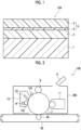
- FIG. 1 is a partial cross-sectional view schematically showing an example of a layer configuration of a photoreceptor according to the present exemplary embodiment.
- a photoreceptor 10A shown in Fig. 1 has a structure in which an undercoat layer 2, a charge generation layer 3, and a charge transport layer 4 are laminated in this order on a conductive substrate 1, and the charge generation layer 3 and the charge transport layer 4 constitute a photosensitive layer 5 (so-called function separation type photosensitive layer).
- the photoreceptor 10A may include an interlayer (not shown) between the undercoat layer 2 and the charge generation layer 3.
- the undercoat layer 2 may or may not be present.
- the photosensitive layer is typically formed by being dipped and coated with a coating solution under a condition that the axial direction of the conductive substrate is set as the gravity direction.
- the polyarylate resin is a resin that is likely to be viscous due to the molecular structure thereof (stacking of aromatic rings), and the polyarylate resin is more likely to be viscous as the molecular weight thereof increases.
- the concentration of the polyarylate resin in the coating solution is adjusted to be relatively low.
- the photoreceptor according to the present exemplary embodiment is formed such that the thickness of the charge generation layer positioned below the charge transport layer is set to be less at one end portion and greater at the other end portion, as compared with the central portion.
- the uniformity of the layer thickness of the charge transport layer is enhanced by the following mechanism in a case where the charge transport layer is dipped and coated by setting the end of the charge generation layer with a small thickness to be positioned on the upper side in the gravity direction and the end thereof with a large thickness to be positioned on the lower side in the gravity direction.
- the coating solution for forming a charge transport layer easily adheres to the upper end portion, the coating solution is suppressed from flowing down from the upper end portion, and reduction in film thickness of the upper end portion of the charge transport layer is suppressed. Further, it is considered that the coating solution for forming a charge transport layer is likely to remain on the upper end portion even in the case where the thickness of the upper end portion of the charge generation layer is less than the thickness of the central portion, and thus reduction in film thickness of the upper end portion of the charge transport layer is suppressed.
- the coating solution for forming a charge transport layer is likely to flow down in the gravity direction in a case where the thickness of the upper end portion of the charge generation layer is greater than or equal to the thickness of the central portion, and thus the thickness of the upper end portion of the charge transport layer is likely to be reduced.
- the coating solution for forming a charge transport layer easily adheres to the lower end portion, the coating solution flows down from the lower end portion, and an increase in the thickness of the lower end portion of the charge transport layer is suppressed. Further, an increase in the thickness of the lower end portion of the charge transport layer is considered to be suppressed even in the case where the thickness of the lower end portion of the charge generation layer is greater than the thickness of the central portion.
- the coating solution for forming a charge transport layer is likely to remain at a large thickness on the lower end portion in a case where the thickness of the lower end portion of the charge generation layer is less than or equal to thickness of the central portion, and thus the thickness of the lower end portion of the charge transport layer is likely to increase.
- the uniformity of the layer thickness of the charge transport layer is enhanced in a case where the thickness of the charge generation layer is less at one end portion and greater at the other end portion. As a result, it is considered that charging unevenness is unlikely to occur in the photoreceptor.
- the charge generation layer is originally a thin layer.
- the layer thickness of the charge generation layer is typically less than 1 ⁇ m, and even the maximum layer thickness is several ⁇ m. Therefore, a difference in the layer thickness of the charge generation layer in the axial direction is small, and thus the difference in the layer thickness is difficult to detect in some cases.
- the absorbance of the photosensitive layer at a wavelength of 678 nm in the absorption spectrum is employed as an index of the thickness of the charge generation layer of the photoreceptor according to the present exemplary embodiment.
- the charge generation material of the charge generation layer a charge generation material having absorption at a wavelength of 678 nm is used in many cases. It can be considered that the thickness of the charge generation layer increases as the absorbance at a wavelength of 678 nm increases and that the thickness of the charge generation layer decreases as the absorbance at a wavelength of 678 nm decreases.
- the thickness of the charge generation layer can be known by comparing the absorbances of the central portion, one end portion, and the other end portion of the photoreceptor at a wavelength of 678 nm.
- the absorption spectrum of the photosensitive layer is measured as follows.
- the photosensitive layer is peeled off and cut out from a position (M), a position (U), and a position (L) into a square with a size (axial direction ⁇ circumferential direction) of 1 cm ⁇ 1 cm.
- the position (M) is the center of the photoreceptor in the axial direction.
- the position (U) is a position of 0.40 L from the center of the photoreceptor in the axial direction toward one end.
- L represents the total length of the photoreceptor in the axial direction.
- the position (L) is a position of 0.40 L from the center of the photoreceptor in the axial direction toward the other end.
- L represents the total length of the photoreceptor in the axial direction.
- the photosensitive layer is cut out from four positions at intervals of 90° in the circumferential direction at each of the position (M), the position (U), and the position (L). Therefore, four sheets of films having a square shape with a size of 1 cm ⁇ 1 cm are obtained at each of the position (M), the position (U), and the position (L).
- a solution is prepared by dipping four sheets of films at each position in 100 mL of tetrahydrofuran.
- the absorption spectrum is measured with an ultraviolet-visible spectrophotometer (for example, Hitachi U2000) using this solution as a sample, and the absorbance at a wavelength of 678 nm is detected.
- the absorbance of the photosensitive layer at the position (M) at a wavelength of 678 nm is defined as Im.
- the absorbance of the photosensitive layer at the position (U) at a wavelength of 678 nm is defined as Iu.
- the absorbance of the photosensitive layer at the position (L) at a wavelength of 678 nm is defined as Il.
- Iu and Im have a relationship represented by Expression (1), preferably a relationship represented by Expression (1-1), more preferably a relationship represented by Expression (1-2), and still more preferably a relationship represented by Expression (1-3).
- Il and Im have a relationship represented by 1.05 ⁇ Im ⁇ Il .
- Examples of means for forming the charge generation layer such that the thickness of one end portion is adjusted to be less and the thickness of the other end portion is adjusted to be greater than the thickness of the central portion in order to satisfy Expression (1) and Expression (2) include the following means.
- the number of carbon atoms of the linear alkyl group having 4 or more and 20 or less carbon atoms as Rb 102 is, for example, preferably 4 or more and 16 or less, more preferably 4 or more and 12 or less, and still more preferably 4 or more and 8 or less.
- the alkyl group in the alkoxy group having 1 or more and 4 or less carbon atoms as Rb 113 and Rb 213 may be linear, branched, or cyclic.
- the number of carbon atoms of the alkyl group in the alkoxy group having 1 or more and 4 or less carbon atoms is, for example, preferably 1 or more and 3 or less, more preferably 1 or 2, and still more preferably 1.
- Rb 104 and Rb 204 each independently represent a hydrogen atom, an alkyl group having 1 or more and 3 or less carbon atoms
- Rb 404 , Rb 504 , Rb 804 , and Rb 904 each independently represent a hydrogen atom, an alkyl group having 1 or more and 4 or less carbon atoms, an alkoxy group having 1 or more and 6 or less carbon atoms, or a halogen atom.
- the aryl group having 6 or more and 12 or less carbon atoms as Ar 105 may be any of a monocycle or a polycycle.
- the number of carbon atoms of the aryl group is, for example, preferably 6 or more and 10 or less and more preferably 6.
- the number of carbon atoms of the linear alkyl group having 1 or more and 3 or less carbon atoms as Rb 116 and Rb 216 is, for example, preferably 1 or 2 and more preferably 1. Specific examples of such a group include a methyl group, an ethyl group, and an n-propyl group.
- the alkyl group in the alkoxy group having 1 or more and 4 or less carbon atoms as Rb 116 and Rb 216 may be linear, branched, or cyclic.
- the number of carbon atoms of the alkyl group in the alkoxy group having 1 or more and 4 or less carbon atoms is, for example, preferably 1 or more and 3 or less, more preferably 1 or 2, and still more preferably 1.
- Such a group include a methoxy group, an ethoxy group, an n-propoxy group, an n-butoxy group, an isopropoxy group, an isobutoxy group, a sec-butoxy group, a tert-butoxy group, a cyclopropoxy group, and a cyclobutoxy group.
- halogen atom examples include a fluorine atom, a chlorine atom, a bromine atom, and an iodine atom.
- Rb 408 , Rb 508 , Rb 808 , and Rb 908 each independently represent a hydrogen atom, an alkyl group having 1 or more and 4 or less carbon atoms, an alkoxy group having 1 or more and 6 or less carbon atoms, or a halogen atom.
- Examples of the cyclic alkyl group having 3 or 4 carbon atoms include a cyclopropyl group and a cyclobutyl group.
- the alkyl group having 1 or more and 4 or less carbon atoms as Rb 900 may be any of linear, branched, or cyclic.
- the number of carbon atoms of the alkyl group is, for example, preferably 1 or more and 3 or less, more preferably 1 or 2, and still more preferably 1.
- linear alkyl group having 1 or more and 4 or less carbon atoms examples include a methyl group, an ethyl group, an n-propyl group, and an n-butyl group.
- Examples of the cyclic alkoxy group having 3 or more and 6 or less carbon atoms include a cyclopropoxy group, a cyclobutoxy group, a cyclopentyloxy group, and a cyclohexyloxy group.
- halogen atom as Rb 900 examples include a fluorine atom, a chlorine atom, a bromine atom, and an iodine atom.
- diol units (B1-1) to (B1-6) are shown as specific examples of the diol unit (B1).
- the diol unit (B1) is not limited thereto.
- diol units (B2-1) to (B2-11) are shown as specific examples of the diol unit (B2).
- the diol unit (B2) is not limited thereto.
- diol units (B4-1) to (B4-7) are shown as specific examples of the diol unit (B4).
- the diol unit (B4) is not limited thereto.
- diol units (B6-1) to (B6-4) are shown as specific examples of the diol unit (B6).
- the diol unit (B6) is not limited thereto.
- diol units (B7-1) to (B7-3) are shown as specific examples of the diol unit (B7).
- the diol unit (B7) is not limited thereto.
- diol units (B8-1) to (B8-3) are shown as specific examples of the diol unit (B8).
- the diol unit (B8) is not limited thereto.
- the mass proportion of the diol unit (B) in the polyarylate resin (1) is, for example, preferably 25% by mass or greater and 80% by mass or less.
- the mass proportion of the diol unit (B) is 25% by mass or greater, peeling of the photosensitive layer can be further suppressed.
- the mass proportion of the diol unit (B) is, for example, more preferably 30% by mass or greater and still more preferably 35% by mass or greater.
- the mass proportion of the diol unit (B) is 80% by mass or less, the solubility in a coating solution for forming the photosensitive layer is maintained, and thus the abrasion resistance can be improved.
- the mass proportion of the diol unit (B) is, for example, more preferably 75% by mass or less and still more preferably 70% by mass or less.
- diol units in addition to the diol unit (B) include aliphatic diol (such as ethylene glycol, diethylene glycol, triethylene glycol, propylene glycol, butanediol, hexanediol, and neopentyl glycol) units and alicyclic diol (such as cyclohexanediol, cyclohexane dimethanol, and hydrogenated bisphenol A) units.
- aliphatic diol such as ethylene glycol, diethylene glycol, triethylene glycol, propylene glycol, butanediol, hexanediol, and neopentyl glycol
- alicyclic diol such as cyclohexanediol, cyclohexane dimethanol, and hydrogenated bisphenol A
- Examples of the monohydric phenol include phenol, o-cresol, m-cresol, p-cresol, o-ethylphenol, m-ethylphenol, p-ethylphenol, o-propylphenol, m-propylphenol, p-propylphenol, o-tert-butylphenol, m-tert-butylphenol, p-tert-butylphenol, pentylphenol, hexylphenol, octylphenol, nonylphenol, a 2,6-dimethylphenol derivative, a 2-methylphenol derivative, o-phenylphenol, m-phenylphenol, p-phenylphenol, o-methoxyphenol, m-methoxyphenol, p-methoxyphenol, 2,3,5-trimethylphenol, 2,3,6-trimethylphenol, 2,3-xylenol, 2,4-xylenol, 2,5-xylenol, 2,6
- Examples of the monovalent acid chloride include monofunctional acid halides such as benzoyl chloride, benzoic acid chloride, methanesulfonyl chloride, phenylchloroformate, acetic acid chloride, butyric acid chloride, octyl acid chloride, benzenesulfonyl chloride, benzenesulfinyl chloride, sulfinyl chloride, benzene phosphonyl chloride, and substituents thereof.
- monofunctional acid halides such as benzoyl chloride, benzoic acid chloride, methanesulfonyl chloride, phenylchloroformate, acetic acid chloride, butyric acid chloride, octyl acid chloride, benzenesulfonyl chloride, benzenesulfinyl chloride, sulfinyl chloride, benzene phosphonyl chloride, and substituents thereof
- Examples of the monohydric alcohol include methanol, ethanol, n-propanol, isopropanol, n-butanol, 2-butanol, pentanol, hexanol, dodecyl alcohol, stearyl alcohol, benzyl alcohol, and phenethyl alcohol.
- the film thickness of the anodized film is, for example, preferably 0.3 ⁇ m or greater and 15 ⁇ m or less. In a case where the film thickness is in the above-described range, the barrier properties against injection tend to be exhibited, and an increase in the residual potential due to repeated use tends to be suppressed.
- the boehmite treatment is carried out, for example, by dipping the conductive substrate in pure water at 90°C or higher and 100°C or lower for 5 minutes to 60 minutes or by bringing the conductive substrate into contact with heated steam at 90°C or higher and 120°C or lower for 5 minutes to 60 minutes.
- the film thickness of the coating film is, for example, preferably 0.1 ⁇ m or greater and 5 ⁇ m or less.
- This coating film may be further subjected to the anodizing treatment using an electrolytic solution having low film solubility, such as adipic acid, boric acid, a borate, a phosphate, a phthalate, a maleate, a benzoate, a tartrate, or a citrate.
- examples of the inorganic particles include inorganic particles having a powder resistance (volume resistivity) of 1 ⁇ 10 2 ⁇ cm or greater and 1 ⁇ 10 11 ⁇ cm or less.
- the inorganic particles having the above-described resistance value for example, metal oxide particles such as tin oxide particles, titanium oxide particles, zinc oxide particles, and zirconium oxide particles may be used, and zinc oxide particles are particularly preferable.
- the specific surface area of the inorganic particles measured by the BET method may be, for example, 10 m 2 /g or greater.
- the volume average particle diameter of the inorganic particles may be, for example, 50 nm or greater and 2,000 nm or less (for example, preferably 60 nm or greater and 1,000 nm or less).
- the content of the inorganic particles is, for example, preferably 10% by mass or greater and 80% by mass or less and more preferably 40% by mass or greater and 80% by mass or less with respect to the amount of the binder resin.
- the surface treatment agent examples include a silane coupling agent, a titanate-based coupling agent, an aluminum-based coupling agent, and a surfactant.
- a silane coupling agent is preferable, and a silane coupling agent containing an amino group is more preferable.
- silane coupling agent containing an amino group examples include 3-aminopropyltriethoxysilane, N-2-(aminoethyl)-3-aminopropyltrimethoxysilane, N-2-(aminoethyl)-3-aminopropylmethyldimethoxysilane, and N,N-bis(2-hydroxyethyl)-3-aminopropyltriethoxysilane, but are not limited thereto.
- the silane coupling agent may be used in the form of a mixture of two or more kinds thereof.
- a silane coupling agent containing an amino group and another silane coupling agent may be used in combination.
- other silane coupling agents include vinyltrimethoxysilane, 3-methacryloxypropyl-tris(2-methoxyethoxy)silane, 2-(3,4-epoxycyclohexyl)ethyltrimethoxysilane, 3-glycidoxypropyltrimethoxysilane, vinyltriacetoxysilane, 3-mercaptopropyltrimethoxysilane, 3-aminopropyltriethoxysilane, N-2-(aminoethyl)-3-aminopropyltrimethoxysilane, N-2-(aminoethyl)-3-aminopropylmethyldimethoxysilane, N,N-bis(2-hydroxyethyl)-3-aminopropyltrie
- the undercoat layer may contain an electron-accepting compound (acceptor compound) together with the inorganic particles from the viewpoint of enhancing the long-term stability of the electrical properties and the carrier blocking properties.
- the electron-accepting compound examples include electron-transporting substances, for example, a quinone-based compound such as chloranil or bromanil; a tetracyanoquinodimethane-based compound; a fluorenone compound such as 2,4,7-trinitrofluorenone or 2,4,5,7-tetranitro-9-fluorenone; an oxadiazole-based compound such as 2-(4-biphenyl)-5-(4-t-butylphenyl)-1,3,4-oxadiazole, 2,5-bis(4-naphthyl)-1,3,4-oxadiazole, or 2,5-bis(4-diethylaminophenyl)-1,3,4-oxadiazole; a xanthone-based compound; a thiophene compound; a diphenoquinone compound such as 3,3',5,5'-tetra-t-butyldiphenoquinone; and a benzophenone compound.
- a compound having an anthraquinone structure is preferable.
- a compound having an anthraquinone structure for example, a hydroxyanthraquinone compound, an aminoanthraquinone compound, or an aminohydroxyanthraquinone compound is preferable, and specifically, for example, anthraquinone, alizarin, quinizarin, anthrarufin, or purpurin is preferable.
- the electron-accepting compound may be contained in the undercoat layer in a state of being dispersed with inorganic particles or in a state of being attached to the surface of each inorganic particle.
- Examples of the method of attaching the electron-accepting compound to the surface of the inorganic particle include a dry method and a wet method.
- the dry method is, for example, a method of attaching the electron-accepting compound to the surface of each inorganic particle by adding the electron-accepting compound dropwise to inorganic particles directly or by dissolving the electron-accepting compound in an organic solvent while stirring the inorganic particles with a mixer having a large shearing force and spraying the mixture together with dry air or nitrogen gas.
- the electron-accepting compound may be added dropwise or sprayed, for example, at a temperature lower than or equal to the boiling point of the solvent. After the dropwise addition or the spraying of the electron-accepting compound, the compound may be further baked at 100°C or higher. The baking is not particularly limited as long as the temperature and the time are adjusted such that the electrophotographic characteristics can be obtained.
- the wet method is, for example, a method of attaching the electron-accepting compound to the surface of each inorganic particle by adding the electron-accepting compound to inorganic particles while dispersing the inorganic particles in a solvent by performing stirring or using ultrasonic waves, a sand mill, an attritor, or a ball mill, stirring or dispersing the mixture, and removing the solvent.
- the solvent removing method is carried out by, for example, filtration or distillation so that the solvent is distilled off.
- the mixture may be further baked at 100°C or higher. The baking is not particularly limited as long as the temperature and the time are adjusted such that the electrophotographic characteristics can be obtained.
- the moisture contained in the inorganic particles may be removed before the electron-accepting compound is added, and examples thereof include a method of removing the moisture while stirring and heating the moisture in a solvent and a method of removing the moisture by azeotropically boiling the moisture with a solvent.
- the electron-accepting compound may be attached to the surface before the inorganic particles are subjected to a surface treatment with a surface treatment agent or simultaneously with the surface treatment performed on the inorganic particles with a surface treatment agent.
- the content of the electron-accepting compound may be, for example, 0.01% by mass or greater and 20% by mass or less and preferably 0.01% by mass or greater and 10% by mass or less with respect to the amount of the inorganic particles.
- binder resin used for the undercoat layer examples include known polymer compounds such as an acetal resin (such as polyvinyl butyral), a polyvinyl alcohol resin, a polyvinyl acetal resin, a casein resin, a polyamide resin, a cellulose resin, gelatin, a polyurethane resin, a polyester resin, an unsaturated polyester resin, a methacrylic resin, an acrylic resin, a polyvinyl chloride resin, a polyvinyl acetate resin, a vinyl chloride-vinyl acetate-maleic anhydride resin, a silicone resin, a silicone-alkyd resin, a urea resin, a phenol resin, a phenol-formaldehyde resin, a melamine resin, a urethane resin, an alkyd resin, and an epoxy resin; a zirconium chelate compound; a titanium chelate compound; an aluminum chelate compound; a titanium alkoxide compound; an organic titanium compound;
- binder resin used for the undercoat layer examples include a charge-transporting resin containing a charge-transporting group, and a conductive resin (such as polyaniline).
- the binder resin used for the undercoat layer for example, a resin insoluble in a coating solvent of the upper layer is preferable, and a resin obtained by reaction between a curing agent and at least one resin selected from the group consisting of a thermosetting resin such as a urea resin, a phenol resin, a phenol-formaldehyde resin, a melamine resin, a urethane resin, an unsaturated polyester resin, an alkyd resin, or an epoxy resin; a polyamide resin, a polyester resin, a polyether resin, a methacrylic resin, an acrylic resin, a polyvinyl alcohol resin, and a polyvinyl acetal resin is particularly preferable.
- a thermosetting resin such as a urea resin, a phenol resin, a phenol-formaldehyde resin, a melamine resin, a urethane resin, an unsaturated polyester resin, an alkyd resin, or an epoxy resin
- a polyamide resin a polyester resin
- binder resins are used in combination of two or more kinds thereof, the mixing ratio thereof is set as necessary.
- the undercoat layer may contain various additives for improving the electrical properties, the environmental stability, and the image quality.
- the interlayer is, for example, a layer containing a resin.
- the resin used for the interlayer include a polymer compound, for example, an acetal resin (such as polyvinyl butyral), a polyvinyl alcohol resin, a polyvinyl acetal resin, a casein resin, a polyamide resin, a cellulose resin, gelatin, a polyurethane resin, a polyester resin, a methacrylic resin, an acrylic resin, a polyvinyl chloride resin, a polyvinyl acetate resin, a vinyl chloride-vinyl acetate-maleic anhydride resin, a silicone resin, a silicone-alkyd resin, a phenol-formaldehyde resin, or a melamine resin.
- an acetal resin such as polyvinyl butyral
- a polyvinyl alcohol resin such as polyvinyl butyral
- a polyvinyl acetal resin such as polyvinyl alcohol resin
- the interlayer may be a layer containing an organometallic compound.
- organometallic compound used for the interlayer include an organometallic compound containing metal atoms such as zirconium, titanium, aluminum, manganese, and silicon.
- the formation of the interlayer is not particularly limited, and a known forming method is used.
- a coating film of a coating solution for forming an interlayer in which the above-described components are added to a solvent is formed, and the coating film is dried and, as necessary, heated.
- a metal phthalocyanine pigment or a metal-free phthalocyanine pigment is preferably used as the charge generation material in order to deal with laser exposure in a near infrared region.
- at least one selected from the group consisting of hydroxygallium phthalocyanine, chlorogallium phthalocyanine, dichlorotin phthalocyanine, and titanyl phthalocyanine is preferable, hydroxygallium phthalocyanine and/or chlorogallium phthalocyanine is more preferable, and hydroxygallium phthalocyanine is still more preferable.
- Hydroxygallium phthalocyanine has an absorption peak at a wavelength of 678 nm.
- a fused ring aromatic pigment such as dibromoanthanthrone; a thioindigo-based pigment; a porphyrazine compound; zinc oxide; trigonal selenium; or a bisazo pigment is preferable as the charge generation material in order to deal with laser exposure in a near ultraviolet region.
- the above-described charge generation material may also be used even in a case where an incoherent light source such as an LED or an organic EL image array having a center wavelength of light emission at 450 nm or greater and 780 nm or less is used, but from the viewpoint of the resolution, the electric field intensity in the photosensitive layer is increased, and a decrease in charge due to injection of a charge from the substrate, that is, image defects referred to as so-called black spots are likely to occur when a thin film having a thickness of 20 ⁇ m or less is used as the photosensitive layer.
- the above-described tendency is evident when a p-type semiconductor such as trigonal selenium or a phthalocyanine pigment is used as the charge generation material that is likely to generate a dark current.
- n-type semiconductor such as a fused ring aromatic pigment, a perylene pigment, or an azo pigment
- a dark current is unlikely to be generated, and image defects referred to as black spots can be suppressed even in a case where a thin film is used as the photosensitive layer.
- the n-type is determined by the polarity of the flowing photocurrent using a typically used time-of-flight method, and a material in which electrons more easily flow as carriers than positive holes is determined as the n-type.
- the binder resin used for the charge generation layer is selected from a wide range of insulating resins, and the binder resin may be selected from organic photoconductive polymers such as poly-N-vinylcarbazole, polyvinyl anthracene, polyvinylpyrene, and polysilane.
- binder resin examples include a polyvinyl butyral resin, a polyarylate resin (a polycondensate of bisphenols and aromatic divalent carboxylic acid), a polycarbonate resin, a polyester resin, a phenoxy resin, a vinyl chloride-vinyl acetate copolymer, a polyamide resin, an acrylic resin, a polyacrylamide resin, a polyvinylpyridine resin, a cellulose resin, a urethane resin, an epoxy resin, casein, a polyvinyl alcohol resin, and a polyvinylpyrrolidone resin.
- the term "insulating" denotes that the volume resistivity is 1 ⁇ 10 13 ⁇ cm or greater.
- binder resins may be used alone or in the form of a mixture of two or more kinds thereof.
- the blending ratio between the charge generation material and the binder resin is, for example, preferably in a range of 10:1 to 1:10 in terms of the mass ratio.
- the charge generation layer may also contain other known additives.
- the formation of the charge generation layer is not particularly limited, and a known forming method is used.
- a coating film of a coating solution for forming a charge generation layer in which the above-described components are added to a solvent is formed, and the coating film is dried and, as necessary, heated.
- the charge generation layer may be formed by vapor deposition of the charge generation material.
- the formation of the charge generation layer by vapor deposition is, for example, particularly appropriate in a case where a fused ring aromatic pigment or a perylene pigment is used as the charge generation material.
- Examples of the solvent for preparing the coating solution for forming a charge generation layer include methanol, ethanol, n-propanol, n-butanol, benzyl alcohol, methyl cellosolve, ethyl cellosolve, acetone, methyl ethyl ketone, cyclohexanone, methyl acetate, n-butyl acetate, dioxane, tetrahydrofuran, methylene chloride, chloroform, chlorobenzene, and toluene. These solvents are used alone or in the form of a mixture of two or more kinds thereof.
- a media disperser such as a ball mill, a vibration ball mill, an attritor, a sand mill, or a horizontal sand mill, or a medialess disperser such as a stirrer, an ultrasonic disperser, a roll mill, or a high-pressure homogenizer is used.
- the high-pressure homogenizer examples include a collision type high-pressure homogenizer in which a dispersion liquid is dispersed by a liquid-liquid collision or a liquid-wall collision in a high-pressure state, and a penetration type high-pressure homogenizer in which a dispersion liquid is dispersed by causing the dispersion liquid to penetrate through a fine flow path in a high-pressure state.
- the dispersion it is effective to set the average particle diameter of the charge generation material in the coating solution for forming a charge generation layer to 0.5 ⁇ m or less, for example, preferably 0.3 ⁇ m or less, and more preferably 0.15 ⁇ m or less.
- Examples of the method of coating the undercoat layer (or the interlayer) with the coating solution for forming a charge generation layer include typical methods such as a dip coating method, a blade coating method, a wire bar coating method, a spray coating method, a bead coating method, an air knife coating method, and a curtain coating method.
- a dip coating method is preferable as a method of forming the charge generation layer.
- the average thickness of the charge generation layer is, for example, set to be in a range of 0.05 ⁇ m or greater and 5.0 ⁇ m or less, a range of 0.10 ⁇ m or greater and 2.0 ⁇ m or less, or a range of 0.15 ⁇ m or greater and 1.0 ⁇ m or less.
- the charge transport layer is, for example, a layer containing a charge transport material and a binder resin.
- the charge transport layer may be a layer containing a polymer charge transport material.
- the charge transport material examples include a quinone-based compound such as p-benzoquinone, chloranil, bromanil, or anthraquinone; a tetracyanoquinodimethane-based compound; a fluorenone compound such as 2,4,7-trinitrofluorenone; a xanthone compound; a benzophenone-based compound; a cyanovinyl-based compound; and an electron-transporting compound such as an ethylene-based compound.
- a quinone-based compound such as p-benzoquinone, chloranil, bromanil, or anthraquinone
- a tetracyanoquinodimethane-based compound examples include a fluorenone compound such as 2,4,7-trinitrofluorenone; a xanthone compound; a benzophenone-based compound; a cyanovinyl-based compound; and an electron-transporting compound such as an ethylene-based compound.
- R T5 and R T6 represent an aryl group
- R 51 , R 52 , R 61 , and R 62 each independently represent a hydrogen atom or an alkyl group having 1 or more and 3 or less carbon atoms.
- the group in Formula (C1) may be substituted with a halogen atom, an alkyl group having 1 or more and 5 or less carbon atoms, an alkoxy group having 1 or more and 5 or less carbon atoms, or a substituted amino group substituted with an alkyl group having 1 or more and 3 or less carbon atoms.
- R T21 , R T22 , R T23 , R T24 , and R T25 each independently represent a hydrogen atom, an alkyl group, or an aryl group.
- the proportion of the polyarylate resin (1) in the total amount of the binder resin contained in the charge transport layer is, for example, preferably 60% by mass or greater, more preferably 70% by mass or greater, still more preferably 80% by mass or greater, and particularly preferably 90% by mass or greater.
- the proportion of the polyarylate resin (1) in the total amount of the binder resin contained in the charge transport layer is, for example, preferably 60% by mass or greater, more preferably 70% by mass or greater, still more preferably 80% by mass or greater, and particularly preferably 90% by mass or greater.
- the charge transport layer contains the polyarylate resin and a polycarbonate resin as the binder resin.
- the mass ratio of both resins is, for example, preferably in a range of 95:5 to 40:60.
- the mass ratio of both resins is, for example, preferably in a range of 95:5 to 40:60.
- polycarbonate resin for example, a polycarbonate resin with continuous constitutional units having an aromatic ring is preferable, and specific examples thereof include polycarbonate resins used in examples described below.
- the charge transport layer may contain other binder resins in addition to the polyarylate resin and the polycarbonate resin.
- binder resins include a polyester resin other than the polyarylate resin, a methacrylic resin, an acrylic resin, a polyvinyl chloride resin, a polyvinylidene chloride resin, a polystyrene resin, a polyvinyl acetate resin, a styrene-butadiene copolymer, a vinylidene chloride-acrylonitrile copolymer, a vinyl chloride-vinyl acetate copolymer, a vinyl chloride-vinyl acetate-maleic anhydride copolymer, a silicone resin, a silicone alkyd resin, a phenol-formaldehyde resin, a styrene-alkyd resin, poly-N-vinylcarbazole, and polysilane.
- binder resins may be used alone or in combination of two or more kinds thereof.
- the charge transport layer may also contain other known additives.
- the additives include an antioxidant, a leveling agent, an antifoaming agent, a filler, and a viscosity adjuster.
- the formation of the charge transport layer is not particularly limited, and a known forming method is used.
- a coating film of a coating solution for forming a charge transport layer in which the above-described components are added to a solvent is formed, and the coating film is dried and, as necessary, heated.
- Examples of the solvent for preparing the coating solution for forming a charge transport layer include typical organic solvents, for example, aromatic hydrocarbons such as benzene, toluene, xylene, and chlorobenzene; ketones such as acetone and 2-butanone; halogenated aliphatic hydrocarbons such as methylene chloride, chloroform, and ethylene chloride; and cyclic or linear ethers such as tetrahydrofuran and ethyl ether. These solvents are used alone or in the form of a mixture of two or more kinds thereof.
- aromatic hydrocarbons such as benzene, toluene, xylene, and chlorobenzene
- ketones such as acetone and 2-butanone
- halogenated aliphatic hydrocarbons such as methylene chloride, chloroform, and ethylene chloride
- cyclic or linear ethers such as tetrahydrofuran and ethyl ether.
- Examples of the coating method of coating the charge generation layer with the coating solution for forming a charge transport layer include typical methods such as a dip coating method, a blade coating method, a wire bar coating method, a spray coating method, a bead coating method, an air knife coating method, and a curtain coating method.
- a dip coating method is preferable as a method of forming the charge transport layer.
- the average thickness of the charge transport layer is, for example, 30 ⁇ m or greater, preferably 34 ⁇ m or greater, and more preferably 38 ⁇ m or greater.
- the average thickness of the charge transport layer is, for example, preferably 50 ⁇ m or less, more preferably 47 ⁇ m or less, and still more preferably 45 ⁇ m or less.
- a layer formed of a cured film may be applied to the protective layer.
- these layers include the layers described in the items 1) and 2) below.
- Examples of the reactive group of the reactive group-containing charge transport material include known reactive groups such as a chain polymerizable group, an epoxy group, -OH, -OR [here, R represents an alkyl group], -NH 2 , -SH, -COOH, and -SiR Q1 3-Qn (OR Q2 ) Qn [here, R Q1 represents a hydrogen atom, an alkyl group, or a substituted or unsubstituted aryl group, R Q2 represents a hydrogen atom, an alkyl group, or a trialkylsilyl group, and Qn represents an integer of 1 to 3].
- a chain polymerizable group such as a chain polymerizable group, an epoxy group, -OH, -OR [here, R represents an alkyl group], -NH 2 , -SH, -COOH, and -SiR Q1 3-Qn (OR Q2 ) Qn
- R Q1 represents a hydrogen atom, an alky
- the chain polymerizable group is not particularly limited as long as the group is a functional group capable of radical polymerization and is, for example, a functional group containing a group having at least a carbon double bond. Specific examples thereof include a vinyl group, a vinyl ether group, a vinyl thioether group, a phenyl vinyl group, a vinyl phenyl group, an acryloyl group, a methacryloyl group, and a group containing at least one selected from derivatives thereof.
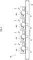
- An image forming apparatus includes the electrophotographic photoreceptor, a charging device that charges a surface of the electrophotographic photoreceptor, an electrostatic latent image forming device that forms an electrostatic latent image on the charged surface of the electrophotographic photoreceptor, a developing device that develops the electrostatic latent image formed on the surface of the electrophotographic photoreceptor with a developer containing a toner to form a toner image, and a transfer device that transfers the toner image to a surface of a recording medium.
- the electrophotographic photoreceptor according to the present exemplary embodiment is employed as the electrophotographic photoreceptor.
- known image forming apparatuses such as an apparatus including a fixing device that fixes the toner image transferred to the surface of a recording medium; a direct transfer type apparatus that transfers the toner image formed on the surface of the electrophotographic photoreceptor directly to the recording medium; an intermediate transfer type apparatus that primarily transfers the toner image formed on the surface of the electrophotographic photoreceptor to the surface of the intermediate transfer member and secondarily transfers the toner image transferred to the surface of the intermediate transfer member to the surface of the recording medium; an apparatus including a cleaning device that cleans the surface of the electrophotographic photoreceptor after the transfer of the toner image and before the charging; an apparatus including a charge erasing device that erases the charges on the surface of the electrophotographic photoreceptor by applying the charge erasing light after the transfer of the toner image and before the charging; and an apparatus including an electrophotographic photoreceptor heating member for increasing the temperature of the electrophotographic photoreceptor and decreasing the relative temperature are employed
- intermediate transfer member 50 a belt-like intermediate transfer member (intermediate transfer belt) containing semi-conductive polyimide, polyamide-imide, polycarbonate, polyarylate, polyester, rubber, or the like is used. Further, as the form of the intermediate transfer member, a drum-like intermediate transfer member may be used in addition to the belt-like intermediate transfer member.
- Iu/Im/Il in Table 2 denotes a relative value in a case where the value of Im is set to 1.
- Table 2 Charge transport layer Photosensitive layer Performance of photoreceptor Average thickness Polyarylate resin Polycarbonate resin Mixing ratio between polyarylate and polycarbonate Absorbance at wavelength of 678 nm Iu/Im/Il Abrasion resistance Charging unevenness ⁇ m Type Mw Type Mass ratio - - - Comparative example 1 42 (1-1) 110 ⁇ 10 3 - 100:0 1.00/1/1.00 A c Example 5 42 (1-1) 110 ⁇ 10 3 - 100:0 0.95/1/1.05 A B Example 4 42 (1-1) 110 ⁇ 10 3 - 100:0 0.90/1/1.10 A B Example 3 42 (1-1) 110 ⁇ 10 3 - 100:0 0.85/1/1.15 A A Example 1 42 (1-1) 110 ⁇ 10 3 - 100:0 0.80/1/1.20 A A Example 2 42 (1-1) 110 ⁇ 10 3 - 100:0 0.75/1/1.25 A B Example 6 42
- the electrophotographic photoreceptor, the process cartridge, and the image forming apparatus of the present disclosure include the following aspects.
- Each formula representing a compound is the same as the formula having the same number described below.
Landscapes
- Physics & Mathematics (AREA)
- General Physics & Mathematics (AREA)
- Chemical & Material Sciences (AREA)
- Chemical Kinetics & Catalysis (AREA)
- Spectroscopy & Molecular Physics (AREA)
- Engineering & Computer Science (AREA)
- Computer Vision & Pattern Recognition (AREA)
- Photoreceptors In Electrophotography (AREA)
Claims (11)
- Elektrophotographischer Photorezeptor, umfassend:ein leitfähiges Substrat; undeine lichtempfindliche Schicht, die auf dem leitfähigen Substrat angeordnet ist und eine Ladungserzeugungsschicht und eine Ladungstransportschicht enthält, wobei die Ladungserzeugungsschicht Hydroxygallium-Phthalocyanin enthält,wobei die Ladungstransportschicht eine durchschnittliche Dicke von 30 µm oder mehr aufweist,die Ladungstransportschicht ein Polyarylatharz enthält, undein Absorptionsspektrum, das durch Abziehen der lichtempfindlichen Schicht undLösen der lichtempfindlichen Schicht in Tetrahydrofuran gemessen wird, Ausdruck (1) und Ausdruck (2) erfüllt,

 in einem Fall, in dem eine Gesamtlänge des elektrophotographischen Photorezeptors in einer Axialrichtung als L definiert ist,Im eine Absorption der lichtempfindlichen Schicht bei einer Wellenlänge von 678 nm darstellt, die von einer Mitte der Gesamtlänge des elektrophotographischen Photorezeptors in der Achsrichtung abgezogen wird,Iu eine Absorption der lichtempfindlichen Schicht bei einer Wellenlänge von 678 nm darstellt, die an einer Position von 0,40 L von der Mitte der Gesamtlänge des elektrophotographischen Photorezeptors in der Achsrichtung zu einem Ende hin abgezogen wird,Il eine Absorption der lichtempfindlichen Schicht bei einer Wellenlänge von 678 nm darstellt, die an einer Position von 0,40 L von der Mitte der Gesamtlänge des elektrophotographischen Photorezeptors in der Achsrichtung zu dem anderen Ende hin abgezogen wird,wobei die Absorption der lichtempfindlichen Schicht bei einer Wellenlänge von 678 nm gemäß einem Messverfahren, wie in Absatz [0029] der Beschreibung beschrieben, gemessen wird.
 - Elektrophotographischer Photorezeptor nach Anspruch 1,
wobei das Absorptionsspektrum, das durch Abziehen der lichtempfindlichen Schicht und Lösen der lichtempfindlichen Schicht in Tetrahydrofuran gemessen wird, Ausdruck (1-3) und Ausdruck (2-3) erfüllt,
 in einem Fall, in dem die Gesamtlänge des elektrophotographischen Photorezeptors in der Axialrichtung als L definiert ist,Im die Absorption der lichtempfindlichen Schicht bei einer Wellenlänge von 678 nm darstellt, die von der Mitte der Gesamtlänge des elektrophotographischen Photorezeptors in der Achsrichtung abgezogen wird,Iu die Absorption der lichtempfindlichen Schicht bei einer Wellenlänge von 678 nm darstellt, die an einer Position von 0,40 L von der Mitte der Gesamtlänge des elektrophotographischen Photorezeptors in der Achsrichtung zu einem Ende hin abgezogen wird,Il die Absorption der lichtempfindlichen Schicht bei einer Wellenlänge von 678 nm darstellt, die an einer Position von 0,40 L von der Mitte der Gesamtlänge des elektrophotographischen Photorezeptors in der Achsrichtung zu dem anderen Ende hin abgezogen wird.
 - Elektrophotographischer Photorezeptor nach Anspruch 1 oder 2,
wobei das in der Ladungstransportschicht enthaltene Polyarylatharz ein gewichtsmittleres Molekulargewicht von 80.000 oder mehr aufweist, wie durch GPC in Bezug auf Polystyrol und unter Verwendung von Tetrahydrofuran als einem Eluent gemessen. - Elektrophotographischer Photorezeptor nach einem der Ansprüche 1 bis 3,
wobei die Ladungstransportschicht ferner ein Polycarbonatharz enthält. - Elektrophotographischer Photorezeptor nach einem der Ansprüche 1 bis 4,
wobei das Polyarylatharz ein Polyarylatharz (1), das eine Dicarbonsäureeinheit (A), die durch Formel (A) dargestellt wird, und eine Dioleinheit (B), die durch Formel (B) dargestellt wird, aufweist, enthält,
 in Formel (A) ArA1 und ArA2 jeweils unabhängig voneinander einen aromatischen Ring darstellen, der einen Substituenten aufweisen kann, LA eine Einfachbindung oder eine divalente Verknüpfungsgruppe darstellt und nA1 0, 1 oder 2 darstellt,in Formel (B) ArB1 und ArB2 jeweils unabhängig voneinander einen aromatischen Ring darstellen, der einen Substituenten aufweisen kann, LB eine Einfachbindung, ein Sauerstoffatom, ein Schwefelatom oder -C(Rb1)(Rb2)- darstellt, nB1 0, 1 oder 2 darstellt, Rb1 und Rb2 jeweils unabhängig voneinander ein Wasserstoffatom, eine Alkylgruppe mit 1 oder mehr und 20 oder weniger Kohlenstoffatomen, eine Arylgruppe mit 6 oder mehr und 12 oder weniger Kohlenstoffatomen oder eine Aralkylgruppe mit 7 oder mehr und 20 oder weniger Kohlenstoffatomen darstellen und Rb1 und Rb2 aneinander gebunden sein können, um eine cyclische Alkylgruppe zu bilden.
 - Elektrophotographischer Photorezeptor nach Anspruch 5,
wobei das Polyarylatharz (1) die Dicarbonsäureeinheit (A) mit mindestens einer, die aus der Gruppe, die aus einer Dicarbonsäureeinheit (A1), die durch Formel (A1) dargestellt wird, einer Dicarbonsäureeinheit (A2), die durch Formel (A2) dargestellt wird, einer Dicarbonsäureeinheit (A3), die durch Formel (A3) dargestellt wird, und einer Dicarbonsäureeinheit (A4), die durch Formel (A4) dargestellt wird, besteht, ausgewählt wird, aufweist,


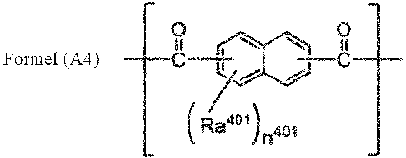 in Formel (A1) n101 eine ganze Zahl von 0 oder größer und 4 oder kleiner darstellt und n101 Stücke von Ra101 jeweils unabhängig voneinander eine Alkylgruppe mit 1 oder mehr und 10 oder weniger Kohlenstoffatomen, eine Arylgruppe mit 6 oder mehr und 12 oder weniger Kohlenstoffatomen oder eine Alkoxygruppe mit 1 oder mehr und 6 oder weniger Kohlenstoffatomen darstellen,in Formel (A2) n201 und n202 jeweils unabhängig voneinander eine ganze Zahl von 0 oder größer und 4 oder kleiner darstellen und n211 Stücke von Ra201 und n202 Stücke von Ra202 jeweils unabhängig voneinander eine Alkylgruppe mit 1 oder mehr und 10 oder weniger Kohlenstoffatomen, eine Arylgruppe mit 6 oder mehr und 12 oder weniger Kohlenstoffatomen oder eine Alkoxygruppe mit 1 oder mehr und 6 oder weniger Kohlenstoffatomen darstellen,in Formel (A3) n301 und n302 jeweils unabhängig voneinander eine ganze Zahl von 0 oder größer und 4 oder kleiner darstellen und n301 Stücke von Ra301 und n302 Stücke von Ra302 jeweils unabhängig voneinander eine Alkylgruppe mit 1 oder mehr und 10 oder weniger Kohlenstoffatomen, eine Arylgruppe mit 6 oder mehr und 12 oder weniger Kohlenstoffatomen oder eine Alkoxygruppe mit 1 oder mehr und 6 oder weniger Kohlenstoffatomen darstellen,in Formel (A4) n401 eine ganze Zahl von 0 oder größer und 6 oder kleiner darstellt und n401 Stücke von Ra401 jeweils unabhängig voneinander eine Alkylgruppe mit 1 oder mehr und 10 oder weniger Kohlenstoffatomen, eine Arylgruppe mit 6 oder mehr und 12 oder weniger Kohlenstoffatomen oder eine Alkoxygruppe mit 1 oder mehr und 6 oder weniger Kohlenstoffatomen darstellen.
 - Elektrophotographischer Photorezeptor nach Anspruch 5 oder 6,
wobei das Polyarylatharz (1) die Dioleinheit (B) mit mindestens einer, die aus der Gruppe, die aus einer Dioleinheit (B1), die durch Formel (B1) dargestellt wird, einer Dioleinheit (B2), die durch Formel (B2) dargestellt wird, einer Dioleinheit (B3), die durch Formel (B3) dargestellt wird, einer Dioleinheit (B4), die durch Formel (B4) dargestellt wird, einer Dioleinheit (B5), die durch Formel (B5) dargestellt wird, einer Dioleinheit (B6), die durch Formel (B6) dargestellt wird, einer Dioleinheit (B7), die durch Formel (B7) dargestellt wird, und einer Dioleinheit (B8), die durch Formel (B8) dargestellt wird, besteht, ausgewählt wird, aufweist,


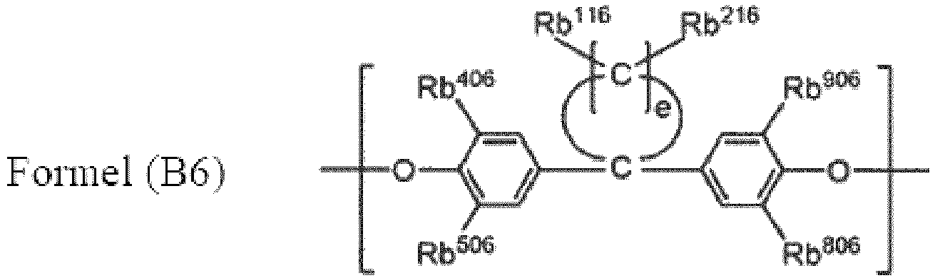

 in Formel (B1) Rb101 eine verzweigte Alkylgruppe mit 4 oder mehr und 20 oder weniger Kohlenstoffatomen darstellt, Rb201 ein Wasserstoffatom oder eine Alkylgruppe mit 1 oder mehr und 3 oder weniger Kohlenstoffatomen darstellt und Rb401, Rb501, Rb801 und Rb901 jeweils unabhängig voneinander ein Wasserstoffatom, eine Alkylgruppe mit 1 oder mehr und 4 oder weniger Kohlenstoffatomen, eine Alkoxygruppe mit 1 oder mehr und 6 oder weniger Kohlenstoffatomen oder ein Halogenatom darstellen,in Formel (B2) Rb102 eine lineare Alkylgruppe mit 4 oder mehr und 20 oder weniger Kohlenstoffatomen darstellt, Rb202 ein Wasserstoffatom oder eine Alkylgruppe mit 1 oder mehr und 3 oder weniger Kohlenstoffatomen darstellt und Rb402, Rb502, Rb802 und Rb902 jeweils unabhängig voneinander ein Wasserstoffatom, eine Alkylgruppe mit 1 oder mehr und 4 oder weniger Kohlenstoffatomen, eine Alkoxygruppe mit 1 oder mehr und 6 oder weniger Kohlenstoffatomen oder ein Halogenatom darstellen,in Formel (B3) Rb113 und Rb213 jeweils unabhängig voneinander ein Wasserstoffatom, eine lineare Alkylgruppe mit 1 oder mehr und 3 oder weniger Kohlenstoffatomen, eine Alkoxygruppe mit 1 oder mehr und 4 oder weniger Kohlenstoffatomen oder ein Halogenatom darstellen, d eine ganze Zahl von 7 oder größer und 15 oder kleiner darstellt und Rb403, Rb503, Rb803 und Rb903 jeweils unabhängig voneinander ein Wasserstoffatom, eine Alkylgruppe mit 1 oder mehr und 4 oder weniger Kohlenstoffatomen, eine Alkoxygruppe mit 1 oder mehr und 6 oder weniger Kohlenstoffatomen oder ein Halogenatom darstellen,in Formel (B4) Rb104 und Rb204 jeweils unabhängig voneinander ein Wasserstoffatom, eine Alkylgruppe mit 1 oder mehr und 3 oder weniger Kohlenstoffatomen darstellen und Rb404, Rb504, Rb804 und Rb904 jeweils unabhängig voneinander ein Wasserstoffatom, eine Alkylgruppe mit 1 oder mehr und 4 oder weniger Kohlenstoffatomen, eine Alkoxygruppe mit 1 oder mehr und 6 oder weniger Kohlenstoffatomen oder ein Halogenatom darstellen,in Formel (B5) Ar105 eine Arylgruppe mit 6 oder mehr und 12 oder weniger Kohlenstoffatomen oder eine Aralkylgruppe mit 7 oder mehr und 20 oder weniger Kohlenstoffatomen darstellt, Rb205 ein Wasserstoffatom oder eine Alkylgruppe mit 1 oder mehr und 3 oder weniger Kohlenstoffatomen darstellt und Rb405, Rb505, Rb805 und Rb905 jeweils unabhängig voneinander ein Wasserstoffatom, eine Alkylgruppe mit 1 oder mehr und 4 oder weniger Kohlenstoffatomen, eine Alkoxygruppe mit 1 oder mehr und 6 oder weniger Kohlenstoffatomen oder ein Halogenatom darstellen,in Formel (B6) Rb116 und Rb216 jeweils unabhängig voneinander ein Wasserstoffatom, eine lineare Alkylgruppe mit 1 oder mehr und 3 oder weniger Kohlenstoffatomen, eine Alkoxygruppe mit 1 oder mehr und 4 oder weniger Kohlenstoffatomen oder ein Halogenatom darstellen, e eine ganze Zahl von 4 oder größer und 6 oder kleiner darstellt und Rb406, Rb506, Rb806 und Rb906 jeweils unabhängig voneinander ein Wasserstoffatom, eine Alkylgruppe mit 1 oder mehr und 4 oder weniger Kohlenstoffatomen, eine Alkoxygruppe mit 1 oder mehr und 6 oder weniger Kohlenstoffatomen oder ein Halogenatom darstellen,in Formel (B7) Rb407, Rb507, Rb807 und Rb907 jeweils unabhängig voneinander ein Wasserstoffatom, eine Alkylgruppe mit 1 oder mehr und 4 oder weniger Kohlenstoffatomen, eine Alkoxygruppe mit 1 oder mehr und 6 oder weniger Kohlenstoffatomen oder ein Halogenatom darstellen,in Formel (B8) Rb408, Rb508, Rb808 und Rb908 jeweils unabhängig voneinander ein Wasserstoffatom, eine Alkylgruppe mit 1 oder mehr und 4 oder weniger Kohlenstoffatomen, eine Alkoxygruppe mit 1 oder mehr und 6 oder weniger Kohlenstoffatomen oder ein Halogenatom darstellen.
 - Elektrophotographischer Photorezeptor nach einem der Ansprüche 5 bis 7,
wobei das Polyarylatharz (1) die Dicarbonsäureeinheit (A) mit mindestens einer, die aus der Gruppe, die aus einer Dicarbonsäureeinheit (A2), die durch Formel (A2) dargestellt wird, und einer Dicarbonsäureeinheit (A4), die durch Formel (A4) dargestellt wird, besteht, ausgewählt wird, aufweist,
 in Formel (A2) n201 und n202 jeweils unabhängig voneinander eine ganze Zahl von 0 oder größer und 4 oder kleiner darstellen und n201 Stücke von Ra201 und n202 Stücke von Ra202 jeweils unabhängig voneinander eine Alkylgruppe mit 1 oder mehr und 10 oder weniger Kohlenstoffatomen, eine Arylgruppe mit 6 oder mehr und 12 oder weniger Kohlenstoffatomen oder eine Alkoxygruppe mit 1 oder mehr und 6 oder weniger Kohlenstoffatomen darstellen,in Formel (A4) n401 eine ganze Zahl von 0 oder größer und 6 oder kleiner darstellt und n401 Stücke von Ra401 jeweils unabhängig voneinander eine Alkylgruppe mit 1 oder mehr und 10 oder weniger Kohlenstoffatomen, eine Arylgruppe mit 6 oder mehr und 12 oder weniger Kohlenstoffatomen oder eine Alkoxygruppe mit 1 oder mehr und 6 oder weniger Kohlenstoffatomen darstellen.
 - Elektrophotographischer Photorezeptor nach einem der Ansprüche 5 bis 8,
wobei das Polyarylatharz (1) die Dioleinheit (B) mit mindestens einer Einheit, die aus der Gruppe, die aus einer Dioleinheit (B1), die durch Formel (B1) dargestellt wird, und einer Dioleinheit (B2), die durch Formel (B2) dargestellt wird, besteht, ausgewählt wird, aufweist,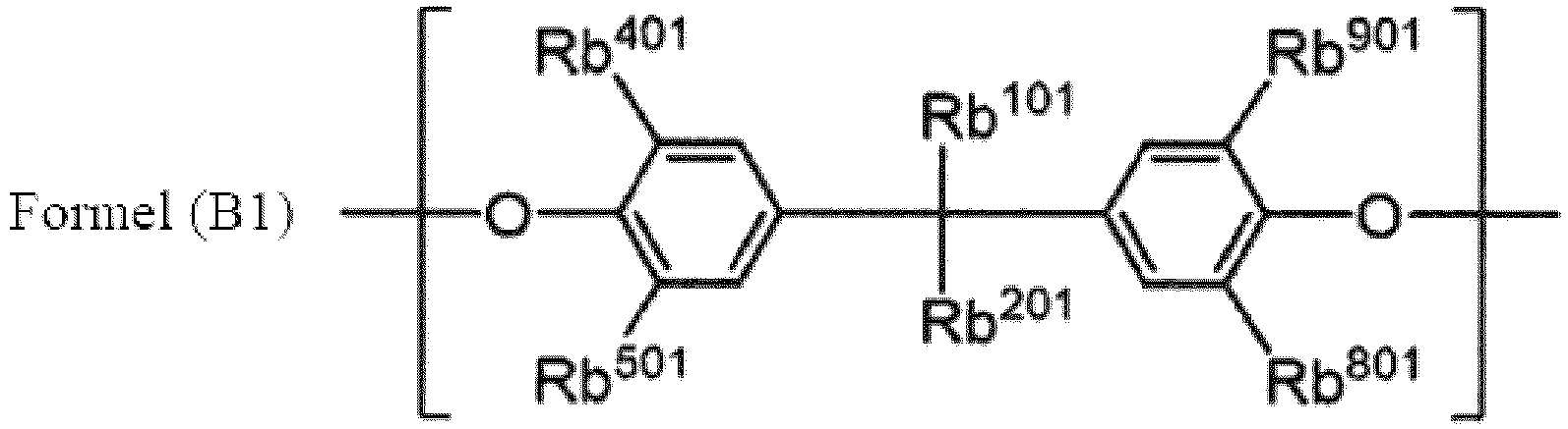
 in Formel (B1) Rb101 eine verzweigte Alkylgruppe mit 4 oder mehr und 20 oder weniger Kohlenstoffatomen darstellt, Rb201 ein Wasserstoffatom oder eine Alkylgruppe mit 1 oder mehr und 3 oder weniger Kohlenstoffatomen darstellt und Rb401, Rb501, Rb801 und Rb901 jeweils unabhängig voneinander ein Wasserstoffatom, eine Alkylgruppe mit 1 oder mehr und 4 oder weniger Kohlenstoffatomen, eine Alkoxygruppe mit 1 oder mehr und 6 oder weniger Kohlenstoffatomen oder ein Halogenatom darstellen,in Formel (B2) Rb102 eine lineare Alkylgruppe mit 4 oder mehr und 20 oder weniger Kohlenstoffatomen darstellt, Rb202 ein Wasserstoffatom oder eine Alkylgruppe mit 1 oder mehr und 3 oder weniger Kohlenstoffatomen darstellt und Rb402, Rb502, Rb802 und Rb902 jeweils unabhängig voneinander ein Wasserstoffatom, eine Alkylgruppe mit 1 oder mehr und 4 oder weniger Kohlenstoffatomen, eine Alkoxygruppe mit 1 oder mehr und 6 oder weniger Kohlenstoffatomen oder ein Halogenatom darstellen.
 - Prozesskartusche, umfassend:den elektrophotographischen Photorezeptor nach einem der Ansprüche 1 bis 9,wobei die Prozesskartusche an einer Bilderzeugungsvorrichtung anbringbar und von dieser lösbar ist.
- Bilderzeugungsvorrichtung, umfassend:den elektrophotographischen Photorezeptor nach einem der Ansprüche 1 bis 9;eine Ladevorrichtung, die eine Oberfläche des elektrophotographischen Photorezeptors lädt;eine Erzeugungsvorrichtung für elektrostatisches Latentbild, die ein elektrostatisches Latentbild auf der geladenen Oberfläche des elektrophotographischen Photorezeptors erzeugt;eine Entwicklungsvorrichtung, die das elektrostatische Latentbild, das auf der Oberfläche des elektrophotographischen Photorezeptors erzeugt wird, mit einem Entwickler, der einen Toner enthält, entwickelt, um ein Tonerbild zu erzeugen; undeine Übertragungsvorrichtung, die das Tonerbild auf eine Oberfläche eines Aufzeichnungsmediums überträgt.
Applications Claiming Priority (1)
| Application Number | Priority Date | Filing Date | Title |
|---|---|---|---|
| JP2023095896A JP2024176976A (ja) | 2023-06-09 | 2023-06-09 | 電子写真感光体、プロセスカートリッジ及び画像形成装置 |
Publications (2)
| Publication Number | Publication Date |
|---|---|
| EP4474913A1 EP4474913A1 (de) | 2024-12-11 |
| EP4474913B1 true EP4474913B1 (de) | 2025-07-09 |
Family
ID=89977289
Family Applications (1)
| Application Number | Title | Priority Date | Filing Date |
|---|---|---|---|
| EP24157753.5A Active EP4474913B1 (de) | 2023-06-09 | 2024-02-15 | Elektrophotographischer photorezeptor, prozesskartusche und bilderzeugungsvorrichtung |
Country Status (4)
| Country | Link |
|---|---|
| US (1) | US20240419091A1 (de) |
| EP (1) | EP4474913B1 (de) |
| JP (1) | JP2024176976A (de) |
| CN (1) | CN119105247A (de) |
Families Citing this family (1)
| Publication number | Priority date | Publication date | Assignee | Title |
|---|---|---|---|---|
| JP2026067493A (ja) | 2024-10-09 | 2026-04-21 | アルプスアルパイン株式会社 | オーディオ信号処理装置 |
Family Cites Families (15)
| Publication number | Priority date | Publication date | Assignee | Title |
|---|---|---|---|---|
| JP5910920B2 (ja) | 2011-11-04 | 2016-04-27 | 株式会社リコー | 電子写真感光体、プロセスカートリッジ及び画像形成装置 |
| JP2015078350A (ja) | 2013-09-12 | 2015-04-23 | 三菱化学株式会社 | ポリアリレート樹脂、及びそれを用いた電子写真感光体 |
| US9141006B2 (en) * | 2013-10-17 | 2015-09-22 | Xerox Corporation | Imaging member having improved imaging layers |
| JP6570223B2 (ja) | 2014-07-30 | 2019-09-04 | キヤノン株式会社 | 電子写真感光体、プロセスカートリッジおよび電子写真装置 |
| JP6921651B2 (ja) | 2017-06-29 | 2021-08-18 | キヤノン株式会社 | 電子写真感光体、プロセスカートリッジ及び電子写真装置 |
| JP6949619B2 (ja) | 2017-08-18 | 2021-10-13 | キヤノン株式会社 | 電子写真感光体、プロセスカートリッジ及び電子写真装置 |
| JP2019061146A (ja) * | 2017-09-27 | 2019-04-18 | 富士ゼロックス株式会社 | 電子写真感光体、プロセスカートリッジおよび画像形成装置 |
| JP7230818B2 (ja) | 2017-10-04 | 2023-03-01 | 三菱ケミカル株式会社 | 電子写真感光体、電子写真感光体カートリッジ及び画像形成装置 |
| JP7353824B2 (ja) | 2019-06-25 | 2023-10-02 | キヤノン株式会社 | 電子写真感光体、プロセスカートリッジおよび電子写真装置 |
| JP2021015223A (ja) | 2019-07-12 | 2021-02-12 | コニカミノルタ株式会社 | 電子写真感光体 |
| US11256185B2 (en) | 2019-10-29 | 2022-02-22 | Lexmark International, Inc. | Shaped charge generation layer for a photoconductive drum |
| JP7338402B2 (ja) | 2019-10-30 | 2023-09-05 | 京セラドキュメントソリューションズ株式会社 | 電子写真感光体 |
| JP2021117377A (ja) | 2020-01-27 | 2021-08-10 | キヤノン株式会社 | 電子写真感光体、プロセスカートリッジおよび電子写真装置 |
| JP7375633B2 (ja) | 2020-03-16 | 2023-11-08 | 京セラドキュメントソリューションズ株式会社 | 下引き層、下引き層の製造方法、電子写真感光体、及び画像形成装置 |
| US12613476B2 (en) * | 2021-09-24 | 2026-04-28 | Fujifilm Business Innovation Corp. | Electrophotographic photoreceptor, process cartridge, and image forming apparatus |
-
2023
- 2023-06-09 JP JP2023095896A patent/JP2024176976A/ja active Pending
-
2024
- 2024-02-15 EP EP24157753.5A patent/EP4474913B1/de active Active
- 2024-02-15 US US18/443,216 patent/US20240419091A1/en active Pending
- 2024-02-20 CN CN202410188155.6A patent/CN119105247A/zh active Pending
Also Published As
| Publication number | Publication date |
|---|---|
| EP4474913A1 (de) | 2024-12-11 |
| JP2024176976A (ja) | 2024-12-19 |
| CN119105247A (zh) | 2024-12-10 |
| US20240419091A1 (en) | 2024-12-19 |
Similar Documents
| Publication | Publication Date | Title |
|---|---|---|
| US20230266684A1 (en) | Image forming unit and image forming apparatus | |
| JP2024011918A (ja) | 電子写真感光体、プロセスカートリッジ及び画像形成装置 | |
| US12613476B2 (en) | Electrophotographic photoreceptor, process cartridge, and image forming apparatus | |
| JP2023047285A (ja) | 電子写真感光体、プロセスカートリッジ及び画像形成装置 | |
| JP2023130296A (ja) | 電子写真感光体、プロセスカートリッジ及び画像形成装置 | |
| EP4474913A1 (de) | Elektrophotographischer photorezeptor, prozesskartusche und bilderzeugungsvorrichtung | |
| EP4198632A1 (de) | Elektrophotographischer photorezeptor, prozesskartusche und bilderzeugungsvorrichtung | |
| JP7826734B2 (ja) | 電子写真感光体、プロセスカートリッジ及び画像形成装置 | |
| EP4478130B1 (de) | Elektrophotographischer photorezeptor, prozesskartusche und bilderzeugungsvorrichtung | |
| EP4603910A1 (de) | Elektrophotographischer photorezeptor, prozesskartusche und bilderzeugungsvorrichtung | |
| EP4741936A1 (de) | Elektrophotographischer photorezeptor, prozesskartusche und bilderzeugungsvorrichtung | |
| EP4603911A1 (de) | Elektrophotographischer photorezeptor, prozesskartusche und bilderzeugungsvorrichtung | |
| EP4592755A1 (de) | Elektrophotographischer photorezeptor, prozesskartusche und bilderzeugungsvorrichtung | |
| EP4741937A1 (de) | Elektrophotographischer photorezeptor, prozesskartusche und bilderzeugungsvorrichtung | |
| US20260133505A1 (en) | Electrophotographic photoreceptor, process cartridge, and image forming apparatus | |
| EP4741934A1 (de) | Elektrophotographischer photorezeptor, prozesskartusche und bilderzeugungsvorrichtung | |
| US20240053689A1 (en) | Electrophotographic photoreceptor, process cartridge, and image forming apparatus | |
| US20260133506A1 (en) | Electrophotographic photoreceptor, process cartridge, and image forming apparatus | |
| US20260133512A1 (en) | Electrophotographic photoreceptor, process cartridge, and image forming apparatus | |
| EP4530724A1 (de) | Elektrophotographischer photorezeptor, prozesskartusche und bilderzeugungsvorrichtung | |
| EP4575646A1 (de) | Elektrophotographischer photorezeptor, prozesskartusche und bilderzeugungsvorrichtung | |
| US20250102929A1 (en) | Electrophotographic photoreceptor, process cartridge, and image forming apparatus | |
| US20230280668A1 (en) | Electrophotographic photoreceptor, process cartridge, and image forming apparatus | |
| EP4741933A1 (de) | Elektrophotographischer photorezeptor, prozesskartusche und bilderzeugungsvorrichtung | |
| US20260133511A1 (en) | Electrophotographic photoreceptor, process cartridge, and image forming apparatus |
Legal Events
| Date | Code | Title | Description |
|---|---|---|---|
| PUAI | Public reference made under article 153(3) epc to a published international application that has entered the european phase |
Free format text: ORIGINAL CODE: 0009012 |
|
| STAA | Information on the status of an ep patent application or granted ep patent |
Free format text: STATUS: THE APPLICATION HAS BEEN PUBLISHED |
|
| AK | Designated contracting states |
Kind code of ref document: A1 Designated state(s): AL AT BE BG CH CY CZ DE DK EE ES FI FR GB GR HR HU IE IS IT LI LT LU LV MC ME MK MT NL NO PL PT RO RS SE SI SK SM TR |
|
| STAA | Information on the status of an ep patent application or granted ep patent |
Free format text: STATUS: REQUEST FOR EXAMINATION WAS MADE |
|
| 17P | Request for examination filed |
Effective date: 20250122 |
|
| GRAP | Despatch of communication of intention to grant a patent |
Free format text: ORIGINAL CODE: EPIDOSNIGR1 |
|
| STAA | Information on the status of an ep patent application or granted ep patent |
Free format text: STATUS: GRANT OF PATENT IS INTENDED |
|
| INTG | Intention to grant announced |
Effective date: 20250411 |
|
| GRAS | Grant fee paid |
Free format text: ORIGINAL CODE: EPIDOSNIGR3 |
|
| GRAA | (expected) grant |
Free format text: ORIGINAL CODE: 0009210 |
|
| STAA | Information on the status of an ep patent application or granted ep patent |
Free format text: STATUS: THE PATENT HAS BEEN GRANTED |
|
| AK | Designated contracting states |
Kind code of ref document: B1 Designated state(s): AL AT BE BG CH CY CZ DE DK EE ES FI FR GB GR HR HU IE IS IT LI LT LU LV MC ME MK MT NL NO PL PT RO RS SE SI SK SM TR |
|
| REG | Reference to a national code |
Ref country code: GB Ref legal event code: FG4D |
|
| REG | Reference to a national code |
Ref country code: CH Ref legal event code: EP |
|
| REG | Reference to a national code |
Ref country code: IE Ref legal event code: FG4D |
|
| REG | Reference to a national code |
Ref country code: DE Ref legal event code: R096 Ref document number: 602024000281 Country of ref document: DE |
|
| REG | Reference to a national code |
Ref country code: NL Ref legal event code: MP Effective date: 20250709 |
|
| PG25 | Lapsed in a contracting state [announced via postgrant information from national office to epo] |
Ref country code: PT Free format text: LAPSE BECAUSE OF FAILURE TO SUBMIT A TRANSLATION OF THE DESCRIPTION OR TO PAY THE FEE WITHIN THE PRESCRIBED TIME-LIMIT Effective date: 20251110 |
|
| PG25 | Lapsed in a contracting state [announced via postgrant information from national office to epo] |
Ref country code: NL Free format text: LAPSE BECAUSE OF FAILURE TO SUBMIT A TRANSLATION OF THE DESCRIPTION OR TO PAY THE FEE WITHIN THE PRESCRIBED TIME-LIMIT Effective date: 20250709 |
|
| REG | Reference to a national code |
Ref country code: AT Ref legal event code: MK05 Ref document number: 1812374 Country of ref document: AT Kind code of ref document: T Effective date: 20250709 |
|
| PG25 | Lapsed in a contracting state [announced via postgrant information from national office to epo] |
Ref country code: IS Free format text: LAPSE BECAUSE OF FAILURE TO SUBMIT A TRANSLATION OF THE DESCRIPTION OR TO PAY THE FEE WITHIN THE PRESCRIBED TIME-LIMIT Effective date: 20251109 |
|
| PG25 | Lapsed in a contracting state [announced via postgrant information from national office to epo] |
Ref country code: NO Free format text: LAPSE BECAUSE OF FAILURE TO SUBMIT A TRANSLATION OF THE DESCRIPTION OR TO PAY THE FEE WITHIN THE PRESCRIBED TIME-LIMIT Effective date: 20251009 |
|
| REG | Reference to a national code |
Ref country code: LT Ref legal event code: MG9D |
|
| PG25 | Lapsed in a contracting state [announced via postgrant information from national office to epo] |
Ref country code: AT Free format text: LAPSE BECAUSE OF FAILURE TO SUBMIT A TRANSLATION OF THE DESCRIPTION OR TO PAY THE FEE WITHIN THE PRESCRIBED TIME-LIMIT Effective date: 20250709 |
|
| PG25 | Lapsed in a contracting state [announced via postgrant information from national office to epo] |
Ref country code: FI Free format text: LAPSE BECAUSE OF FAILURE TO SUBMIT A TRANSLATION OF THE DESCRIPTION OR TO PAY THE FEE WITHIN THE PRESCRIBED TIME-LIMIT Effective date: 20250709 |
|
| PG25 | Lapsed in a contracting state [announced via postgrant information from national office to epo] |
Ref country code: HR Free format text: LAPSE BECAUSE OF FAILURE TO SUBMIT A TRANSLATION OF THE DESCRIPTION OR TO PAY THE FEE WITHIN THE PRESCRIBED TIME-LIMIT Effective date: 20250709 |
|
| PGFP | Annual fee paid to national office [announced via postgrant information from national office to epo] |
Ref country code: FR Payment date: 20251231 Year of fee payment: 3 |
|
| PG25 | Lapsed in a contracting state [announced via postgrant information from national office to epo] |
Ref country code: GR Free format text: LAPSE BECAUSE OF FAILURE TO SUBMIT A TRANSLATION OF THE DESCRIPTION OR TO PAY THE FEE WITHIN THE PRESCRIBED TIME-LIMIT Effective date: 20251010 |
|
| PG25 | Lapsed in a contracting state [announced via postgrant information from national office to epo] |
Ref country code: SE Free format text: LAPSE BECAUSE OF FAILURE TO SUBMIT A TRANSLATION OF THE DESCRIPTION OR TO PAY THE FEE WITHIN THE PRESCRIBED TIME-LIMIT Effective date: 20250709 |
|
| PG25 | Lapsed in a contracting state [announced via postgrant information from national office to epo] |
Ref country code: LV Free format text: LAPSE BECAUSE OF FAILURE TO SUBMIT A TRANSLATION OF THE DESCRIPTION OR TO PAY THE FEE WITHIN THE PRESCRIBED TIME-LIMIT Effective date: 20250709 |
|
| PG25 | Lapsed in a contracting state [announced via postgrant information from national office to epo] |
Ref country code: PL Free format text: LAPSE BECAUSE OF FAILURE TO SUBMIT A TRANSLATION OF THE DESCRIPTION OR TO PAY THE FEE WITHIN THE PRESCRIBED TIME-LIMIT Effective date: 20250709 Ref country code: BG Free format text: LAPSE BECAUSE OF FAILURE TO SUBMIT A TRANSLATION OF THE DESCRIPTION OR TO PAY THE FEE WITHIN THE PRESCRIBED TIME-LIMIT Effective date: 20250709 |
|
| PG25 | Lapsed in a contracting state [announced via postgrant information from national office to epo] |
Ref country code: RS Free format text: LAPSE BECAUSE OF FAILURE TO SUBMIT A TRANSLATION OF THE DESCRIPTION OR TO PAY THE FEE WITHIN THE PRESCRIBED TIME-LIMIT Effective date: 20251009 |
|
| PG25 | Lapsed in a contracting state [announced via postgrant information from national office to epo] |
Ref country code: ES Free format text: LAPSE BECAUSE OF FAILURE TO SUBMIT A TRANSLATION OF THE DESCRIPTION OR TO PAY THE FEE WITHIN THE PRESCRIBED TIME-LIMIT Effective date: 20250709 |
|
| P01 | Opt-out of the competence of the unified patent court (upc) registered |
Free format text: CASE NUMBER: UPC_APP_0000827_4474913/2026 Effective date: 20260109 |
|
| PG25 | Lapsed in a contracting state [announced via postgrant information from national office to epo] |
Ref country code: SM Free format text: LAPSE BECAUSE OF FAILURE TO SUBMIT A TRANSLATION OF THE DESCRIPTION OR TO PAY THE FEE WITHIN THE PRESCRIBED TIME-LIMIT Effective date: 20250709 |
|
| PG25 | Lapsed in a contracting state [announced via postgrant information from national office to epo] |
Ref country code: DK Free format text: LAPSE BECAUSE OF FAILURE TO SUBMIT A TRANSLATION OF THE DESCRIPTION OR TO PAY THE FEE WITHIN THE PRESCRIBED TIME-LIMIT Effective date: 20250709 |
|
| PGFP | Annual fee paid to national office [announced via postgrant information from national office to epo] |
Ref country code: DE Payment date: 20251230 Year of fee payment: 3 |
|
| PG25 | Lapsed in a contracting state [announced via postgrant information from national office to epo] |
Ref country code: IT Free format text: LAPSE BECAUSE OF FAILURE TO SUBMIT A TRANSLATION OF THE DESCRIPTION OR TO PAY THE FEE WITHIN THE PRESCRIBED TIME-LIMIT Effective date: 20250709 |
|
| PG25 | Lapsed in a contracting state [announced via postgrant information from national office to epo] |
Ref country code: CZ Free format text: LAPSE BECAUSE OF FAILURE TO SUBMIT A TRANSLATION OF THE DESCRIPTION OR TO PAY THE FEE WITHIN THE PRESCRIBED TIME-LIMIT Effective date: 20250709 |
|
| PG25 | Lapsed in a contracting state [announced via postgrant information from national office to epo] |
Ref country code: SK Free format text: LAPSE BECAUSE OF FAILURE TO SUBMIT A TRANSLATION OF THE DESCRIPTION OR TO PAY THE FEE WITHIN THE PRESCRIBED TIME-LIMIT Effective date: 20250709 Ref country code: EE Free format text: LAPSE BECAUSE OF FAILURE TO SUBMIT A TRANSLATION OF THE DESCRIPTION OR TO PAY THE FEE WITHIN THE PRESCRIBED TIME-LIMIT Effective date: 20250709 |
|
| PLBE | No opposition filed within time limit |
Free format text: ORIGINAL CODE: 0009261 |
|
| STAA | Information on the status of an ep patent application or granted ep patent |
Free format text: STATUS: NO OPPOSITION FILED WITHIN TIME LIMIT |