EP4471850A1 - Strukturierung von halbleitervorrichtungen - Google Patents
Strukturierung von halbleitervorrichtungen Download PDFInfo
- Publication number
- EP4471850A1 EP4471850A1 EP23176197.4A EP23176197A EP4471850A1 EP 4471850 A1 EP4471850 A1 EP 4471850A1 EP 23176197 A EP23176197 A EP 23176197A EP 4471850 A1 EP4471850 A1 EP 4471850A1
- Authority
- EP
- European Patent Office
- Prior art keywords
- layer
- edge area
- mask
- top surface
- semiconductor device
- Prior art date
- Legal status (The legal status is an assumption and is not a legal conclusion. Google has not performed a legal analysis and makes no representation as to the accuracy of the status listed.)
- Pending
Links
Images



Classifications
-
- G—PHYSICS
- G03—PHOTOGRAPHY; CINEMATOGRAPHY; ANALOGOUS TECHNIQUES USING WAVES OTHER THAN OPTICAL WAVES; ELECTROGRAPHY; HOLOGRAPHY
- G03F—PHOTOMECHANICAL PRODUCTION OF TEXTURED OR PATTERNED SURFACES, e.g. FOR PRINTING, FOR PROCESSING OF SEMICONDUCTOR DEVICES; MATERIALS THEREFOR; ORIGINALS THEREFOR; APPARATUS SPECIALLY ADAPTED THEREFOR
- G03F7/00—Photomechanical, e.g. photolithographic, production of textured or patterned surfaces, e.g. printing surfaces; Materials therefor, e.g. comprising photoresists; Apparatus specially adapted therefor
- G03F7/0002—Lithographic processes using patterning methods other than those involving the exposure to radiation, e.g. by stamping
-
- H—ELECTRICITY
- H10—SEMICONDUCTOR DEVICES; ELECTRIC SOLID-STATE DEVICES NOT OTHERWISE PROVIDED FOR
- H10W—GENERIC PACKAGES, INTERCONNECTIONS, CONNECTORS OR OTHER CONSTRUCTIONAL DETAILS OF DEVICES COVERED BY CLASS H10
- H10W72/00—Interconnections or connectors in packages
- H10W72/01—Manufacture or treatment
- H10W72/019—Manufacture or treatment of bond pads
-
- G—PHYSICS
- G03—PHOTOGRAPHY; CINEMATOGRAPHY; ANALOGOUS TECHNIQUES USING WAVES OTHER THAN OPTICAL WAVES; ELECTROGRAPHY; HOLOGRAPHY
- G03F—PHOTOMECHANICAL PRODUCTION OF TEXTURED OR PATTERNED SURFACES, e.g. FOR PRINTING, FOR PROCESSING OF SEMICONDUCTOR DEVICES; MATERIALS THEREFOR; ORIGINALS THEREFOR; APPARATUS SPECIALLY ADAPTED THEREFOR
- G03F7/00—Photomechanical, e.g. photolithographic, production of textured or patterned surfaces, e.g. printing surfaces; Materials therefor, e.g. comprising photoresists; Apparatus specially adapted therefor
- G03F7/0035—Multiple processes, e.g. applying a further resist layer on an already in a previously step, processed pattern or textured surface
-
- H—ELECTRICITY
- H10—SEMICONDUCTOR DEVICES; ELECTRIC SOLID-STATE DEVICES NOT OTHERWISE PROVIDED FOR
- H10P—GENERIC PROCESSES OR APPARATUS FOR THE MANUFACTURE OR TREATMENT OF DEVICES COVERED BY CLASS H10
- H10P76/00—Manufacture or treatment of masks on semiconductor bodies, e.g. by lithography or photolithography
- H10P76/20—Manufacture or treatment of masks on semiconductor bodies, e.g. by lithography or photolithography of masks comprising organic materials
- H10P76/204—Manufacture or treatment of masks on semiconductor bodies, e.g. by lithography or photolithography of masks comprising organic materials of organic photoresist masks
- H10P76/2041—Photolithographic processes
-
- H—ELECTRICITY
- H10—SEMICONDUCTOR DEVICES; ELECTRIC SOLID-STATE DEVICES NOT OTHERWISE PROVIDED FOR
- H10P—GENERIC PROCESSES OR APPARATUS FOR THE MANUFACTURE OR TREATMENT OF DEVICES COVERED BY CLASS H10
- H10P76/00—Manufacture or treatment of masks on semiconductor bodies, e.g. by lithography or photolithography
- H10P76/40—Manufacture or treatment of masks on semiconductor bodies, e.g. by lithography or photolithography of masks comprising inorganic materials
- H10P76/408—Manufacture or treatment of masks on semiconductor bodies, e.g. by lithography or photolithography of masks comprising inorganic materials characterised by their sizes, orientations, dispositions, behaviours or shapes
- H10P76/4085—Manufacture or treatment of masks on semiconductor bodies, e.g. by lithography or photolithography of masks comprising inorganic materials characterised by their sizes, orientations, dispositions, behaviours or shapes characterised by the processes involved to create the masks
-
- H—ELECTRICITY
- H10—SEMICONDUCTOR DEVICES; ELECTRIC SOLID-STATE DEVICES NOT OTHERWISE PROVIDED FOR
- H10W—GENERIC PACKAGES, INTERCONNECTIONS, CONNECTORS OR OTHER CONSTRUCTIONAL DETAILS OF DEVICES COVERED BY CLASS H10
- H10W70/00—Package substrates; Interposers; Redistribution layers [RDL]
- H10W70/60—Insulating or insulated package substrates; Interposers; Redistribution layers
- H10W70/62—Insulating or insulated package substrates; Interposers; Redistribution layers characterised by their interconnections
- H10W70/65—Shapes or dispositions of interconnections
-
- H—ELECTRICITY
- H10—SEMICONDUCTOR DEVICES; ELECTRIC SOLID-STATE DEVICES NOT OTHERWISE PROVIDED FOR
- H10W—GENERIC PACKAGES, INTERCONNECTIONS, CONNECTORS OR OTHER CONSTRUCTIONAL DETAILS OF DEVICES COVERED BY CLASS H10
- H10W90/00—Package configurations
- H10W90/701—Package configurations characterised by the relative positions of pads or connectors relative to package parts
-
- H—ELECTRICITY
- H10—SEMICONDUCTOR DEVICES; ELECTRIC SOLID-STATE DEVICES NOT OTHERWISE PROVIDED FOR
- H10W—GENERIC PACKAGES, INTERCONNECTIONS, CONNECTORS OR OTHER CONSTRUCTIONAL DETAILS OF DEVICES COVERED BY CLASS H10
- H10W70/00—Package substrates; Interposers; Redistribution layers [RDL]
- H10W70/01—Manufacture or treatment
- H10W70/05—Manufacture or treatment of insulating or insulated package substrates, or of interposers, or of redistribution layers
-
- H—ELECTRICITY
- H10—SEMICONDUCTOR DEVICES; ELECTRIC SOLID-STATE DEVICES NOT OTHERWISE PROVIDED FOR
- H10W—GENERIC PACKAGES, INTERCONNECTIONS, CONNECTORS OR OTHER CONSTRUCTIONAL DETAILS OF DEVICES COVERED BY CLASS H10
- H10W72/00—Interconnections or connectors in packages
- H10W72/90—Bond pads, in general
- H10W72/921—Structures or relative sizes of bond pads
- H10W72/922—Bond pads being integral with underlying chip-level interconnections
-
- H—ELECTRICITY
- H10—SEMICONDUCTOR DEVICES; ELECTRIC SOLID-STATE DEVICES NOT OTHERWISE PROVIDED FOR
- H10W—GENERIC PACKAGES, INTERCONNECTIONS, CONNECTORS OR OTHER CONSTRUCTIONAL DETAILS OF DEVICES COVERED BY CLASS H10
- H10W72/00—Interconnections or connectors in packages
- H10W72/90—Bond pads, in general
- H10W72/931—Shapes of bond pads
- H10W72/934—Cross-sectional shape, i.e. in side view
Definitions
- the present invention relates to a method of manufacturing a semiconductor device.
- 'MOSFET' Metal Oxide Semiconductor Field Effect Transistor
- the thickness of the metallisation layer is guided by bond-force considerations for wire-bonded devices, or by some aspect of spreading resistance for clip-bonded devices.
- the metallisation layer should be as thick as possible, for the device to exhibit both low on-resistance, Rds(on), and uniform current spreading.
- a thick metallisation layer is desirable electrically, it is sub-optimal in mechanical terms, because semiconductor devices are typically manufactured with a passivation layer such as Si 3 N 4 , SiO 2 or a combination thereof, to protect the device from environmental contamination and surface damage, but which is prone to cracking out of thermal or temperature cycling ('TMCL') reliability test, particularly in edge areas.
- a passivation layer such as Si 3 N 4 , SiO 2 or a combination thereof
- Semiconductor devices are accordingly manufactured mostly using a single metal layer, the thickness of which is optimised for either low Rds(on) or for mechanical robustness with a thin layer and, more rarely, with dual-layer metallisation techniques as a compromise to try and satisfy both requirements.
- dual-layer metallisation typically requires at least two additional lithography layers, to accommodate both the second metal layer and the contact formation, together with some form of chemical mechanical planarization (CMP) processing in order to maintain the topography as flat as possible, for mitigating cracking.
- CMP chemical mechanical planarization
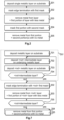
- a method of manufacturing a semiconductor device comprises steps of depositing a layer of metallic material onto a substrate, the layer having a top surface ; masking at least an edge area of the layer with a first lithography mask ; removing metal material from the edge area according to the first mask, whereby a first portion of the edge area has a thickness intermediate the substrate and the layer top surface ; masking the first portion of the edge area with a second lithography mask; and removing metal material from the first portion according to the second mask, whereby at least a second portion of the edge area is free of deposited metallic material.
- areas of semiconductor devices requiring low resistance such as their active area
- areas of semiconductor devices sensitive to topography such as their edge termination
- areas of semiconductor devices sensitive to topography such as their edge termination
- reduced metallisation thickness wherein the reduction in metallisation thickness reduction is achieved with just one photolithography mask and a wet or dry removal, e.g. by etching.
- the solution disclosed thus advantageously reduces the number of lithography masks required to deliver both a thick layer in the active area and a thinner layer in the adjacent edge area of a semiconductor device such as a power MOSFET, which usefully combines characteristics of low Rds(on) and mechanical robustness.
- Certain embodiments of the method may comprise the further step of configuring the second mask to define at least one member in the first portion, delimited by adjacent second portions.
- the member so defined is advantageous for certain types of semiconductor devices requiring at least one gate member in the edge termination area, such as MOSFETs.
- the configuration of the second mask may further comprise defining a second member in the first portion.
- the second member so defined is advantageous for certain types of semiconductor devices requiring at least one gate member and at least one source member in the edge termination area, with the gate member located intermediate the source member and the layer adjacent the first portion.
- Certain embodiments of the method may comprise the further step of configuring the first mask to define the or each member with a first width, wherein the configuration of the second mask further comprising defining at least one of the or each member with a second width larger than the first width.
- the selective etching proposed in this embodiment can provide, in the context of any edge area configured with at least one gate member, a gate busbar which retains its full metal thickness, identical to the thickness of the active area of the device, and which minimises the impact of a thinner metallisation layer on the gate resistance R G of the device.
- the selective etching proposed in this embodiment can also provide, in the context of any edge area configured with gate and source members, both a gate busbar and a source busbar which contribute to reducing passivation cracks and pattern shift, as both retain thicker metal at their centre for best conductivity, while keeping thinner metal around the periphery of the structure where thermomechanical stress is high. This results in minimal impact on the gate resistance R G , while improving mechanical robustness of the device significantly.
- the step of depositing may further comprise interleaving at least one layer of a second material intermediate the substrate and the layer top surface, the interleaved layer having a respective top surface; and the step of removing metal material from the edge area may further comprises removing metal material, whereby the first portion has a thickness intermediate the substrate and the interleaved layer top surface.
- the interleaved layer in such embodiments constitutes a mid-layer end-point detection barrier, located intermediate the active area and the edge area.
- the step of depositing may further comprise interleaving a plurality of layers of a second material intermediate the substrate and the layer top surface, each interleaved layer having a respective top surface; the method comprising the further step of configuring a plurality of first masks in a sequence for staggering the edge area at each of the plurality of interleaved layers; and the step of removing metal material from the edge area further comprises removing metal material with each of the plurality of the first masks.
- the step of configuring a plurality of first masks may further comprise configuring at least the last first mask in the sequence to define the at least two members in the first portion.
- the manufacturing sequence may thus include thinning the member(s), e.g. the gate member or the gate and source busbars, down in the first one, two or more etches, in order to reduce thermomechanical stress, but preserving metallisation thickness in the following one or two etches, in order to maintain a low R G .
- the second material for interleaved layer(s) may be selected from a first group comprising Titanium, Vanadium, Chromium, Zirconium, Niobium, Molybdenum, Hafnium, Tantalum, Tungsten; or from a second group comprising Cobalt, Nickel, Copper, Rhodium, Palladium, Silver, Iridium, Platinum, Gold; or from a group comprising alloys of the first and/or second group.
- the method may comprise the further step of reacting the second material with oxygen (O 2 ) or with nitrogen (N 2 ).
- the semiconductor device 10 comprises, in cross-section, a substrate 12 optionally covered by an inter-layer-dielectric ( ⁇ ILD') layer 14, onto a top surface of which a single metallic layer 16 is deposited, typically of aluminum copper (AlCu), in a particular thickness of e.g. 3 ⁇ m.
- ⁇ ILD' inter-layer-dielectric
- the deposition may be performed with any technique known to the skilled reader, for example a physical vapour deposition ( ⁇ PVD') technique that is well-known in the particular field of semiconductor manufacturing, implemented as either sputtering or evaporation.
- a photolithography process as described in the next paragraph is optionally applied to the metallic layer 16, then a passivation layer 18 such as Si3N4, SiO2 or a combination thereof is applied to the top surface of the device 10.
- the gate and source members 32, 34 are typically formed by masking the metallic layer 16 with a photolithography mask encoding the respective locations of the gate and source members 32, 34 relative to the active area 20, then performing a wet or dry etching operation to remove metallic material from the layer 16 down to the ILD layer 14 according to the mask, accordingly wherein interstitial portions 40 of the metallic layer 16 are fully removed in the edge area 30, respectively between the edge of the active area 20 and the gate member 32, between the gate and source members themselves, and from the source member 34 to the edge of the substrate 12. Accordingly both the active area 20 and the gate and source members 32, 34 of the prior art semiconductor device 10 exhibit a same thickness, i.e. vertical height relative to the surface of the substrate and ILD layers 12, 14.
- the higher incidence of passivation cracking has been attributed to a phenomenon known as the 'yield strength' of the material, wherein it begins to deform plastically, causing the material to detach or delaminate itself from its neighbouring materials, and accordingly bear thermomechanical stresses in the device alone.
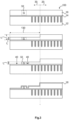
- the semiconductor device 100 of Figure 1B comprises, in cross-section, the same substrate 12 optionally covered by an ILD layer 14, onto a top surface of which a single metallic layer 16 is deposited at step 201, for example by sputterring a metal alloy in a thickness t 1 of 3 ⁇ m again.
- a photolithography process according to the method of the invention as described hereinafter with reference to Figure 2 and illustrated in Figure 3 for the semiconductor device 100 of Figure 1B , is then applied to the metallic layer 16, then a passivation layer 18 such as Si3N4, SiO2 or a combination thereof is again applied to the top surface of the device 100.
- FIG. 1B The detail shown in Figure 1B is again a lateral edge region of the device 100, wherein the active area 20 is still delimited by an edge area 30, or edge termination area, in the example comprising a single gate member 32.
- the edge area 30 of the metallic layer 16 is masked with a first lithography mask at step 202.
- a thickness of metallic material is then removed from the edge area according to the first mask, for instance with a dry or wet etching process, whereby a first portion 130 of the edge area has a remaining thickness t 2 intermediate the substrate 12 (optionally covered by the ILD layer 14) and the top surface of the metallic layer 16, i.e. less than the thickness t 1 of 3 ⁇ m of the metallic layer 16 deposited at step 201, for example 1 or 2 ⁇ m.
- the first portion 130 extends from the edge of the active area 20 immediately adjacent the edge area 30, i.e. the location at which the metallic layer 16 transitions from its full thickness t 1 to the reduced thickness t 2 and effectively forms a step, toward the device's lateral edge.
- the first portion 130 may have a length in the range 20 to 50 ⁇ m.
- the topography of the edge area 30 in this first example device 100 is then formed by masking the first portion 130 of the edge area with a second lithography mask at step 203, then removing material from the metallic layer 16 in the first portion 130 over the remaining thickness t 2 , i.e. down to the top surface of the substrate layer 12 (or ILD layer 14 when present) according to the second mask at step 204, accordingly wherein one or more second portions 40 of the metallic layer 16 in the edge area 30 are fully removed.
- a second portion 40 is located between a certain distance from the step at the edge of the active area 20 and a side of the gate member 32 facing the active area 20, and a further second portion is located from the opposed side of the gate member 34 to the edge of the substrate 12.
- the active area 20 maintains its original thickness t 1 of deposited metallic layer 16 and is thus optimised for a reduced Rds(on). This region will typically be inside the active area of the device 100 and will extend approximately up to the edge of the edge termination structure.
- the edge area 30, including the gate member 32 in this example, is advantageously configured with a thinner thickness t 2 , and accordingly optimised for metallic yield strength.
- the step intermediate the active and edge areas 20, 30 may still be prone to passivation cracking.
- the tensile energy will be released at the foot of the step, wherein any resulting propagating cracks will disperse over the edge area 30 which, given its length of 20 to 50 ⁇ m, will absorb even the longest of cracks seen in practice.
- Inter-areas propagating cracks are considered benign because they are transmitted between parts of the same metal structure 16 without penetration to underlying layers.
- Semiconductor devices manufactured with the present method are accordingly exceedingly robust against passivation cracks and uncontrolled thermomechanical energy release.
- the method of the invention may be practiced without configuring the edge area 30, without any other topography than the edge of the first portion 130 most distal the active area 20, i.e. the location at which the metallic layer 16 transitions from its reduced thickness t 2 down to the top surface of the substrate layer 12 (or ILD layer 14 when present), thus wherein a single second portion 40 of the edge area 30 most distal the active area 20 is free of deposited metallic material after step 204.
- the edge area 30 was configured with a single gate member 32.
- the edge area 30 of the semiconductor device 400 is configured with two members, respectively a gate member 32 and a source member 34.
- the metallic layer 16 is deposited at step 201, the first mask is applied at step 202 and material is removed from the metallic layer 16 according to the first mask at step 203 as previously described.
- the second mask of step 204 is further configured to define the second source member 34 in addition to the first gate member 32 whereby, after applying the second mask to the first portion 130 at step 204 and removing material therefrom removed over the remaining thickness t 2 according to the second mask at step 205, a second portion 40 is located between a certain distance from the step at the edge of the active area 20 and a side of the gate member 32 facing the active area 20, a further second portion is located from the opposed side of the gate member 32 and a side of the source member 34 facing the active area 20, and another second portion is located from the opposed side of the source member 34 to the edge of the substrate 12.
- the edge area 30, including both gate and source members 32, 34 in this example, is again advantageously configured with a thinner thickness t 2 , and thus optimised for metallic yield strength.
- the edge area 30 of the semiconductor device 500 is again configured with a gate member 32 and a source member 34.
- the gate member 32 is designed as a busbar for enhancing the gate resistance property R G of the secomiconductor device 500, and preferably retains the full thickness t 1 of the metallic layer 16 as deposited at step 201 for this purpose.
- the first mask of step 202 is additionally configured to define an upper portion of the gate member 32 with a first width w 1 and the second mask of step 204 is additionally configured to both define the second source member 34 and to define a lower portion of the gate member 34 with a second width w 2 larger than w 1 , noting that the second source member 34 may be configured with the same larger width w 2 .
- the metallic layer 16 is deposited at step 201, the first mask is applied at step 202 and material is removed from the metallic layer 16 according to the first mask at step 203, thus on either side of the upper portion of the gate member 32 with a first width w 1 .
- the second mask is applied at step 204 and material is removed over the remaining thickness t 2 in the first portion 130 according to the second mask at step 205, thus wherein a second portion 40 is located respectively on a side of the lower portion of the gate member 32 with a larger width w 2 , centrally of the opposed side of the lower portion of the gate member 32 and a side of the source member 34, and on the opposed side of the source member 34.
- the edge area 30 of the semiconductor device 600 is again configured with a gate member 32 and a source member 34 wherein, in this embodiment, both members are designed as busbars, each the full thickness t 1 of the metallic layer 16 as deposited at step 201.
- the first mask of step 202 is additionally configured to define an upper portion of both the gate and source members 32, 34 with the first width w 1 and the second mask of step 204 is additionally configured to both define a lower portion of each of the gate and source members 32, 34 with the second width w 2 larger than w 1 .
- the metallic layer 16 is deposited at step 201, the first mask is applied at step 202 and material is removed from the metallic layer 16 according to the first mask at step 203, thus on either side of the respective upper portion of each of the gate and source members 32, 34.
- the second mask is applied at step 204 and material is removed over the remaining thickness t 2 in the first portion 130 according to the second mask at step 205, whereby second portions 40 are located as previously described with reference to Figure 5 .
- the edge area 30, including both gate and source members 32, 34 is still advantageously configured, at least partially in this embodiment, with a thinner thickness t 2 , and thus optimised for metallic yield strength, and each of the gate and source members 32 has both a full thickness t 1 and a wider lower portion providing thicker metal at its centre, resulting in a device 600 combining enhanced conductivity and improved mechanical robustness, as the wider lower portion of each busbar 32, 34 enables pattern shift and passivation cracks to be minimised in the edge area 30.
- the method step of deposition 201 in such variants comprises a series of sub-steps, including at least a first sub-step 701 of depositing an initial sub-layer 810 of metallic material onto the substrate 12 (or ILD layer 14 atop same), in a thickness t 3 that is a fraction of the full thickness t 1 of metallisation desired for the active area 20, and which may correspond to the reduced thickness t 2 described in previous embodiments, in the example case of a single interleaved layer.
- At least one instance of a next sub-step 702 involves depositing the, or the first, interleaving layer 820 of second material, in the example titanium (Ti) or a titanium nitride (TiN) alloy, in as minimal a thickness as permitted by the depositing technique used.
- At least one instance of a next sub-step 703 involves depositing a next sub-layer 810 of metallic material onto the deposited layer of second material 820, in substantially the same thickness t 3 as the initial sub-layer, or another.
- the method returns to sub-step 702, wherein a further interleaving layer 820 of second material is deposited, whence the next sub-layer 810 of metallic material gets deposited onto the second-deposited layer of second material 820 at step 703, and so on and so forth.
- the last-deposited sub-layer 810 of metallic material achieves the full thickness t 1 of metallisation desired for the active area 20 and the question of sub-step 704 is answered negatively, wherein the layer 16 comprises one or more interleaved layers 820 of second material.
- Control proceeds to the masking of step 202 with a first lithography mask as previously described, then the removal of material from the metallic layer 16 in the edge area 30 according to same at step 203.
- the masking and removal of steps 202, 2023 may either include or exclude the interleaving layer 820 underlying the volume of metallic material removed.
- the interleaving layer 820 is maintained uniformly within the first portion 130, including atop the gate and source members 32, 34 of reduced thickness t 2 , accordingly the first portion has a thickness intermediate the substrate and the interleaved layer top surface.
- the interleaving layer 820 is maintained atop gate and source members 32, 34 but not in other aspects of the first portion 130.
- the method may require a number of first masks, the number dependent upon the number of interleaved layers 820 within the metallic layer 16, and the configuration of each first mask in the sequence thereof, optionally defining the staggering of the edge area 30 at each of the plurality of interleaved layers adjacent the active 20, as illustrated in Figure 9 .
- the method accordingly queries next, at additional step 705, whether there is a further interleaved layer 820 in the metallic layer 16, i.e. an interleaved layer 820 within a remaining thickness of metallic layer 16 that is yet to be removed, requiring a further masking and removal cycle of steps 202, 203 and a corresponding and respective further first mask for same.
- the method returns to step 202, wherein a further first lithography mask is applied to the edge area 30, then further material is removed from the metallic layer 16 remaining in the first portion 130 according to same at step 203, and so on and so forth.
- the last-removed sub-layer 810 of metallic material achieves the reduced level of thickness t 3 of metallisation desired for the edge area 20 and the question of sub-step 705 is answered negatively, wherein the method proceeds to the masking of step 204 with a second lithography mask as previously described, then the removal of material from the metallic layer 16 in the first portion 130 according to same at step 205.
- Second portions 40 are again located between a certain distance from the lowest step 830 of the edge area 30 and a first member 32, intermediate any adjacent members, and from the opposed side of the member 34 most distal the active area 20 to the edge of the substrate 12.
- the methods of manufacturing presently disclosed provide semiconductor devices with a combination of reduced Rds(on) in their active area and elevated mechanical robustness in their edge area, with predictable level of passivation crack guidance and containment.
- the methods of manufacturing presently disclosed are useable with all semiconductor devices made with known technologies, e.g. Silicon (Si) or a compound semiconductor containing elements from groups III and V in the periodic table (a "III-V compound"), for example Silicon carbide (SiC), Gallium nitride (GaN), with passivation layers that are prone to mechanical fatigue and failure due to cracks propagating to underlying layers through thermal mismatch between dissimilar materials making up the device.
- Such semiconductor devices include variously power devices (MOSFETs, bipolar junction transistors (BJTs), insulated-gate bipolar transistors (IGBTs) and the like) and integrated power devices (Driver and MOSFET modules (DrMOS), Temperature and Overload Protected Field Effect Transistors (TopFET) and the like).
- MOSFETs bipolar junction transistors
- IGBTs insulated-gate bipolar transistors
- DrMOS Driver and MOSFET modules
- TopFET Temperature and Overload Protected Field Effect Transistors
Landscapes
- Physics & Mathematics (AREA)
- General Physics & Mathematics (AREA)
- Electrodes Of Semiconductors (AREA)
Priority Applications (3)
| Application Number | Priority Date | Filing Date | Title |
|---|---|---|---|
| EP23176197.4A EP4471850A1 (de) | 2023-05-30 | 2023-05-30 | Strukturierung von halbleitervorrichtungen |
| CN202410661028.3A CN119069360A (zh) | 2023-05-30 | 2024-05-27 | 图案化半导体器件 |
| US18/677,267 US20240402594A1 (en) | 2023-05-30 | 2024-05-29 | Patterning semiconductor devices |
Applications Claiming Priority (1)
| Application Number | Priority Date | Filing Date | Title |
|---|---|---|---|
| EP23176197.4A EP4471850A1 (de) | 2023-05-30 | 2023-05-30 | Strukturierung von halbleitervorrichtungen |
Publications (1)
| Publication Number | Publication Date |
|---|---|
| EP4471850A1 true EP4471850A1 (de) | 2024-12-04 |
Family
ID=86657319
Family Applications (1)
| Application Number | Title | Priority Date | Filing Date |
|---|---|---|---|
| EP23176197.4A Pending EP4471850A1 (de) | 2023-05-30 | 2023-05-30 | Strukturierung von halbleitervorrichtungen |
Country Status (3)
| Country | Link |
|---|---|
| US (1) | US20240402594A1 (de) |
| EP (1) | EP4471850A1 (de) |
| CN (1) | CN119069360A (de) |
Citations (4)
| Publication number | Priority date | Publication date | Assignee | Title |
|---|---|---|---|---|
| US20150115391A1 (en) * | 2013-10-31 | 2015-04-30 | Infineon Technologies Austria Ag | Semiconductor Device Having a Locally Reinforced Metallization Structure and Method for Manufacturing Thereof |
| US20170098620A1 (en) * | 2015-10-05 | 2017-04-06 | Infineon Technologies Ag | Semiconductor Device Load Terminal |
| US20210183788A1 (en) * | 2019-12-13 | 2021-06-17 | Semiconductor Components Industries, Llc | Power device including metal layer |
| US20210242149A1 (en) * | 2018-11-20 | 2021-08-05 | Changxin Memory Technologies, Inc. | Semiconductor structure, redistribution layer (rdl) structure, and manufacturing method thereof |
-
2023
- 2023-05-30 EP EP23176197.4A patent/EP4471850A1/de active Pending
-
2024
- 2024-05-27 CN CN202410661028.3A patent/CN119069360A/zh active Pending
- 2024-05-29 US US18/677,267 patent/US20240402594A1/en active Pending
Patent Citations (4)
| Publication number | Priority date | Publication date | Assignee | Title |
|---|---|---|---|---|
| US20150115391A1 (en) * | 2013-10-31 | 2015-04-30 | Infineon Technologies Austria Ag | Semiconductor Device Having a Locally Reinforced Metallization Structure and Method for Manufacturing Thereof |
| US20170098620A1 (en) * | 2015-10-05 | 2017-04-06 | Infineon Technologies Ag | Semiconductor Device Load Terminal |
| US20210242149A1 (en) * | 2018-11-20 | 2021-08-05 | Changxin Memory Technologies, Inc. | Semiconductor structure, redistribution layer (rdl) structure, and manufacturing method thereof |
| US20210183788A1 (en) * | 2019-12-13 | 2021-06-17 | Semiconductor Components Industries, Llc | Power device including metal layer |
Also Published As
| Publication number | Publication date |
|---|---|
| US20240402594A1 (en) | 2024-12-05 |
| CN119069360A (zh) | 2024-12-03 |
Similar Documents
| Publication | Publication Date | Title |
|---|---|---|
| US7566916B2 (en) | Ohmic metal contact and channel protection in GaN devices using an encapsulation layer | |
| CN110364489B (zh) | 半导体器件和用于形成半导体器件的方法 | |
| JP7317425B2 (ja) | 半導体電力変換デバイスのための正の抵抗温度係数(ptc)を有するゲートネットワーク | |
| TW201140701A (en) | Enhancement-mode GaN MOSFET with low leakage current and improved reliability | |
| DE102008008920A1 (de) | Verpacken integrierter Schaltkreise | |
| JP2023079186A5 (de) | ||
| CN105895683B (zh) | 半导体器件及制造方法 | |
| US10700019B2 (en) | Semiconductor device with compressive interlayer | |
| EP4471850A1 (de) | Strukturierung von halbleitervorrichtungen | |
| KR20140085142A (ko) | 오믹 접합을 위한 반도체 소자 구조 및 그 제조 방법 | |
| US8552560B2 (en) | Alternate pad structures/passivation inegration schemes to reduce or eliminate IMC cracking in post wire bonded dies during Cu/Low-K BEOL processing | |
| EP2942805B1 (de) | Halbleiterbauelement und Herstellungsverfahren dafür | |
| EP3660885B1 (de) | Gruppe-iii-nitrid-vorrichtung und verfahren zur herstellung eines ohmschen kontakts für eine auf gruppe-iii-nitrid basierende vorrichtung | |
| KR101470392B1 (ko) | 금속과 접촉하는 유전막에서 크랙을 감소시키는 방법 및 구조 | |
| US7531442B2 (en) | Eliminate IMC cracking in post wirebonded dies: macro level stress reduction by modifying dielectric/metal film stack in be layers during Cu/Low-K processing | |
| US7151052B2 (en) | Multiple etch-stop layer deposition scheme and materials | |
| JP5375497B2 (ja) | 半導体装置、及び、半導体装置の製造方法 | |
| CN107403779B (zh) | 接合垫结构 | |
| TW202425359A (zh) | 肖特基勢壘二極體 | |
| JP2001110809A (ja) | 半導体装置 | |
| US20060022263A1 (en) | Selective substrate thinning for power mosgated devices | |
| US6927154B2 (en) | Method for fabricating a transistor with a gate structure | |
| CN110416204B (zh) | 具有钝化层的半导体器件 | |
| CN114496764B (zh) | 一种半导体器件及其制备方法 | |
| US10978395B2 (en) | Method of manufacturing a semiconductor device having a power metallization structure |
Legal Events
| Date | Code | Title | Description |
|---|---|---|---|
| PUAI | Public reference made under article 153(3) epc to a published international application that has entered the european phase |
Free format text: ORIGINAL CODE: 0009012 |
|
| STAA | Information on the status of an ep patent application or granted ep patent |
Free format text: STATUS: THE APPLICATION HAS BEEN PUBLISHED |
|
| AK | Designated contracting states |
Kind code of ref document: A1 Designated state(s): AL AT BE BG CH CY CZ DE DK EE ES FI FR GB GR HR HU IE IS IT LI LT LU LV MC ME MK MT NL NO PL PT RO RS SE SI SK SM TR |
|
| STAA | Information on the status of an ep patent application or granted ep patent |
Free format text: STATUS: REQUEST FOR EXAMINATION WAS MADE |
|
| 17P | Request for examination filed |
Effective date: 20250604 |