EP4465796A2 - Anzeigevorrichtung - Google Patents
Anzeigevorrichtung Download PDFInfo
- Publication number
- EP4465796A2 EP4465796A2 EP24204384.2A EP24204384A EP4465796A2 EP 4465796 A2 EP4465796 A2 EP 4465796A2 EP 24204384 A EP24204384 A EP 24204384A EP 4465796 A2 EP4465796 A2 EP 4465796A2
- Authority
- EP
- European Patent Office
- Prior art keywords
- signal line
- gate signal
- active layer
- transistor
- lower gate
- Prior art date
- Legal status (The legal status is an assumption and is not a legal conclusion. Google has not performed a legal analysis and makes no representation as to the accuracy of the status listed.)
- Pending
Links
Images










Classifications
-
- H—ELECTRICITY
- H10—SEMICONDUCTOR DEVICES; ELECTRIC SOLID-STATE DEVICES NOT OTHERWISE PROVIDED FOR
- H10D—INORGANIC ELECTRIC SEMICONDUCTOR DEVICES
- H10D86/00—Integrated devices formed in or on insulating or conducting substrates, e.g. formed in silicon-on-insulator [SOI] substrates or on stainless steel or glass substrates
- H10D86/40—Integrated devices formed in or on insulating or conducting substrates, e.g. formed in silicon-on-insulator [SOI] substrates or on stainless steel or glass substrates characterised by multiple TFTs
- H10D86/481—Integrated devices formed in or on insulating or conducting substrates, e.g. formed in silicon-on-insulator [SOI] substrates or on stainless steel or glass substrates characterised by multiple TFTs integrated with passive devices, e.g. auxiliary capacitors
-
- H—ELECTRICITY
- H10—SEMICONDUCTOR DEVICES; ELECTRIC SOLID-STATE DEVICES NOT OTHERWISE PROVIDED FOR
- H10D—INORGANIC ELECTRIC SEMICONDUCTOR DEVICES
- H10D30/00—Field-effect transistors [FET]
- H10D30/60—Insulated-gate field-effect transistors [IGFET]
- H10D30/67—Thin-film transistors [TFT]
- H10D30/674—Thin-film transistors [TFT] characterised by the active materials
- H10D30/6755—Oxide semiconductors, e.g. zinc oxide, copper aluminium oxide or cadmium stannate
-
- G—PHYSICS
- G02—OPTICS
- G02F—OPTICAL DEVICES OR ARRANGEMENTS FOR THE CONTROL OF LIGHT BY MODIFICATION OF THE OPTICAL PROPERTIES OF THE MEDIA OF THE ELEMENTS INVOLVED THEREIN; NON-LINEAR OPTICS; FREQUENCY-CHANGING OF LIGHT; OPTICAL LOGIC ELEMENTS; OPTICAL ANALOGUE/DIGITAL CONVERTERS
- G02F1/00—Devices or arrangements for the control of the intensity, colour, phase, polarisation or direction of light arriving from an independent light source, e.g. switching, gating or modulating; Non-linear optics
- G02F1/01—Devices or arrangements for the control of the intensity, colour, phase, polarisation or direction of light arriving from an independent light source, e.g. switching, gating or modulating; Non-linear optics for the control of the intensity, phase, polarisation or colour
- G02F1/13—Devices or arrangements for the control of the intensity, colour, phase, polarisation or direction of light arriving from an independent light source, e.g. switching, gating or modulating; Non-linear optics for the control of the intensity, phase, polarisation or colour based on liquid crystals, e.g. single liquid crystal display cells
- G02F1/133—Constructional arrangements; Operation of liquid crystal cells; Circuit arrangements
- G02F1/136—Liquid crystal cells structurally associated with a semi-conducting layer or substrate, e.g. cells forming part of an integrated circuit
- G02F1/1362—Active matrix addressed cells
- G02F1/136286—Wiring, e.g. gate line, drain line
-
- G—PHYSICS
- G09—EDUCATION; CRYPTOGRAPHY; DISPLAY; ADVERTISING; SEALS
- G09G—ARRANGEMENTS OR CIRCUITS FOR CONTROL OF INDICATING DEVICES USING STATIC MEANS TO PRESENT VARIABLE INFORMATION
- G09G3/00—Control arrangements or circuits, of interest only in connection with visual indicators other than cathode-ray tubes
- G09G3/20—Control arrangements or circuits, of interest only in connection with visual indicators other than cathode-ray tubes for presentation of an assembly of a number of characters, e.g. a page, by composing the assembly by combination of individual elements arranged in a matrix no fixed position being assigned to or needed to be assigned to the individual characters or partial characters
- G09G3/22—Control arrangements or circuits, of interest only in connection with visual indicators other than cathode-ray tubes for presentation of an assembly of a number of characters, e.g. a page, by composing the assembly by combination of individual elements arranged in a matrix no fixed position being assigned to or needed to be assigned to the individual characters or partial characters using controlled light sources
- G09G3/30—Control arrangements or circuits, of interest only in connection with visual indicators other than cathode-ray tubes for presentation of an assembly of a number of characters, e.g. a page, by composing the assembly by combination of individual elements arranged in a matrix no fixed position being assigned to or needed to be assigned to the individual characters or partial characters using controlled light sources using electroluminescent panels
- G09G3/32—Control arrangements or circuits, of interest only in connection with visual indicators other than cathode-ray tubes for presentation of an assembly of a number of characters, e.g. a page, by composing the assembly by combination of individual elements arranged in a matrix no fixed position being assigned to or needed to be assigned to the individual characters or partial characters using controlled light sources using electroluminescent panels semiconductive, e.g. using light-emitting diodes [LED]
- G09G3/3208—Control arrangements or circuits, of interest only in connection with visual indicators other than cathode-ray tubes for presentation of an assembly of a number of characters, e.g. a page, by composing the assembly by combination of individual elements arranged in a matrix no fixed position being assigned to or needed to be assigned to the individual characters or partial characters using controlled light sources using electroluminescent panels semiconductive, e.g. using light-emitting diodes [LED] organic, e.g. using organic light-emitting diodes [OLED]
- G09G3/3225—Control arrangements or circuits, of interest only in connection with visual indicators other than cathode-ray tubes for presentation of an assembly of a number of characters, e.g. a page, by composing the assembly by combination of individual elements arranged in a matrix no fixed position being assigned to or needed to be assigned to the individual characters or partial characters using controlled light sources using electroluminescent panels semiconductive, e.g. using light-emitting diodes [LED] organic, e.g. using organic light-emitting diodes [OLED] using an active matrix
- G09G3/3233—Control arrangements or circuits, of interest only in connection with visual indicators other than cathode-ray tubes for presentation of an assembly of a number of characters, e.g. a page, by composing the assembly by combination of individual elements arranged in a matrix no fixed position being assigned to or needed to be assigned to the individual characters or partial characters using controlled light sources using electroluminescent panels semiconductive, e.g. using light-emitting diodes [LED] organic, e.g. using organic light-emitting diodes [OLED] using an active matrix with pixel circuitry controlling the current through the light-emitting element
-
- H—ELECTRICITY
- H10—SEMICONDUCTOR DEVICES; ELECTRIC SOLID-STATE DEVICES NOT OTHERWISE PROVIDED FOR
- H10D—INORGANIC ELECTRIC SEMICONDUCTOR DEVICES
- H10D30/00—Field-effect transistors [FET]
- H10D30/60—Insulated-gate field-effect transistors [IGFET]
- H10D30/67—Thin-film transistors [TFT]
- H10D30/6729—Thin-film transistors [TFT] characterised by the electrodes
- H10D30/673—Thin-film transistors [TFT] characterised by the electrodes characterised by the shapes, relative sizes or dispositions of the gate electrodes
- H10D30/6733—Multi-gate TFTs
- H10D30/6734—Multi-gate TFTs having gate electrodes arranged on both top and bottom sides of the channel, e.g. dual-gate TFTs
-
- H—ELECTRICITY
- H10—SEMICONDUCTOR DEVICES; ELECTRIC SOLID-STATE DEVICES NOT OTHERWISE PROVIDED FOR
- H10D—INORGANIC ELECTRIC SEMICONDUCTOR DEVICES
- H10D30/00—Field-effect transistors [FET]
- H10D30/60—Insulated-gate field-effect transistors [IGFET]
- H10D30/67—Thin-film transistors [TFT]
- H10D30/674—Thin-film transistors [TFT] characterised by the active materials
- H10D30/6741—Group IV materials, e.g. germanium or silicon carbide
- H10D30/6743—Silicon
- H10D30/6745—Polycrystalline or microcrystalline silicon
-
- H—ELECTRICITY
- H10—SEMICONDUCTOR DEVICES; ELECTRIC SOLID-STATE DEVICES NOT OTHERWISE PROVIDED FOR
- H10D—INORGANIC ELECTRIC SEMICONDUCTOR DEVICES
- H10D86/00—Integrated devices formed in or on insulating or conducting substrates, e.g. formed in silicon-on-insulator [SOI] substrates or on stainless steel or glass substrates
- H10D86/40—Integrated devices formed in or on insulating or conducting substrates, e.g. formed in silicon-on-insulator [SOI] substrates or on stainless steel or glass substrates characterised by multiple TFTs
- H10D86/441—Interconnections, e.g. scanning lines
-
- H—ELECTRICITY
- H10—SEMICONDUCTOR DEVICES; ELECTRIC SOLID-STATE DEVICES NOT OTHERWISE PROVIDED FOR
- H10D—INORGANIC ELECTRIC SEMICONDUCTOR DEVICES
- H10D86/00—Integrated devices formed in or on insulating or conducting substrates, e.g. formed in silicon-on-insulator [SOI] substrates or on stainless steel or glass substrates
- H10D86/40—Integrated devices formed in or on insulating or conducting substrates, e.g. formed in silicon-on-insulator [SOI] substrates or on stainless steel or glass substrates characterised by multiple TFTs
- H10D86/471—Integrated devices formed in or on insulating or conducting substrates, e.g. formed in silicon-on-insulator [SOI] substrates or on stainless steel or glass substrates characterised by multiple TFTs having different architectures, e.g. having both top-gate and bottom-gate TFTs
-
- H—ELECTRICITY
- H10—SEMICONDUCTOR DEVICES; ELECTRIC SOLID-STATE DEVICES NOT OTHERWISE PROVIDED FOR
- H10D—INORGANIC ELECTRIC SEMICONDUCTOR DEVICES
- H10D86/00—Integrated devices formed in or on insulating or conducting substrates, e.g. formed in silicon-on-insulator [SOI] substrates or on stainless steel or glass substrates
- H10D86/40—Integrated devices formed in or on insulating or conducting substrates, e.g. formed in silicon-on-insulator [SOI] substrates or on stainless steel or glass substrates characterised by multiple TFTs
- H10D86/60—Integrated devices formed in or on insulating or conducting substrates, e.g. formed in silicon-on-insulator [SOI] substrates or on stainless steel or glass substrates characterised by multiple TFTs wherein the TFTs are in active matrices
-
- H—ELECTRICITY
- H10—SEMICONDUCTOR DEVICES; ELECTRIC SOLID-STATE DEVICES NOT OTHERWISE PROVIDED FOR
- H10K—ORGANIC ELECTRIC SOLID-STATE DEVICES
- H10K59/00—Integrated devices, or assemblies of multiple devices, comprising at least one organic light-emitting element covered by group H10K50/00
- H10K59/10—OLED displays
- H10K59/12—Active-matrix OLED [AMOLED] displays
- H10K59/121—Active-matrix OLED [AMOLED] displays characterised by the geometry or disposition of pixel elements
- H10K59/1213—Active-matrix OLED [AMOLED] displays characterised by the geometry or disposition of pixel elements the pixel elements being TFTs
-
- H—ELECTRICITY
- H10—SEMICONDUCTOR DEVICES; ELECTRIC SOLID-STATE DEVICES NOT OTHERWISE PROVIDED FOR
- H10K—ORGANIC ELECTRIC SOLID-STATE DEVICES
- H10K59/00—Integrated devices, or assemblies of multiple devices, comprising at least one organic light-emitting element covered by group H10K50/00
- H10K59/10—OLED displays
- H10K59/12—Active-matrix OLED [AMOLED] displays
- H10K59/122—Pixel-defining structures or layers, e.g. banks
-
- H—ELECTRICITY
- H10—SEMICONDUCTOR DEVICES; ELECTRIC SOLID-STATE DEVICES NOT OTHERWISE PROVIDED FOR
- H10K—ORGANIC ELECTRIC SOLID-STATE DEVICES
- H10K59/00—Integrated devices, or assemblies of multiple devices, comprising at least one organic light-emitting element covered by group H10K50/00
- H10K59/10—OLED displays
- H10K59/12—Active-matrix OLED [AMOLED] displays
- H10K59/131—Interconnections, e.g. wiring lines or terminals
-
- H—ELECTRICITY
- H10—SEMICONDUCTOR DEVICES; ELECTRIC SOLID-STATE DEVICES NOT OTHERWISE PROVIDED FOR
- H10K—ORGANIC ELECTRIC SOLID-STATE DEVICES
- H10K59/00—Integrated devices, or assemblies of multiple devices, comprising at least one organic light-emitting element covered by group H10K50/00
- H10K59/10—OLED displays
- H10K59/12—Active-matrix OLED [AMOLED] displays
- H10K59/131—Interconnections, e.g. wiring lines or terminals
- H10K59/1315—Interconnections, e.g. wiring lines or terminals comprising structures specially adapted for lowering the resistance
-
- H—ELECTRICITY
- H10—SEMICONDUCTOR DEVICES; ELECTRIC SOLID-STATE DEVICES NOT OTHERWISE PROVIDED FOR
- H10D—INORGANIC ELECTRIC SEMICONDUCTOR DEVICES
- H10D30/00—Field-effect transistors [FET]
- H10D30/60—Insulated-gate field-effect transistors [IGFET]
- H10D30/67—Thin-film transistors [TFT]
- H10D30/674—Thin-film transistors [TFT] characterised by the active materials
-
- H—ELECTRICITY
- H10—SEMICONDUCTOR DEVICES; ELECTRIC SOLID-STATE DEVICES NOT OTHERWISE PROVIDED FOR
- H10D—INORGANIC ELECTRIC SEMICONDUCTOR DEVICES
- H10D86/00—Integrated devices formed in or on insulating or conducting substrates, e.g. formed in silicon-on-insulator [SOI] substrates or on stainless steel or glass substrates
- H10D86/40—Integrated devices formed in or on insulating or conducting substrates, e.g. formed in silicon-on-insulator [SOI] substrates or on stainless steel or glass substrates characterised by multiple TFTs
- H10D86/421—Integrated devices formed in or on insulating or conducting substrates, e.g. formed in silicon-on-insulator [SOI] substrates or on stainless steel or glass substrates characterised by multiple TFTs having a particular composition, shape or crystalline structure of the active layer
- H10D86/423—Integrated devices formed in or on insulating or conducting substrates, e.g. formed in silicon-on-insulator [SOI] substrates or on stainless steel or glass substrates characterised by multiple TFTs having a particular composition, shape or crystalline structure of the active layer comprising semiconductor materials not belonging to the Group IV, e.g. InGaZnO
Definitions
- Embodiments relate to a display device.
- a display device is a device displaying an image for providing visual information to a user.
- the display device may include pixels, and each of the pixels may include a light emitting element generating light and a pixel circuit providing a driving current to the light emitting element.
- the pixel circuit may include stacked conductive layers.
- the conductive layers may be misaligned due to misalignment of a mask.
- capacitances between the conductive layers of pixel rows may not be uniform, therefore, kickback voltages of the pixel rows may not be uniform. Accordingly, stains may be recognized in the display device, and display quality of the display device may be reduced.
- this background of the technology section is, in part, intended to provide useful background for understanding the technology.
- this background of the technology section may also include ideas, concepts, or recognitions that were not part of what was known or appreciated by those skilled in the pertinent art prior to a corresponding effective filing date of the subject matter disclosed herein.
- Embodiments provide a display device having improved display quality.
- a display device may include a first transistor including a gate electrode disposed on a substrate; a second transistor including a lower gate electrode disposed on the substrate; an upper gate electrode disposed on the lower gate electrode; and a first end portion electrically connected to an end portion of the first transistor; a lower gate signal line extending in a first direction, a portion of the lower gate signal line forming the lower gate electrode; an upper gate signal line disposed on the lower gate signal line and extending in the first direction, a portion of the upper gate signal line forming the upper gate electrode; and a first connection pattern disposed on the upper gate signal line, electrically connecting the gate electrode and a second end portion of the second transistor, and intersecting the lower gate signal line and the upper gate signal line.
- An entirety of the upper gate signal line may overlap a part of the lower gate signal line in an overlapping area in which the lower gate signal line or the upper gate signal line may overlap the first connection pattern.
- a width of the upper gate signal line in a second direction may be less than a width of the lower gate signal line in the overlapping area in the second direction.
- a difference between the width of the lower gate signal line and the width of the upper gate signal line in the second direction may be greater than about 1 ⁇ m.
- the first connection pattern may extend in the overlapping area in the second direction.
- the widths of the first lower gate signal line both inside and outside of the overlapping area in the second direction may be substantially equal, and the widths of the first upper gate signal line both inside and outside of the overlapping area in the second direction may be substantially equal.
- the lower gate signal line may protrude in the second direction in the overlapping area in a plan view.
- the upper gate signal line may be recessed in the second direction in the overlapping area in a plan view.
- the first transistor may include a first active layer disposed between the substrate and the gate electrode; and the second transistor may include a second active layer disposed between the lower gate electrode and the upper gate electrode. A first end portion of the second active layer may be electrically connected to an end portion of the first active layer.
- the first active layer of the first transistor may include polycrystalline silicon, and the second active layer of the second transistor may include an oxide semiconductor.
- the first connection pattern may electrically connect the gate electrode and a second end portion of the second active layer of the second transistor.
- the display device may further include a second connection pattern electrically connecting the end portion of the first active layer and the first end portion of the second active layer, wherein the first connection pattern and the second connection pattern may be disposed on a same layer.
- a display device may include a first transistor including a gate electrode disposed on a substrate; a second transistor including a lower gate electrode disposed on the substrate; an upper gate electrode disposed on the lower gate electrode; and a first end portion electrically connected to an end portion of the first transistor; a lower gate signal line extending in a first direction, a portion of the lower gate signal line forming the lower gate electrode; an upper gate signal line disposed on the lower gate signal line and extending in the first direction, a portion of the upper gate signal line forming the upper gate electrode; and a first connection pattern disposed on the upper gate signal line, electrically connecting the gate electrode and a second end portion of the second transistor, and intersecting the lower gate signal line and the upper gate signal line.
- An entirety of the lower gate signal line may overlap a part of the upper gate signal line in an overlapping area in which the lower gate signal line or the upper gate signal line may overlap the first connection pattern.
- a width of the upper gate signal line in a second direction may be greater than a width of the lower gate signal line in the overlapping area in the second direction.
- a difference between the width of the upper gate signal line and the width of the lower gate signal line in the second direction may be greater than about 1 ⁇ m.
- the first connection pattern may extend in the overlapping area in the second direction.
- the widths of the first lower gate signal line both inside and outside of the overlapping area in the second direction may be substantially equal, and the widths of the first upper gate signal line both inside and outside of the overlapping area in the second direction may be substantially equal.
- the lower gate signal line may be recessed in the second direction in the overlapping area in a plan view.
- the upper gate signal line may protrude in the second direction in the overlapping area in a plan view.
- the first transistor may include a first active layer disposed between the substrate and the gate electrode
- the second transistor may include a second active layer disposed between the lower gate electrode and the upper gate electrode, a first end portion of the second active layer being electrically connected to an end portion of the first active layer
- the first active layer of the first transistor may include polycrystalline silicon, and the second active layer of the second transistor may include an oxide semiconductor.
- the first connection pattern may electrically connect the gate electrode and a second end portion of the second active layer of the second transistor.
- the display device may further include a second connection pattern electrically connecting the end portion of the first active layer and the first end portion of the second active layer, wherein the first connection pattern and the second connection pattern may be disposed on a same layer.
- a display device as set out in claim 1. Additional features are set out in claims 2 to 8. According to an aspect, there is provided a display device as set out in claim 9. Additional features are set out in claims 10 to 15.
- an entirety of the upper gate signal line may overlap a part of the lower gate signal line, or an entirety of the lower gate signal line may overlap a part of the upper gate signal line in the overlapping area in which the lower gate signal line or the upper gate signal line may overlap the first connection pattern, so that a capacitance between the lower gate signal line and the first connection pattern and a capacitance between the upper gate signal line and the first connection pattern may be constantly maintained. Accordingly, a kickback voltage of the first connection pattern due to a gate signal applied to the lower gate signal line and the upper gate signal line may be constant. Further, stains may not occur in the display device, therefore, display quality of the display device may be improved.
- the term "and/or” includes any and all combinations of one or more of the associated listed items.
- the expression "at least one of a, b or c" indicates only a, only b, only c, both a and b, both a and c, both b and c, all of a, b, and c, or variations thereof.
- first a first element referred to as a first element in one embodiment may be referred to as a second element in another embodiment without departing from the scope of the appended claims.
- a layer, film, region, substrate, or area, or element When a layer, film, region, substrate, or area, or element is referred to as being "on" another layer, film, region, substrate, or area, or element, it may be directly on the other film, region, substrate, or area, or element, or intervening films, regions, substrates, or areas, or elements may be present therebetween. Conversely, when a layer, film, region, substrate, or area, or element, is referred to as being “directly on” another layer, film, region, substrate, or area, or element, intervening layers, films, regions, substrates, or areas, may be absent therebetween.
- a layer, film, region, substrate, or area, or element is referred to as being "below” another layer, film, region, substrate, or area, or element, it may be directly below the other layer, film, region, substrate, or area, or element, or intervening layers, films, regions, substrates, or areas, or elements, may be present therebetween.
- a layer, film, region, substrate, or area, or element is referred to as being “directly below” another layer, film, region, substrate, or area, or element, intervening layers, films, regions, substrates, or areas, or elements may be absent therebetween.
- “over” or “on” may include positioning on or below an object and does not necessarily imply a direction based upon gravity.
- spatially relative terms “below”, “beneath”, “lower”, “above”, “upper”, or the like, may be used herein for ease of description to describe the relations between one element or component and another element or component as illustrated in the drawings. It will be understood that the spatially relative terms are intended to encompass different orientations of the device in use or operation, in addition to the orientation depicted in the drawings. For example, in the case where a device illustrated in the drawing is turned over, the device positioned “below” or “beneath” another device may be placed “above” another device. Accordingly, the illustrative term “below” may include both the lower and upper positions. The device may also be oriented in other directions and thus the spatially relative terms may be interpreted differently depending on the orientations.
- overlap or “overlapped” mean that a first object may be above or below or to a side of a second object, and vice versa. Additionally, the term “overlap” may include layer, stack, face or facing, extending over, covering or partly covering or any other suitable term as would be appreciated and understood by those of ordinary skill in the art.
- face and “facing” mean that a first element may directly or indirectly oppose a second element. In a case in which a third element intervenes between the first and second element, the first and second element may be understood as being indirectly opposed to one another, although still facing each other.
- an expression such as “A and/or B” indicates A, B, or A and B. Also, an expression such as “at least one of A and B” indicates A, B, or A and B.
- a component when referred to as being "on a plane,” it is understood that a component is viewed from the top, and when a component is referred to as being “on a schematic cross section,” it is understood that the component is vertically cut and viewed from the side.
- a layer, region, or component when referred to as being “electrically connected” or “electrically coupled” to another layer, region, or component, it may be “directly electrically connected” or “directly electrically coupled” to the other layer, region, or component and may be “indirectly electrically connected” or “indirectly electrically coupled” to the other layer, region, or component with other layers, regions, or components interposed therebetween.
- an element when referred to as being “in contact” or “contacted” or the like to another element, the element may be in “electrical contact” or in “physical contact” with another element; or in “indirect contact” or in “direct contact” with another element.
- the x-axis, the y-axis and the z-axis are not limited to three axes of the rectangular coordinate system, and may be interpreted in a broader sense.
- the x-axis, the y-axis, and the z-axis may be perpendicular to one another, or may represent different directions that may not be perpendicular to one another.
- FIG. 1 is a plan view illustrating a display device according to an embodiment.
- a display device may include pixels PX.
- Each pixel PX may refer to a single area defined by dividing a display area in a plan view for displaying a color, and one pixel PX may display one predetermined basic color.
- one pixel PX may be a minimum unit that may display an independent color from another pixel PX.
- the pixels PX may be arranged or disposed along a first direction DR1 and a second direction DR2 crossing or intersecting the first direction DR1.
- FIG. 2 is an equivalent circuit diagram illustrating a pixel according to an embodiment.
- a pixel PX may include a pixel circuit PC and a light emitting element EL.
- the pixel circuit PC may provide a driving current to the light emitting element EL.
- the light emitting element EL may emit light based on the driving current provided from the pixel circuit PC.
- the pixel circuit PC may include at least one transistor and at least one capacitor to generate the driving current.
- the pixel circuit PC may include a first transistor T1, a second transistor T2, a third transistor T3, a fourth transistor T4, a fifth transistor T5, a sixth transistor T6, a seventh transistor T7, and a capacitor CAP.
- the pixel circuit PC may include two to six or eight or more transistors and/or two or more capacitors.
- the first transistor T1 may be electrically connected between a first node N1 and a second node N2.
- a gate electrode of the first transistor T1 may be electrically connected to a third node N3.
- the first transistor T1 may generate the driving current based on a voltage between the first node N1 and the third node N3.
- the second transistor T2 may be electrically connected between a data line 171 and the first node N1.
- a gate electrode of the second transistor T2 may receive a first gate signal GS1.
- the second transistor T2 may transmit a data voltage DV to the first node N1 based on the first gate signal GS1.
- the third transistor T3 may be electrically connected between the second node N2 and the third node N3.
- a gate electrode of the third transistor T3 may receive a second gate signal GS2.
- the third transistor T3 may electrically connect the second node N2 and the third node N3 based on the second gate signal GS2 to compensate a threshold voltage of the first transistor T1.
- the fourth transistor T4 may be electrically connected between a first initialization voltage line 133 and the third node N3.
- a gate electrode of the fourth transistor T4 may receive a third gate signal GS3.
- the third gate signal GS3 may be a first gate signal applied to an (N-1)-th pixel row in a case that the pixel PX is included in an N-th pixel row.
- the fourth transistor T4 may receive a first initialization voltage IV1 from the first initialization voltage line 133, and may transmit the first initialization voltage IV1 to the third node N3 based on the third gate signal GS3 to initialize the gate electrode of the first transistor T1.
- the fifth transistor T5 may be electrically connected between a power voltage line 172 and the first node N1.
- a gate electrode of the fifth transistor T5 may receive an emission control signal EM.
- the power voltage line 172 may transmit a first power voltage VDD from a first power source.
- the sixth transistor T6 may be electrically connected between the second node N2 and a fourth node N4.
- a gate electrode of the sixth transistor T6 may receive the emission control signal EM.
- the fifth transistor T5 and the sixth transistor T6 may transmit the driving current generated from the first transistor T1 to the light emitting element EL based on the emission control signal EM.
- the seventh transistor T7 may be electrically connected between a second initialization voltage line 161 and the fourth node N4.
- a gate electrode of the seventh transistor T7 may receive a fourth gate signal GS4.
- the fourth gate signal GS4 may be a first gate signal applied to an (N+1)-th pixel row in a case that the pixel PX is included in an N-th pixel row.
- the seventh transistor T7 may receive a second initialization voltage IV2 from the second initialization voltage line 161, and may transmit the second initialization voltage IV2 to the fourth node N4 based on the fourth gate signal GS4 to initialize the light emitting element EL.
- each of the first transistor T1, the second transistor T2, the fifth transistor T5, the sixth transistor T6, and the seventh transistor T7 may be a transistor having a single gate structure
- each of the third transistor T3 and the fourth transistor T4 may be a transistor having a double gate structure.
- the gate electrode of each of the third transistor T3 and the fourth transistor T4 may include a lower gate electrode and an upper gate electrode, and the lower gate electrode and the upper gate electrode may be electrically connected to each other.
- an active layer of each of the first transistor T1, the second transistor T2, the fifth transistor T5, the sixth transistor T6, and the seventh transistor T7 may be formed of polycrystalline silicon, and an active layer of each of the third transistor T3 and the fourth transistor T4 may be formed of an oxide semiconductor.
- each of the first transistor T1, the second transistor T2, the fifth transistor T5, the sixth transistor T6, and the seventh transistor T7 may be a PMOS, and each of the third transistor T3 and the fourth transistor T4 may be an NMOS.
- embodiments of the disclosure are not limited thereto.
- the capacitor CAP may be electrically connected between the power voltage line 172 and the third node N3.
- the capacitor CAP may maintain the voltage between the first node N1 and the third node N3 in a case that the second transistor T2 is turned off, so that the light emitting element EL may emit light.
- the light emitting element EL may be electrically connected between the fourth node N4 and a second power source.
- the second power source may provide a second power voltage VSS.
- the second power voltage VSS may be less than the first power voltage VDD.
- the light emitting element EL may emit light based on the driving current transmitted from the pixel circuit PC.
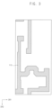
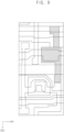
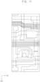
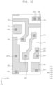
- FIGS. 3 , 4 , 5 , 6 , 7 , 8 , 9 , 10 , 11 , 12 , 13 , 14 , and 15 are layout diagrams illustrating an example of the pixel PX in FIG. 2 .
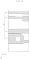
- FIG. 16 is a schematic cross-sectional view taken along a line I-I' in FIG. 13 .
- the pixel PX may include a first active layer 110, a first conductive layer 120, a second conductive layer 130, a second active layer 140, a third conductive layer 150, a fourth conductive layer 160, a fifth conductive layer 170, a first electrode 180, an emission layer 190, and a second electrode 200 which may be disposed on a substrate 100.
- the substrate 100 may be an insulating substrate including glass, quartz, plastic, or the like within the scope of the disclosure.
- the substrate 100 may include a first flexible layer, a first barrier layer disposed on the first flexible layer, a second flexible layer disposed on the first barrier layer, and a second barrier layer disposed on the second flexible layer.
- the first flexible layer and the second flexible layer may include an organic insulation material such as polyimide (PI) or the like within the scope of the disclosure.
- the first barrier layer and the second barrier layer may include an inorganic insulation material such as silicon oxide, silicon nitride, amorphous silicon, or the like within the scope of the disclosure.
- the first active layer 110 may be disposed on the substrate 100.
- the first active layer 110 may include polycrystalline silicon.
- embodiments of the disclosure are not limited thereto, and in an embodiment, the first active layer 110 may include amorphous silicon, an oxide semiconductor, or the like within the scope of the disclosure.
- a buffer layer may be disposed between the substrate 100 and the first active layer 110.
- the buffer layer may block impurities from being permeated toward above the substrate 100 through the substrate 100.
- the buffer layer may provide a planarized upper surface above the substrate 100.
- the buffer layer may include an inorganic insulation material such as silicon oxide, silicon nitride, silicon oxynitride, or the like within the scope of the disclosure.
- the buffer layer may be omitted.
- the first conductive layer 120 may be disposed on the first active layer 110.
- the first conductive layer 120 may include a conductive material such as molybdenum (Mo), copper (Cu), or the like within the scope of the disclosure.
- a first insulation layer 101 may be disposed between the first active layer 110 and the first conductive layer 120.
- the first insulation layer 101 may include an inorganic insulation material such as silicon oxide, silicon nitride, silicon oxynitride, or the like within the scope of the disclosure.
- the first conductive layer 120 may include a first gate signal line 121, an emission control signal line 122, and a conductive pattern 123.
- the first gate signal line 121 may extend in the first direction DR1.
- the emission control signal line 122 may be spaced apart from the first gate signal line 121, and may extend in the first direction DR1.
- the conductive pattern 123 may be positioned or disposed between the first gate signal line 121 and the emission control signal line 122.
- a first portion of the first gate signal line 121 overlapping the first active layer 110 may form the gate electrode of the second transistor T2, and a second portion of the first gate signal line 121 overlapping the first active layer 110 may form the gate electrode of the seventh transistor T7.
- a portion of the first active layer 110 overlapping the gate electrode of the second transistor T2 may be a channel region of the second transistor T2, and a portion of the first active layer 110 overlapping the gate electrode of the seventh transistor T7 may be a channel region of the seventh transistor T7. Accordingly, the first active layer 110 and the first portion of the first gate signal line 121 may form the second transistor T2, and the first active layer 110 and the second portion of the first gate signal line 121 may form the seventh transistor T7.
- a first portion of the emission control signal line 122 overlapping the first active layer 110 may form the gate electrode of the fifth transistor T5, and a second portion of the emission control signal line 122 overlapping the first active layer 110 may form the gate electrode of the sixth transistor T6.
- a portion of the first active layer 110 overlapping the gate electrode of the fifth transistor T5 may be a channel region of the fifth transistor T5, and a portion of the first active layer 110 overlapping the gate electrode of the sixth transistor T6 may be a channel region of the sixth transistor T6. Accordingly, the first active layer 110 and the first portion of the emission control signal line 122 may form the fifth transistor T5, and the first active layer 110 and the second portion of the emission control signal line 122 may form the sixth transistor T6.
- a portion of the conductive pattern 123 overlapping the first active layer 110 may form the gate electrode of the first transistor T1.
- a portion of the first active layer 110 overlapping the gate electrode of the first transistor T1 may be a channel region of the first transistor T1. Accordingly, the first active layer 110 and the portion of the conductive pattern 123 may form the first transistor T1.
- the second conductive layer 130 may be disposed on the first conductive layer 120.
- the second conductive layer 130 may include a conductive material such as molybdenum (Mo), copper (Cu), or the like within the scope of the disclosure.
- a second insulation layer 102 may be disposed between the first conductive layer 120 and the second conductive layer 130.
- the second insulation layer 102 may include an inorganic insulation material such as silicon oxide, silicon nitride, silicon oxynitride, or the like within the scope of the disclosure.
- the second conductive layer 130 may include a first lower gate signal line 131, a second lower gate signal line 132, the first initialization voltage line 133, and a conductive line 134.
- the first lower gate signal line 131 may extend in the first direction DR1.
- the second lower gate signal line 132 may be spaced apart from the first lower gate signal line 131, and may extend in the first direction DR1.
- the first initialization voltage line 133 may be spaced apart from the second lower gate signal line 132, and may extend in the first direction DR1.
- the conductive line 134 may be spaced apart from the first lower gate signal line 131, and may extend in the first direction DR1.
- the conductive line 134 may overlap the conductive pattern 123.
- the conductive pattern 123 and the conductive line 134 may form the capacitor CAP.
- the second active layer 140 may be disposed on the second conductive layer 130.
- the second active layer 140 may not overlap the first active layer 110.
- the second active layer 140 may include an oxide semiconductor.
- embodiments of the disclosure are not limited thereto, and in an embodiment, the second active layer 140 may include amorphous silicon, polycrystalline silicon, or the like within the scope of the disclosure.
- a third insulation layer 103 may be disposed between the second conductive layer 130 and the second active layer 140.
- the third insulation layer 103 may include an inorganic insulation material such as silicon oxide, silicon nitride, silicon oxynitride, or the like within the scope of the disclosure.
- the third conductive layer 150 may be disposed on the second active layer 140.
- the third conductive layer 150 may include a conductive material such as molybdenum (Mo), copper (Cu), or the like within the scope of the disclosure.
- a fourth insulation layer 104 may be disposed between the second active layer 140 and the third conductive layer 150.
- the fourth insulation layer 104 may include an inorganic insulation material such as silicon oxide, silicon nitride, silicon oxynitride, or the like within the scope of the disclosure.
- the third conductive layer 150 may include a first upper gate signal line 151 and a second upper gate signal line 152.
- the first upper gate signal line 151 may extend in the first direction DR1.
- the second upper gate signal line 152 may be spaced apart from the first upper gate signal line 151, and may extend in the first direction DR1.
- a portion of the first lower gate signal line 131 overlapping the second active layer 140 may form the lower gate electrode of the third transistor T3, and a portion of the first upper gate signal line 151 overlapping the second active layer 140 may form the upper gate electrode of the third transistor T3.
- a portion of the second active layer 140 overlapping the lower gate electrode and the upper gate electrode of the third transistor T3 may be a channel region of the third transistor T3. Accordingly, the portion of the first lower gate signal line 131, the second active layer 140, and the portion of the first upper gate signal line 151 may form the third transistor T3.
- the third transistor T3 may be a transistor having a double gate structure.
- a portion of the second lower gate signal line 132 overlapping the second active layer 140 may form the lower gate electrode of the fourth transistor T4, and a portion of the second upper gate signal line 152 overlapping the second active layer 140 may form the upper gate electrode of the fourth transistor T4.
- a portion of the second active layer 140 overlapping the lower gate electrode and the upper gate electrode of the fourth transistor T4 may be a channel region of the fourth transistor T4. Accordingly, the portion of the second lower gate signal line 132, the second active layer 140, and the portion of the second upper gate signal line 152 may form the fourth transistor T4.
- the fourth transistor T4 may be a transistor having a double gate structure.
- the fourth conductive layer 160 may be disposed on the third conductive layer 150.
- the fourth conductive layer 160 may include a conductive material such as aluminum (Al), titanium (Ti), copper (Cu), or the like within the scope of the disclosure.
- the fourth conductive layer 160 may have a multilayer structure including a Ti layer, an Al layer, and a Ti layer which may be stacked.
- a fifth insulation layer 105 may be disposed between the third conductive layer 150 and the fourth conductive layer 160.
- the fifth insulation layer 105 may include an inorganic insulation material such as silicon oxide, silicon nitride, silicon oxynitride, or the like and/or an organic insulation material such as polyimide (PI) or the like within the scope of the disclosure.
- the fourth conductive layer 160 may include the second initialization voltage line 161, a first connection pattern 162, a second connection pattern 163, a third connection pattern 164, a first contact pattern 165, a second contact pattern 166, and a third contact pattern 167.
- the second initialization voltage line 161 may extend in the first direction DR1.
- the second initialization voltage line 161 may be electrically connected to the first active layer 110 through a first contact hole CH1. Accordingly, the second initialization voltage line 161 may be electrically connected to the seventh transistor T7.
- the first connection pattern 162 may be spaced apart from the second initialization voltage line 161.
- the first connection pattern 162 may be electrically connected to the conductive pattern 123 through a second contact hole CH2, and may be electrically connected to the second active layer 140 through a third contact hole CH3. Accordingly, the first connection pattern 162 may electrically connect the gate electrode of the first transistor T1 and a second end portion of the third transistor T3.
- the first connection pattern 162 may electrically connect the gate electrode of the first transistor T1 and a second end portion 142 of the second active layer 140.
- the second connection pattern 163 may be spaced apart from the first connection pattern 162.
- the second connection pattern 163 may be electrically connected to the first active layer 110 through a fourth contact hole CH4, and may be electrically connected to the second active layer 140 through a fifth contact hole CH5. Accordingly, the second connection pattern 163 may electrically connect an end portion of the first transistor T1 and a first end portion of the third transistor T3.
- the second connection pattern 163 may electrically connect an end portion 111 of the first active layer 110 and a first end portion 141 of the second active layer 140.
- the third connection pattern 164 may be spaced apart from the second connection pattern 163.
- the third connection pattern 164 may be electrically connected to the first initialization voltage line 133 through a sixth contact hole CH6, and may be electrically connected to the second active layer 140 through a seventh contact hole CH7. Accordingly, the third connection pattern 164 may electrically connect the first initialization voltage line 133 and the second active layer 140.
- the first initialization voltage line 133 may be electrically connected to the fourth transistor T4 through the third connection pattern 164.
- the first contact pattern 165 may be spaced apart from the third connection pattern 164.
- the first contact pattern 165 may be electrically connected to the first active layer 110 through an eighth contact hole CH8. Accordingly, the first contact pattern 165 may be electrically connected to the second transistor T2.
- the second contact pattern 166 may be spaced apart from the first contact pattern 165.
- the second contact pattern 166 may be electrically connected to the first active layer 110 through a ninth contact hole CH9, and may be electrically connected to the conductive line 134 through a tenth contact hole CH10. Accordingly, the second contact pattern 166 may be electrically connected to the fifth transistor T5 and the capacitor CAP.
- the third contact pattern 167 may be spaced apart from the second contact pattern 166.
- the third contact pattern 167 may be electrically connected to the first active layer 110 through an eleventh contact hole CH11. Accordingly, the third contact pattern 167 may be electrically connected to the sixth transistor T6.
- the fifth conductive layer 170 may be disposed on the fourth conductive layer 160.
- the fifth conductive layer 170 may include a conductive material such as aluminum (Al), titanium (Ti), copper (Cu), or the like within the scope of the disclosure.
- the fifth conductive layer 170 may have a multilayer structure including a Ti layer, an Al layer, and a Ti layer which may be stacked.
- a sixth insulation layer 106 may be disposed between the fourth conductive layer 160 and the fifth conductive layer 170.
- the sixth insulation layer 106 may include an inorganic insulation material such as silicon oxide, silicon nitride, silicon oxynitride, or the like and/or an organic insulation material such as polyimide (PI) or the like within the scope of the disclosure.
- the fifth conductive layer 170 may include the data line 171, the power voltage line 172, and a fourth contact pattern 173.
- the data line 171 may extend in the second direction DR2.
- the date line 171 may be electrically connected to the first contact pattern 165 through a twelfth contact hole CH12. Accordingly, the date line 171 may be electrically connected to the second transistor T2 through the first contact pattern 165.
- the power voltage line 172 may be spaced apart from the date line 171, and may extend in the second direction DR2.
- the power voltage line 172 may be electrically connected to the second contact pattern 162 through a thirteenth contact hole CH13. Accordingly, the power voltage line 172 may be electrically connected to the fifth transistor T5 and the capacitor CAP through the second contact pattern 166.
- the fourth contact pattern 173 may be spaced apart from the power voltage line 172.
- the fourth contact pattern 173 may be electrically connected to the third contact pattern 167 through a fourteenth contact hole CH14.
- the first electrode 180 may be disposed on the fifth conductive layer 170.
- the first electrode 180 may include a conductive material such as a metal, an alloy, a transparent conductive oxide, or the like within the scope of the disclosure.
- the first electrode 180 may include silver (Ag), indium tin oxide (ITO), or the like within the scope of the disclosure.
- the first electrode 180 may have a multilayer structure including an ITO layer, an Ag layer, and an ITO layer which may be stacked.
- a seventh insulation layer 107 may be disposed between the fifth conductive layer 170 and the first electrode 180.
- the seventh insulation layer 107 may include an inorganic insulation material such as silicon oxide, silicon nitride, silicon oxynitride, or the like and/or an organic insulation material such as polyimide (PI) or the like within the of the disclosure.
- the first electrode 180 may be electrically connected to the fourth contact pattern 173 through a contact hole. Accordingly, the first electrode 180 may be electrically connected to the sixth transistor T6 through the third contact pattern 167 and the fourth contact pattern 173.
- An eighth insulation layer 108 may be disposed on the first electrode 180.
- the eighth insulation layer 108 may cover or overlap the first electrode 180, and may be disposed on the seventh insulation layer 107.
- the eighth insulation layer 108 may have a pixel opening exposing at least a portion of the first electrode 180. In an embodiment, the pixel opening may expose a central portion of the first electrode 180, and the eighth insulation layer 108 may cover or overlap a peripheral portion of the first electrode 180.
- the eighth insulation layer 108 may include an organic insulation material such as polyimide (PI) or the like within the scope of the disclosure.
- the emission layer 190 may be disposed on the first electrode 180.
- the emission layer 190 may be disposed on the first electrode 180 exposed by the pixel opening.
- the emission layer 190 may include at least one of an organic light emitting material and a quantum dot.
- the organic light emitting material may include a low molecular organic compound or a high molecular organic compound.
- the low molecular organic compound may include copper phthalocyanine, diphenylbenzidine (N, N'-diphenylbenzidine), trihydroxyquinoline aluminum (tris-(8-hydroxyquinoline)aluminum), and the like within the scope of the disclosure.
- the high molecular organic compound may include poly ethylenedioxythiophene (poly(3,4-ethylenedioxythiophene), polyaniline, polyphenylenevinylene, polyfluorene, and the like within the scope of the disclosure.
- the quantum dot may include a core including a group II-VI compound, a group III-V compound, a group IV-VI compound, a group IV element, a group IV compound, and a combination thereof.
- the quantum dot may have a core-shell structure including a core and a shell surrounding the core. The shell may prevent chemical denaturation of the core, thereby serving as a protective layer for maintaining semiconductor characteristics and a charging layer for imparting electrophoretic characteristics to the quantum dot.
- the second electrode 200 may be disposed on the emission layer 190. In an embodiment, the second electrode 200 may also be disposed on the eighth insulation layer 108.
- the second electrode 200 may include a conductive material such as a metal, an alloy, a transparent conductive oxide, or the like within the scope of the disclosure.
- the second electrode 200 may include aluminum (Al), platinum (Pt), silver (Ag), magnesium (Mg), gold (Au), chromium (Cr), tungsten (W), titanium (Ti), or the like within the scope of the disclosure.
- the first electrode 180, the emission layer 190, and the second electrode 200 may form the light emitting element EL.
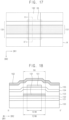
- FIG. 17 is a layout diagram illustrating an example of an area A in FIG. 13 .
- FIG. 18 is a schematic cross-sectional view taken along a line II-II' in FIG. 17 .
- the first upper gate signal line 151 may be disposed on the first lower gate signal line 131, and the first connection pattern 162 may be disposed on the first upper gate signal line 151.
- the first connection pattern 162 may cross or intersect the first lower gate signal line 131 and the first upper gate signal line 151 which may extend in the first direction DR1.
- An area in which the first lower gate signal line 131 or the first upper gate signal line 151 may overlap the first connection pattern 162 may be defined as an overlapping area OA.
- the first connection pattern 162 may extend in the second direction DR2 in the overlapping area OA.
- a width 151W of the first upper gate signal line 151 in the second direction DR2 may be less than a width 131W of the first lower gate signal line 131 in the second direction DR2 in the overlapping area OA.
- An entirety of the first upper gate signal line 151 may overlap a part of the first lower gate signal line 131 in the overlapping area OA.
- a portion of the first lower gate signal line 131 may overlap the first upper gate signal line 151 in the overlapping area OA, and another portion of the first lower gate signal line 131 may not overlap the first upper gate signal line 151 in the overlapping area OA.
- a central portion of the first lower gate signal line 131 in the second direction DR2 may overlap the first upper gate signal line 151 in the overlapping area OA, and side portions of the first lower gate signal line 131 in the second direction DR2 may not overlap the first upper gate signal line 151 in the overlapping area OA.
- the width 151W of the first upper gate signal line 151 in the second direction DR2 may be less than the width 131W of the first lower gate signal line 131 in the second direction DR2 in the overlapping area OA, and an entirety of the first upper gate signal line 151 may overlap a part of the first lower gate signal line 131 in the overlapping area OA.
- a capacitance between the first lower gate signal line 131 and the first connection pattern 162 and a capacitance between the first upper gate signal line 151 and the first connection pattern 162 may be constantly maintained.
- a value subtracting the width 151W of the first upper gate signal line 151 in the second direction DR2 from the width 131W of the first lower gate signal line 131 in the second direction DR2 in the overlapping area OA may be greater than about 1 ⁇ m.
- the difference between the width 131W of the first lower gate signal line 131 in the second direction DR2 in the overlapping area OA and the width 151W of the first upper gate signal line 151 in the second direction DR2 may be greater than about 1 ⁇ m.
- a tolerance less than about 0.5 ⁇ m in the second direction DR2 may occur in the process of forming the first upper gate signal line 151 on the first lower gate signal line 131.
- the value subtracting the width 151W of the first upper gate signal line 151 in the second direction DR2 from the width 131W of the first lower gate signal line 131 in the second direction DR2 may be greater than about 1 ⁇ m in the overlapping area OA, although the tolerance less than about 0.5 ⁇ m in the second direction DR2 may occur in the process of forming the first upper gate signal line 151 on the first lower gate signal line 131, an entirety of the first upper gate signal line 151 may overlap a part of the first lower gate signal line 131 in the overlapping area OA.
- each of a width of the first lower gate signal line 131 in the second direction DR2 and a width of the first upper gate signal line 151 in the second direction DR2 may be constant.
- a width of the first lower gate signal line 131 in the second direction DR2 outside the overlapping area OA may be substantially equal to the width 131W of the first lower gate signal line 131 in the second direction DR2 inside the overlapping area OA
- a width of the first upper gate signal line 151 in the second direction DR2 outside the overlapping area OA may be substantially equal to the width 151W of the first upper gate signal line 151 in the second direction DR2 inside the overlapping area OA.
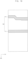
- FIG. 19 is a layout diagram illustrating an example of the area A in FIG. 13 .
- FIG. 20 is a layout diagram illustrating an example of the area A in FIG. 13 .
- the first lower gate signal line 131 may protrude in the second direction DR2 in a plan view in the overlapping area OA.
- a portion of the first upper gate signal line 151 outside the overlapping area OA may not overlap the first lower gate signal line 131, and the first lower gate signal line 131 may have a protruding portion 131P protruding in the second direction DR2 in the overlapping area OA.
- a width of the first lower gate signal line 131 in the second direction DR2 outside the overlapping area OA may be less than a width 131W of the first lower gate signal line 131 in the second direction DR2 inside the overlapping area OA, and a width of the first upper gate signal line 151 in the second direction DR2 outside the overlapping area OA may be substantially equal to a width 151W of the first upper gate signal line 151 in the second direction DR2 inside the overlapping area OA.
- the first upper gate signal line 151 may be recessed in the second direction DR2 in a plan view in the overlapping area OA.
- a portion of the first upper gate signal line 151 outside the overlapping area OA may not overlap the first lower gate signal line 131, and the first upper gate signal line 151 may have a recessed portion 151R recessed in the second direction DR2 in the overlapping area OA.
- a width of the first lower gate signal line 131 in the second direction DR2 outside the overlapping area OA may be substantially equal to a width 131W of the first lower gate signal line 131 in the second direction DR2 inside the overlapping area OA, and a width of the first upper gate signal line 151 in the second direction DR2 outside the overlapping area OA may be greater than a width 151W of the first upper gate signal line 151 in the second direction DR2 inside the overlapping area OA.
- FIG. 21 is a diagram illustrating a kickback voltage of the third node N3 based on the second gate signal GS2.
- the second node N2 and the third node N3 may be electrically connected to each other such that the first transistor T1 may be diode-connected. Then, in a case that the second transistor T2 is turned-on based on the first gate signal GS1, the data voltage DV may be applied to the first node N1, therefore, a voltage V_N3 in which a threshold voltage of the first transistor T1 may be compensated from the data voltage DV may be applied to the third node N3. Then, in a case that the second gate signal GS2 is changed from the high level to the low level, the voltage V_N3 of the third node N3 may be increase or decrease as much as a kickback voltage V_KB.
- the first lower gate signal line 131 and the first connection pattern 162 may electrically affect the first connection pattern 162.
- the voltage V_N3 of the first connection pattern 162 that may be the third node N3 may increase or decrease as much as the kickback voltage V_KB.
- kickback voltages V_KB occurred in pixel rows may be different from each other, stains may occur in the display device.
- kickback voltages V_KB may be constantly maintained, because the capacitance between the first lower gate signal line 131 and the first connection pattern 162 and the capacitance between the first upper gate signal line 151 and the first connection pattern 162 may be constantly maintained, kickback voltages V_KB that occurred in pixel rows may be substantially equal to each other, therefore, stains may not occur in the display device, and display quality of the display device may be improved.
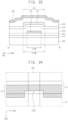
- FIG. 22 is a layout diagram illustrating an example of the area A in FIG. 13 .
- FIG. 23 is a schematic cross-sectional view taken along a line III-III' in FIG. 22 .
- a width 151W of the first upper gate signal line 151 in the second direction DR2 may be greater than a width 131W of the first lower gate signal line 131 in the second direction DR2 in the overlapping area OA.
- An entirety of the first lower gate signal line 131 may overlap a part of the first upper gate signal line 151 in the overlapping area OA.
- a portion of the first upper gate signal line 151 may overlap the first lower gate signal line 131 in the overlapping area OA, and another portion of the first upper gate signal line 151 may not overlap the first lower gate signal line 131 in the overlapping area OA.
- a central portion of the first upper gate signal line 151 in the second direction DR2 may overlap the first lower gate signal line 131 in the overlapping area OA, and side portions of the first upper gate signal line 151 in the second direction DR2 may not overlap the first lower gate signal line 131 in the overlapping area OA.
- the width 151W of the first upper gate signal line 151 in the second direction DR2 may be greater than the width 131W of the first lower gate signal line 131 in the second direction DR2 in the overlapping area OA, and an entirety of the first lower gate signal line 131 may overlap a part of the first upper gate signal line 151 in the overlapping area OA. Therefore, although tolerance in the process of forming the first upper gate signal line 151 on the first lower gate signal line 131 is considered, the first upper gate signal line 151 may shield the first lower gate signal line 131 from the first connection pattern 162. Accordingly, a capacitance between the first lower gate signal line 131 and the first connection pattern 162 and a capacitance between the first upper gate signal line 151 and the first connection pattern 162 may be constantly maintained.
- a value subtracting the width 131W of the first lower gate signal line 131 in the second direction DR2 from the width 151W of the first upper gate signal line 151 in the second direction DR2 in the overlapping area OA may be greater than about 1 ⁇ m.
- the difference between the width 151W of the first upper gate signal line 151 in the second direction DR2 in the overlapping area OA and the width 131W of the first lower gate signal line 131 in the second direction DR2 may be greater than about 1 ⁇ m.
- a tolerance less than about 0.5 ⁇ m in the second direction DR2 may occur in the process of forming the first upper gate signal line 151 on the first lower gate signal line 131.
- the value subtracting the width 131W of the first lower gate signal line 131 in the second direction DR2 from the width 151W of the first upper gate signal line 151 in the second direction DR2 is greater than about 1 ⁇ m in the overlapping area OA, although the tolerance less than about 0.5 ⁇ m in the second direction DR2 may occur in the process of forming the first upper gate signal line 151 on the first lower gate signal line 131, an entirety of the first lower gate signal line 131 may overlap a part of the first upper gate signal line 151 in the overlapping area OA.
- each of a width of the first lower gate signal line 131 in the second direction DR2 and a width of the first upper gate signal line 151 in the second direction DR2 may be constant.
- a width of the first lower gate signal line 131 in the second direction DR2 outside the overlapping area OA may be substantially equal to the width 131W of the first lower gate signal line 131 in the second direction DR2 inside the overlapping area OA
- a width of the first upper gate signal line 151 in the second direction DR2 outside the overlapping area OA may be substantially equal to the width 151W of the first upper gate signal line 151 in the second direction DR2 inside the overlapping area OA.
- the widths of the first lower gate signal line 131 both inside and outside of the overlapping area OA in the second direction DR2 may be substantially equal.
- the widths of the first upper gate signal line 151 both inside and outside of the overlapping area OA in the second direction DR2 may be substantially equal.
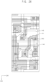
- FIG. 24 is a layout diagram illustrating an example of the area A in FIG. 13 .
- FIG. 25 is a layout diagram illustrating an example of the area A in FIG. 13 .
- the first lower gate signal line 131 may be recessed in the second direction DR2 in a plan view in the overlapping area OA.
- a portion of the first lower gate signal line 131 outside the overlapping area OA may not overlap the first upper gate signal line 151, and the first lower gate signal line 131 may have a recessed portion 131R recessed in the second direction DR2 in the overlapping area OA.
- a width of the first lower gate signal line 131 in the second direction DR2 outside the overlapping area OA may be greater than a width 131W of the first lower gate signal line 131 in the second direction DR2 inside the overlapping area OA, and a width of the first upper gate signal line 151 in the second direction DR2 outside the overlapping area OA may be substantially equal to a width 151W of the first upper gate signal line 151 in the second direction DR2 inside the overlapping area OA.
- the first upper gate signal line 151 may protrude in the second direction DR2 in a plan view in the overlapping area OA.
- a portion of the first lower gate signal line 131 outside the overlapping area OA may not overlap the first upper gate signal line 151, and the first upper gate signal line 151 may have a protruding portion 151P protruding in the second direction DR2 in the overlapping area OA.
- a width of the first lower gate signal line 131 in the second direction DR2 outside the overlapping area OA may be substantially equal to a width 131W of the first lower gate signal line 131 in the second direction DR2 inside the overlapping area OA, and a width of the first upper gate signal line 151 in the second direction DR2 outside the overlapping area OA may be less than a width 151W of the first upper gate signal line 151 in the second direction DR2 inside the overlapping area OA.
- the third contact hole CH3 electrically connecting the second active layer 140 and the first connection pattern 1162 may not overlap the first gate signal line 121.
- the third contact hole CH3 and the first gate signal line 121 may be spaced apart from each other in a plan view. Accordingly, a path for compensating the threshold voltage of the first transistor T1 through the second active layer 140, the third contact hole CH3, and the first connection pattern 1162 may not overlap the first gate signal line 121 transmitting the first gate signal.
- embodiments can provide a display device, comprising: a first transistor including a gate electrode disposed over a substrate; a second transistor including: a lower gate electrode disposed over the substrate; an upper gate electrode disposed over the lower gate electrode; and a first end portion electrically connected to an end portion of the first transistor; a lower gate signal line extending in a first direction, a portion of the lower gate signal line forming the lower gate electrode; an upper gate signal line disposed over the lower gate signal line and extending in the first direction, a portion of the upper gate signal line forming the upper gate electrode; and a first connection pattern disposed over the upper gate signal line, electrically connecting the gate electrode and a second end portion of the second transistor, and intersecting the lower gate signal line and the upper gate signal line, wherein an entirety of the upper gate signal line overlaps a part of the lower gate signal line in an overlapping area in which the lower gate signal line or the upper gate signal line overlaps the first connection pattern.
- the first transistor may comprise a first active layer disposed over the substrate.
- a first conductive layer may be disposed over the first active layer.
- the first conductive layer may include a conductive pattern.
- the first conductive layer may include a first gate signal line, an emission control signal line, and the conductive pattern.
- a portion of the conductive pattern overlapping the first active layer may form the gate electrode of the first transistor.
- a portion of the first active layer overlapping the gate electrode of the first transistor may be a channel region of the first transistor. Accordingly, the first active layer and the portion of the conductive pattern may form the first transistor.
- the first connection pattern may be part of a conductive layer.
- a conductive layer may include the first connection pattern and a second connection pattern.
- the second transistor may include a second active layer.
- the second active layer does not overlap the first active layer.
- a portion of the lower gate signal line overlapping the second active layer may form the lower gate electrode of the second transistor, and a portion of the upper gate signal line overlapping the second active layer may form the upper gate electrode of the second transistor.
- a portion of the second active layer overlapping the lower gate electrode and the upper gate electrode of the second transistor may be a channel region of the second transistor. Accordingly, the portion of the first lower gate signal line, the second active layer, and the portion of the first upper gate signal line may form the second transistor.
- the second transistor may be a transistor having a double gate structure.
- the first connection pattern may be electrically connected to the conductive pattern that forms the gate of the first transistor through a contact hole, and may be electrically connected to the second active layer through a contact hole. Accordingly, the first connection pattern may electrically connect the gate electrode of the first transistor and a second end portion of the second transistor. For example, the first connection pattern may electrically connect the gate electrode of the first transistor and a second end portion of the second active layer.
- the second connection pattern may be spaced apart from the first connection pattern.
- the second connection pattern may be electrically connected to the first active layer through a contact hole, and may be electrically connected to the second active layer through a contact hole. Accordingly, the second connection pattern may electrically connect an end portion of the first transistor and a first end portion of the second transistor. As an example, the second connection pattern may electrically connect an end portion of the first active layer and a first end portion of the second active layer.
- embodiments can provide a display device, comprising: a first transistor including a gate electrode disposed over a substrate; a second transistor including: a lower gate electrode disposed over the substrate; an upper gate electrode disposed over the lower gate electrode; and a first end portion electrically connected to an end portion of the first transistor; a lower gate signal line extending in a first direction, a portion of the lower gate signal line forming the lower gate electrode; an upper gate signal line disposed over the lower gate signal line and extending in the first direction, a portion of the upper gate signal line forming the upper gate electrode; and a first connection pattern disposed over the upper gate signal line, electrically connecting the gate electrode and a second end portion of the second transistor, and intersecting the lower gate signal line and the upper gate signal line, wherein an entirety of the lower gate signal line overlaps a part of the upper gate signal line in an overlapping area in which the lower gate signal line or the upper gate signal line overlaps the first connection pattern.
- the display device may be applied to a display device included in a computer, a notebook, a mobile phone, a smartphone, a smart pad, a PMP, a PDA, an MP3 player, or the like within the scope of the disclosure.
Landscapes
- Engineering & Computer Science (AREA)
- Physics & Mathematics (AREA)
- Microelectronics & Electronic Packaging (AREA)
- General Physics & Mathematics (AREA)
- Theoretical Computer Science (AREA)
- Computer Hardware Design (AREA)
- Nonlinear Science (AREA)
- Geometry (AREA)
- Chemical & Material Sciences (AREA)
- Crystallography & Structural Chemistry (AREA)
- Mathematical Physics (AREA)
- Optics & Photonics (AREA)
- Devices For Indicating Variable Information By Combining Individual Elements (AREA)
- Thin Film Transistor (AREA)
- Electroluminescent Light Sources (AREA)
Applications Claiming Priority (2)
| Application Number | Priority Date | Filing Date | Title |
|---|---|---|---|
| KR1020200034543A KR102774516B1 (ko) | 2020-03-20 | 2020-03-20 | 표시 장치 |
| EP21153087.8A EP3882970B1 (de) | 2020-03-20 | 2021-01-22 | Anzeigevorrichtung |
Related Parent Applications (2)
| Application Number | Title | Priority Date | Filing Date |
|---|---|---|---|
| EP21153087.8A Division EP3882970B1 (de) | 2020-03-20 | 2021-01-22 | Anzeigevorrichtung |
| EP21153087.8A Division-Into EP3882970B1 (de) | 2020-03-20 | 2021-01-22 | Anzeigevorrichtung |
Publications (2)
| Publication Number | Publication Date |
|---|---|
| EP4465796A2 true EP4465796A2 (de) | 2024-11-20 |
| EP4465796A3 EP4465796A3 (de) | 2025-02-19 |
Family
ID=74215764
Family Applications (2)
| Application Number | Title | Priority Date | Filing Date |
|---|---|---|---|
| EP21153087.8A Active EP3882970B1 (de) | 2020-03-20 | 2021-01-22 | Anzeigevorrichtung |
| EP24204384.2A Pending EP4465796A3 (de) | 2020-03-20 | 2021-01-22 | Anzeigevorrichtung |
Family Applications Before (1)
| Application Number | Title | Priority Date | Filing Date |
|---|---|---|---|
| EP21153087.8A Active EP3882970B1 (de) | 2020-03-20 | 2021-01-22 | Anzeigevorrichtung |
Country Status (4)
| Country | Link |
|---|---|
| US (4) | US11296234B2 (de) |
| EP (2) | EP3882970B1 (de) |
| KR (3) | KR102774516B1 (de) |
| CN (2) | CN118398629A (de) |
Families Citing this family (2)
| Publication number | Priority date | Publication date | Assignee | Title |
|---|---|---|---|---|
| KR20220149879A (ko) | 2021-04-30 | 2022-11-09 | 삼성디스플레이 주식회사 | 표시 장치 |
| WO2023230870A1 (zh) * | 2022-05-31 | 2023-12-07 | 京东方科技集团股份有限公司 | 显示基板及显示装置 |
Family Cites Families (14)
| Publication number | Priority date | Publication date | Assignee | Title |
|---|---|---|---|---|
| TWI545380B (zh) * | 2006-05-16 | 2016-08-11 | 半導體能源研究所股份有限公司 | 液晶顯示裝置和半導體裝置 |
| JP4315172B2 (ja) | 2006-07-12 | 2009-08-19 | セイコーエプソン株式会社 | 電気光学装置用基板の製造方法 |
| US8629842B2 (en) | 2008-07-11 | 2014-01-14 | Samsung Display Co., Ltd. | Organic light emitting display device |
| US8300163B2 (en) * | 2008-08-28 | 2012-10-30 | Sharp Kabushiki Kaisha | Display panel, display device, and television receiver |
| JP5442234B2 (ja) | 2008-10-24 | 2014-03-12 | 株式会社半導体エネルギー研究所 | 半導体装置及び表示装置 |
| KR102258374B1 (ko) * | 2013-10-18 | 2021-06-01 | 삼성디스플레이 주식회사 | 박막 트랜지스터, 이를 포함하는 표시 패널 및 이의 제조 방법 |
| KR102241704B1 (ko) * | 2014-08-07 | 2021-04-20 | 삼성디스플레이 주식회사 | 화소 회로 및 이를 포함하는 유기 발광 표시 장치 |
| KR102483953B1 (ko) * | 2015-10-16 | 2023-01-03 | 삼성디스플레이 주식회사 | 박막트랜지스터 기판 및 이를 구비한 유기 발광 표시 장치 |
| KR102730433B1 (ko) | 2016-09-02 | 2024-11-14 | 삼성디스플레이 주식회사 | 유기 발광 표시 장치 |
| US10916617B2 (en) | 2018-05-04 | 2021-02-09 | Samsung Display Co., Ltd. | Display device |
| KR102670595B1 (ko) * | 2018-06-19 | 2024-06-03 | 삼성디스플레이 주식회사 | 표시장치 |
| KR102711314B1 (ko) | 2018-06-28 | 2024-09-27 | 삼성디스플레이 주식회사 | 유기 발광 표시 장치 |
| KR20200016425A (ko) * | 2018-08-06 | 2020-02-17 | 삼성디스플레이 주식회사 | 유기발광 표시 장치 |
| JP7284613B2 (ja) * | 2019-03-29 | 2023-05-31 | シャープ株式会社 | アクティブマトリクス基板およびその製造方法 |
-
2020
- 2020-03-20 KR KR1020200034543A patent/KR102774516B1/ko active Active
- 2020-10-14 US US17/070,503 patent/US11296234B2/en active Active
-
2021
- 2021-01-05 CN CN202410617225.5A patent/CN118398629A/zh active Pending
- 2021-01-05 CN CN202110007113.4A patent/CN113497098B/zh active Active
- 2021-01-22 EP EP21153087.8A patent/EP3882970B1/de active Active
- 2021-01-22 EP EP24204384.2A patent/EP4465796A3/de active Pending
-
2022
- 2022-03-03 US US17/685,733 patent/US11769835B2/en active Active
-
2023
- 2023-08-08 US US18/366,896 patent/US12199185B2/en active Active
-
2025
- 2025-01-03 US US19/009,354 patent/US20250142889A1/en active Pending
- 2025-02-21 KR KR1020250022650A patent/KR102907149B1/ko active Active
- 2025-12-29 KR KR1020250212281A patent/KR20260005860A/ko active Pending
Also Published As
| Publication number | Publication date |
|---|---|
| US11769835B2 (en) | 2023-09-26 |
| KR20210118330A (ko) | 2021-09-30 |
| CN113497098B (zh) | 2026-03-27 |
| US20250142889A1 (en) | 2025-05-01 |
| CN113497098A (zh) | 2021-10-12 |
| KR102774516B1 (ko) | 2025-03-05 |
| US12199185B2 (en) | 2025-01-14 |
| US20240021731A1 (en) | 2024-01-18 |
| CN118398629A (zh) | 2024-07-26 |
| EP3882970A1 (de) | 2021-09-22 |
| EP4465796A3 (de) | 2025-02-19 |
| US11296234B2 (en) | 2022-04-05 |
| US20220190165A1 (en) | 2022-06-16 |
| KR102907149B1 (ko) | 2026-01-05 |
| US20210296502A1 (en) | 2021-09-23 |
| EP3882970B1 (de) | 2024-11-13 |
| KR20260005860A (ko) | 2026-01-12 |
| KR20250029099A (ko) | 2025-03-04 |
Similar Documents
| Publication | Publication Date | Title |
|---|---|---|
| US20250142889A1 (en) | Display device | |
| US20250166569A1 (en) | Pixel circuit and display device including the same | |
| US11404519B2 (en) | Organic light emitting display device | |
| US20210320165A1 (en) | Display device | |
| US11856826B2 (en) | Display device | |
| US12414440B2 (en) | Display device | |
| US12029080B2 (en) | Display device | |
| US12057059B2 (en) | Display substrate and mother substrate for display substrate | |
| US12150347B2 (en) | Display device having an opening in an insulating layer exposing an conductive layer and method of manufacturing the same | |
| KR20230135730A (ko) | 디스플레이 장치 | |
| KR20230007578A (ko) | 표시 장치 및 표시 장치의 제조 방법 | |
| US12396337B2 (en) | Display device | |
| US20240113136A1 (en) | Display device | |
| US12178081B2 (en) | Display device | |
| US20240179979A1 (en) | Display apparatus |
Legal Events
| Date | Code | Title | Description |
|---|---|---|---|
| PUAI | Public reference made under article 153(3) epc to a published international application that has entered the european phase |
Free format text: ORIGINAL CODE: 0009012 |
|
| STAA | Information on the status of an ep patent application or granted ep patent |
Free format text: STATUS: THE APPLICATION HAS BEEN PUBLISHED |
|
| AC | Divisional application: reference to earlier application |
Ref document number: 3882970 Country of ref document: EP Kind code of ref document: P |
|
| AK | Designated contracting states |
Kind code of ref document: A2 Designated state(s): AL AT BE BG CH CY CZ DE DK EE ES FI FR GB GR HR HU IE IS IT LI LT LU LV MC MK MT NL NO PL PT RO RS SE SI SK SM TR |
|
| REG | Reference to a national code |
Ref country code: DE Ref legal event code: R079 Free format text: PREVIOUS MAIN CLASS: H10K0059131000 Ipc: H10D0086400000 |
|
| PUAL | Search report despatched |
Free format text: ORIGINAL CODE: 0009013 |
|
| AK | Designated contracting states |
Kind code of ref document: A3 Designated state(s): AL AT BE BG CH CY CZ DE DK EE ES FI FR GB GR HR HU IE IS IT LI LT LU LV MC MK MT NL NO PL PT RO RS SE SI SK SM TR |
|
| RIC1 | Information provided on ipc code assigned before grant |
Ipc: H10K 59/131 20230101ALI20250110BHEP Ipc: H10D 86/60 20250101ALI20250110BHEP Ipc: H10D 86/40 20250101AFI20250110BHEP |
|
| STAA | Information on the status of an ep patent application or granted ep patent |
Free format text: STATUS: REQUEST FOR EXAMINATION WAS MADE |
|
| 17P | Request for examination filed |
Effective date: 20250718 |
|
| P01 | Opt-out of the competence of the unified patent court (upc) registered |
Free format text: CASE NUMBER: UPC_APP_0007503_4465796/2026 Effective date: 20260226 |