EP4465290A2 - Treiber und anzeigevorrichtung - Google Patents
Treiber und anzeigevorrichtung Download PDFInfo
- Publication number
- EP4465290A2 EP4465290A2 EP24161087.2A EP24161087A EP4465290A2 EP 4465290 A2 EP4465290 A2 EP 4465290A2 EP 24161087 A EP24161087 A EP 24161087A EP 4465290 A2 EP4465290 A2 EP 4465290A2
- Authority
- EP
- European Patent Office
- Prior art keywords
- node
- oxide
- voltage
- driver
- type metal
- Prior art date
- Legal status (The legal status is an assumption and is not a legal conclusion. Google has not performed a legal analysis and makes no representation as to the accuracy of the status listed.)
- Pending
Links
Images











Classifications
-
- G—PHYSICS
- G09—EDUCATION; CRYPTOGRAPHY; DISPLAY; ADVERTISING; SEALS
- G09G—ARRANGEMENTS OR CIRCUITS FOR CONTROL OF INDICATING DEVICES USING STATIC MEANS TO PRESENT VARIABLE INFORMATION
- G09G3/00—Control arrangements or circuits, of interest only in connection with visual indicators other than cathode-ray tubes
- G09G3/20—Control arrangements or circuits, of interest only in connection with visual indicators other than cathode-ray tubes for presentation of an assembly of a number of characters, e.g. a page, by composing the assembly by combination of individual elements arranged in a matrix no fixed position being assigned to or needed to be assigned to the individual characters or partial characters
- G09G3/22—Control arrangements or circuits, of interest only in connection with visual indicators other than cathode-ray tubes for presentation of an assembly of a number of characters, e.g. a page, by composing the assembly by combination of individual elements arranged in a matrix no fixed position being assigned to or needed to be assigned to the individual characters or partial characters using controlled light sources
- G09G3/30—Control arrangements or circuits, of interest only in connection with visual indicators other than cathode-ray tubes for presentation of an assembly of a number of characters, e.g. a page, by composing the assembly by combination of individual elements arranged in a matrix no fixed position being assigned to or needed to be assigned to the individual characters or partial characters using controlled light sources using electroluminescent panels
- G09G3/32—Control arrangements or circuits, of interest only in connection with visual indicators other than cathode-ray tubes for presentation of an assembly of a number of characters, e.g. a page, by composing the assembly by combination of individual elements arranged in a matrix no fixed position being assigned to or needed to be assigned to the individual characters or partial characters using controlled light sources using electroluminescent panels semiconductive, e.g. using light-emitting diodes [LED]
-
- G—PHYSICS
- G09—EDUCATION; CRYPTOGRAPHY; DISPLAY; ADVERTISING; SEALS
- G09G—ARRANGEMENTS OR CIRCUITS FOR CONTROL OF INDICATING DEVICES USING STATIC MEANS TO PRESENT VARIABLE INFORMATION
- G09G3/00—Control arrangements or circuits, of interest only in connection with visual indicators other than cathode-ray tubes
- G09G3/20—Control arrangements or circuits, of interest only in connection with visual indicators other than cathode-ray tubes for presentation of an assembly of a number of characters, e.g. a page, by composing the assembly by combination of individual elements arranged in a matrix no fixed position being assigned to or needed to be assigned to the individual characters or partial characters
- G09G3/22—Control arrangements or circuits, of interest only in connection with visual indicators other than cathode-ray tubes for presentation of an assembly of a number of characters, e.g. a page, by composing the assembly by combination of individual elements arranged in a matrix no fixed position being assigned to or needed to be assigned to the individual characters or partial characters using controlled light sources
- G09G3/30—Control arrangements or circuits, of interest only in connection with visual indicators other than cathode-ray tubes for presentation of an assembly of a number of characters, e.g. a page, by composing the assembly by combination of individual elements arranged in a matrix no fixed position being assigned to or needed to be assigned to the individual characters or partial characters using controlled light sources using electroluminescent panels
- G09G3/32—Control arrangements or circuits, of interest only in connection with visual indicators other than cathode-ray tubes for presentation of an assembly of a number of characters, e.g. a page, by composing the assembly by combination of individual elements arranged in a matrix no fixed position being assigned to or needed to be assigned to the individual characters or partial characters using controlled light sources using electroluminescent panels semiconductive, e.g. using light-emitting diodes [LED]
- G09G3/3208—Control arrangements or circuits, of interest only in connection with visual indicators other than cathode-ray tubes for presentation of an assembly of a number of characters, e.g. a page, by composing the assembly by combination of individual elements arranged in a matrix no fixed position being assigned to or needed to be assigned to the individual characters or partial characters using controlled light sources using electroluminescent panels semiconductive, e.g. using light-emitting diodes [LED] organic, e.g. using organic light-emitting diodes [OLED]
- G09G3/3266—Details of drivers for scan electrodes
-
- G—PHYSICS
- G09—EDUCATION; CRYPTOGRAPHY; DISPLAY; ADVERTISING; SEALS
- G09G—ARRANGEMENTS OR CIRCUITS FOR CONTROL OF INDICATING DEVICES USING STATIC MEANS TO PRESENT VARIABLE INFORMATION
- G09G3/00—Control arrangements or circuits, of interest only in connection with visual indicators other than cathode-ray tubes
- G09G3/20—Control arrangements or circuits, of interest only in connection with visual indicators other than cathode-ray tubes for presentation of an assembly of a number of characters, e.g. a page, by composing the assembly by combination of individual elements arranged in a matrix no fixed position being assigned to or needed to be assigned to the individual characters or partial characters
- G09G3/2092—Details of a display terminals using a flat panel, the details relating to the control arrangement of the display terminal and to the interfaces thereto
- G09G3/2096—Details of the interface to the display terminal specific for a flat panel
-
- G—PHYSICS
- G09—EDUCATION; CRYPTOGRAPHY; DISPLAY; ADVERTISING; SEALS
- G09G—ARRANGEMENTS OR CIRCUITS FOR CONTROL OF INDICATING DEVICES USING STATIC MEANS TO PRESENT VARIABLE INFORMATION
- G09G3/00—Control arrangements or circuits, of interest only in connection with visual indicators other than cathode-ray tubes
- G09G3/20—Control arrangements or circuits, of interest only in connection with visual indicators other than cathode-ray tubes for presentation of an assembly of a number of characters, e.g. a page, by composing the assembly by combination of individual elements arranged in a matrix no fixed position being assigned to or needed to be assigned to the individual characters or partial characters
- G09G3/22—Control arrangements or circuits, of interest only in connection with visual indicators other than cathode-ray tubes for presentation of an assembly of a number of characters, e.g. a page, by composing the assembly by combination of individual elements arranged in a matrix no fixed position being assigned to or needed to be assigned to the individual characters or partial characters using controlled light sources
- G09G3/30—Control arrangements or circuits, of interest only in connection with visual indicators other than cathode-ray tubes for presentation of an assembly of a number of characters, e.g. a page, by composing the assembly by combination of individual elements arranged in a matrix no fixed position being assigned to or needed to be assigned to the individual characters or partial characters using controlled light sources using electroluminescent panels
- G09G3/32—Control arrangements or circuits, of interest only in connection with visual indicators other than cathode-ray tubes for presentation of an assembly of a number of characters, e.g. a page, by composing the assembly by combination of individual elements arranged in a matrix no fixed position being assigned to or needed to be assigned to the individual characters or partial characters using controlled light sources using electroluminescent panels semiconductive, e.g. using light-emitting diodes [LED]
- G09G3/3208—Control arrangements or circuits, of interest only in connection with visual indicators other than cathode-ray tubes for presentation of an assembly of a number of characters, e.g. a page, by composing the assembly by combination of individual elements arranged in a matrix no fixed position being assigned to or needed to be assigned to the individual characters or partial characters using controlled light sources using electroluminescent panels semiconductive, e.g. using light-emitting diodes [LED] organic, e.g. using organic light-emitting diodes [OLED]
-
- G—PHYSICS
- G09—EDUCATION; CRYPTOGRAPHY; DISPLAY; ADVERTISING; SEALS
- G09G—ARRANGEMENTS OR CIRCUITS FOR CONTROL OF INDICATING DEVICES USING STATIC MEANS TO PRESENT VARIABLE INFORMATION
- G09G3/00—Control arrangements or circuits, of interest only in connection with visual indicators other than cathode-ray tubes
- G09G3/20—Control arrangements or circuits, of interest only in connection with visual indicators other than cathode-ray tubes for presentation of an assembly of a number of characters, e.g. a page, by composing the assembly by combination of individual elements arranged in a matrix no fixed position being assigned to or needed to be assigned to the individual characters or partial characters
- G09G3/34—Control arrangements or circuits, of interest only in connection with visual indicators other than cathode-ray tubes for presentation of an assembly of a number of characters, e.g. a page, by composing the assembly by combination of individual elements arranged in a matrix no fixed position being assigned to or needed to be assigned to the individual characters or partial characters by control of light from an independent source
- G09G3/36—Control arrangements or circuits, of interest only in connection with visual indicators other than cathode-ray tubes for presentation of an assembly of a number of characters, e.g. a page, by composing the assembly by combination of individual elements arranged in a matrix no fixed position being assigned to or needed to be assigned to the individual characters or partial characters by control of light from an independent source using liquid crystals
-
- G—PHYSICS
- G09—EDUCATION; CRYPTOGRAPHY; DISPLAY; ADVERTISING; SEALS
- G09G—ARRANGEMENTS OR CIRCUITS FOR CONTROL OF INDICATING DEVICES USING STATIC MEANS TO PRESENT VARIABLE INFORMATION
- G09G3/00—Control arrangements or circuits, of interest only in connection with visual indicators other than cathode-ray tubes
- G09G3/20—Control arrangements or circuits, of interest only in connection with visual indicators other than cathode-ray tubes for presentation of an assembly of a number of characters, e.g. a page, by composing the assembly by combination of individual elements arranged in a matrix no fixed position being assigned to or needed to be assigned to the individual characters or partial characters
- G09G3/34—Control arrangements or circuits, of interest only in connection with visual indicators other than cathode-ray tubes for presentation of an assembly of a number of characters, e.g. a page, by composing the assembly by combination of individual elements arranged in a matrix no fixed position being assigned to or needed to be assigned to the individual characters or partial characters by control of light from an independent source
- G09G3/36—Control arrangements or circuits, of interest only in connection with visual indicators other than cathode-ray tubes for presentation of an assembly of a number of characters, e.g. a page, by composing the assembly by combination of individual elements arranged in a matrix no fixed position being assigned to or needed to be assigned to the individual characters or partial characters by control of light from an independent source using liquid crystals
- G09G3/3611—Control of matrices with row and column drivers
- G09G3/3674—Details of drivers for scan electrodes
- G09G3/3677—Details of drivers for scan electrodes suitable for active matrices only
-
- H—ELECTRICITY
- H10—SEMICONDUCTOR DEVICES; ELECTRIC SOLID-STATE DEVICES NOT OTHERWISE PROVIDED FOR
- H10D—INORGANIC ELECTRIC SEMICONDUCTOR DEVICES
- H10D30/00—Field-effect transistors [FET]
- H10D30/60—Insulated-gate field-effect transistors [IGFET]
- H10D30/67—Thin-film transistors [TFT]
- H10D30/674—Thin-film transistors [TFT] characterised by the active materials
- H10D30/6741—Group IV materials, e.g. germanium or silicon carbide
- H10D30/6743—Silicon
- H10D30/6745—Polycrystalline or microcrystalline silicon
-
- H—ELECTRICITY
- H10—SEMICONDUCTOR DEVICES; ELECTRIC SOLID-STATE DEVICES NOT OTHERWISE PROVIDED FOR
- H10D—INORGANIC ELECTRIC SEMICONDUCTOR DEVICES
- H10D30/00—Field-effect transistors [FET]
- H10D30/60—Insulated-gate field-effect transistors [IGFET]
- H10D30/67—Thin-film transistors [TFT]
- H10D30/674—Thin-film transistors [TFT] characterised by the active materials
- H10D30/6755—Oxide semiconductors, e.g. zinc oxide, copper aluminium oxide or cadmium stannate
-
- G—PHYSICS
- G09—EDUCATION; CRYPTOGRAPHY; DISPLAY; ADVERTISING; SEALS
- G09G—ARRANGEMENTS OR CIRCUITS FOR CONTROL OF INDICATING DEVICES USING STATIC MEANS TO PRESENT VARIABLE INFORMATION
- G09G2300/00—Aspects of the constitution of display devices
- G09G2300/04—Structural and physical details of display devices
- G09G2300/0404—Matrix technologies
- G09G2300/0408—Integration of the drivers onto the display substrate
-
- G—PHYSICS
- G09—EDUCATION; CRYPTOGRAPHY; DISPLAY; ADVERTISING; SEALS
- G09G—ARRANGEMENTS OR CIRCUITS FOR CONTROL OF INDICATING DEVICES USING STATIC MEANS TO PRESENT VARIABLE INFORMATION
- G09G2300/00—Aspects of the constitution of display devices
- G09G2300/04—Structural and physical details of display devices
- G09G2300/0421—Structural details of the set of electrodes
- G09G2300/0426—Layout of electrodes and connections
-
- G—PHYSICS
- G09—EDUCATION; CRYPTOGRAPHY; DISPLAY; ADVERTISING; SEALS
- G09G—ARRANGEMENTS OR CIRCUITS FOR CONTROL OF INDICATING DEVICES USING STATIC MEANS TO PRESENT VARIABLE INFORMATION
- G09G2300/00—Aspects of the constitution of display devices
- G09G2300/08—Active matrix structure, i.e. with use of active elements, inclusive of non-linear two terminal elements, in the pixels together with light emitting or modulating elements
- G09G2300/0809—Several active elements per pixel in active matrix panels
- G09G2300/0819—Several active elements per pixel in active matrix panels used for counteracting undesired variations, e.g. feedback or autozeroing
-
- G—PHYSICS
- G09—EDUCATION; CRYPTOGRAPHY; DISPLAY; ADVERTISING; SEALS
- G09G—ARRANGEMENTS OR CIRCUITS FOR CONTROL OF INDICATING DEVICES USING STATIC MEANS TO PRESENT VARIABLE INFORMATION
- G09G2300/00—Aspects of the constitution of display devices
- G09G2300/08—Active matrix structure, i.e. with use of active elements, inclusive of non-linear two terminal elements, in the pixels together with light emitting or modulating elements
- G09G2300/0809—Several active elements per pixel in active matrix panels
- G09G2300/0842—Several active elements per pixel in active matrix panels forming a memory circuit, e.g. a dynamic memory with one capacitor
- G09G2300/0852—Several active elements per pixel in active matrix panels forming a memory circuit, e.g. a dynamic memory with one capacitor being a dynamic memory with more than one capacitor
-
- G—PHYSICS
- G09—EDUCATION; CRYPTOGRAPHY; DISPLAY; ADVERTISING; SEALS
- G09G—ARRANGEMENTS OR CIRCUITS FOR CONTROL OF INDICATING DEVICES USING STATIC MEANS TO PRESENT VARIABLE INFORMATION
- G09G2300/00—Aspects of the constitution of display devices
- G09G2300/08—Active matrix structure, i.e. with use of active elements, inclusive of non-linear two terminal elements, in the pixels together with light emitting or modulating elements
- G09G2300/0809—Several active elements per pixel in active matrix panels
- G09G2300/0842—Several active elements per pixel in active matrix panels forming a memory circuit, e.g. a dynamic memory with one capacitor
- G09G2300/0861—Several active elements per pixel in active matrix panels forming a memory circuit, e.g. a dynamic memory with one capacitor with additional control of the display period without amending the charge stored in a pixel memory, e.g. by means of additional select electrodes
-
- G—PHYSICS
- G09—EDUCATION; CRYPTOGRAPHY; DISPLAY; ADVERTISING; SEALS
- G09G—ARRANGEMENTS OR CIRCUITS FOR CONTROL OF INDICATING DEVICES USING STATIC MEANS TO PRESENT VARIABLE INFORMATION
- G09G2310/00—Command of the display device
- G09G2310/02—Addressing, scanning or driving the display screen or processing steps related thereto
- G09G2310/0264—Details of driving circuits
- G09G2310/0267—Details of drivers for scan electrodes, other than drivers for liquid crystal, plasma or OLED displays
-
- G—PHYSICS
- G09—EDUCATION; CRYPTOGRAPHY; DISPLAY; ADVERTISING; SEALS
- G09G—ARRANGEMENTS OR CIRCUITS FOR CONTROL OF INDICATING DEVICES USING STATIC MEANS TO PRESENT VARIABLE INFORMATION
- G09G2310/00—Command of the display device
- G09G2310/02—Addressing, scanning or driving the display screen or processing steps related thereto
- G09G2310/0264—Details of driving circuits
- G09G2310/0286—Details of a shift registers arranged for use in a driving circuit
-
- G—PHYSICS
- G09—EDUCATION; CRYPTOGRAPHY; DISPLAY; ADVERTISING; SEALS
- G09G—ARRANGEMENTS OR CIRCUITS FOR CONTROL OF INDICATING DEVICES USING STATIC MEANS TO PRESENT VARIABLE INFORMATION
- G09G2310/00—Command of the display device
- G09G2310/02—Addressing, scanning or driving the display screen or processing steps related thereto
- G09G2310/0264—Details of driving circuits
- G09G2310/0291—Details of output amplifiers or buffers arranged for use in a driving circuit
-
- G—PHYSICS
- G09—EDUCATION; CRYPTOGRAPHY; DISPLAY; ADVERTISING; SEALS
- G09G—ARRANGEMENTS OR CIRCUITS FOR CONTROL OF INDICATING DEVICES USING STATIC MEANS TO PRESENT VARIABLE INFORMATION
- G09G2310/00—Command of the display device
- G09G2310/08—Details of timing specific for flat panels, other than clock recovery
-
- G—PHYSICS
- G09—EDUCATION; CRYPTOGRAPHY; DISPLAY; ADVERTISING; SEALS
- G09G—ARRANGEMENTS OR CIRCUITS FOR CONTROL OF INDICATING DEVICES USING STATIC MEANS TO PRESENT VARIABLE INFORMATION
- G09G2330/00—Aspects of power supply; Aspects of display protection and defect management
- G09G2330/02—Details of power systems and of start or stop of display operation
- G09G2330/021—Power management, e.g. power saving
Definitions
- the present invention relates to a driver for a display panel, and a display device including the driver.
- a driver e.g., a gate driver and/or an emission driver of a display device may sequentially provide signals (e.g., gate signals and/or emission signals) to pixels of a display panel on a row-by-row basis.
- the driver may be implemented in a form of a shift register including a plurality of stages.
- each stage of the driver may include only a single type of transistor, for example a p-type metal-oxide-semiconductor ("PMOS") transistor.
- PMOS metal-oxide-semiconductor
- each stage includes only the PMOS transistor, to output an output signal having a relatively low voltage level, a bootstrapping operation that decreases a voltage of an internal node of the stage to a voltage level lower than the relatively low voltage level should be performed. Thereby, the power consumption of the driver is increased.
- CMOS complementary metal-oxide-semiconductor
- Some embodiments provide a display device including a driver in which each stage includes CMOS transistors.
- a driver for a display panel including a plurality of stages. At least one stage of the plurality of stages includes an input circuit which transfers an input signal to a first node in response to at least one of a clock signal and an inverted clock signal, and inverters which generates an output signal based on a voltage of the first node. At least one of the inverters includes a p-type metal-oxide-semiconductor ("PMOS") transistor and an n-type metal-oxide-semiconductor (“NMOS”) transistor connected in series between a line transferring a relatively high gate voltage and a line transferring a relatively low gate voltage.
- a first active region of the PMOS transistor includes a material different from a material of a second active region of the NMOS transistor.
- the first active region of the PMOS transistor may include polycrystalline silicon
- the second active region of the NMOS transistor may include an oxide semiconductor
- the first active region of the PMOS transistor may include polycrystalline silicon
- the second active region of the NMOS transistor may include an organic semiconductor.
- the first active region of the PMOS transistor may include polycrystalline silicon
- the second active region of the NMOS transistor may include amorphous silicon
- the first active region of the PMOS transistor and the second active region of the NMOS transistor may be disposed in different layers disposed at different heights from a lowest layer in the thickness direction of the layers, that is, in a display device comprising the driver, wherein the layers are disposed on a substrate of the display panel, from the substrate of the display panel.
- the NMOS transistor may include a top gate disposed above the second active region, and a bottom gate disposed below the second active region.
- a second relatively low gate voltage different from the relatively low gate voltage may be applied to the bottom gate of the NMOS transistor.
- the second relatively low gate voltage may be lower than the relatively low gate voltage.
- the bottom gate of the NMOS transistor may be connected to the top gate of the NMOS transistor.
- the input circuit may include a first PMOS transistor which transfers the input signal to the first node in response to the inverted clock signal.
- the input circuit may include a first NMOS transistor which transfers the input signal to the first node in response to the clock signal.
- the input circuit may include a first PMOS transistor which transfers the input signal to the first node in response to the inverted clock signal, and a first NMOS transistor which transfers the input signal to the first node in response to the clock signal.
- the first PMOS transistor may include a gate receiving the inverted clock signal, a first terminal receiving the input signal, and a second terminal connected to the first node
- the first NMOS transistor may include a gate receiving the clock signal, a first terminal receiving the input signal, and a second terminal connected to the first node
- the at least one stage may further include a first capacitor which holds the voltage of the first node.
- the first capacitor may include a first electrode connected to the line transferring the relatively high gate voltage, and a second electrode connected to the first node.
- the inverters may include a first CMOS inverter which provides an inverted voltage to a second node by inverting the voltage of the first node, and a second CMOS inverter which generates the output signal by inverting a voltage of the second node.
- the first CMOS inverter may include a second PMOS transistor including a gate connected to the first node, a first terminal connected to the line transferring the relatively high gate voltage, and a second terminal connected to the second node, and a second NMOS transistor including a gate connected to the first node, a first terminal connected to the line transferring the relatively low gate voltage, and a second terminal connected to the second node.
- the second CMOS inverter may include a third PMOS transistor including a gate connected to the second node, a first terminal connected to the line transferring the relatively high gate voltage, and a second terminal connected to an output node at which the output signal is output, and a third NMOS transistor including a gate connected to the second node, a first terminal connected to the line transferring the relatively low gate voltage, and a second terminal connected to the output node.
- the at least one stage may further include a fourth PMOS transistor which transfers the relatively high gate voltage to the first node in response to a global reset signal.
- the fourth PMOS transistor may include a gate receiving the global reset signal, a first terminal connected to the line transferring the relatively high gate voltage, and a second terminal connected to the first node.
- the NMOS transistor may include a bottom gate.
- the at least one stage may further include a charge pump circuit which generates a bottom gate voltage applied to the bottom gate based on the relatively low gate voltage and the clock signal.
- the inverters may include a first CMOS inverter which provides an inverted voltage to a second node by inverting the voltage of the first node, and a second CMOS inverter which generates the output signal by inverting a voltage of the second node.
- the at least one stage may further include an eighth PMOS transistor including a gate connected to the first node, a first terminal connected to an output node at which the output signal is output, and a second terminal connected to the line transferring the relatively low gate voltage.
- the PMOS boosting buffer may include a third capacitor including a first electrode connected to an output node at which the output signal is output, and a second electrode connected to a fourth node, a ninth PMOS transistor including a gate connected to the fourth node, a first terminal connected to the output node, and a second terminal connected to the line transferring the relatively low gate voltage, and a tenth PMOS transistor including a gate connected to the line transferring the relatively low gate voltage, a first terminal connected to the first node, and a second terminal connected to the fourth node.
- the inverters may include a first CMOS inverter which provides an inverted voltage to a second node by inverting the voltage of the first node, and a second CMOS inverter which generates the output signal by inverting a voltage of the second node.
- the at least one stage may further include a PMOS boosting buffer which outputs the relatively low gate voltage as the output signal when the voltage of the first node has a relatively low level.
- the inverters may include a first CMOS inverter which provides an inverted voltage to a second node by inverting the voltage of the first node, and a second CMOS inverter which generates the output signal by inverting a voltage of the second node.
- the at least one stage may further include a third CMOS inverter which generates a carry signal by inverting the voltage of the second node.
- the third CMOS inverter may include an eleventh PMOS transistor including a gate connected to the second node, a first terminal connected to the line transferring the relatively high gate voltage, and a second terminal connected to a carry node at which the carry signal is output, and a fourth NMOS transistor including a gate connected to the second node, a first terminal connected to the line transferring the relatively low gate voltage, and a second terminal connected to the carry node.
- the at least one stage may further include a PMOS boosting buffer which outputs the relatively low gate voltage as the output signal when the voltage of the first node has a relatively low level.
- the PMOS boosting buffer may include a third capacitor including a first electrode connected to a carry node at which the carry signal is output, and a second electrode connected to a fourth node, a ninth PMOS transistor including a gate connected to the fourth node, a first terminal connected to an output node at which the output signal is output, and a second terminal connected to the line transferring the relatively low gate voltage, and a tenth PMOS transistor including a gate connected to the line transferring the relatively low gate voltage, a first terminal connected to the first node, and a second terminal connected to the fourth node.
- the inverters may include a first CMOS inverter which provides an inverted voltage to a second node by inverting the voltage of the first node, and a PMOS inverter which outputs the relatively high gate voltage as the output signal when a voltage of the second node has a relatively low level.
- the at least one stage may further include a PMOS boosting buffer which outputs the relatively low gate voltage as the output signal when the voltage of the first node has a relatively low level, and a third CMOS inverter which generates a carry signal by inverting the voltage of the second node.
- a driver for a display panel including a plurality of stages. At least one stage of the plurality of stages includes an input circuit which transfers an input signal to a first node in response to at least one of a clock signal and an inverted clock signal, and inverters which generate an output signal based on a voltage of the first node. At least one of the inverters includes a PMOS transistor and an NMOS transistor connected in series between a line transferring a relatively high gate voltage and a line transferring a relatively low gate voltage.
- the NMOS transistor includes a top gate disposed above an active region, and a bottom gate disposed below the active region.
- a second relatively low gate voltage different from the relatively low gate voltage may be applied to the bottom gate of the NMOS transistor.
- the bottom gate of the NMOS transistor may be connected to the top gate of the NMOS transistor.
- an active region of the PMOS transistor may include a material different from a material of the active region of the NMOS transistor.
- At least one of the inverters includes a PMOS transistor and an NMOS transistor connected in series between a line transferring a relatively high gate voltage and a line transferring a relatively low gate voltage.
- a first active region of the PMOS transistor includes a material different from a material of a second active region of the NMOS transistor.
- At least one stage may include an input circuit and inverters.
- At least one of the inverters may include both of a PMOS transistor and an NMOS transistor, and an active region of the PMOS transistor may include a material different from a material of an active region of the NMOS transistor. Accordingly, a bootstrapping operation may not be desired in the stage, and power consumption of the driver and the display device may be reduced.
- relative terms such as “lower” or “bottom” and “upper” or “top,” may be used herein to describe one element's relationship to another element as illustrated in the Figures. It will be understood that relative terms are intended to encompass different orientations of the device in addition to the orientation depicted in the Figures. For example, if the device in one of the figures is turned over, elements described as being on the “lower” side of other elements would then be oriented on “upper” sides of the other elements. The exemplary term “lower,” can therefore, encompasses both an orientation of “lower” and “upper,” depending on the particular orientation of the figure.
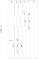
- FIG. 1 is a block diagram illustrating an embodiment of a driver
- FIG. 2 is a timing diagram for describing an operation of a driver of FIG. 1 .
- a driver 100 in embodiments may include a plurality of stages STG1, STG2, STG3, STG4, etc.
- the driver 100 may be implemented in the form of a shift register in which a plurality of stages STG1, STG2, STG3, STG4, etc. sequentially output output signals OUT1, OUT2, OUT3, OUT4, etc.
- the driver 100 may be included in a display device, and may be formed in a display panel of the display device. In an embodiment, the driver 100 may be integrated or formed on a substrate of the display panel, for example.
- the plurality of stages STG1, STG2, STG3, STG4, etc. may sequentially output the output signals OUT1, OUT2, OUT3, OUT4, etc. based on a start signal FLM, a clock signal CLK and an inverted clock signal CLKB. Further, a first stage STG1 may receive the start signal FLM as an input signal, and each of subsequent stages STG2, STG3, STG4, etc., may receive the output signal of a previous stage as the input signal.
- a second stage STG2 may receive a first output signal OUT1 of the first stage STG1 as the input signal
- a third stage STG3 may receive a second output signal OUT2 of the second stage STG2 as the input signal
- a fourth stage STG4 may receive a third output signal OUT3 of the third stage STG3 as the input signal, for example.
- each odd-numbered stage STG1, STG3, etc. may start outputting the output signal OUT1, OUT3, etc., when the clock signal CLK has a relatively high level
- each even-numbered stage STG2, STG4, etc. may start outputting the output signal OUT2, OUT4, etc., when the inverted clock signal CLKB has the relatively high level.
- the first stage STG1 may start outputting the first output signal OUT1 having the relatively high level, for example.
- the first stage STG1 may start outputting the first output signal OUT1 having the relatively low level.
- the second stage STG2 may start outputting the second output signal OUT2 having the relatively high level.
- the second stage STG2 may start outputting the second output signal OUT2 having the relatively low level.
- the third stage STG3 may start outputting the third output signal OUT3 having the relatively high level. Further, when the clock signal CLK becomes the relatively high level after the second output signal OUT2 becomes the relatively low level, the third stage STG3 may start outputting the third output signal OUT3 having the relatively low level.
- the fourth stage STG4 may start outputting the fourth output signal OUT4 having the relatively high level.
- the fourth stage STG4 may start outputting the fourth output signal OUT4 having the relatively low level.
- the plurality of stages STG1, STG2, STG3, STG4, etc. may sequentially output the output signals OUT1, OUT2, OUT3, OUT4, etc., by delaying or shifting the output signals OUT1, OUT2, OUT3, OUT4, etc., by half a period of the clock signal CLK.
- the relatively high level may be a logic high level and the relatively low level may be a logic low level, but the invention is not limited thereto.
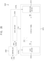
- FIG. 3 is a circuit diagram illustrating an embodiment of a stage of a driver
- FIG. 4 is a cross-sectional diagram illustrating an embodiment of a p-type metal-oxide-semiconductor ("PMOS") transistor and an n-type metal-oxide-semiconductor (“NMOS”) transistor included in the stage of FIG. 3 .
- PMOS metal-oxide-semiconductor
- NMOS n-type metal-oxide-semiconductor
- each stage STG of a driver in embodiments may include an input circuit INC that transfers an input signal SIN to a first node N1, and inverters INV1 and INV2 that generate an output signal OUT based on a voltage of the first node N1.
- the input circuit INC may transfer the input signal SIN to the first node N1 in response to at least one of a clock signal CLK and an inverted clock signal CLKB.
- the input circuit INC of a first stage among a plurality of stages of the driver may receive a start signal FLM as the input signal SIN, and each of subsequent stages may receive an output signal POUT of a previous stage as the input signal SIN.
- the input circuit INC of an odd-numbered stage may transfer the input signal SIN to the first node N1 when the clock signal CLK has a relatively high level and the inverted clock signal CLKB has a relatively low level
- the input circuit INC of an even-numbered stage may transfer the input signal SIN to the first node N1 when the clock signal CLK has the relatively low level and the inverted clock signal CLKB has the relatively high level
- the input circuit INC may be implemented as a CMOS transmission gate including a PMOS transistor and an NMOS transistor connected in parallel. In other embodiments, the input circuit INC may include only the PMOS transistor, or may include only the NMOS transistor.
- the stage STG may include an inverter chain including an even number of the inverters INV1 and INV2 connected in series.
- the stage STG may include two inverters INV1 and INV2.
- a first inverter INV1 may include an input terminal connected to the first node N1 and an output terminal connected to a second node N2, and may invert the voltage of the first node N1.
- a second inverter INV2 may include an input terminal connected to the second node N2 and an output terminal connected to an output node NO, and may invert a voltage of the second node N2 to generate the output signal OUT. Accordingly, the output signal OUT having a voltage corresponding to the voltage of the first node N1 may be output at the output node NO.
- At least one of the inverters INV1 and INV2 may include a PMOS transistor and an NMOS transistor connected in series between a line transferring a relatively high gate voltage and a line transferring a relatively low gate voltage.
- a first active region of the PMOS transistor may include or consist of materials different from materials of a second active region of the NMOS transistor.
- the NMOS transistor may include a top gate disposed above the second active region and a bottom gate disposed below the second active region.
- a first source/drain region SD1, the first active region ACT1 and a second source/drain region SD2 of the PMOS transistor PT may be formed on a substrate SUB of a display panel, for example.
- a buffer layer may be further formed between the substrate SUB and the first active region ACT1 to prevent impurities, but the invention is not limited thereto.
- the first active region ACT1 of the PMOS transistor PT may include or consist of polycrystalline silicon, e.g., relatively low temperature polycrystalline silicon ("LTPS").
- the first and second source/drain regions SD1 and SD2 may be p+ doped regions, and may serve as a source and a drain of the PMOS transistor PT, respectively.
- a first gate insulating layer GI1 may be formed on the first source/drain region SD1, the first active region ACT1 and the second source/drain region SD2.
- the first gate insulating layer GI1 may include or consist of silicon oxide, for example, but is not limited thereto.
- a gate GAT1 of the PMOS transistor PT may be formed on the first gate insulating layer (or film) GI1.
- the gate GAT1 of the PMOS transistor PT may include or consist of a metal material such as molybdenum, for example, but is not limited thereto.
- a second gate insulating layer GI2 may be formed on the gate GAT1 of the PMOS transistor PT.
- the second gate insulating layer GI2 may include or consist of silicon nitride, for example, but is not limited thereto.
- the bottom gate BML of the NMOS transistor NT may be formed on the second gate insulating layer (or film) GI2.
- the bottom gate BML may include or consist of a metal material such as molybdenum, for example, but is not limited thereto.
- a second relatively low gate voltage different from the relatively low gate voltage that is a relatively low voltage of the input signal SIN, the clock signal CLK, the inverted clock signal CLKB and the output signal OUT may be applied to the bottom gate BML of the NMOS transistor NT.
- the second relatively low gate voltage applied to the bottom gate BML may serve as a body bias voltage of the NMOS transistor NT, and a threshold voltage of the NMOS transistor NT may be adjusted by adjusting the second relatively low gate voltage.
- the second relatively low gate voltage lower than the relatively low gate voltage may be applied to the bottom gate BML, and thus the threshold voltage of the NMOS transistor NT may be increased, for example. In this case, a leakage current flowing through the NMOS transistor NT may be reduced.
- the bottom gate BML of the NMOS transistor NT may be connected to the top gate GAT2 of the NMOS transistor NT.
- a first inter-insulating layer ILD1 may be formed on the bottom gate BML.
- the first inter-insulating layer (or film) ILD1 may include or consist of silicon oxide or silicon nitride, for example, but is not limited thereto.
- a third source/drain region SD3, the second active region ACT2 and a fourth source/drain region SD4 of the NMOS transistor NT may be formed on the first inter-insulating layer ILD1.
- the second active region ACT2 of the NMOS transistor NT may include or consist of a material different from the material of the first active region ACT1 of the PMOS transistor PT.
- the second active region ACT2 of the NMOS transistor NT may include or consist of an oxide semiconductor, an organic semiconductor, amorphous silicon, etc., for example. That is, in some embodiments, the first active region ACT1 of the PMOS transistor PT may include polycrystalline silicon, and the second active region ACT2 of the NMOS transistor NT may include an oxide semiconductor.
- the first active region ACT1 of the PMOS transistor PT may include polycrystalline silicon
- the second active region ACT2 of the NMOS transistor NT may include an organic semiconductor.
- the first active region ACT1 of the PMOS transistor PT may include polycrystalline silicon
- the second active region ACT2 of the NMOS transistor NT may include amorphous silicon.
- the first active region ACT1 of the PMOS transistor PT and the second active region ACT2 of the NMOS transistor NT may be formed in different layers, respectively, disposed at different heights, respectively, from the substrate SUB of the display panel.
- the third and fourth source/drain regions SD3 and SD4 may be n+ doped regions, and may serve as a source and a drain of the NMOS transistor NT, respectively.
- a third gate insulating layer GI3 may be formed on the third source/drain region SD3, the second active region ACT2 and the fourth source/drain region SD4.
- the third gate insulating layer GI3 may include or consist of silicon nitride, but is not limited thereto.
- the top gate GAT2 of the NMOS transistor NT may be formed on the third gate insulating layer (or film) GI3, for example.
- the top gate GAT2 of the NMOS transistor NT may include or consist of a metal material such as molybdenum or titanium, for example, but is not limited thereto.
- a second inter-insulating layer ILD2 may be formed on the top gate GAT2 of the NMOS transistor NT.
- the second inter-insulating layer (or film) ILD2 may include or consist of silicon oxide or silicon nitride, for example, but is not limited thereto.
- Each stage of a conventional driver may include only a single type of transistor.
- each stage includes only a PMOS transistor, to output an output signal having a relatively low voltage level, a bootstrapping operation that decreases a voltage of an internal node of the stage to a voltage level lower than the relatively low voltage level should be performed, for example.
- a bootstrapping operation that increases a voltage of an internal node of the stage to a voltage level higher than the relatively high voltage level should be performed.
- At least one of the inverters INV1 and INV2 may include both of the PMOS transistor PT and the NMOS transistor NT, and the first active region ACT1 of the PMOS transistor PT may include or consist of materials different from materials of the second active region ACT2 of the NMOS transistor NT.
- the PMOS transistor PT may output the output signal OUT having the relatively high voltage level
- the NMOS transistor NT may output the output signal OUT having the relatively low voltage level. Accordingly, the bootstrapping operation may not be desired in the stage, and power consumption of the driver and a display device including the driver may be reduced.
- FIG. 5 is a circuit diagram illustrating an embodiment of a stage of a driver
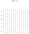
- FIG. 6 is a timing diagram for describing an embodiment of an operation of a stage of FIG. 5 .
- a stage 200 of a driver in embodiments may include an input circuit INC, a first inverter INV1 and a second inverter INV2.
- the stage 200 may further include a first capacitor C1 and/or a fourth PMOS transistor PT4.
- the input circuit INC may transfer an input signal SIN to a first node N1 in response to at least one of a clock signal CLK and an inverted clock signal CLKB.
- the input circuit INC may include a first PMOS transistor PT1 that transfers the input signal SIN to the first node N1 in response to the inverted clock signal CLKB.
- the input circuit INC may include a first NMOS transistor NT1 that transfers the input signal SIN to the first node N1 in response to the clock signal CLK.
- the input circuit INC may include the first PMOS transistor PT1 and the first NMOS transistor NT1 connected in parallel. That is, the input circuit INC may be implemented as a CMOS transmission gate.
- the first PMOS transistor PT1 may include a gate receiving the inverted clock signal CLKB, a first terminal receiving the input signal SIN, and a second terminal connected to the first node N1
- the first NMOS transistor NT1 may include a gate receiving the clock signal CLK, a first terminal receiving the input signal SIN, and a second terminal connected to the first node N1.
- the first PMOS transistor PT1 and the first NMOS transistor NT1 of the input circuit INC may be turned on to transfer the input signal SIN having the relatively high level to the first node N1.
- a voltage of the first node N1 may be changed to the relatively high level.
- FIGS. 5 and 6 illustrate an embodiment of the input circuit INC of an odd-numbered stage 200 that transfers the input signal SIN to the first node N1 when the clock signal CLK has the relatively high level and the inverted clock signal CLKB has the relatively low level.
- the input circuit INC of an even-numbered stage may transfer the input signal SIN to the first node N1 when the clock signal CLK has the relatively low level and the inverted clock signal CLKB has the relatively high level. That is, the first PMOS transistor PT1 of the input circuit INC of the even-numbered stage may receive the clock signal CLK, and the first NMOS transistor NT1 of the input circuit INC of the even-numbered stage may receive the inverted clock signal CLKB.
- the first capacitor C1 may hold the voltage of the first node N1 while the first PMOS transistor PT1 and the first NMOS transistor NT1 of the input circuit INC are turned off.
- the first capacitor C1 may be connected between a line transferring a relatively high gate voltage VGH and the first node N1. That is, the first capacitor C1 may include a first electrode connected to the line transferring the relatively high gate voltage VGH and a second electrode connected to the first node N1. In other embodiments, the first capacitor C1 may be connected between a line transferring a relatively low gate voltage VGL and the first node N1.
- the first inverter INV1 may be implemented as a first CMOS inverter including a second PMOS transistor PT2 and a second NMOS transistor NT2 connected in series between the line transferring the relatively high gate voltage VGH and the line transferring the relatively low gate voltage VGL.
- the second PMOS transistor PT2 may include a gate connected to the first node N1, a first terminal connected to the line transferring the relatively high gate voltage VGH, and a second terminal connected to a second node N2
- the second NMOS transistor NT2 may include a gate connected to the first node N1, a first terminal connected to the line transferring the relatively low gate voltage VGL, and a second terminal connected to the second node N2.
- the first inverter INV1 may provide an inverted voltage to the second node N2 by inverting the voltage of the first node N1.
- the first inverter INV1 may provide a voltage having the relatively low level to the second node N2 when the voltage of the first node N1 has the relatively high level, and may provide a voltage having the relatively high level to the second node N2 when the voltage of the first node N1 has the relatively low level, for example. That is, when the voltage of the first node N1 has the relatively high level, the second NMOS transistor NT2 may be turned on, and the second NMOS transistor NT2 may transfer the relatively low gate voltage VGL to the second node N2. Further, when the voltage of the first node N1 has the relatively low level, the second PMOS transistor PT2 may be turned on, and the second PMOS transistor PT2 may transfer the relatively high gate voltage VGH to the second node N2.
- the second inverter INV2 may be implemented as a second CMOS inverter including a third PMOS transistor PT3 and a third NMOS transistor NT3 connected in series between the line transferring the relatively high gate voltage VGH and the line transferring the relatively low gate voltage VGL.
- the third PMOS transistor PT3 may include a gate connected to the second node N2, a first terminal connected to the line transferring the relatively high gate voltage VGH, and a second terminal connected to an output node NO at which an output signal OUT is output
- the third NMOS transistor NT3 may include a gate connected to the second node N2, a first terminal connected to the line transferring the relatively low gate voltage VGL, and a second terminal connected to the output node NO.
- the second inverter INV2 may generate the output signal OUT by inverting a voltage of the second node N2.
- the second inverter INV2 may generate the output signal OUT having the relatively low level when the voltage of the second node N2 has the relatively high level, and may generate the output signal OUT having the relatively high level when the voltage of the second node N2 has the relatively low level, for example. That is, when the voltage of the second node N2 has the relatively high level, the third NMOS transistor NT3 may be turned on, and the third NMOS transistor NT3 may output the relatively low gate voltage VGL as the output signal OUT at the output node NO. Further, when the voltage of the second node N2 has the relatively low level, the third PMOS transistor PT3 may be turned on, and the third PMOS transistor PT3 may output the relatively high gate voltage VGH as the output signal OUT at the output node NO.
- the fourth PMOS transistor PT4 may transfer the relatively high gate voltage VGH to the first node N1 in response to a global reset signal ESR.
- the global reset signal ESR may have the relatively low level when a power-on sequence of a display device is performed, and may be substantially simultaneously provided to a plurality of stages of the driver.
- the fourth PMOS transistors PT4 of the plurality of stages may transfer the relatively high gate voltage VGH to the first nodes N1 of the plurality of stages during the power-on sequence, thereby stabilizing voltages of nodes N1, N2 and NO of the plurality of stages during the power-on sequence.
- the fourth PMOS transistor PT4 may include a gate receiving the global reset signal ESR, a first terminal connected to the line transferring the relatively high gate voltage VGH, and a second terminal connected to the first node N1.
- FIG. 5 illustrates an embodiment in which the fourth PMOS transistor PT4 is connected to the line transferring the relatively high gate voltage VGH, in other embodiments, the fourth PMOS transistor PT4 may be connected to the line transferring the relatively low gate voltage VGL. In this case, the fourth PMOS transistor PT4 may transfer the relatively low gate voltage VGL to the first node N1 during the power-on sequence.
- active regions of the first through fourth PMOS transistors PT1 through PT4 may include or consist of materials different from materials of active regions of the first through third NMOS transistors NT1 through NT3.
- the active regions of the first through fourth PMOS transistors PT1 through PT4 may include or consist of polycrystalline silicon
- the active regions of the first through third NMOS transistors NT1 through NT3 may include or consist of an oxide semiconductor, an organic semiconductor, amorphous silicon, etc., for example.
- each of the first through third NMOS transistors NT1 through NT3 may include a bottom gate, and the bottom gate may be connected to a line transferring a second relatively low gate voltage VGL2. That is, the second relatively low gate voltage VGL2 different from the relatively low gate voltage VGL may be applied to the bottom gate. Accordingly, by adjusting the second relatively low gate voltage VGL2, a threshold voltage of each of the first through third NMOS transistors NT1 through NT3 may be adjusted. In some embodiments, the second relatively low gate voltage VGL2 may be lower than the relatively low gate voltage VGL. In this case, the threshold voltage of each of the first through third NMOS transistors NT1 through NT3 may be increased, and thus a leakage current flowing through the first through third NMOS transistors NT1 through NT3 may be reduced.
- FIG. 7 is a circuit diagram illustrating an embodiment of a stage of a driver.
- a stage 300 of a driver in embodiments may include a first PMOS transistor PT1, a second PMOS transistor PT2, a third PMOS transistor PT3, a fourth PMOS transistor PT4, a first NMOS transistor NT1', a second NMOS transistor NT2', a third NMOS transistor NT3' and a first capacitor C1.
- the stage 300 of FIG. 7 may have substantially the same configuration and operation as a stage 200 of FIG. 5 , except that a bottom gate of each of the first through third NMOS transistors NT1' through NT3' may be connected to its top gate.
- the bottom gate of the first NMOS transistor NT1' may be connected to the top gate of the first NMOS transistor NT1'
- the bottom gate of the second NMOS transistor NT2' may be connected to the top gate of the second NMOS transistor NT2'
- the bottom gate of the third NMOS transistor NT3' may be connected to the top gate of the third NMOS transistor NT3'.
- each of the first through third NMOS transistors NT1' through NT3' when each of the first through third NMOS transistors NT1' through NT3' is turned on, each of the first through third NMOS transistors NT1' through NT3' may have an upper channel by the top gate and a lower channel by the bottom gate, and thus an on-current of each of the first through third NMOS transistors NT1' through NT3' may be increased.
- FIG. 8 is a circuit diagram illustrating an embodiment of a stage of a driver.
- a stage 400 of a driver in embodiments may include a first PMOS transistor PT1, a second PMOS transistor PT2, a third PMOS transistor PT3, a fourth PMOS transistor PT4, a first NMOS transistor NT1, a second NMOS transistor NT2, and a third NMOS transistor NT3.
- the stage 400 of FIG. 8 may have substantially the same configuration and operation as a stage 200 of FIG. 5 , except that the stage 400 may not include a first capacitor.
- the stage 400 may not include the first capacitor for holding a voltage of a first node N1.
- the first PMOS transistor PT1 and the first NMOS transistor NT1 of an input circuit are turned off, instead of the first capacitor, parasitic capacitors CP1, CP2, CP3 and CP4 of the second PMOS and NMOS transistors PT2 and NT2 may hold the voltage of the first node N1.
- a first parasitic capacitor CP1 between a gate and a source of the second PMOS transistor PT2, a second parasitic capacitor CP2 between the gate and a drain of the second PMOS transistor PT2, a third parasitic capacitor CP3 between a top gate and a drain of the second NMOS transistor NT2, and a fourth parasitic capacitor CP4 between the top gate and a source of the second NMOS transistor NT2 may hold the voltage of the first node N1, for example.
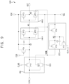
- FIG. 9 is a circuit diagram illustrating an embodiment of a stage of a driver
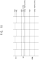
- FIG. 10 is a timing diagram for describing an embodiment of an operation of a charge pump circuit included in a stage of FIG. 9 .
- a stage 500 of a driver in embodiments may include an input circuit INC, a first inverter INV1, a second inverter INV2, a fourth PMOS transistor PT4, a first capacitor C1 and a charge pump circuit CPC.
- the stage 500 of FIG. 9 may have substantially the same configuration and operation as a stage 200 of FIG. 5 , except that the stage 500 may further include the charge pump circuit CPC.
- the stage 500 may not receive a second relatively low gate voltage applied to a bottom gate of each of first through third NMOS transistors NT1 through NT3, and the charge pump circuit CPC may generate a bottom gate voltage VBML applied to the bottom gate based on a relatively low gate voltage VGL and a clock signal CLK.
- the charge pump circuit CPC may include a fifth PMOS transistor PT5, a sixth PMOS transistor PT6, a second capacitor C2 and a seventh PMOS transistor PT7.
- the fifth PMOS transistor PT5 may include a gate connected to a third node N3, a first terminal connected to the bottom gate, and a second terminal connected to the third node N3.
- the sixth PMOS transistor PT6 may include a gate connected to a line transferring the relatively low gate voltage VGL, a first terminal connected to the third node N3, and a second terminal connected to the line transferring the relatively low gate voltage VGL.
- the second capacitor C2 may include a first electrode connected to the third node N3, and a second electrode.
- the seventh PMOS transistor PT7 may include a gate connected to the third node N3, a first terminal connected to the second electrode of the second capacitor C2, and a second terminal receiving the clock signal CLK.
- the sixth PMOS transistor PT6 may function as a diode that allows a current to flow only in a direction from the third node N3 to the line transferring the relatively low gate voltage VGL. Further, since the gate and the second terminal of the fifth PMOS transistor PT5 are connected to each other, the fifth PMOS transistor PT5 may function as a diode that allows a current to flow only in a direction from the bottom gate to the third node N3.
- a current may flow from the third node N3 from through the sixth PMOS transistor PT6 to the line transferring the relatively low gate voltage VGL, and thus the voltage of the third node N3 may become a sum VGL+
- the seventh PMOS transistor PT7 may transfer the relatively high gate voltage VGH to the second electrode of the second capacitor C2, and a voltage of the second electrode of the second capacitor C2 may become a voltage VGH-
- the voltage of the second electrode of the second capacitor C2 may be decreased by "VGH-VGL-
- a voltage of the third node N3 connected to the first electrode of the second capacitor C2 also may be decreased by "VGH-VGL-
- the voltage of the third node N3 may become "VGL+
- the bottom gate and the third node N3 may be electrically separated from each other when the voltage of the third node N3 is "VGL+
- the bottom gate voltage VBML may become a sum of the voltage of the third node N3 and an absolute value
- the relatively high gate voltage VGH is about 7 volts (V)
- the relatively low gate voltage VGL is about -8V
- of the threshold voltage of each of the fifth through seventh PMOS transistors PT5 through PT7 is about 2V
- the bottom gate voltage VBML may be "2 ⁇ (-8)-7+6" V, or about - 17V, which is lower than the relatively low gate voltage VGL, for example.
- a threshold voltage of the first through third NMOS transistors NT1 through NT3 may be increased, and leakage currents flowing through the first through third NMOS transistors NT1 through NT3 may be reduced.
- FIG. 11 is a circuit diagram illustrating an embodiment of a stage of a driver.
- a stage 600 of a driver in embodiments may include a first PMOS transistor PT1, a second PMOS transistor PT2, a third PMOS transistor PT3, a fourth PMOS transistor PT4, a first NMOS transistor NT1, a second NMOS transistor NT2, a third NMOS transistor NT3, a first capacitor C1 and an eighth PMOS transistor PT8.
- the stage 600 of FIG. 11 may have substantially the same configuration and operation as a stage 200 of FIG. 5 , except that the stage 600 may further include the eighth PMOS transistor PT8.
- the eighth PMOS transistor PT8 may transfer a relatively low gate voltage VGL to an output node NO in response to a voltage of a first node N1.
- the eighth PMOS transistor PT8 may be turned on when the third NMOS transistor NT3 is turned on, and may serve as a pull-down transistor for pulling down an output signal OUT to the relatively low gate voltage VGL along with the third NMOS transistor NT3. Accordingly, in the stage 600, the output signal OUT may rapidly fall from the relatively high gate voltage VGH to the relatively low gate voltage VGL, or may have a sharp falling edge.
- the eighth PMOS transistor PT8 may include a gate connected to the first node N1, a first terminal connected to an output node NO at which the output signal OUT is output, and a second terminal connected to a line transferring the relatively low gate voltage VGL.
- FIG. 12 is a circuit diagram illustrating an embodiment of a stage of a driver
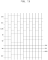
- FIG. 13 is a timing diagram for describing an embodiment of an operation of a stage of FIG. 12 .
- a stage 700 of a driver in embodiments may include an input circuit INC, a first inverter INV1, a second inverter INV2', a fourth PMOS transistor PT4, a first capacitor C1 and a PMOS boosting buffer PBB.
- the stage 700 of FIG. 12 may have substantially the same configuration and operation as a stage 200 of FIG. 5 , except that the second inverter INV2' is implemented as a PMOS inverter having only a third PMOS transistor PT3, and that the stage 700 may further include the PMOS boosting buffer PBB.
- the second inverter INV2' may output a relatively high gate voltage VGH as an output signal OUT.
- the PMOS boosting buffer PBB may output a relatively low gate voltage VGL as the output signal OUT.
- the PMOS boosting buffer PBB may include a third capacitor C3, a ninth PMOS transistor PT9 and a tenth PMOS transistor PT10.
- the third capacitor C3 may include a first electrode connected to an output node NO at which the output signal OUT is output, and a second electrode connected to a fourth node N4.
- the ninth PMOS transistor PT9 may include a gate connected to the fourth node N4, a first terminal connected to the output node NO, and a second terminal connected to a line transferring the relatively low gate voltage VGL.
- the tenth PMOS transistor PT10 may include a gate connected to the line transferring the relatively low gate voltage VGL, a first terminal connected to the first node N1, and a second terminal connected to the fourth node N4.
- the third PMOS transistor PT3 of the second inverter INV2' may be turned on, and the third PMOS transistor PT3 may transfer the relatively high gate voltage VGH to the output node NO. While the voltage of the first node N1 has the relatively high level, the tenth PMOS transistor PT 10 may transfer the voltage of the first node N1 having the relatively high level to the fourth node N4, and the voltage of the fourth node N4 may have the relatively high level.
- the tenth PMOS transistor PT10 may transfer the voltage of the first node N1 having the relatively low level to the fourth node N4, and the voltage of the fourth node N4 may have the relatively low level.
- the ninth PMOS transistor PT9 may transfer the relatively low gate voltage VGL to the output node NO, and the voltage of the output node NO may be decreased from the relatively high gate voltage VGH to the relatively low gate voltage VGL.
- the voltage of the output node NO connected to the first electrode of the third capacitor C3 is decreased, the voltage of the fourth node N4 connected to the second electrode of the third capacitor C3 also may be further decreased.
- An operation in which the voltage of the fourth node N4 is decreased to a boosted low gate voltage BVGL lower than the relatively low gate voltage VGL of the output node NO may be also referred to as a boosting operation.
- the voltage of the fourth node N4 may become a boosted low gate voltage BVGL is lower than the relatively low gate voltage VGL. Since the fourth node N4 has the boosted low gate voltage BVGL, the ninth PMOS transistor PT9 may be fully turned on, and the relatively low gate voltage VGL may be stably output as the output signal OUT at the output node NO.
- FIG. 14 is a circuit diagram illustrating an embodiment of a stage of a driver.
- a stage 800 of a driver in embodiments may include an input circuit INC, a first inverter INV1, a second inverter INV2, a fourth PMOS transistor PT4, a first capacitor C1 and a PMOS boosting buffer PBB.
- the stage 800 of FIG. 14 may have substantially the same configuration and operation as a stage 200 of FIG. 5 , except that the stage 800 may further include the PMOS boosting buffer PBB.
- the stage 800 of FIG. 14 may include a third NMOS transistor NT3 and the PMOS boosting buffer PBB to output the relatively low gate voltage VGL as the output signal OUT.
- a period in which the relatively low gate voltage VGL is output as the output signal OUT may be increased when a display device performs a relatively low frequency driving operation.
- a voltage of a fourth node N4 may be undesirably increased by a leakage current during the period, and thus a voltage of the output signal OUT may be undesirably increased during the period.
- the voltage of the output signal OUT may be substantially constant during the period.
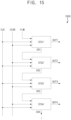
- FIG. 15 is a block diagram illustrating an embodiment of a driver
- FIG. 16 is a timing diagram for describing an operation of a driver of FIG. 15 .
- a driver 1000 in embodiments may include a plurality of stages STG1', STG2', STG3', STG4', etc.
- each stage may receive a carry signal of a previous stage as an input signal.
- a second stage STG2' may receive a first carry signal CR1 of a first stage STG1' as the input signal
- a third stage STG3' may receive a second carry signal CR2 of the second stage STG2' as the input signal
- a fourth stage STG4' may receive a third carry signal CR3 of the third stage STG3' as the input signal, for example.
- each odd-numbered stage STG1', STG3', etc. may start outputting a carry signal CR1, CR3, ... and an output signal OUT1, OUT3, etc., when a clock signal CLK has a relatively high level
- each even-numbered stage STG2', STG4', etc. may start outputting a carry signal CR2, CR4, ... and an output signal OUT2, OUT4, etc., when an inverted clock signal CLKB has the relatively high level.
- the first stage STG1' may start outputting the first carry signal CR1 having the relatively high level and a first output signal OUT1 having the relatively high level, for example. Further, when the clock signal CLK becomes the relatively high level after the start signal FLM becomes a relatively low level, the first stage STG1' may start outputting the first carry signal CR1 having the relatively low level and the first output signal OUT1 having the relatively low level.
- the second stage STG2' may start outputting the second carry signal CR2 having the relatively high level and a second output signal OUT2 having the relatively high level. Further, when the inverted clock signal CLKB becomes the relatively high level after the first carry signal CR1 becomes the relatively low level, the second stage STG2' may start outputting the second carry signal CR2 having the relatively low level and the second output signal OUT2 having the relatively low level.
- the fourth stage STG4' may start outputting a fourth carry signal CR4 having the relatively high level and a fourth output signal OUT4 having the relatively high level. Further, when the inverted clock signal CLKB becomes the relatively high level after the third carry signal CR3 becomes the relatively low level, the fourth stage STG4' may start outputting the fourth carry signal CR4 having the relatively low level and the fourth output signal OUT4 having the relatively low level. In this manner, the plurality of stages STG1', STG2', STG3', STG4', etc., may sequentially output the carry signals CR1, CR2, CR3, CR4, ...
- FIG. 17 is a circuit diagram illustrating an embodiment of a stage of a driver.
- a stage 1100 of a driver in embodiments may include an input circuit INC, a first inverter INV1, a second inverter INV2, a third inverter INV3, a fourth PMOS transistor PT4, a first capacitor C1 and a PMOS boosting buffer PBB.
- the stage 1100 of FIG. 17 may have substantially the same configuration and operation as a stage 800 of FIG. 14 , except that the stage 1100 may further include the third inverter INV3 for outputting a carry signal CR.
- the third inverter INV3 may generate the carry signal CR by inverting a voltage of a second node N2, and may be implemented as a CMOS inverter including an eleventh PMOS transistor PT11 and a fourth NMOS transistor NT4.
- the eleventh PMOS transistor PT11 may include a gate connected to the second node N2, a first terminal connected to a line transferring a relatively high gate voltage VGH, and a second terminal connected to a carry node NC at which the carry signal CR is output
- the fourth NMOS transistor NT4 may include a gate connected to the second node N2, a first terminal connected to a line transferring a relatively low gate voltage VGL, and a second terminal connected to the carry node NC.
- An output node NO at which an output signal OUT is output may have a relatively large load since the output node NO is connected to a line that is connected to pixels of a display panel, but the carry node NC at which the carry signal CR is output may have a relatively small load since the carry node NC is not connected to the line connected to the pixels of the display panel and is connected only to a next stage. Accordingly, in the stage 1100 where the output node NO and the carry node NC are separated from each other, even when the output signal OUT does not rapidly rise and fall, the carry signal CR may rapidly and sharply rise and fall.
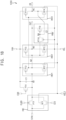
- FIG. 18 is a circuit diagram illustrating an embodiment of a stage of a driver.
- a stage 1200 of a driver in embodiments may include an input circuit INC, a first inverter INV1, a second inverter INV2, a third inverter INV3, a fourth PMOS transistor PT4, a first capacitor C1 and a PMOS boosting buffer PBB'.
- the stage 1200 of FIG. 18 may have substantially the same configuration and operation as a stage 1100 of FIG. 17 , except that a third capacitor C3' of the PMOS boosting buffer PBB' is connected to a carry node NC instead of an output node NO.
- the third capacitor C3' of the PMOS boosting buffer PBB' may be connected between a fourth node N4 and the carry node NC. That is, the third capacitor C3' may include a first electrode connected to the carry node NC at which a carry signal CR is output, and a second electrode connected to the fourth node N4. Since the carry node NC has a relatively small load compared with the output node NO, a boosting operation for the fourth node N3 by the third capacitor C3' may be relatively rapidly performed.
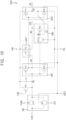
- FIG. 19 is a circuit diagram illustrating an embodiment of a stage of a driver.
- FIG. 20 is a block diagram illustrating an embodiment of a display device.
- a display device 2000 in embodiments may include a display panel 2010 that includes a plurality of pixels PX, a data driver 2030 that provides data signals DS to the plurality of pixels PX, a gate driver 2050 that provides gate signals GS to the plurality of pixels PX, an emission driver 2070 that provides emission signals EM to the plurality of pixels PX, and a controller 2090 that controls the data driver 2030, the gate driver 2050 and the emission driver 2070.
- the data driver 2030 may generate the data signals DS based on a data control signal DCTRL and output image data ODAT received from the controller 2090, and may provide the data signals DS to the plurality of pixels PX through the data lines.
- the data control signal DCTRL may include, but is not limited to, an output data enable signal, a horizontal start signal, and a load signal.
- the data driver 2030 and the controller 2090 may be implemented as a single integrated circuit, and the single integrated circuit may be referred to as a timing controller embedded data driver ("TED") integrated circuit. In other embodiments, the data driver 2030 and the controller 2090 may be implemented as separate integrated circuits.
- the gate driver 2050 may generate the gate signals GS based on a gate control signals GCTRL received from the controller 2090, and may sequentially provide the gate signals GS to the plurality of pixels PX through the gate lines on a row-by-row basis.
- the gate control signal GCTRL may include, but is not limited to, a gate start signal and a gate clock signal.
- the gate driver 2050 may be a driver 100 of FIG. 1 including a stage 200 of FIG. 5 , a stage 300 of FIG. 7 , a stage 400 of FIG. 8 , a stage 500 of FIG. 9 , a stage 600 of FIG. 11 , a stage 700 of FIG. 12 or a stage 800 of FIG.
- the gate driver 2050 may be integrated or formed in the display panel 2010. In other embodiments, the gate driver 2050 may be implemented as one or more integrated circuits.
- the emission driver 2070 may generate the emission signals EM based on an emission control signal ECTRL received from the controller 2090, and may sequentially provide the emission signals EM to the plurality of pixels PX through the emission lines on a row-by-row basis.
- the emission control signal ECTRL may include, but is not limited to, an emission start signal and an emission clock signal.
- the emission driver 2070 may have be the driver 100 of FIG. 1 including the stage 200 of FIG. 5 , the stage 300 of FIG. 7 , the stage 400 of FIG. 8 , the stage 500 of FIG. 9 , the stage 600 of FIG. 11 , the stage 700 of FIG. 12 or the stage 800 of FIG. 14 , or may be a driver 1000 of FIG.
- the emission driver 2070 may be integrated or formed in the display panel 2010. In other embodiments, the emission driver 2070 may be implemented as one or more integrated circuits.
- the controller 2090 may receive input image data IDAT and a control signal CTRL from an external host processor (e.g., a graphics processing unit (“GPU"), an application processor ("AP”) or a graphics card).
- an external host processor e.g., a graphics processing unit (“GPU"), an application processor ("AP") or a graphics card.
- the input image data IDAT may be RGB image data including red image data, green image data and blue image data.
- the control signal CTRL may include, but is not limited to, a vertical synchronization signal, a horizontal synchronization signal, an input data enable signal, a master clock signal, etc.
- the controller 2090 may generate the output image data ODAT, the data control signal DCTRL, the gate control signal GCTRL and the emission control signal ECTRL based on the input image data IDAT and the control signal CTRL.
- the controller 2090 may control an operation of the data driver 2030 by providing the output image data ODAT and the data control signal DCTRL to the data driver 2030, may control an operation of the gate driver 2050 by providing the gate control signal GCTRL to the gate driver 2050, and may control an operation of the emission driver 2070 by providing the emission control signal ECTRL to the emission driver 2070.
- At least one driver of the gate driver 2050 and the emission driver 2070 may be implemented as the driver 100 of FIG. 1 or the driver 1000 of FIG. 15 .
- At least one stage of the driver may include both of a PMOS transistor and an NMOS transistor, and an active region of the PMOS transistor may include or consist of materials different from materials of an active region of the NMOS transistor. Accordingly, a bootstrapping operation may not be desired in the stage, and power consumption of the driver and the display device 2000 may be reduced.
- FIG. 21 is a block diagram illustrating an embodiment of an electronic device including a display device.
- an electronic device 2100 may include a processor 2110, a memory device 2120, a storage device 2130, an input/output ("I/O") device 2140, a power supply 2150, and a display device 2160.
- the electronic device 2100 may further include a plurality of ports for communicating a video card, a sound card, a memory card, a universal serial bus (“USB”) device, other electric devices, etc.
- USB universal serial bus
- the processor 2110 may perform various computing functions or tasks.
- the processor 2110 may be an application processor ("AP"), a micro processor, a central processing unit (“CPU”), etc.
- the processor 2110 may be connected to other components via an address bus, a control bus, a data bus, etc. Further, in some embodiments, the processor 2110 may be further connected to an extended bus such as a peripheral component interconnection ("PCI”) bus.
- PCI peripheral component interconnection
- the memory device 2120 may store data for operations of the electronic device 2100.
- the memory device 2120 may include at least one non-volatile memory device such as an erasable programmable read-only memory (“EPROM”) device, an electrically erasable programmable read-only memory (“EEPROM”) device, a flash memory device, a phase change random access memory (“PRAM”) device, a resistance random access memory (“RRAM”) device, a nano floating gate memory (“NFGM”) device, a polymer random access memory (“PoRAM”) device, a magnetic random access memory (“MRAM”) device, a ferroelectric random access memory (“FRAM”) device, etc., and/or at least one volatile memory device such as a dynamic random access memory (“DRAM”) device, a static random access memory (“SRAM”) device, a mobile dynamic random access memory (“mobile DRAM”) device, etc., for example.
- DRAM dynamic random access memory
- SRAM static random access memory
- mobile DRAM mobile dynamic random access memory
- the storage device 2130 may be a solid state drive (“SSD”) device, a hard disk drive (“HDD”) device, a compact disc read-only memory (“CD-ROM”) device, etc.
- the I/O device 2140 may be an input device such as a keyboard, a keypad, a mouse, a touch screen, etc., and an output device such as a printer, a speaker, etc.
- the power supply 2150 may supply power for operations of the electronic device 2100.
- the display device 2160 may be connected to other components through the buses or other communication links.
- At least one stage may include both of a PMOS transistor and an NMOS transistor, and an active region of the PMOS transistor may include or consist of materials different from materials of an active region of the NMOS transistor. Accordingly, a bootstrapping operation may not be desired in the stage, and power consumption of the driver and the display device 2160 may be reduced.
- inventive concepts may be applied to any display device 2160 supporting the variable frame mode, and any electronic device 2100 including the display device 2160.
- inventive concepts may be applied to a smart phone, a wearable electronic device, a tablet computer, a mobile phone, a television ("TV”), a digital TV, a three dimensional ("3D") TV, a personal computer (“PC”), a home appliance, a laptop computer, a personal digital assistant (“PDA”), a portable multimedia player (“PMP”), a digital camera, a music player, a portable game console, a navigation device, etc., for example.
- TV television
- digital TV digital TV
- 3D three dimensional
- PC personal computer
- PDA personal digital assistant
- PMP portable multimedia player
- digital camera a music player
- portable game console a navigation device, etc.
Landscapes
- Engineering & Computer Science (AREA)
- Theoretical Computer Science (AREA)
- Physics & Mathematics (AREA)
- Computer Hardware Design (AREA)
- General Physics & Mathematics (AREA)
- Crystallography & Structural Chemistry (AREA)
- Chemical & Material Sciences (AREA)
- Logic Circuits (AREA)
- Control Of Indicators Other Than Cathode Ray Tubes (AREA)
- Microelectronics & Electronic Packaging (AREA)
- Metal-Oxide And Bipolar Metal-Oxide Semiconductor Integrated Circuits (AREA)
- Thin Film Transistor (AREA)
- Control Of El Displays (AREA)
Applications Claiming Priority (1)
| Application Number | Priority Date | Filing Date | Title |
|---|---|---|---|
| KR1020230062886A KR20240166065A (ko) | 2023-05-16 | 2023-05-16 | 드라이버 및 표시 장치 |
Publications (2)
| Publication Number | Publication Date |
|---|---|
| EP4465290A2 true EP4465290A2 (de) | 2024-11-20 |
| EP4465290A3 EP4465290A3 (de) | 2025-01-15 |
Family
ID=90361435
Family Applications (1)
| Application Number | Title | Priority Date | Filing Date |
|---|---|---|---|
| EP24161087.2A Pending EP4465290A3 (de) | 2023-05-16 | 2024-03-04 | Treiber und anzeigevorrichtung |
Country Status (4)
| Country | Link |
|---|---|
| US (2) | US12293695B2 (de) |
| EP (1) | EP4465290A3 (de) |
| KR (1) | KR20240166065A (de) |
| CN (1) | CN119007628A (de) |
Families Citing this family (1)
| Publication number | Priority date | Publication date | Assignee | Title |
|---|---|---|---|---|
| US20260024499A1 (en) * | 2024-07-19 | 2026-01-22 | Apple Inc. | Display Gate Driver Circuitry with Reduced Power Consumption and Smaller Footprint |
Family Cites Families (14)
| Publication number | Priority date | Publication date | Assignee | Title |
|---|---|---|---|---|
| JP2000132975A (ja) | 1998-08-21 | 2000-05-12 | Mitsubishi Electric Corp | 半導体装置およびそれを備えるメモリモジュ―ル |
| EP2016579A1 (de) * | 2006-09-05 | 2009-01-21 | Canon Kabushiki Kaisha | Organische lichtemittierende anzeigevorrichtung |
| CN103208251B (zh) | 2013-04-15 | 2015-07-29 | 京东方科技集团股份有限公司 | 一种移位寄存器单元、栅极驱动电路及显示装置 |
| KR102736793B1 (ko) | 2017-01-05 | 2024-12-04 | 삼성디스플레이 주식회사 | 주사 구동부 및 이를 포함하는 표시 장치 |
| KR102575564B1 (ko) | 2018-03-26 | 2023-09-08 | 삼성디스플레이 주식회사 | 주사 구동부 |
| US10825414B2 (en) | 2018-10-26 | 2020-11-03 | Sharp Kabushiki Kaisha | Scanning signal line drive circuit, display device provided with same, and drive method for scanning signal line |
| CN109872673B (zh) | 2019-04-09 | 2022-05-20 | 京东方科技集团股份有限公司 | 栅极驱动单元、栅极驱动方法、栅极驱动电路和显示装置 |
| KR102668997B1 (ko) | 2019-10-21 | 2024-05-24 | 삼성디스플레이 주식회사 | 표시 장치 |
| US11810920B2 (en) * | 2019-11-29 | 2023-11-07 | Samsung Electronics Co., Ltd. | Integrated circuits including integrated standard cell structure |
| US11735592B2 (en) * | 2019-12-20 | 2023-08-22 | Samsung Electronics Co., Ltd. | Integrated circuit including integrated standard cell structure |
| US11387817B2 (en) * | 2020-04-16 | 2022-07-12 | Samsung Electronics Co., Ltd. | Latch circuit, flip-flop circuit including the same |
| EP4123634B1 (de) | 2021-03-24 | 2025-05-14 | BOE Technology Group Co., Ltd. | Anzeigesubstrat und anzeigevorrichtung |
| WO2022252053A1 (zh) * | 2021-05-31 | 2022-12-08 | 京东方科技集团股份有限公司 | 行驱动信号增强电路、移位寄存器单元和显示面板 |
| US11979158B2 (en) * | 2022-02-23 | 2024-05-07 | Taiwan Semiconductor Manufacturing Company, Ltd. | Integrated circuit device, method and system |
-
2023
- 2023-05-16 KR KR1020230062886A patent/KR20240166065A/ko active Pending
-
2024
- 2024-01-03 US US18/403,346 patent/US12293695B2/en active Active
- 2024-03-04 EP EP24161087.2A patent/EP4465290A3/de active Pending
- 2024-03-19 CN CN202410310867.0A patent/CN119007628A/zh active Pending
-
2025
- 2025-04-10 US US19/175,206 patent/US20250239204A1/en active Pending
Also Published As
| Publication number | Publication date |
|---|---|
| US12293695B2 (en) | 2025-05-06 |
| EP4465290A3 (de) | 2025-01-15 |
| US20250239204A1 (en) | 2025-07-24 |
| US20240386838A1 (en) | 2024-11-21 |
| KR20240166065A (ko) | 2024-11-26 |
| CN119007628A (zh) | 2024-11-22 |
Similar Documents
| Publication | Publication Date | Title |
|---|---|---|
| US11694627B2 (en) | Scan driver and display device | |
| JP5332232B2 (ja) | 画素回路、デジタル駆動方式の電気光学装置および電子機器 | |
| US9190169B2 (en) | Shift register and flat panel display device having the same | |
| CN103534747B (zh) | 扫描信号线驱动电路、显示装置以及扫描信号线的驱动方法 | |
| US11410608B2 (en) | Shift register circuitry, gate driving circuit, display device, and driving method thereof | |
| WO2011114563A1 (ja) | シフトレジスタ | |
| US7800575B2 (en) | Display device | |
| CN114255701A (zh) | 移位寄存器单元及驱动方法、驱动电路和显示装置 | |
| CN114648947A (zh) | 扫描驱动器及其驱动方法 | |
| US20190108810A1 (en) | Shift register and display device provided with same | |
| CN109166542A (zh) | 移位寄存器单元及驱动方法、栅极驱动电路、显示装置 | |
| US12277885B2 (en) | Gate driver and display device including the same | |
| US20250239204A1 (en) | Driver and display device | |
| CN116264057A (zh) | 扫描驱动器和显示装置 | |
| CN100565711C (zh) | 移位寄存器电路及设有该电路的图像显示装置 | |
| JP7311427B2 (ja) | シフトレジスタ、ゲート駆動回路および表示装置 | |
| US12354531B2 (en) | Emission driver and display apparatus including the same | |
| US20250166551A1 (en) | Driver and display device | |
| US20250336323A1 (en) | Driver and display device | |
| US20250232733A1 (en) | Driver and display device | |
| US20250140198A1 (en) | Driver and display device | |
| US12603036B2 (en) | Driving circuit and display device | |
| EP4576054A1 (de) | Gate-treiber und anzeigevorrichtung damit | |
| US20140062572A1 (en) | Single input level shifter | |
| CN120431850A (zh) | 驱动器和包括该驱动器的显示设备 |
Legal Events
| Date | Code | Title | Description |
|---|---|---|---|
| PUAI | Public reference made under article 153(3) epc to a published international application that has entered the european phase |
Free format text: ORIGINAL CODE: 0009012 |
|
| STAA | Information on the status of an ep patent application or granted ep patent |
Free format text: STATUS: THE APPLICATION HAS BEEN PUBLISHED |
|
| AK | Designated contracting states |
Kind code of ref document: A2 Designated state(s): AL AT BE BG CH CY CZ DE DK EE ES FI FR GB GR HR HU IE IS IT LI LT LU LV MC ME MK MT NL NO PL PT RO RS SE SI SK SM TR |
|
| PUAL | Search report despatched |
Free format text: ORIGINAL CODE: 0009013 |
|
| AK | Designated contracting states |
Kind code of ref document: A3 Designated state(s): AL AT BE BG CH CY CZ DE DK EE ES FI FR GB GR HR HU IE IS IT LI LT LU LV MC ME MK MT NL NO PL PT RO RS SE SI SK SM TR |
|
| RIC1 | Information provided on ipc code assigned before grant |
Ipc: G09G 3/3266 20160101AFI20241210BHEP |
|
| STAA | Information on the status of an ep patent application or granted ep patent |
Free format text: STATUS: REQUEST FOR EXAMINATION WAS MADE |
|
| 17P | Request for examination filed |
Effective date: 20250317 |
|
| STAA | Information on the status of an ep patent application or granted ep patent |
Free format text: STATUS: EXAMINATION IS IN PROGRESS |
|
| 17Q | First examination report despatched |
Effective date: 20260128 |
|
| P01 | Opt-out of the competence of the unified patent court (upc) registered |
Free format text: CASE NUMBER: UPC_APP_0006948_4465290/2026 Effective date: 20260226 |