EP4439670A1 - Festkörperbildgebungsvorrichtung und verfahren zur herstellung einer festkörperbildgebungsvorrichtung - Google Patents
Festkörperbildgebungsvorrichtung und verfahren zur herstellung einer festkörperbildgebungsvorrichtung Download PDFInfo
- Publication number
- EP4439670A1 EP4439670A1 EP22898242.7A EP22898242A EP4439670A1 EP 4439670 A1 EP4439670 A1 EP 4439670A1 EP 22898242 A EP22898242 A EP 22898242A EP 4439670 A1 EP4439670 A1 EP 4439670A1
- Authority
- EP
- European Patent Office
- Prior art keywords
- solid
- transparent member
- imaging apparatus
- image sensor
- chip
- Prior art date
- Legal status (The legal status is an assumption and is not a legal conclusion. Google has not performed a legal analysis and makes no representation as to the accuracy of the status listed.)
- Withdrawn
Links
Images









Classifications
-
- H—ELECTRICITY
- H10—SEMICONDUCTOR DEVICES; ELECTRIC SOLID-STATE DEVICES NOT OTHERWISE PROVIDED FOR
- H10F—INORGANIC SEMICONDUCTOR DEVICES SENSITIVE TO INFRARED RADIATION, LIGHT, ELECTROMAGNETIC RADIATION OF SHORTER WAVELENGTH OR CORPUSCULAR RADIATION
- H10F39/00—Integrated devices, or assemblies of multiple devices, comprising at least one element covered by group H10F30/00, e.g. radiation detectors comprising photodiode arrays
- H10F39/80—Constructional details of image sensors
- H10F39/804—Containers or encapsulations
-
- H—ELECTRICITY
- H10—SEMICONDUCTOR DEVICES; ELECTRIC SOLID-STATE DEVICES NOT OTHERWISE PROVIDED FOR
- H10F—INORGANIC SEMICONDUCTOR DEVICES SENSITIVE TO INFRARED RADIATION, LIGHT, ELECTROMAGNETIC RADIATION OF SHORTER WAVELENGTH OR CORPUSCULAR RADIATION
- H10F39/00—Integrated devices, or assemblies of multiple devices, comprising at least one element covered by group H10F30/00, e.g. radiation detectors comprising photodiode arrays
- H10F39/011—Manufacture or treatment of image sensors covered by group H10F39/12
- H10F39/024—Manufacture or treatment of image sensors covered by group H10F39/12 of coatings or optical elements
-
- H—ELECTRICITY
- H10—SEMICONDUCTOR DEVICES; ELECTRIC SOLID-STATE DEVICES NOT OTHERWISE PROVIDED FOR
- H10F—INORGANIC SEMICONDUCTOR DEVICES SENSITIVE TO INFRARED RADIATION, LIGHT, ELECTROMAGNETIC RADIATION OF SHORTER WAVELENGTH OR CORPUSCULAR RADIATION
- H10F39/00—Integrated devices, or assemblies of multiple devices, comprising at least one element covered by group H10F30/00, e.g. radiation detectors comprising photodiode arrays
- H10F39/10—Integrated devices
- H10F39/12—Image sensors
- H10F39/199—Back-illuminated image sensors
-
- H—ELECTRICITY
- H10—SEMICONDUCTOR DEVICES; ELECTRIC SOLID-STATE DEVICES NOT OTHERWISE PROVIDED FOR
- H10F—INORGANIC SEMICONDUCTOR DEVICES SENSITIVE TO INFRARED RADIATION, LIGHT, ELECTROMAGNETIC RADIATION OF SHORTER WAVELENGTH OR CORPUSCULAR RADIATION
- H10F39/00—Integrated devices, or assemblies of multiple devices, comprising at least one element covered by group H10F30/00, e.g. radiation detectors comprising photodiode arrays
- H10F39/80—Constructional details of image sensors
- H10F39/805—Coatings
-
- H—ELECTRICITY
- H10—SEMICONDUCTOR DEVICES; ELECTRIC SOLID-STATE DEVICES NOT OTHERWISE PROVIDED FOR
- H10F—INORGANIC SEMICONDUCTOR DEVICES SENSITIVE TO INFRARED RADIATION, LIGHT, ELECTROMAGNETIC RADIATION OF SHORTER WAVELENGTH OR CORPUSCULAR RADIATION
- H10F39/00—Integrated devices, or assemblies of multiple devices, comprising at least one element covered by group H10F30/00, e.g. radiation detectors comprising photodiode arrays
- H10F39/80—Constructional details of image sensors
- H10F39/805—Coatings
- H10F39/8053—Colour filters
-
- H—ELECTRICITY
- H10—SEMICONDUCTOR DEVICES; ELECTRIC SOLID-STATE DEVICES NOT OTHERWISE PROVIDED FOR
- H10F—INORGANIC SEMICONDUCTOR DEVICES SENSITIVE TO INFRARED RADIATION, LIGHT, ELECTROMAGNETIC RADIATION OF SHORTER WAVELENGTH OR CORPUSCULAR RADIATION
- H10F39/00—Integrated devices, or assemblies of multiple devices, comprising at least one element covered by group H10F30/00, e.g. radiation detectors comprising photodiode arrays
- H10F39/80—Constructional details of image sensors
- H10F39/806—Optical elements or arrangements associated with the image sensors
-
- H—ELECTRICITY
- H10—SEMICONDUCTOR DEVICES; ELECTRIC SOLID-STATE DEVICES NOT OTHERWISE PROVIDED FOR
- H10F—INORGANIC SEMICONDUCTOR DEVICES SENSITIVE TO INFRARED RADIATION, LIGHT, ELECTROMAGNETIC RADIATION OF SHORTER WAVELENGTH OR CORPUSCULAR RADIATION
- H10F39/00—Integrated devices, or assemblies of multiple devices, comprising at least one element covered by group H10F30/00, e.g. radiation detectors comprising photodiode arrays
- H10F39/80—Constructional details of image sensors
- H10F39/811—Interconnections
-
- H—ELECTRICITY
- H10—SEMICONDUCTOR DEVICES; ELECTRIC SOLID-STATE DEVICES NOT OTHERWISE PROVIDED FOR
- H10F—INORGANIC SEMICONDUCTOR DEVICES SENSITIVE TO INFRARED RADIATION, LIGHT, ELECTROMAGNETIC RADIATION OF SHORTER WAVELENGTH OR CORPUSCULAR RADIATION
- H10F39/00—Integrated devices, or assemblies of multiple devices, comprising at least one element covered by group H10F30/00, e.g. radiation detectors comprising photodiode arrays
- H10F39/80—Constructional details of image sensors
- H10F39/806—Optical elements or arrangements associated with the image sensors
- H10F39/8063—Microlenses
Definitions
- the present technology relates to a solid-state imaging apparatus and a method of producing the solid-state imaging apparatus.
- the present technology relates to packaging of the solid-state imaging apparatus.
- a chip size package in which a light-receiving surface of a solid-state image sensor chip is hermetically sealed and an external connection terminal is drawn out from the back surface has been proposed.
- a chip size package a configuration in which a sealing member obtained by adhering a frame portion to a flat plate portion is adhered to a front surface of a solid-state image sensor chip has been disclosed (see, for example, Patent Literatures 1 and 2).
- an adhesive is used to adhere the sealing member obtained by adhering a frame portion to a flat plate portion to the solid-state image sensor chip. For this reason, the number of joint surfaces between the sealing member and the solid-state image sensor chip increases, which may reduce the reliability of the solid-state imaging apparatus.
- the present technology has been made in view of such circumstances, and an object thereof is to improve reliability of a solid-state imaging apparatus.
- the present technology has been made to achieve the above-mentioned object, and a first aspect thereof is a solid-state imaging apparatus, including: a chip on which a solid-state image sensor is formed; and a transparent member that is directly joined to the chip via a projecting portion of the transparent member, the projecting portion maintaining a gap between the transparent member and an imaging region of the solid-state image sensor. This brings about the effect of increasing the joint strength between the chip and the transparent member.
- a joint between the chip and the transparent member may have a single joint interface. This brings about the effect that the transparent member is directly joined to the chip.
- the transparent member may be directly joined to a peripheral portion of the imaging region via the projecting portion such that a hollow portion is formed on the imaging region. This brings about the effect that the imaging region is sealed while preventing the chip and the transparent member from coming into contact with each other on the imaging region.
- the solid-state image sensor may be a back-illuminated solid-state image sensor. This brings about the effect that the wire is drawn out from the surface of the solid-state image sensor opposite to the imaging region.
- the transparent member may be a glass substrate on which the projecting portion is provided. This brings about the effect that inorganic matters are directly joined to each other.
- a coefficient of thermal expansion of glass of the glass substrate may be within a range of 2.4 to 3.5 ppm/°C. This brings about the effect that the difference in coefficient of thermal expansion between the transparent member and the chip is reduced.
- the chip may include a back-surface wire formed on a surface opposite to a surface on which the imaging region is formed, and a through electrode that penetrates the chip and is connected to the back-surface wire. This brings about the effect that the wire is drawn out from the back surface side of the chip where the imaging region is formed.
- the chip may include a semiconductor substrate on which the imaging region is provided, an anti-reflection film formed on the semiconductor substrate, a protective film formed on the anti-reflection film, a color filter formed on the protective film of the imaging region, and an on-chip lens formed on the color filter of the imaging region, and the transparent member may be directly joined to the protective film of a peripheral portion of the imaging region via the projecting portion.
- the chip may include a semiconductor substrate on which the imaging region is provided, an anti-reflection film formed on the semiconductor substrate, a protective film formed on the anti-reflection film of the imaging region, a color filter formed on the protective film of the imaging region, and an on-chip lens formed on the color filter of the imaging region, and the transparent member may be directly joined to the antireflection film of a peripheral portion of the imaging region via the projecting portion. This brings about the effect that light reflection caused by the difference in refractive index between the protective film and the transparent member is suppressed while improving the joint strength between the chip and the transparent member.
- the chip may include a semiconductor substrate on which the imaging region is provided, an anti-reflection film formed on the semiconductor substrate of the imaging region, a protective film formed on the anti-reflection film of the imaging region, a color filter formed on the protective film of the imaging region, and an on-chip lens formed on the color filter of the imaging region, and the transparent member may be directly joined to the semiconductor substrate of a peripheral portion of the imaging region via the projecting portion. This brings about the effect that the chip and the transparent member is directly joined to each other without interposing the protective film and the anti-reflection film.
- the first aspect may further include an inorganic film that is provided on a front surface of the projecting portion and is formed of a material different from that of the transparent member. This brings about the effect of optimizing the joint strength, the difference in coefficient of thermal expansion, and the difference in refractive index between the chip and the transparent member.
- the material of the inorganic film may be SiN, SiCN, or SiO 2 . This brings about the effect of optimizing the material to be used for direct joining between the chip and the transparent member.
- a bottom surface of a recessed portion surrounded by the projecting portion may have a curvature or a pattern having an optical function. This brings about the effect that the transparent member has a light collection function.
- the first aspect may further include an antireflection film formed on a surface of the transparent member other than a light incident path to the imaging region. This brings about the effect that the transparent member has a light collection function, which suppresses stray light and a decrease in sensitivity due to reflection of light that has entered the transparent member.
- a side surface of a recessed portion surrounded by the projecting portion may have a structure that scatters incident light. This brings about the effect reducing flare due to stray light.
- the transparent member may include a step that is located on an outer side surface of the projecting portion to separate a tip of the projecting portion from an end portion of the chip. This brings about the effect of suppressing the occurrence of cracks and chipping in the vicinity of the joint surface between the chip and the transparent member when performing separation into pieces by blade dicing.
- the first aspect may further include at least one of a first groove provided along an outer periphery of the chip or a second groove that connects the hollow portion to an outside of the transparent member on at least one of a joint surface on a side of the projecting portion or a joint surface on a side of the chip.
- the second groove may have a width of less than 5 ⁇ m and a depth of less than 1 ⁇ m. This brings about the effect of preventing moisture from entering during a cleaning step or the like while allowing the released gas to escape via the second groove.
- a second aspect is a method of producing a solid-state imaging apparatus, including:
- the step of directly joining may include a step of activating at least one of a joint surface on a side of the chip or a joint surface on a side of the transparent member, and a step of crimping the joint surface on the side of the chip and the joint surface on the side of the transparent member at a temperature of 250°C or less. This brings about the effect of increasing the joint strength between the chip and the transparent member while suppressing damage to the chip.
- Embodiments for carrying out the present technology (hereinafter, referred to as embodiments) will be described below. Description will be made in the following order.
- Fig. 1 is a diagram showing a configuration example of a solid-state imaging apparatus according to a first embodiment. Note that Part a in the figure is a cross-sectional view showing a configuration example of a solid-state imaging apparatus 100, and Part b in the figure is a plan view showing a configuration example of a joint region RC of a protective film 104.
- the solid-state imaging apparatus 100 includes a solid-state image sensor chip 101 and a transparent member 121.
- a solid-state image sensor is formed in the solid-state image sensor chip 101.
- the solid-state image sensor is, for example, a back-illuminated solid-state image sensor.
- the solid-state image sensor may be a CMOS (Complementary Metal Oxide Semiconductor) image sensor or a CCD (Charge Coupled Device) image sensor.
- CMOS Complementary Metal Oxide Semiconductor
- CCD Charge Coupled Device
- the solid-state image sensor chip 101 includes a semiconductor substrate 102 in which an imaging region RA and a non-imaging region RB are provided.
- the semiconductor substrate 102 is, for example, a single crystal silicon substrate.
- the semiconductor substrate 102 may be a group III-V substrate such as GaAs.
- the imaging region RA pixels and pixel transistors are arranged in a matrix along the row direction and the column direction.
- the non-imaging region RB peripheral circuits that drive the pixel transistors and output signals read from the pixels are provided.
- the imaging region RA is provided on the back surface side of the semiconductor substrate 102.
- an anti-reflection film 103 is formed on the semiconductor substrate 102.
- the protective film 104 is formed on the anti-reflection film 103.
- an inorganic matter such as SiO 2 and SiN can be used.
- a color filter 105 is formed on the protective film 104 for each pixel.
- the color filters 105 can form, for example, a Bayer array.
- a transparent resin to which a coloring agent is added can be used.
- an on-chip lens 106 is formed for each pixel.
- a transparent resin such as acrylic and polycarbonate can be used.
- a wiring layer 107 is formed on the semiconductor substrate 102.
- a wire embedded in an insulation layer is provided in the wiring layer 107.
- a land electrode 108 to which a through electrode 110 is connected can be formed in the wiring layer 107.
- the material of the insulation layer for example, SiO 2 can be used.
- a metal such as Al and Cu can be used.
- a support substrate 109 is attached onto the wiring layer 107.
- As the material of the support substrate 109 for example, Si or glass can be used.
- the thickness of the support substrate 109 can be made larger than that of the semiconductor substrate 102.
- the through electrode 110 is embedded in the support substrate 109 via a back-surface insulation film 111.
- the through electrode 110 penetrates the support substrate 109 in the thickness direction and is connected to the land electrode 108.
- a back-surface wire 112 is formed via the back-surface insulation film 111.
- a back-surface protective film 113 is formed on the back-surface wire 112.
- the materials of the through electrode 110 and the back-surface wire 112 for example, a metal such as Cu, Ti, Ta, Al, W, Ni, Ru, and Co can be used, and a stacked structure of a plurality of materials may be used.
- a metal such as Cu, Ti, Ta, Al, W, Ni, Ru, and Co
- a stacked structure of a plurality of materials may be used.
- the material of the back-surface insulation film 111 for example, SiO 2 , SiON, SiN, SiOC, or SiCN can be used when it is an inorganic film. When it is an organic film, a resin having a skeleton of silicone, polyimide, acrylic, epoxy, or the like can be used.
- a solder resist can be used as the material of the back-surface protective film 113.
- a protruding electrode 114 is connected to the back-surface wire 112. At this time, the back-surface protective film 113 is removed at the connection position between the back-surface wire 112 and the protruding electrode 114, and the back-surface wire 112 is exposed from the back-surface protective film 113.
- the protruding electrode 114 can be used as an external connection terminal for connecting the solid-state image sensor chip 101 to a motherboard or the like.
- the protruding electrode 114 may be, for example, a ball electrode such as a solder ball, or a pillar electrode formed of a conductor.
- the transparent member 121 includes a projecting portion 122.
- the projecting portion 122 can be formed along the periphery of the transparent member 121.
- the projecting portion 122 is integrated with the transparent member 121.
- the transparent member 121 and the projecting portion 122 can be integrally formed of the same material.
- the transparent member 121 on which the projecting portion 122 is provided can be formed on the basis of processing of a base material including a single material. At this time, there is no interface between the transparent member 121 and the projecting portion 122.
- the shape of the side surface of the projecting portion 122 may be vertical or may have a slight taper angle.
- an inorganic matter such as glass and quartz can be used.
- a transparent substrate on which the projecting portion 122 is provided may be used.
- CTE coefficient of thermal expansion
- the material of the protective film 104 is SiO 2
- the material of the protective film 104 is SiN
- An antireflection structure, a wafer-level lens, or the like may be stacked on the transparent member 121.
- the transparent member 121 is directly joined to the solid-state image sensor chip 101 via the projecting portion 122.
- the transparent member 121 is directly joined to a peripheral portion of the imaging region RA via the projecting portion 122 such that a hollow portion 123 is formed on the imaging region RA.
- the projecting portion 122 is formed such that a gap between the imaging region RA of the solid-state image sensor and the transparent member 121 is maintained. It is favorable to set the height of the projecting portion of the transparent member 121 to be within the range of 2 to 30 ⁇ m.
- the direct joining may be a method of pressurejoining at a temperature of 250°C or less while the plasma activation of the joint surface is performed.
- oxygen plasma or nitrogen plasma can be applied to the joint surface to perform hydrophilic treatment on the joint surface. Then, the joint surfaces can be in close contact with each other on the basis of the hydrogen bonds between OH groups formed on the joint surfaces due to the adsorption of moisture in the air. Then, the OH groups are decomposed by heat treatment, the hydrogens generated at that time are diffused into the interface layer, and thus, the direct joining based on the Si-O-Si bond via oxygen can be realized.
- the joint region RC is provided in the non-imaging region RB of the solid-state image sensor chip 101. Further, in the joint region RC, the color filter 105 and the on-chip lens 106 are not disposed and the protective film 104 is exposed. Then, by crimping the tip of the projecting portion 122 to the protective film 104 of the joint region RC, it is possible to directly join the transparent member 121 to the solid-state image sensor chip 101 while forming the hollow portion 123 on the imaging region RA. At this time, a single joint interface is formed between the solid-state image sensor chip 101 and the transparent member 121.
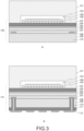
- Fig. 2 and Fig. 3 are each a cross-sectional view showing an example of a method of producing the solid-state imaging apparatus according to the first embodiment.
- a transparent substrate wafer 141 is prepared.
- the thickness of the transparent substrate wafer 141 can be set to, for example, approximately 50 to 1000 ⁇ m.
- a protective film or the like may be formed on the back surface side of the transparent substrate wafer 141. In the case where a protective film is formed on the back surface side of the transparent substrate wafer, it can be removed in the final step.
- the front surface side of the transparent substrate wafer 141 is processed by lithography and dry etching to form the projecting portion 122 on the front surface side of the transparent substrate wafer 141.
- the dry etching may be, for example, plasma etching or RIE (Reactive Ion Etching).
- the damaged layer may be removed by wet etching or the like.
- the projecting portion 122 is formed on the transparent substrate wafer 141 on the basis of processing of the transparent substrate wafer 141. This eliminates the necessity to adhere the projecting portion 122 to the transparent member 121 in order to provide the projecting portion 122 on the transparent member 121 shown in Fig. 1 , and makes it possible to form the transparent member 121 and the projecting portion 122 using the same material. Therefore, it is possible to suppress the complication of the step of producing the transparent member 121 on which the projecting portion 122 is provided and suppress a decrease in reliability due to thermal stress.
- the solid-state image sensor wafer 130 is prepared.
- the solid-state image sensor wafer 130 is a wafer before forming the through electrode 110 and the back-surface wire 112 shown in Fig. 1 .
- at least one of the front surface of the projecting portion 122 of the transparent substrate wafer 141 or the front surface of the protective film 104 of the solid-state image sensor wafer 130 is activated by plasma treatment.
- the transparent substrate wafer 141 and the solid-state image sensor wafer 130 are directly joined to each other.
- the coefficient of thermal expansion of the transparent substrate wafer 141 and the coefficient of thermal expansion of the protective film 104 may be caused to match.
- the crimping temperature of the direct joining it is possible to suppress the damage to the color filter 105.
- the damage to the color filter 105 is small even if the crimping temperature of the direct joining exceeds 200°C. For this reason, the crimping temperature of the direct joining only needs to be 250°C or less.
- a solid-state image sensor wafer 131 in which the through electrode 110 and the back-surface wire 112 are provided is formed on the back surface side of the solid-state image sensor wafer 130. Note that although a via-last process is taken in Part b of Fig. 3 , a via-middle process may be used.
- the back-surface protective film 113 and the protruding electrode 114 are formed on the back surface side of the solid-state image sensor wafer 131. Then, by separating the solid-state image sensor wafer 131 to which the transparent substrate wafer 141 is directly joined into chips by a method such as dicing, the solid-state imaging apparatus 100 in which the transparent member 121 is directly joined to the solid-state image sensor chip 101 is formed.
- the hollow portion 123 can be formed on the imaging region RA. Therefore, it is possible to seal the imaging region RA while preventing the solid-state image sensor chip 101 and the transparent member 121 from coming into contact with each other on the imaging region RA, and improve the reliability without deteriorating the optical performance of the solid-state imaging apparatus 100.
- a back-illuminated solid-state image sensor is used as a solid-state image sensor.
- a back-illuminated solid-state image sensor is used as a solid-state image sensor.
- the transparent member 121 a glass substrate on which the projecting portion 122 is provided, it is possible to directly join the inorganic matters to each other. Therefore, it is possible to improve the joint strength between the solid-state image sensor chip 101 and the transparent member 121, and suppress light reflection caused by the difference in refractive index on the joint surface while reducing stress caused by the difference in coefficient of thermal expansion on the joint surface. As a result, it is possible to improve the reliability of the solid-state imaging apparatus 100 while dealing with a decrease in joining area due to the miniaturization of the solid-state imaging apparatus 100, and directly join the solid-state image sensor chip 101 and the transparent member 121 to each other while suppressing an increase in the number of steps.
- the coefficient of thermal expansion of the glass substrate used for the transparent member 121 to be within the range of 2.4 to 3.5 ppm/°C, it is possible to reduce the difference in coefficient of thermal expansion between the solid-state image sensor chip 101 and the transparent member 121. Therefore, it is possible to reduce the stress caused by the difference in coefficient of thermal expansion between the solid-state image sensor chip 101 and the transparent member 121, and suppress warping of the solid-state image sensor chip 101.
- the transparent member 121 is directly joined to the protective film 104 of the joint region RC via the projecting portion 122 while the color filter 105 and the on-chip lens 106 of the peripheral portion of the imaging region RA are not disposed.
- the joint members using the same material. Therefore, it is possible to improve the joint strength by direct joining, and prevent light reflection caused by the difference in refractive index on the joint surface without generating stress caused by the difference in coefficient of thermal expansion on the joint surface.
- the back-surface wire 112 is provided on the back surface side of the solid-state image sensor chip 101, and the through electrode 110 that penetrates the solid-state image sensor chip 101 is provided. This eliminates the necessity to draw out the wire from the front surface side of the solid-state image sensor chip 101 in which the imaging region RA is formed, and makes it possible to increase the exclusive area of the imaging region RA on the front surface side of the solid-state image sensor chip 101.
- the transparent substrate wafer 141 is directly joined to the solid-state image sensor wafer 130, and then separated into chips by a method such as dicing.
- a method such as dicing.
- the transparent substrate wafer 141 including the projecting portion 122 may be formed on the basis of a glass mold.
- the transparent member 121 is directly joined to the protective film 104 of the solid-state image sensor chip 101 in the above-mentioned first embodiment, the transparent member 121 is directly joined to the anti-reflection film 103 in this second embodiment.
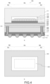
- Fig. 4 is a diagram showing a configuration example of a solid-state imaging apparatus according to the second embodiment. Note that Part a of Fig. 4 is a cross-sectional view showing a configuration example of a solid-state imaging apparatus 150, and Part b of Fig. 4 is a plan view showing a configuration example of the joint region RC of the anti-reflection film 103.
- a solid-state image sensor chip 151 and a transparent member 171 are provided instead of the solid-state image sensor chip 101 and the transparent member 121 in the above-mentioned first embodiment.
- a protective film 154 is provided instead of the protective film 104 in the above-mentioned first embodiment.
- the other configurations of the solid-state image sensor chip 151 are the same as the configurations of the solid-state image sensor chip 101 in the above-mentioned first embodiment.
- the protective film 154 is not disposed and the anti-reflection film 103 is exposed from the protective film 154.
- the other configurations of the protective film 154 are the same as the configurations of the protective film 104 in the above-mentioned first embodiment.
- a projecting portion 172 is provided instead of the projecting portion 122 in the above-mentioned first embodiment.
- the other configurations of the transparent member 171 are the same as the configurations of the transparent member 121 in the above-mentioned first embodiment.
- the transparent member 171 is directly joined to the solid-state image sensor chip 151 via the projecting portion 172. At this time, the tip of the projecting portion 172 is directly joined to the anti-reflection film 103 of the joint region RC.
- the transparent member 171 is directly joined to the anti-reflection film 103 exposed from the protective film 154.
- the transparent member 171 is directly joined to the anti-reflection film 103 exposed from the protective film 154.
- the transparent member 121 has been directly joined to the protective film 104 of the solid-state image sensor chip 101 in the above-mentioned first embodiment, the transparent member 121 is directly joined to the semiconductor substrate 102 in this third embodiment.
- Fig. 5 is a diagram showing a configuration example of a solid-state imaging apparatus according to a third embodiment. Note that Part a of Fig. 5 a cross-sectional view showing a configuration example of a solid-state imaging apparatus 200, and Part b of Fig. 5 is a plan view showing a configuration example of the joint region RC of the semiconductor substrate 102.
- a solid-state image sensor chip 201 and a transparent member 221 are provided instead of the solid-state image sensor chip 151 and the transparent member 171 in the above-mentioned second embodiment.
- an antireflection film 203 is provided instead of the anti-reflection film 103 in the above-mentioned second embodiment.
- the other configurations of the solid-state image sensor chip 201 are the same as the configurations of the solid-state image sensor chip 151 in the above-mentioned second embodiment.
- the anti-reflection film 203 is not disposed and the semiconductor substrate 102 is exposed from the antireflection film 203.
- the other configurations of the anti-reflection film 203 are the same as the configurations of the anti-reflection film 103 in the above-mentioned second embodiment.
- a projecting portion 222 is provided instead of the projecting portion 172 of the above-mentioned second embodiment.
- the other configurations of the transparent member 221 are the same as the configurations of the transparent member 171 in the above-mentioned second embodiment.
- the transparent member 221 is directly joined to the solid-state image sensor chip 201 via the projecting portion 222. At this time, the tip of the projecting portion 222 is directly joined to the semiconductor substrate 102 of the joint region RC.
- the transparent member 221 is directly joined to the semiconductor substrate 102 exposed from the protective film 154 and the anti-reflection film 103.
- the transparent member 121 is directly joined to the protective film 104 of the solid-state image sensor chip 101 in the above-mentioned first embodiment, the transparent member 121 is directly joined to the protective film 104 via an inorganic film 252 provided in the transparent member 121 in this fourth embodiment.
- This solid-state imaging apparatus is different from the solid-state imaging apparatus according to the first embodiment in that the inorganic film formed of a material different from that of the transparent member is interposed between the solid-state image sensor chip and the transparent member.
- Fig. 6 is a cross-sectional view showing a configuration example of the solid-state imaging apparatus according to the fourth embodiment.
- the inorganic film 252 is added to the configuration of the solid-state imaging apparatus 100 in the above-mentioned first embodiment.
- the other configurations of the solid-state imaging apparatus 250 shown in Fig. 6 are the same as the configurations of the solid-state imaging apparatus 100 in the above-mentioned first embodiment.
- the inorganic film 252 can be provided on the front surface of the projecting portion 122.
- the material of the inorganic film 252 is different from that material of the transparent member 121.
- the material of the inorganic film 252 is, for example, SiN, SiCN, or SiO 2 .
- the material of the inorganic film 252 can be selected such that the joint strength, the difference in coefficient of thermal expansion, and the difference in refractive index between the solid-state image sensor chip 101 and the transparent member 121 are optimized.
- the material of the inorganic film 252 can be the same as the material of the protective film 104.
- the material of the inorganic film 252 can be SiN.
- the inorganic film 252 can be deposited on the front surface of the projecting portion 122 by a method such as CVD or sputtering.
- the projecting portion 122 of the transparent member 121 is directly joined to the joint region RC of the solid-state image sensor chip 101 via the inorganic film 252.
- the inorganic film 252 is interposed between the solid-state image sensor chip 101 and the transparent member 121.
- the material of the solid-state image sensor chip 101 and the material of the transparent member 121 are different from each other, it is possible to improve the joint strength between the solid-state image sensor chip 101 and the transparent member 121. Therefore, it is possible to improve the reliability of the solid-state imaging apparatus 250 while dealing with a decrease in joining area due to the miniaturization of the solid-state imaging apparatus 250.
- by thinning the inorganic film 252 it is possible to reduce optical effects (such as reflection due to the difference in refractive index) while ensuring close contact.
- a bottom surface 324 of the recessed portion surrounded by the projecting portion 122 of a transparent member 321 has a curvature in this fifth embodiment.
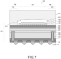
- Fig. 7 is a cross-sectional view showing a configuration example of the solid-state imaging apparatus according to the fifth embodiment.
- the transparent member 321 is provided instead of the transparent member 121 in the above-mentioned first embodiment.
- the other configurations of the solid-state imaging apparatus 300 are the same as the configurations of the solid-state imaging apparatus 100 in the above-mentioned first embodiment.
- a curvature is provided on the bottom surface 324 of the recessed portion surrounded by the projecting portion 122.
- a concave lens can be provided on the bottom surface 324 of the recessed portion surrounded by the projecting portion 122.
- a convex lens may be provided on the bottom surface 324 of the recessed portion surrounded by the projecting portion 122.
- the bottom surface 324 of the recessed portion surrounded by the projecting portion 122 may have a pattern having an optical function.
- the pattern having an optical function may be, for example, a digital lens, or a metalens.
- the other configurations of the transparent member 321 are the same as the configurations of the transparent member 121 in the above-mentioned first embodiment.
- the transparent member 321 is directly joined to the solid-state image sensor chip 101 via the projecting portion 122. At this time, the transparent member 321 is directly joined to the peripheral portion of the imaging region RA via the projecting portion 122 such that a hollow portion 323 is formed on the imaging region RA.
- a curvature is provided on the bottom surface 324 of the recessed portion surrounded by the projecting portion 122. As a result, it is possible to cause the transparent member 321 to have a light collection function and improve the optical performance without increasing the number of parts of the solid-state imaging apparatus 300.
- anti-reflection films 381 and 382 are not formed on the surface of the transparent member 121 in the above-mentioned first embodiment, the anti-reflection films 381 and 382 are formed on the surface of a transparent member 371 in this sixth embodiment.
- Fig. 8 is a cross-sectional view showing a configuration example of a solid-state imaging apparatus according to a sixth embodiment.
- a solid-state imaging apparatus 350 shown in Fig. 8 the transparent member 371 is provided instead of the transparent member 121 in the above-mentioned first embodiment.
- the other configurations of the solid-state imaging apparatus 350 shown in Fig. 8 are the same as the configurations of the solid-state imaging apparatus 100 in the above-mentioned first embodiment.
- the transparent member 371 includes the anti-reflection films 381 and 382 formed on the surface of the transparent member 371 other than the light incident path to the imaging region RA of the solid-state image sensor chip 101.
- the anti-reflection film 381 can be provided on the inner side surface of the projecting portion 122.
- the anti-reflection film 382 can be provided on the outer side surface of the transparent member 371. Further, the anti-reflection film 382 may be provided on the upper surface of the transparent member 371 other than the light incident path to the imaging region RA.
- the materials of the anti-reflection films 381 and 382 may be the same as that of the anti-reflection film 103.
- the anti-reflection films 381 and 382 may have a multilayer structure.
- the anti-reflection film 382 may be extended on the side surface of the solid-state image sensor chip 101.
- the anti-reflection films 381 and 382 are provided in the transparent member 371. As a result, it is possible to suppress stray light and a decrease in sensitivity due to reflection of light that has entered the transparent member 371. For this reason, it is possible to improve the optical performance without increasing the number of parts of the solid-state imaging apparatus 350.
- the anti-reflection film 382 is a light-absorbing film
- the anti-reflection film 382 is disposed in a region other than the light incident path to the imaging region RA of the solid-state image sensor chip 101.
- the antireflection film 382 may be disposed on the imaging region RA of the solid-state image sensor chip 101.
- a moth-eye structure is formed on the side surface of the recessed portion surrounded by a projecting portion 422 of a transparent member 421 in this seventh embodiment.
- Fig. 9 is a cross-sectional view showing a configuration example of a solid-state imaging apparatus according to a seventh embodiment.
- the transparent member 421 is provided instead of the transparent member 121 in the above-mentioned first embodiment.
- the other configurations of the solid-state imaging apparatus 400 shown in Fig. 9 are the same as the configurations of the solid-state imaging apparatus 100 in the above-mentioned first embodiment.
- the projecting portion 422 is provided instead of the projecting portion 122 in the above-mentioned first embodiment.
- the side surface of the recessed portion surrounded by the projecting portion 422 includes a structure 424 that scatters incident light.
- the structure 424 that scatters incident light may be, for example, a moth-eye structure.
- the other configurations of the transparent member 421 are the same as the configurations of the transparent member 121 in the above-mentioned first embodiment.
- the transparent member 421 is directly joined to the solid-state image sensor chip 101 via the projecting portion 422. At this time, the transparent member 421 is directly joined to the peripheral portion of the imaging region RA via the projecting portion 422 such that a hollow portion 423 is formed on the imaging region RA.
- the structure 424 that scatters incident light is provided on the side surface of the recessed portion surrounded by the projecting portion 422. As a result, it is possible to reduce flare due to stray light and improve the optical performance without increasing the number of parts of the solid-state imaging apparatus 400.
- a zigzag shape is formed on the side surface of the recessed portion surrounded by a projecting portion 472 of a transparent member 471 in this eighth embodiment.
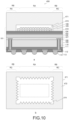
- Fig. 10 is a diagram showing a configuration example of a solid-state imaging apparatus according to an eighth embodiment. Note that Part a of Fig. 10 is a cross-sectional view showing a configuration example of a solid-state imaging apparatus 450, and Part b of Fig. 10 is a plan view showing a configuration example of the transparent member 471.
- the transparent member 471 is provided instead of the transparent member 121 in the above-mentioned first embodiment.
- the other configurations of the solid-state imaging apparatus 450 shown in Fig. 10 are the same as the configurations of the solid-state imaging apparatus 100 in the above-mentioned first embodiment.
- the projecting portion 472 is provided in the transparent member 471 instead of the projecting portion 122 shown in Fig. 1 .
- the side surface of the recessed portion surrounded by the projecting portion 472 includes a structure 474 that scatters incident light.
- the structure 474 that scatters incident light may have, for example, a zigzag shape in plan view. This zigzag shape may have a configuration in which two sides of an isosceles triangle or an equilateral triangle in plan view are arranged along the inner surface of the recessed portion surrounded by the projecting portion 472.
- the other configurations of the transparent member 471 are the same as the configurations of the transparent member 121 in the above-mentioned first embodiment.
- the transparent member 471 is directly joined to the solid-state image sensor chip 101 via the projecting portion 472. At this time, the transparent member 471 is directly joined to the peripheral portion of the imaging region RA via the projecting portion 472 such that a hollow portion 473 is formed on the imaging region RA.
- the structure 474 that scatters incident light is provided on the side surface of the recessed portion surrounded by the projecting portion 472. As a result, it is possible to reduce flare due to stray light and improve the optical performance without increasing the number of parts of the solid-state imaging apparatus 450.
- This solid-state imaging apparatus according to the ninth embodiment is different from the solid-state imaging apparatus according to the first embodiment in that a step that separates the tip of the projecting portion from the end portion of the solid-state image sensor chip is formed in the transparent member.
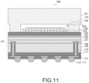
- Fig. 11 is a diagram showing a configuration example of a solid-state imaging apparatus according to a ninth embodiment.
- Fig. 12 is a diagram showing a configuration example of the solid-state imaging apparatus according to the ninth embodiment before being separated into pieces.
- the transparent member 521 is provided instead of the transparent member 121 in the above-mentioned first embodiment.
- the other configurations of the solid-state imaging apparatus 500 shown in Fig. 11 are the same as the configurations of the solid-state imaging apparatus 100 in the above-mentioned first embodiment.
- the projecting portion 522 is provided instead of the projecting portion 122 shown in Fig. 1 .
- the transparent member 521 includes a step 524 that separates the tip of the projecting portion 522 from the end portion of the solid-state image sensor chip 101.
- the step 524 is located on the outer side surface of the projecting portion 522.
- the height of the projecting portion 522 and the position of the step 524 in the height direction of the projecting portion 522 may be equal to or different from each other.
- the shape or the taper angle on the outside and inside of the projecting portion 522 may be equal to or different from each other.
- the other configurations of the transparent member 521 are the same as the configurations of the transparent member 121 in the above-mentioned first embodiment.
- the transparent member 521 is directly joined to the solid-state image sensor chip 101 via the projecting portion 522. At this time, the transparent member 521 is directly joined to the peripheral portion of the imaging region RA while being spaced apart from both end portions of the solid-state image sensor chip 101 via the projecting portion 522.
- the solid-state image sensor chip 101 to which the transparent member 521 is joined is cut from the wafer by being cut at a cutting portion 525 by blade dicing.
- grooves for stopping cracks 554 and 574 are not formed in the solid-state image sensor chip 101 and the transparent member 121, respectively, in the above-mentioned first embodiment, the groove for stopping cracks 554 and 574 are respectively formed in a solid-state image sensor chip 551 and a transparent member 571 in this tenth embodiment.
- This solid-state imaging apparatus is different from the solid-state imaging apparatus according to the first embodiment in that the grooves for stopping cracks are formed in the solid-state image sensor chip and the transparent member.
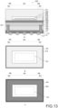
- Fig. 13 is a diagram showing a configuration example of the solid-state imaging apparatus according to the tenth embodiment. Note that Part a of Fig. 13 is a cross-sectional view showing a configuration example of a solid-state imaging apparatus 550, Part b of Fig. 13 is a plan view showing a configuration example of the joint surface of the transparent member 571, and Part c of Fig. 13 is a plan view showing a configuration example of the joint surface of the solid-state image sensor chip 551.
- the solid-state image sensor chip 551 and the transparent member 571 are provided instead of the solid-state image sensor chip 101 and the transparent member 121 in the above-mentioned first embodiment.
- a groove 554 is added to the solid-state image sensor chip 101 in the above-mentioned first embodiment.
- the groove 554 can be provided in the joint region RC of the solid-state image sensor chip 551 along the outer periphery of the solid-state image sensor chip 551.
- the groove 554 may be located in the protective film 104, penetrate the protective film 104 to reach the anti-reflection film 103, or penetrate the protective film 104 and the anti-reflection film 103 to reach the semiconductor substrate 102.
- the groove 554 does not necessarily need to be continuous and may be discontinuous.
- the groove 554 has a width within the range of 2 to 50 ⁇ m and a depth within the range of 10 to 100 ⁇ m and is favorably set within 100 ⁇ m from the end portion of the solid-state image sensor chip 551.
- the other configurations of the solid-state image sensor chip 551 are the same as the configurations of the solid-state image sensor chip 101 in the above-mentioned first embodiment.
- a groove 574 is added to the transparent member 121 in the above-mentioned first embodiment.
- the groove 574 can be provided in the joint region RC of the transparent member 571 along the outer periphery of the transparent member 571.
- the other configurations of the transparent member 571 are the same as the configurations of the transparent member 121 in the above-mentioned first embodiment.
- the grooves 554 and 574 are respectively provided in the solid-state image sensor chip 551 and the transparent member 571. As a result, it is possible to stop, when performing separation into pieces by blade dicing, chipping and cracks that have occurred at the end portion of the solid-state image sensor chip 551 or the end portion of the transparent member 571 at the positions of the grooves 554 and 574 before reaching the imaging region RA, and improve the yield.
- a groove for stopping cracks may be provided in at least one of the solid-state image sensor chip 551 or the transparent member 571.
- a groove for exhausting released gas 602 is not formed in the solid-state image sensor chip 101 in the above-mentioned first embodiment, a linear groove 602 for discharging released gas is formed in a solid-state image sensor chip 601 in this eleventh embodiment.
- Fig. 14 is a diagram showing a configuration example of a solid-state imaging apparatus according to the eleventh embodiment. Note that Part a of Fig. 14 is a cross-sectional view showing a configuration example of a solid-state imaging apparatus 600, Part b of Fig. 14 is a plan view showing a configuration example of the joint surface of the transparent member 121, and Part c of Fig. 14 is a plan view showing a configuration example of the joint surface of the solid-state image sensor chip 601.
- the solid-state image sensor chip 601 is provided instead of the solid-state image sensor chip 101 in the above-mentioned first embodiment.
- the other configurations of the solid-state imaging apparatus 600 shown in Fig. 14 are the same as the configurations of the solid-state imaging apparatus 100 in the above-mentioned first embodiment.
- the groove 602 is added to the solid-state image sensor chip 101 in the above-mentioned first embodiment.
- the groove 602 connects the hollow portion 123 to the outside of the transparent member 121.
- the groove 602 can be located in the protective film 104.
- the groove 602 may include a plurality of grooves or only one groove.
- the other configurations of the solid-state image sensor chip 601 are the same as the configurations of the solid-state image sensor chip 101 in the above-mentioned first embodiment.
- the groove 602 in the solid-state image sensor chip 601 by providing the groove 602 in the solid-state image sensor chip 601, it is possible to cause the gas released from the solid-state image sensor chip 601 to escape to the outside via the groove 602. Therefore, it is possible to prevent damage to the solid-state image sensor chip 601 due to an increase in pressure within the hollow portion 123 and a decrease in optical characteristics due to attachment of the released gas to the transparent member 121.
- the groove 602 favorably has a width of less than 5 ⁇ m and a depth of less than 1 ⁇ m, and more favorably has a width of less than 1 ⁇ m and a depth of less than 10.4 m. As a result, it is possible to prevent moisture from entering the hollow portion 123 in a cleaning step or the like while allowing the released gas to escape via the groove 602, and improve the reliability of the solid-state imaging apparatus 600.
- a groove for exhausting released gas may be provided in at least one of the solid-state image sensor chip 601 or the transparent member 121.
- a groove for exhausting released gas 652 is not formed in the solid-state image sensor chip 101 in the above-mentioned first embodiment, a zigzag groove 652 for discharging the released gas is formed in a solid-state image sensor chip 651 in this twelfth embodiment.
- Fig. 15 is a diagram showing a configuration example of a solid-state imaging apparatus according to the twelfth embodiment. Note that Part a of Fig. 15 is a cross-sectional view showing a configuration example of a solid-state imaging apparatus 650, Part b of Fig. 15 is a plan view showing a configuration example of the joint surface of the transparent member 121, and Part c of Fig. 15 is a plan view showing a configuration example of the joint surface of the solid-state image sensor chip 651.
- the solid-state image sensor chip 651 is provided instead of the solid-state image sensor chip 601 in the above-mentioned eleventh embodiment.
- the other configurations of the solid-state imaging apparatus 650 shown in Fig. 15 are the same as the configurations of the solid-state imaging apparatus 600 in the above-mentioned eleventh embodiment.
- the groove 652 is provided instead of the groove 602 in the above-mentioned eleventh embodiment.
- the groove 652 connects the hollow portion 123 to the outside of the transparent member 121.
- the shape of the groove 652 in plan view is not necessarily limited to a straight line, and may be a zigzag shape or a wavy shape.
- the groove 652 can be located in the protective film 104.
- the groove 652 may include a plurality of grooves or only one groove.
- the other configurations of the solid-state image sensor chip 651 are the same as the configurations of the solid-state image sensor chip 601 in the above-mentioned eleventh embodiment.
- the groove 652 in the solid-state image sensor chip 651 it is possible to allow the gas released from the solid-state image sensor chip 651 to escape to the outside via the groove 652. Therefore, it is possible to prevent damage to the solid-state image sensor chip 651 due to an increase in pressure within the hollow portion 123 and a decrease in optical characteristics due to attachment of the released gas to the transparent member 121. Further, by making the groove 652 have a zigzag shape in plan view, it is possible to suppress moisture from entering the hollow portion 123 in a clearing step or the like while allowing the released gas to escape via the groove 652, and improve the reliability of the solid-state imaging apparatus 650.
- a zigzag groove for exhausting released gas may be provided in at least one of the solid-state image sensor chip 651 or the transparent member 121.
- the groove for stopping cracks554 and the groove for exhausting released gas 602 are not formed in the solid-state image sensor chip 101 in the above-mentioned first embodiment, the groove for stopping cracks554 and the groove for exhausting released gas 602 are formed in a solid-state image sensor chip 701 in this thirteenth embodiment.
- Fig. 16 is a diagram showing a configuration example of a solid-state imaging apparatus according to the thirteenth embodiment. Note that Part a of Fig. 16 is a cross-sectional view showing a configuration example of a solid-state imaging apparatus 700, Part b of Fig. 16 is a plan view showing a configuration example of the joint surface of the transparent member 571, and Part c of Fig. 16 is a plan view showing a configuration example of the joint surface of the solid-state image sensor chip 701.
- the solid-state image sensor chip 701 is provided instead of the solid-state image sensor chip 551 in the above-mentioned tenth embodiment.
- the other configurations of the solid-state imaging apparatus 700 shown in Fig. 16 are the same as the configurations of the solid-state imaging apparatus 550 in the above-mentioned tenth embodiment.
- the groove 602 is added to the solid-state image sensor chip 551 in the above-mentioned tenth embodiment.
- the other configurations of the solid-state image sensor chip 701 are the same as the configurations of the solid-state image sensor chip 551 in the above-mentioned tenth embodiment.
- the grooves 554 and 602 are provided in the solid-state image sensor chip 701, and the groove 574 is provided in the transparent member 571.
- the grooves 554 and 602 are provided in the solid-state image sensor chip 701, and the groove 574 is provided in the transparent member 571.
- a groove for stopping cracks and a groove for exhausting released gas may be provided in at least one of the solid-state image sensor chip 701 or the transparent member 571.
- the above-mentioned embodiments are examples for embodying the present technology, and the matters in the embodiments and the matters specifying the invention in the scope of claims have a corresponding relationship. Similarly, the matters specifying the invention in the scope of claims and the matters having the same names in the embodiments of the present technology have a corresponding relationship.
- the present technology is not limited to the embodiments and can be embodied by making various modifications thereto without departing from the essence of the present technology. Further, the effects described in the present specification are merely examples and are not limited, and other effects may be exhibited.
Landscapes
- Solid State Image Pick-Up Elements (AREA)
Applications Claiming Priority (2)
| Application Number | Priority Date | Filing Date | Title |
|---|---|---|---|
| JP2021191861 | 2021-11-26 | ||
| PCT/JP2022/037345 WO2023095457A1 (ja) | 2021-11-26 | 2022-10-05 | 固体撮像装置および固体撮像装置の製造方法 |
Publications (2)
| Publication Number | Publication Date |
|---|---|
| EP4439670A1 true EP4439670A1 (de) | 2024-10-02 |
| EP4439670A4 EP4439670A4 (de) | 2025-03-05 |
Family
ID=86539236
Family Applications (1)
| Application Number | Title | Priority Date | Filing Date |
|---|---|---|---|
| EP22898242.7A Withdrawn EP4439670A4 (de) | 2021-11-26 | 2022-10-05 | Festkörperbildgebungsvorrichtung und verfahren zur herstellung einer festkörperbildgebungsvorrichtung |
Country Status (4)
| Country | Link |
|---|---|
| US (1) | US20250015110A1 (de) |
| EP (1) | EP4439670A4 (de) |
| CN (1) | CN118160096A (de) |
| WO (1) | WO2023095457A1 (de) |
Family Cites Families (17)
| Publication number | Priority date | Publication date | Assignee | Title |
|---|---|---|---|---|
| US6822326B2 (en) * | 2002-09-25 | 2004-11-23 | Ziptronix | Wafer bonding hermetic encapsulation |
| JP4450168B2 (ja) * | 2002-11-27 | 2010-04-14 | セイコーエプソン株式会社 | 半導体装置の製造方法および半導体装置用カバー |
| JP2004342992A (ja) * | 2003-05-19 | 2004-12-02 | Seiko Epson Corp | 光デバイス及びその製造方法、光モジュール並びに電子機器 |
| JP4672301B2 (ja) * | 2004-07-28 | 2011-04-20 | 富士フイルム株式会社 | 固体撮像装置及び固体撮像装置の製造方法 |
| JP2008166632A (ja) * | 2006-12-29 | 2008-07-17 | Manabu Bonshihara | 固体撮像装置及びその製造方法並びにカメラモジュール |
| JP5226348B2 (ja) | 2008-03-13 | 2013-07-03 | オリンパス株式会社 | 固体撮像装置およびその製造方法 |
| JP2009267049A (ja) | 2008-04-24 | 2009-11-12 | Olympus Corp | 光学装置および光学装置の製造方法 |
| JP5489543B2 (ja) * | 2009-06-09 | 2014-05-14 | キヤノン株式会社 | 固体撮像装置 |
| US8604576B2 (en) * | 2011-07-19 | 2013-12-10 | Opitz, Inc. | Low stress cavity package for back side illuminated image sensor, and method of making same |
| US8946784B2 (en) * | 2013-02-18 | 2015-02-03 | Taiwan Semiconductor Manufacturing Company, Ltd. | Method and apparatus for image sensor packaging |
| JP2015046562A (ja) * | 2013-07-31 | 2015-03-12 | 京セラ株式会社 | 電子素子収納用パッケージおよび電子装置 |
| JP6724777B2 (ja) * | 2014-04-30 | 2020-07-15 | Agc株式会社 | カバーガラス、および、その製造方法 |
| US9978791B2 (en) * | 2015-07-31 | 2018-05-22 | Taiwan Semiconductor Manufacturing Co., Ltd | Image sensor and method for manufacturing the same |
| JP6772450B2 (ja) * | 2015-11-10 | 2020-10-21 | Agc株式会社 | 近赤外線吸収型ガラスウェハおよび半導体ウェハ積層体 |
| CN107958881A (zh) * | 2017-11-28 | 2018-04-24 | 华进半导体封装先导技术研发中心有限公司 | 一种cis器件封装结构及封装方法 |
| KR102578569B1 (ko) * | 2019-01-22 | 2023-09-14 | 주식회사 디비하이텍 | 후면 조사형 이미지 센서 및 그 제조 방법 |
| JP2020136545A (ja) * | 2019-02-21 | 2020-08-31 | ソニーセミコンダクタソリューションズ株式会社 | 固体撮像装置及び電子機器 |
-
2022
- 2022-10-05 US US18/710,294 patent/US20250015110A1/en active Pending
- 2022-10-05 CN CN202280072427.5A patent/CN118160096A/zh active Pending
- 2022-10-05 WO PCT/JP2022/037345 patent/WO2023095457A1/ja not_active Ceased
- 2022-10-05 EP EP22898242.7A patent/EP4439670A4/de not_active Withdrawn
Also Published As
| Publication number | Publication date |
|---|---|
| WO2023095457A1 (ja) | 2023-06-01 |
| US20250015110A1 (en) | 2025-01-09 |
| CN118160096A (zh) | 2024-06-07 |
| EP4439670A4 (de) | 2025-03-05 |
Similar Documents
| Publication | Publication Date | Title |
|---|---|---|
| EP2597860B1 (de) | Bilderfassungsvorrichtung, endoskop und herstellungsverfahren einer bilderfassungsvorrichtung | |
| US7521335B2 (en) | Method and apparatus for producing ultra-thin semiconductor chip and method and apparatus for producing ultra-thin back-illuminated solid-state image pickup device | |
| US8071429B1 (en) | Wafer dicing using scribe line etch | |
| US20080303107A1 (en) | Optical device and method for fabricating the same, camera module using optical device, and electronic equipment mounting camera module | |
| US8500344B2 (en) | Compact camera module and method for fabricating the same | |
| US8778778B2 (en) | Manufacturing method of semiconductor device, semiconductor substrate, and camera module | |
| US20090174018A1 (en) | Construction methods for backside illuminated image sensors | |
| US8338904B2 (en) | Semiconductor device and method for manufacturing the same | |
| US20110304003A1 (en) | Semiconductor device, camera module, and manufacturing method of semiconductor device | |
| US9799588B2 (en) | Chip package and manufacturing method thereof | |
| WO2010086926A1 (ja) | 光学デバイス及びその製造方法 | |
| JP4672301B2 (ja) | 固体撮像装置及び固体撮像装置の製造方法 | |
| JP2010165939A (ja) | 固体撮像装置及びその製造方法 | |
| KR100758887B1 (ko) | 반도체 장치의 제조 방법 | |
| EP4439670A1 (de) | Festkörperbildgebungsvorrichtung und verfahren zur herstellung einer festkörperbildgebungsvorrichtung | |
| US7267603B2 (en) | Back grinding methods for fabricating an image sensor | |
| US20070120041A1 (en) | Sealed Package With Glass Window for Optoelectronic Components, and Assemblies Incorporating the Same | |
| EP4451324A1 (de) | Halbleiterbauelement, elektronische vorrichtung und verfahren zur herstellung eines halbleiterbauelements | |
| US20050158913A1 (en) | Solid state imaging apparatus and its manufacturing method | |
| JP2002006111A (ja) | 撮像装置および実装装置 | |
| US20110042767A1 (en) | Filters in an image sensor | |
| US12272712B2 (en) | Chip package and method for forming a chip package having first and second stack of dummy metal layers surround the sensing region | |
| US20240178261A1 (en) | Chip package and method for forming the same |
Legal Events
| Date | Code | Title | Description |
|---|---|---|---|
| STAA | Information on the status of an ep patent application or granted ep patent |
Free format text: STATUS: THE INTERNATIONAL PUBLICATION HAS BEEN MADE |
|
| PUAI | Public reference made under article 153(3) epc to a published international application that has entered the european phase |
Free format text: ORIGINAL CODE: 0009012 |
|
| STAA | Information on the status of an ep patent application or granted ep patent |
Free format text: STATUS: REQUEST FOR EXAMINATION WAS MADE |
|
| 17P | Request for examination filed |
Effective date: 20240616 |
|
| AK | Designated contracting states |
Kind code of ref document: A1 Designated state(s): AL AT BE BG CH CY CZ DE DK EE ES FI FR GB GR HR HU IE IS IT LI LT LU LV MC ME MK MT NL NO PL PT RO RS SE SI SK SM TR |
|
| REG | Reference to a national code |
Ref country code: DE Ref legal event code: R079 Free format text: PREVIOUS MAIN CLASS: H01L0027146000 Ipc: H10F0039120000 |
|
| A4 | Supplementary search report drawn up and despatched |
Effective date: 20250131 |
|
| DAV | Request for validation of the european patent (deleted) | ||
| DAX | Request for extension of the european patent (deleted) | ||
| RIC1 | Information provided on ipc code assigned before grant |
Ipc: H10F 39/00 20250101ALI20250128BHEP Ipc: H10F 39/12 20250101AFI20250128BHEP |
|
| STAA | Information on the status of an ep patent application or granted ep patent |
Free format text: STATUS: THE APPLICATION HAS BEEN WITHDRAWN |
|
| 18W | Application withdrawn |
Effective date: 20250603 |